

Page 1
.
HALFDUPLEX SYNCHRONOUS FSK MODEM
- TWO PROGRAMMABLE CHANNELS FOR
600BPS DATARATE
- TWO PROGRAMMABLE CHANNELS FOR
1200BPSDATARATE
.
AUTOMATICALL YTUNEDRxANDTxFILTER S
.
TX CARRIER FREQUENCIESSYNTHESIZED
FROMEXTERNALCRYSTAL
.
LOW DISTORTION Tx SIGNAL(S/H2≥ 50dB)
.
AUTOMATICLEVELCONTROLONTxSIGNAL
.
Rx SENSITIVITY: 2mV
3mV
.
Rx CLOCK RECOVERY
.
POWER-DOWN MODE
.
SUITABLETO APPLICATIONIN ACCORDANCE
WITH DH028/29 ENEL, EN50065- 1 CEN ELEC
ANDFCCSPECIFIC AT ION S
RMS
RMS
(600bps)
(1200bps)
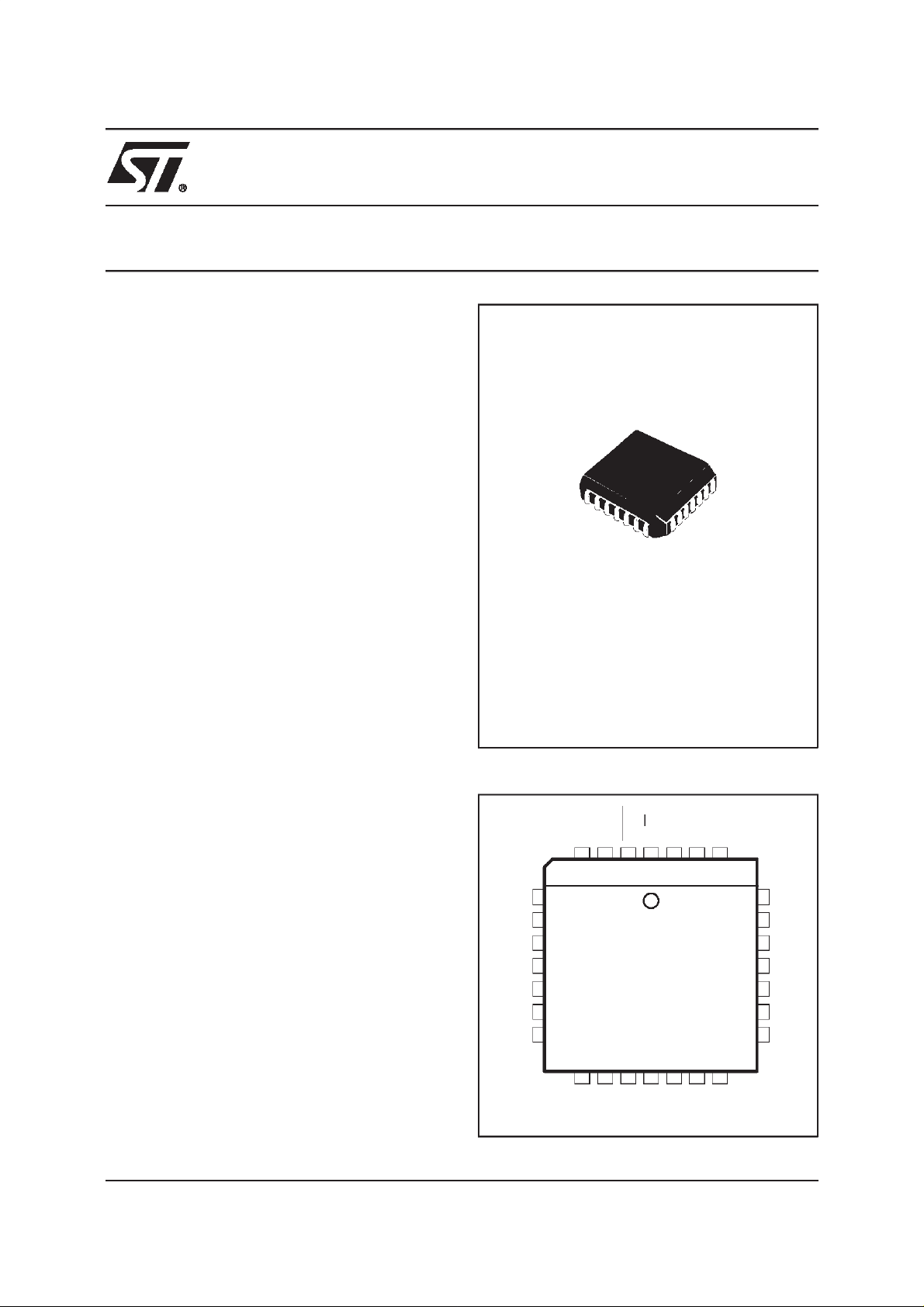
ST7536
POWER LINE MODEM
PLCC28
(Plastic Leaded Chip Carrier Package)
ORDER CODE : ST7536CFN
DESCRIPTION
The ST7536 is a half duplex synchronous FSK
MODEM designed for power line communication
networkapplications.
It operatesfrom a dual powersupply +5V and -5V,
and requires an external interface for the coupling
to the power line. It offerstwo programmable data
ratewith two programmablechannels each.
November 1998
PIN CONNECTIONS
TEST3
4
RxD
CLR/T
RxDEM
DGND
DV
TEST1
TEST2
5
6
7
8
9
DD
10
11
13
12
TxD
TEST4
3
XTAL2
RESET
2
15
14
CHS
XTAL1
Rx/Tx
1
ATO
28
16
BRS
ALCI
27
17
AFCF
TxFI
26
18
SS
DV
25
24
23
22
21
20
19
RxFO
RAI
V
A
DD
AGND
AV
SS
DEMI
IFO
7536-01.EPS
1/9
Page 2

ST7536
PIN DESCRIPTION
Pin
Number
Name Type Description
1 Rx/Tx Digital Rx or Tx modeselection input
2 RESET Digital Logic reset and power-down mode input. Active when low.
3 TEST4 Digital Testinput whichselects the Tx band-pass filter input (TxFI)when high.
4 TEST3 Digital Testinputwhich gives an access to theclockrecovery inputstage. This input isselected
when TEST1 ishigh.
5 RxD Digital Synchronous receive data output
6 CLR/T Digital Rx or Tx clock according to the functional mode
7 RxDEM Digital Demodulated data output
8 DGND Supply Digital ground
9DV
Supply Digitalpositive supply voltage: 5V ± 5%
DD
10 TEST1 Digital Testinput which cancels the Tx to Rx mode automatic switching and validates TEST3
input. Active when high.
11 TEST2 Digital Testinputwhich reduces the Tx to Rxmode automaticswitching time. Active when high.
12 TxD Digital Transmitdata input
13 XTAL2 Digital Crystal oscillator output
14 XTAL1 Digital Crystal oscillator input
15 CHS Digital Channel selection input
16 BRS Digital Baud rate selection input
17 AFCF Analog Automatic frequency control output for connecting compensation network.
18 DV
Supply Digitalnegative supply voltage : -5V ± 5%
SS
19 IFO Analog Intermediate frequency filter output
20 DEMI Analog FSK demodulator input
21 AV
Supply Analog negative supply voltage : -5V±5%
SS
22 AGND Supply Analog ground : 0V
23 AV
Supply Analog positive supply voltage : 5V± 5%
DD
24 RAI Analog Receive analog input
25 RxFO Analog Receive filter output
26 TxFI Analog Transmitfilter input (selected when TEST4 ishigh)
27 ALCI Analog Automatic level control input
28 ATO Analog Analogtransmit output
7536-01.TBL
2/9
Page 3
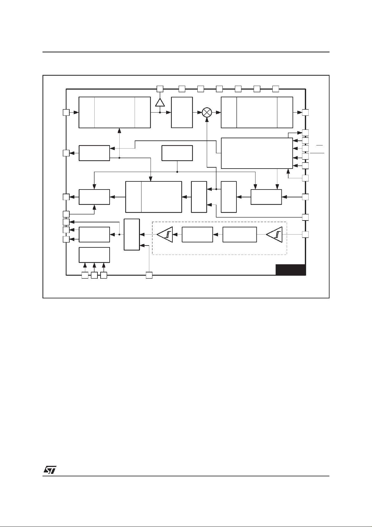
BLOCKDIAGRAM
ST7536
RAI
AFCF
ATO
ALCI
RxDEM
RxD
CLR/T
24
17
28
27
7
5
6
RX BAND-PASS
S.C. FILTER
A.A. FILTER
AFC
ALC
CLOCK
RECOVERY
TEST
LOGIC
SMT. FILTER
TX BAND-PASS
S.C. FILTER
A.A. FILTER
MUX
RxFO DGND AGND
25
DV
SS
18 23
20dB
GAIN
REFERENCE
VOLTAGE
POST-DEMO
S.C. FILTER
MUX
DV
DD
98
CORRELATOR
AV
SS
22
21
I.F. BAND-PASS
S.C. FILTER
A.A. FILTER
TIME BASE AND
CONTROLLOGIC
MODULATOR
A.A. FILTER
FSK DEMODULATOR
FSK
AV
DD
SMT. FILTER
19
13
14
1
2
16
15
12
26
20
IFO
XTAL2
XTAL1
Rx/Tx
RESET
BRS
CHS
TxD
TxFI
DEMI
10
11
TEST1
3
TEST2
TEST4
4
TEST3
ST7536
7536-02.EPS
3/9
Page 4

ST7536
FUNCTIONAL DESCRIPTION
1 - TransmitSection
The transmit mode isset whenRx/Tx = 0, if Rx/Tx
isheldat 0longerthan3s, thenthedeviceswitches
automatically in the Rx mode. A new activation of
the Tx mode requiresRx/Tx to be returnedto 1 for
a minimum2µs period before being set to 0.
The TransmitData (TxD) is sampled on a positive
edgeofCLR/Twhichdeliversthe transmitbitclock
when the transmit mode is selected. This data
entersa FSKmodulatorwhosetwobasicfrequencies are selected by the Baud Rate Selection pin
(BRS) and the Channel Selection pin (CHS) accordingto the Table1.
Figure1 : Tx Data Input Timing
CLR/T
TxD
Table1
BRS CHS
0 0 600 81.75 - 82.35
0 1 600 67.2 - 67.8
1 0 1200 71.4 - 72.6
1 1 1200 85.95 - 87.15
DATA VALID
Baud Rate
(Baud)
Tx Frequencies (kHz)
TxD=1 - TxD=0
These frequ encie s ar e synthesize d fro m a
11.0592MHzcrystaloscillator; theirprecisionisthe
sameas the crystal one’s (100 ppm).
Themodulatedsignalcomingout oftheFSKmodulator is filteredby a switched-capacitorband-pass
filter (Tx band-pass) in order to limit the output
spectrumandto reducethelevelof harmoniccomponents.
The output stage of the Tx path consists of an
AutomaticLevelControl(ALC)systemwhichkeeps
the output signal (ATO) amplitude independantof
thelineimpedancevariations.ThisALCisa variable
gain system(with 32 discretevalues)controlledby
ananalogfeed-back signalALCI (see Figure2).
The ALC gain range is 0dB to -26dB and gain
change is clocked at 7200Hz. Gain steps are of
magnitude0.84dBtypically.
Aperiod of this clock is decomposedinto a 34.7µs
gain settlinglatency and a 104.2µs peakdetecting
time. The gain change is related to the result of a
7536-03.EPS
peak detection obtained by making a direct comparison of ALCI maximum value (during detecting
time)with two thresholdvoltagesV
andVT2(see
T1
Figure2).
- max (VALCI) < V
- The next gain is increased
T1
by 0.84dB,
≤
-V
-V
max(VALCI)≤V
T1
< max (VALCI)- The next gain is decreased
T2
-No gain change,
T2
by 0.84dB.
Figure2 : AutomaticLevel Control Timing Chart
Low Gain Correct Gain
VT2
VT1
ALCI SIGNAL ENVELOP
µs
latency 34.7µs
Gain setting
ALCCLOCK
4/9
Peak detecting
time 104.2
Amplitude
modification
due to an
external cause
High Gain
Correct
Gain
7536-04.EPS
Page 5

FUNCTIONAL DESCRIPTION(continued)
2 - Receive Section
Thereceive section is active when Rx/Tx= 1.
Thebaud rate and channel selectionis also made
accordingto Table1.
The Rx signal is applied on RAI with a common
mode voltage of 0V and filtered by a band-pass
switched capacitor filter (Rx band-pass) centered
onthereceivedcarrierfrequencyandwhosebandwidth is around 6kHz. The input voltage range on
RAI is 2mV
RMS
-2V
RMS
.
TheRxfilteroutputisamplifiedby a20dBgainstage
whichprovidessymmetricallimitationsforlargevoltage. The resulting signal is down-convertedby a
mixer which receivesa local oscillatorsynthesized
bytheFSK modulatorblock.Finallyanintermediate
frequency band-pass filter (IF band-pass) whose
central frequency is 2.7kHz when BRS = 0 and
5.4kHzwhenBRS= 1 improvesthe signalto noise
ratio before entering the FSK demodulator. The
couplingof the intermediatefrequencyfilteroutput
(IFO)tothe FSKdemodulatorinput(DEMI)ismade
byanexternalcapacitorC5(1µF±10%,10V)which
cancelsthe Rx path offset voltage.
A clock recovery circuit extracts the receive clock
(CLR/T) from the demodulated output (RxDEM)
and delivers synchronous data (RxD) on the positiveedge of CLR/T.
ST7536
(47nF±10%,10V)and R1 (1.5kΩ±5%)connected
topin AFCF.
Figure 4 : AutomaticFrequencyLoop Filter
C2
AFCF AGND
17 C1
R1
4 - TestingFeatures
- Anadditionnalamplifierallowsthe observationof
the Rx band-pass filter output on pin RxFO.
- A direct input tothe Tx band-passfilter (TxFI) is
availableand selected when TEST4= 1.
- The 3 second normal duration of the Tx to Rx
mode automatic switching is reducedto 1.48ms
when TEST2 = 1.
- When TEST1 = 1 the Tx to Rx mode automatic
switchingis desactivatedandthe functionalmode
ofthecircuitis controlledbyRx/Txasfollow: when
Rx/Tx = 0 the circuit is transmittingcontinuously,
whenRx/Tx=1theclockrecoveryblockisdisconnectedfromtheFSK demodulatorfor testingpurpose,inthisconfigurationTEST3isthe datainput
oftheclockrecoveryblock,RxDEMfollowTEST3
andRxD deliversthe resynchronizeddata.
22
7536-06.EPS
Figure3 : RxData Output Timing
CLR/T
RxD DATA VALID
3 -Additional Digital and Analog Functions
Areset intput (RESET) initializesthe device.
When RESET = 0, the device is in power-down
mode and all the internal logic is reset. When
RESET= 1, the device is active.
Atime base section delivers all the internalclocks
froma crystal oscillator (11.0592MHz).Thecrystal
isconnectedbetweenXTAL1andXTAL2pins and
needstwoexternalcapacitorsC3 and C4 depending on t he cryst al ch aracte ristic typically
22pF ±10% for properoperation.Itisalsopossible
to providedirectly the clock on pin XTAL1 ; in this
caseC3 and C4 should be removed.
An Automatic Frequency Control (AFC) Section
adjusts the central frequency of Rx and Tx bandpass filter to the carrier central frequency. The
stabilityof the AFC loop is ensured by an external
compensationnetworkC1 (470nF ±10%,10V), C2
5 - Power Supplies Wiring and Decoupling
Precautions
The ST7536 has two positive power supply pins,
two negative power supply pins and two ground
pinsinordertoseparate internalanaloganddigital
supplies.The analog and digital terminals of each
7536-05.EPS
supplypair must be connectedtogetherexternally
and require special routingprecautionsin order to
get the best receivesensitivity performances.
The three major routingrequirementsare :
- The ground impedance should be as low as
possible, for this purpose the AGND an DGND
terminalscan be connectedvia a localplane.
- Thepositiveandnegativepowersupplies(AV
,AVSS,DVSS) should be star-connected,
DV
DD
avoidingcommon current path for the digitaland
analog power supplies terminals.
- Five decoupling capacitors located as close as
possibleto the powersupplyterminalsshouldbe
used. Two 2.2µF tantalum and two 100nF ceramic capacitors perform the main decoupling
function in the vicinity of the analog power suppliesanda100nFceramiccapacitorinthevicinity
of the positive digital power supply is used to
reduce the high frequency perturbations generated by the logicpart of the circuit.
DD
5/9
,
Page 6

ST7536
ABSOLUTE MAXIMUMRATINGS
Symbol Parameter Value Unit
/DV
AV
DD
/DV
AV
SS
V
AGND/DGND
V
I
V
O
I
O
V
i
V
o
I
o
P
D
T
oper
T
stg
Notes : 1. The voltages are referenced to AGND andDGND.
2. Latch-up problems can be overcome with 2 reverse biased schottky diodes connected respectively between A/DV
andA/DV
3. Absolutemaximum ratings are values beyondwhich damage todevice may occur. Functionaloperation under theseconditions is
not implied.
GENERAL ELECTRICALCHARACTERISTICS
Thetest conditionsare A/DV
T
= -10 to 70oC unlessotherwisespecified
amb
Symbol Parameter Test Conditions Min. Typ. Max. Unit
AV
/DV
DD
AV
/DV
SS
AI
+DIDDPositive Supply Current in Tx Mode RESET = 1, RX/Tx = 0 30 35 mA
DD
AIDD+DIDDPositive Supply Current in Rx Mode RESET = 1, RX/Tx = 1 29 34 mA
AI
+DISSNegative Supply Current in Tx Mode RESET = 1, RX/Tx = 0 - 34 - 29 mA
SS
AISS+DISSNegative Supply Current in Rx Mode RESET = 1, RX/Tx = 1 - 33 - 28 mA
AI
+DIDDPositive Power-down Current
DD
AI
+DISSNegative Power-down Current - 1.2 mA
SS
V
IH
V
IL
V
OH
V
OL
V
IH
DC XTAL1Clock Duty Cycle Externalclock 40 60 %
Positive Supply Voltage(1) -0.3, +7 V
DD
Negative Supply Voltage(1) -7, +0.3 V
SS
Voltagebetween AGND and DGND -0.3, +0.3 V
Digital Input Voltage DGND-0.3, DVDD+0.3 V
Digital Output Voltage DGND-0.3, DVDD+0.3 V
Digital Output Current -5, +5 mA
Analog Input Voltage AVSS-0.3, AVDD+0.3 V
Analog Output Voltage AVSS-0.3, AVDD+0.3 V
Analog Output Current -5, +5 mA
Power Dissipation 500 mW
Operating Temperature - 25, + 70
Storage Temperature - 65, + 150
&A/DGND.
SS
= +5V,A/DVSS= -5V,A/DGND= 0V,
DD
Positive Supply Voltage 4.75 5 5.25 V
DD
Negative Supply Voltage -5.25 -5 -4.75 V
SS
RESET = 0, RX/Tx = 1
XTAL1= 1
High LevelInput Voltage Digital inputs except XTAL1 2.2 V
Low Level Input Voltage Digitalinputs 0.8 V
High LevelOutput Voltage Digitaloutputs, IOH= - 400µA 2.4 V
Low Level Output Voltage Digital outputs, IOL= 1.6mA 0.4 V
High LevelInput Voltage XTAL1input 3.6 V
&A/DGND
DD
1.2 mA
o
C
o
C
7536-02.TBL
7536-03.TBL
6/9
Page 7

ST7536
TRANSMITTER ELECTRICALCHARACTERISTICS
Thetest conditionsare A/DV
T
= -10 to +70oC unless othewisespecified
amb
Symbol Parameter Test Conditions Min. Typ. Max. Unit
V
Max Carrier Output AC Voltage RL=2kΩ,V
TAC
HD2 Second Harmonic Distortion RL=2kΩ,V
FD FSKPeak-to-peak Deviation BRS = 0
TRxTx Carrier Activation Time After Rx/Tx 1 → 0 transition 1 ms
TALC Carrier Stabilisation Time ALC maximum settling time, 32 gain steps 5 ms
DRNG ALC Dynamic Range 25 26 27 dB
VT1 ALC Low Threshold Voltage 1.81 1.87 V
VT2 ALC High Threshold Voltage 2.12 2.18 V
GST ALC Gain Step 0.84 dB
PSRR1
PSRR2
Note 1 : This characteristic is guaranteed by correlation.
Power supply rejection ratio on ATO
(see Note 1)
RECEIVERELECTRICAL CHARACTERISTICS
Thetest conditionsare A/DV
= -10 to +70oC unless othewisespecified
T
amb
Symbol Parameter Test Conditions Min. Typ. Max. Unit
Maximum Input Signal 2V
V
IN
R
Input Impedance 100 kΩ
IN
RCJ Recovered Clock Jitter Percentage of the nominal clock - 5 + 5 %
PSRR1
PSRR2
V
V
BER1
BER2
BER3 Bit error rate at maximum Rx sig-
BER4 Biterrorrateat medium Rx signal
BER5 Bit error rate with impulsive noise
BER6
BER7
Note 1 : This characteristic is guaranteed by correlation
Power supply rejection ratio on
RxFO (see Note 1)
Rx sensitivity (see Note 1) Typical measured BER < 10
IN0
IN1
Bit error rate at minimum Rx
signal (seeNote 1)
nal (see Note 1)
(see Note 1)
(see Note 1)
Bit error rate with modulated
sinusoidal noise Ns (see Note 1)
= +5V,A/DGND= 0V,A/DVSS=-5V,
DD
ALCI<VT1
ALCI<VT1
BRS = 1
V
= 200mVPP,fIN= 50Hz on VDDor V
IN
= +5V,A/DGND= 0V,A/DVSS=-5V,
DD
= 200mVPP,fIN= 50Hz on VDDor V
V
IN
BRS = 0
BRS = 1
White Noise, S/N = 15dB
RAI = 2mV
RAI = 3mV
RAI = 2V
RAI= 0.6V
RMS
RMS
RAI = 90mV
f = 100Hz, duty cycle = 10%
S+ Ns < 0.2V
80% AM modul.,f
= 2mV
S
min
= 3mV
S
min
, BRS = 0
RMS
, BRS = 1
RMS
, White Noise, S/N =25dB 10
, S/N= 15dB 10
,N=5VPPpulsewave,
RMS
, Ns = sine carrier with
RMS
= 1kHz, See Figure 5
m
, BRS = 0
RMS
, BRS = 1
RMS
2.8 3.2 3.7 V
0.32 %
600
1200
35
SS
10
35
SS
-5
10
dB
dB
mV
2
3
-5
2 ⋅ 10
3 ⋅ 10
-3
10
-4
-3
10
-7
-3
10
-6
-3
10
-3
10
-3
10
-3
10
PP
Hz
Hz
dB
dB
RMS
RMS
7536-04.TBL
7536-05.TBL
7/9
Page 8

ST7536
Figure5 : S/N Maskfor 80%AM Sine Noise
S/N (dB)
20
10
-10
-20
-30
-40
-50
S
0
0 0.5 1 1.5 2
B
Frequency (f/fc)
B = 20kHz at 600 Bit/s (BRS = 0)
B = 40kHz at 1200 Bit/s -BRS = 1)
FILTER TEMPLATES
Frequency
(kHz)
Test
Conditions
RECEIVE AND TRANSMIT FILTER
54
79.05 - 4 - 3 - 2
Ref 82.05 0
BRS = 0,
CHS = 0
85.05 - 4 - 3 - 2
123 - 35
44.4
65 -4 -3 -2
Ref 67.46 0
BRS = 0,
CHS = 1
69.93 - 4 - 3 - 2
101.13 - 35
47.57
69.64 - 4 - 3 - 2
Ref 72.28 0
BRS = 1,
CHS = 0
74.92 - 4 - 3 - 2
108.36 - 35
57.08
83.57 - 4 - 3 - 2
Ref 86.74 0
BRS = 1,
CHS = 1
89.91 - 4 - 3 - 2
130.03 - 35
Amplitude (dB)
Min. Typ. Max.
-35
-35
-35
-35
fc : Central Carrier Frequency
Frequency
(kHz)
Test
Conditions
Amplitude (dB)
Min. Typ. Max.
INTERMEDIATE FREQUENCY FILTER
1.2
2.15 - 5 - 3 - 2
Ref 2.7 0
BRS = 0
3.25 - 5 - 3 - 2
5.8 - 35
2.4
4.3 -5 -3 -2
Ref 5.4 0
BRS = 1
6.5 -5 -3 -2
11.6 - 35
7536-07.EPS
-35
-35
7536-06.TBL
8/9
Page 9

PACKAGE MECHANICALDATA
28 PINS - PLASTIC LEADED CHIP CARRIER (PLCC)
ST7536
Dimensions
Min. Typ. Max. Min. Typ. Max.
Millimeters Inches
A 12.32 12.57 0.485 0.495
B 11.43 11.58 0.450 0.456
D 4.2 4.57 0.165 0.180
D1 2.29 3.04 0.090 0.120
D2 0.51 0.020
E 9.91 10.92 0.390 0.430
e 1.27 0.050
e3 7.62 0.300
F 0.46 0.018
F1 0.71 0.028
G 0.101 0.004
M 1.24 0.049
M1 1.143 0.045
Information furnished is believed to be accurate and reliable. However, STMicroelectronics assumes no responsibility for the
consequences of use of such information nor for any infringement of patents or other rights of third parties which may result from
its use. No licence is granted by implication or otherwise under any patent or patent rights of STMicroelectronics. Specifications
mentioned in this publication are subject to change without notice. This publication supersedes and replaces all information
previouslysupplied.STMicroelectronicsproductsare notauthorizedforuse as criticalcomponentsinlifesupport devicesor systems
without express written approval of STMicroelectronics.
Purchase of I
Rights to use these components in a I
Australia - Brazil - Canada- China - France - Germany - Italy - Japan - Korea - Malaysia - Malta- Mexico - Morocco - The Netherlands
Singapore - Spain - Sweden - Switzerland - Taiwan- Thailand - United Kingdom - U.S.A.
The ST logo is a registered trademark of STMicroelectronics
1998 STMicroelectronics- All Rights Reserved
2
C Components of STMicroelectronics, conveys a licenseunder the Philips I2C Patent.
2
C Standard Specifications as defined by Philips.
the I
STMicroelectronics GROUP OF COMPANIES
2
C system, is granted provided that the system conforms to
http://www.st.com
9/9
PMPLCC28.EPS
PLCC28.TBL
 Loading...