

Datasheet ST735TCN, ST735TCD-TR, ST735TCD, ST735SCD-TR, ST735SCN Datasheet (SGS Thomson Microelectronics)
...Page 1
300kHz, -5V/ADJ INVERTING, NEGATIVE OUTPUT
CURRENT-MODE PWM REGULATOR
■ CONVERTS +4.0V TO + 6.2V INPUT TO -5V
OUTPUT (735S) OR +3.5V TO + 9.0V TO A
NEGATIVE ADJUSTABLE OUTPUT (735T)
■ 1W GUARANTEEDOUTPUT POWER
■ 72% TYPICAL EFFICIENCY
■ 0.8mA QUIESCENT CURRENT
■ 1µA SHUTDOWN MODE
■ 300KHZ FIXED FREQUENCY OSCILLATOR
■ CURRENT MODE PWM CONVERTER
■ LOW NOISE AND JITTER
■ SOFT START
■ SIMPLE APPLICATION CIRCUIT
■ UNDERVOLTAGE LOCKOUT (735S)
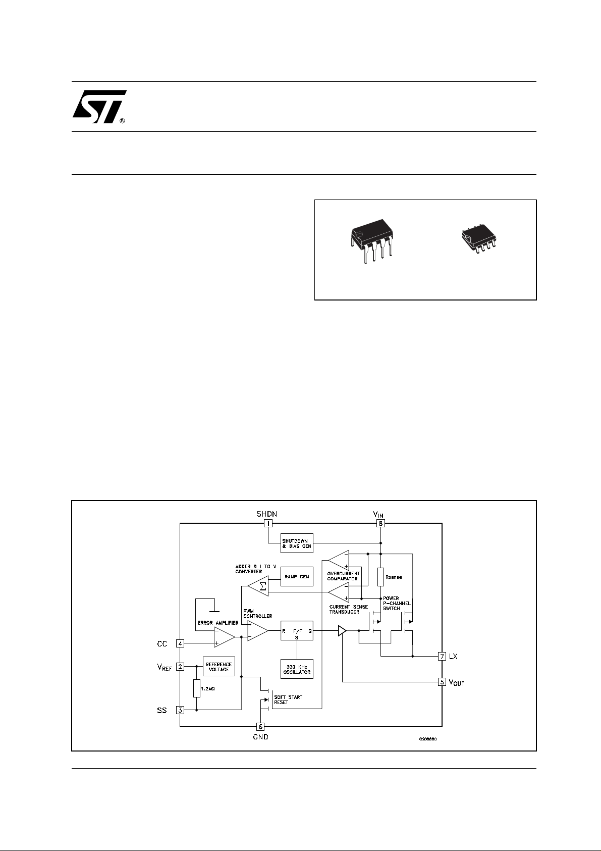
DESCRIPTION
The ST735S/ST735T is a Bi-CMOS, inverting
switch mode DC-DC regulator wi th internal Power
MOSFET that generates a fixed -5V (S version) or
a negative adjustable (T version) output voltage
from a 4V (3.5V for the 735T) to 6.2V input voltage
(9V for the 735T); is gu arante ed an output current
of 200mA for inputs greater than 4.5V. The
quiescent current for this device is typically of
ST735S
ST735T
DIP-8 SO-8
0.8mA and, in shutdown mode it is reduced to
1µA.
These power-conserving features, along with high
efficiency and appli cations circuits, thaT lend itself
to minaturization, make the ST735S/ST735T
excellent in a broad range of on-card, HDD and
portable equipment applications. These device
employ a high performance c urrent mode pu lse
with modulation (PWM) control scheme to provide
tight output voltage regulation and low noise. The
fixed frequency oscillator is factory trimmed to
300KHz, a llowing for easy noise filtering. The
regulator in production is tested to guarantee an
output accuracy within ±5% over all specified
conditions.
SCHEMATIC DIAGRAM
1/11October 2002
Page 2
ST735S/ST735T
ABSOLUTE MAXIMUM RATINGS
Symbol Parameter Value Unit
V
V
SHDN
V
V
V
OUT
I
LX
P
T
T
Absolute Maximum Ratings are those values beyond which damage to the device may occur. Functional operation under these condition is
not implied.
Note 1: The input to output differential voltage is limited to VIN+|V
THERMAL DATA
DC Input Voltage (VINto GND) for ST735S
IN
DC Input Voltage (VINto GND) for ST735T (Note 1)
IN
Shutdown Voltage (SHDN to GND) -0.3 to V
Switch Voltage (Lx to VIN)
LX
Feedback Voltage (V
FB
Output Voltage (V
OUT
to GND)
OUT
to GND)
Other Input Voltage (SS, CC to GND) -0.3 to V
Peack Switch Current
Power Dissipation at Tj= 70°C DIP-8 725
tot
Storage Temperature Range
stg
Operating Junction Temperature Range
op
OUT
|<12.7V
SO-8 470
-0.3 to +7 V
-0.3 to +11 V
IN
+0.3
V
-12.5 to +0.3 V
-11to+0.3 V
-11to+0.3 V
+0.3
+
V
2A
mW
-55 to +150 °C
-40 to +125 °C
Symbol Parameter DIP-8 SO-8 Unit
R
thj-case
Thermal Resistance Junction-case
2 8 °C/W
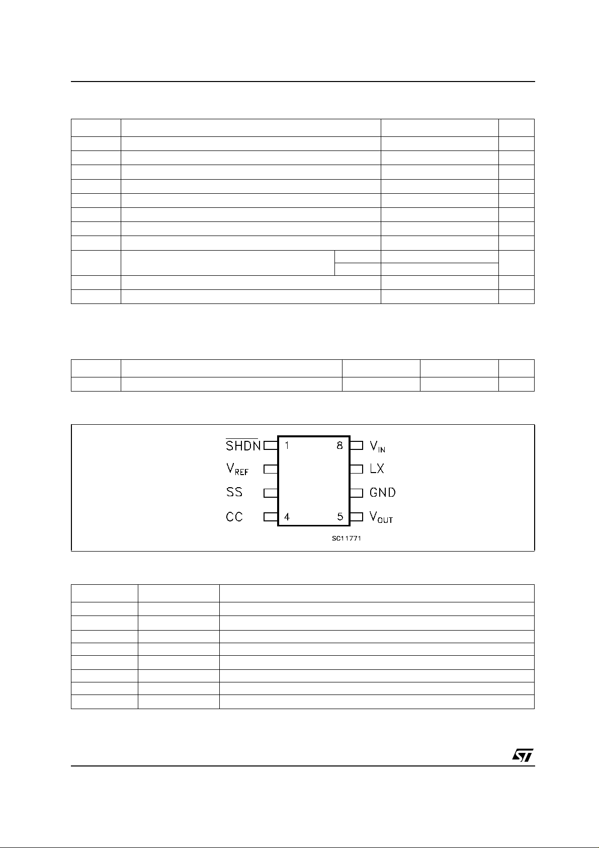
CONNECTION DIAGRAM (top v iew)
PIN DESCRIPTION
Pin N° Symbol Name and Function
1 SHDN SHUT-DOWN Control (V
2V
REF
Reference Output Voltage
3 SS Soft Start
4 CC Compensation Input
5V
OUT
Negative Output Voltage
6 GND Ground
7 LX Switch Output
8V
IN
Positive Supply - Voltage Input
=ON GND=Shutdown
CC
2/11
Page 3
ORDERING CODES
TYPE DIP-8 SO-8 SO-8 (T&R)
ST735S ST735SCN ST735SCD ST735SCD-TR
ST735T ST735TCN ST735TCD ST735TCD-TR
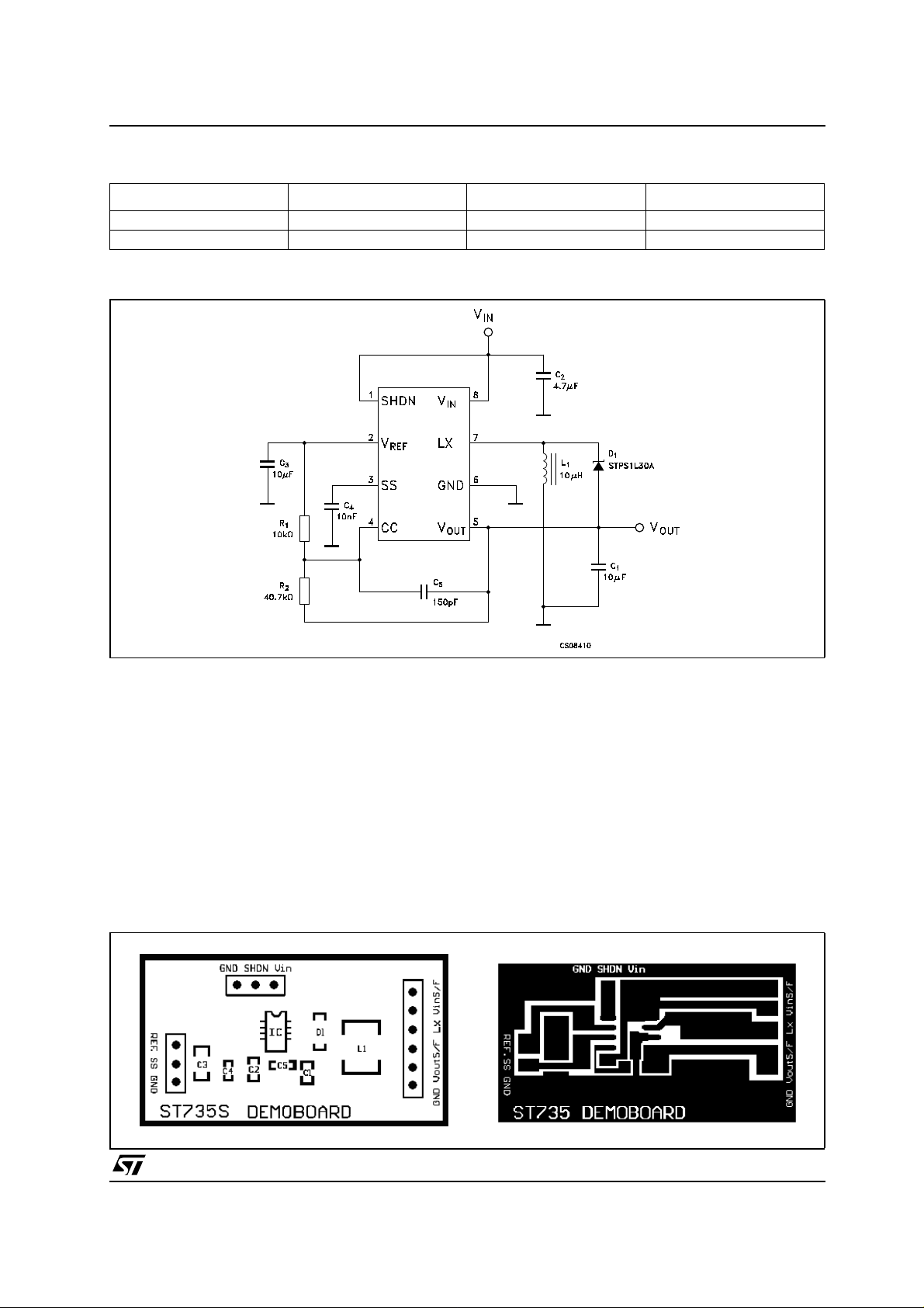
TYPICAL APPLICATION CIRCUIT
ST735S/ST735T
NOTE:
1) All capacitors are X7R ceramic
can be omitted if are used higher values for the input and output capacitors (suggested C2=47µF, C1=100µF).
2) C
5
3) R
and R2must be placed is ST735T applications only. Their values are calculated by the following formula R2=(|V
1
can be chosen any value between 2kΩ and 20kΩ
APPLICATION CIRCUIT
To achieve the best performances from switching
power supply topology, p articular care to layout
drawing is needed, in order to minimize EMI and
obtain low noise. Moreover, jitter free op eration
ensures the full device fun ctionality. Layout desi gn
proposed on demoboard helps to lower the
developing time. Wire lengths must be minimized,
filter and bypass capacitors m ust be low ESR
type, placed as close as possible to the integrated
circuit. T he 4.7µF (or 6.8µF) inductor must be
chosen built on a core, taking care that saturation
current should be h igher than the peak LX switch
current. See the Peak Inductor Current vs Output
Current graph.
PRINTED DEMOBOARD (not in scale)
OUT
|/V
REF
)xR1.ForR
1
3/11
Page 4
ST735S/ST735T
ELECTRICAL CHARACTERISTICS OF ST735S (Refer to test circuit,VIN=5V,CIN=4.7µF, C
all X7R ceramic, L = 4.7µH(Note1),I
value are referred at T
amb
= 25°C)
OUT
=0mA,T
= -40 to 125°C, unless otherwise specified. Typical
amb
OUT
=10µF
Symbol Parameter Test Conditions Min. Typ. Max. Unit
V
V
I
I
SUPPLY
I
STANDBY
I
PEAK
V
∆V
∆V
V
∆V
R
DSON
I
LEAK
V
f
R
Note 1: Utilize of 6.8µH permits to reach higher current capability at the same operating conditions
Note2: Guaranteed by design, but not tested in production
Note3 : Tested at I
Input Voltage 4 6.2 V
IN
Output Voltage VIN= 4.5V to 6.2V I
OUT
T
amb
V
IN
T
amb
OUT
Output Current
V
V
T
V
IN
IN
amb
IN
= -40 to 125°C
= 4.0V to 6.2V I
= -40 to 125°C
= 4.5V to 6.2V TJ= 0 to 125°C
= 4.5V to 6.2V I
= -40 to 125°C
= 4.0V V
OUT
= 0 to 200mA
OUT
= 0 to 175mA
OUT
-5.25 -5 -4.75 V
-5.25 -5 -4.75 V
200 275 mA
= 0 to 175mA
OUT
175 mA
= -5V 175 mA
Supply Current Includes Switch Current 0.8 1.6 mA
Standby Current V
Short Circuit Current VIN= 5V 0.9 A
I
SC
=0V 1 10 µA
SHDN
LX Max Peak Current (Note 2) 1.5 A
Undervoltage Lock-out 3.5 4 V
LO
Line Regulation VIN= 4.0V to 6.2V 0.1 %/V
OUT
Load Regulation I
OUT
Reference Voltage
REF
Reference Drift
REF
= 0 to 200mA 0.003 %/mA
OUT
T
=25°C (Note 3)
amb
T
= -40 to 125°C
amb
1.225 V
50 ppm/°C
LX ON Voltage 0.5 Ω
LX Leakage Current VDS= 10V 1 µA
Shutdown Pin Current 1 µA
I
SH
V
Shutdown Input Low
IL
Threshold
Shutdown Input High
IH
Threshold
Maximum Oscillator
OSC
Frequency
ν Efficency I
Compensation Pin
CC
Impedance on CC Pin
= 125µA
VREF
= 100mA 72 %
OUT
2V
300 KHz
7.5 KΩ
0.25 V
4/11
Page 5

ST735S/ST735T
ELECTRICAL CHARACTERI STIC S OF ST735T (Refer to t es t circuit, VIN=5V, CIN=4.7µF, C
allX7Rceramic,L=4.7µH(Note1) , I
=0mA,VOadjustedto-5V,T
OUT
= -40to125°C,unlessotherwise
amb
OUT
=10µF
specified. Typical value are referred at Tamb= 25°C)
Symbol Parameter Test Conditions Min. Typ. Max. Unit
V
I
SUPPLY
I
STANDBY
I
PEAK
V
∆V
∆V
V
∆V
R
DSON
I
LEAK
V
f
R
Note 1: Utilize of 6.8µH permits to reach higher current capability at the same operating conditions
Note2: Guaranteed by design, but not tested in production
Note3 : Tested at I
Input Voltage 3.5 9 V
IN
Output Voltage VIN= 4.5V to 6.2V I
V
O
T
amb
V
IN
T
amb
I
O
Output Current
V
V
T
V
IN
IN
amb
IN
= -40 to 125°C
= 4.0V to 6.2V I
= -40 to 125°C
= 4.5V to 6.2V T
= 4.5V to 6.2V I
= -40 to 125°C
= 4.0V V
OUT
= 0 to 200mA
OUT
= 0 to 175mA
OUT
= 0 to 125°C
amb
= 0 to 175mA
OUT
-5.25 -5 -4.75 V
-5.25 -5 -4.75 V
200 275 mA
175 mA
= -5V 175 mA
Supply Current Includes Switch Current 0.8 1.6 mA
Standby Current V
Short Circuit Current VIN= 5V 0.9 A
I
SC
=0V 1 10 µA
SHDN
LX Max Peak Current (Note 2) 1.5 A
Undervoltage Lock-out 3.5 4 V
LO
Line Regulation VIN= 4.0V to 6.2V 0.1 %/V
OUT
Load Regulation I
OUT
Reference Voltage
REF
Reference Drift
REF
= 0 to 200mA 0.003 %/mA
OUT
T
=25°C (Note 3)
amb
T
= -40 to 125°C
amb
1.225 V
50 ppm/°C
LX ON Voltage 0.5 Ω
LX Leakage Current VDS= 10V 1 µA
Shutdown Pin Current 1 µA
I
SH
V
Shutdown Input Low
IL
Threshold
Shutdown Input High
IH
Threshold
Maximum Oscillator
OSC
Frequency
ν Efficency I
Compensation Pin
CC
Impedance on CC Pin
= 125µA
VREF
= 100mA 72 %
OUT
2V
300 KHz
7.5 KΩ
0.25 V
5/11
Page 6

ST735S/ST735T
TYPICAL CHARACTERISTICS
(Referredto typical application circuit,T
Figure1 : Output Voltage vs Temperature
Figure2 : Reference Voltage vs Temperature
=25°C unless otherwise specified)
amb
Figure4 : Efficency vs Ouput Current
Figure5 : Efficency vs Low Ouput Current
Figure3 : EfficencyvsTemperature
6/11
Figure6 : Supply Currentvs Temperature
Page 7

ST735S/ST735T
Figure7 : Supply Current vs Input Voltage for
ST735S
Figure8 : Supply Current vs Input Voltage for
ST734T
Figure10 : Peack Inductor vs Output Current
Figure11 : Switch Current Li mi t vs Soft Start
Voltage
Figure9 : Shutdown Threshold vs Temperature
Figure12:Oscillator Frequency Vs Temperature
7/11
Page 8

ST735S/ST735T
V
I
200mA,C
C
100µF
V
I
200mA,C
C
100µF
V
I
200mA,C
C
100µF
V
I
100mA
Figure13 : LX On Resist ance vs Temperature
Figure14 : LX On Res istance vs Input Voltage
Figure16 : Load Transient
=5V,
=20mAto
I
O
=4.7µF,
I
Figure17 : Load Transient
=
O
,tf=1µs
Figure15 : Load Transient
=5V,
I
8/11
=20mAto
O
=4.7µF,
I
=5V,
=20mAto
I
O
=4.7µF,
I
=
O
,tr=1µs
Figure18 : Switching Waveform
=
O
,tr=tf=1µs
=5V,
I
=
O
Page 9

Plastic DIP-8 MECHANICAL DATA
ST735S/ST735T
DIM.
MIN. TYP MAX. MIN. TYP. MAX.
A 3.3 0.130
a1 0.7 0.028
B 1.39 1.65 0.055 0.065
B1 0.91 1.04 0.036 0.041
b 0.5 0.020
b1 0.38 0.5 0.015 0.020
D 9.8 0.386
E 8.8 0.346
e 2.54 0.100
e3 7.62 0.300
e4 7.62 0.300
F 7.1 0.280
I 4.8 0.189
L 3.3 0.130
Z 0.44 1.6 0.017 0.063
mm. inch
P001F
9/11
Page 10

ST735S/ST735T
SO-8 MECHANICAL DATA
DIM.
A 1.75 0.068
a1 0.1 0.25 0.003 0.009
a2 1.65 0.064
a3 0.65 0.85 0.025 0.033
b 0.35 0.48 0.013 0.018
b1 0.19 0.25 0.007 0.010
C 0.25 0.5 0.010 0.019
c1 45˚ (typ.)
D 4.8 5.0 0.189 0.196
E 5.8 6.2 0. 228 0.244
e 1.27 0.050
e3 3.81 0.150
F 3.8 4.0 0.149 0.157
L 0.4 1.27 0.015 0.050
M 0.6 0. 023
S
MIN. TYP MAX. MIN. TYP. MAX.
mm. inch
˚ (max.)
8
10/11
0016023
Page 11

ST735S/ST735T
Information furnished is believed to be accurate and reliable. However, STMicroelectronics assumes no responsibilit y for the
consequences of use of such informatio n nor for any infringement of paten ts or o ther rig hts of t hird part ies which ma y result from
its use. No license is granted by implication or otherwise under any patent or patent rights of STMicroelectronics. Specifications
mentioned in this publication are subject to change without notice. This publication supersedes and replaces all information
previousl y suppl ied. STM icroel ectronics produc ts are not auth orized for use as c ritica l compone nts in l ife s upport dev ices or
systems without express written approval of STMicroelectronics.
Australia - Brazil - Canada - China - Finland - France - Germany - Hong Kong - India - Israel - Italy - Japan - Malaysia - Malta - Morocco
© The ST logo is a registered trademark of STMicroelectronics
© 2002 STMicroelectronics - Printed in Italy - All Rights Reserved
STMicroelectronics GROUP OF COMPANIES
Singapore - Spain - Sweden - Switzerland - United Kingdom - United States.
© http://www.st.com
11/11
 Loading...