

Datasheet ST730ACD-TR, ST730ABN, ST730ACD, ST730ABD-TR, ST730ABD Datasheet (SGS Thomson Microelectronics)
Page 1
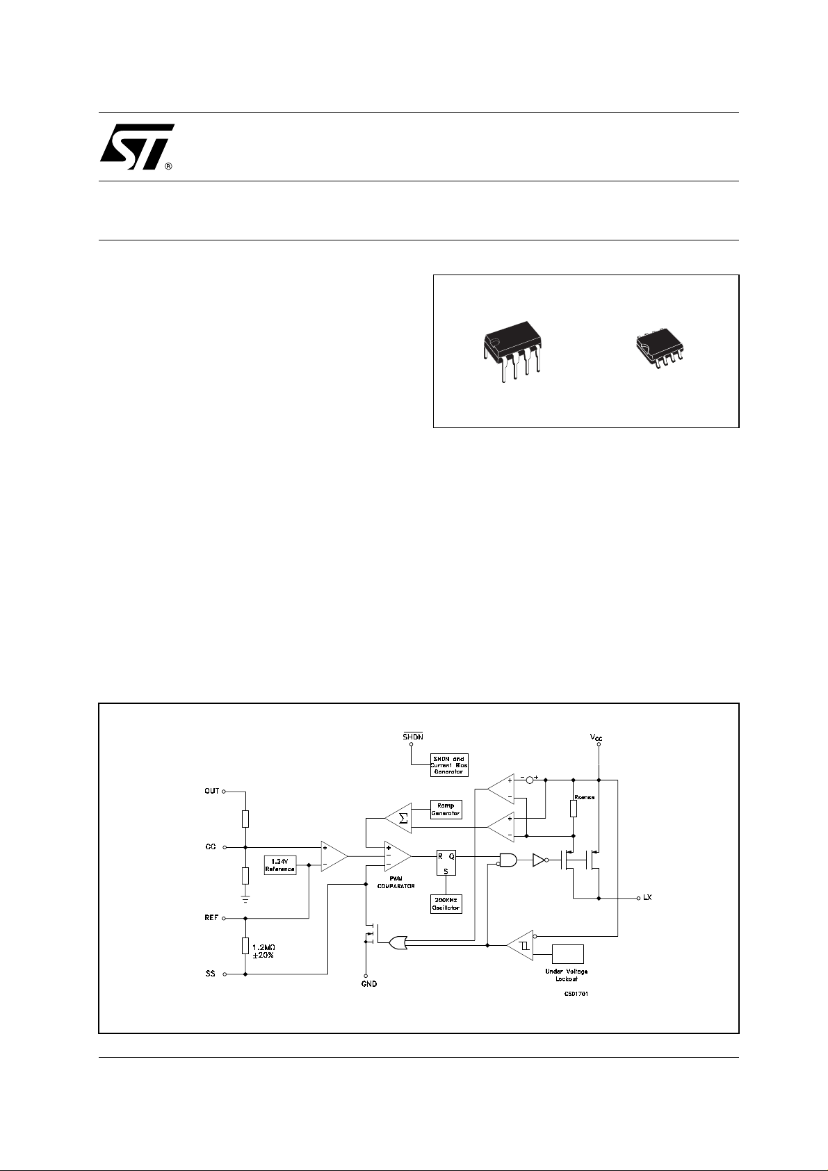
CURRENT-MODE PWM DC-DC CONVERTERS
■ UP TO 450mA LOAD CURRENTS
■ 200kHz HIGH-FREQUENCY
CURRENT-MODE PWM
■ 85% TO 96% EFFICIENCIES
■ 33µHOR100µH PRE-SELECTED
INDUCTOR VALUE, NO COMPONENT
DESIGN REQUIRED
■ 0.8mA QUIESCENT CURRENT
■ 0.3µA SHUTDOWN SUPPLY CURRENT
■ ADJUSTABLE OUTPUT VOLTAGE
■ OVERCURRENT, SOFT-START AND
UNDERVOLTAGE LOCKOUT PROTECTION
■ CYCLE-BY-CYCLE CURRENT LIMITING
■ PACKAGE AVAILABLE: DIP-8 AND SO-8
DESCRIPTION
The ST730A is a 5V output CMOS, step-down
switching regulator. The ST730A accepts inputs
between 5.2V and 11V and delivers 450mA.
Typical efficiencies are 85% to 96%.
Quiescent supply current is0.8mA and o nly 0.3µA
in shutdown mode. The output does not exhibit
frequency over this specified range. Pulse-width
modulation (PWM) current-mode control provides
ST730A
5V STEP-DOWN,
DIP-8 SO-8
precise o utput regulation and excellent transient
responses. Output voltage accuracy is
guaranteed to be ±5% over line, load, and
temperature varations.
Fixed-frequency switching and absence of
subharmonic ruipple allows ea sy filtering of out put
ripple and noise, as well as the use of small
external components. This regul ators require only
a s ingle inductor value to work in most
applications, so no inductor design is necessary.
Typical applications are: Cellular phones & radios,
portable Ins t ru ments, Portable Communications
Equipments and Computer Peripherals.
SCHEMATIC DIAGRAM
1/9January 2003
Page 2
ST730A
ABSOLUTE MAXIMUM RATINGS
Symbol Parameter² Value Unit
V
V
V
SHDN
V
S,VC
I
LX
I
REF
P
TOT
T
T
Absolute Maximum Ratings are those values beyond which damage to the device may occur. Functional operation under these condition is
not implied.
THERMAL DATA
Symbol Parameter SO-8 DIP-8 Unit
R
thj-amb
(*) This value depends from thermal design of PCB on which the device is mounted.
DC Input Voltage
CC
Switch Pin Voltage -0.3 to (VCC+ 0.3)
LX
Shutdown Voltage (SHDN) -0.3 to (VCC+ 0.3)
Soft Start (SS) and Compensation Capacitor (CC) Pins Voltage -0.3 to (VCC+ 0.3)
Switching Peak Current
Reference Current
Continuous Power Dissipation at TA=70°C (DIP-8)
(SO-8)
Storage Temperature Range
stg
Operating Junction Temperature Range (C series)
op
Thermal Resistance Junction-ambient (*)
(B series)
160 100 °C/W
-0.3 to 12 V
V
V
V
2A
2.5 mA
550
344
mW
mW
-40 to +150 °C
0to+70
-40 to +85
°C
°C
ORDERING CODES
TYPE DIP8 SO-8 SO-8 (T&R)
ST730AB ST730ABN ST730ABD ST730ABD-TR
ST730AC ST730ACN ST730ACD ST730ACD-TR
2/9
Page 3
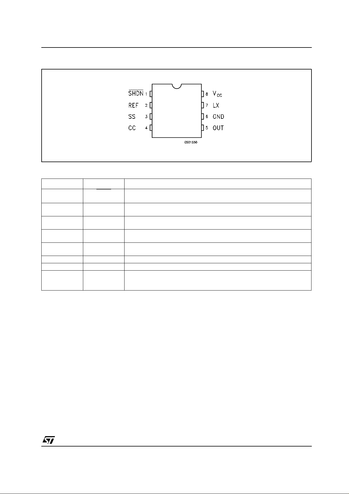
CONNECTION DIAGRAM (top view)
PIN DESCRIPTION
Pin N° Symbol Name and Function
1 SHDN
2 REF Reference Output Voltage: (1.25V): Bypass to GND with a capacitor that does not
3 SS Soft Start: a capacitor between SS and GND provides soft-start and short-circuit
4 CC Compensation Capacitor Input: externally compensates the outer (voltage)
5 OUT Output Voltage Sense Input: provides regulation of feedback sensing. Connect to
6 GND Ground
7 LX Switch Output. Drain of internal P-Channel Power MOSFET
8V
CC
Shutdown control (active low): If connected to GND the IC is in shutdown.
Connect to V
for normal operation (ON MODE)
CC
exceed 47nF
protections.
feedback loop. Connect to OUT with 330pF capacitor
5V output.
Supply Voltage Input. Bypass to GND with 1µF ceramic capacitance and large
value electrolytic capacitor in parallel. The 1µF capacitor must be as close as
possible to the GND and V
CC
pins
ST730A
3/9
Page 4
ST730A
ELECTRICALCHARACTERISTICS(VCC=5V,IO=0mA,TA=T
MIN
toT
,unlessotherwisespecified.)
MAX
Symbol Parameter Test Conditions Min. Typ. Max. Unit
Input Voltage 4 11 V
V
CC
V
Output Voltage VCC=6to11V IO=0 to 450mA 4.75 5 5.25 V
O
∆V
∆V
I
SUPPLY
I
SHDN
V
R
DS(on)
V
∆V
f
Line Regulation VCC= 5.2 to 11V 0.15 %/V
O
Load Regulatio IO= 0 to 450mA 0.005 %/mA
O
η Power Efficency I
Supply Current ON Mode
V
SHDN Input High Threshold 2 V
IH
SHDN Input Low Threshold 0.25 V
V
IL
=300mA 92 %
O
0.8
OFF Mode, SHDN
=0
0.3
Shutdown Input Leakage
Current
Under Voltage Lockout VCCFalling 2.7 3 V
LOCK
LX On Resistance ILX=500mA 0.5 Ω
LX Leakage Current VCC= 12V VLX=0V 1 µA
I
LX
Reference Voltage TA= 25°C 1.17 1.24 1.31 V
REF
Temperature Reference
REF
Drift
Switching Frequency B series
OSC
Compensation Pin
R
C
Impedance
C series
180
160
50 ppm/°C
200 220
7500 Ω
2.5
100
1 µA
280
KHz
mA
µA
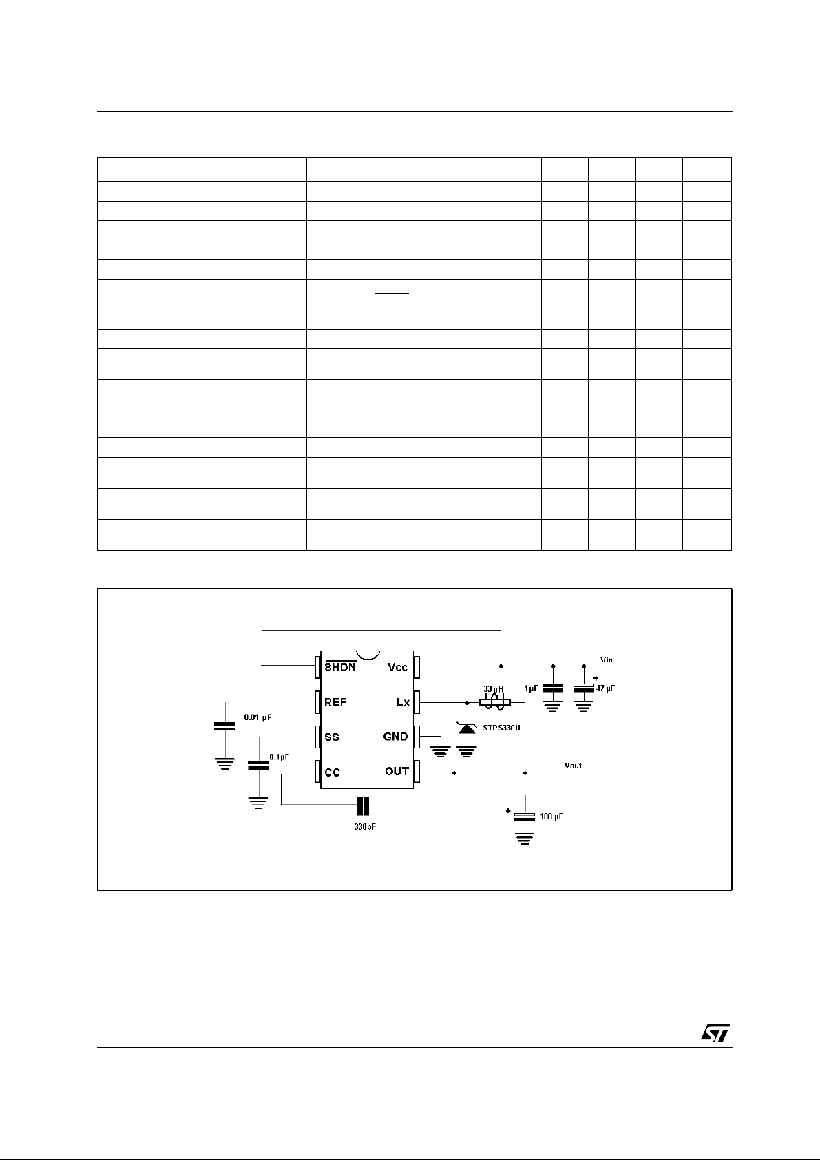
TYPICAL APPLICATION CIRCUIT
4/9
Page 5
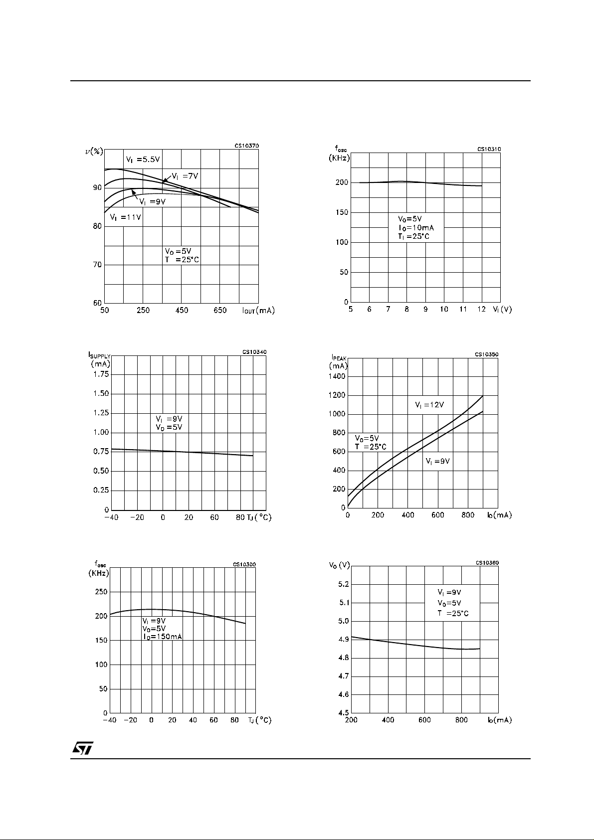
TYPICAL PERFORMANCE CHARACTERISTICS (unless otherwise specified Tj=25°C
ST730A
Figure1 : Ef fice nc y vs Output Current
Figure2 : Supply Current vs Temperature
Figure4 : Oscillator Frequency vs Input Voltage
Figure5 : Peak Inductor Current vs Output
Current
Figure3 : Oscillator Frequency vs Temperature
Figure6 : Output Voltage vs Output Current
5/9
Page 6
ST730A
V
11V,I
300mA
V
11V,I
300mA
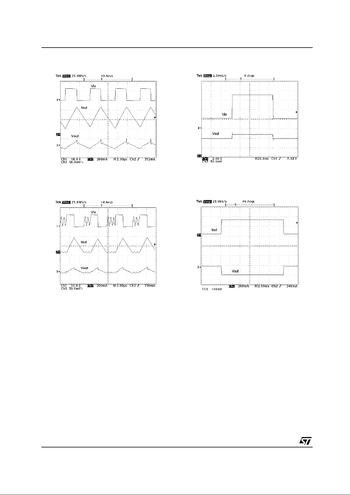
Figure7 : Sw itching Waveforms, Continuous
Conduction
=6Vto
I
=
O
Figure8 : Sw itching Waveforms, Discontinuous
Conduction
Figure9 : Line Transient
Figure10 : Load Transient
=6Vto
I
6/9
=
O
Page 7
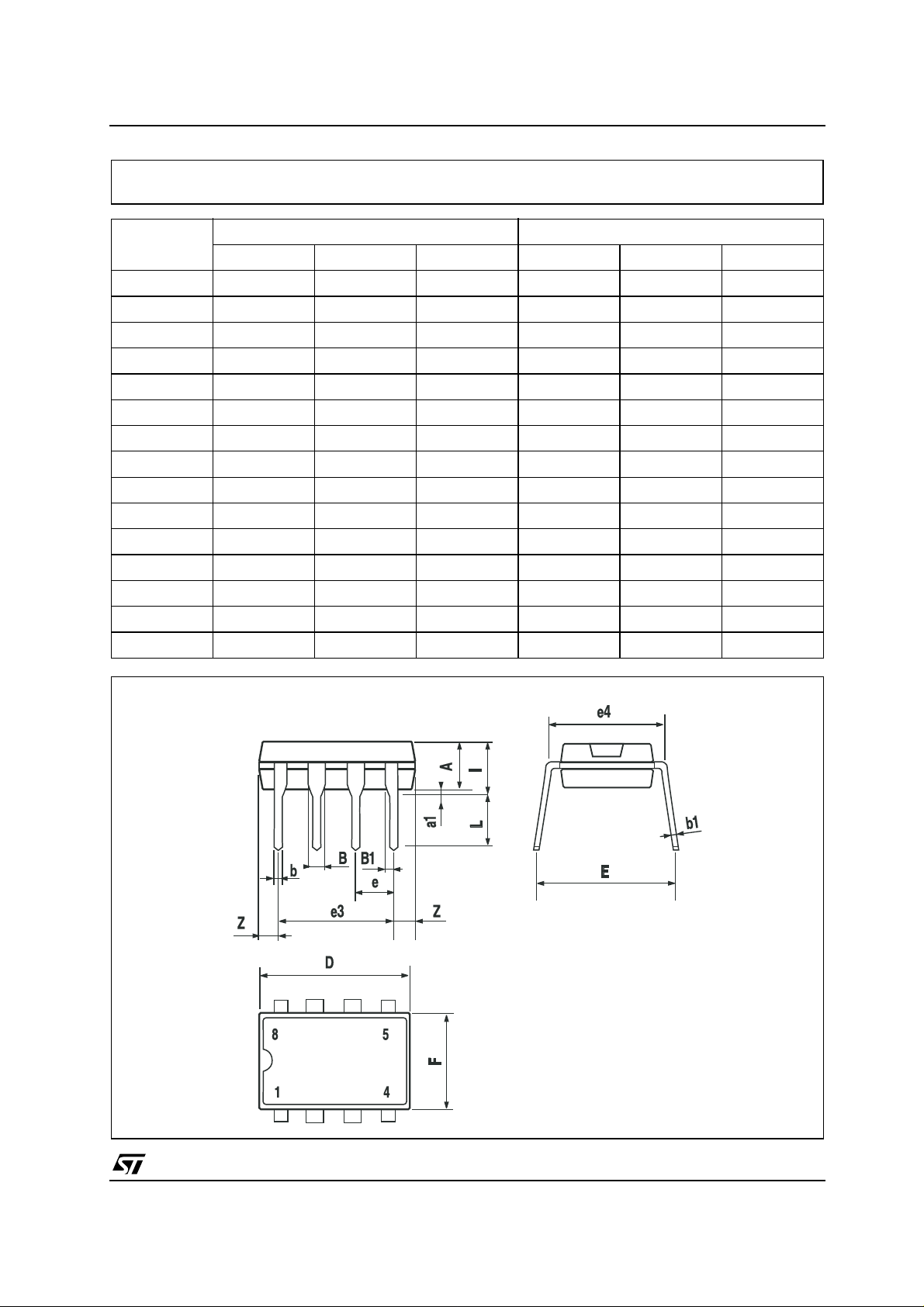
Plastic DIP-8 MECHANICAL DATA
ST730A
DIM.
MIN. TYP MAX. MIN. TYP. MAX.
A 3.3 0.130
a1 0.7 0.028
B 1.39 1.65 0.055 0.065
B1 0.91 1.04 0.036 0.041
b 0.5 0.020
b1 0.38 0.5 0.015 0.020
D 9.8 0.386
E 8.8 0.346
e 2.54 0.100
e3 7.62 0.300
e4 7.62 0.300
F 7.1 0.280
I 4.8 0.189
L 3.3 0.130
Z 0.44 1.6 0.017 0.063
mm. inch
P001F
7/9
Page 8
ST730A
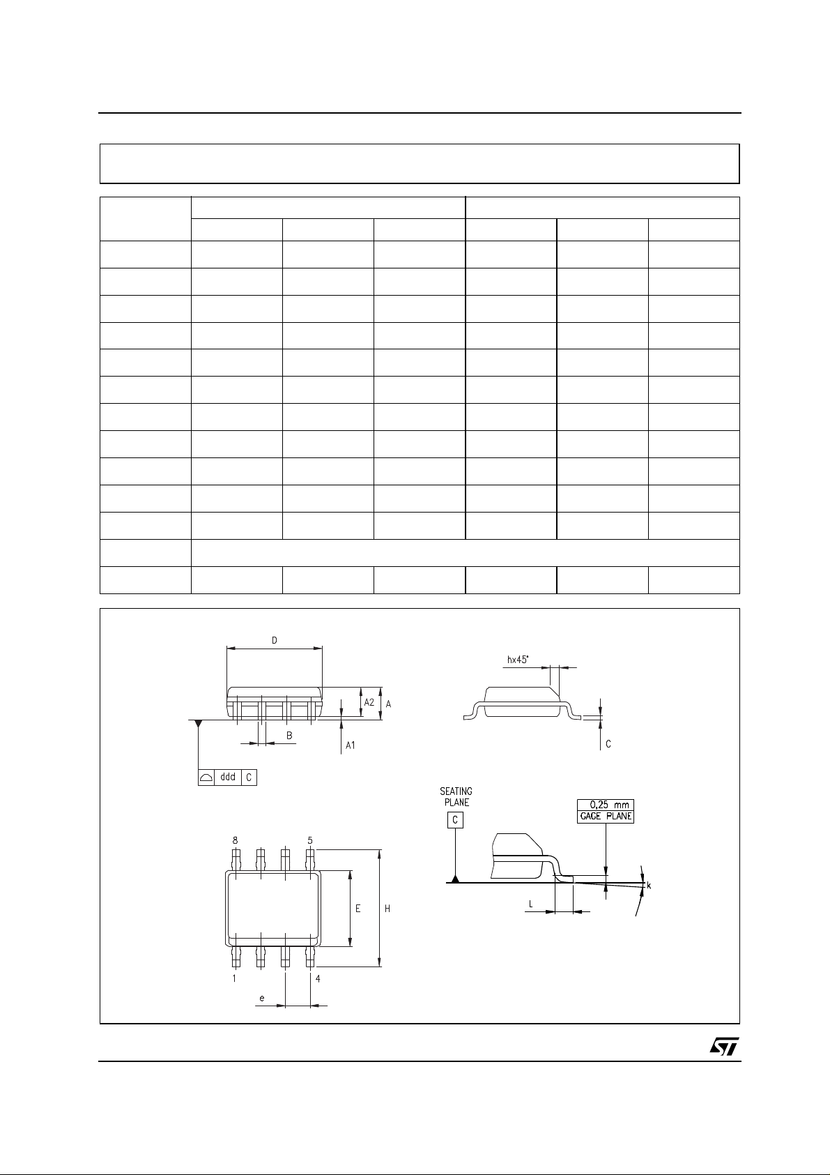
SO-8 MECHANICAL DATA
DIM.
A 1.35 1.75 0.053 0.069
A1 0.10 0.25 0.04 0.010
A2 1.10 1.65 0.043 0.065
B 0.33 0.51 0.013 0.020
C 0.19 0.25 0.007 0.010
D 4.80 5.00 0.189 0.197
E 3.80 4.00 0.150 0.157
e 1.27 0.050
H 5.80 6.20 0.228 0.244
h 0.25 0.50 0.010 0.020
L 0.40 1.27 0.016 0.050
k ˚ (max.)
ddd 0.1 0.04
MIN. TYP MAX. MIN. TYP. MAX.
mm. inch
8
8/9
0016023/C
Page 9

ST730A
o
rmation furnished is believed to be accurate and reliable. However, STMicroelectronics assumes no responsibility for the
sequences of u se of such inform ation nor for any in fring ement of p atents or o ther ri ghts of th ird p arties which may resul t fr o m
use. No license is granted by implication or otherwise under any patent or patent rights of STMicroelectronics. Specifications
ntioned in this publication are subject to change without notice. This publication supersedes and replaces all information
viously supplied. STMicroelectronics products are not authorized for use as critical components in life support devices or
tems without express written approval of STMicroelectronics.
ustralia - Brazil - Canada - China - Finland - France - Germany - Hong Kong - India - Israel - Italy - Japan - Malaysia - Malta - Morocco
© The ST logo is a registered trademark of STMicroelectronics
© 2003 STMicroelectronics - Printed in Italy - All Rights Reserved
STMicroelectronics GROUP OF COMPANIES
Singapore - Spain - Sweden - Switzerland - United Kingdom - United States.
© http://www.st.com
9/9
 Loading...