

Datasheet ST72T85A5Q6, ST72E85A5G0, ST7285C, ST7285A5CQ8, ST7285A5CQ6 Datasheet (SGS Thomson Microelectronics)
...Page 1
November 1997 1/117
R
Rev. 1.0
ST7285C
8-BIT MCU FOR RDS WITH 48K ROM, 3K RAM, ADC,
TWO TIMERS, TWO SPIs, I
2
C AND SCI INTERFACES
■
4.5V to 5.5V Supply Operating Range
■ Operates at 8.664MHz Oscillator Frequency for
RDS compatibility
■
Fully Static operation
■
-40°Cto+85°C Maximum Operating
Temperature Range
■
Run, Wait, Slow, Halt and RAM Retention
modes
■
User ROM: 48 Kbytes
■ Data RAM: 3 Kbytes, including 128 byte stack
■
80 pin plastic package
■
62 multifunctional bidirectional I/O lines:
– Programmable Interrupt inputs on some I/Os
– 8 Analog inputs
– EMI filtering
■
Two 16-bit Timers, each featuring:
– 2 Input Captures
– 2 Output Compares
– External Clock input (on Timer A)
– PWM and Pulse Generator modes
■ RDS Radio Data System Filter, Demodulator
and GBS circuits
■
8-bit Analog-to-Digital converter with 8 channel
analog multiplexer
■ Digital Watchdog
■
Two SPI Serial Peripheral Interfaces
■
SCI Serial Communications Interface
■ Full I
2
C multiple Master/Slave interface
■ 2KHz Beep signal generator
■
Master Reset and Power-On Reset
■
8-bit Data Manipulation
■ 63 Basic Instructions
■
17 main Addressing Modes
■
8 x 8 Unsigned Multiply Instruction
■ True Bit Manipulation
■ Complete Development Support on PC/DOS/
WindowsTMReal-Time Emulator
■
Full Software Package (C-Compiler, CrossAssembler, Debugger)
PQFP80
1
Page 2

2/117
Table of Contents
117
ST7285C . . . . . . . . . . . . . . . . . . . . . . . . . . . . . . . . . . . . . . . . . . . .1
1 GENERAL DESCRIPTION . . . . . . . ...............................................5
1.1 INTRODUCTION .........................................................5
1.2 PIN DESCRIPTION .......................................................6
1.3 MEMORYMAP .........................................................10
2 CENTRAL PROCESSING UNIT .................................................13
2.1 INTRODUCTION ........................................................13
2.2 CPU REGISTERS . . . . . . . . ...............................................13
3 CLOCKS, RESET, INTERRUPTS & POWER SAVING MODES ........................15
3.1 CLOCKSYSTEM........................................................15
3.1.1 General Description .................................................15
3.1.2 Crystal Resonator . . . . . . . . ..........................................15
3.1.3 Ceramic Resonator . . . ..............................................16
3.1.4 External Clock . . . . . . . ..............................................16
3.2 MISCELLANEOUS REGISTER . . . . . . . . . . . . . . . . . . . . . . . . . . . . . ................17
3.3 RESETS...............................................................18
3.3.1 Introduction . . . . . . . . ...............................................18
3.3.2 External Reset . . . . . . . . . . ...........................................18
3.3.3 Reset Operation . . . . . . . . . . . . . . . .....................................18
3.3.4 Power-on Reset . . . . . . . . . . . . . . . .....................................18
3.4 WATCHDOG TIMER SYSTEM (WDG) . . .....................................19
3.4.1 Introduction . . . . . . . . ...............................................19
3.4.2 Functional Description . . . ............................................19
3.4.3 Watchdog Register . . . ..............................................19
3.5 INTERRUPTS . . . . ......................................................20
3.6 POWER SAVING MODES .................................................22
3.6.1 SlowMode........................................................22
3.6.2 WaitMode ........................................................22
3.6.3 HaltMode.........................................................23
4 ON-CHIP PERIPHERALS . . . ...................................................24
4.1 I/OPORTS.............................................................24
4.1.1 Introduction . . . . . . . . ...............................................24
4.1.2 Generic I/O Features . . . . . . . . . . . . . . . . . . . . . . . . . . . . . . . . ................24
4.1.3 I/O Port Implementation . . . . . . . . . . . . ..................................27
4.2 SERIAL COMMUNICATIONS INTERFACE. . ..................................28
4.2.1 Introduction . . . . . . . . ...............................................28
4.2.2 Features . . . . . . . . . . . . . . . ...........................................28
4.2.3 Serial Data Format . .................................................28
4.2.4 Data Reception and Transmission. . . ...................................28
4.2.5 Receiver Muting and Wake-up Feature . . . . ..............................28
4.2.6 Baud Rate Generation . . . ............................................29
4.2.7 SCI Register Overview . . . ............................................29
4.3 16-BIT TIMER . . . . ......................................................35
4.3.1 Introduction . . . . . . . . ...............................................35
4.3.2 Counter . . . . ......................................................35
Page 3

3/117
Table of Contents
4.3.3 External Clock . . . . . . . ..............................................37
4.3.4 Input Capture . . . ...................................................39
4.3.5 Output Compare . . . . ...............................................40
4.3.6 Timer Registers . . . . . . . . . . . . . . . . . . . . . . . . . . . .........................43
4.4 SERIAL PERIPHERAL INTERFACE . . . . . . . . . . . . . . . . . . . . .....................45
4.4.1 Introduction . . . . . . . . ...............................................45
4.4.2 Features . . . . . . . . . . . . . . . ...........................................45
4.4.3 Functional Description . . . ............................................45
4.4.4 Signal Description . . . . . . . . ..........................................47
4.4.5 Master Out Slave In (MOSI). ..........................................47
4.4.6 Master In Slave Out (MISO) . ..........................................47
4.4.7 Serial Peripheral Control Register (SPCR) ...............................50
4.4.8 Serial Peripheral Status Register (SPSR) . . . . . ...........................51
4.4.9 Serial Peripheral Data I/O Register (SPDR) . . . . . .........................53
4.4.10Single Master And Multimaster Configurations . . . . ........................53
4.5 I2C BUS INTERFACE . . . . . . . . . . . . . . . . . . . . . . . . . . . .........................54
4.5.1 Introduction . . . . . . . . ...............................................54
4.5.2 General Features . . . . ...............................................54
4.5.3 Functional Description . . . ............................................54
4.5.4 EPROM/ROM I C COMPATIBILITY APPLICATION NOTE. . . . ...............56
4.5.5 Re giste r Desc ript ion .................................................57
4.5.6 I2C Stat e Machine: . . . ..............................................61
4.6 A /D CONVERTER (ADC) . .................................................64
4.6.1 Introduction . . . . . . . . ...............................................64
4.6.2 Fu nctio nal De scrip tion . . . ............................................64
4.6.3 Re giste r Desc ript ion .................................................65
4.7 RDS FILTER . . . ........................................................66
4.7.1 Fe atures . . . . . . . . . . . . . . . ...........................................66
4.7.2 Fu nctio nal De scrip tion . . . ............................................67
4.8 RDS DEMODULATOR . . . . . . . . . . . . . . . .....................................68
4.8.1 Fe atures . . . . . . . . . . . . . . . ...........................................68
4.8.2 Fu nctio nal De scrip tion . . . ............................................69
4.9 RDSG.B.S.............................................................72
4.9.1 Introduction . . . . . . . . ...............................................72
4.9.2 Fe atures . . . . . . . . . . . . . . . ...........................................72
4.9.3 Fu nctio nal De scrip tion . . . ............................................74
4.9.4 Ac quisition of Group and Block Synchronization . . . . .......................77
4.9.5 Application Tips . . . . . . . . . . . . . . . . . . . . . . . . . . . .........................77
4.9.6 Block Synchronization Software . . .....................................77
4.9.7 Error Correction s oftwar e . . . . . . . . . . . . . . . . . . . . . . . . . . . . . ................77
5SOFTWARE ................................................................78
5.1 S T7 ARCHITECTU RE . . . . . . . . . . . . . . . .....................................78
5.2 S T7 ADDRESSING MOD ES ...............................................78
5.3 S T7 INSTRUCT ION SET . .................................................83
6 EL ECT RICAL CHARACTERI STI CS. . . . . . . . . . . . ..................................86
6.1 A BSO LUT E M AXIMUM RATINGS. ..........................................86
6.2 P OWER CONSID ERATIONS . . . . ..........................................87
Page 4

4/117
Table of Contents
117
6.3 DC ELECTRICAL CHARACTERISTICS ......................................88
6.4 AC ELECTRICAL CHARACTERISTICS ......................................89
6.5 CONTROLTIMING ......................................................89
7 GENERAL INFORMATION . . . . . . . . . . ...........................................96
7.1 PACKAGE MECHANICAL DATA. . . . ........................................96
ST72E85
ST72T85 . . . . . . . . . . . . . . . . . . . . . . . . . . . . . . . . . . . . . . . . . . .97
1 GENERAL DESCRIPTION. . . ...................................................98
1.1 INTRODUCTION ........................................................98
1.2 PIN DESCRIPTION ......................................................99
1.3 MEMORYMAP.........................................................103
1.4 EPROM ERASURE .....................................................105
1.5 EPROM/R OM I C COMPATIBILITY APPLICATION NOTE.......................106
2 ELECTRICAL CHARACTERISTI CS. . . . .........................................107
2.1 ABSOLUTE MAXIMUM RATINGS. . . . . . ....................................107
2.2 POWER CONSIDERATIONS. . . ...........................................108
2.3 DC ELECTRICAL CHARACTERISTICS .....................................109
2.4 AC ELECTRICAL CHARACTERIS TICS. . . ...................................110
2.5 CONTROLTIMING......................................................110
3 GENERAL INFORMATION . . . . . . . . . . ..........................................117
3.1 PACKAGE MECHANICAL DATA. . . . .......................................117
Page 5
5/117
ST7285C
1 GENERAL DESCRIPTION
1.1 INTRODUCTION
The ST7285C HCMOS Microcontroller Unit is a
member of the ST7 family of Microcontrollers dedicated to car radio applications with RDS capability. The device is based on an industry-standard 8bit core and features an enhanced instruction set.
The device is normally operated at an 8.664MHz
oscillator frequency for RDS compatibility but,
thanks to the fully static design, operation is possible down to DC, when RDS functionality is not required. Under software control, theST7285C may
be placed in either WAIT, SLOW or HALT modes,
thus reducing power consumption. The enhanced
instruction set and addressing modes afford real
programming potential. In addition to standard 8bit data management, theST7285C features true
bit manipulation, 8x8 unsigned multiplication and
indirect addressing modes.
The device includes an on-chip oscillator, CPU,
ROM, RAM, 62 I/O lines and the following on-chip
peripherals: Analog-to-Digital converter (ADC),
two industry standard SPI serial interfaces, a Serial Communications Interface, an I2C interface, a
digital Watchdog Timer, two independent 16-bit
Timers, one featuring an External Clock Input, and
both featuring Pulse Generator capabilities, 2 Input Captures and 2 Output Compares. RDS Filter,
Demodulator and GBS circuitry for car radio applications is also included.
NOTE
:
FOR THIS DEVICE, SGS-THOMSON
CAN ONLY RECEIVE MOTOROLA S19 FORMAT
FOR ROM CODES.
Figure 1. ST7285C Block Diagram
*On EPROM or OTP versions only.
Power on Reset
PA0 - PA7
Pin 65..72
PB0 - PB7
Pin 73..80
OSCin
OSCout
RESET
V
PP
/ TEST
OSC
8 -BIT CORE
ALU
VR01735P
Internal
CLOCK
ADDRESSand DATA BUS
TimerA
PORT A
PORT B
A/D Converter
8
4
SPI B
PORT C
PC0 - PC7
Pin 5..12
SPI A
PORT D
I
2
C
SCI
8
RAM
3k
RDS
FILTER,DEMOD,GBS
8
8
8
TimerB
4
4
2
PD0 - PD7
Pin 13..20
2
PORT E
PE0 - PE7
Pin 25..32
8
PORT F
PF0 - PF7
Pin 33..40
8
PORT H
PORT G
PH0 - PH5
Pin 53..58
6
PG0 - PG7
Pin 45..52
8
ROMor EPROM*
48k
Watchdog
RDScomp
MPX
RDS fil
RDS ref
ARS
AINT
V
DD
V
SS
V
DDPVSSPVDDAVSSA
2
2
Page 6
6/117
ST7285C
1.2 PIN DESCRIPTION
All I/Os from Port A to Port D, as well as PH0, 1
and 2, feature alternate function compatibility.
Software selectable input pull-ups are available on
ports featuring interrupt capability (PC4, PC5,
PD4, PD5, PF0-PF3, PG3).
VSSA
VDDA
MPX
RDSREF
RDSFIL
RDSCOMP
PH5
PH4
PH3
PH2/RDSDATA
PH1/RDSCLKOUT
PH0/RDSQUAL
PG7
PG6
PG5
PG4
PG3
PG2
PG1
PG0
ARS
AINT
VDDP
VSSP
VSSP
VDDP
OSCOUT
OSCIN
PC0/MISO_B
PC1/MOSI_B
PC2/SCK_B
PC3/SS_B
PC4/OC2_B
PC5/OC1_B
PC6/IC2_B
PC7/IC1_B
PD0/MISO_A
PD1/MOSI_A
PD2/SCK_A
PD3/SS_A
PD4
PD5
PD6/SCL
PD7/SDA
RESET
VPP*/TEST
VDD
VSS
1
2
3
4
5
6
7
8
9 (I10)
10 (I10)
11
12
13
14
15
16
17 (I9)
18 (I9)
19
20
21
22
23
24
64
63
62
61
60
59
58
57
56
55
54
53
52
51
50
49
(I1) 48
47
46
45
44
43
42
41
80 79 78 77 76 75 74 73 72 71 70 69 68 67 66 65
25 26 27 28 29 30 31 32 37 38 39
40
PB7/BEEP/
CLKOUT
PB6/CLKEXT
PB5/OC2_A
PB4/OC1_A
PB3/IC2_A
PB2/IC1_A
PB1/RDI
PB0/TDO
PA7/AIN7
PA6/AIN6
PA5/AIN5
PA4/AIN4
PA3/AIN3
PA2/AIN2
PA1/AIN1
PA0/AIN0
PE0
PE1
PE2
PE3
PE4
PE5
PE6
PE7
PF0
PF1
PF2
PF3
PF4
PF5
PF6
PF7
33 34 35 36
*) On EPROM/OTPversions only
(I2)(I2)(I2)(I2)
Page 7
7/117
ST7285C
Pin Pin Name(s) Basic Function Alternate Function Remarks
1V
SSP
Ground for Output Buffers
-
This pin is connected to pin 41
2V
DDP
Power Supply for Output Buffers
This pin is connected to pin 42
3 OSCOUT Oscillator Output pin.
4 OSCIN Oscillator Input pin.
5 PC0/MISO_B I/O Port PC0
SPI B master in/slave
out data input/output
Alternate function or I/O. The I/O configuration
is software selectable as triggered input or
push pull output.
6 PC1/MOSI_B I/O Port PC1
SPI B Master Out/
Slave In Data Input/
Output
7 PC2/SCK_B I/O Port PC2 SPI B Serial Clock
8 PC3/SS_B I/O Port PC3 SPI B Slave Select
9 PC4/OC2_B I/O Port PC4
Output Compare 2
on Timer B
Alternate function or I/O. Software selectable
as triggered input, push pull output, or triggered interrupt input with pull up (Interrupt I10).
10 PC5/OC1_B I/O Port PC5
Output Compare 1
on Timer B
11 PC6/IC2_B I/O Port PC6
Input Capture 2
on Timer B
Alternate function or I/O. The I/O configuration
is software selectable as triggered input or
push pull output.
12 PC7/IC1_B I/O Port PC7
Input Capture 1
on Timer B.
13 PD0/MISO_A I/O Port PD0
SPI A Master In/Slave
Out Data Input/Output
14 PD1/MOSI_A I/O Port PD1
SPI A Master Out/
Slave In data Input/
Output
15 PD2/SCK_A I/O Port PD2 SPI A Serial Clock
16 PD3/SS_A I/O Port PD3 SPI A Slave Select
17 PD4 I/O Port PD4 - Software selectable as triggered input, push
pull output, open drain output or triggered interrupt input with pull up (Interrupt I9).
18 PD5 I/O Port PD5 19 PD6/SCL I/O Port PD6 I
2
C Serial Clock Alternate function or I/O. The I/O configuration
is software selectable as triggered input or
open drain output.
20 PD7/SDA I/O Port PD7 I
2
C Serial Data
21 RESET General Reset -
Bidirectional. An active low signal forces MCU
initialization. This event is the top priority nonmaskable interrupt. As an output, it can be
used to reset external peripherals.
22 TEST RESERVED -
Input. This pin MUST be tied directly to V
SS
during normal operation.
23 V
DD
Power Supply forall logic circuitry
Except for output buffers and pull-ups.
24 V
SS
Ground for all logic circuitry
-
25 PE0 I/O Port PE0 -
Software selectable as triggered input or push
pull output.
26 PE1 I/O Port PE1 27 PE2 I/O Port PE2 28 PE3 I/O Port PE3 29 PE4 I/O Port PE4 30 PE5 I/O Port PE5 31 PE6 I/O Port PE6 32 PE7 I/O Port PE7 -
Page 8
8/117
ST7285C
33 PF0 I/O Port PF0 -
Software selectable as triggered input, a push
pull output, open drain output, or triggered interrupt input with pull up (Interrupt I2).
34 PF1 I/O Port PF1 35 PF2 I/O Port PF2 36 PF3 I/O Port PF3 37 PF4 I/O Port PF4 -
Software selectable as a triggered input or as
a push pull output.
38 PF5 I/O Port PF5 39 PF6 I/O Port PF6 40 PF7 I/O Port PF7 -
41 V
SSP
Ground for Output Buffers.
- This pin is connected to pin 1.
42 V
DDP
Power Supply for Output Buffers
- This pin is connected to pin 2.
43 AINT Reserved - Must be tied to 5V
44 ARS Reserved - Must be tied to 5V
45 PG0 I/O Port PG0 -
Software selectable as triggered input or push
pull output.
46 PG1 I/O Port PG1 47 PG2 I/O Port PG2 -
48 PG3 I/O Port PG3 -
Software selectable as triggered input, a push
pull output, open drain output, or triggered interrupt input with pull up (Interrupt I1).
49 PG4 I/O Port PG4 -
Software selectable as triggered input or push
pull output. Note that PH0, 1, 2 offer alternate
function capabilities for test purposes.
50 PG5 I/O Port PG5 51 PG6 I/O Port PG6 52 PG7 I/O Port PG7 -
53
PH0/
RDSQUAL
I/O Port PH0 RDS Quality signal
54
PH1/
RDSCLKOUT
I/O Port PH1
RDS GBS Clock Out
signal
55
PH2/
RDSDATA
I/O Port PH2 RDS GBS Data signal
56 PH3 I/O Port PH3 -
Software selectable as triggered input or high
voltage (10V max) open drain output.
57 PH4 I/O Port PH4 58 PH5 I/O Port PH5 -
59 RDSCOMP RDS Comp Input signal
Used to feed theDemodulator froman external
filter when the internal filter is switched off.
60 RDSFIL
RDS Filtered Output
signal
Used for Demodulator test purposes.
61 RDSREF RDS Input Reference
62 MPX RDS input signal
63 V
DDA
Analog Power Supply
For RDS and ADC circuits
64 V
SSA
Analog Ground
65 PA0/AIN0 I/O Port PA0
Analog input to ADC
Alternate function or I/O. The I/O configuration
is software selectable as triggered input or
push pull output. Note that when a pin is used
as Analog input it must not be configured as an
output to avoid conflicts with the analog voltage to be measured.
66 PA1/AIN1 I/O Port PA1
67 PA2/AIN2 I/O Port PA2
68 PA3/AIN3 I/O Port PA3
69 PA4/AIN4 I/O Port PA4
70 PA5/AIN5 I/O Port PA5
71 PA6/AIN6 I/O Port PA6
72 PA7/AIN7 I/O Port PA7
Pin Pin Name(s) Basic Function Alternate Function Remarks
Page 9
9/117
ST7285C
73 PB0/TDO I/O Port PB0
SCI Transmit Data
Out
Alternate function or I/O. The I/O configuration
is software selectable as triggered input or
push pull output.
74 PB1/RDI I/O Port PB1 SCI Receive Data In
75 PB2/IC1_A I/O Port PB2
Input capture 1
on Timer A
76 PB3/IC2_A I/O Port PB3
Input capture 2
on Timer A
77 PB4/OC1_A I/O Port PB4
Output compare 1
on Timer A
78 PB5/OC2_A I/O Port PB5
Output compare 2
on Timer A
79 PB6/CLKEXT I/O Port PB6
External Clock on
Timer A
80
PB7/BEEP/
CLKOUT
I/O Port PB7 BEEP or CPU Clock.
This pin can be a push pull output delivering
the Beep signal (2KHz) or the CPU clock, according to the miscellaneous register settings.
Pin Pin Name(s) Basic Function Alternate Function Remarks
Page 10

10/117
ST7285C
1.3 MEMORY MAP
Table 1. Memory Map
Address Block Register name
Reset
Status
Remarks
0000h
0001h
0002h
0003h
Port A
Data Reg
Data Direction Reg
Not Used
Not Used
00h
00h
R/W Register
R/W Register
Absent
Absent
0004h
0005h
0006h
0007h
Port B
Data Reg
Data Direction Reg
Not Used
Not Used
00h
00h
R/W Register
R/W Register
Absent
Absent
0008h
0009h
000Ah
000Bh
Port C
Data Reg
Data Direction Reg
Option Reg
Not Used
00h
00h
--00----b
R/W Register
R/W Register
R/W Register
Absent
000Ch
000Dh
000Eh
000Fh
Port D
Data Reg
Data Direction Reg
Option Reg
Not Used
00h
00h
--00----b
R/W Register
R/W Register
R/W Register
Absent
0010h
0011h
0012h
0013h
Port E
Data Reg
Data Direction Reg
Not Used
Not Used
00h
00h
R/W Register
R/W Register
Absent
Absent
0014h
0015h
0016h
0017h
Port F
Data Reg
Data Direction Reg
Option Reg
Not Used
00h
00h
----0000b
R/W Register
R/W Register
R/W Register
Absent
0018h
0019h
001Ah
001Bh
Port G
Data Reg
Data Direction Reg
Option Reg
Not Used
00h
00h
----0---b
R/W Register
R/W Register
R/W Register
Absent
001Ch
001Dh
001Eh
001Fh
Port H
Data Reg
Data Direction Reg
Not Used
Not Used
00h
00h
R/W Register
R/W Register
Absent
Absent
0020h
Miscellaneous Reg-
ister
00h see register description
0021h
0022h
0023h
SPI A
Data I/O Reg
Control Reg
Status Reg
XXh
0xh
00h
R/W Register
R/W Register
Read Only Register
0024h WDG Watchdog register 7Fh see register description
0025h
0026h
0027h
SPI B
Data I/O Reg
Control Reg
Status Reg
XXh
0xh
00h
R/W Register
R/W Register
Read Only Register
Page 11

11/117
ST7285C
0028h
0029h
002Ah
002Bh
002Ch
002Dh
002Eh
I
2
C
CR: Control Register
SR1: Status Register 1
SR2: Status Register 2
CCR: Clock Control Register
OAR1: Own Address Register 1
OAR2: Own Address Register 2
DR: Data Register
00h
00h
00h
00h
00h
00h
00h
R/W Register
Read Only Register
Read Only Register
R/W Register
R/W Register
R/W Register
R/W Register
002Fh
0030h
RESERVED
0031h
0032h
0033h
0034h
0035h
0036h
0037h
0038h
0039h
003Ah
003Bh
003Ch
003Dh
003Eh
003Fh
Timer A
Control Reg2
Control Reg1
Status Reg
Input Capture1 High Register
Input Capture1 Low Register
Output Compare1 High Register
Output Compare1 Low Register
Counter High Register
Counter Low Register
Alternate Counter High Register
Alternate Counter Low RegisteR
Input Capture2 High Register
Input Capture2 Low Register
Output Compare2 High Register
Output Compare2 Low Register
00h
00h
XXh
XXh
XXh
XXh
XXh
FFh
FCh
00h
00h
XXh
XXh
XXh
XXh
R/W Register
R/W Register
Read Only Register
Read Only Register
Read Only Register
R/W Register
R/W Register
Read Only Register
Read Only Register
Read Only Register
Read Only Register
Read Only Register
Read Only Register
R/W Register
R/W Register
0040h RESERVED
0041h
0042h
0043h
0044h
0045h
0046h
0047h
0048h
0049h
004Ah
004Bh
004Ch
004Dh
004Eh
004Fh
Timer B
Control Reg2
Control Reg1
Status Reg
Input Capture1 High Register
Input Capture1 Low Register
Output Compare1 High Register
Output Compare1 Low Register
Counter High Register
Counter Low Register
Alternate Counter High Register
Alternate Counter Low Register
Input Capture2 High Register
Input Capture2 Low Register
Output Compare2 High Register
Output Compare2 Low Register
00h
00h
XXh
XXh
XXh
XXh
XXh
FFh
FCh
00h
00h
XXh
XXh
XXh
XXh
R/W Register
R/W Register
Read Only Register
Read Only Register
Read Only Register
R/W Register
R/W Register
Read Only Register
Read Only Register
Read Only Register
Read Only Register
Read Only Register
Read Only Register
R/W Register
R/W Register
0050h
0051h
0052h
0053h
0054h
0055h
0056h
0057h
SCI
SCI Prescaler
SCSR: Status Register
SCDR: Data Register
SCBRR: Baud Rate Register
SCCR1: Control Register 1
SCCR2: Control Register 2
PSCBRR: Receive Baud Rate Reg
Reserved
PSCBRT: Transmit Baud Rate Reg
1100000xb
XXh
00x----xb
XXh
00h
00h
---
00h
Read Only Register
R/W Register
R/W Register
R/W Register
R/W Register
R/W Register
Reserved ST use
R/W Register
0058h RESERVED
0059h RESERVED
005Ah
005Bh
RDS Filter
RDS FI1
RDS FI2
R/W Register
R/W Register
Address Block Register name
Reset
Status
Remarks
Page 12
12/117
ST7285C
005Ch
005Dh
005Eh
005Fh
RDS Demodulator
RDS DE1
RDS DE2
RDS DE3
RDS DE4
see register description
0060h
0061h
0062h
0063h
0064h
0065h
0066h
0067h
0068h
0069h
006Ah
006Bh
006Ch
006Dh
006Eh
006Fh
RDS GBS
SR0 -Shift Reg 0
SR1 -Shift Reg 1
SR2 -Shift Reg 2
SR3 -Shift Reg 3
SY0 -Polynomial Reg 0
SY1 -Polynomial Reg 1
GS_CNT Count Reg
GS_INT Interrupt Reg
DR0 -RDSDAT Reg 0
DR1 -RDSDAT Reg 1
DR2 -RDSDAT Reg 2
DR3 -RDSDAT Reg 3
QR0 -QUALITY Reg 0
QR1 -QUALITY Reg 1
QR2 -QUALITY Reg 2
QR3 -QUALITY Reg 3
see register description
0070h
0071h
ADC
Data Reg
Control/Status Reg
XXh
00h
Read Only Register
R/W Register
0072h to
007Fh
RESERVED
0080h to
0BFFh
0C00h to
0C7Fh
RAM 3K Bytes
of which
STACK 128 Bytes
User variables and subroutine nesting
0C80h to
3FFFh
RESERVED
4000h to
FFDFh
ROM 48K bytes
(49120 bytes)
User application code and data
FFE0h to
FFFFh
User vectors Interrupt and Reset Vectors
Address Block Register name
Reset
Status
Remarks
Page 13
13/117
ST7285C
2 CENTRAL PROCESSING UNIT
2.1 INTRODUCTION
The CPU has a full 8-bit architecture. Six internal
registers allow efficient 8-bit data manipulation.
The CPU is capable of executing 63 basic instructions and features 17 main addressing modes.
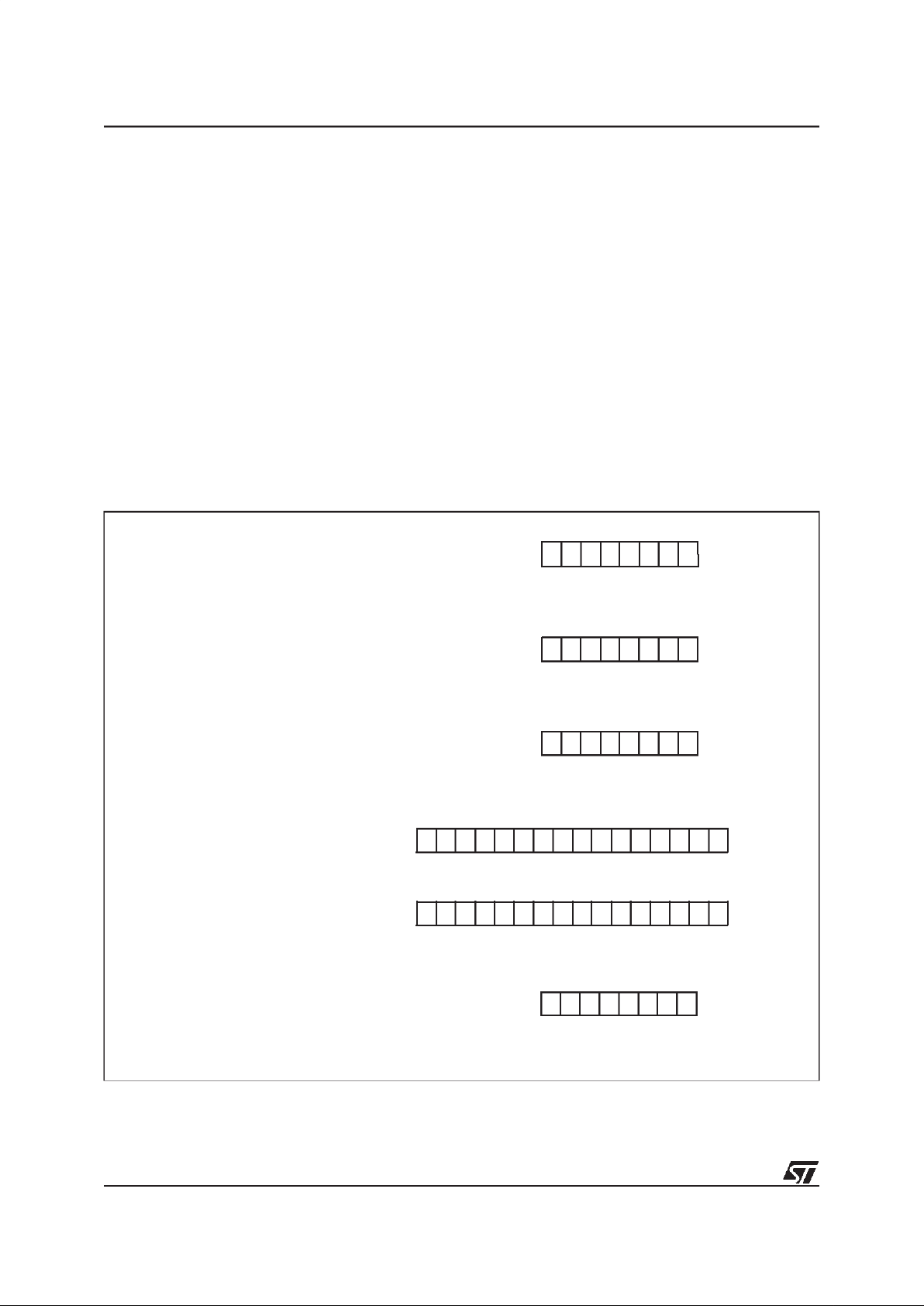
2.2 CPU REGISTERS
The 6 CPU registers are shown in the programming model inFigure 2. Following an interrupt, all
registers except Y are pushed onto the stack in the
order shown in Figure 3. They are popped from
stack in the reverse order.
Accumulator (A). The Accumulator is an 8-bit
general purpose register used to hold operands
and the results of the arithmetic and logic calculations as well as data manipulations.
Index Registers (X and Y).These 8-bit registers
are used to create effective addresses or as temporary storage areas for data manipulation. The
Cross-Assembler generates a PRECEDE instruction (PRE) to indicate that the following instruction
refers to the Y register. The Y register is never automatically stacked. Interrupt routines must push
or pop it by using the PUSH and POP instructions.
Program Counter (PC).The program counter is a
16-bit register containing the address of the next
instruction to be executed by the CPU.
Figure 2. Organization of Internal CPU Registers
ACCUMULATOR:
X INDEX REGISTER:
Y INDEX REGISTER:
PROGRAM COUNTER:
STACKPOINTER:
CONDITION CODE REGISTER:
X = Undefined
RESET VALUE:
70
XXXXXXXX
RESET VALUE:
70
XXXXXXXX
RESET VALUE:
70
XXXXXXXX
15
70
RESET VALUE = DEVICE DEPENDENT,SEE MEMORY MAP
RESET VALUE:
70
XXXXXXXX
15
70
RESET VALUE = DEVICE DEPENDENT,SEE MEMORY MAP
Page 14
14/117
ST7285C
CPU REGISTERS(Cont’d)
Stack Pointer (SP) The Stack Pointer is a 16-bit
register. Since the stack size can vary from device
to device, the appropriate number of most significant bits are forced so as to map the stack as defined in the Memory Map. The number of least significant digits thus available tothe user will depend
on the stack size, for example in the case of a 128
byte stack, 7 bits will be available whereas in the
case of a64 byte stack, only 6 bits will beavailable.
The stack is used to save the CPU context during
subroutine calls or interrupts. The user may also
directly manipulate the stack by means of the
PUSH and POP instructions.
Following an MCU Reset, or after a Restore following a Reset Stack Pointer instruction (RSP),
the StackPointer is set to point to thehighest location in the stack. It is then decremented after data
has been pushed onto the stack and incremented
after data is popped from the stack. When the lower limit is exceeded, the Stack Pointer wraps
around to the stack upper limit. The previously
stored information is then overwritten and therefore lost. The upper and lower limits of the stack
area are shown in the Memory Map.
A subroutine call occupies two locations and an interrupt five locations in the stack area.
Condition Code Register (CC) The Condition
Code register is a 5-bit register which indicates the
result of the instruction just executed as wellas the
state of the processor. These bits can be individually tested by a program and specified action taken
as a result of their state. The following paragraphs
describe each bit of the CC register in turn.
Half carry bit (H)The H bit is set to 1 when acarry
occurs between bits 3 and 4 of the ALU during an
ADD or ADC instruction. The H bit is useful in BCD
arithmetic subroutines.
Interrupt mask (I) When the I bit is set to 1, all interrupts except the TRAP software interrupt are
disabled. Clearing this bit enables interrupts to be
passed to the processor core. Interrupts requested
while I is set are latched and can be processed
when I is cleared (only one interrupt request per interrupt enable flag can be latched).
Negative (N)
When set to 1, this bit indicates that
the result of the last arithmetic, logical or data manipulation is negative (i.e. the most significant bit is
a logic 1).
Zero (Z)
When set to 1, this bit indicates that the
result of the last arithmetic, logical or data manipulation is zero.
Carry/Borrow (C) When set, C indicates that a
carry or borrow out of the ALU occured during the
last arithmetic operation. This bit is also affected
during execution of bit test, branch, shift, rotate
and store instructions.
Figure 3. Stacking Order
INCREASING
MEMORY
UNSTACK
ACCUMULATOR
X INDEX REGISTER
PCH
PCL
(PUSH)
DECREASING
MEMORY
111
VR000074
07
ADDRESSES
ADDRESSES
STACK
(POP)
CONDITION CODE
RETURN
INTERRUPT
Page 15
15/117
ST7285C
3 CLOCKS, RESET, INTERRUPTS & POWER SAVING MODES
3.1 CLOCK SYSTEM
3.1.1 General Description
The MCU accepts either a Crystal or Ceramic resonator, or an external clock signal to drive the internal oscillator. The internal clock (CPU CLK running at f
CPU
) is derived from the external oscillator
frequency (f
OSC).
The external Oscillator clock is
first divided by 2, and an additional division factor
of 2, 4, 8, or 16 can be applied, in Slow Mode, to
reduce the frequency of the CPU clock (see
note 1); this clock signal is also routed to the onchip peripherals. The CPU clock signal consists of
a square wave with a duty cycle of 50%.
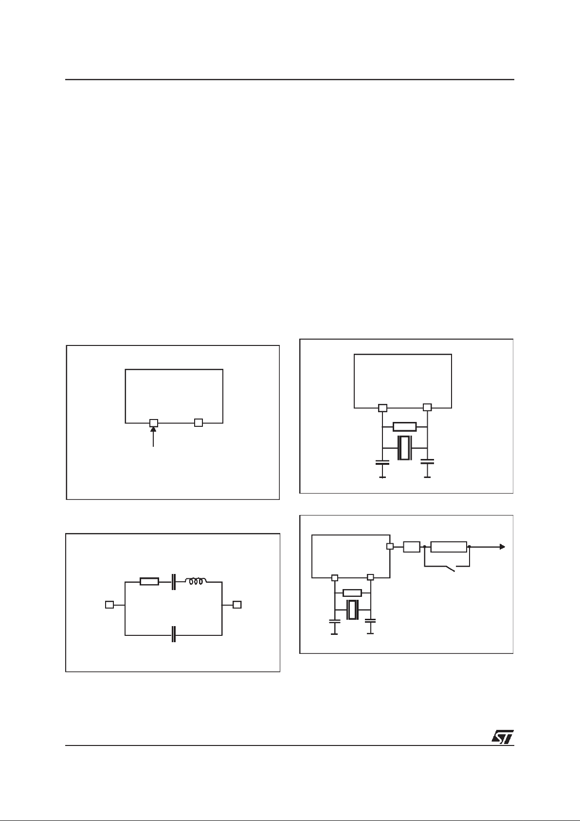
Figure 4. External Clock Source Connections
Figure 5. Equivalent Crystal Circuit
3.1.2 Crystal Resonator
The internal oscillator is designed to operate with
an AT-cut parallel resonant quartz crystal resonator in the frequency range specified for f
osc
.The
circuit shown in Figure 6 is recommended when
using a crystal, andTable 2 lists the recommended capacitance and feedback resistance values.
The crystal and associated components should be
mounted as close as possible to the input pins in
order to minimize output distortion and start-up
stabilisation time.
Use of an external CMOS oscillator is recommended when crystals outside the specified frequency ranges are to be used.
Figure 6. Crystal/Ceramic Resonator
Figure 7. Clock Prescaler Block Diagram
Note 1: Additional division factor of CPU clock is only available on L5/L6.
OSC
in
OSC
out
EXTERNAL
CLOCK
NC
OSC
in
OSC
out
R
S
L
1
C
1
C
0
OSC
in
OSC
out
C
OSCin
C
OSCout
R
P
OSC
in
OSC
out
C
OSCin
C
OSCout
R
P
%2 %2,4,8,16
CPUCLK
to CPU and
Peripherals
Page 16
16/117
ST7285C
CLOCK SYSTEM (Cont’d)
3.1.3 Ceramic Resonator
A ceramic resonator may be used as an alternative to a crystal in low-cost applications. The circuit
shown in Figure 6 is recommended when using a
ceramic resonator. Table 3 lists the recommended
feedback capacitance and resistance values. The
manufacturer of the particular ceramic resonator
being considered should be consulted for specific
information.
Table 2. Recommended Values for Crystal
Resonator
3.1.4 External Clock
An external clock may be applied to the OSCin input with the OSCout pin not connected, as shown
on Figure 4. The t
OXOV
and t
ILCH
specifications do
not apply when using an external clock input. The
equivalent specification of the external clock
source should be used instead of t
OXOV
or t
ILCH
.
See CONTROL TIMING SECTION.
Table 3.Recommended Values for Ceramic
Resonator
Figure 8. Timing Diagram for Internal CPU Clock Frequency transistions
2MHz 4MHz 8MHz Unit
R
SMAX
400 75 60 Ω
C
0
5 7 10 pF
C
1
81215fF
C
OSCin
15-40 15-30 15-25 pF
C
OSCout
15-30 15-25 15-20 pF
R
P
10 10 10 MΩ
Q304060
10
3
2-8MHz Unit
R
SMAX
10 Ω
C
0
40 pF
C
1
4.3 pF
C
OSCin
30 pF
C
OSCout
30 pF
R
P
1-10 MΩ
Q 1250
MISCELLANEOUS REGISTER
00 10
1
10
VR02062B
New frequency
requested
New frequency
active when
f
OSC
/4 & f
OSC
/8 = 0
Normalmode
active
Normalmode
requested
PSM1:PSM0
SMS
f
OSC
/2
f
OSC
/4
f
OSC
/8
f
CPU
Page 17
17/117
ST7285C
3.2 MISCELLANEOUS REGISTER
The Miscellaneous register allows one to select
the SLOW operating mode and to set the clock division prescaler factor. Bits 3 and 4 allow one to
set PB7 functionality (I/O, CPU Clock o/p or Beep
signal o/p), while bits 6 and 7 determine the signal
conditions which will trigger an interrupt request on
I/O pins having interrupt capability.
Register Address: 0020h — Read/Write
Reset Value: 00h
b7, b6 -
EI1, EI0
:
External Interrupt Option
0 0 - Negative edge and low level (Reset state)
1 0 - Negative edge only
0 1 - Positive edge only
1 1 - Positive and negative edge
This selection applies globally to the four external
interrupts: I1, I2, I9 and I10.
b6 and b7 can be written only when the Interrupt
Mask (I) of the CC (Condition Code) register is set
to 1.
b5- Reserved
b4, b3 - SK1, CK0
:
Clock/Beep Output
0 0 - I/O port (Reset state)
1 0 - I/O port
0 1 - CPU Clock output to pin PB7
1 1 - 2KHz Beep signal output to pin PB7
(at 8.664 MHz oscillator frequency)
b2, b1 - SM1,SM0:
CPU clock prescaler for Slow
Mode
0 0 - Oscillator frequency / 4
1 0 - Oscillator frequency / 8
0 1 - Oscillator frequency / 16
1 1 - Oscillator frequency / 32
b0 - SMS:
Slow Mode Select
0- Normal mode - Oscillator frequency / 2
(Reset state)
1- Slow mode (Bits b1 and b2 define the prescaler
factor)
70
EI1 EI0 b5 SK1 CK0 SM1 SM0 SMS
Page 18
18/117
ST7285C
3.3 RESETS
3.3.1 Introduction
There are four sources of Reset:
– RESET pin (external source)
– Power-On Reset (Internal source)
– WATCHDOG (Internal Source)
The Reset Service Routine vector is located at ad-
dress FFFEh-FFFFh.
3.3.2 External Reset
The RESET pin is both an input and an open-drain
output with integrated pull up resistor. When one
of the internal Reset sources is active, the Reset
pin is driven low to reset the whole application.
3.3.3 Reset Operation
The duration of the Reset condition, which is also
reflected on the output pin, is fixed at4096 internal
CPU Clock cycles. A Reset signal originating from
an external source must have a duration of at least
1.5 internal CPU Clock cycles in order to be recognised. At the end of the Power-On Reset cycle, the
MCU may be held in the Reset condition by an External Reset signal. The RESET pin may thus be
used to ensure VDDhas risen to a point where the
MCU can operate correctly before the User program is run. Following a Reset event, or after exit-
ing Halt mode, a 4096 CPU Clock cycle delay period is initiated in order to allow the oscillator to
stabilise and to ensure that recovery has taken
place from the Reset state.
During the Reset cycle, the device Reset pin acts
as an output that is pulsed low for 3 machine cycles (6 oscillator cycles). In its high state, an internal pull-up resistor of about 300KΩ is connected to
the Reset pin. This resistor can be pulled low by
external circuitry to reset the device.
3.3.4 Power-on Reset
This circuit detects the ramping up of VDD,and
generates a pulse thatis used to reset the application (at approximately VDD= 2V).
Power-On Reset is designed exclusively to cope
with power-up conditions, and should not be used
in order to attempt to detect a drop in the power
supply voltage.
Caution:
to re-initialize the Power-On Reset, the
power supply must fall below approximately 0.8V
(Vtn), prior to rising above 2V. If this condition is
not respected, on subsequent power-up the Reset
pulse may not be generated. An external pulse
may be required to correctly reactivate the circuit.
Figure 9. Reset Block Diagram
VDD
COUNTER
RESET
to ST7
VR2062C
300K
WATCHDOG RESET
OR DLPSS
RESET
OSCILLATOR
SIGNAL
INTERNAL
RESET
Page 19
19/117
ST7285C
3.4 WATCHDOG TIMER SYSTEM (WDG)
3.4.1 Introduction
The Watchdog timer is used to detect the occurence of a software fault, usually generated by
external interference or by unforeseen logical conditions, which causes the application program to
abandon its normal sequence. The Watchdog circuit generates an MCU reset on expiry of a programmed time period, unless the program refreshes the counter’s contents before it is decremented
to zero.
3.4.2 Functional Description
The counter is decremented every 12,288 machine cycles, and the length of the timeout period
can be programmed by the user in 64 increments,
ranging from 12,288 machine cycles to 786,432
machine cycles, depending on the value loaded in
bits 0-5 of the Watchdog register. The application
program must be written so that the Watchdog
register is reloaded at regular intervals during normal operation.
The Watchdog is not activated automatically on
Reset, and must be activated by the user program
if required. Once activated it cannot be disabled,
save by a Reset.
During the Reset cycle, the device Reset pin acts
as an output that is pulsed low for 3 machine cycles (6 oscillator cycles). In its high state, an internal pull-up resistor of about 100KΩis connected to
the Reset pin.
This resistor can be pulled low by external circuitry
to reset the device.
The Watchdog delay time is defined by bits 5-0 of
the Watchdog register; bit 6 must always be set in
order to avoid generating an immediate reset.
Conversely, this can be used to generate a software reset (bit 7 = 1, bit 6 = 0).
Once bit 7 is set, it cannot be cleared by software:
i.e. the Watchdog cannot be disabled by software
without generating a Reset. The Watchdog timer
mustbe reloaded before bit 6 is decremented to ”0”
to avoid a Reset. Following a Reset, the Watchdog
register will contain 7Fh (bits 0-6 = 1, bit 7 = 0).
If the Watchdog is activated, the HALT instruction
will generate a Reset.
If the circuit is not used as a Watchdog (i.e. bit 7 is
never set), bits 6 to 0 may be used as a simple 7bit timer, for instance as a real time clock. Since no
interrupt will be generated under these conditions,
the Watchdog register must be monitored by software.
3.4.3 Watchdog Register
Register Address: 0024h — Read/Write
Reset Value: 0111 1111 (7Fh)
b7 = WDGA: Activation bit (is active if set)
b6-0 =
T6-T0
: 7-bit timer counter (Msb to Lsb)
Table 4. Watchdog Timing (f
OSC
= 8 MHz)
70
WDGA T6 T5 T4 T3 T2 T1 T0
WDG Register initial
value
WDG timeout period (ms)
FF 197
C0 3
Page 20
20/117
ST7285C
3.5 INTERRUPTS
A list of interrupt sources is given inTable 5below,
together with relevant details for each source. Interrupts are serviced according to their order ofpriority, starting with I0, which has the highest priority, and so to I11, which has the lowest priority.
The following list describes the origins for each interrupt level:
– I0 connected to Software Interrupt (TRAP)
– I1 connected to Port G3
– I2 connected to Port F0, F1, F2, F3
– I3 connected to SPI A
– I4 connected to Timer A
– I5 connected to GBS interrupt
– I6 connected to Timer B
– I7 connected to SPI B
– I8 connected to SCI
– I9 connected to Ports D4, D5
– I10 connected to Ports C4, C5
– I11 connected to I2C
Exit from HALT mode may only be triggered by an
External Interrupt on one of the following ports:
C4(I10), C5(I10), D4(I9), D5(I9), F0(I2), F1(I2),
F2(I2), F3(I2) and G3(I1).
If more than one input pin of a group connected to
the same interrupt line is selected simultaneously,
these will be logically ORed.
Table 5. Interrupt Mapping
Interrupt
source
Vector
Address
Interrupts Register
Flag
name
CPU
interrupts
- FFFEh-FFFFh Reset N/A N/A RESET
I0 FFFCh-FFFDh Software N/A N/A TRAP
I1 FFFAh-FFFBh Ext. Interrupt (Port G3) N/A N/A INT1
I2 FFF8h-FFF9h Ex. Interrupt (Ports F0, F1, F2, F3) N/A N/A INT2
I3 FFF6h-FFF7h Transfer Complete SPI A Status SPIF1_A SPI_A
“ “ Mode Fault “ MODF1_A “
I4 FFF4h-FFF5h Input Capture 1 Timer A Status ICF1_A TIMER_A
“ “ Output Compare 1 “ OCF1_A “
“ “ Input Capture 2 “ ICF2_A “
“ “ Output Compare 2 “ OCF2_A “
“ “ Timer Overflow “ TOF_A “
I5 FFF2h-FFF3h RDS Block Interrupt. RDS GRP
VSI
CNI
GBS
I6 FFF0h-FFF1h Input Capture 1 Timer B Status ICF1_B TIMER_B
“ “ Output Compare 1 “ OCF1_B “
“ “ Input Capture 2 “ ICF2_B “
“ “ Output Compare 2 “ OCF2_B “
“ “ Timer Overflow “ TOF_B “
I7 FFEEh-FFEFh Transfer Complete SPI B Status SPIF2_B SPI_B
“ “ Mode Fault “ MODF1_B “
I8 FFECh-FFEDh Transmit Buffer Empty SCI Status TDRE SCI
“ “ Transmit Complete “ TC “
“ “ Receive Buffer Full “ RDRF “
“ “ Idle Line Detect “ IDLE “
“ “ Overrun “ OR “
I9 FFEAh-FFEBh Ext. Interrupt (Ports D4,D5) N/A N/A INT9
I10 FFE8h-FFE9h Ext. Interrupt (Port C4, C5) N/A N/A INT10
I11 FFE6h-FFE7h Byte Transmission Finished I
2
C Status BTF I2C
“ “ Bus Error “ BERR I2C
“ “ Stop Detection “ SSTOP I2C
Page 21
21/117
ST7285C
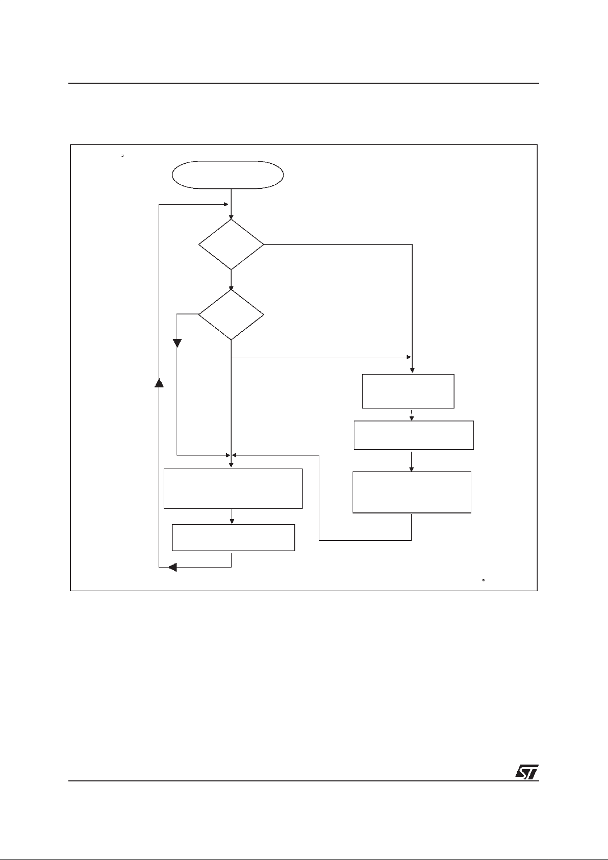
INTERRUPTS (Cont’d)
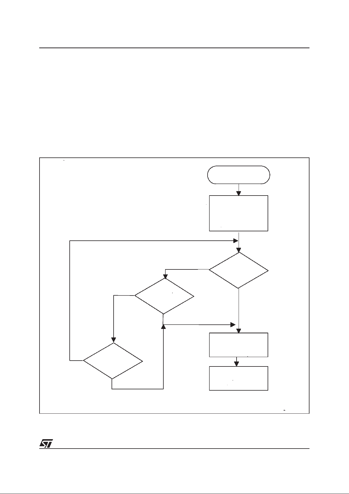
Figure 10. Interrupt Processing Flowchart
Note 1. See Table 5 . Interrupt Mapping
FROM RESET
TRAP
FETCH NEXT
INSTRUCTION
OF APPROPRIATE INTERRUPT
SERVICEROUTINE
EXECUTE INSTRUCTION
PUSH
PC,X,A,CC
SET I BIT TO 1
VR01172B
N
Y
LOAD PC
WITH APPROPRIATE
INTERRUPT VECTOR
(1)
I BIT = 1
N
Y
ONTO STACK
Page 22
22/117
ST7285C
3.6 POWER SAVING MODES
3.6.1 Slow Mode
The following Power Saving mode may be selected by setting the relevant bits in the Miscellaneous
register as detailed in Section3.2.
In Slow Mode, the oscillator frequency can be divided by 4, 8, 16 or 32 rather than by 2. The CPU
and peripherals are clocked at this lower frequency, and therefore the RDS filter cannot operate
correctly in this mode. SLOW mode is used to reduce power consumption, and enables the user to
adapt clock frequency to available supply voltage.
3.6.2 Wait Mode
WAIT mode places the MCU in a low power consumption mode by stopping the CPU. All peripherals remain active. During WAIT mode, the I bit (CC
Register) is cleared, so as to enable all interrupts.
All other registers and memory remain unchanged. The MCU will remain in WAIT mode until
an Interrupt or Reset occurs, whereupon the Program Counter branches to the starting address of
the Interrupt or Reset Service Routine.
Refer to Figure 11 below.
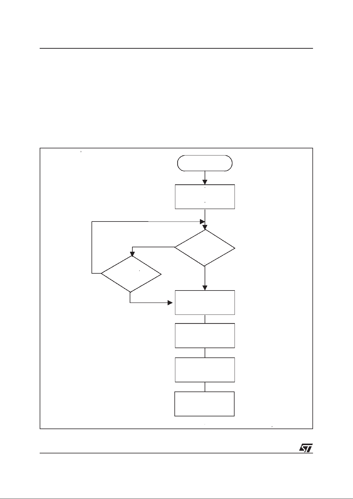
Figure 11. Wait Mode Flow Chart
WAIT
WAIT
Y
VR02062D
N
Y
Y
N
EXTERNAL
INTERRUPT
RESET
RESTART
PROCESSORCLOCK
FETCHRESET
VECTOROR
SERVICEINTERRUPT
PERIPHERAL
INTERRUPT
N
ACTIVE OSCILLATOR
AND PERIPHERALS
CLOCKSACTIVE
PROCESSORCLOCK
STOPPED
Page 23
23/117
ST7285C
POWER SAVING MODES(Cont’d)
3.6.3 Halt Mode
The HALT instruction places the MCU in its lowest
power consumption mode. In HALT mode the internal oscillator is turned off, causing all internal
processing to be halted. During HALT mode, the I
bit in the CC Register is cleared so as to enable
External Interrupts.
All other registers and memory remain unaltered
and all Input/Output lines remain unchanged. This
state will endure until an External Interrupt (I1, I2,
I9, I10) or a Reset is generated, whereupon the internal oscillator is restarted. A delay of 4096 CPU
clock cycles is initiated prior to restarting the application, in order to allow the oscillator to stabilize.
The External Interrupt or Reset causes the Program Counter to be set to the address of the corresponding Interrupt or Reset Service Routine.
Figure 12. Halt Mode Flow Chart
N
Y
VR02062E
N
EXTERNAL
INTERRUPT
WAIT
HALT
Y
STOP OSCILLATOR
ANDALL CLOCKS
CLEARI-BIT
RESET
OSCILLATOR
IN SLOW MODE
TURN ON
OSCILLATOR
WAIT FOR 4096 CPU
CLOCK TIME DELAY
FETCH RESET
VECTOROR
SERVICEINTERRUPT
Page 24

24/117
ST7285C
4 ON-CHIP PERIPHERALS
4.1 I/O PORTS
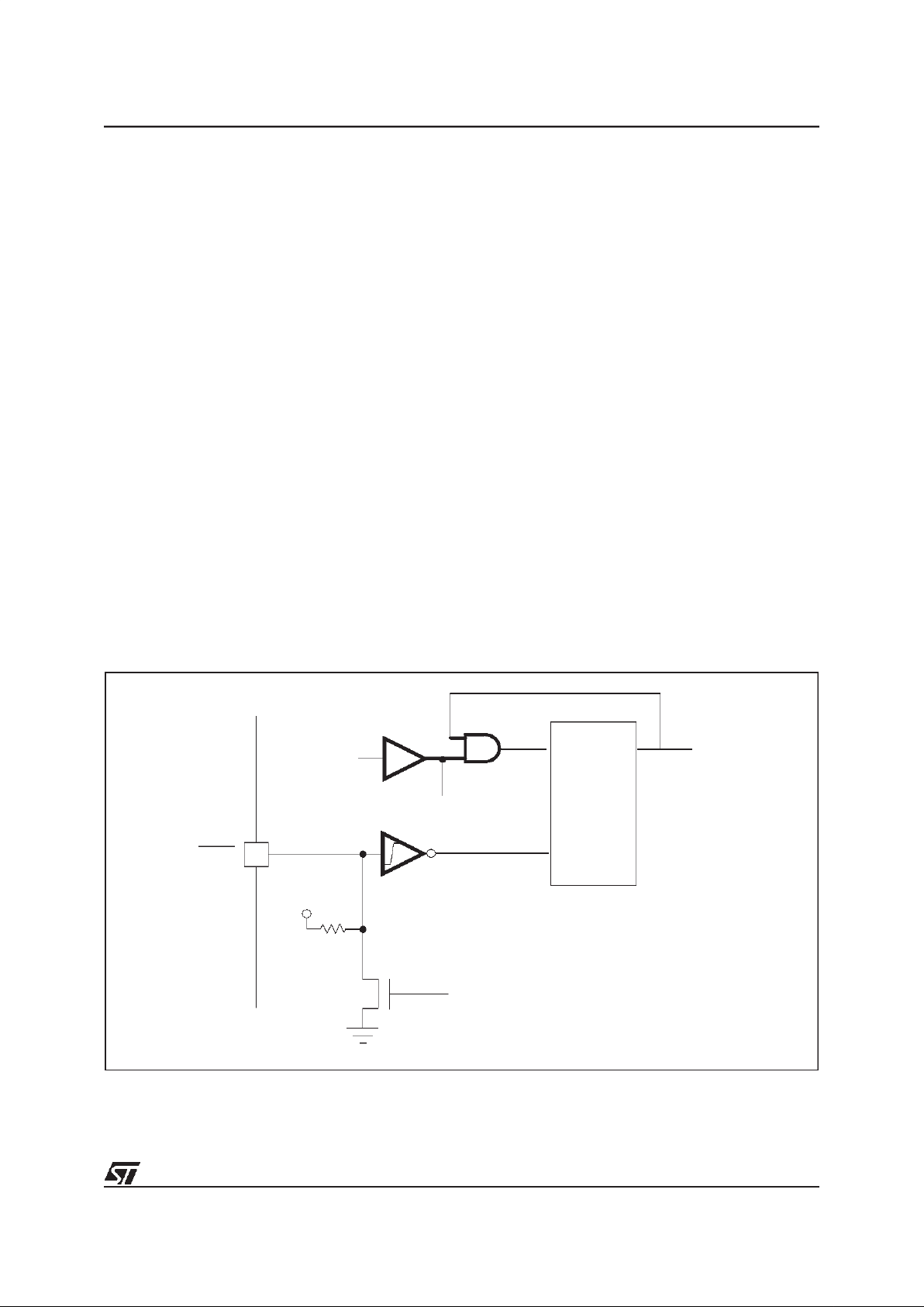
4.1.1 Introduction
Each I/O Port can contain up to 8 individually programmable I/Os. The MCU features seven 8-bit
Ports (A, B, C,... G) and one 6-bit-port (H). Each I/
O pin is dedicated to its main functionality, thus reducing and simplifying its programmability.
The current chapter describes the generic I/O
structure used in the MCU.
All I/Os are based on a generic circuit, of which a
block diagram is given inFigure 13. In most cases
the functions are simplified, and several subblocks may be missing (such as, for instance, the
analog switch on ports B to H or pull-up and interrupt logic for most of the I/O ports). Some registers
may also be absent where their functionality is redundant: it is therefore advisable to consult the
Memory Map in section1.3 and the pin description
in section 1.2 for proper use of any particular I/O.
Only ports C4, C5, D4, D5, F0,F1, F2, F3, G3 feature interrupt capability.
The following sub-section 4.1.2 contains generic
information on ST7 I/O ports. For information specific to this device, please refer to sub-section
4.1.3.
4.1.2 Generic I/O Features
The I/O ports offer the following generic features:
– inputs with Schmitt trigger
– analog inputs, when connected via internal mul-
tiplexer
– interrupt generation, maskable by software
– EMI compliance thanks to reduced noise radia-
tion due to lowered cross-current in push pull
mode and reduced input susceptibility. This fea-
ture is particularly relevant in RDS applications.
Each
generic
I/O pin may be individually program-
mable by software as:
– input: no pull-up, no interrupt generation
– input: pull-up, no interrupt generation
– input: pull-up, interrupt generation
– input: pull-down, no interrupt generation
– output: push-pull
– output: open-drain, no pull-up
– output: open-drain, with pull-up
4.1.2.1 Port Registers
Each port may be associated with up to four registers:
–
DATA REGISTER
(DR)
Address 0000 0000 000x xx00b; always present.
–
DATA DIRECTION REGISTER
(DDR)
Address 0000 0000 000x xx01b; always present.
–
OPTION REGISTER
(OR)
Address 0000 0000 000x xx10b; depending on
I/O dedication.
– PULL-UP REGISTER(PUR)
Address 0000 0000 000x xx11b; depending on
I/O dedication.
These are not internal CPU registers and must be
accessed by reading and writing to the relevant
memory locations. Refer toTable 1- Memory Map
for the respective addresses and reset values.
4.1.2.2 Functional Description
Each I/O pin may be programmed independently
as an analog input if the port features analog capabilities, as a digital input or a digital output with various variants, using the corresponding register
bits. When programmed as a digital input, a pull-up
or a pull-down resistor can, if present, be activated
by software. Only when enabling the pull-up, can
an interrupt function be programmed by software.
When programmed as an output, the I/O pin can
be programmed to operate either in push-pull or in
open-drain mode.
The interrupts generated by a port (active low) are
“ORed” to a single interrupt line that can be routed
to a CPU interrupt.
Page 25
25/117
ST7285C
I/O PORTS (Cont’d)
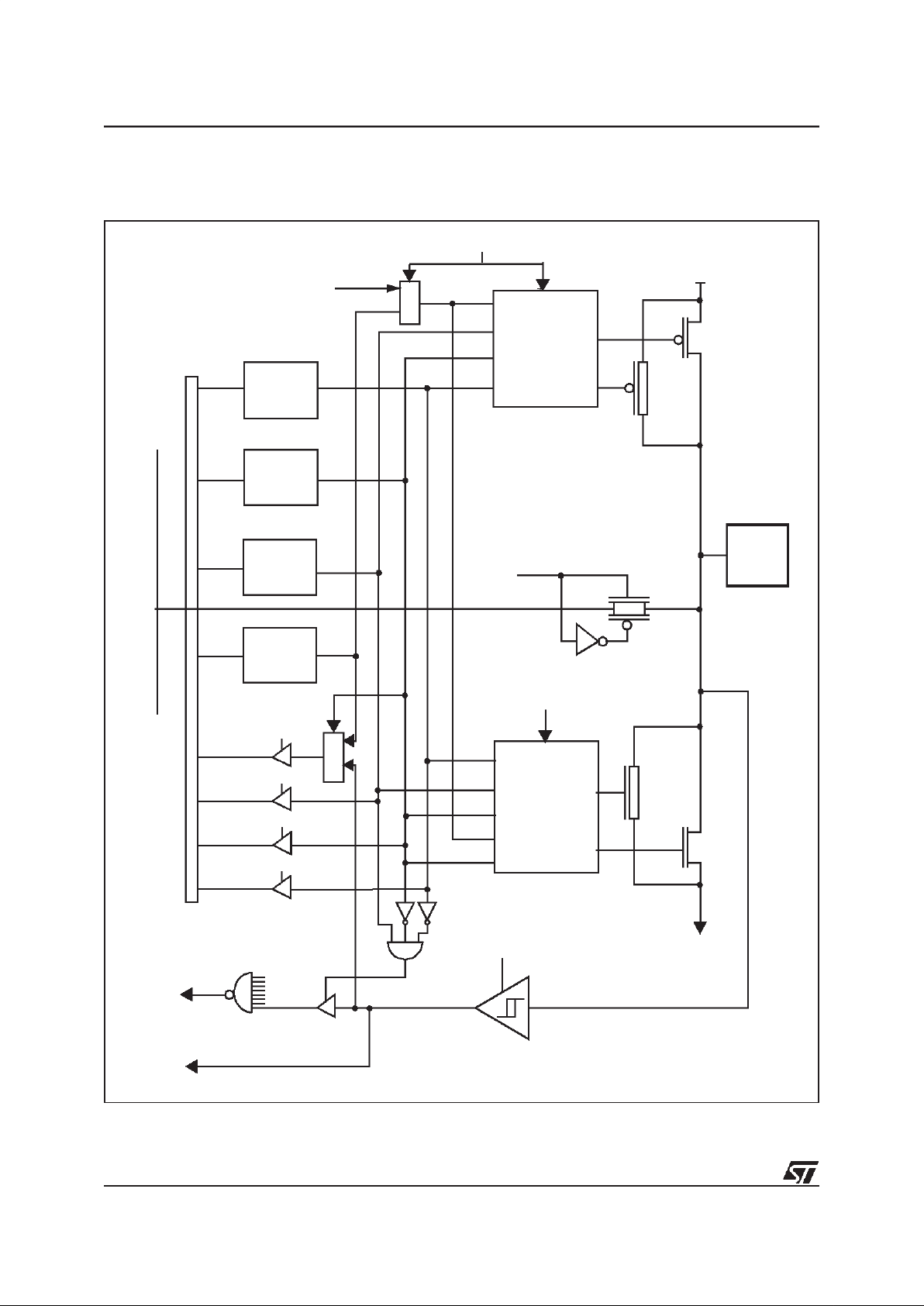
Figure 13. Generic I/O Circuitry
V
DD
PAD
FROM
OTHER
BITS
DR SEL
OR SEL
DDR SEL
PUR SEL
PUR
DDR
OR
DR
DAT A BUS
INTERRUPT
M
U
X
SIGNAL FROM ALTERNATE
TRIGGER ENABLE
PAD_TRIG
ANALOG
SWITCH
ANALOG ENABLE
COMMON ANALOG RAIL
from
ADC
M
U
X
ALTERNATE FUNCTION ENABLE
CONFIGURATION
DECODER
ALTERNATE FUNCTION ENABLE
CONFIGURATION
DECODER
FUNCTION
Page 26
26/117
ST7285C
I/O PORTS (Cont’d)
4.1.2.3 Operating Modes
All I/O pins may be configured as inputs or outputs
by programming the corresponding bits of the DR,
DDR, OR and PUR memory-mapped registers.
Table 6 illustrates the available operating modes.
During Reset, DR, DDR, OR and PUR are initialized to a Low level.
Table 6. I/O Operating Modes
Note:
(1) This state can add static current consumption.
– Input Mode
In input mode, both the analog multiplexer and the
port buffer are switchedto a high impedance state.
To avoid ringing with slowly rising or falling input
signals and to increase noise immunity, the inputs
are equipped with Schmitt-triggers.
The state of the pin is readable through the Data
Register. The pin state is read directly from the
Schmitt Trigger’s output and not from the Data
Register.
There are four different input modes, as illustrated
in Table 6.
Note: Pull-up and pull-down devices are not implemented by means of linear resistors, but by means
of resistive transistors.
– Interrupt function
The interrupt signals of all activated bits are
NANDed together, so that whenever at least one
of the activated inputs goes low, the port’s common interrupt output will go high in order to activate the CPU interrupt input.
– Output Mode
In output mode, the port output buffer is activated
and drives the output according to the content of
the data register, DR. In this mode, the analog
multiplexer, when present, is switched to high impedance and the interrupt is disabled.
Data written to the DR is directly copied to the output pins. A read operation of DR will be directly
performed from the DR register, so that the output
data stored in DR is readable, regardless of the
logic levels at the output pin due to output loading.
There are three different output modes for the
standard I/O pins as illustrated inTable 6.
– Alternate function
Alternate functions take priority over standard I/O
programming; if a peripheral needs to use a pad,
the alternate function is automatically activated.
The signal from the peripheral is output to the pad
(automatically configured in this case in push-pull
or open drain modes without pull-up and pulldown), and controlled directly by the peripheral.
The signal to be input to the peripheral from the
pad is taken after the schmitt trigger and is controlled directly by the peripheral. In this case, the pin’s
state is readable as in Input Mode by addressing
the Data Register and by configuring the PAD in
Input Mode (DDR=0).
– Analog Input Mode
In analog input mode (activated by the ADC), the
analog multiplexer is activated and switches the
analog voltage present on the selected pin (pins
PA0 to PA7) to the common analog rail. The common analog rail is connected to the Analog to Digital converter (see Section4.6) input. It is not recommended to change the voltage level or loading
on any port pin while conversion is in progress.
Furthermore it is not recommended to have clocking pins located close to a selected analog pad.
WARNING: Before activating the Analog Input
Mode, the I/O state must be set to:
INPUT, NO PULL-UP, NO INTERRUPT
(DDR = 0, OR = 0, PUR = 1)
The alternate function must not be activated as
long as the pad is configured as Input with Interrupt, in order to avoid generating spurious interrupts.
Analog input mode is only implemented for pins
PA0 to PA7. The analog input voltage level must
be within the limits stated in the Absolute Maximum Ratings.
DDR OR PUR Mode Option
0 0 0 input pull-up, no interrupt
0 0 1 input no pull-up, no interrupt
0 1 0 input pull-up, interrupt
0 1 1 input pull-down, no interrupt
1 0 0 output open-drain, pull-up
1 0 1 output open-drain, no pull-up
1 1 0 output RESERVED
(1)
1 1 1 output
push-pull, nopull-up, no
pull-down
Page 27
27/117
ST7285C
I/O PORTS (Cont’d)
4.1.3 I/O Port Implementation
On the ST7285C, the pull down is always absent,
the pull up exists only where an interrupt facility is
present (Ports C4, C5, D4, D5, F0, F1, F2, F3,
G3). On port A, the analog inputs are directly controlled by the ADC.The I/O port register configurations are reduced to the following.
4.1.3.1 Ports A0-A7, B0-B7, C0-C3, C6, C7, D0D3, D6, D7,E0-E7, F4-F7, G0-G2, G4-G7, H0-H5
These ports do not offer interrupt capabilities.
Note: Open drain I/O is implemented on I2C pins
(pins 19 and 20) and high voltage pins (PH3/4/5).
The design uses special I/O devices without P
channel, thus forbidding the push pull configuration.
In this case there is neither pull up register nor option register. These registers do not exist and so
cannot be read or written to.
4.1.3.2 Ports C4, C5, D4, D5, F0-F3, G3
These ports offer interrupt capabilities.
In this case there is no pull up register since the
pull-up is present only when the interrupt feature is
selected. This register does not exist and so cannot be read or written to.
Switching these I/O ports from one state to another should be done in such a sequence as to prevent unwanted side effects. Recommended safe
transitions are illustrated inFigure 14. Other transitions are potentially risky and should be avoided,
since they are likely to present unwanted side-effects such as spurious interrupt generation.
Figure 14. Recommended I/O State Transition Diagram
DDR MODE OPTION
0 input no pull-up, no pull-down, no interrupt
1 output push-pull (or open drain: see note)
DDR OR
MOD
E
OPTION
0 0 input
no pull-up, no pull-down,
no interrupt
0 1 input interrupt, pull-up
1 0 output open-drain, no pull-up
1 1 output
push-pull, no pull-up,
no pull-down
110001
Interrupt
pull-up
push-pull
no pull-up
open-drain
no pull-up
no pull-down
INPUT
OUTPUT
OUTPUT
10
no pull-up
no interrupt
INPUT
no pull-down
(Reset state)
XX
= DDR, OR
Page 28

28/117
ST7285C
4.2 SERIAL COMMUNICATIONS INTERFACE
4.2.1 Introduction
The Serial Communications Interface (SCI) offers
a flexible means of full-duplex data exchange with
external equipment requiring an industry standard
NRZ asynchronous serial data format. The SCI offers a very wide range of Baud rates thanks to the
presence of two Baud rate generator systems: the
first is of conventional type and yields common
communications Baud rates with standard oscillator frequencies; the second features a programmable prescaler capable of dividing the input frequency by any factor from 1 to 255, thus offering a
very wide range of Baud rates even with nonstandard oscillator frequencies. Transmitter and
Receiver circuits are independent and can operate
at different Baud rates; indeed, each can select either type of Baud rate generator. External connections are by means of two I/O pins: TDO (Port
PB0) for the Transmit Data output and RDI (Port
PB1) for the Receive Data input.
4.2.2 Features
– Full duplex, asynchronous communications
– NRZ standard format (Mark/Space)
– Dual Baud rate generator systems
– Independently programmable transmission and
reception Baud rates
– Separate Transmit and Receive Baud rates
– Programmable word length (8 or 9 bits)
– Receive buffer full, Transmit buffer empty and
End of Transmission flags
– Receiver wake-up function by the most signifi-
cant bit or by idle line
– Muting function for multiprocessor configurations
–Separate enable bitsforTransmitter andReceiver
– Noise, Overrun and Frame Error detection
– Four interrupt sources with flags
– Overall accuracy better than 1% of Baud rate.
4.2.3 Serial Data Format
Serial data is transmitted and received as frames
comprising the following elements:
– An Idle Line in the ”high” state prior to transmis-
sion or reception.
– A Start bit inthe ”low” state, denoting the start of
each character.
– Character dataword (8 or 9 bits), least significant
bit first.
– A Stop bit in the ”high” state, indicating that the
frame is complete.
Word length may be selected as being either 8 or 9
bits by programming the M bit in the SCCR1 control register.
An Idle Line condition is interpreted on receiving
an entire frame of ”ones”.
A Break is interpreted on receiving ”zeros” for
some multiple of the frame period.
4.2.4 Data Reception and Transmission
The following description is best read with reference to the SCI Block Diagram illustrated in Figure
1, where it will be noted that the SCDR data register is shown as two separate registers, one for
transmitted data and the other for received data.
The Serial Communications Data Register (SCDR)
performs a dual function (Read And Write),since it
accesses two separate registers, one for transmission (TDR) and one for reception (RDR). The TDR
register provides the data interface between the internal bus and the output shiftregister for data to be
transmitted, while the RDR register provides an interface between the input shift register and the internal bus for incoming data.
When the SCDR is read, the RDR is accessed and
its contents are transferred to the data bus. The
RDRF (RDR Full Flag) in the SCSR register is set
to ”1” as soon as the word in the receiver shift register is transferred to the RDR register.
When the SCDR is written to, the data word is
transferred to the TDR register. The TDRE flag
(TDR empty) in the SCSR register is set to ”1” as
soon as the word in the TDR is transferred to the
transmit shift register.
Incoming data is received in a serial shift register
and then transferred to a parallel Receive Data
Register (RDR) as a complete word, thus allowing
the next incoming character to be received in the
shift register while the current character is still in
the RDR.
Oversampling techniques are used for data recovery by discriminating between valid incoming data
and noise.
4.2.5 Receiver Muting and Wake-up Feature
In multiprocessor configurations it is often desirable that only the intended message recipient
should actively receive the full message contents,
thus reducing redundant SCI service overheads
for all non addressed receivers. Communications
protocols in such configurations generally issue
the recipient address as a message header.
Page 29

29/117
ST7285C
SERIAL COMMUNICATIONS INTERFACE(Cont’d)
Each receiving device decodes this address header under program control and all non addressed
receivers may be placed in a sleep mode by
means of the Muting function, thus avoiding the
message contents from generating unnecessary
requests for service. This is achieved by inhibiting
all reception flags and interrupt generation when
Muting is enabled. A muted receiver may be reawakened in one of two ways: by Idle Line detection or by Address Mark detection. The wake-up
method may be programmed by programming the
WAKE bit in the SCCR1 register.
Receiver wake-up by Idle Line detection takes
place as soon as the Receive line is recognised as
being idle. An Idle Line condition is detected upon
receiving 10 or 11 consecutive ”ones”, depending
on whether a word has been defined as comprising 8 or 9 data bits. This wake-up method is selected by programming the WAKE bit to ”0”.
Receiver wake-up by Address Mark detection
takes place on receiving a ”1” as the most significant bit of a word, thus indicating that the message
is an address. This wake-up method is selected by
programming the WAKE bit to ”1”.
4.2.6 Baud Rate Generation
The following description is best read with reference to the SCI Baud Rate and External Prescaler
Diagram illustrated in Figure 2.
The CPU Clock is first divided by 16 by the first divisor block, then again divided by the division factor selected for the first prescaler, indicated by PR.
This division factor can be selected to be 1, 3, 4 or
13, depending on the setting of the SCP0 and
SCP1 bits (bits 6 and 7) in the SCBRR register (refer to the register description). The output from the
first prescaler will thus be the CPU Clock frequency divided by 16, 48, 64 or 208. This master clock
is available both to the conventional Baud Rate
Generator and to the External Prescaler.
The conventional Baud Rate Generator is enabled
by setting the relevant section (RX or TX) of the
External Prescaler to 00h. In this case the master
clock frequency is further divided by 1, 2, 4, 8, 16,
32, 64 or 128, depending on the settings of bits
SCT0, SCT1 and SCT2 in the case of the transmitter, and SCR0, SCR1 and SCR2 in the case of the
receiver (refer to the SCBRR register description).
If the External Prescaler Receive or Transmit
Baud Rate Register, PSBRT or PSBRR is set to a
value other than zero, that section of the prescaler
will be operational in place of the conventional
Baud Rate Generator. The output clock rate sent
to the transmitter or to the receiver will be the output from the first prescaler divided by a factor
ranging from 1 to 255 set in the External Prescaler
Receive or Transmit Baud Rate Register. As can
be seen the External Prescaler option gives a very
fine degree of control on the Baud rate, whereas
the conventional Baud Rate Generator retains industry standard software compatibility.
4.2.7 SCI Register Overview
The registers described in the following paragraphs allow full control of the various features
and parameters of the Serial Communications Interface. Refer also to the Memory Map.
4.2.7.1 Data Register (SCDR)
Address: 0051h — Read/Write
Reset Value: XXh
Contains the Received or Transmitted data char-
acter, depending on whether it is read or written to.
4.2.7.2 Control Register 1 (SCCR1)
Address: 0053h — Read/Write
Reset Value: XXh
Contains bits to select the desired word length and
the wake-up mode.
Bit-7 = R8
Receive Data Bit 8
If bit M is set at one, R8 will be used to store the
9th bit on reception.
Bit-6 = T8
Transmit Data Bit 8
Used to store the 9th data bit of the transmitted
word, when 9-bit word length is selected (bit M set
to ”1”).
Bit-4 = M
Word Length
Determines the word length:
0 = 1 Start bit, 8 Data bits, 1 Stop bit
1 = 1 Start bit, 9 Data bits, 1 Stop bit
Bit-3 = WAKE
Wake-Up Method
1 = Address Mark
0 = Idle Line
76543210
R8 T8 - M WAKE - - -
Page 30
30/117
ST7285C
SERIAL COMMUNICATIONS INTERFACE(Cont’d)
4.2.7.3 Control Register 2 (SCCR2)
Address: 0054h — Read/Write
Reset Value: 00h
Contains four control bits which allow interrupts
generated by TDR Empty, Transmit Complete,
RDR Full and Idle Line to be enabled or disabled.
Also contains four control bits to enable or disable
Transmission, Reception, Receiver Wake-Up and
Send Break.
Bit-7 =
TIE
Transmitter Interrupt Enable
Authorizes an interrupt when set at one and when
the TDRE (transmission register empty) flag is set
to “1” indicating that the last word has been transmitted. When TIE is at zero this interrupt is disabled.
Bit-6 = TCIE
Transmission Complete Interrupt En-
able
This bit setto “1” enables an interrupt when theTC
flag (transmission competed) changes to “1”.
When TCIE is at “0” this interrupt is disabled.
Bit-5 = RIE
Receiver Interrupt Enable
Authorizes an interrupt when set to “1” and when
either the RDRF (Receive Data Register Full) flag
or the OR (Overspeed on Reception) flag is set to
“1”, indicating that the last word has been transmitted. When TIE is set to “0”, this interrupt is disabled.
Bit-4 = ILIE
Idle Line Interrupt Enable
This bit at “1” enables an interrupt if the IDLE flag
changes to “1” (which corresponds to an idle line
on reception). The interrupt cannot occur if the
IDLE bit is at “0”.
Bit-3 =
TE
Transmitter Enable
This bit at “1” enables the transmitter. At start-up,
the transmitter sends a preamble (ten or eleven
ones). During transmission, a “0” pulse on the TE
bit (“0” followed by “1”) sends a preamble after the
current word. Setting the TE bit to “0” switches the
output line to a high impedance state at the end of
the word currently being transmitted.
Bit-2 = RE
Receiver Enable
The RE bit at “1” enables the receiver which begins searching for a START bit. The RE bit at “0”
disables the receiver and resets the associated
status bits to “0” (RDRF, IDLE, OR, NF and FE).
Bit-1 = RWU
Receiver Wake-Up
The RWU bit at “1” mutes the receiver. The wakeup mode is determined by the WAKE bit (bit 3 in
SCCR1). As long as RWU remains at “1”, the flags
relating to the receiver cannot rise to “1”.
Writing “0” to RWU forces an exit from the muted
state.
As soon as the wake-up sequence is recognized,
the RWU bit is forced to “0”. If the wake-up selected mode corresponds to the reception of a preamble, the RWU bit cannot be set to “1” as long as the
reception remains idle. If the selected wake-up
mode corresponds to the reception of a “1” on the
most significant bit, the reception of this particular
word wakes up the receiver and sets the RDRF
flag to “1”, which allows the receiver to receive this
word normally and to use it as an address word.
Bit-0 = SBK
Send Break
This bit set to “1” tells the transmitter to send a
whole number of BREAKS (all bits at “0” including
the stop bit). At the end of the last BREAK the
transmitter inserts an extra “1” bit in order to acknowledge the START bit. If the SBK bit is set to
“1” and then to “0”, the transmitter will send a
BREAK word at the end of the current word.
4.2.7.4 Status Register (SCSR)
Address: 0050h — Read Only
Reset Value: 1100 0000b
Contains four flags which denote conditions which
can lead to interrupts if the corresponding bits of
SCCR2 are set: TDR Empty, Transmit Complete,
RDR Full and Idle Line. These flags are used for
management of the SCI interrupt system.
Also contains three flags which indicate error conditions due to Overrun, Noise and Framing.
Bit-7 =TDRE
Transmit Data Register Empty
Indicates that the content of the transmission data
register has been transferred into the shift register.
If the TDRE bit is at “0”, it indicates that the transmission has not yet occurred and that a write operation into the data register would overwrite previous data. The TDRE bit is reset to “0” by an SCSR
access followed by a write operation into the transmission data register. Data will not be transferred
to the shift register as long as the TDRE bit is not
reset to “0”.
Bit-6 =
TC
Transmission Complete
76543210
TIE TCIE RIE ILIE TE RE RWU SBK
76543210
TDRE TC RDRF IDLE OR NF FE -
Page 31

31/117
ST7285C
SERIAL COMMUNICATIONS INTERFACE(Cont’d)
The TC bit is automatically set to “1” when transmission of a frame containing Data, a Preamble or
a Break is complete, if:
– TE = ”1”, TDRE = ”1”, no word is currently being
transmitted and no preamble or BREAK is await-
ing transmission.
– TE = ”0” and the current word or preamble or
BREAK has been transmitted
The TC bit is aflag indicating that one of the above
sequences has occurred. This bit is reset to “0” by
an access to the SCSR followed by a write operation into the data register or when TDRE is reset to
“0”. Transmitter operation is in no way modified by
the status of this bit.
Bit-5 =
RDRF
Received Data Ready Flag
This bit, when set to “1”, indicates that the content
of the RDR has been transferred into the SCDR. If
a Frame Error or Noise has been detected during
reception, the corresponding flags will be set.
The RDRF bit is reset to “0” by an access to the
SCSR followed by a data register read operation.
Bit-4 = IDLE
Idle Line Detect
When the idle line detect bit is set it indicates that
the receiver idle line is detected (receipt of a minimum number of ones (10 when M=0, 11 when
M=1) to constitute the number of bits in the frame
format. This allows a receiver that is not in the
wake-up mode to detect the end of a message or
the preamble of a new message or to re-synchronize with the transmitter. The IDLE bitis cleared by
accessing the SCSR (with idle set) followed by a
read of the data register. The IDLE bit will not be
set again until the RDRF bithas been set itself (i.e.
a new idle line occurs). The IDLE bit is not set by
an idle line when the receiver wakes up from wake
up mode.
Bit-3 =
OR
Overrun Error
This bit is set to “1”, when the word currently being
received in the shift register is ready to be transferred into the data register while the latter is already full (RDRF=”1”). All transfers will remain disabled as long as RDRF remains at “1”. Data register content will not be lost but the shift register will
be overwritten. The OR bit is reset by an access to
the SCSR followed by a data register read operation.
Bit-2 = NF
Noise Flag
This bit is set to “1” when noise is detected on an
acknowledge START bit or a data bit or a stop bit.
The NF is set to “1” when the noise is detected at
the rising edge of RDRF and is representative of
the word present in the data register. This bit does
not generate interrupts as it appears at the same
time as RDRF which itself generates an interrupt.
The NF bit is set to “0” by a SCSR read operation
followed by a data register read operation.
Bit-1 =
FE
Framing Error
This bit is set to “1” when the STOP bit is not recognized on reception at the expected moment, following either a de-synchronization, excessive
noise or when a BREAk is received. The word will,
however still be transferred to the data register. As
in the case of the NF bit, the FEW bit does not generate an interrupt as it appears at the same time as
RDRF bit. If the word currently being transferred
causes both frame error and reception overspeed,
it will be transferred and only the OR bit will be set
to “1”. The FE bit is reset to “0” by a SCSR read
operation followed by a data register read operation.
Bit-0 =
Unused
4.2.7.5 Baud Rate Register (SCBRR)
Address: 0052h — Read/Write
Reset Value: 00X----Xb
Contains two bits for selection of the first prescaler
factor, three bits for selection of the transmitter
rate divisor and three bits for the receiver rate divisor.
Bit-7 =SCP1
First prescaler MSB
Bit-6 =SCP0
First prescaler LSB
These 2 prescaling bits allow several standard
clock division ranges:
Bit-5 =SCT2
Transmitter rate divisor MSB
Bit-4 =SCT1
Transmitter rate divisor NSB
Bit-3 =
SCT0
Transmitter rate divisor LSB
These 3 bits, in conjunction with the 2 previous bits
define the total division applied to the bus clock to
yield the transmit rate clock in conventional Baud
Rate Generator mode.
76543210
SCP1 SCP0 SCT2 SCT1 SCT0 SCR2 SCR1 SCR0
SCP1 SCP0 PR Prescaling factor
00 1
01 3
10 4
11 13
Page 32

32/117
ST7285C
SERIAL COMMUNICATIONS INTERFACE(Cont’d)
This TR factor is used only when the PSBRT fine
tuning factor is equal to 0; otherwise, TR is replaced by the PSBRT dividing factor.
Bit-2 = SCR2
Receiver rate divisor MSB
Bit-1 = SCR1
Receiver rate divisor NSB
Bit-0 =
SCR0
Receiver rate divisor LSB
These 3 bits, in conjunction with the 2previous bits
define the total division applied to the bus clock to
yield the receive rate clock in conventional Baud
Rate Generator mode..
This RR factor is used only when the PSBRR fine
tuning factor is equal to 0; otherwise, RR is replaced by the PSBRR dividing factor.
4.2.7.6 External Receive Prescaler Division
Register (PSCBRR)
Address: 0055h — Read/Write
Reset Value: 00h
Allows setting of the External Prescaler rate divi-
sion factor for the receive circuit.
When the register is set to 00h, the conventional
Baud Rate Generator is used for the receive circuit, otherwise the master clock frequency is divided by the binary factor set in the PSCBRR register
(in the range 1 to 255).
4.2.7.7 External Transmit Prescaler Division
Register (PSCBRT)
Address: 0057h — Read/Write
Reset Value: 00h
Allows setting of the External Prescaler rate divi-
sion factor for the transmit circuit.
When the register is set to 00h, the conventional
Baud Rate Generator is used for the transmit circuit, otherwise the master clock frequency is divided by the binary factor set in the PSCBRTregister
(in the range 1 to 255).
SCT2 SCT1 SCT0 TR dividing factor
000 1
001 2
010 4
011 8
100 16
101 32
110 64
1 1 1 128
SCR2 SCR1 SCR0 RR dividing factor
000 1
001 2
010 4
011 8
100 16
101 32
110 64
1 1 1 128
76543210
PRBR7PRBR6PRBR5PRBR4PRBR3PRBR2PRBR1PRBR
0
76543210
PTBR7PTBR6PTBR5PTBR4PTBR3PTBR2PTBR1PTBR
0
Page 33

33/117
ST7285C
SERIAL COMMUNICATIONS INTERFACE(Cont’d)
Figure 15. SCI Block Diagram
FLAG
CONTROL
RECEIVE
DATA
REGISTER
RECEIVE
DATA
SHIFT
REGISTER
WAKE
UP
UNIT
RECEIVER
CONTROL
TRANSMIT
DATA
SHIFT
REGISTER
TRANSMIT
REGISTER
DATA
TDO
SCCR2
RWU
SBK
RE
TE
ILIE
RIE
TCIE
TIE
TDRETCRDRFIDLEORNFFE
1
23
46705
1
2
3
4
5
6
7
SCSR
TRANSMIT
CONTROL
R8T8
M
SCCR1
0
1
2
3
4
5
6
7
RDI
INTERNAL B US
SCI INTERRUPT
WAKE
TRANSMIT CLOCK
RECEIVE CLOCK
Page 34

34/117
ST7285C
SERIAL COMMUNICATIONS INTERFACE(Cont’d)
Figure 16. SCI Baud Rate and External Prescaler Block Diagram
RECEIVER RATE CONTROL
TRANSMITTER RATE CONTROL
TRANSMITTER
RECEIVER
PSCBRT
7
0
SCBRR
7
0
PSCBRR
7
0
EXTERNAL PRESCALER RECEIVER RATE CONTROL
EXTERNAL PRESCALER TRANSMITTER RATE CONTROL
EXTERNAL PRESCALER
CPU CLOCK
Divide by16Divide by
PR
CONVENTIONAL BAUD RATE
GENERATOR
CLOCK
CLOCK
Page 35

35/117
ST7285C
4.3 16-BIT TIMER
4.3.1 Introduction
One or more Timers may be present in the MCU,
depending on product specification. Please refer
to the Block Diagram to ascertain available product resources, and to the Memory Map for register
addresses.
Each timer consists of a 16-bit free-running counter driven by a programmable prescaler, as well as
the control logic required to implement two input
capture and two output compare registers. The
timer may be used for a variety of purposes,
amongst which pulse length measurement of up to
two input signals and generation of up to two output waveforms (e.g. PWM). The Timer Block Diagram is illustrated in Figure 1.
Pulse lengths and waveform periods can vary from
a few microseconds to many seconds, thanks to
the programmable prescaler. When running with a
4MHz internal CPU clock, the timer can have a
resolution of 0.5, 1 or 2µs, depending on the setting of the clock control bits in the Timer Control
Register (TCR2). A software selectable external
clock input pin is available.
Since the timer has a 16-bit architecture, each of
its specific functional blocks is associated with a
register pair. These registers contain the high order byte and the low order byte respectively of the
related function. Access to the high order byte inhibits the associated timer function until the low order byte is also accessed.
Correct software procedures should set bit ‘I’ of
the Condition Code Register before accessing the
high order byte to prevent an interrupt from occurring between accesses to the high and low order
bytes of any register.
In normal operating mode, reading the MSB of the
Input Capture register inhibits Input Capture until
the LSB is read. This mechanism allows Input capture to be disabled when the pin is connected to an
I/O bit.
When the Pulse Width Modulation (PWM) and
One Pulse Mode (OPM) features are selected together, the PWM mode is the only active one.
4.3.2 Counter
The key element of the Programmable Timer is a
16-bit free running counter and its associated register. The counter is preceeded by a prescaler
which divides the internal clock by two, four or
eight, depending on the setting of the clock control
bits of the Timer Control Register (TCR2), as illustrated in Table 1 below.
Table 7. Clock Control Bits
Software can read the counter at any time without
affecting its value, either from the Counter Registers or from the Alternate Counter Registers. The
only difference between these two read-only register pairs is the way the overflow flag (TOF) is handled during a read sequence.
A read sequence where only the least significant
byte of the free running counter is read (from either
the Counter Register or the Alternate Counter
Register), will receive the LSB of the count value
at the time of the read.
A read of the most significant byte (from either the
Counter Register or the Alternate Counter Register) simultaneously returns the MSB of the count
value and causes the LSB to be transferred to a
buffer. The buffered value remains unchanged until the 16-bit read sequence is completed, even if
the user reads the MSB several times. The read
sequence is completed by reading the LSB, which
actually returns the buffered value.
As shown in Figure 2, Figure 3 and Figure 4, the
free-running counter is set to FFFCh on Reset.
During a Power-On Reset (POR) cycle, the counter is loaded with FFFCh and begins running.
CC1 CC0 Clock Divisor
00 4
01 2
10 8
1 1 External Clock
Page 36

36/117
ST7285C
16-BIT TIMER(Cont’d)
Figure 17. Timer Block Diagram
MCU-PERIPHERAL INTERFACE
COUNTER
ALTERNATE
REGISTER
OUTPUT
COMPARE
REGISTER
OUTPUT COMPARE
EDGE DETECT
OVERFLOW
DETECT
CIRCUIT
1/2
1/4
1/8
8-bit
buffer
ST7 INTERNAL BUS
LATCH1
OCP1
ICP1
TCLK
CPU CLOCK
TIMER INTERRUPT
ICF2ICF1 000OCF2OCF1 TOF
PWMOC1E
EXEDG
IEDG2CC0CC1
OC2E
OPMFOLV2ICIE OLVL1IEDG1OLVL2FOLV1OCIE TOIE
ICP2
LATCH2
OCP2
8
8
8low
16
8 high
16 16
16
16
CC1 CC0
TCR1
TCR2
TSR
6
16
888
888
high
low
high
high
high
low
low
low
EXEDG
EXEDG
PORT
TIMER INTERNAL BUS
CIRCUIT1
EDGE DETECT
CIRCUIT2
CIRCUIT
1
OUTPUT
COMPARE
REGISTER
2
INPUT
CAPTURE
REGISTER
1
INPUT
CAPTURE
REGISTER
2
CC1 CC0
16 BIT
FREE RUNNING
COUNTER
Page 37

37/117
ST7285C
16-BIT TIMER(Cont’d)
When the counter rolls over from FFFFh to 0000h,
the Timer Overflow flag (TOF) of the Timer Status
Register (TSR) is set. A timer interrupt is then generated if the TOIE enable bit of the Timer Control
Register (TCR1) is set, provided the I bit of the
CCR is cleared. If one of these conditions is false,
the interrupt remains pending to be issued as soon
as they are both true. The interrupt request is
cleared by reading TSR while TOF is set, followed
by an access (read or write) to the LSB of the
Counter Register.
The TOF flag is not affected by accesses to the Alternate Counter Register. This feature allows simultaneous use of the overflow function and reads
of the free running counter at random times (for
example, to measure elapsed time) without risking
to clear the TOF flag erroneously. Accesses to the
timer without the intention of servicing the TOF
flag should therefore be performed to the Alternate
Counter Register while only the TOF service routine accesses the Counter Register.
The free running counter can be reset under software control, by writing to the LSB of the Counter
Register or of the Alternate Counter Register. The
counter and the prescaler are then configured to
their reset conditions. This reset also completes
any 16-bit access sequence. All flags and enable
bits are unchanged.
The value in the counter registers repeats every
131,072, 262,144, or 524,288 internal processor
clock cycles,depending on the clock control option
selected in TCR2. As shown in the timing diagrams, the counter increment is triggered by a falling edge of the CPU clock.
The timer is not affected by WAIT mode. In HALT
mode, the counter stops counting until the mode is
exited. Counting then resumes from the previous
count (MCU awakened by an interrupt) or from the
reset count (MCU awakened by a Reset).
4.3.3 External Clock
When the external clock is selected by setting the
relevant clock control bits in TCR2, the counter
clocks on each external clock rising edge, if
EXEDG in TCR2 is set, or the falling edges if reset,
and is synchronised with the falling edge of the internal CPU clock.
At least four falling edges of the CPU clock must
occur between two consecutive active edges of
the external clock; thus the external clock frequency must be less than a quarter of the CPU clock
frequency.
The parasitic pulses generated by the EXTEDG
and EXTCLKE transitions are filtered during two
clock periods, so the manipulation of the external
clock control bits must occur before or after two internal clock periods.
Page 38

38/117
ST7285C
16-BIT TIMER(Cont’d)
Figure 18. Timer Timing Diagram, internal clock divided by 2
Figure 19. Timer Timing Diagram, internal clock divided by 4
Figure 20. Timer Timing Diagram, internal clock divided by 8
CPU CLOCK
FFFD FFFE FFFF 0000 0001 0002 0003
INTERNAL RESET
INTERNAL TIMER CLOCK T10
COUNTER REGISTER
OVERFLOW FLAG TOF
FFFC FFFD 0000 0001
CPU CLOCK
INTERNAL RESET
INTERNAL TIMER CLOCK T10
COUNTER REGISTER
OVERFLOW FLAGTOF
INTERNAL TIMER CLOCK T00
CPU CLOCK
INTERNAL RESET
INTERNAL TIMERCLOCK T10
COUNTER REGISTER
OVERFLOW FLAG TOF
FFFC FFFD
0000
INTERNAL TIMERCLOCK T00
Page 39

39/117
ST7285C
16-BIT TIMER(Cont’d)
4.3.4 Input Capture
The timer features two input capture registers and
an input capture interrupt enable bit.
The Input Capture Registers (ICR1 and ICR2)
each consist of two 8-bit registers: the most significant byte registers (ICHR1 and ICHR2), and the
least significant byte registers (ICLR1 and ICLR2).
In the following description, the variableimay represent 1 or 2.
ICRiis a read-only registers used to latch the value of the free running counter after a defined transition is sensed by the input capture edge detector
at pin ICAPi. This transition is software programmable through the IEDGibit of the Timer Control
Register (TCRi). When IEDGiis set, a rising edge
triggers the capture; when IEDGiis low, the capture is triggered by a falling edge.
When an input capture occurs, the ICFiflag in the
Timer Status Register (TSR) is set. An interrupt is
requested if the interrupt enable bit, ICIE, of TCR1
is set, provided the I bit of the CCR is reset. Otherwise, the interrupt remains pending until both conditions become true. It is cleared by reading the
TSR followed by a read or write of the LSB of ICRi.
The result stored in ICRiis one more than the value of the free running counter on the rising edge of
the internal processor clock preceding the active
transition on the ICAPipin (see Figure 5). This delay is required for internal synchronization. Therefore, the timing resolution of the input capture system is one count of the free running counter, i.e. 2,
4 or 8 internal clock cycles, depending on the clock
control bits of TCR2.
The free running counter is transferred to ICRion
each proper signal transition regardless of whether the Input Capture Flag ICFiis set or cleared.
The ICRialways contains the free running counter
value which corresponds to the most recent input
capture.
After reading the MSB of ICRi, transfer of input
capture data is inhibited until the LSB is also read.
This implies that the minimum pulse period is determined by the time required to respond to the interrupt and to execute the service routine.
Reading ICLRidoes not inhibit transfer of counter
data. The minimum pulse period is determined by
the time required to read the least significant byte
and to perform necessary actions. There is no
conflict between reading ICRiand the running
counter transfer, since they occur on opposite
clock edges as shown in Figure 5.
ICRiis undetermined on power-on, and is not affected by an external Reset. Hardware circuitry
must provide protection against generating an undesired input capture when changing the edge
sensitivity option of the ICAPipin by programming
the IEDGibit.
During HALT mode, if at least one valid input capture edge occurs on the ICAPipin, the input capture detection circuitry is armed. This does not set
any timer flags, and does not ”wake-up” the MCU.
If the MCU is awoken by an interrupt, the input
capture flag will be active, and data corresponding
to the first valid edge during HALT mode will be
present. If HALT mode is exited by a Reset, the input capture detection circuitry is reset and thus,
any active edge that occurred during HALT mode
will be lost.
Figure 21. Input Capture Timing Diagram
FF01 FF02 FF03
FF03
CPU CLOCK ÷2
CPU CLOCK ÷4
CPU CLOCK ÷8
INTERNAL CLOCK T10
INTERNAL CLOCK T11
COUNTER REGISTER
ICAPi PIN
ICAPi FLAG
ICAPi REGISTER
Page 40

40/117
ST7285C
16-BIT TIMER(Cont’d)
4.3.5 Output Compare
Two output compare registers are present: Output
Compare Register 1 and Output Compare Register 2 (OCR1 and OCR2). These registers can be
used for several purposes, such as controlling an
output waveform or indicating when a period of
time has elapsed. The OCMPipin is associated
with the Output Compareifunction (i= 1 or 2).
The Output Compare Registers are unique in that
all bits are readable and writable and are not affected by the timer hardware or by Reset. If a compare function is not used, the two bytes of the corresponding Output Compare Registers can be
used as general purpose storage locations.
4.3.5.1 Output Compare Registers
The Output Compare Registeri(OCRi) is a 16-bit
register, which is made up of two 8-bit registers:
the most significant byte register (OCHRi) and the
least significant byte register (OCLRi).
In this section, the index,i, may be 1 or 2.
The content of OCRiis compared with the content
of the free running counter once during every timer
clock cycles, i.e. once every 8, 4 or 2 internal processor clock periods or 2 external clock periods according to the clock control bits of the Timer Control Register (TCR2). If match is found, the Output
Compare Flag OCFiof the TSR is set and the Output Level bit (OLVLi) of the TCR1 is clocked to the
OCMPipin (see output compare timing diagrams
Figure 6, Figure 7, Figure 8). OLVLiis copied to
the corresponding output level latch and hence, to
the OCMPipin regardless of whether the Output
Compare Flag (OCFi) is set or not. The value in
the OCRiand the OLVLibit should be changed af-
ter each successful comparison in order to control
an output waveform or establish a new elapsed
timeout.
An interrupt accompanies a successful output
compare if the corresponding interrupt enable bit
OCIE of the TCR1 is set, provided the I-bit of the
CCR is cleared. Otherwise, the interrupt remains
pending until both conditions are true. It is cleared
by a read of TSR followed by an access to the LSB
of the OCRi.
After a processor write cycle to the OCHRiregister, the output compare function is inhibited until
the OCLRiis also written. Thus, the user must
write both bytes if the MSB is written first. A write
made to only the LSB will not inhibit the compare
function. The minimum time between two successive edges on the OCMPipin is a function of the
software program and the clock control bits of the
TCR2.
The OCMPioutput latch is forced low during reset
and stays low until valid compares change it to a
high level. Because the OCFiflag and the OCR
i
are undeterminate at power-on and are not affected by an external reset, care must be exercise
when initiating the output compare function with
software. The following procedure is recommended to prevent the OCFiflag from being set between the time it is read and the write to OCRi:
– Write to OCHRi(further compares are inhibited).
– Read the TSR (first step of the clearance of OC-
Fi, which may be already set).
– Write to OCLRi(enables the output compare
function and clears OCFi).
Page 41

41/117
ST7285C
16-BIT TIMER(Cont’d)
Figure 22. Output Compare Timing Diagram, internal clock divided by 8
Figure 23. Output Compare Timing Diagram, internal clock divided by 4
Figure 24. Output Compare Timing Diagram, internal clock divided by 2
INTERNAL CPU CLOCK
INTERNAL TIMER CLOCK T01
INTERNAL TIMER CLOCK T11
COUNTER
FFFC FFFD
FFFC
COMPARE REGISTER
COMPARE REGISTER LATCH
OUTPUT REGISTER FLAG OCFI AND OCMPI PIN
INTERNAL CPU CLOCK
INTERNAL TIMER CLOCK T01
INTERNAL TIMER CLOCK T11
COUNTER
COMPARE REGISTER
COMPARE REGISTER LATCH
OUTPUT REGISTER FLAGOCFI AND OCMPI PIN
FFFC FFFD FFFE
CPU
writes
FFFD
FFFD
INTERNAL CPU CLOCK
INTERNAL TIMER CLOCK T01
INTERNAL TIMER CLOCK T11
COUNTER
COMPARE REGISTER
COMPARE REGISTER LATCH
OUTPUT REGISTER FLAG OCFI AND OCMPI PIN
CPU
writes
FFFF
FFFF
FFFD FFFD FFFE FFFF 0000FFFC
Page 42

42/117
ST7285C
16-BIT TIMER(Cont’d)
4.3.5.2 Forced Compare Mode
The main purpose of the Forced Compare mode is
to facilitate fixed frequency generation.
In this sectionimay represent 1 or 2.
When the Forced Output Levelibit (FOLVi)of
TCR1 is written to 1, OLVLiis copied to the OCMP
i
pin. To provide this capability, internal logic allows
a single instruction to change OLVLiand causes a
forced compare with the new value of OLVLi.OCF
i
is not affected, and thus no interrupt request is
generated.
4.3.5.3 One Pulse Mode
The One Pulse mode enables the generation of a
pulse on the occurence of an external event and is
programmed via the OPM bit in the TCR2 register.
The trigger event is applied to the Input Capture1
pin (ICAP1); the active edge of the event is flagged
by the IEDG1 bit in TCR1.
Then, on an event on ICAP1, the counter is initialized to FFFCh and OLVL2 is loaded on the output
compare 1 pin (OCMP1); when the value of the
counter is equal to the value of the contents of
OCR1, the OLVL1 bit is output on the Output Compare 1 pin (OCMP1). No interrupt is generated.
(See Figure 9).
4.3.5.4 Pulse Width Modulation Mode
This mode is similar to the One Pulse mode, in
which the external event is replaced by the Output
Compare 2 event; this mode is programmed via
the PWM bit in the TCR2 register.
OCR1 then contains the length of the pulse, while
OCR2 contains the value of the period; the Output
Compare 2 event causes the counter to be initialized to FFFCh (See Figure 10). No interrupt is
generated
Figure 25. One Pulse Mode Timing, IEDG1=1; OCR1=2ED0h
Figure 26. Pulse Width Modulation Mode Timing, OCR1=2ED0h, OCR2=34E2
COUNTER
....
FFFC FFFD FFFE 2ED0 2ED1 2ED2
2ED3
FFFC FFFD
OLVL2
OLVL2OLVL1
ICAP1
OCMP1
compare1
COUNTER
34E2
FFFC FFFD FFFE 2ED0 2ED1 2ED2 34E2 FFFC
OLVL2
OLVL2OLVL1
OCMP1
compare2 compare1 compare2
Page 43

43/117
ST7285C
16-BIT TIMER(Cont’d)
4.3.6 Timer Registers
As can be seen from the Memory Map, each Timer
is associated with three control and status registers which are described in detail below, as well as
with six pairs of data registers (16-bit values) relating to the two input captures, the two output compares, the counter and the alternate counter.
These six pairs of data registers are self-explanatory and need no further description.
TIMER CONTROL REGISTER 1 (TCR1)
Address: see Memory Map — Read/Write
Reset Value: 0000 0000b
Bit 7 = ICIE
Input Capture Interrupt Enable
If ICIE is set, a timer interrupt is enabled whenever
the ICF1 or ICF2 status flags of TSR are set. If the
ICIE bit is cleared, the interrupt is inhibited.
Bit 6 = OCIE
Output Compare Interrupt Enable
If OCIE is set, a timer interrupt is enabled whenever the OCF1 or OCF2 status flags of TSR are set.
If the OCIE bit is cleared, the interrupt is inhibited.
Bit 5 = TOIE
Timer Overflow Interrupt Enable
If TOIE is set, a timer interrupt is enable whenever
the TOF status flag of TSR is set. If the TOIE bit is
cleared, the interrupt is inhibited.
Bit 4 =
FOLV2
Forced Output Compare 2
When written to 1, FOLV2 forces OLVL2 to be
copied to the OCMP2 pin. FOLV2 has no effect
otherwise. It can only be reset by a system reset.
Bit 3 =
FOLV1
Forced Output Compare 1
When written to 1, FOLV1 forces OLVL1 to be
copied to the OCMP1 pin. FOLV1 has no effect
otherwise. It can only be reset by a System Reset.
Bit 2 =
OLVL2 Output Level 2
The OLVL2 bit is copied to the OCMP2 pin whenever a successful comparison occurs at OCR2.
Bit 1 =
IEDG1
Input Edge 1
The value of IEDG1 determines which type of level
transition on pin ICAP1 will trigger a free running
counter transfer to the ICR1. When IEDG1 is set, a
rising edge triggers the capture, and when it is reset, a falling edge does.
Bit 0 = OLVL1
Output Level 1
The OLVL1 bit is copied to the OCMP1 pin whenever a successful comparison occurs at OCR1.
TIMER CONTROL REGISTER 2 (TCR2)
Address: see Memory Map — Read/Write
Reset Value: 0000 0000b
Bit 7 = OC1E
Output Compare 1 Enable
If OC1E is set, the Output Compare 1 pin
(OCMP1) is dedicated to the output compare 1 capability of the timer. If OC1E is reset, this pin is a
general use I/O pin.
Bit 6 = OC2E
Output Compare 2 Enable
If OC2E is set, the output compare 2 pin (OCMP2)
is dedicated the output compare 2 capability of the
timer. If OC2E is reset, this is a general I/O pin.
Bit 5 =
OPM
One Pulse Mode
If OPM is set, the input pin ICAP1 is usable to trigger one pulse on the output pin OCMP1; the active
transition on ICAP1 is given by the state of IEDG1.
The length of the generated pulse depends on the
the contents of OCR1.
Bit 4 = PWM
Pulse Width Modulation
If PWM is set, the output pin OCMP1 outputs a
programmable cyclicsignal; the length of the pulse
depends on the value of OCR1; the period depends on the value of OCR2.
Bit 3, 2 = CC1-CC0
Clock Control
00: the internal clock is divided by 4
01: the internal clock is divided by 2
10: the internal clock is divided by 8
11: the external clock is selected as shown
in the Block Diagram.
Bit 1 = IEDG2
Input Edge 2
The value of IEDG2 determines which level transition on pin ICAP2 will trigger the free running
counter transfer to the ICR2. When IEDG2 is high,
a rising edge triggers the capture since when low,
a falling edge does.
Bit 0 = EXEDG
External Clock Edge
The status of EXEDG determines which type of
level transition on the external clock pin EXCLK
will trigger the free running counter. When EXEDG
is set, the active transition is the rising edge; when
EXEDG is reset, the active transition is the falling
edge.
70
ICIE OCIE TOIE FOLV2 FOLV1 OLVL2 IEDG1 OLVL1
70
OC1E OC2E OPM PWM CC1 CC0 IEDG2 EXEDG
Page 44

44/117
ST7285C
16-BIT TIMER(Cont’d)
TIMER STATUS REGISTER (TSR)
Address: see Memory Map — Read Only
Reset Value: 0000 0000b
The Timer Status Register (TSR) is an 8-bit regis-
ter of which the five most significant bits contain
read-only status information and the three least
significant bits are not used.
Bit 7 =
ICF1
Input Capture Flag 1
ICF1 is set when a proper edge has been sensed
by the input capture edge detector at pin ICAP1.
The edge is selected by the IEDG1-bit in TCR.
ICF1 is cleared by a processor access to the TSR
while ICF1 is set followed by an access (read or
write) to the low byte of ICR1 (ICLR1).
Bit 6 = OCF1
Output Compare Flag 1
OCF1 is set when the content of the free running
counter matches the content ofOCR1. It is cleared
by a processor access of TSR while OCF1 is set
followed by an access (read or write) to the low
byte of OCR1.
Bit 5 = TOF
Timer Overflow
TOF is set by a transition of the free running counter from FFFFh to 0000h. It is cleared by a processor access to TSR while TOF is set followed by an
access (read or write) to the low byte of the counter low register. TOF is not affected by an access
to the Alternate Counter Register.
Bit 4 = ICF2
Input Capture Flag 2
ICF2 is set when a proper edge has been sensed
by the input capture edge detector at pin ICAP2.
The edge is selected by the IEDG2-bit in TCR.
ICF2 is cleared by a processor access to the TSR
while ICF2 is set followed by an access (read or
write) to the low byte of ICR2 (ICLR2).
Bit 3 =
OCF2
Output Compare Flag 2
OCF2 is set when the content of the free running
counter matches the content of OCR2. It is cleared
by a processor access of TSR while OCF2 is set
followed by an access (read or write) to the low
byte of OCR2.
Bit 2, 1, 0 = Unused.
70
ICF1 OCF1 TOF ICF2 OCF2
Page 45

45/117
ST7285C
4.4 SERIAL PERIPHERAL INTERFACE
4.4.1 Introduction
The Serial Peripheral Interface (SPI) allows devices to be interconnected using a minimum of wires.
The SPI is synchronous and thus uses a data and
a clock signal; in complex arrays, chip select lines
may also be used. An SPI system may be configured as a Master and one or more Slaves, or as a
system in which devices may be either Masters or
Slaves. Depending on MCU specifications, one or
more SPIs may be present.
4.4.2 Features
– Full duplex, three-wire synchronous transfers
– Master or Slave operation
– 2 MHz (maximum) Master bit frequency
– 4 MHz (maximum) Slave bit frequency
– Four programmable Master bit rates
– Programmable clock polarity and phase
– End of transmission interrupt flag
– Write collision flag protection
– Master mode fault protection capability.
4.4.3 Functional Description
A block diagram of the Serial Peripheral Interface
(SPI) is shown inFigure 27. In a Master configuration, the Master start logic receives an input from
the CPU (in the form of a write to the SPI rate generator data register) and originates the system
clock (SCK) based on the internal processor
clock. This clock is also used internally to control
the state controller as well as the 8-bit shift register.
As a Master device, data is parallel loaded into the
8-bit shift register (from the internal bus) during a
write cycle, and then shifted out serially via the
MOSI pin to the Slave device(s). During a read cycle, data is received serially from a Slave device
via the MISO pin and loaded into to the 8-bit shift
register. When the 8-bit shift register is loaded, its
data is parallel transferred to the read buffer and
then made available to the internal data bus during
a CPU read cycle.
In Slave configuration, the Slave start logic receives a logic low level (from a Master device) on
the SS pin, and a system clock input (from the
same Master device) on the SCK pin. Thus, the
Slave is synchronized with the Master. Data from
the Master is received serially on the Slave MOSI
pin and is loaded into the 8-bit shift register.
Once the 8-bit shift register is loaded, its data is
parallel transferred to the read buffer and then is
made available to the internal data bus during a
CPU read cycle. During a write cycle, data is parallel loaded into the 8-bit shift register from the internal data bus and then shifted out serially to the
MISO pin for application to the Master device.
Figure 29 illustrates the MOSI, MISO and SCK
Master-Slave interconnections. Note that the Master SS pin is tied to a logic high level and the Slave
SS pin to a logic low level.
Three registers are associated with each SPI interface: the Serial Peripheral Control Register
(SPCR), the Serial Peripheral Status Register
(SPSR), and the Serial Peripheral Data I/O register (SPDR). These provide Control, Status, and
Data functions. These registers are described in
detail in the following pages.
Page 46

46/117
ST7285C
SERIAL PERIPHERAL INTERFACE(Cont’d)
Figure 27. Serial Peripheral Interface Block Diagram
RATE
GENERATOR
SS
MASTER
START
LOGIC
SLAVE
CONTROL
BITS
SCK
MOSI
MISO
READ
READ BUFFER
8-BIT SHIFT
WRITE
STATE
CONTROLLER
FLAGS
INTERNAL
DATA
BUS
3
7
8
2
SPCR 0Ah
SPIF
(END TX)
0Ch
(LOAD)
(FULL)
8
SPSR 0Bh
8
VR000099
LOGIC
START
CLOCK
INTERNAL
PROCESSOR
.
.
Page 47

47/117
ST7285C
SERIAL PERIPHERAL INTERFACE(Cont’d)
4.4.4 Signal Description
The four basic signals (MOSI, MISO, SCK andSS)
are described in the following paragraphs. Each
signal function is described for both the Master
and Slave mode.
The SPE (Serial Peripheral Enable) bit of the SPI
Control Register enables and disables the SPI (active high); when the SPI is enabled the associated
alternate functions will be attributed to the relevant
I/O pins.
The SPI baud rate is the CPU clock divided by a
factor defined by software (2, 4, 16, 32).
4.4.5 Master Out Slave In (MOSI)
The MOSI pin is configured as a data output in the
Master (mode) device and as a data input in the
Slave (mode) device.
In this manner data is transferred serially from a
Master to a Slave on this line, most significant bit
first, least significant bit last. The timing diagrams
shown in the ELECTRICAL CHARACTERISTICS
section, CONTROL TIMING subsection, illustrate
SPI timing and show the relationship between data
and clock (SCK).
Four possible timing relationships may be chosen
by using control bits CPOL and CPHA. The Master
device always allows data to be applied on the
MOSI line a half-cycle before the clock edge
(SCK) to allow the Slave device to latch the data.
Both the Slave device(s) and a Master device
must be programmed to similar modes for proper
data transfer.
When the Master device transmits data to a second (Slave) device via the MOSI line, the Slave
device responds by sending data to the Master device via the MISO line. This implies full duplex
transmission with both data out and data in synchronized with the same clock signal (which is provided by the Master device). Thus, the byte transmitted is replaced by the byte received and eliminates the need for separate transmit-empty and
receiver-full status bits. A single status bit SPIF) is
used to signify that the I/O operation is complete.
Configuration of the MOSI pin is a function of the
MSTR bit in the Serial Peripheral Control Register
(SPCR). When operating as a Master, the user
should set the MSTR bit, defining the MOSI pin as
an output
4.4.6 Master In Slave Out (MISO)
The MISO pin is configured as an input in a Master
(mode) device and as an output in a Slave (mode)
device. In this manner data is transferred serially
from a Slave to a Master on this line, most significant bit first,least significant bit last. The MISO pin
of a Slave device is placed in the high-impedance
state if it is not selected by the Master, i.e. itsSS
pin is at a logic high level. The timing diagram
shows the relationship between data and clock
(SCK). Four possible timing relationships may be
chosen by using control bits CPOL and CPHA.The
Master device always allows data to be applied on
the MOSI line a half-cycle before the clock edge
(SCK) in order for the Slave device to latch the data.
Note. The Slave device and a Master device must
be programmed with similar timing modes for
proper data transfer.
When the Master device transmits data to a Slave
device via the MOSI line, the Slave device responds by sending data to Master device via the
MISO line. This implies full duplex transmission
with both data out and data in synchronized with
the same clock signal (one which is provided by
the Master device.) Thus, the byte transmitted is
replaced by the byte received and eliminates the
need for separate transmit-empty and receiver-full
bits. A single status bit (SPIF) in the Serial Peripheral Status Register (SPSR) is used to signify that
the I/O operation is complete.
In the Master device, the MSTR control bit in the
Serial Peripheral Control Register (SPCR) should
be set (by the program) to allow the Master device
to receive data on its MISO pin. In the Slave device, its MISO pin is enabled by the logic high level
present ontheSS pin: i.e. ifSS = 1 the MISO pin is
placed in the high-impedance state, whereas ifSS
= 0 the MISO pin is an output for the Slave device.
Page 48

48/117
ST7285C
SERIAL PERIPHERAL INTERFACE(Cont’d)
4.4.6.1 Slave Select (SS)
The Slave select (SS) pin receives an active-low
signal which is generated by the Master device, in
order to enable Slave devices to accept data.
To ensure that data will be accepted by a Slave
device, theSS line must be at a logic lowlevel prior
to the occurence of SCK (system clock), and must
remain low until after the last (eighth) SCK cycle.
Figure 28illustrates the relationship between SCK
and the data for two different level combinations of
CPHA, when SS is pulled low. These are :
– a) CPHA = 1 or 0, the first bit of data is applied
to the MISO line for transfer, and,
– b) when CPHA = 0 the Slave device is prevented
from writing to its data register. For further information on the effect theSS input and the CPHA
have on the I/O data register, refer to the WCL
status flag in the ”Serial Peripheral StatusRegister description”. A logic high level on theSS signal forces the MISO (Master In Slave Out) line to
the high-impedance state. Also, SCK and the
MOSI (Master Out Slave In) line are ignored by a
Slave device when itsSS signal is at a logic high
level.
When a device is a Master, it constantly monitors
its SS signal input for the presence of a logic low
level. The Master device will become a Slave device any time its SS signal input is detected as being at a logic low level. This ensures that only one
Master controls theSS line.
When the SS line is detected as being at a logic
low level, the Master clears the MSTR control bit
(Serial Peripheral Control Register). Also, control
bit SPE in the Serial Peripheral Control Register is
cleared, causing the Serial Peripheral Interface
(SPI) to be disabled (SPI alternate function pins
become inputs). The MODF flag bit in the Serial
Peripheral Status Register is also set to indicate to
the Master device that another device is attempting to become a Master. Two devices attempting
to be outputs are normally the result of a software
error. However, the user system can be configured
in such manner as to contain a default Master
which would automatically ”take-over” and restart
the system.
4.4.6.2 Serial Clock (SCK)
The Serial Clock is used to synchronize the movement of data both in and out of the device via its
MOSI and MISO pins. The Master and Slave devices are capable of exchanging a data byte of information during a sequence of eight clock pulses.
Since the SCK is generated by the Master device,
the SCK line becomes an input on all Slave devices and synchronizes Slave data transfer. The type
of clock and its relationship to data are controlled
by the CPOL and CPHA bits in the Serial Peripheral Control Register.
The Master device generates the SCK through a
circuit driven by the internal processor clock. Two
bits (SPR0 and SPR1) in the Serial Peripheral
Control Register of the Master device select the
clock rate. The Master device uses the SCK to
latch incoming Slave device data on the MISO line
and shifts out data to the Slave device on the
MOSI line. Both Master and Slave devices must
be operated in the same timing mode as defined
by the CPOL and CPHA bits in the Serial Peripheral Control Register.
In the Slave device, SPR0 and SPR1 have no effect on the operation of the Serial Peripheral Interface.
Page 49

49/117
ST7285C
SERIAL PERIPHERAL INTERFACE(Cont’d)
Figure 28.Data Clock Timing Diagram
Figure 29. Serial Peripheral Interface Master Slave
SS
SCK
MISO/MOSI
(CPOL=0, CPHA=0)
(CPOL=0, CPHA=1)
(CPOL=1, CPHA=0)
(CPOL=1, CPHA=1)
MSB
LSB654
3
21
INTERNAL STROBE FOR DATA CAPTURE (ALL MODES)
SCK
SCK
SCK
VR000098
SS
8-BIT SHIFT REGISTER
MASTER
SLAVE
SPI
MISO
MOSI
SCK
SS
+5V
0V
8-BIT SHIFT REGISTER
CLOCK
GENERATOR
MISO
MOSI
SCK
SS
VR000100
Page 50

50/117
ST7285C
SERIAL PERIPHERAL INTERFACE(Cont’d)
4.4.7 Serial Peripheral Control Register (SPCR)
Address: see Memory Map — Read/Write
Reset Value: 0Xh
The Serial Peripheral Control Register bits are defined as follows.
Bit-7 = SPIE
Serial Peripheral Interrupt Enable
When the Serial Peripheral Interrupts Enable bit is
set a processor interrupt can occur. This forcesthe
proper vector to be loaded into the program counter if the Serial Peripheral Status Register flag bit
(SPIF) and /or MODF are set. SPIE does not inhibit the setting ofa status bit. The SPIE bit is cleared
on Reset.
Bit-6 = SPE
Serial Peripheral output Enalble
When the Serial Peripheral Output Enable Control
bit is set, all output drive is applied to the external
pins and the system is enabled. When the SPE bit
is set, it enables the SPI system by connecting it to
the external pins thus allowing it to interface with
the external SPI bus. The pins that are defined as
outputs depend on which mode (Master or Slave)
the device is in. Because the SPE bit is cleared on
Reset, the SPI system is not connected to the external pins on Reset.
Bit-4 =
MSTR
Master
The Master bit determines whether the device is a
Master or a Slave. If the MSTR bit is reset it indicates a Slave device, whent it is set it indicates a
Master device. If the Master mode is selected, the
function of the SCK pin changes from an input to
an output and the function of the MISO and MOSI
pins are reversed. This allows the user to wire device pins MISO to MOSI, and MOSI to MOSI, and
SCK to SCK without incident. The MSTR bit is
cleared on Reset: thus the device is always set in
Slave mode during Reset.
Bit-3 =CPOL
Clock POLarity
The Clock POLarity bit controls the normal or
steady state value of the clock when no data is being transferred. The CPOL bit affects both the
Master and Slave modes. It must be used in conjunction with the Clock PHAse control bit (CPHA)
to produce the wanted clock-data relationship between a Master and a Slave device. When the
CP0L bit is reset, it produces a steady-state logic
low value on the SCK pin of the Master device. If
the CPOL bit is set, a logic high level is present on
the SCK pin of the Master device when data is not
being transferred. The CPOL bit is not affected by
Reset.
Bit-2 =
CPHA
Clock PHAse
The Clock PHAse bit controls the relationship between the data on the MISO and MOSI pins and
the clock produced or received at the SCK pin.
This control has effect in both the Master or Slave
modes. It must be used in conjunction with the
Clock Polarity control bit (CPOL) to produce the
wanted clock-data relationship. In general the
CPHA bit selects the clock edge which captures
data and allows it to change states. It has its greatest impact on the first bit transmitted (MSB) in that
it does or does not allow a clock transition before
the first data capture edge. The CPHA bit is not affected by Reset.
Bit-1 =SPR1
Serial Peripheral Rate bit 1
Bit-0 =
SPR0
Serial Peripheral Rate bit 0
These two Serial Peripheral Rate bits select one of
four baud rates to be used for SCK when the device is a Master. However, these two bits have no
effect in Slave mode. The Slave device is capable
of shiftingdata in and out at a maximum rate which
is equal to the CPU clock. A rate table is given below for SCK inMaster mode. The SPR1 and SPR0
bits are not affected by Reset.
70
SPIE SPE - MSTR CPOL CPHA SPR1 SPR0
SPR1 SPR0
Internal Processor
Clock Division factor
00 2
01 4
10 16
11 32
Page 51

51/117
ST7285C
SERIAL PERIPHERAL INTERFACE(Cont’d)
4.4.8 Serial Peripheral Status Register (SPSR)
Address: see Memory Map — Read Only
Reset Value: 00h
The status flags which generate a Serial Peripheral Interface (SPI) interrupt may be blocked by the
SPIE control bit in the Serial Peripheral Control
Register. The WCOL bit does not cause an interrupt. The Serial Peripheral Status register bits are
defined as follows:
Bit-7 =
SPIF
Serial Peripheral Data Transfer Flag
The Serial Peripheral Data Transfer Flag bit notifies the user that a data transfer between the device and an external device has been completed.
With the completion of the data transfer, SPIF is
set, and if SPIE is set, a Serial Peripheral Interrupt
is generated. During the clock cycle SPIF is being
set, a copy of the received data byte in the shift
register is moved to a buffer. When the data register is read, it is the buffer that is read. In the event
of an overrun condition, when the Master device
has sent several bytes of data and the Slave device has not responded to the first SPIF, only the
first byte sent is contained in the receive buffer,
and all other bytes are lost.
Data transfer is initiated by the Master device writing to its Serial Peripheral Data I/O Register.
Clearing the SPIF bit is accomplished by a software sequence which accesses the Serial Peripheral Status Register while SPIF is set, followed by
a write or read operation on the Serial Peripheral
Data I/O Register.
In the Master device, while SPIF isset, all writes to
the Serial Peripheral Data I/O Register are inhibited until the Serial Peripheral Status Register is
read.
In the Slave device, SPIF can be cleared (using a
similar sequence) during a second transmission;
however, it must be cleared before the second
SPIF bit in order to prevent an overrun condition.
The SPIF bit is cleared on Reset.
Bit-6 = WCOL
Write Collision status bit
The Write Collision Status bit informs the user that
an attempt was made to write to the Serial Peripheral Data I/O Register while a data transfer was
taking place with an external device. The transfer
continues uninterrupted, and therefore a write will
be unsuccessful. A ”read collision” cannot occur,
since the received data byte is placed in a buffer in
which access is always synchronous with the
MCU operation. If a ”write collision” occurs, WCOL
is set but no SPI interrupt is generated. The WCOL
bit is a status flag only.
Clearing the WCOL bit is accomplished by a software sequence of accessing the Serial Peripheral
Status Register while WCOL is set, followed by:
1) A read of the Serial Peripheral Data I/O Register
prior to the SPIF bit being set, or
2) A read or write of the Serial Peripheral Data I/O
Register after the SPIF bit is set.
A write to the Serial Peripheral Data I/O Register
(SPDR) prior to the SPIF bit being set, will result in
generation of another WCOL status flag. Both the
SPIF and WCOL bits will be cleared in the same
sequence. If a second transfer has started while
trying to clear the (previously set) SPIF and WCOL
bits with a clearing sequence comprising a write to
the Serial Peripheral Data I/O Register, only the
SPIF bit will be cleared.
A collision of a write to the Serial Peripheral Data
I/O Register while an external data transfer is taking place can occur both in the Master mode and
the Slave mode, although with proper programming the Master device should have sufficient information to preclude this collision.
Collision in the Master device is defined as a write
of the Serial Peripheral Data I/O Register while the
internal rate clock (SCK) is in the process of transfer. The signal on theSS pin is always at a logic
high level on the Master device.
Collision in a Slave device is defined in two separate modes. A problem arises in a Slave device
when the CPHA control bit is reset. When CPHA is
reset, data is latched on the occurence of the first
clock transition. The Slave device does not have
any way of knowing when that transition will occur;
therefore, the Slave device collision occurs when it
attempts to write the Serial Peripheral Data I/O
Register after itsSS pin has been pulled low. If the
CPHA bit is reset, theSS pin on the Slave device
freezes the data in its Serial Peripheral Data I/O
Register and does not allow it to be altered.
The Master device must raise the SS pin of the
Slave device to a logic high level between each
byte it transfers to the Slave device
70
SPIF WCOL - MODF - - - -
Page 52

52/117
ST7285C
SERIAL PERIPHERAL INTERFACE(Cont’d)
The second collision mode is defined by the CPHA
control bit being set. With the CPHA bit set, the
Slave device will be receiving a clock (SCK) edge
prior to the latch of the first data transfer. This first
clock edge will freeze the data in the Slave device
I/O register and allow the msb on to the external
MISO pin of the Slave device. A logic low state on
the SS pin enables the Slave device, however,
data is not output on the MISO pin until the first
edge of the data transfer clock. The WCOL bit will
only be set if the I/O register is accessed while a
transfer is taking place. In this second collision
mode, a Master device can hold a Slave device’s
SS pin low during the transfer of several bytes of
data without this causing any problems.
Unlike other SPI interfaces, there is no special
case of collision which remains undetected by
the WCOL bits. The WCOL bit is TOTALLY reliable with regard to collision detection.
Since theSlave deviceis operating asynchronously with the Master device, the WCOL bit may be
used as an indicator of a collision occurence. This
helps alleviate the user from a strict real-time programming effort. The WCOL is cleared on Reset.
Bit-4 = MODF
Mode Fault flag
The function of the mode fault flag is defined for
the Master mode (device). If the device is a Slave
device the MODF bit will be prevented from toggling from reset to set; however, this does not prevent the device from being in the Slave mode with
the MODF bit set.
The MODF bit is normally reset, and is set only
when the Master device has itsSS pin pulled low.
Toggling the MODF bit to the set state affects the
internal Serial Peripheral Interface (SPI) system in
the following ways:
a) MODF is set and SPI interrupt is generated if
SPIE is set.
b) The SPE bit is forced to a reset state. This
blocks all output from the device and disables the
SPI system.
c) The MSTR bit is forced to a reset state, thus
forcing the device into the Slave mode.
Clearing the MODF is accomplished by a software
sequence which accesses the Serial Peripheral
Status Register while MODF is set, followed by a
write to the Serial Peripheral Control Register.
To avoid multiple Slave conflicts in a system comprising several MCUs, the SS pin must be pulled
high during the clearing sequence of MODF. Control bits SPE and MSTR may be restored to their
original set state during this clearing sequence, or
after the MODF bit has been cleared. Hardware
does not allow the user to set the SPE and MSTR
bits while MODF is set, unless this occurs during
the proper clearing sequence. The MODF flag bit
indicates the possible occurrence of a Multimaster
conflict for system control, and allows proper exit
from normal system operation to Reset or to a default system state. The MODF bit is cleared on Reset.
Page 53

53/117
ST7285C
SERIAL PERIPHERAL INTERFACE(Cont’d)
4.4.9Serial Peripheral Data I/O Register (SPDR)
Address: see Memory Map — Read/Write
Reset Value: XXh
The Serial Peripheral Data I/O Register is used to
transmit and receive data on the serial bus. Only a
write to this register will initiate transmission/reception of another byte and this will only occur in
the Master device. A Slave device writing to its
data I/O register will not initiate a transmission. After having transmitted a byte of data, theSPIF status bit is setin both the Master and Slave devices.
A write or read of the Serial Peripheral Data I/O
Register, after accessing the Serial Peripheral
Status Register with SPIF set, will clear SPIF.
During the clock cycle the SPIF bit is being set, a
copy of the received data byte in the shift register
is being moved to a buffer. When the user reads
the Serial Peripheral Data I/O Register, the buffer
is actually being read. During an overrun condition, when the Master device has sent several
bytes of data and the Slave device has not internally responded to clear the first SPIF, only the
first byte is contained in the receive buffer of the
Slave device; all others are lost. The user may
read the buffer at any time. The first SPIF must be
cleared by the time a second transfer of data from
the shift register to the read buffer is initiated, otherwise an overrun condition will exist.
A write to the Serial Peripheral Data I/O Register is
not buffered, and data is placed directly in the shift
register for transmission.
The ability to access the Serial Peripheral Data I/O
Register is limited when a transmission is taking
place. Please refer to the description of the WCOL
and SPIF status bits inorder to fully appreciate the
rules governing the use of the Serial Peripheral
Data I/O Register.
4.4.10 Single Master And Multimaster
Configurations
There are two types of SPI systems, single Master
and Multimaster.
A typical Single Master system may be configured,
using one MCU as the Master and four others as
Slaves. The MOSI, MISO and SCK pins are all
wired to equivalent pins on each device. The Master device generates the SCK clock, whereas the
Slave devices all receive it. Since the MCU Master
device is the bus Master, it internally controls the
function of its MOSI and MISO lines, thus writing
data to the Slave devices on the MOSI and reading data from the Slave devices on the MISO lines.
The Master device selects the individual Slave devices by using four pins of a parallel port to control
the four SS pins of the Slave devices. A Slave device is selected when the Master device pulls its
SS pin low. The SS pins are pulled high, thus disabling the Slave devices during Reset, since the
Master device ports will be forced as inputs.
Note that Slave devices need not be enabled in a
mutually exclusive fashion, except in order to prevent bus contention on the MISO lines. An example of this is a write to several display drivers to
clear a display using a single I/O operation.
To ensure that proper data transmission takes
place between the Master device and a Slave device, the Master device may ask the Slave device
to respond by echoing a previously received data
byte (this data byte can be inverted, or at least be
different from the last one sent by the Master device). The Master device will always receive the
previous byte back from the Slave if all MISO and
MOSI lines are connected and the Slave has not
written its data I/O register. Other transmission security methods may be defined using ports as
handshake lines, or by means of data bytes containing command fields.
A Multimaster system may also be configured by
the user. An exchange of Master control can be
implemented by adopting a handshake scheme
using the I/O ports, or by an exchange of code
messages via the Serial Peripheral Interface system. The principal device controls are the MSTR
bit in the Serial Peripheral Control Register and
the MODF bit in the Serial Peripheral Status Register.
70
XXXXXXXX
Page 54

54/117
ST7285C
4.5 I2C BUS INTERFACE
4.5.1 Introduction
The I2C Bus Interface serves as an interface between the MCU and the serial I2C bus. It provides
both multimaster and multislave functions, and
controls all I2C bus-specific sequencing, protocol,
arbitration and timing.
4.5.2 General Features
– Parallel bus/I2C protocol converter
– Multi-Master capability
– Interrupt generation
– Standard I2C mode/Fast I2Cmode
– 7-bit Addressing/10-bit Addressing
4.5.2.1 I2C Master Mode Features:
– Flag indicating when the I2C bus is in use
– Flag indicating the loss of arbitration
– Flag indicating the end of the byte transmission
– Transmitter/Receiver flag
– Clock generation
4.5.2.2 I2C Slave Mode Features:
– Start bit detection flag
– Detection of a misplaced Start or Stop condition
– Detection of a problem during transfer
– Address Matched detection
– General call detection
– Flag indicating the end of the byte transmission
– Transmitter/Receiver flag
4.5.3 Functional Description
In addition to receiving and transmitting data, this
interface converts it from serial to parallel format
and vice versa, using either an interrupt or polled
handshake. The interrupts are enabled or disabled
by software. The interface is connected to the I2C
bus by a data pin (SDA) and by a clock pin (SCL).
It can be connected both with a standard I2C bus
and a Fast I2C bus. This selection is made by software.
The interface can operate in the four following
modes:
– Master transmitter
– Master receiver
– Slave transmitter
– Slave receiver
When it is inactive, it operates in Slave Mode.
This interface enables the multimaster function
thanks to an automatic switch between Master and
Slave mode in the event of a loss of arbitration:
the
Slave process is always active when a start condition is detected on the SDA line. When acting as
Master, it initiates a data transfer and generates
the clock signal. A serial data transfer always begins with a start condition and ends with a stop
condition. Both start and stop conditions are software generated in Master mode. In Slave mode,
the interface is capable of recognising its own address (7-bit or 10-bit), a general call address or a
start byte. The general call may be enabled or disabled by software.
Data and addresses are transferred as 8-bit bytes,
MSB first. The first byte following the start condition in 7-bit addressing (two first bytes in 10-bit addressing) is the address byte; it is always transmitted in Master mode. A 9th clock pulse follows the 8
clock cycles of a byte transfer, during which the receiver must send an acknowledge bit to the transmitter. Acknowledge may be enabled and disabled
by software.
When in Transmitter mode, the interface waits for
the MCU to write the byte in the Data Register, by
holding the clock line low before transmission;
when in Receiver mode, it waits for the MCU to
read the byte in the Data Register by holding the
clock line low after reception.
The I2C Bus Interface has seven internal registers.
Three of these are used for interface initialization
(Own Address Registers and Clock Control Register). The remaining four registers are used during
data transmission/reception (Data Register, Control Register and Status Register).
The SCL frequency (F
scl
) is controlled by a programmable clock divider which depends on the
I2C bus mode. The I2C interface address is stored
in two registers (OAR) in order to allow 10-bit addressing.
The Peripheral Enable bit (bit 6) of the I2C Control
Register activates the I2C interface and configures
the I/O as I2C pins. The speed of the I2C interface
may be selected between 100KHz and 400KHz.
When the I2C cell is enabled, PA4 and PA6 are
configured as open-drain. Inthis case, the external
pull-up resistance should be 10KΩ or more.
When the I2C cell is disabled, PA4 and PA6 revert
to being standard I/O port pins.
Page 55

55/117
ST7285C
I2C BUS INTERFACE (Cont’d)
Figure 30. I2C Interface Block Diagram
DATA REGISTER
DATA SHIFT REGISTER
COMPARATOR
OWN ADDRESS REGISTER
CLOCK CONTROL REGISTER
STATUS REGISTER 1
CONTROL REGISTER
CONTROL
DATA
CLOCK
CONTROL
SDA
SCL
LOGIC
DDC2B ADDRESS
STATUS REGISTER 2
Vsync
IT BUFF
DMAACK
DMA
DATA BUS
CONTROL SIGNALS
INTERRUPT
Page 56

56/117
ST7285C
I2C BUS INTERFACE (Cont’d)
4.5.4 EPROM/ROM I C COMPATIBILITY
APPLICATION NOTE
In order to insure full compatibility between the
EPROM and the ROM v ersions of the ST7285 microcontroller, cer tain timing conditions have to be
respected when using the I2C interface.
Otherwise the I2C interface of t he ST72E85 ca n:
– Detect an unexp ected START or STOP condi-
tion with BUS ERROR detec tion
– Generate unexpected B TF flag settings
Unexpected START or STOP condition detection
In the ST72E85 device, due to the syn chronisation
between the I2C peripheral and the f
CPU
(4.332MHz), an unexpected START or STOP condition can be detected in S lave mode. This generates an unexpected Bus Error and s ets the BERR
bit in the SR2 register.
To avoid this effect, t he following I C timing has to
be respected:
–tsu
DAT
>1/f
CPU
~ 230,84ns
–thd
DAT
>1/f
CPU
~ 230,84ns
In the ROM version of the ST7285, the I2C peripheral and F
CPU
are asynchronous, so n o unexpect-
ed START or STOP conditi on can be detected.
Unexpected BTF flag setting after a STOP condition
Due to the reason described in the previous paragraph, the BTF flag can be se t unexpectedly in the
I2C interface of the ST72E85 after a STOP condition is detected in Slave mode.
To recover from this condition, res et and subsequently set the PE bit in the CR register when the
STOPF a nd BTF flag s are set at the same time after a STOP c ondition detection.
The I2C interface is not su bject to this effect in the
ROM version of the S T7285.
Figure 31. I C Ti ming Diagram
SDA
SCL
tsu
DAT
thd
DAT
DATA bitSTART b it
Page 57

57/117
ST7285C
I2C BUS INTERFACE (Cont’d)
4.5.5 Register Description
CLOCK CONTROL REGISTER (CCR)
Address: 002Bh — Read / Write
Reset Value: 00h
b7:
FM/SM
Fast / Standard I2Cmode
When the bit is set to 1 the interface operates in
the fast I2C bus mode.
When the bit is set to 0 the interface operates in
the standard I2C bus mode.
b6-0: D6-D0
7 bit divider programming
Implementation of a programmable clock divider
In Standard I2C mode:
Fscl = PHI1/(2x([D6..D0]+2)); in this case, Fscl
varies between 15.75KHz and 100 KHz (if
PHI1=4MHz).
In Fast I2C mode:
Fscl = PHI1/(3x([D6..D0]+2)); in this case, Fscl
varies between 10.5 KHz and 333KHz (if
PHI1=4MHz).
Table 8. Example of SCL frequency with PHI1 = 4 MHz in Standard I2C mode
70
FM/SM CC6 CC5 CC4 CC3 CC2 CC1 CC0
FM/SM D6 D5 D4 D3 D2 D1 D0 Fscl(Khz)
0 0010010 100
0 0011011 70
0 0100110 50
0 1001110 25
0 1111111 15.75
1 0000010 333
1 0000101 190
1 0000110 167
1 0001101 89
1 0011011 43
1 1111111 10.5
Page 58

58/117
ST7285C
I2C BUS INTERFACE (Cont’d)
DATA REGISTER (DR)
Address: 002Eh — Read / Write
Reset Value: 00h
In transmitter mode, DR contains the next byte of
data which is to be applied to the shift register. The
byte transmission begins after the DR write by the
microcontroller.
In receiver mode, DR contains the last byteof data
received from the shift register. The next byte receipt begins after the DR read by the microcontroller.
OWN ADDRESS REGISTER 1 (OAR1)
Address: 002Ch — Read / Write
Reset Value: 00h
In 7-bit addressing, [ADD7..ADD1] are the address of the peripheral.
In 10-bit addressing, [ADD7..ADD0] are the least
significant bits of the address of the peripheral.
OWN ADDRESS REGISTER 2 (OAR2)
Address: 002Dh — Read / Write
Reset Value: 00h
b7-3 = reserved.
b2-1 = [ADDE2..ADDE1] are the most significant
bits of the address of the peripheral in 10-bit addressing.
In 7-bit addressing, the first byte following the start
condition is the address byte. The least significant
bit is the data direction bit.
In 10-bit addressing, the first two bytes following a
start condition are the address bytes. The first seven bits of the first byte are the combination
11110xx of which the last two bits are the two most
significant bits of the 10-bits addressing; the eighth
bit is the data direction bit. The second byte contains the remaining 8 bits of the 10-bit address.
b0 = reserved.
Various combinations of read/write formats in 10-
bit addressing:
Master-transmitter/Slave-receiver
When a 10-bit address follows a start condition
(S), each Slave compares the first seven bits of
the first byte of the Slave address (11110xx) with
its own address and tests the eighth bit. If the
Slave finds a match, it generates an acknowledge
(A1) and it compares the eight bits of the second
byte (xxxxxxxx) with its own address. If the Slave
finds a match, it generates an acknowledge (A2).
The Slave will remain addressed until it receives a
stop condition or a repeated start condition followed by a different Slave address.
Master-receiver/Slave-transmitter
The direction of the transfer is changed after the
second data direction bit. Up to the acknowledge
bit A2, the procedure is the same as the one described for a Master-transmitter/Slave-receiver.
After a repeated start condition, the Slave remembers that it was addressed before. Then it compares the seven bits of the first byte (11110XX)
with its own address.
70
DR7 DR6 DR5 DR4 DR3 DR2 DR1 DR0
70
ADD7 ADD6 ADD5 ADD4 ADD3 ADD2 ADD1 ADD0
70
-----ADDE2ADDE1-
S
Slave_address
1st 7bits
0A1
Slave_Adress
2nd byte
A2 data A
S
Slave_adress
1st 7bits
0A1
Slave_Adress
2nd byte
A2 data
Sr
Slave_adress
1st 7bits
1 A data A
Page 59

59/117
ST7285C
I2C BUS INTERFACE (Cont’d)
CONTROL REGISTER (CR)
Address: 0028h — Read / Write
Reset Value: 00h
b7-6 = reserved.
b5: PE
Peripheral Enable
1 : Master/Slave capability.
0 : Peripheral disabled ( all outputs are released).
When this bit is reset, all the bits of the control register and the status register except the Stop bit are
reset.
PE selects the alternate function on the corresponding I/O.
This bit is set by software and it is cleared by software or by a reset.
b4: ENGC
Enable General call
When this bit is set, the peripheral acknowledges
the general call address.
Engc bit is set or cleared by software. It is cleared
when the peripheral is disabled (PE=0) or by reset.
b3: START
Generation of a Start condition
When the Start bit is set in Slave mode, the interface generates a Start condition as soon as the
bus is free. In Master mode, it generates a repeated Start condition. Then an interrupt is generated if
ITE is set.
This bit is set by software and is cleared by software, when the peripheral is disabled (PE=0) or by
reset. It is automatically cleared after the start condition is sent.
b2: ACK
Acknowledge level
When this bit is set, an acknowledge is returned
after an address byte is received or after a data
byte is received.
When it is cleared, no acknowledge is returned.
It is set by software and it is cleared by software,
when the peripheral is disabled (PE=0) or byreset.
b1: STOP
Generation of a Stop condition
If the Stop bit is set in Master mode then a stop
condition is generated after the transfer of the current byte or after that the current Start condition is
sent.
If it is set in Slave mode then both SCL and SDA
lines are released in order to recover from an error
condition and the peripheral waits for a detection
of a Start or a Stop condition. Then the interface
waits for a Stop or a Start condition on the lines.
This bit can be cleared by software. It is automatically cleared after the stop condition is sent on the
SCL line in Master mode or by reset.
b0: ITE
Interrupt Enable
When the Interrupt Enable bit is set, the I2C interface interrupt is generated after anyone of these
following conditions
– A Start condition is generated in Master mode.
– The address is matched in Slave mode while the
ACK flag is at a logic high.
– A data byte has been received or is to be trans-
mitted.
– A loss of arbitration of the bus to another Master
in Master mode.
– A misplaced Start or Stop condition is detected
– There is no acknowledge.
– A Stop condition has been detected in Slave
mode. While the ITE flag is set, an interrupt is
generated, SCL is hold low and the transfer is
suspended except when a loss of arbitration or a
detection of a Stop condition have been detect-
ed. ITEis reset by software, when the peripheral
is disabled (PE=0) or by reset.
70
- - PE ENGC START ACK STOP ITE
PE = 0 PE = 1
PA6 = normal I/O PA6 = I
2
C DATA
PA4 = normal I/O PA4 = I
2
C CLOCK
Page 60

60/117
ST7285C
I2C BUS INTERFACE (Cont’d)
STATUS REGISTER 1 (SR1)
Address: 0029h — Read Only
Reset Value: 00h
b7:
SR2F
Status Register 2 Flag
SR2F is set when at least one flag in the Status
Register 2 is set. It is cleared when all these flags
are reset.
b6:
ADD10
10 bit Master Addressing Mode
ADD10 is set when the 10 bit addressing mode
header (”11110xxx”) is sent as the first address
byte. When this bit is set, an interrupt is sent to the
microcontroller if ITE is set
This bit is cleared by a read of the Status Register,
followed by a write in the Data Register. It is also
cleared when the peripheral is disabled (PE=0) or
by reset.
b5: TRA
Transmitter/Receiver
TRA is set when the interface is in data transmission mode.
It is cleared by the detection of a stop condition, by
a loss of the bus arbitration (ARLO set). It is also
cleared when the peripheral is disabled (PE=0) or
by reset.
b4: BUSY
Bus Busy
BUSY bit is active when there is a communication
in progress on line.
The detection of the communications is always active (even if the peripheral s disabled).
This bit is set by the detection of a Start condition
and it is cleared by the detection of a Stop condition or by reset.
b3: BTF
Byte Transfer Finished
- In transmitter mode, BTF bit is set after the transmission of a data byte and an acknowledge clock
pulse.
It is cleared by a read of the Status Register (with
BTF set), followed by a write in the Data Register.
In receiver mode, BTF bit is set after the reception
of the acknowledge of a byte.
It is cleared by a reading of the Status Register
(with BTF set), followed by a read of the Data Register.
It is also cleared when the peripheral is disabled
(PE=0) or by reset.
When BTF is set, the I2C interrupt occurs if ITE is
set. Then the microcontroller must access the data
register.
b2:
ADSL
Addressed as Slave
ADSL bit is set when the address comparator recognizes either its own Slave address or the general call address. When this bit is set , an interrupt is
sent to the microcontroller if ITE is set.
This bit is cleared by a read of the status register
(when ADSL is set). Itis also cleared when the peripheral is disabled (PE=0) or by reset.
b1:
M/SL
Master/Slave
M/SL bit is set when the interface generates a
Start condition. When it is set, the interface operates in Master mode.
It is cleared by the detection of a Stop condition,
by a loss of arbitration, by reset or when the peripheral is disabled (PE=0).
b0: SB
Start Bit ( in Master mode)
In Master mode , SB bit is set when the hardware
has generated a Start condition. When this bit is
set, an interrupt is sent to the microcontroller if ITE
is set. Then the microcontroller must write the address byte in the data register.
This bit is cleared by a read of the status register
(when SB is set), followed by a write in the data
register. It is also cleared when the peripheral is
disabled (PE=0) or by reset.
70
SR2F ADD10 TRA BUSY BTF ADSL M/SL SB
Page 61

61/117
ST7285C
I2C BUS INTERFACE (Cont’d)
STATUS REGISTER 2 (SR2)
Address: 002Ah — Read Only
Reset Value: 00h
b7-5 = reserved.
b4: AF
Acknowledge Failure
The Acknowledge Failure bit is set when no acknowledge is returned. If this bit is set, then an interrupt is sent to the microcontroller if ITE is set.
During this interrupt, the SCL line is not hold low.
This bit is cleared by a read of the Status Register.
It is also cleared when the peripheral is disabled
(PE=0) or by reset.
b3: STOPF
Stop Detection Flag (in Slave mode)
StopF bit is set when a Stop condition is detected
on the SCL line after an acknowledge of byte.
When this bit is set, an interrupt is sent to the microcontroller if ITE is set. During this interrupt, the
SCL line is not hold low.
This bit is cleared by a read of the status register
(when StopF is set). Itis also cleared when the peripheral is disabled (PE=0) or by reset.
b2:
ARLO
Arbitration Lost
ARLO is set when the I2C interface loses the arbitration of the bus to another Master. After ARLO is
set, the interface operates in Slave mode (M/SL at
a logic low) and an interrupt is generated if ITE is
set. During this interrupt, the SCL line is not hold
low.
This bit is cleared by a read of the Status register.
It is also cleared when the peripheral is disabled
(PE=0) or by reset.
b1: BERR
Bus Error
BERR bit is set when a misplaced start or stop
condition is detected. If this bit is set, then an interrupt is sent to the microcontroller if ITE is set. During this interrupt, the SCL line is not hold low.
The Bus Error flag bit is cleared by a read of the
status register (when BERR is set). It is also
cleared when the peripheral is disabled (PE=0) or
by reset.
b0: GCAL
General Call (Slave mode)
If ENGC is set, GCAL is set following detection of
a general call address.
It is cleared by the detection of a stop condition, by
reset or when the peripheral is disabled (PE=0).
4.5.6 I2C State Machine:
In I2C mode, the I2C interface always operates in
Slave mode (M/SL at logic low level) except when
it initiates a transmission or a receive sequence.
It enables the multimaster function with an automatic switch from Master mode to Slave mode
when the interface loses the arbitration of the I2C
bus. So, the Slave process is active both in Slave
mode and in Master mode.
4.5.6.1 Slave mode
As soon as a start condition is detected, the address word is received from the SDA line and it is
sent to the shift register; then it is compared with
the interface address.
– Address no matched: the state machine is reset
and it waits for another Start bit.
– Address matched: the Addressed As Slave bit
(ADSL) is set and an acknowledge bit is sent to
the Master if ACK is set. So an interrupt is sent to
the microcontroller if ITE is set; it then waits for
the microcontroller to read Status Register 1 by
holding the SCL line low.
Then, depending on the Data Direction bit (least
significant bit), and after generating an acknowledge, the Slave must enter Send or Receive
mode.
4.5.6.2 Slave Receiving
The Slave receives words from the SDA line into
the shift register and it sends them to the data register. After each word it generates an acknowledge
bit if the Enable Acknowledge flag is set. When the
acknowledge bit is sent, the BTF flag is set and an
interrupt is generated if ITE is set.Then it waits for
the microcontroller to read the Data Register by
holding the SCL line low.
- Detection of a Stop or a Start condition during a
byte reception: the BERR flag is set and an interrupt is generated.
- Detection of a Start condition after an acknowledge time-slot: the state machine is reset and
starts a new process.
- Detection of a Stop condition after an acknowledge time-slot: the Slave state machine is reset.
Then the SSTOP flag is set and an interrupt is
generated if ITE is set.
- The Stop bit is set in the control register: the state
machine is reset after transfer of the current byte.
70
- - - AF STOPF ARLO BERR GCAL
Page 62

62/117
ST7285C
I2C BUS INTERFACE (Cont’d)
4.5.6.3 Slave Sending
The Slave waits for the microcontroller to write in
the Data Register. Then it receives data in the
Shift Register and sends it on the SDA line. When
the acknowledge bit is received, the BTF flag is set
and an interrupt is generated if ITE is set.
- Detection of a Stop or Start condition during a
byte transfer: the state machine is reset, the BERR
flag is set and an interrupt is generated.
- Detection of a Start condition after an acknowledge time-slot: the state machine is reset and it
starts a new process. So, the flag ADSL is set and
an interrupt is generated if ITE is set.
- Detection of a Stop condition after an acknowledge time-slot: the state machine is reset. Then
the flag SSTOP is set and an interrupt is generated if ITE is set.
4.5.6.4 Master mode
The interface operates in Master mode after generating a Start condition. So, the Start flag must be
set in the control register and the I2C bus must be
free (Busy bit at logic low level).
Once the Start condition is generated, the M/SL
and SB flags are set and an interrupt is generated
if ITE is set. The interface waits for the microcontroller to write the Slave address in the Data Register by holding the SCL line low.
The address byte is then sent on the SDA line, an
acknowledge clock pulse is sent on the SCL line
and an interrupt is generated if ITE is set. The interface waits for the MCU to write to the Control
Register by holding the SCL line low. If there is no
acknowledge, the AF flag is set and the Master
must write a Start or a Stop in the Control Register.
The state machine then enters a send or a receive
process, depending on the state of the Data Direction bit (least significant bit); an interrupt is generated if ITE is set.
If the Master loses control of bus arbitration, there
will be no acknowledge. The AF flag is set and the
Master must write a Start or a Stop in the control
register; the ARLO flag is set, the M/SL flag is
cleared and the process is reset. An interrupt is
generated if ITE is set.
4.5.6.5 Master Sending
The Master waits for the MCU to write in the Data
Register by holding the SCL line low. Then the
byte is received in the shift register and is sent on
the SDA line. The BTF flag is set and an interrupt
is generated if ITE is set.
- Detection of a Stop or of a Start condition during
a byte transfer: the BERR flag is set and an interrupt is generated if ITE is set.
- The Stop bit is set in the Control Register: a Stop
condition is generated after the transfer of the current byte, the M/SL flag is cleared and the state
machine is reset. Then an interrupt is generated if
ITE is set.
- The Start bit is set in the Control Register: the
state machine is reset and it starts a new process.
The SB flag is set and an interrupt is generated if
ITE is set.
- There is no acknowledge: the AF flag is set and
an interrupt is generated if ITE is set.
4.5.6.6 Master Receiving
The Master receives a byte from the SDA line into
the shift register and it sends it to the Data Register. So, it generates an acknowledge bit if the ACK
bit is set and it generates an interrupt if ITE is set.
Then it waits for the microcontroller to read the
Data Register by holding SCL line low.
- A detection of a Stop or a Start condition during a
byte reception: the flag BERR is set and an interrupt is generated if ITE is set.
- The Stop bit is set in the Control Register: a Stop
condition is generated after the transfer of the current byte, the M/SL flag is cleared and the state
machine is reset. Then an interrupt is generated if
ITE is set.
- The Start bit is set in the Control Register: the
state machine is reset and starts a new process.
So, the flag SB is set and an interrupt is generated
if ITE is set.
Page 63

63/117
ST7285C
I2C BUS INTERFACE (Cont’d)
Transfer sequencing:
Master transmitter: (M/SL=1)
IT1: SB =1. This interrupt is cleared by a read of SR1 followed by a write in DR.
IT2: This interrupt is cleared by a read of SR1 followed by a write in CR and in DR.
IT3: BTF=1; TRA=1. This interrupt is cleared by a read of SR1 followed by a write in DR.
Master receiver: (M/SL=1)IT4: This interrupt is cleared by a read of SR1 followed by a write in CR.
IT5: BTF=1. This interrupt is cleared by a read of SR1 followed by a read of DR.
Slave transmitter: (M/SL=0)
IT6: ADSL =1. This interrupt is cleared by a read of SR1 followed by a write in DR.
IT7: BTF=1, TRA=1. This interrupt is cleared by a read of SR1 followed by a write in DR.
IT8: StopF=1. This interrupt is cleared by a read of SR2.
Slave receiver: (M/SL=0)
IT9: ADSL =1. This interrupt is cleared by a read of SR1.
IT10: BTF=1. This interrupt is cleared by a read of SR1 followed by a read of DR.
10 bits addressing (Master):
Master:
IT11: ADD10=1. This interrupt is cleared by a read of SR1 followed by a write in DR.
Slave:
During IT1,2,3,4,5,6,7,9,10,11 the SCL line is hold low.
S: Start; P: Stop; A: Acknowledge; IT: interrupt.
Detailed timing information is available in the ELECTRICAL CHARACTERISTICS.
S IT1 ADD A IT2 IT3 DATA A IT3 DATA A IT3 P
S IT1 ADD A IT4 DATA A IT5 DATA A IT5 P
S ADD A IT6 IT7 DATA A IT7 DATA A IT7 P IT8
S ADD A IT9 DATA A IT10 DATA A IT10 P IT8
S ADD A IT11 ADD A IT2
S ADD A ADD A
Page 64

64/117
ST7285C
4.6 A/D CONVERTER (ADC)
4.6.1 Introduction
The on-chip Analog to Digital Converter peripheral
is a single 8-bit successive approximation ratiometric monotonic ADC, to which up to 8 different
analog voltages (depending on device specification as illustrated in Block Diagram) may be applied from external sources. The result of the conversion is stored in the 8-bit Data Register. The A/
D converter is controlled through the ADC Control/
Status Register.
4.6.2 Functional Description
The A/D converter is enabled by setting the A/D
Converter ON bit (ADON) in the ADC Control/Status Register. A delay time is then required for the
converter to stabilize (typically 10µs, see Electrical
Characteristics)).
When the A/D function is enabled, the associated
pins (see MCU Block Diagram) may be used as
analog inputs. The inputs must first be enabled for
analog input by setting the corresponding bit(s) of
the relevant Port Configuration Register as described in the Section on I/O Ports. Bits CH2 to
CH0 of the A/D Converter Control/Status Register
may then be coded to select the channel to be
converted. Using a pin, or pins, as analog inputs
does not affect the ability to read the port as logic
inputs.
The A/D converter may be disabled by resetting
the ADON bit. This feature allows the reduction of
power consumption when no conversion is in
progress. The A/D converter is disabled after Power-On and external resets.
When enabled, the A/D converter performs a continuous conversion of the selected channel. When
a conversion is completed (16 µs for f
CPU
=4
MHz), the result is loaded into the read only Result
Data Register and the COCO (Conversion Complete) flag is set. No interrupt is generated. Any
write to the A/D Converter Control/Status Register
aborts the current conversion, resets the COCO
flag and starts a new conversion.
The A/D converter is ratiometric. An input voltage
equal to, or greater than V
DD ,
converts to FFh (full
scale) without overflow indication if greater. An input voltage equal to, or lower than VSSconverts to
00h. The conversion is monotonic: the results never decrease if the analog input does not and never
increase if the analog input does not.
The 8-bit conversion is accurate to within 2 LSB.
The minimal conversion time is 32 ADC clock cycles (16µs if A/D clock frequency at 2 MHz). The
A/D converter clock is generated from the CPU
clock divided by 2.
The high and low level reference voltages are connected to VDDand VSS. Conversion accuracy may
therefore be degraded by voltage drops and noise
in the event of heavily loaded or badly decoupled
power supply lines.
The A/D converter is not affected by WAIT mode
but, in power sensitive applications, it can be disabled before entering this mode. When the MCU
enters HALT mode with the A/D converter enabled, the A/D clocks are stopped and the converter
is disabled until the HALT mode is exited and the
start-up delay has elapsed. A stabilisation time is
also required before accurate conversions can be
performed.
Page 65

65/117
ST7285C
4.6.3 Register Description
A/D CONTROL/STATUS REGISTER (CSR)
Address: 0071h — Read/Write
Reset Value: 00 h
b7: COCO
Conversion Complete.
COCO is set as soon as a new conversion can be
read from the Result Data Register. COCO is
cleared by reading the result or writing to the A/D
Converter Control/Status Register.
b6: Reserved, must be programmed to 0
b5: ADON
A/D converter On
.
ADON allows the A/D converter to be switched on
and off in order to reduce consumption when
needed. When turned on (ADON = 1), a delay time
(typically 10µs) is necessary for the ADC to stabi-
lize. Conversions may be inaccurate during this
period.
b4 - b3: Reserved, must be programmed to 0.
b2-0: CH2-CH0
Channel Selection
These bits select the analog input to convert, 000
selecting AIN0 and 111 selecting AIN7 (fewer than
8 lines may be available, depending on device
specifications: see Block Diagram).
A/D DATA REGISTER (DR)
Address: 0070h — Read Only
Reset Value: (undefined)
b7-0: AD7-AD0
Analog Converted Value
.
This register contains the converted analog value
in the range 00h to 0FFh
70
COCO 0 ADON 0 0 CH2 CH1 CH0
70
AD7 AD6 AD5 AD4 AD3 AD2 AD1 AD0
Page 66

66/117
ST7285C
4.7 RDS FILTER
The Radio Data System (RDS) Filter peripheral
consists of a Switched Capacitor (SC) bandpass
filter centered on 57 KHz. This filter selects the
RDS components from the multiplex radio signal.
The filter output is directly used by the demodulator. The comparator limits the signal to digital levels. The comparator output feeds the RDS demodulator.
4.7.1 Features
– 57KHz Switched Capacitor (SC) bandpass filter
– Comparator
– D/A converter for comparator Offset Compensa-
tion by software
– Power Down mode.
Figure 32. RDS Filter Block Diagram
RW
FISEL
PHI1
ADR
RESET
RDSREF
REGISTER
INTERFACE
TEST MODE
SELECTOR
D/A CONVERTE R
(Offset-compensation)
Comparator
RDSCOMP
STOP
CLKIN
(4.332MHz)
RDSFIL
TM2TM
SMOOTHING
FILTER
PREFILTER
(ANTI-
BUFFER
8th ORDER
SC FILTER
ALIASING)
MPX
to Demodulator
10µF
270p
F
Page 67

67/117
ST7285C
RDS FILTER (Cont’d)
4.7.2 Functional Description
The RDS filter is of classical Switched Capacitor
type, comprising: an anti-aliasing filter, the SC-filter proper and a smoothing filter connected in cascade. The block diagram is given inFigure 33.
The Filter peripheral is composed of the following
functional blocks:
–
Prefilter
. The anti-aliasing filter consists of a 2
nd
order Sallen-Key filter. The phase response in
the passband is linear. The cut-off frequency is
located at about 360KHz. The prefilter includes
an operational amplifier with a gain of 80 dB.
– SC Filter. The SC filter is a 8thorder bandpass
filter. It comprises 4 cascaded biquads. The biquads all have the same scheme and differ only
in their capacitor values. The switches are controlled by a clock generator which produces nonoverlapping clock phases.
– Buffer. The output of the SC-Filter cannot be
connected toresistive loads, since this would severely reduce its gain. A buffer is therefore connected between the SC filter and the smoothing
filter.
– Smoothing filter. The smoothing filter connect-
ed to the Sc-filter (through the Buffer) is a simple
RC low pass filter. The output is connected to
RDSFIL pin (external connection) and to the
Comparator.
–
Comparator
. The comparator is connected to
the smoothing filter and is able to detect zerocrossing in less than 125ns. The digital output of
the comparator is connected via a port to the
RDS demodulator.
– D/A Converter. A maximum offset of 1mV is al-
lowed on the comparator’s inputs. The offset
compensation is achieved as follows:
in a software selectable test mode, the input of
the filter is switched to RDSREF (=2.5V). The D/
A converter register (RDSFi1) is set to zero and
then incremented by software until the comparator changes its sign.
–
Test Mode Selector
. This function is controlled
via 4 bits in the filter control register (RDS Fi2). It
selects the various test modes. (see next point).
– ST7 interface registers. These are described
below.
RDS Fi1
Address 005Ah: — Read/Write Register
b7 = reserved.
b6 = COMP
Comparator output (read only).
b5-0 =
AD5-AD0
Offset correction value output by D/A
(1LSB=2mV).
RDS Fi2
Address 005Bh — Read/Write Register
b7-5 = reserved.
b4 = PDB
Power down bit (1 = Run; 0 = Power-down)
b3-0 = TM3-TM0
Mode select. Only Modes shown in the table below
are valid; other modes are reserved.
When the internal filter is switched off, the RDSCOMP pin can be used as an input and to feed the
demodulator from an external filter.
76 543210
- COMP AD5 AD4 AD3 AD2 AD1 AD0
7 6 543210
- - - PDB TM3 TM2 TM1 TM0
TM3 TM2 TM1 TM0 Mode
0000filter off (reset state)
0011normal operating mode
1101
offset compensation
mode
Page 68

68/117
ST7285C
4.8 RDS DEMODULATOR
The RDS demodulator is a fully digital Radio Data
System demodulator. The module includes 57KHz
carrier recovery, RDS clock (1187.5Hz) recovery,
bi-phase decoder, fast ARI indicator and signal
quality indicator. the module is controlled through
ST7 registers. The RDS signal is fed in through the
pin RDSCOMP. The reference frequency is derived from the ST7 quartz oscillator. Therefore, the
quartz frequency must be 8.664MHz.
4.8.1 Features
– Pure digital RDS demodulator without external
components.
– Phase polarity data extractor.
– Phase integral data extractor.
– Data extractor selectable:
a) automatically via quality detector;
b) via software.
– Selectable quality indicator:
a) RDS signal quality;
b) polarity difference and integral data.
– Selectable time constant for 57KHz PLL.
–Selectable inhibit of PLL regulation to be used for
AF tests and temporary field strength weakness
(i.e. tunnels or other obstacles to radio reception).
– Fast ARI indicator, controlled by software.
Figure 33. RDS Demodulator Block Diagram
0
1
0
1
0
1
RDSCOMP
arp
aren
lock
upr
qen
lck1 lck0
57KHz PLL
Fast ARI Indicator
“Polarity” Bi-phase
Decoder
“Integral” Bi-phase
Decoder
Differential
Decoder 1
dat1
Differential
Decoder 2
dat2
sdat
RDS Dat
qual2
Quality
Detector
qual1
lck3 lck2
squal
RDS Clock
QUALITY
1187.5Hz Bit PLL
Page 69

69/117
ST7285C
RDS DEMODULATOR(Cont’d)
4.8.2 Functional Description
The RDS Demodulator is fed with a 57KHz bandpass filtered and limited multiplex signal.
It contains the following functional blocks:
– 57kHz PLL. This circuit is implemented as a var-
iable counter controlled by a “COSTAS” phase
comparator. Toachieve fast lockup time, thelowpass filter features four software selectable time
constants. Following a reset, the longest time
constant is selected and used for the locked condition. The time constant relates to the time
needed to compensate a 90 degree phase deviation. As the PLL locks to 0 and 180 degrees,
whatever is closest, this is the maximum possible
phase deviation. The selectable time constants
are listed in the following register description.
– 1187.5Hz PLL. This circuit detects zero cross-
ings of the phase of the input signal. After low
pass filtering, this information is used to control a
variable divider, which generates the RDS clock.
The time constant ofthe low pass filter is also selectable in four steps.
The regulation of both PLLs may be inhibited by
software. This may be used to “freeze” the actual
phase relation in order to bridge a certain time of
weak or non-existing input signal. (e.g. during AF
tests, breakdown in field strength,...). Depending
of the precision of the quartz oscillator some seconds of weak input signal may be spanned without loosing the lock condition.
– “Polarity” Phase Decoder. With the help o the
recovered 57kHz carrier, the sign of the input signal phase is integrated over one bit (48 samples).
– “Integral” Phase Decoder. The relative phase
angle of the input signal to the recovered carrier
is measured. Again 48 samples are accumulated. Regarding of the “polarity phase decoder,
this system is less sensitive to the precision of
the recovered carrier, but is more sensitive with
respect to ignition spikes.
– Differential Decoder.Every phase decoder out-
put is fed into its own differential decoder. For error correction purposes, a quality bit can be
generated in order to mark all differences between the two decoder outputs.
–
Quality Detector
.This unit measures the amount
of opposite phase samples. With anerror free signal; every bit consists of 24 positive and 24 negative phase samples related to thecarrier. Dueto
noise, this balance may be disturbed. all bits with
a relation greater than 40 to 8are marked as bad.
This quality information may be used by the software foran improved error correction. It also may
be used internally (selection by software) to
switch automatically between “polarity” and “integral” phase decoders.
The source of RDS data may be one or the other
output of these two decoders.
The source of the quality output may be selected
from the quality detector or from the exor which
builds the difference between the two differential
decoders.
– ARI Indicator.In order to receive a correct RDS
signal,the57KHzPLLregulationmustbechanged
inaccordance withthepresenceofARI.Therefore
a fast ARI indicator is implemented. This function
may be optionally taken over by software.
–
Interface Registers
. These allow control of the
Demodulator circuit by the MCU. Register descriptions are given below:
Page 70

70/117
ST7285C
RDS DEMODULATOR(Cont’d)
RDS DE1
Address 005Ch
Reset Value: 0000 0000b
b7 = lock
Inhibits regulation of PLLs to keep the current
phase value during weak signal conditions.
0: normal regulation (Reset Value)
1: inhibit regulation.
b6-5 = lck3 - lck2
Select time constant for 1187.5Hz PLL.
b4-3 = lck1 - lck0
Select time constant of 57KHz PLL.
b2 = QEN
Enables automatic selection of input to differential
decoder 1.
0 = enable selection by quality (Reset Value)
1 = disable selection
b1 = SDAT
Selectsdifferentialdecoder fortheRDSdataoutput.
0 = differential decoder 1 (Reset Value)
1 = differential decoder 2.
b0 =
SQUAL
Selects quality for the quality output.
0 = from the quality detector (qal1) (Reset Value)
1 = exclusive OR of differential decoders (qal2).
RDS DE2 — Address 005D h
Reset Value: 0xxx xxxxb
b7 = UPR
Software reset to various demodulator parts.
0 = normal run mode (Reset Value)
1 = demodulator reset.
After wring this bit to one, a reset pulse will be gen-
erated. The bit will then be automatically reset to
zero. This bit is always read as a zero.
b6 = QAL
Output of the quality detector which is actually de-
tected. This bit is fed into the RDS-GBS module.
b5 = QAL1
Output of the quality detector.
b4 =
QAL2
Resulant of XOR of dat1 and dat2.
b3 = DAT
RDS-dat output which is actually detected. This bit
is fed into the RDS-GBS module.
b2 = DAT1
Output of the phase polarity data extractor.
b1 =
DAT2
Output of the phase integral data extractor.
b0 = CLK
RDS clock output (1187.5Hz)
7 654321 0
lock lck3 lck2 lck1 lck0 qen sdat squal
lck3 lck2
lock time needed for max (90
°)
deviation
0 0 160ms (Reset Value)
0 1 80ms
1 0 40ms
1 1 20ms
lck1 lck0
lock time needed for max (90
°)
deviation
0 0 16ms(Reset Value)
0 1 8ms
1 0 4ms
1 1 2ms
70
UPR QAL QAL1 QAL2 DAT DAT1 DAT2 CLK
Page 71

71/117
ST7285C
RDS DEMODULATOR(Cont’d)
RDS DE3 — Address 005E h
Reset Value: xxxx x000b
b7-3 = reserved.
b2 = ARI
ARI indicator.
0 = pure RDS, no ARI (Reset Value)
1 = RDS plus ARI.
Note that this bit is simply an indicator.
b1 = AREN
Selects software or hardware ARI indication.
0 = internally by hardware (Reset Value)
1 = forced by software according to ARP bit.
b0 = ARP
Preset ARI indication.
0 = ARI (Reset Value)
1 = pure RDS without ARI.
RDS DE4 — Address 005F h
Reset Value: 0xx0 0000b
b7 = DETM
Selects test mode when set to “1”. This bit must be
kept in the reset state (“0”) for normal operation.
b6-5 = reserved.
b4-1 = TE4-TE1
RESERVED. These bits are for internal test use
only: they must be kept in the reset state (all “0”)
for normal operation
b0 = NDEPOR
Enables the module
0 = module disabled (Reset Value)
1 = module enabled (normal operating mode).
70
- - - - - ARI AREN ARP
70
DETM - - TE4 TE3 TE2 TE1
NDE-
POR
Page 72

72/117
ST7285C
4.9 RDS G.B.S
4.9.1 Introduction
The main task of the GBS module is to acquire
Group and Block Synchronization of a received
RDS data steam, which is provided in a modified
shortened cyclic code.
In order to achieve synchronization, a syndrome is
calculated on every data clock pulse. Detection of
a valid syndrome is indicated by flag VSI with associated interrupt, while the corresponding block is
kept in BL(0:2). Starting in BIT_SYNC mode the
SW can use CNA zero count interrupt (CNA=1)
and VSI check for synchronization phase. If the
synchronization criteria is fulfilled, the SW can
switch to BLK_SYNC mode, setting counter CNA
to 26 and CNB to the current block code. The SW
maintains block synchronization easily by checking VSI and ORD, which indicates a correct block
order.
An optional GRP_SYNC mode can be entered for
RDS standby operation using the appropriate
counter interrupt selection.
The combination of software triggered syndrome
calculation, a second 26-bit shift register and a 26bit quality register, allow highly flexible error correction by software.
Single quality errors, representing a 1 or 2 bit
RDSDAT error, are indicated by the SQE flag.
They can be corrected by SW with high security.
4.9.2 Features
– Hardware implemented decoding of RDS data
stream.
– Hardware triggered syndrome calculation with
every rising edge of RDSCLK.
– Storage of 26 RDS bits (1 block).
– Fast syndrome calculation
(within 2.4µsatf
OSC
=8.664MHz).
– 5-bits RDS-counter CNA and 2-bit RDS-block
counter CNB.
– Selectable counter interrupt for BIT/BLOCK/
GROUP-SYNC mode.
– “Valid Syndrome” detection unit with interrupt
and block code output.
– Selectable MMBS Radio Paging option for block
E syndrome detection.
– “Valid Block Order” flag.
– Extended “error correction by software” support.
– Software triggered syndrome calculation.
– Parallel storage of 26 RDSDAT bits and 26
QUALITY bits for high flexibility.
– Single/Multiple quality-error flags.
Figure 34. Principles of Baseband Coding
BLOCK1
BLOCK2 BLOCK3
BLOCK4
GROUP = 4 BLOCKS = 104 BITS
m15m14m13m12m11m10m9m8m7m6m5m4m3m2m1m
0
c
9
’
c
8
’
c
7
’
c
6
’
c
5
’
c
4
’
c
3
’
c
2
’
c
1
’
c
0
’
BLOCK = 26BITS
INFORMATION WORD =16-BITS
CHECK WORD = 10-BITS
Page 73

73/117
ST7285C
RDS G.B.S. (Cont’d)
Figure 35. G.B.S. Block Diagram
ADDRESS
DECODER
ST7 INTERFACE
addresses
TIMING GENERATOR
addr8
addr9
addr10
addr11
addr12
addr13
addr14
addr15
addr0
addr1
addr2
addr3
26-bit QUALITY register
QR0...QR3
26-bit RDSDAT register
DR0...DR3
26-bit shift register
SR0...SR3
10-bit polynomial shift
SY0...SY1
Syndrome Detection
& Block Coder
Block Order
5-bit
count register
CNA
2-bit
count register
CNB
2
2
10
irq
vse
cni
rdsclk
cnaz
cnbz
ORD
vsi
vsi
nckpoly
clkshift
Sin
Sin
addr4
addr5
addr4
addr4
addr6
Fosc(8.664MHz)
Itsync
Phi1(4.332MHz)
A[3:0]
Nsyncsel
R/W
Reset
D[7:0]
DATA
clock
clock
nclock
clock
Sin
RDSDAT
RDSCLK
QUAL
register
Circuit
BL[2:0]
Compare Circuit
autoreload
Page 74

74/117
ST7285C
RDS G.B.S. (Cont’d)
4.9.3 Functional Description
4.9.3.1 Principles of Baseband Coding
Figure 34 illustrates the principles of baseband
coding. The largest element in the structure is
called a “group”. Each group contains 4 blocks of
26 bits each. Each block contains an information
word (16 bits) and a check-word (10bits).
The basic baseband data rate e is 1187.5 bits/s.
The baseband is a modified shortened cyclic code,
that means the transmitted vector c(x) is given by:
c(x) = d(x) +m(x)*x10+ {m(x)*x10}/d(x) |
mod g(x)
where, m(x) represents the 16-bit message vector:
m(x) = m
15*
x15+m
14*
x14+...+ m1*x1+m0*x
0
g(x) represents the polynomial generator:
g(x) = x10+x8+x7+x5+x4+x3+1
and d(x) represents the offset word according to
the values tabulated inTable 9 below.
For more information about the theory and implementation of the modified shortened cyclic code,
please refer to the specification of the European
Broadcasting Union.
4.9.3.2 Hardware Configuration
The GBS circuit comprises the following functional
blocks; these are shown schematically in the Block
Diagram, Figure 35.
–26-bit ShiftRegister(SR3-SR0), may act,either
as a straight 26-bit delay or as a recirculating shift
register. On each rising edge of RDSCLK a new
RDS-bit isshifted into the register. Then, the contentsof the shiftregister are rotated 26 times(one
circuit) for syndrome calculation.
In error correction mode (ECM=1), the shift registeractsonly asacircular register. New RDS-bits
are not shifted in. They are stored in the parallel
shift register DR0- DR3.
– Polynomial Divisioncircuit, comprising a 10-bit
shift register (SY0- SY1) with feedback taps for
syndrome calculation. During the rotation of the
shift register the RDS-bits are passed serially
into the polynomial division register where the
syndrome is calculated and stored.
–
Syndrome Detection
circuit, compares the calculated syndrome with a 5(6)-word syndrome
ROM. The output consists of the block code
BL[2:0] and the VSI flag with its associated interrupt. VSI is high when avalidsyndrome is detected. Detection of offset syndrome, E, is enabled
by control bit US.
–5-bitCounter(CNA), countsdown onevery rising
edge ofRDSCLK.The counterreload register can
be written by software. On zero count, it restarts
immediately with the value of the reload register
and can generate an interrupt on zero count. This
counter is used as RDS-bit counter (26...1).
–
2-bit Counter
(CNB), counts down on every zero
count of CNA. The counter can be written by software. CNB is running free and can generate an
interrupt. This counter is used as RDS-block
counter (3...1)
–
Timing Generator
block comprising a modulo28 counter with end stops and some combinational logic. The modulo-28 counter is used to
generate one shift clock, 26 rotate clocks and
one end of calculation clock. In error correction
mode (ECM=1) the shift clock is masked.
– 26-bit RDSDAT register (DR3-DR0), in parallel
to shift register SR3-SR1. It works in straight shift
mode only. On each rising edge of the RDSCLK
the RDSDAT-bit is shifted into the register. This
register is used for temporary block storage during error correction.
– 26-bit QUALITY register (QR3-QR0), works in
straight shift mode only. On each rising edge of
the RDSCLK the QUALITY bit coming from the
demodulator is shifted into the register.
Table 9. Offset Words and their corresponding Syndromes
Offset
(block)
Block code
BL
2BL1BL0
Offset word
d
9,d8,d7
,...,d
0
Syndrome
d
9,d8,d7
,...,d
0
A 0 1 0 0011111100 1111011000
B 0 0 1 0110011000 1111010100
C 1 0 0 0101101000 1001011100
C’ 0 0 0 1101010000 1111001100
D 0 1 1 0110110100 1001011000
E 1 0 1 0000000000 0000000000
WRONG 1 1 1 all others all others
Page 75

75/117
ST7285C
RDS G.B.S. (Cont’d)
4.9.3.3 GBS Registers
Sixteen registers are dedicated to interfacing the
Group and Block Synchronization module to the
CPU.
These registers, together with their symbolic
names, bit names and address are presented in
tabular form in Table 10 below and are here described in greater detail.
Register Reset States: all registers bits are set to
“0” during Reset, except for CNA4-CNA0, CNB1,
CNB0 and ORD, which are set to “1”.
SRx - Shift Registers
b7,6 =
SR0:
contain the 2 last transmitted bits
c1’,c0’ of the checkword.
b5-0 are not used and are always read as “0”.
b7-0 =
SR1:
contain the 8 first transmitted bits
(c9’...c2’) of the checkword.
b7-0 =
SR2:
contain the 8 last information bits
(m7’...m0’) of the message vector.
b7-0 = SR3: contain the 8 first information bits
(m15’...m8’) of the message vector.
SY0 - Polynomial Register 0
b7,6 = SY0: contain the 2 least significant bits of
the calculated syndrome. For valid syndromes,
these two bits are “0.
b5 is not used, and is always read as “0”.
b4 = US (USA option). Setting US to “1” enables
detection of block E.
b3 = ORD flag. Set to “1” when block counter
CB[1:0] is equal to block code BL[1:0]: otherwise it
is “0”. Stable with VSI or CNI. Read only. Reset
Value is one.
b2-0 =
BL[2:0]
block code, see Table 9. Stable
with CNI or VSI. Read only.
SY1 - Polynomial Register 1
b7-0 =
SY1:
contain the 8 most significant bits
(p9’...p2’) of the calculated syndrome.
Table 10. GBS Register Map
Register Address bit7 bit6 bit5 bit4 bit3 bit2 bit1 bit0
SR0 - shift reg. 0 0060h c
1
’c
0
’------
SR1 - shift reg. 1 0061h c
9
’c
8
’c
7
’c
6
’c
5
’c
4
’c
3
’c
2
’
SR2 - shift reg. 2 0062h m
7
m
6
m
5
m
4
m
3
m
2
m
1
m
0
SR3 - shift reg. 3 0063h m
15
m
14
m
13
m
12
m
11
m
10
m
9
m
8
SY0 - polynomial reg. 0 0064h p
1
p
0
- US ORD BL2 BL1 BL0
SY1 - polynomial reg. 1 0065h p
9
p
8
p
7
p
6
p
5
p
4
p
3
p
2
GS_CNT - count reg. 0066h CNB1 CNB0 SYNC CNA4 CNA3 CNA2 CNA1 CNA0
GS_INT - interrupt reg. 0067h CAL CAR ECM VSI VSE CNI CE1 CE0
DR0 - RDSDAT reg. 0 0068h DR1 DR0 - MQE SQE QAL RCL RDA
DR1 - RDSDAT reg. 1 0069h DR9 DR8 DR7 DR6 DR5 DR4 DR3 DR2
DR2 - RDSDAT reg. 2 006Ah DR17 DR16 DR15 DR14 DR13 DR12 DR11 DR10
DR3 - RDSDAT reg. 3 006Bh DR25 DR24 DR23 DR22 DR21 DR20 DR19 DR18
QR0 - QUALITY reg. 0 006Ch QR1 QR0 - - - - - QR1 - QUALITY reg. 1 006Dh QR9 QR8 QR7 QR6 QR5 QR4 QR3 QR2
QR2 - QUALITY reg. 2 006Eh QR17 QR16 QR15 QR14 QR13 QR12 QR11 QR10
QR3 - QUALITY reg. 3 006Fh QR25 QR24 QR23 QR22 QR21 QR20 QR19 QR18
Page 76

76/117
ST7285C
RDS G.B.S. (Cont’d)
GS_CNT - Count Register
b7-6 = CNB[1;0]
free-running 2-bit counter
; used
as block/order counter. It is decremented on zerocount of CNA[4:0]. The zero-counts of CNA and
CNB are used for counter interrupt generation. Reset Value equals one.
b5 =
SYNC:
Set to “1” whenever CNA[4;0] reaches a zero-count. it is valid for one period of
RDSCLK. Read only. SYNC flag is used when a
counter interrupt is desired on every RDSCLK
(used for general timing or ARI filter service), while
the BLK-SYNC interrupt service is performed every 26 bits (CNA=26).
b4-0 = CNA[4:0]:
5-bit r/w autoreload counter;
used as RDS bit counter
. It is decremented on
every rising edge of RDSCLK. When writing to
CNA, both a latch and the counter itself are written. Immediately after reaching zero-count, the
contents of the latch are loaded back into the
counter (autoreload), so the zero-count state can
never be read by software. The zero-count of CNA
is used for counter interrupt generation. Reset Value equals one.
GS_INT - Interrupt Register
b7 =
CAL
:
Start Calculation.
Writing a “1” into CAL
leads to a new syndrome calculation. CAL is always read as “0”. Used in software error correction.
b6 = CAR:
Calculation Running
. Set to “1” by writing CAL=1. It returns to “0” when the syndrome
calculation is complete (VSI valid). Read only.
Used in software error correction.
b5 =
ECM:
Error Correction Mode.
If error correction by software is to be performed, ECM must be
set to “1”. This suppresses both shift and rotate
clocks for shift registers SR3-SR0, making them
available for software-triggered syndrome calculations which may require more than one RDSCLK
period. On completion of a correction, ECM must
be reset to “0” and the current status of SR3-SR0
must be retrieved from the shadow registers DR3DR0 by a copy routine.
b4 =
VSI:
Valid Syndrome Interrupt
. This flag is set
to “1” when the block code (BL[2:0]) is equal to one
of the six valid syndromes. Otherwise, it is reset to
“0”. VSI is valid on completion of a syndrome calculation, for one period of RDSCLK. However, VSI
must be reset by software at the end of the interrupt service routine. VSI and CNI interrupts are
ORed to the active-high level interrupt, ITSYNC.
b3 = VSE:
Valid Syndrome interrupt Enable.
Set-
ting VSE to “1” enables the VSI interrupt.
b2 = CNI:
Counter Interrupt
. This flag is set to
“1”on the zero-count of CNA/CNB or on the rising
edge of RDSCLK, depending on the setting of
CNE[1:0]. CNI is valid on completion of the syndrome calculation, for one period of RDSCLK.
However, CNI must be reset by software at the
end of the interrupt service routine. VSI and CNI
interrupts are ORed to the active high level interrupt ITSYNC.
b1,0 = CNE[1:0]. Enables and selects the counter
interrupt, see Table 11 below:
Table 11. Counter Interrupt Source Selection
DR0 - RDSDAT Register 0
b7,6 =DR[1:0]. Receives RDSDAT sequence.
b5 = reserved, always read as “0”.
b4 = MQE:
Multiple Quality Error
. Set to “1” when
2 or more low quality bit are detected during the
last block (26 bits). MQE is valid for one period of
RDSCLK, starting with CNA zero-count and is reset by hardware at the end of this period.
b3 =
SQE:
Single Quality Error
. Set to “1” when a
low quality bit is detected during the last block (26
bits). SQE is valid for one period of RDSCLK,
starting with CNA zero-count and is reset by hardware at the end of this period.
b2 = QAL. Transparent QUALITY input signal
from RDS demodulator; read only.
b1 = RCL. Transparent RDSCLK input signal from
RDS demodulator; read only.
b0 =
RDA
. Transparent RDSDAT input signal from
RDS demodulator; read only.
DRx - RDS Data Registers
DR1. b7-0 contain bits 9-2 of a received RDSDAT
sequence.
DR2. b7-0 contain bits 17-10 of a received RDS-
DAT sequence.
DR3. b7-0 contain bits 18-25 of a received RDS-
DAT sequence.
CNE1 CNE0 Counter Interrupt Source Selection
0 0 counter interrupt disabled
01
counter interrupt onevery rising edge
of RDSCLK
10
counter interrupt on CNA zero-count
state
11
counter interrupt on CNA& CNB zero
count states
Page 77

77/117
ST7285C
RDS G.B.S. (Cont’d)
QR0 - Quality Register
b7-6 = QR[1:0] Receives QUALITY sequence.
b5-0 = reserved; always read as “0”.
QRx - Quality Registers
QR1. b7-0 contain bits 9-2 of a received QUALITY
sequence.
QR2.
b7-0 contain bits 17-10 of a received QUAL-
ITY sequence.
QR3.
b7-0 contain bits 25-18 of a received QUAL-
ITY sequence.
4.9.4 Acquisition of Group and Block
Synchronization
New group and block synchronization is necessary after switching on the receiver, on tuning to a
new station, or after a prolonged signal fade. The
syndrome is calculated for every single received
RDS-data bit. All valid syndromes corresponding
to offset words A to E are shown inTable 9.
Blocks within each group are identified by offset
words A, B, C or C’, and D. This fact is used for
block and group synchronization. Detection and
coding of block E is enabled by control bit US in
Polynomial Register 0. Block E is used for additional Radio Paging Information in North America.
For detailed information, see United States RDBS
Standard Specification, published by NRSC.
4.9.5 Application Tips
It is recommended not to load CNA with “0”, because this would generate a CNAzero-count interrupt after every syndrome calculation, initiated either by positive edge of RDSCLK or by writing a
“1” to CAL.
All data and flags are derived from the positive
edge of RDSCLK and thus are only valid for one
period of this clock.
All interrupt service routines (VSI or CNI interrupts) must be completed before the next positive
edge of RDSCLK (i.e. within 842ms), except when
Error Correction Mode is selected (ECM=1). In this
case, the interrupt service may take up to 21.9ms
in BLOCK_SYNC mode.
4.9.6 Block Synchronization Software
There are many strategies to achieve RDS Block
Synchronization, A standard method with a simplified synchronization criteria is briefly described.
The software starts in BIT-SYNC mode. CNA is
loaded with “1” and the counter interrupt is enabled on CNA zero-count. On each interrupt, the
syndrome is checked via the VSI flag until VSI is
“1”. Then the blockcode BL[2:0] and the CNA
count are saved; the software continues until the
next Valid Syndrome detection.
If bit distance (26) and block order are correct, the
RDS Block Synchronization is achieved, and the
software can switch to BLOCK_SYNC mode. The
software can easily maintain Block Synchronization by checking the VSI and ORD flags, the latter
indicates correct block order.
This method does not respect dummy syndromes
(valid syndromes appearing between two valid
blocks).
An optional GRP_SYNC mode may be entered for
RDS standby operation, using the appropriate
counter interrupt selection.
4.9.7 Error Correction software
Software triggered syndrome calculation, a second 26-bit shift register and a 26-bit quality register, allow highly flexible error correction by software, using the quality signal information from the
RDS demodulator.
A quality “low” state indicates an uncertain corresponding RDSDAT bit. Because of the differential
decoding of RDSDAT, not only the RDSDAT bit
pointed to by Quality, but also the following RDSDAT bit may be wrong. Thus a single quality error
can represent a single or a double data bit error. A
single quality error within one block is indicated by
the SQE flag, multiple quality errors within one
block are indicated by the MQE flag.
The software starts error correction by setting
ECM to “1”, to make the main shift registers SR3SR0 available for software triggered syndrome
calculations, which may take longer than one period of RDSCLK (842ms).
New incoming RDSDAT-bits are stored in the parallel shift registers DR3-DR0. Moreover, the current contents of the quality registers QR3-QR0,
must be saved in RAM, in order to be used for the
following error correction.
Error correction may be performed by reversing
the RDSDAT bits in shift registers SR3-SR0,
which are indicated as bad in the quality register
(with respect to RDSDAT differential decoding).
After each reverse, a new syndrome calculation is
started (CAL=1) and checked (VSI). Single quality
errors, representing a 1 or 2 bit RDSDAT error
may be corrected with high security.
On completion of the correction, the contents of
DR3-DR0 must be copied back into shift registers
SR3-SR0, and ECM must be set to “0”.
Page 78

78/117
ST7285C
5 SOFTWARE
5.1 ST7 ARCHITECTURE
The 8-bit ST7 Core is designed for high code efficiency. It contains 6 internal registers, 17 main addressing modes and 63 instructions. The 6 internal
registers include 2 index registers, an accumulator, a 16-bit Program Counter, a stack pointer and
a condition code register. The two Index registers
X and Y enable Indexed Addressing modes with or
without offset, along with read-modify-write type
data manipulations. These registers simplify
branching routines and data modifications.
The 16-bit Program Counter is able to address up
to 64K of ROM/EPROM memory. The 6-bit Stack
Pointer provides access to a 64-level Stack and an
upgrade to an 8-bit Stack Pointer is foreseen in order to be able to manage a 256-level Stack. The
Core also includes a Condition Code Register providing 5 Condition Flags that indicate the result of
the last instruction executed.
The 17 main Addressing modes, including Indirect
Relative and Indexed addressing, allow sophisticated branching routines or CASE-type functions.
The Indexed Indirect Addressing mode, for instance, permits look-up tables to be located anywhere in the address space, thus enabling very
flexible programming and compact C-based code.
The 63-instruction Instruction Set is 8-bit oriented
with a 2-byte average instruction size. This Instruction Set offers, in addition to standard data
movement and logic/arithmetic functions, byte
multiplication, bit manipulation, data transfer between Stack and Accumulator (Push/Pop) with direct stack access, as well as data transfer using
the X and Y registers.
5.2 ST7 ADDRESSING MODES
The ST7 Core features 17 different addressing
modes which can be classified in 7 main groups:
The ST7 Instruction set is designed to minimize
the number of bytes required per instruction: To do
so, most of the addressing modes may be subdivided in two sub-modes called long and short:
– The long addressing mode is the most powerful
because it can reach any byte in the 64kb addressing space, but the instruction is bigger and
slower than the short addressing mode.
– The short addressing mode is less powerful be-
cause it can generally only access page zero
(0000 - 00FFh range), but the instruction size is
more compact, and faster. All memory to memory instructions are only working with short addressing modes (CLR, CPL, NEG, BSET, BRES,
BTJT, BTJF, INC, DEC, RLC, RRC, SLL, SRL,
SRA, SWAP)
Both modes have pros and cons, but the programmer does not need to choosewhich one is the best:
theST7Assemblerwillalwayschoosethebestone.
Addressing Mode Example
Inherent nop
Immediate ld A,#$55
Direct ld A,$55
Indexed ld A,($55,X)
Indirect ld A,([$55],X)
Relative jrne loop
Bit operation bset byte,#5
Page 79

79/117
ST7285C
ST7 ADDRESSING MODES(Cont’d)
Table 12. ST7 Addressing Mode Overview:
Mode Syntax Destination Ptr addr Ptr size Lngth
Inherent nop + 0
Immediate ld A,#$55 + 1
Short Direct ld A,$10 00..FF + 1
Long Direct ld A,$1000 0000..FFFF + 2
No Offset Direct Indexed ld A,(X) 00..FF + 0
Short Direct Indexed ld A,($10,X) 00..1FE + 1
Long Direct Indexed ld A,($1000,X) 0000..FFFF + 2
Short Indirect ld A,[$10] 00..FF 00..FF byte + 2
Long Indirect ld A,[$10.w] 0000..FFFF 00..FF word + 2
Short Indirect Indexed ld A,([$10],X) 00..1FE 00..FF byte + 2
Long Indirect Indexed ld A,([$10.w],X) 0000..FFFF 00..FF word + 2
Relative Direct jrne loop PC+/-127 + 1
Relative Indirect jrne [$10] PC+/-127 00..FF byte + 2
Bit Direct bset $10,#7 00..FF + 1
Bit Indirect bset [$10],#7 00..FF 00..FF byte + 2
Bit Direct Relative btjt $10,#7,skip 00..FF + 2
Bit Indirect Relative btjt [$10],#7,skip 00..FF 00..FF byte + 3
Page 80

80/117
ST7285C
ST7 ADDRESSING MODES(Cont’d)
Inherent:
All related instructions are single byte ones. The
op-code fully specify all required information for
the CPU to process the operation. These instructions are single byte ones.:
Immediate:
The required data byte to do the operation is following the op-code. These are two byte instructions, one for the op-code and the other one for the
immediate data byte.
Direct (short, long):
The data byte required to carry out the operation is
found by its memory address, which follows the
op-code.
The direct addressing mode consists of two submodes:
Direct (short):
The address is a byte, thus require only one byte
after the op-code, but only allow 00 - FF addressing space.
Direct (long):
The address is a word, thus allowing 64Kb addressing space, but requires 2 bytes after the opcode.
Inherent Instruction Function
NOP No operation
TRAP S/W Interrupt
WFI
Wait For Interrupt (Low Power Mode)
HALT
Halt Oscillator (Lowest Pow-
er Mode)
RET Sub-routine Return
IRET Interrupt Sub-routine Return
SIM Set Interrupt Mask
RIM Reset Interrupt Mask
SCF Set Carry Flag
RCF Reset Carry Flag
RSP Reset Stack Pointer
LD Load
CLR Clear
PUSH/POP Push/Pop to/from the stack
INC/DEC Increment/Decrement
TNZ Test Negative or Zero
CPL, NEG 1 or 2 Complement
MUL Byte Multiplication
SLL, SRL, SRA, RLC,
RRC
Shift and Rotate Operations
SWAP Swap Nibbles
Immediate Instruction Function
LD Load
CP Compare
BCP Bit Compare
AND, OR, XOR Logical Operations
ADC, ADD, SUB, SBC Arithmetic Operations
Available Long and
Short Direct Instructions
Function
LD Load
CP Compare
AND, OR, XOR Logical Operations
ADC, ADD, SUB, SBC
Arithmetic Additions/Substractions operations
BCP Bit Compare
Short Direct
Instructions Only
Function
CLR Clear
INC, DEC Increment/Decrement
TNZ Test Negative or Zero
CPL, NEG 1 or 2 Complement
BSET, BRES Bit Operations
BTJT, BTJF Bit Test and Jump Operations
SLL, SRL, SRA, RLC,
RRC
Shift and Rotate Operations
SWAP Swap Nibbles
CALL, JP Call or Jump subroutine
Page 81

81/117
ST7285C
ST7 ADDRESSING MODES(Cont’d)
Indexed (no offset, short, long)
The required data byte to do theoperation is found
by its memory address, which is defined by the unsigned addition of an index register (X or Y) with
an offset which follows the op-code.
The indirect addressing mode consists of three
sub-modes:
Indexed (no offset):
There is no offset, (no extra byte after the opcode), but only allows 00 - FF addressing space.
Indexed (short):
The offset is a byte, thus require only one byte after the op-code, but only allow 00 - 1FE addressing space.
Indexed (long):
The offset is a word, thus allowing 64Kb addressing space, but requires 2 bytes after the op-code.
Indirect (short, long):
The required data byte to do the operation is found
by its memory address, located in memory (pointer).
The pointer address follows the op-code. The indirect addressing mode consists of two sub-modes:
Indirect (short):
The pointer address is a byte, the pointer size is a
byte, thus allowing 00 - FF addressing space, and
requires 1 byte after the op-code.
Indirect (long):
The pointer address is a byte, the pointer size is a
word, thus allowing 64Kb addressing space, and
requires 1 byte after the op-code.
No Offset, Long and
Short Indexed Instruc.
Function
LD Load
CP Compare
AND, OR, XOR Logical Operations
ADC, ADD, SUB, SBC
Arithmetic Additions/Substractions operations
BCP Bit Compare
No Offset and Short
Indexed Inst. Only
Function
CLR Clear
INC, DEC Increment/Decrement
TNZ Test Negative or Zero
CPL, NEG 1 or 2 Complement
BSET, BRES Bit Operations
BTJT, BTJF Bit Test and Jump Operations
SLL, SRL,SRA, RLC,
RRC
Shift and Rotate Operations
SWAP Swap Nibbles
CALL, JP Call or Jump subroutine
Available Long and Short
Indirect Instructions
Function
LD Load
CP Compare
AND, OR, XOR Logical Operations
ADC, ADD, SUB, SBC
Arithmetic Additions/Substractions operations
BCP Bit Compare
Short Indirect
Instructions Only
Function
CLR Clear
INC, DEC Increment/Decrement
TNZ Test Negative or Zero
CPL, NEG 1 or 2 Complement
BSET, BRES Bit Operations
BTJT, BTJF Bit Test and Jump Operations
SLL, SRL, SRA,
RLC, RRC
Shift and Rotate Operations
SWAP Swap Nibbles
CALL, JP Call or Jump subroutine
Page 82

82/117
ST7285C
ST7 ADDRESSING MODES(Cont’d)
Indirect Indexed (short, long):
This is a combination of indirect and short indexed
addressing mode. The required data byte to do the
operation is found by its memory address, which is
defined by the unsigned addition of an index register value (X or Y) with a pointer value located in
memory. The pointer address follows the op-code.
The indirect indexed addressing mode consists of
two sub-modes:
Indirect Indexed (short):
The pointer address is a byte, the pointer size is a
byte, thus allowing 00 - 1FE addressing space,
and requires 1 byte after the op-code.
Indirect Indexed (long):
The pointer address is a byte, the pointer size is a
word, thus allowing 64Kb addressing space, and
requires 1 byte after the op-code.
Relative mode (direct, indirect):
This addressing mode is used to modify the PC
register value, by adding an 8 bit signed offset toit.
The relative addressing mode consists of two submodes:
Relative (direct):
The offset is following the op-code.
Relative (indirect):
The offset is defined in memory, which address
follows the op-code.
Long and Short
Indirect Indexed
Instructions
Function
LD Load
CP Compare
AND, OR, XOR Logical Operations
ADC, ADD, SUB, SBC
Arithmetic Additions/Substractions operations
BCP Bit Compare
Short Indirect Indexed
Instructions Only
Function
CLR Clear
INC, DEC Increment/Decrement
TNZ Test Negative or Zero
CPL, NEG 1 or 2 Complement
BSET, BRES Bit Operations
BTJT, BTJF
Bit Test and Jump Operations
SLL, SRL, SRA, RLC,
RRC
Shift and Rotate Opera-
tions
SWAP Swap Nibbles
CALL, JP Call or Jump subroutine
Available Relative
Direct/Indirect
Instructions
Function
JRxx Conditional Jump
CALLR Call Relative
Page 83

83/117
ST7285C
5.3 ST7 INSTRUCTION SET
The ST7 family devices use an Instruction Set
consisting of 63 instructions. The instructions may
be subdivided into 13 main groups as illustrated in
the following table:
Using a pre-byte
The instructions are described with one to four opcodes.
In order to extend the number of available opcodes for an 8-bit CPU (256 op-codes), three different prebyte opcodes are defined. These prebytes modify the meaning of the instruction they
precede.
The whole instruction becomes:
PC-2 End of previous instruction
PC-1 Prebyte
PC Op-code
PC+1 Additional word (0 to 2) according to the
number of bytes required to compute the
effective address
These prebytes enable instruction in Y as well as
indirect addressing modes to be implemented.
They precede the opcode of the instruction in X or
the instruction using direct addressing mode. The
prebytes are:
PDY 90Replace an X based instruction using im-
mediate, direct, indexed, or inherent addressing mode by a Y one.
PIX 92 Replace an instruction using direct, direct
bit, or direct relative addressing mode to
an instruction using the corresponding indirect addressing mode.
It also changes an instruction using X indexed addressing mode to an instruction
using indirect X indexed addressing
mode.
PIY 91 Replace an instruction using X indirect in-
dexed addressing mode by a Y one.
Load and Transfer LD CLR
Stack operation PUSH POP RSP
Increment/Decrement INC DEC
Compare and Tests CP TNZ BCP
Logical operations AND OR XOR CPL NEG
Bit Operation BSET BRES
Conditional Bit Test and Branch BTJT BTJF
Arithmetic operations ADC ADD SUB SBC MUL
Shift and Rotates SLL SRL SRA RLC RRC SWAP SLA
Unconditional Jump or Call JRA JRT JRF JP CALL CALLR NOP RET
Conditional Branch JRxx
Interruption management TRAP WFI HALT IRET
Code Condition Flag modification SIM RIM SCF RCF
Page 84

84/117
ST7285C
Mnemo Description Function/Example Dst Src H I N Z C
ADC Add with Carry A = A + M + C A M H N Z C
ADD Addition A = A + M A M H N Z C
AND Logical And A = A . M A M N Z
BCP Bit compare A, Memory tst (A . M) A M N Z
BRES Bit Reset bres Byte, #3 M
BSET Bit Set bset Byte, #3 M
BTJF Jump if bit is false (0) btjf Byte, #3, Jmp1 M C
BTJT Jump if bit is true (1) btjt Byte, #3, Jmp1 M C
CALL Call subroutine
CALLR Call subroutine relative
CLR Clear reg, M 0 1
CP Arithmetic Compare tst(Reg - M) reg M N Z C
CPL One Complement A = FFH-A reg, M N Z 1
DEC Decrement dec Y reg, M N Z
HALT Halt 0
IRET Interrupt routine return Pop CC, A, X, PC H I N Z C
INC Increment inc X reg, M N Z
JP Absolute Jump jp [TBL.w]
JRA Jump relative always
JRT Jump relative
JRF Never jump jrf *
JRIH Jump if Port B INT pin = 1 (no Port B Interrupts)
JRIL Jump if Port B INT pin = 0 (Port B interrupt)
JRH Jump if H = 1 H = 1 ?
JRNH Jump if H = 0 H = 0 ?
JRM Jump if I = 1 I = 1 ?
JRNM Jump if I = 0 I = 0 ?
JRMI Jump if N = 1 (minus) N = 1 ?
JRPL Jump if N = 0 (plus) N = 0 ?
JREQ Jump if Z = 1 (equal) Z = 1 ?
JRNE Jump if Z = 0 (not equal) Z = 0 ?
JRC Jump if C = 1 C = 1 ?
JRNC Jump if C = 0 C = 0 ?
JRULT Jump if C = 1 Unsigned <
JRUGE Jump if C = 0 Jmp if unsigned >=
JRUGT Jump if (C + Z = 0) Unsigned >
JRULE Jump if (C + Z = 1) Unsigned <=
Page 85

85/117
ST7285C
LD Load dst <= src reg, M M, reg N Z
MUL Multiply X,A = X * A A, X, Y X, Y, A 0 0
NEG Negate (2’s compl) neg $10 reg, M N Z C
NOP No Operation
OR OR operation A = A + M A M N Z
POP Pop from the Stack pop reg reg M
HINZC
pop CC CC M
PUSH Push onto the Stack push Y M reg, CC
RCF Reset carry flag C = 0 0
RET Subroutine Return
RIM Enable Interrupts I = 0 0
RLC Rotate left true C C <= A <= C reg, M N Z C
RRC Rotate right true C C => A => C reg, M N Z C
RSP Reset Stack Pointer S = Max allowed
SBC Substract with Carry A = A - M - C A M N Z C
SCF Set carry flag C = 1 1
SIM Disable Interrupts I = 1 1
SLA Shift left Arithmetic C <= A <= 0 reg, M N Z C
SLL Shift left Logic C <= A <= 0 reg, M N Z C
SRL Shift right Logic 0 => A => C reg, M 0 Z C
SRA Shift right Arithmetic A7 => A => C reg, M N Z C
SUB Substraction A = A - M A M N Z C
SWAP SWAP nibbles A7-A4 <=> A3-A0 reg, M N Z
TNZ Test for Neg & Zero tnz lbl1 N Z
TRAP S/W trap S/W interrupt 1
WFI Wait for Interrupt 0
XOR Exclusive OR A = A XOR M A M N Z
Mnemo Description Function/Example Dst Src H I N Z C
Page 86

86/117
ST7285C
6 ELECTRICAL CHARACTERISTICS
6.1 ABSOLUTE MAXIMUM RATINGS
Devices of the ST72 family contain circuitry to protect the inputs against damage due to high static
voltage or electric fields. Nevertheless, it is recommended that normal precautions be observed in
order to avoid subjecting this high-impedance circuit to voltages above those quoted in the Absolute Maximum Ratings. For proper operation, it is
recommended that VINand V
OUT
be constrained
within the range:
V
SS
≤
VINand V
OUT
≤
V
DD
To enhance reliability of operation, it is recommended to configure unused I/Os as inputs and to
connect them to an appropriate logic voltage level
such as VSSor VDD.
All the voltage in the following tables are referenced to VSS.
Stresses above those listed as “Absolute Maximum Ratings” may cause permanent damage to
the device. Functional operation of the device at
these conditions is not implied. Exposure to maximum rating conditions for extended periods may
affect device reliability.
Absolute Maximum Ratings (Voltage Referenced to VSS)
Symbol Ratings Value Unit
V
DD/VDDA/VDDP
Supply Voltage 0.3 to +6 V
|V
DDA -VDD
| Supply Voltage < 50 mV
V
IN
Input Voltage VSS- 0.3 to VDD+ 0.3 V
I
V
DD
-I
V
SS
Total current into VDD/VSSpins 50/20 mA
I
Current Drain per Pin Excluding
V
DD
and V
SS
20 mA
T
A
Maximum Operating Temperature
Range
T
L
to T
H
-40to +85
°C
T
STG
Storage Temperature Range -65 to +150 °C
V
HV
High voltage on pins PH3, PH4,
PH5
10 V
Page 87

87/117
ST7285C
6.2 POWER CONSIDERATIONS
The average chip-junction temperature, TJ, in degrees Celsius, may be calculated using the following equation:
TJ=TA+(PDxθJA)(1)
Where:
–TAis the Ambient Temperature in°C,
–θJAis the Package Junction-to-Ambient Thermal
Resistance, in°C/W,
–PDis the sum of P
INT
and P
I/O
,
–P
INT
is the product of I
DD andVDD
, expressed in
Watts. This is the Chip Internal Power
–P
I/O
represents the Power Dissipation on Input
and Output Pins; User Determined.
For most applications P
I/O<PINT
and may be ne-
glected. P
I/O
maybe significant if the device is con-
figured todrive Darlington basesorsinkLEDLoads.
An approximate relationship between PDand T
J
(if P
I/O
is neglected) is given by:
PD=K÷(TJ+ 273°C) (2)
Therefore:
K=PDx(TA+273°C) +θJAxP
D
2
(3)
Where:
– K is a constant for the particular part, which may
be determined from equation (3) by measuring
PD(at equilibrium) for a known TA.Using this value of K, the values of PDand TJmay be obtained
by solving equations (1) and (2) iteratively for any
value of TA.
Table 13. Thermal Characteristics
Symbol Package Value Unit
θJ
A
PQFP80 60 °C/W
Page 88

88/117
ST7285C
6.3 DC ELECTRICAL CHARACTERISTICS
(TA= -40 to +85°C unless otherwise specified)
Note:
All voltages are referred to VSSunless otherwise specified.
Note:At85°C and VDD= 5.5V, code 255 is missing.
Note*):The 3rd harmonic (57KHz) must be less than -40dB with respect to the input signal plus gain
STANDARD I/O PORT PINS
Symbol Parameter Conditions Min Typ Max Unit
V
IL
Input Low Level Voltage - - 0.3xV
DD
V
V
IH
Input High Level Voltage 0.7xV
DD
--V
V
OL
Output Low Level Voltage
I=-5mA - - 0.5 V
I=-1.6mA - - 0.3 V
V
OL
Output Low Level Voltage on pins
PH3, PH4, PH5
I=-5mA - - 1.0 V
I=-1.6mA - - 0.4 V
V
OH
Output High Level Voltage
I=5mA 3.1 - - V
I=1.6mA 3.4 - - V
I
L
Input Leakage Current VSS<V
PIN<VDD
-10 - 10 µA
I
RPU
Pull-up Equivalent Resistance VIN=V
SS
40 - 250 KW
T
ohl
Output H-L Fall Time Cl=50pF - 30 - ns
T
olh
Output L-H Rise Time Cl=50pF - 30 - ns
GENERAL
Symbol Parameter Conditions Min Typ. Max Unit
V
DD
Supply Voltage
RDS Filter operational 4.5 5.5
V
Without RDS filter capability 3.0 6.0
A/D CONVERTER
Symbol Parameter Conditions Min Typ Max Unit
Val Resolution f
OSC
= 8 MHz 8 bit
Terr Total Error f
OSC
=8MHz ±2 LSB
Tcon Conversion Time f
OSC
=8MHz 16 µs
Rva Analog Source Impedance - 10 KΩ
RDS FILTER
Symbol Parameter Conditions Min Typ Max Unit
f
C
Center Frequency 56.5 57 57.5 KHz
BW 3dB Bandwidth V
IN
: 3mV rms 2.5 3 3.5 KHz
G Gain @ 57 KHz 18 20 22 dB
A Attenuation
∆f=±4KHz
f = 38KHz
f = 67KHz
50
35
22
80
50
dB
R
I
Input Impedance of MPX 100 160 200 KΩ
R
L
Load Impedance of FILOUT 1 MΩ
S/N Signal to Noise Ratio V
IN
= 3mV
RMS
40 dB
V
IN
MPX input signal f = 19KHz, T3 ≤ 40 dB
*)
170 250 600 mV
RMS
V
REF
Reference VDD/2 V
Page 89

89/117
ST7285C
6.4 AC ELECTRICAL CHARACTERISTICS
(TA= -40 to +85°C unless otherwise specified)
6.5 CONTROL TIMING
(Operating conditions TA= -40 to +85°C unless otherwise specified)
Note: 1. The minimum period t
ILIL
should not be less than the number of cycle times it takes to execute the
interrupt service routine plus 21 cycles.
Symbol Parameter Condition s
Value
Unit
Min Typ. Max
V
DD
Operating Supply Voltage 4.332 MHz Internal 4.5 5.5 V
I
DD
Supply Current
RUN Mode f
EXT
= 8.664MHz
V
DD
= 5.0V, f
INT
= 4.332MHz
WAIT Mode f
EXT
= 8.664MHz
V
DD
= 5.5V, f
INT
= 4.332MHz
HALT Mode, V
DD
= 5.0V
3
200
20
5
320
mA
mA
µA
V
RM
Data Retention Mode HALT Mode 2 V
Symbol Parameter Conditions
Value
Unit
Min Typ. Max
f
OSC
Frequency of Operation
V
DD
= 4.5V f external
f internal
8.664
4.332
MHz
t
ILCH
Halt Mode Recovery
Startup Time
Crystal Resonator 20 ms
t
RL
External RESET
Input pulse Width
1.5 t
CYC
t
PORL
Power Reset Duration 4096 t
CYC
T
DOGL
Watchdog RESET
Output Pulse Width
200 ns
t
DOG
Watchdog Time-out 12,288 786,432 t
CYC
t
ILIL
Interrupt Pulse Period (1) t
CYC
t
OXOV
Crystal Oscillator
Start-up Time
50 ms
t
DDR
Power up rise time VDDmin 100 ms
Page 90

90/117
ST7285C
CONTROL TIMING(Cont’d)
SERIAL PERIPHERAL INTERFACE
Symbol Ref. Characteristics
f
OSC
= 8.0MHz
Unit
Min. Max.
Operating Frequency =f
OSC/2=fOP
fOP(m) Master dc 0.5 f
OP
fOP(s) Slave dc 4.0 MHz
1 Cycle Time
t
CYC(m)
Master 2.0 t
CYC
t
CYC(s)
Slave 240 ns
2 Enable Lead Time ns
t
lead(m)
Master (1)
t
lead(s)
Slave 120
3 Enable Lag time ns
Master (1)
Slave 120
4 Clock (SCK)High Time
t
W(SCKH)
Master 100 ns
t
W(SCKH)
Slave 90 ns
5 Clock (SCK) Low Time
t
W(SCKL)
Master 100 ns
t
W(SCKL)
Slave 90 ns
6 Data Set-up Time
t
SU(m)
Master 100 ns
t
SU(s)
Slave 100 ns
7 Data Hold Time (Inputs)
t
H(m)
Master 100 ns
t
H(s)
Slave 100 ns
t
A
8 Access Time (Time to Data Active fromHigh Impedance State) ns
Slave 0 120
t
DIS
9 Disable Time (Hold Time to High Impedance State) ns
Slave 240
10 Data Valid
t
V(m)
Master (Before Capture Edge) 0.25 t
CYC(m)
t
V(s)
Slave (After Enable Edge)
(2)
120 ns
11 Data Hold Time (Outputs)
t
HO(m)
Master (Before Capture Edge) 0.25 t
CYC(m)
t
HO(s)
Slave (After Enable Edge) 0 ns
12 Rise Time (20% V
DD
to 70% VDD,CL= 200pF)
t
RM
SPI Outputs (SCK, MOSI, MISO) 100 ns
t
RS
SPI Inputs (SCK, MOSI, MISO, SS) 2.0 µs
13 Fall Time (70% V
DD
to 20% VDD,C
L
t
FM
SPI Outputs (SCK, MOSI, MISO) 100 ns
t
FS
SPI Inputs (SCK, MOSI, MISO, SS) 2.0 µs
Page 91

91/117
ST7285C
CONTROL TIMING(Cont’d)
Figure 36. SPI Master Timing Diagram CPOL=0, CPHA=1
Note: Measurement points are VOL,VOH,VILandV
IH
Figure 37. SPI Master Timing Diagram CPOL=1, CPHA+1
Note: Measurement points are VOL,VOH,VILandV
IH
1
6
7
10 11
1213
SS
(Input)
SCK
(Output)
MISO
MOSI
(Input)
(Output)
54
VR000107
D7-In D6-In D0-In
D7-Out D6-Out
D0-Out
1
6
7
10 11
12 13
SS
(Input)
SCK
(Output)
MISO
MOSI
(Input)
(Output)
45
VR000108
D7-Out D6-Out D0-Out
D7-In D6-In
D0-In
Page 92

92/117
ST7285C
CONTROL TIMING(Cont’d)
Figure 38. SPI Master Timing Diagram CPOL=0, CPHA=0
Note: Measurement points are VOL,VOH,VILandV
IH
Figure 39. SPI Master Timing Diagram CPOL=1, CPHA=1
Note: Measurement points are VOL,VOH,VILand V
IH
1
6
7
10 11
1213
SS
(Input)
SCK
(Output)
MISO
MOSI
(Input)
(Output)
45
VR000109
D7-Out D6-Out D0-Out
D7-In D6-In
D0-In
1
6
7
10 11
1213
SS
(Input)
SCK
(Output)
MISO
MOSI
(Input)
(Output)
45
VR000110
D7-Out D6-Out D0-Out
D7-In D6-In
D0-In
Page 93

93/117
ST7285C
CONTROL TIMING(Cont’d)
Figure 40. SPI Slave Timing Diagram CPOL=0, CPHA=1
Note: Measurement points are VOL,VOH,VILand V
IH
Figure 41. SPI Slave Timing Diagram CPOL=1, CPHA=1
Note: Measurement points are VOL,VOH,VILand V
IH
1
67
10 11
12
13
SS
(Input)
SCK
MISO
MOSI
(Input)
(Output)
54
(Input)
2
3
8
9
High-Z
VR000111
D7-Out
D6-Out D0-Out
D7-In
D6-In D0-In
1
6
7
10 11
12
13
SS
(Input)
SCK
MISO
MOSI
(Input)
(Output)
54
(Input)
2
3
8
9
High-Z
VR000112
D7-Out
D6-Out
D0-Out
D7-In
D6-In D0-In
Page 94

94/117
ST7285C
CONTROL TIMING(Cont’d)
Figure 42. SPI Slave Timing Diagram CPOL=0, CPHA=0
Figure 43. SPI Slave Timing Diagram CPOL=1, CPHA=0
1
6
7
10
11
12
13
SS
(Input)
SCK
MISO
MOSI
(Input)
(Output)
5
4
(Input)
2
3
8
9
High-Z
VR000113
D7-In
D6-In D0-In
D7-Out
D6-Out D0-Out
1
6
7
10 11
12
13
SS
(Input)
SCK
MISO
MOSI
(Input)
(Output)
5
4
(Input)
2
3
8
9
High-Z
VR000114
D7-In
D6-In D0-In
D7-Out
D6-Out D0-Out
Page 95

95/117
ST7285C
CONTROL TIMING(Cont’d)
1. The device must internally provide a hold time of at least 300 ns for the SDA signal in order to bridge
the undefined region of the falling edge of SCL
2. The maximum hold time of the START condition only has to be met if the interface does not stretch the
low period of SCL signal
Cb = total capacitance of one bus line in pF
Figure 44. Definition of Timing Terminology
I2C BUS INTERFACE
Parameter
Standard I
2
C Fast I2C
Symbol Unit
Min Max Min Max
Bus free time between a STOP and START
condition
4.7 1.3 Tubs ms
Hold time START condition. After this period,
the first clock pulse is generated
4.0 0.6 Thd:sta µs
LOW period of the SCL clock 4.7 1.3 Tlow µs
HIGH period of the SCL clock 4.0 0.6 Thigh µs
Set-up time for a repeated START condition 4.7 0.6 Tsu:sta µs
Data hold time 0 (1) 0 (1) 0.9(2) Thd:dat µs
Data set-up time 250 100 Tsu:dat ns
Rise time of both SDA and SCL signals 1000 20+0.1Cb 300 Tr ns
Fall time of both SDA and SCL signals 300 20+0.1Cb 300 Tf ns
Set-up time for STOP condition 4.0 0.6 Tsu:sto ns
Capacitive load for each bus line 400 400 Cb pF
Tbuf
Tlow
Tr
Tf
Thd:sta
Tsp
Thd:sta Thigh
Thd:dat
Tsu:dat
Tsu:sta
Tsu:sto
SDA
SCL
Page 96

96/117
ST7285C
7 GENERAL INFORMATION
7.1 PACKAGE MECHANICAL DATA
Figure 45. 80-Pin Plastic Quad Flat Package
Table 14. Ordering Information Table
NOTE: FOR THIS DEVICE, SGS-THOMSON CAN ONLY RECEIVE MOTOROLA S19 FORMAT FOR
ROM CODES.
PQFP080
Dim
mm inches
Min Typ Max Min Typ Max
A 3.40 0.134
A1
0.25 0.010
A2 2.55 2.80 3.05 0.100 0.110 0.120
B 0.30 0.45 0.012 0.018
C
0.13 0.23 0.005 0.009
D 22.95 23.20 23.45 0.904 0.913 0.923
D1 19.90 20.00 20.10 0.783 0.787 0.791
D3
18.40 0.724
E 16.95 17.20 17.45 0.667 0.677 0.687
E1 13.90 14.00 14.10 0.547 0.551 0.555
E3 12.00 0.472
e 0.80 0.031
K
0° 7°
L 0.65 0.80 0.95 0.026 0.031 0.037
L1 1.60 0.063
Number of Pins
N80 ND24NE16
Sales Types ROM Size RAM Size Temperature Range Package
ST7285A5CQ5 48K 3K -20 to +70°C QFP80
ST7285A5CQ6 48K 3K -40 to +85°C QFP80
ST7285A5CQ8 48K 3K -25 to +85°C QFP80
Page 97

November 1997 97/117
R
Rev. 1.0
ST72E85
ST72T85
8-BIT MCU FOR RDS WITH 48K EPROM/OTP, 3K RAM,
ADC, TWO TIMERS, SPI, I
2
C AND SCI INTERFACES
■
4.5V to 5.5V Supply Operating Range
■ Operation at 8.664MHz Oscillator Frequency
for RDS compatibility
■
Fully Static operation
■
-40°Cto+85°C Maximum Operating
Temperature Range
■
Run, Wait, Slow, Halt, and RAM Retention
modes
■
User EPROM/OTP: 48 Kbytes
■ Data RAM: 3 Kbytes, including 128 byte stack
■
80 pin plastic package
■
62 multifunctional bidirectional I/O lines:
– Programmable Interrupt inputs on some I/Os
– 8 Analog inputs
– EMI Filtering
■
Two 16-bit Timers, each featuring:
– 2 Input Captures
– 2 Output Compares
– External Clock input (on Timer A)
– PWM and Pulse Generator modes
■ RDS Radio Data System Filter, Demodulator
and GBS circuits
■
8-bit Analog-to-Digital converter with 8 channel
analog multiplexer
■ Digital Watchdog
■
Dual SPI Serial Peripheral Interface
■
SCI Serial Communications Interface
■ Full I
2
C multiple Master/Slave interface
■ 2KHz Beep signal generator
■
Master Reset and Power-On Reset
■
8-bit Data Manipulation
■ 63 Basic Instructions
■
17 main Addressing Modes
■
8 x 8 Unsigned Multiply Instruction
■ True Bit Manipulation
■ Complete Development Support on PC/DOS/
WindowsTMReal-Time Emulator
■
Full Software Package (C-Compiler, Cross-
Assembler, Debugger)
CQFP80-W
PQFP80
Page 98

98/117
ST72E85 ST72T85
1 GENERAL DESCRIPTION
1.1 INTRODUCTION
The ST72E85 is the EPROM version of the
ST7285C. Please refer to the ST7285C ROM device Datasheet for further details.
From the User’s point of view, both theST72E85
and the
ST7285C
possess the same software and
hardware features.
An additional mode is available to allow program-
ming of the EPROM user memory array.
This is
set by a specific voltage source applied to the VPP/
Test pin.
The
ST72E85
(EPROM) features a 48K EPROM
memory.
Watchdog activation is available by Software for
Eprom and OTP devices.
Figure 1. ST72E85 Block Diagram
*Note: EPROM and OTP versions only.
Power on Reset
PA0 - PA7
Pin 65..72
PB0 - PB7
Pin 73..80
OSCin
OSCout
RESET
V
PP
/ TEST
OSC
8 -BIT CORE
ALU
VR01735P
Internal
CLOCK
ADDRESSand DATA BUS
TimerA
PORT A
PORT B
A/D Converter
8
4
SPI B
PORT C
PC0 - PC7
Pin 5..12
SPI A
PORT D
I
2
C
SCI
8
RAM
3k
RDS
FILTER,DEMOD,GBS
8
8
8
TimerB
4
4
2
PD0 - PD7
Pin 13..20
2
PORT E
PE0 - PE7
Pin 25..32
8
PORT F
PF0 - PF7
Pin 33..40
8
PORT H
PORT G
PH0 - PH5
Pin 53..58
6
PG0 - PG7
Pin 45..52
8
ROMor EPROM*
48k
Watchdog
RDScomp
MPX
RDS fil
RDS ref
ARS
AINT
V
DD
V
SS
V
DDPVSSPVDDAVSSA
2
2
Page 99

99/117
ST72E85 ST72T85
1.2 PIN DESCRIPTION
All I/Os from Port A to Port D, as well as PH0, 1
and 2, feature alternate function compatibility.
Software selectable input pull-ups are available on
ports featuring interrupt capability (PC4, PC5,
PD4, PD5, PF0-PF3, PG3).
VSSA
VDDA
MPX
RDSREF
RDSFIL
RDSCOMP
PH5
PH4
PH3
PH2/RDSDATA
PH1/RDSCLKOUT
PH0/RDSQUAL
PG7
PG6
PG5
PG4
PG3
PG2
PG1
PG0
ARS
AINT
VDDP
VSSP
VSSP
VDDP
OSCOUT
OSCIN
PC0/MISO_B
PC1/MOSI_B
PC2/SCK_B
PC3/SS_B
PC4/OC2_B
PC5/OC1_B
PC6/IC2_B
PC7/IC1_B
PD0/MISO_A
PD1/MOSI_A
PD2/SCK_A
PD3/SS_A
PD4
PD5
PD6/SCL
PD7/SDA
RESET
VPP*/TEST
VDD
VSS
1
2
3
4
5
6
7
8
9 (I10)
10 (I10)
11
12
13
14
15
16
17 (I9)
18 (I9)
19
20
21
22
23
24
64
63
62
61
60
59
58
57
56
55
54
53
52
51
50
49
(I1) 48
47
46
45
44
43
42
41
80 79 78 77 76 75 74 73 72 71 70 69 68 67 66 65
25 26 27 28 29 30 31 32 37 38 39 40
PB7/BEEP/
CLKOUT
PB6/CLKEXT
PB5/OC2_A
PB4/OC1_A
PB3/IC2_A
PB2/IC1_A
PB1/RDI
PB0/TDO
PA7/AIN7
PA6/AIN6
PA5/AIN5
PA4/AIN4
PA3/AIN3
PA2/AIN2
PA1/AIN1
PA0/AIN0
PE0
PE1
PE2
PE3
PE4
PE5
PE6
PE7
PF0
PF1
PF2
PF3
PF4
PF5
PF6
PF7
33 34 35 36
*) On EPROM/OTPversions only
(I2)(I2)(I2)(I2)
Page 100

100/117
ST72E85 ST72T85
Pin Pin Name(s) Basic Function Alternate Function Remarks
1V
SSP
Ground for Output
Buffers
-
This pin is connected to pin 41
2V
DDP
Power Supply for
Output Buffers
This pin is connected to pin 42
3 OSCOUT Oscillator Output pin.
4 OSCIN Oscillator Input pin.
5 PC0/MISO_B I/O Port PC0
SPI B master in/slave
out data input/output
Alternate function or I/O. The I/O configuration
issoftware selectable as triggered input or push
pull output.
6 PC1/MOSI_B I/O Port PC1
SPI B Master Out/
Slave In Data Input/
Output
7 PC2/SCK_B I/O Port PC2 SPI B Serial Clock
8 PC3/SS_B I/O Port PC3 SPI B Slave Select
9 PC4/OC2_B I/O Port PC4
Output Compare 2
on Timer B
Alternate function or I/O. Software selectable
as triggered input, push pull output, or triggered
interrupt input with pull up (Interrupt I10).
10 PC5/OC1_B I/O Port PC5
Output Compare 1
on Timer B
11 PC6/IC2_B I/O Port PC6
Input Capture 2
on Timer B
Alternate function or I/O. The I/O configuration
issoftware selectable as triggered input or push
pull output.
12 PC7/IC1_B I/O Port PC7
Input Capture 1
on Timer B.
13 PD0/MISO_A I/O Port PD0
SPI A Master In/
Slave Out Data Input/
Output
14 PD1/MOSI_A I/O Port PD1
SPI A Master Out/
Slave In data Input/
Output
15 PD2/SCK_A I/O Port PD2 SPI A Serial Clock
16 PD3/SS_A I/O Port PD3 SPI A Slave Select
17 PD4 I/O PortPD4 - Software selectable as triggered input, push
pull output, open drain output or triggered interrupt input with pull up (Interrupt I9).
18 PD5 I/O PortPD5 19 PD6/SCL I/O Port PD6 I
2
C Serial Clock Alternate function or I/O. The I/O configuration
is software selectable as triggered input or
open drain output.
20 PD7/SDA I/O Port PD7 I
2
C Serial Data
21 RESET General Reset -
Bidirectional. An active low signal forces MCU
initialization. This event is the top priority nonmaskable interrupt. Asan output, it can be used
to reset external peripherals.
22 V
PP
/TEST RESERVED -
Input. This pin MUSTbe tieddirectly to V
SS
during normal operation. In Programming Mode,
this pin is connected to V
PP
.
23 V
DD
Power Supply for all
logic circuitry
Except for output buffers and pull-ups.
24 V
SS
Ground for all logic
circuitry
-
 Loading...