

Datasheet ST72P589BW5, ST72T589BW5, ST72589BW5, ST72589BW, ST72389BW4 Datasheet (SGS Thomson Microelectronics)
...Page 1
Rev. 2.7
June 2003 1/158
ST72589BW,
ST72389BW
8-BIT MCU WITH NESTED INTERRUPTS, DOT MATRIX LCD,
ADC, TIMERS, PWM-BRM, SPI, SCI, I²C, CAN INTERFACES
DATASHEET
■ 16K ROM or 24 Kbytes EPROM/OTP/
FASTROM
■ Master Reset and Power-on Reset
■ Low consumption resonator main oscillator
■ 4 Power saving modes
■ Nested interrupt controller
■ NMI dedicated non maskable interrupt pin
■ 31 multifunctional bidirectional I/O lines with:
– external interrupt capability (5 vectors)
– 21 alternate function lines
■ LCD driver with 60 segment outputs and 8
backplane outputs able to drive up to 60x8 (480)
or 60x4 (240) LCD displays
■ Real time base, Beep and Clock-out capabilities
■ Software watchdog reset
■ Two 16-bit timers with:
– 2 input captures
– 2 output compares
– external clock input on one timer
– PWM and Pulse generator modes
■ 10-bit PWM (DAC) with 4 dedicated output pins
■ SPI synchronous serial interface
■ SCI asynchronous serial interface
■ I2C multi master / slave interface
■ CAN interface
■ 8-bit ADC with 5 dedicated input pins
■ 8-bit Data Manipulation
■ 63 Basic Instructions
■ 17 main Addressing Modes
■ 8 x 8 Unsigned Multiply Instruction
■ True Bit Manipulation
■ Full hardware/software development package
Device Summary
PQFP128
14 x 20
Features ST72589BW5 ST72389BW4
Program memory - bytes 24K OTP/FASTROM 16K ROM
RAM (stack) - byte s 1024 (256) 512 (256)
Std. Peripherals
LCD 60x8 , Watchdog,
16-bit Timers, PWM-BRM,
SPI, SCI, I2C, CAN, ADC
LCD 60x 8, Watchdog,
16-bi t Ti mers,
SPI, SCI, ADC
Operat ing Supply 4.5V to 5.5V
CPU Frequency 4 to 8 MHz (with 8 to 16 MHz os cillato r)
Temper ature Range -40°C to +8 5°C
Packages PQFP128
Development device ST72E589BW5
1
Page 2

Table of Cont ents
158
2/158
2
1 GENERAL DESCRIPTION . . . . . . . . . . . . . . . . . . . . . . . . . . . . . . . . . . . . . . . . . . . . . . . . . . . . . . 4
1.1 INTRODUCTION . . . . . . . . . . . . . . . . . . . . . . . . . . . . . . . . . . . . . . . . . . . . . . . . . . . . . . . . . 4
1.2 PIN DESCRIPTION . . . . . . . . . . . . . . . . . . . . . . . . . . . . . . . . . . . . . . . . . . . . . . . . . . . . . . . 5
1.3 REGISTER & MEMORY MAP . . . . . . . . . . . . . . . . . . . . . . . . . . . . . . . . . . . . . . . . . . . . . . . 8
1.4 MEMORIES AND PROGRAMMING MODES . . . . . . . . . . . . . . . . . . . . . . . . . . . . . . . . . . 12
2 CENTRAL PROCESSING UNIT . . . . . . . . . . . . . . . . . . . . . . . . . . . . . . . . . . . . . . . . . . . . . . . . . 13
2.1 INTRODUCTION . . . . . . . . . . . . . . . . . . . . . . . . . . . . . . . . . . . . . . . . . . . . . . . . . . . . . . . . 13
2.2 MAIN FEATURES . . . . . . . . . . . . . . . . . . . . . . . . . . . . . . . . . . . . . . . . . . . . . . . . . . . . . . . 13
2.3 CPU REGISTERS . . . . . . . . . . . . . . . . . . . . . . . . . . . . . . . . . . . . . . . . . . . . . . . . . . . . . . . 13
3 SUPPLY, RESET AND CLOCK MANAGEMENT . . . . . . . . . . . . . . . . . . . . . . . . . . . . . . . . . . . . 16
3.1 RESET MANAGER . . . . . . . . . . . . . . . . . . . . . . . . . . . . . . . . . . . . . . . . . . . . . . . . . . . . . . 17
3.2 LOW CONSUMPTION OSCILLATOR . . . . . . . . . . . . . . . . . . . . . . . . . . . . . . . . . . . . . . . . 19
3.3 MAIN CLOCK CONTROLLER (MCC) . . . . . . . . . . . . . . . . . . . . . . . . . . . . . . . . . . . . . . . . 20
4 INTERRUPTS & POWER SAVING MODES . . . . . . . . . . . . . . . . . . . . . . . . . . . . . . . . . . . . . . . . 23
4.1 INTERRUPTS . . . . . . . . . . . . . . . . . . . . . . . . . . . . . . . . . . . . . . . . . . . . . . . . . . . . . . . . . . 23
4.2 POWER SAVING MODES . . . . . . . . . . . . . . . . . . . . . . . . . . . . . . . . . . . . . . . . . . . . . . . . . 29
5 I/O PORTS . . . . . . . . . . . . . . . . . . . . . . . . . . . . . . . . . . . . . . . . . . . . . . . . . . . . . . . . . . . . . . . . . . 33
5.1 INTRODUCTION . . . . . . . . . . . . . . . . . . . . . . . . . . . . . . . . . . . . . . . . . . . . . . . . . . . . . . . . 33
5.2 FUNCTIONAL DESCRIPTION . . . . . . . . . . . . . . . . . . . . . . . . . . . . . . . . . . . . . . . . . . . . . . 33
5.3 I/O PORT IMPLEMENTATION . . . . . . . . . . . . . . . . . . . . . . . . . . . . . . . . . . . . . . . . . . . . . . 36
6 MISCELLANEOUS REGISTERS . . . . . . . . . . . . . . . . . . . . . . . . . . . . . . . . . . . . . . . . . . . . . . . . 39
6.1 I/O PORT INTERRUPT SENSITIVITY DESCRIPTION . . . . . . . . . . . . . . . . . . . . . . . . . . . 39
6.2 I/O PORT ALTERNATE FUNCTIONS . . . . . . . . . . . . . . . . . . . . . . . . . . . . . . . . . . . . . . . . 39
6.3 MISCELLANEOUS REGISTERS DESCRIPTION . . . . . . . . . . . . . . . . . . . . . . . . . . . . . . . 40
7 ON-CHIP PERIPHERALS . . . . . . . . . . . . . . . . . . . . . . . . . . . . . . . . . . . . . . . . . . . . . . . . . . . . . . 42
7.1 LCD DRIVER . . . . . . . . . . . . . . . . . . . . . . . . . . . . . . . . . . . . . . . . . . . . . . . . . . . . . . . . . . . 42
7.2 WATCHDOG TIMER (WDG) . . . . . . . . . . . . . . . . . . . . . . . . . . . . . . . . . . . . . . . . . . . . . . . 46
7.3 16-BIT TIMER . . . . . . . . . . . . . . . . . . . . . . . . . . . . . . . . . . . . . . . . . . . . . . . . . . . . . . . . . . 49
7.4 PWM/BRM GENERATOR (DAC) . . . . . . . . . . . . . . . . . . . . . . . . . . . . . . . . . . . . . . . . . . . . 67
7.5 SERIAL PERIPHERAL INTERFACE (SPI) . . . . . . . . . . . . . . . . . . . . . . . . . . . . . . . . . . . . 73
7.6 SERIAL COMMUNICATIONS INTERFACE (SCI) . . . . . . . . . . . . . . . . . . . . . . . . . . . . . . . 86
7.7 I2C BUS INTERFACE (I2C) . . . . . . . . . . . . . . . . . . . . . . . . . . . . . . . . . . . . . . . . . . . . . . . . 99
7.8 CONTROLLER AREA NETWORK (CAN) . . . . . . . . . . . . . . . . . . . . . . . . . . . . . . . . . . . . 112
7.9 8-BIT A/D CONVERTER (ADC) . . . . . . . . . . . . . . . . . . . . . . . . . . . . . . . . . . . . . . . . . . . . 129
8 INSTRUCTION SET . . . . . . . . . . . . . . . . . . . . . . . . . . . . . . . . . . . . . . . . . . . . . . . . . . . . . . . . . 133
8.1 CPU ADDRESSING MODES . . . . . . . . . . . . . . . . . . . . . . . . . . . . . . . . . . . . . . . . . . . . . . 133
8.2 INSTRUCTION GROUPS . . . . . . . . . . . . . . . . . . . . . . . . . . . . . . . . . . . . . . . . . . . . . . . . 136
9 ELECTRICAL CHARACTERISTICS . . . . . . . . . . . . . . . . . . . . . . . . . . . . . . . . . . . . . . . . . . . . . 139
9.1 ABSOLUTE MAXIMUM RATINGS . . . . . . . . . . . . . . . . . . . . . . . . . . . . . . . . . . . . . . . . . . 139
9.2 RECOMMENDED OPERATING CONDITIONS . . . . . . . . . . . . . . . . . . . . . . . . . . . . . . . . 140
9.3 TIMING CHARACTERISTICS . . . . . . . . . . . . . . . . . . . . . . . . . . . . . . . . . . . . . . . . . . . . . 140
9.4 ELECTRICAL CHARACTERISTICS . . . . . . . . . . . . . . . . . . . . . . . . . . . . . . . . . . . . . . . . 141
Page 3

Table of Cont ents
3/158
3
9.5 I/O PORTS CHARACTERISTICS . . . . . . . . . . . . . . . . . . . . . . . . . . . . . . . . . . . . . . . . . . 142
9.6 SUPPLY, RESET AND CLOCK CHARACTERISTICS . . . . . . . . . . . . . . . . . . . . . . . . . . 143
9.7 MEMORY AND PERIPHERAL CHARACTERISTICS . . . . . . . . . . . . . . . . . . . . . . . . . . . 144
10 PACKAGE CHARACTERISTICS . . . . . . . . . . . . . . . . . . . . . . . . . . . . . . . . . . . . . . . . . . . . . . 152
10.1PACKAGE MECHANICAL DATA . . . . . . . . . . . . . . . . . . . . . . . . . . . . . . . . . . . . . . . . . . . 152
11 DEVICE CONFIGURATION AND ORDERING INFORMATION . . . . . . . . . . . . . . . . . . . . . . . 154
11.1ORDERING INFORMATION AND TRANSFER OF CUSTOMER CODE . . . . . . . . . . . . 154
11.2ST7 APPLICATION NOTES . . . . . . . . . . . . . . . . . . . . . . . . . . . . . . . . . . . . . . . . . . . . . . 156
12 SUMMARY OF CHANGES . . . . . . . . . . . . . . . . . . . . . . . . . . . . . . . . . . . . . . . . . . . . . . . . . . . 158
Page 4
ST72589BW, ST72389BW
4/158
1 GENERAL DESCRIPTION
1.1 INTRODUCTION
The ST72589W and ST72389W Microcontroller
Units are members of the ST7 famil y of Microc ontrollers dedicated to high-end applications with
LCD driver capabilit y.
These devices are bas ed on an industry-standard
8-bit core and feature an enhanced instruction set.
Under software control, these microcontrollers
may be placed in either WAIT, SLOW, ACTIVE-
HALT or HALT mo des, thus reducing power consumption.
The enhanced instruction set and addressing
modes afford real programming po tential. In addition to standard 8-bit data management, these microcontrollers feature true bit manipulation, 8x8
unsigned multiplication and indirect addressing
modes.
Figure 1. Device Block Diagram
8-BIT CO RE
ALU
ADDRESS AND DATA BUS
OSC2
OSC1
RESET
MAIN OSC
CONTROL
EPROM
24K
V
DD
NMI
PORT C
PC0 -> PC7
(8-bit)
SCI
BEEP
TIMER A
RAM
512 or 1K
POWER
SUPPLY
V
SS
WATCHDOG
PWM-BRM*
8-bit ADC
PWM0 -> PWM3
(4-bit)
AIN0 -> AIN4
(5-channel)
V
DDA
V
SSA
PORT B
PB0 - > PB6
(7-bit)
TIMER B
CAN*
PORT D
PD0 -> PD7
(8-bit)
SPI
I2C*
LCD DRI V ER
+
LCD RAM (60x8)
S1 -> S60
(60-segment)
COM1 -> COM8
(60-common)
GLCD
VLCD,VLCD3/4,
VLCD1/2, VLCD1/4
PORT A
PA0 - > PA7
(8-bi t)
*availab l e on ST7258 9 version on l y
4
Page 5

ST72589BW, ST72389BW
5/158
1.2 PIN DESCRIPTION
Figure 2. 128-Pin PQFP Package Pinout
128
127
126
125
124
123
122
121
120
119
118
117
116
115
114
113
1
2
3
4
5
6
7
8
9
10
11
12
13
14
15
16
S49
S50
S51
S52
S53
S54
S55
S56
S57
S58
S59
S60
S45
S46
S47
S48
S40
S39
S38
S37
S36
S35
S34
S33
S32
S31
S30
S29
S44
S43
S42
S41
17
18
19
20
21
22
23
24
25
26
27
28
29
30
31
32
V
LCD
V
DD_A
AIN0
AIN1
AIN2
AIN3
AIN4
V
SS_A
PWM0*
PWM1*
PWM2*
PWM3*
G
LCD
V
LCD1/4
V
LCD1/2
V
LCD3/4
33
34
35
36
37
38
RESET
VPP
V
DD_1
OSC1
OSC2
V
SS_1
102
101
100
99
98
97
96
95
94
93
92
91
90
89
88
87
EI5
EI5
S14
S13
S12
S11
S10
S9
S8
S7
S6
S5
S4
S3
S18
S17
S16
S15
86
85
84
83
82
81
80
79
78
77
76
75
74
73
72
71
COM6
COM5
COM4
COM3
COM2
COM1
V
DD_3
VSS
V
SS
V
SS_3
PD7
PD6
S2
S1
COM8
COM7
70
69
68
67
66
65
PD5 / SDAI*
PD4 / SCLI*
PD3 / SS
PD2 / SCK
PD1 / MOSI
PD0 / MISO
112
111
110
109
108
107
106
105
104
103
S28
S27
S26
S25
S24
S23
S22
S21
S20
S19
64
63
62
61
60
59
58
57
56
55
54
53
52
51
50
49
ICAP2_A / PC3
ICAP1_A / PC2
RDI / PC1
TDO / PC0
V
SS_2
V
DD_2
CAN_ RX */ PB6
CAN_ RX* / PB5
PB4
ICAP2_B / PB3
ICAP1_B / PB2
OCMP2_B / PB1
MCO / BEEP / PC7
CLK_A / PC6
OCMP2_A / PC5
OCMP1_A / PC4
48
47
46
45
44
43
42
41
40
39
OCMP1_B / PB0
NMI
PA7
PA6
PA5
PA4
PA3
PA2
PA1
PA0
EI4EI3EI2EI1
5
Page 6
ST72589BW, ST72389BW
6/158
PIN DESCRIPTION (Cont’d)
Legend / Abbreviations:
Type: I = input, O = output, S = supply, CK = Clock
Output level: LCD = V
LCD
, V
LCD3/4
, V
LCD1/2
, V
LCD1/4
, or G
LCD
level.
Input level: C = CMOS 0.3V
DD
/0.7V
DD
Port configuration capabilities:
– Input: float = floating, wpu = weak pull-up, int = interrupt, ana = analog
– Output: OD = open drain, T = true open drain, PP = push-pull
Note: Reset configuration of each pin is bold.
Table 1. Device Pin Description
Pin n°
Pin Name
Type
Level Port
Main func
tion
(after
reset)
Alternate function
PQFP128
Input
Output
Input Output
float
wpu
int
ana
OD
PP
1 ... 16 S45 ... S60 O LCD LCD Segment Analog Outputs
17 G
LCD
S LCD Ground Reference Volta ge
18 V
LCD1/4
S
LCD Supply Reference Voltage
19 V
LCD1/2
S
20 V
LCD3/4
S
21 V
LCD
S
22 V
DDA
S Analog Power Supply Voltage
23 A IN0 I X ADC Analog Input 0
24 A IN1 I X ADC Analog Input 1
25 A IN2 I X ADC Analog Input 2
26 A IN3 I X ADC Analog Input 3
27 A IN4 I X ADC Analog Input 4
28 V
SSA
S Analog Ground Voltage
29 PWM0* or NC O Pulse Width Modulator output 0*
30 PWM1*or NC O Pulse Width Modulator output 1*
31 PWM2* or NC O Pulse Width Modulator output 2*
32 PWM3* or NC O Pulse Width Modulator output 3*
33 RESET
I/O Top priority non maskable interrupt.
34 V
PP
I
Must be tied low in user mode. In the programming mode when available, this pin
acts as the programming voltage input
V
PP
.
35 V
DD_1
S Digital Main Supply Voltage
36 OSC1 CK These pins connect a parallel-resonant
crystal or an external source to the on-chip
main oscillator.
37 OSC2 CK
38 V
SS_1
S Digital Ground Voltage
39 PA0 I/O C X
EI1
X X Port A0
40 PA1 I/O C X X X Port A1
41 PA2 I/O C X X X Port A2
42 PA3 I/O C X X X Port A3
6
Page 7
ST72589BW, ST72389BW
7/158
* available on ST72589 version only.
** available on ST72589 version only. Port D4 and D5 in open-drain output only for ST72589.
43 PA4 I/O C X
EI2
X X Port A4
44 PA5 I/O C X X X Port A5
45 PA6 I/O C X X X Port A6
46 PA7 I/O C X X X Port A7
47 NMI I No maskable interrupt input pin (floating)
48 PB0/OCMP1_B I/O C X
EI3
X X Port B0 Timer B Output Compare 1
49 PB1/OCMP2_B I/O C X X X Port B1 Timer B Output Compare 2
50 PB2/ICAP1_B I/O C X X X Port B2 Timer B Input Capture 1
51 PB3/ICAP2_B I/O C X X X Port B3 Timer B Input Capture 2
52 PB4 I/O C X X X Port B4
53 PB5/CANTX* I/O C X X X Port B5 CAN Transmit Data Output*
54 PB6/CANRX* I/O C X X X Port B6 CAN Receive Data Input*
55 V
DD_2
S Digital Main Supply Voltage
56 V
SS_2
S Digital Ground Voltage
57 PC0/TDO I/O C X
EI4
X X Port C0 SCI Transmit Data Out
58 PC1/RDI I/O C X X X Port C1 SCI Receive Data In
59 PC2/ICAP1_A I/O C X X X Port B2 Timer A Input Capture 1
60 PC3/ICAP2_A I/O C X X X Port B3 Timer A Input Capture 2
61 PC4/OCMP1_A I/O C X X X Port B0 Timer A Output Compare 1
62 PC5/OCMP2_A I/O C X X X Port B1 Timer A Output Compare 2
63 PC6/EXTCLK_A I/O C X X X Port C6 Timer A External Clock
64 PC7/MCO/BEEP I/O C X X X Port C7 Main clock-out Beep signal
65 PD0/MISO I/O C X
EI5
X X Port D0 SPI Master In / Slave Out Data
66 PD1/MOSI I/O C X X X Port D1 SPI Master Out / Slave In Data
67 PD2/SCK I/O C X X X Port D2 SPI Serial Clock
68 PD3/SS
I/O C X X X Port D3 SPI Slave Select (active low)
69 PD4/SCLI* I/O C X X X Port D4 I2C Clock**
70 PD5/SDAI* I/O C X X X Port D5 I2C Data**
71 PD6 I/O C X
EI5
X X Port D6
72 PD7 I/O C X X X Port D7
73 V
SS_3
S Digital Ground Voltage
74 V
SS
S Ground Voltage
75 V
SS
S Ground Voltage
76 V
DD_3
S Digital Main Supply Voltage
77 to 84 COM1 to COM8 O C LCD LCD Common (backplane) analog output
85 to 128 S1 to S44 O LCD LCD Segment Analog Outputs
Pin n°
Pin Name
Type
Level Port
Main func
tion
(after
reset)
Alternate function
PQFP128
Input
Output
Input Output
float
wpu
int
ana
OD
PP
Page 8

ST72589BW, ST72389BW
8/158
1.3 REGISTER & MEMORY MAP
As shown in the Figure 3, the MCU i s capable of
addressing 64K bytes of memories and I/O registers.
The available memory locations consist of 128
bytes of register location, up to 1Kbyte of RAM, 60
bytes of LCD RAM and up to 24Kbytes of user program memory. The RAM space includes up to 256
bytes for the stack from 0100h to 01FFh.
The highest address bytes contain the user re set
and interrupt vectors.
Figure 3. Me m ory M a p
Table 2. Interrupt Vector Map
* available on ST72589 version only.
0000h
512 Bytes RAM
Program Memory
Interrupt & Reset Vectors
HW Registers
047Fh
0080h
Short Addressing
RAM (zero page)
Stack Area
256 Bytes
16-bit Addressing
RAM
007Fh
0480h
9FFFh
Reserved
0100h
01FFh
027Fh
0080h
(see Table 3)
A000h
FFDFh
FFE0h
FFFFh
(see Table 1)
LCD RAM
(60 Bytes)
04BBh
04BCh
0200h
00FFh
1024 Bytes RAM
or 047F h
24 KBytes
Program Memory
16 KBytes
BFFFh
C000h
Vector Address Description Remarks
FFE0-FFE1h
FFE2-FFE3h
FFE4-FFE5h
FFE6-FFE7h
FFE8-FFE9h
FFEA-FFEBh
FFEC-FFEDh
FFEE-FFEFh
FFF0-FFF1h
FFF2-FFF3h
FFF4-FFF5h
FFF6-FFF7h
FFF8-FFF9h
FFFA-FFFBh
FFFC-FFFDh
FFFE-FFFFh
I2C interrupt vector*
SCI interrupt vector
TIMER B interrupt vector
TIMER A interrupt vector
SPI interrupt vector
CAN interrupt vector*
Not used
MCC interrupt vector
External interrupt vector (EI5: port D)
External interrupt vector (EI4: port C)
External interrupt vector (EI3: port B)
External interrupt vector (EI2: port A7..4)
External interrupt vector (EI1: port A3..0)
Non maskable external interrupt vector (NMI)
TRAP (software) interrupt vector
RESET vector
Internal Interrupt
External Interrupt
CPU Interrupt
Page 9

ST72589BW, ST72389BW
9/158
Table 3. Hardware Register M ap
Address B lock
Register
Label
Register Name
Reset
Status
Remarks
0000h
0001h
0002h
Port A
PADR
PADDR
PAOR
Port A Data Register
Port A Data Direction Register
Port A Option Register
00h
00h
00h
R/W
R/W
R/W
0003h Reserved Area (1 Byte)
0004h
0005h
0006h
Port B
PBDR
PBDDR
PBOR
Port B Data Register
Port B Data Direction Register
Port B Option Register
00h
00h
00h
R/W
R/W
R/W.
0007h Reserved Area (1 Byte)
0008h
0009h
000Ah
Port C
PCDR
PCDDR
PCOR
Port C Data Register
Port C Data Direction Register
Port C Option Register
00h
00h
00h
R/W
R/W
R/W
000Bh Reserved Area (1 Byte)
000Ch
000Dh
000Eh
Port D
PDDR
PDDDR
PDOR
Port D Data Register
Port D Data Direction Register
Port D Option Register
00h
00h
00h
R/W
R/W
R/W
000Fh
to
001Bh
Reserved Area (13 Bytes)
001Ch
001Dh
001Eh
001Fh
ITC
ISPR0
ISPR1
ISPR2
ISPR3
Interrupt Software Priority Register 0
Interrupt Software Priority Register 1
Interrupt Software Priority Register 2
Interrupt Software Priority Register 3
FFh
FFh
FFh
FFh
R/W
R/W
R/W
R/W
0020h MISCR1 Miscellaneous Register 1 00h R/W
0021h
0022h
0023h
SPI
SPIDR
SPICR
SPISR
SPI Data I/O Register
SPI Control Register
SPI Status Register
xxh
0xh
00h
R/W
R/W
Read Only
0024h WATCHDOG WDGCR Watchdog Control Register 7Fh R/W
0025h Reserved Area (1 Byte)
0026h MCC MCCSR Main Clock Control / Status Register 00h R/W
0027h Reserved Area (1 Byte)
0028h
0029h
002Ah
002Bh
002Ch
002Dh
002Eh
I
2
C*
I2CCR
I2CSR1
I2CSR2
I2CCCR
I2COAR1
I2COAR2
I2CDR
I
2
C Control Register
I
2
C Status Register 1
I
2
C Status Register 2
I
2
C Clock Control Register
I
2
C Own Address Register 1
I
2
C Own Address Register 2
I
2
C Data Register
00h
00h
00h
00h
00h
00h
00h
R/W
Read Only
Read Only
R/W
R/W
R/W
R/W
Page 10

ST72589BW, ST72389BW
10/158
002Fh
0030h
Reserved Area (2 Bytes)
0031h
0032h
0033h
0034h
0035h
0036h
0037h
0038h
0039h
003Ah
003Bh
003Ch
003Dh
003Eh
003Fh
TIMER A
TACR2
TACR1
TASR
TAIC1HR
TAIC1LR
TAOC1HR
TAOC1LR
TACHR
TACLR
TAACHR
TAACLR
TAIC2HR
TAIC2LR
TAOC2HR
TAOC2LR
Timer A Control Register 2
Timer A Control Register 1
Timer A Status Register
Timer A Input Capture 1 High Register
Timer A Input Capture 1 Low Register
Timer A Output Compare 1 High Register
Timer A Output Compare 1 Low Register
Timer A Counter High Register
Timer A Counter Low Register
Timer A Alternate Counter High Register
Timer A Alternate Counter Low Register
Timer A Input Capture 2 High Register
Timer A Input Capture 2 Low Register
Timer A Output Compare 2 High Register
Timer A Output Compare 2 Low Register
00h
00h
xxh
xxh
xxh
80h
00h
FFh
FCh
FFh
FCh
xxh
xxh
80h
00h
R/W
R/W
Read Only
Read Only
Read Only
R/W
R/W
Read Only
Read Only
Read Only
Read Only
Read Only
Read Only
R/W
R/W
0040h MISCR2 Miscellaneous Register 2 00h R/W
0041h
0042h
0043h
0044h
0045h
0046h
0047h
0048h
0049h
004Ah
004Bh
004Ch
004Dh
004Eh
004Fh
TIMER B
TBCR2
TBCR1
TBSR
TBIC1HR
TBIC1LR
TBOC1HR
TBOC1LR
TBCHR
TBCLR
TBACHR
TBACLR
TBIC2HR
TBIC2LR
TBOC2HR
TBOC2LR
Timer B Control Register 2
Timer B Control Register 1
Timer B Status Register
Timer B Input Capture 1 High Register
Timer B Input Capture 1 Low Register
Timer B Output Compare 1 High Register
Timer B Output Compare 1 Low Register
Timer B Counter High Register
Timer B Counter Low Register
Timer B Alternate Counter High Register
Timer B Alternate Counter Low Register
Timer B Input Capture 2 High Register
Timer B Input Capture 2 Low Register
Timer B Output Compare 2 High Register
Timer B Output Compare 2 Low Register
00h
00h
xxh
xxh
xxh
80h
00h
FFh
FCh
FFh
FCh
xxh
xxh
80h
00h
R/W
R/W
Read Only
Read Only
Read Only
R/W
R/W
Read Only
Read Only
Read Only
Read Only
Read Only
Read Only
R/W
R/W
0050h
0051h
0052h
0053h
0054h
0055h
0056h
0057h
SCI
SCISR
SCIDR
SCIBRR
SCICR1
SCICR2
SCIERPR
SCIETPR
SCI Status Register
SCI Data Register
SCI Baud Rate Register
SCI Control Register 1
SCI Control Register 2
SCI Extended Receive Prescaler Register
Reserved area
SCI Extended Transmit Prescaler Register
C0h
xxh
00xx xxxx
xxh
00h
00h
---
00h
Read Only
R/W
R/W
R/W
R/W
R/W
R/W
0058h LCD LCDCR LCD Control Register 00h R/W
0059h Reserved Area (1 Byte)
Address B lock
Register
Label
Register Name
Reset
Status
Remarks
Page 11

ST72589BW, ST72389BW
11/158
* Note: available on ST72589 version only.
005Ah
005Bh
005Ch
005Dh
005Eh
005Fh
0060h
to
006Fh
CAN*
CANISR
CANICR
CANCSR
CANBRPR
CANBTR
CANPSR
CAN Interrupt Status Register
CAN Interrupt Control Register
CAN Control / Status Register
CAN Baud Rate Prescaler Register
CAN Bit Timing Register
CAN Page Selection Register
First address
to
Last address of CAN page X
00h
00h
00h
00h
23h
00h
--
R/W
R/W
R/W
R/W
R/W
R/W
See CAN
Description
0070h
0071h
ADC
ADCDR
ADCCSR
Data Register
Control/Status Register
xxh
00h
Read Only
R/W
0072h
0073h
Reserved Area (2 Bytes)
0074h
0075h
0076h
0077h
0078h
0079h
PWMBRM*
PWM0
BRM10
PWM1
PWM2
BRM32
PWM3
10-bit PWM / BRM Registers
00h
00h
00h
00h
00h
00h
R/W
R/W
R/W
R/W
R/W
R/W
Address Block
Register
Label
Register Name
Reset
Status
Remarks
Page 12

ST72589BW, ST72389BW
12/158
1.4 MEMORIES AND PROGRAMMING MODES
1.4.1 EPROM Program Memory
The program memory of the OTP and EPROM devices can be programmed with EPROM programming tools available from STMicroelectronics
EPROM Erasure
EPROM devices are erased by exposure to high
intensity UV light admitted through the transparent
window. This exposure discharges the floating
gate to its initial state through induced photo current.
It is recommended that the EPROM devices be
kept out of direct sunlight, since the UV content of
sunlight can be su fficient to cause functional failure. Extended exposure to room level fluorescent
lighting may also cause erasure.
An opaque coating (paint, tape, label, etc...)
should be placed over the package window if the
product is to be operated under these lighting conditions. Covering the window also reduces I
DD
in
power-saving modes du e to photo-diode leakage
currents.
Page 13

ST72589BW, ST72389BW
13/158
2 CENTRAL PROCE SSING UNIT
2.1 INTRODUCTION
This CPU has a full 8-bit architecture and contains
six internal registers allowing efficient 8-bit data
manipulation.
2.2 MAIN FEATURES
■ Enable executing 63 basic instructions
■ Fast 8-bit by 8-bit multiply
■ 17 main addressing modes (with indirect
addressing mode)
■ Two 8-bit index registers
■ 16-bit stack pointer
■ Low power HALT and WAIT modes
■ Priority maskable hardware interrupts
■ Non-maskable software/hardware interrupts
2.3 CPU REGISTERS
The 6 CPU registers shown in Figure 4 are not
present in the memory mapping and are accessed
by spec ifi c ins t ru c tio n s .
Accumulator (A)
The Accumulator is an 8-bit general purpose register used to hold operands and the res ults of the
arithmetic and logic calculations and to manipulate
data.
Index Registers (X and Y)
These 8-bit registers are used to create effective
addresses or as tempo rary storage areas f or data
manipulation. (The Cross -Assembler generates a
precede instruction (PRE) to indicate that the following instruction refers to the Y register.)
The Y register is not affected by the interrupt automatic procedures.
Program Counter (PC)
The program counter is a 16-bit register containing
the address of the next instruction to be executed
by the CPU. It is made of two 8-bit registers PCL
(Program Counter Low which is the LSB) and PCH
(Program Counter High which is the MSB).
Figure 4. CPU Registers
ACCUMULATOR
X INDEX REGISTER
Y INDEX REGISTER
STACK POINTER
CONDITION CODE REGISTER
PROGRAM COUNTER
70
1C1I1HI0NZ
RESET VALUE = RESET VECTOR @ FFFEh-FFFFh
70
70
70
0
7
15 8
PCH
PCL
15
8
70
RESET VALUE = STACK HIGHER ADDRESS
RESET VALUE =
1X11X1XX
RESET VALUE = XXh
RESET VALUE = XXh
RESET VALUE = XXh
X = Undefined Value
Page 14

ST72589BW, ST72389BW
14/158
CENTRAL PROC ESSING UNIT (Cont’d)
Condition Code Register (CC)
Read/Write
Reset Value: 111x1xxx
The 8-bit Condition Code regist er contains the i nterrupt masks and four flags representative of the
result of the instruction just executed. This register
can also be handled by the PUSH and POP instructions.
These bits can be individually tested and/or controlled by specific instructions.
Arithmetic Management Bits
Bit 4 = H
Half carry
.
This bit is set by hardware when a carry occurs between bits 3 and 4 of t he ALU during an ADD or
ADC instructions. It is reset by hardware during
the same instructio n s.
0: No half carry has occurred.
1: A half carry has occurred.
This bit is tested using the JRH or JRNH instruction. The H bit is useful in BCD arithmetic subroutine s .
Bit 2 = N
Negative
.
This bit is set and cleared by hardware. It is representative of the result sign of the last arithmetic,
logical or data manipulation. I t’s a copy of the result 7
th
bit.
0: The result of the last operation is positive or null.
1: The result of the last operation is negative
(i.e. the most significant bit is a logic 1).
This bit is accesse d by the JRMI and JRPL instructions.
Bit 1 = Z
Zero
.
This bit is set and cleared by hardware. This bit indicates that the result of the last arithmetic, logical
or data manipulation is zero.
0: The result of the last operation is different from
zero.
1: The result of the last operation is zero.
This bit is accessed by the JREQ and JRNE test
instructions.
Bit 0 = C
Carry/borrow.
This bit is set and cleared b y hardware and software. It indicates an overflow or an un derflow has
occurred during the last arithmetic operation.
0: No overflow or underflow has occurred.
1: An overflow or underflow has occurred.
This bit is driven by the SCF and RCF instructions
and tested by the JRC and JRNC instructions. It i s
also affected by the “bit test and branch”, shift and
rotate instructions.
Interrupt Managem ent B i ts
Bit 5,3 = I1, I0
Interrupt
The combination of the I1 and I0 bits gives the current interrupt software priority.
These two bits are set/cleared by hardware when
entering in interrupt. The loaded value is given by
the corresponding bits in the interrupt software priority registers (IxSPR). They can be also set/
cleared by software with the RIM, SIM, IRET,
HALT, WFI and PUSH/POP instructions.
See the interrupt management chapter for more
details.
70
11I1HI0NZ
C
Interrupt Software Priorit y I1 I0
Level 0 (main) 1 0
Level 1 0 1
Level 2 0 0
Level 3 (= interrupt disable) 1 1
Page 15
ST72589BW, ST72389BW
15/158
CENTRAL PROC ESSING UNIT (Cont’d)
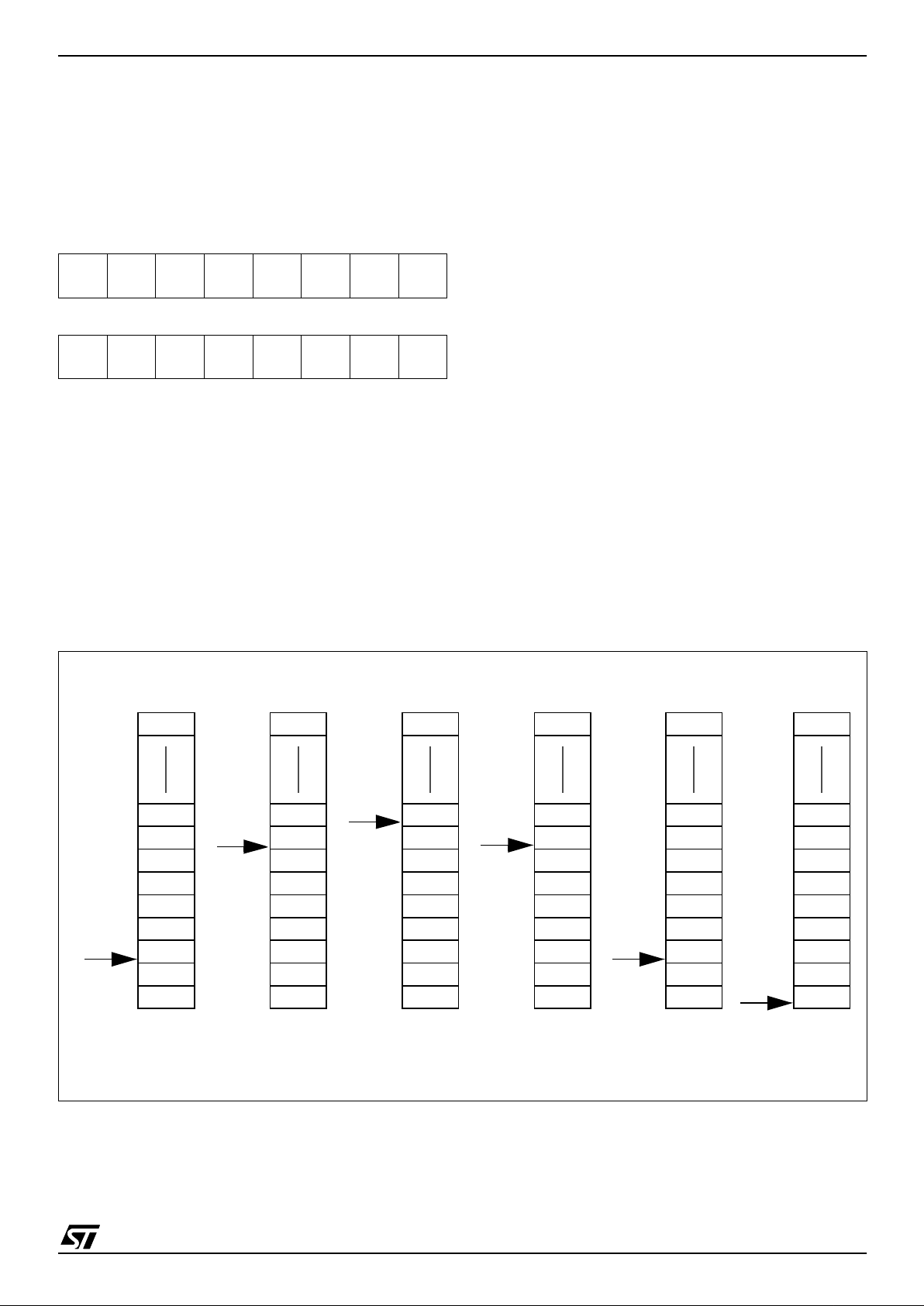
Stack Poi nter (SP)
Read/Write
Reset Value: 01 FFh
The Stack Pointer is a 16-bit register which is always pointing to the next free location in the stack.
It is then decremented after data has been pushed
onto the stack and incremented before data is
popped from the stack (see Figure 5).
Since the stack is 256 bytes deep, the 8 most significant bits are forced by hard ware. Following a n
MCU Reset, or after a Reset Stack Pointer instruction (RSP), the Stack Pointer contains its reset value (the SP7 to SP0 bits are set) which is the stack
higher address.
The least significant byte of the Stack Pointer
(called S) can be directly accessed by a LD instruction.
Note: When the lower limit is exceeded, the Stack
Pointer wraps around to the stack upper limit, without indicating the stack overflow. The previously
stored information is then o verwritten and therefore lost. The stack also wraps in case of an underflow.
The stack is used to sav e the return address during a subroutine call and the CPU context during
an interrupt. The user may also directly manipulate
the stack by means of the PUSH and POP instructions. In the case of an interrupt, the PCL is stored
at the first location po inted t o by t he SP. Th en t he
other registers are stored in the next locations as
shown in Figure 5.
– When an interrupt is received, the SP is decre-
mented and the context is pushed on the stack.
– On return from interrupt, the SP is incremented
and the context is popped from the stack.
A subroutine call occupies two locations and an interrupt five locat ion s i n the stack ar ea.
Figure 5. Stack Manipulation Example
15 8
00000001
70
SP7 SP6 SP5 SP4 SP3 SP2 SP1
SP0
PCH
PCL
SP
PCH
PCL
SP
PCL
PCH
X
A
CC
PCH
PCL
SP
PCL
PCH
X
A
CC
PCH
PCL
SP
PCL
PCH
X
A
CC
PCH
PCL
SP
SP
Y
CALL
Subroutine
Interrupt
Event
PUSH Y POP Y IRET
RET
or RSP
@ 01FFh
@ 0100h
Stack Higher Address = 01FFh
Stack Lower Address =
0100h
Page 16
ST72589BW, ST72389BW
16/158
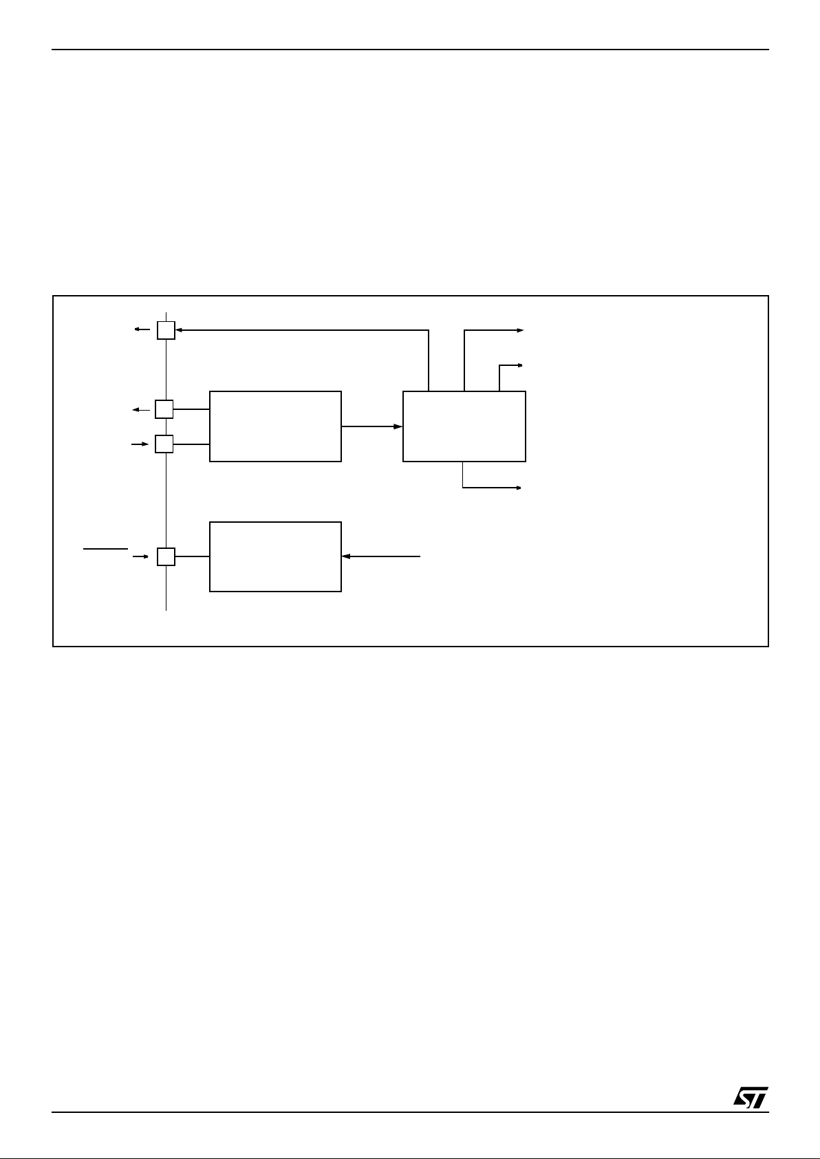
3 SUPPLY, RESET AND CLOCK MANAGE MENT
This chapter describes the following generic f eatures to guaranty the ST7 correct operation. An
overview is shown in Figure 6.
■ RESET Manager
■ Low Consum pti o n C ryst a l Os c illators
■ Main Clock controller (MCC)
Figure 6. Clock and RESET Management Overview
f
OSC
MAIN CLOCK
CONTROLLER
(MCC)
MAIN
OSCILLATOR
f
CPU
FROM
WATCHDOG
PERIPHERAL
MCC INTERRUPT
MCO
OSC1
OSC2
RESET
f
OSC
/2
RESET
Page 17

ST72589BW, ST72389BW
17/158
3.1 RESET MANAGER
3.1.1 Introd uc tion
There are three sources of Reset:
– RESET
pin (external source)
– Power-On Reset (internal source)
– WATCHDOG (internal source)
The Reset Service Routine vector is located at address FFFEh-FFFFh.
Figure 7. Reset Block Diagram
3.1.2 External Reset
The RESET
pin is both an input and an open-drain
output with integrated R
ON
weak pull-up resistor
(see Figure 7). This pull-up has not a fixed value
but varies in accordance with the input voltage. It
can be pulled low by external circuitry to reset th e
device.
A RESET signal originating from an external
source must have a duration of at least t
PULSE
in
order to be recognized. The RESET sequence associated to this RES ET s ource is shown in Fi gure
8.
When the RESET is generated by a internal
source, during the two first phases of the RESET
sequence, the device RE SET
pin acts as an out-
put that is pulled low.
Figure 8. External RESET Sequences
f
CPU
COUNTE R
RESET
R
ON
V
DD
WATCHDOG R ESET
POR
INTERNAL
RESET
RESET
RUN
INTERNAL RESET
4096 CLOCK CYCLES
FETCH
VECTOR
RUN
RESET PIN
EXTERNALRESET SOURCE
t
PULSE
WATCHDOGRESET
DELAY
Page 18

ST72589BW, ST72389BW
18/158
RESET MANAGER (Cont’d)
3.1.3 Internal Watchdog RESET
The RESET sequence generated by a internal
Watchdog counter underflow is reduced to 2 phases (see Figure 9).
Figure 9. Wat chdog RES E T Sequence
3.1.4 Reset Operation
The duration of the Reset condition, which is al so
reflected on the output pin, is fixed at 4096 internal
CPU Clock cycles. A Reset signal originating from
an external source must have a duration of at least
1.5 intern al CPU Clock cycles i n order to be recog nised. At the end of the Power-On Reset cycle, the
MCU may be held in the Reset condition by an External Reset signal. The RESET
pin may thus be
used to ensure V
DD
has risen to a point where the
MCU can operate correctly before the User program is run. Following a Reset event, or after exiting Halt mode, a 4096 CPU Clock cycle delay period is initiated in order to allow the oscillator to
stabilise and to ensure that recovery has taken
place from the Reset state.
During the Reset cycle, the device Reset pin acts
as an output that is pulsed low. In its high state, an
internal pull-up resistor is connected to the Reset
pin. This resistor can be pulled low by external circuitry to reset the device.
3.1.5 Power-on Reset
This circuit detects the ramping up of V
DD
, and
generates a pulse that is used to reset the application at V
POR
supply voltage.
Power-On Reset is desig ned exclusively to cope
with power-up conditions, and s houl d not be used
in order to attempt to detect a drop in the power
supply voltage.
Caution: to re-initialize the Power-On Reset, the
power supply voltage must fall below V
TN
, prior to
rise above V
POR
. If this condition is not respected,
on subsequent power-up the Reset pulse may not
be generated. An external Reset pulse may be required to correctly reactivate the circuit.
RESET
RUN
INTERNAL RESET
4096 CLOCK CYCLES
FETCH
VECTOR
RUN
RESET PIN
EXTERNALRESET SOURCE
WATCHDOGRESET
WATCHDOGUNDERFLOW
Page 19

ST72589BW, ST72389BW
19/158
3.2 LOW CONSUMPTION OSCILLATOR
The oscillator of the ST72589 and ST72389 devices is a Crystal/Ceramic Resonator Oscillator. Its
architecture is based on a constant current to minimize the consumption. It can be used either with
an external resonator or an external source.
This oscillator allows a high accuracy to supply the
clock for the ST7 CPU and its internal peripherals.
Using a Crystal/Ceramic Resonator
The resonator and the load capacitanc es have to
be connected as shown in Figure 10 and have t o
be mounted as c lose as pos sible to the o scillator
pins in order to minimize output distortion and
start-up stabilization time.
Figure 10. Main Crystal/Ceramic Resonator
Using an External Clock Source
In this mode, a square clock signal with ~50% duty
cycle has to drive the OSC1 pin while the OSC2
pin is tied to ground (see F igure 11).
Figure 11. Main External Clock Source
OSC1 OSC2
LOAD
CAPACITANCES
ST7
C
L2
C
L1
OSC1 O SC 2
EXTERNAL
ST7
SOURCE
Page 20

ST72589BW, ST72389BW
20/158
3.3 MAIN CLOCK CONTROLLER (MCC)
The MCC block supplies the clock for the ST7
CPU and its internal peripherals. It allows to m anage the power saving m odes such as the SLOW
and ACTIVE-HALT m odes . The whole functionality is managed by the Main Clock Control/Status
Register (MCCSR) and the M iscellaneous Register 2 (MISCR2).
The MCC block described in Figure 12 consists of:
– a programmable CPU clock prescaler
– a time base counter with inter rupt capabilit y
– a clock-out signal to supply external devices
The prescaler allows to select th e main clock frequency and is controlled with three bits of the
MCCSR: CP1, CP0 and SMS.
The counter allows to generate an interrupt based
on a accurate real time clock. Four different time
bases depending directly on f
OSC
are available.
The whole functionality is controlled by four bits of
the MCCSR register: TB1, TB0, OIE and OIF.
The clock-out capability allows to configure a dedicated I/O port pin as an f
OSC
/2 clock out to drive
external devices. It is controlled by a bit in the
MISCR2 register: MCO.
Figure 12. Main Clock Controller (MCC) Block Diagram
DIV 2, 4, 8, 16
MCC INTERRUPT
DIV 2
-
- -
TB1 TB0 OIE OIF
CPU CLOCK
MISCR2
PROGRAMMABLE
DIVIDER
CAN
TO CPU AND
PERIPHERALS
PERIPHERAL
f
OSC
f
CPU
MCO
PORT
FUNCTION
ALTERNATE
OSC1
OSC2
MAIN
OSCILLATOR
- --MCO-
0CP0CP1SMS
MCCSR
Page 21
ST72589BW, ST72389BW
21/158
MAIN CLOCK CONTROLLER (Cont’d)
MISCELLANEOUS REGISTER 2 (MISCR2)
See description in MISCELLANEOUS Register
Section.
MAIN CLOCK CONTROL/STATUS REGISTER
(MCCSR)
Read/Write
Reset Value: 0000 0000 (00h)
Bit 0 = SMS
Slow mode select
This bit is set and cleared by software.
0: Normal mode. f
CPU
= f
OSC
/ 2
1: Slow mode. f
CPU
is given by CP1, CP0
See low power consumption mode and MCC
chapters for more details.
Bit 2:1 = CP1-CP0
CPU clock prescaler
These bits select the CPU clock prescaler which is
applied in the different slow modes. Their action is
conditioned by the setting of the SM S bit. These
two bits are set and cleared by software
Bit 4 = R eserved , alway s read as 0.
Bit 3:2 = TB1-TB0
Time base control
These bits select the programmable divider time
base. They are set and cleared by software.
A mod ification of th e time base is tak en into account at the end of the current period (previously
set) to avoid unwanted time shift. This allows to
use this time base as a real time clock.
Bit 1 = OIE
Oscillator interrupt enable
This bit set and cleared by software.
0: Oscillator interrupt disable
1: Oscillator interrupt enable
This interrupt allows to exit from ACTIVE-HALT
mode. When this bit is set, calling the ST7 software HALT instruction accesses the ACTIVEHALT power saving mode.
Bit 0 = OIF
Oscillator interrupt flag
This bit is set by hardware and cleared by software
reading the CSR register. It indicates when set
that the main oscillator has measured the selected
elapsed time (TB1:0).
0: timeout not reached
1: timeout reached
Warning: BRES and BSET instructions must not
be used on the MCCS R register to avoid unwanted clearing of OIF bit.
70
SMS CP1 CP0 0 TB1 TB0 OIE OIF
f
CPU
in SLOW mode CP1 CP0
f
OSC
/ 4 0 0
f
OSC
/ 8 0 1
f
OSC
/ 16 1 0
f
OSC
/ 32 1 1
Counter
Prescaler
Time Base
TB1 TB0
f
OSC
=8MHz f
OSC
=16MHz
32000 4ms 2ms 0 0
64000 8ms 4ms 0 1
160000 20ms 10ms 1 0
400000 50ms 25ms 1 1
Page 22

ST72589BW, ST72389BW
22/158
MAIN CLOCK CONTROLLER (Cont’d)
Table 4. Main Clock Controller Register Map and Reset Values
Address
(Hex.)
Register
Label
76543210
0026h
MCCSR
Reset Value
SMS
0
CP1
0
CP0
00
TB1
0
TB0
0
OIE
0
OIF
0
Page 23
ST72589BW, ST72389BW
23/158
4 INTERRUPTS & POWER SAVING MODES
4.1 INTERRUPTS
4.1.1 Introd uc tion
The ST7 enhanced interrupt management provides the following features:
■ Hardware interrupts
■ Software interrupt (TRAP)
■ Nested or concurrent interrupt management
with flexible interrupt priority and level
management:
– Up to 4 software programmable nesting levels
– Up to 16 interrupt vectors fixed by hardware
– 3 non maskable events: NMI, RESET, TRAP
This interrupt management is based on:
– Bit 5 and bit 3 of the CPU CC register (I1:0),
– Interrupt software priority registers (ISPRx),
– Fixed interrupt vector addresses locat ed at the
high addresses of the memory map (FFE0h to
FFFFh) sorted by hardware priority order.
This enhanced interrupt cont roller guarantees full
upward compatibility with the standard (not nested) ST7 interrupt controller.
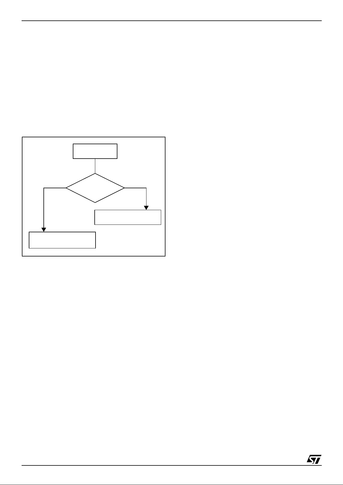
4.1.2 Interrupt Masking and Processing Flow
The interrupt masking is managed by the I1 and I0
bits of the CC register and the ISPRx registers
which give the interrupt software priority level of
each interrupt vector (see Table 5 ). The processing flow is shown in Figure 13
When an interrupt request has to be serviced:
– Normal processing is suspended at the end of
the current instruction execution.
– The PC, X, A and CC registers are saved onto
the stack.
– I1 and I0 bits of CC register are set according to
the corresponding values in the ISPRx registers
of the serviced interrupt vector.
– The PC is then loaded with the interrupt vector of
the interrupt to service and the first instruction of
the interrupt service routine is fetched (refer to
“Interrupt Mapping” table for vector addresses).
The interrupt service routine should end with the
IRET instruction which c auses the contents of the
saved registers to be recovered from the stack.
Note: As a consequence of the IRET instruction,
the I1 and I0 bits will be restored from the stack
and the program in the previous level will resume.
Table 5. Interrupt Software Priority Levels
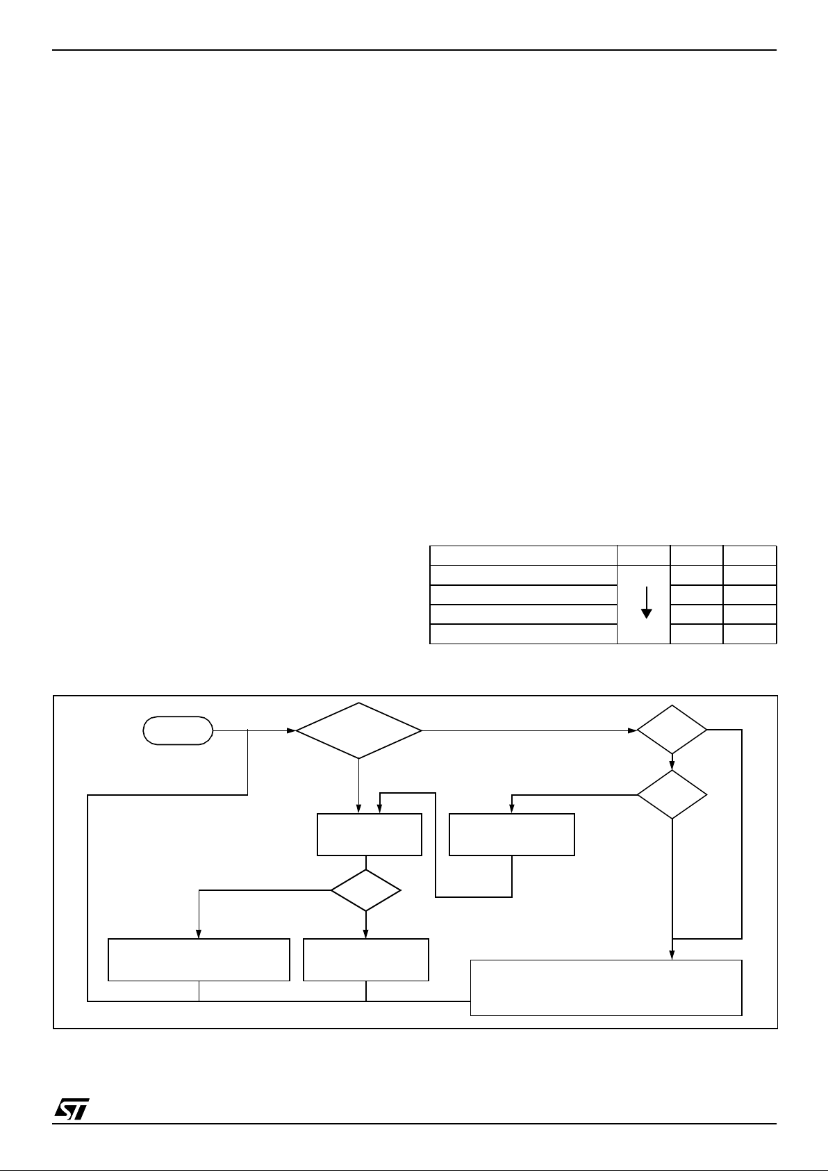
Figure 13. Int errupt Processing Flow c hart
Interrupt software priority Level I1 I0
Level 0 (main)
Low
High
10
Level 1 0 1
Level 2 0 0
Level 3 (= interrupt disable) 1 1
“IRET”
RESTORE PC, X, A, CC
STACK PC, X, A, CC
LOAD I1:0 FROM INTERRUPT SW REG .
FETCH NEX T
RESET
NMI
PENDING
INSTRUCTION
I1:0
FROM STACK
LOAD PC FROM INTERRUPT VECTOR
Y
N
Y
N
Y
N
Interrupt has the same or a
lower software priority
THE INTERRUPT
STAYS PENDING
than c u rrent one
Interrupt has a higher
softwarepriority
than current one
EXECUTE
INSTRUCTION
INTERRUPT
Page 24
ST72589BW, ST72389BW
24/158
INTERRUPTS (Cont’d)
Servicing Pending In te rrup t s
As several interrupts can b e pen ding at the s ame
time, the interrupt to be taken into account is determined by the following two-step process:
– the highest software priority interrupt is serviced,
– if several interrupts have the same software pri-
ority then the interrupt with the highest hardware
priority is serviced first.
Figure 14 describes this decision process.
Figure 14. Priority Decision Process
When an interrupt request is not serviced immediately, it is latched and then processed when its
software priority combined with the hardware priority becomes the highest one.
Note 1: The hardware priority is exclusive while
the software one i s not. This allows the prev ious
process to succeed with only one interrupt.
Note 2: RESET, TRAP and NMI are non maskable
and they can be considered as havin g the highest
software priority in the decision process.
Different Interrupt Vector Sources
Two interrupt source types are managed by the
ST7 interrupt controller: the non-maskable type
(RESET, NMI, TRAP) and t he maskable type (external or from internal peripherals).
Non-Maskable Sources
These sources are processed regardless of the
state of the I1 and I0 bits of the CC register (see
Figure 13). After stacking the PC, X, A and CC
registers (except for RESET), the corresponding
vector is loaded in the PC register and t he I1 and
I0 bits of the CC are set to disable interrupts (level
3). These sources allow the processor to exit
HALT mode.
■ NM I (Non Maskable Hardware Interrupt)
This hardware interrupt occurs when a specific
edge is detected on the dedicated NMI pin. Its detailed specification is given in the Miscellaneous
register chapter.
■ TRA P (Non Maskable Sof tware Interrupt)
This software interrupt is serviced when the TRAP
instruction is executed. It will be serviced according to the flowchart on Figure 13 as an NMI.
■ RE SET
The RESET source has the highest priority in the
ST7. This means that the first current routine has
the highest software priority (level 3) and the highest hardware priority.
See the RESET chapter for more details.
Maskable Sources
Maskable interrup t vector sourc es can be servi ced
if the corresponding in terrupt is enabled and if its
own interrupt software priority (in ISPRx registers)
is higher than the one currently being serviced (I1
and I0 in CC register). If any of these two co nditions is false, the interrupt is la tched and thus remains pending.
■ External Interrupts
External interrupts allow the processor to exit from
HALT low power mode.
External interrupt sensitivity is software selectable
through the Miscellaneous registers (MISCRx).
External interrupt triggered on edge will be latched
and the interrupt request automatically cleared
upon entering the interrupt service routine.
If several input pins of a group connected to the
same interrupt line are selected simultaneously,
these w ill be log i cally ORed.
■ Peripheral Interrupts
Usually the peripheral interrupts cause the MCU to
exit from HALT mode except thos e mentioned in
the “Interrupt Mapping” table.
A peripheral interrupt occurs when a specific flag
is set in the peripheral status registers and if the
corresponding enable bit is set in the peripheral
control register.
The general sequence for clearing an interrupt is
based on an access to the status register followed
by a read or write to an associated register.
Note: The clearing sequence resets the internal
latch. A pending interrupt (i.e. waiting for being
serviced) will therefore be lost if the clear sequence is executed.
PENDING
SOFTWARE
Different
INTERRUPTS
Same
HIGHEST HARDWARE
PRIORITY SERVICED
PRIORITY
HIGHEST SOFTWARE
PRIORITY SERVICED
Page 25
ST72589BW, ST72389BW
25/158
INTERRUPTS (Cont’d)
4.1.3 Interrupts and Low Power Modes
All interrupts allow the processor to exit the WAIT
low power mode. On the contrary, only external
and other specified interrupt s allow the processor
to exit the HALT modes (see column “Exit from
HALT” in “Interrupt Mapping” table). When several
pending interrupts are present while exiting HALT
mode, the first one serviced can only be an interrupt with exit from HALT mode capability and i t is
selected through the same decision process
shown in Figure 14
Note: If an interrupt, that is not able to Exit from
HALT mode, is pending with the highest priority
when exiting HALT mode, this interrupt is serviced
after the first one serviced.
4.1.4 Concurrent and Nested Interrupt
Management
The following Figure 15 and Figure 16 show two
different interrupt management modes. The first is
called concurrent mode and do es not allow an interrupt to be interrupted, unlike the nested mode in
Figure 16 The interrupt hardware priority is given
in this order from the l owes t to the hi ghest: M A IN,
IT4, IT3, IT2, IT1, IT0, NMI. The software priority is
given for each interrupt.
Warning: A stack overflow may occur without notifying the software of the failure.
Figure 15. Con c u rre n t int erru pt m anagemen t
Figure 16. Nested interrupt management
MAIN
IT4
IT2
IT1
NMI
IT1
MAIN
IT0
I1
HARDWARE PRIORITY
SOFTWARE
3
3
3
3
3
3/0
3
11
11
11
11
11
11 / 10
11
RIM
IT2
IT1
IT4
NMI
IT3
IT0
IT3
I0
10
PRIORITY
LEVEL
USED STACK = 10 BYTES
MAIN
IT2
NMI
MAIN
IT0
IT2
IT1
IT4
NMI
IT3
IT0
HARDWARE PRIORITY
3
2
1
3
3
3/0
3
11
00
01
11
11
11
RIM
IT1
IT4
IT4
IT1
IT2
IT3
I1 I0
11 / 10
10
SOFTWARE
PRIORITY
LEVEL
USED STACK = 20 BYTES
Page 26
ST72589BW, ST72389BW
26/158
INTERRUPTS (Cont’d)
4.1.5 Interrupt Register Description
CPU CC REGISTER INTERRUPT BITS
Read/Write
Reset Value: 111x 1010 (xAh)
Bit 5, 3 = I1, I0
Soft w a re In te r r u p t Priority
These two bits indicate the current interrupt software priority.
These two bits are set/cle ared by hardware whe n
entering in interrupt. The loaded value is given by
the corresponding bits in the interrupt software priority registers (ISPRx).
They can be also s et/cleared by s oft ware wi th the
RIM, SIM, HALT, WFI, IRET and PUSH/POP instructions (see “Interrupt Dedicated Instruction
Set” table).
*Note: NMI, TRAP and RESET events are non
maskable sources and can interrupt a level 3 program.
INTERRUPT SOFTWARE PRIORITY REGISTERS (ISPRX)
Read/Write (bit 7:4 of ISPR3 are read only)
Reset Values: 1111 1111 (FFh)
These four registers contain the interrupt software
priority of each interrupt vector.
– Each interrupt vector (except RESET and TRAP)
has corresponding bits in these registers where
its own software priority is stored. This correspondence is shown in the following table.
– Each I1_x and I0_x bit value in the ISPRx regis-
ters has the same meaning as the I1 and I0 bits
in the CC register.
– Level 0 can not be written (I1_x=1, I0_x=0). In
this case, the previously stored value is kept. (example: previous=CFh, write=64h, result=44h)
The RESET, TRAP and NMI vectors have no software priorities. When one is serviced, the I1 and I0
bits of the CC register are both set.
*Note: Bits in the ISPRx registers which correspond to the NMI can be read and written but they
are not significant in the interrupt process management.
Caution: If the I1_x and I0_x bits are modified
while the interrupt x is execu ted the following behaviour has to be considered: If the interrupt x is
still pending (new interrupt or flag not cleared) and
the new software priority is highe r than the previous one, the interrupt x is re-ent ered. Otherwise,
the software priority stays unchanged up to the
next interrupt request (after the IRET of the interrupt x).
70
11I1 H I0 NZC
Interrupt Software Priority Level I1 I0
Level 0 (main) Low
High
10
Level 1 0 1
Level 2 0 0
Level 3 (= interrupt disable*) 1 1
70
ISPR0 I1_3 I0_3 I1_2 I0_2 I1_1 I0_1 I1_0 I0_0
ISPR1 I1_7 I0_7 I1_6 I0_6 I1_5 I0_5 I1_4 I0_4
ISPR2 I1_11 I0_11 I1_10 I0_10 I1_9 I0_9 I1_8 I0_8
ISPR3 1 1 1 1 I1_13 I0_13 I1_12 I0_12
Vector address ISPRx bits
FFFBh-FFFAh I1_0 and I0_0 bits*
FFF9h-FFF8h I1_1 and I0_1 bits
... ...
FFE1h-FFE0h I1_13 and I0_13 bits
Page 27

ST72589BW, ST72389BW
27/158
INTERRUPTS (Cont’d)
Table 6. Dedicated Interrupt Instruc tion Set
Note: During the execution of an interrupt routine, the HALT, POPCC, RIM, SIM and WFI instructions change the current
software priority up to the next IRET instruction or one of the previously mentioned instructions.
In order not to lose the cu rrent so ftwar e priorit y level, the RIM, SIM, HA LT, WF I and PO P CC ins tructio ns sho uld nev er
be used in an interrupt routine.
Table 7. I nte rrupt Mapp in g
Instruction New Description Function/Example I1 H I0 N Z C
HALT Entering Halt mode 1 0
IRET Interrupt routine return Pop CC, A, X, PC I1 H I0 N Z C
JRM Jump if I1:0=11 I1:0=11 ?
JRNM Jump if I1:0<>11 I1:0<>11 ?
POP CC Pop CC from the Stack Mem => CC I1 H I0 N Z C
RIM Enable interrupt (level 0 set) Load 10 in I1:0 of CC 1 0
SIM Disable interrupt (level 3 set) Load 11 in I1:0 of CC 1 1
TRAP Software trap Software NMI 1 1
WFI Wait for interrupt 1 0
N°
Source
Block
Description
Register
Label
Priority
Order
Exit
from
HALT
Address
Vector
RESET Reset
N/A
Highest
Priority
Lowest
Priority
yes FFFEh-FFFFh
TRAP Software Interrupt no FFFCh-FFFDh
0 NMI External Non Maskable Interrupt MISCR1 yes FFFAh-FFFBh
1 EI1 External Interrupt Port A3..0
N/A
FFF8h-FFF9h
2 EI2 External Interrupt Port A7..4 FFF6h-FFF7h
3 EI3 External Interrupt Port B6..0 FFF4h-FFF5h
4 EI4 External Interrupt Port C7..0 FFF2h-FFF3h
5 EI5 External Interrupt Port D7..0 FFF0h-FFF1h
6 MCC Main Oscillator Time Base Interrupt MCCSR FFEEh-FFEFh
7 Not used FFECh-FFE Dh
8 CAN* CAN Peripheral Interrupts CANISR FFEAh-FFEBh
9 SPI SPI Peripheral Interrupts SPISR no FFE8h-FFE9h
10 TIMER A TIMER A Peripheral Interrupts TASR FFE6h-FFE7h
11 TIMER B TIMER B Peripheral Interrupts TBSR FFE4h-FFE5h
12 SCIP SCI Peripheral Interrupts SCISR FFE2h-FFE3h
13 I2C* I2C Peripheral Interrupts I2CSRx FFE0h-FFE1h
Page 28

ST72589BW, ST72389BW
28/158
INTERRUPTS (Cont’d)
Table 8. Nested Interrupts Register Map and Reset Values
Address
(Hex.)
Register
Label
76543210
001Ch
ISPR0
Reset Value
EI3 EI2 EI1 NMI
I1_3
1
I0_3
1
I1_2
1
I0_2
1
I1_1
1
I0_1
111
001Dh
ISPR1
Reset Value
ACC MCC EI5 EI4
I1_7
1
I0_7
1
I1_6
1
I0_6
1
I1_5
1
I0_5
1
I1_4
1
I0_4
1
001Eh
ISPR2
Reset Value
TIMER B TIMER A SPI CAN
I1_11
1
I0_11
1
I1_10
1
I0_10
1
I1_9
1
I0_9
1
I1_8
1
I0_8
1
001Fh
ISPR3
Reset Value1111
I2C SCI
I1_13
1
I0_13
1
I1_12
1
I0_12
1
Page 29

ST72589BW, ST72389BW
29/158
4.2 POWER SAVI N G MO DES
4.2.1 Introd uc tion
To give a large measure of flexibility to the application in terms of power consumption, four main
power saving modes are implemented in the ST7.
After a RESET the normal operating mode is selected by default (RUN mode). This mode drives
the device (CPU and embedded peripherals) by
means of a master clock which is based on the
main oscilla tor frequ ency divided by 2 (f
CPU
).
From Run mode, the different power saving
modes may be selected by setting the relevant
register bits or by calling the specific ST7 software
instruction whose action depends on the oscillator
status.
Figure 17. Power savi ng mode con sump tio n / transitions
4.2.2 HALT Modes
The HALT modes are the lowest power cons um ption modes of the MCU. They are en tered by executing the ST7 HALT instruction (see Figure 19).
Two different HALT modes can be distinguished:
– HALT : main os c illato r is turned of f,
– ACTIVE- HALT: only main oscillator is running.
The decision to enter either in HALT or AC TIVE-
HALT mode is given by the ma in osc illator enabl e
interrupt flag (OIE bit in CROSS-MCCSR register:
see Table 9).
When entering HALT modes, the I 1 and I 0 bits i n
the CC Register are forced to level 0 (“10”) to enable interrupts.
The MCU can exit HALT or ACTIVE-HALT modes
on reception of either an external interrupt, an in-
terrupt with Exit from Halt Mode capabi lity or a reset (see Table 2). A 4096 CPU clock cycles delay
is performed before the CPU operation resumes
(see Figure 18).
After the start up delay, the CPU resumes operation by servicing the interrupt or by fetching the reset vector which woke it up.
Table 9. HALT Modes selection
Figure 18. HALT /ACTIVE-HALT Modes timing overview
POWER CONSUMPTION
WAIT SLOW RUNHALT ACTIVE-HALT
High
Low
SLOW WAIT
MCCSR
OIE
flag
Power Saving Mode entered when HALT
instruction is execute d
0 HALT (reset if watchdog enabled)
1 ACTIVE-HALT (no reset if watchdog enabled)
HALT OR ACTIVE-HALT
RUN
RUN
4096 CPU CYCLE
DELAY
RESET
OR
INTERRUPT
HALT
INSTRUCTION
FETCH
VECTOR
Page 30

ST72589BW, ST72389BW
30/158
POWER SAVING MODES (Cont’d)
Standar d H ALT mode
In this mode the main os c illato r is turn ed off caus ing all internal processing to be stopped, including
the operation of the on-chip peripherals. All peripherals are not clocked except the ones which get
their clock supply from another clock generator
(such as an external oscillator).
The HALT instruction when executed while the
Watchdog system is enabled, generates a Watchdog RESET.
When exiting HALT m ode by means of a RESET
or an interrupt, the oscillator is immediately turned
on and the 4096 CPU cycle delay is used to stabilize the oscillator.
Specific ACTIVE-HALT mode
As soon as t he in terrupt capability of the mai n oscillator is selected (OIE bit set), the HALT instruction will make the device enter a specific ACTIVEHALT power saving m ode i nstead of th e sta ndard
HALT one.
This mode con sists of having o nly the m ain osc illator and its associated counter running to keep a
wake-up time base. All other peripherals are not
clocked except the ones which get their clock supply from another clock generator (such as external
oscillator).
The safeguard against staying locked in this ACTIVE-HALT mode is insured by the oscillator interrupt.
Note: As soon as the interrupt capability of the oscillators is selected (OIE bit set), entering in AC TIVE-HALT mode while the Watchdog is active
does not generate a RESET.
This means that the device cannot to s pend more
than a defined delay in this power saving mode.
Figure 19. HALT modes flow-chart
HALT INSTRUCTION
OSCILLATOR
1
0
CPU
OSCILLATOR
PERIPHERALS
I1 AND I0 BITS
ON
OFF
10
OFF
Notes:
OIE BIT
CPU
OSCILLATOR
PERIPHERALS
I1 AND I0 BITS
OFF
OFF
10
OFF
RESET
EXTERNAL*
Y
N
N
Y
CPU
OSCILLATOR
PERIPHERALS
ON
OFF
OFF
INTERRUPT
HALT
ACTIVE-HALT
MAIN
FETCH RESET VECTOR
OR SERVICE INTERRUPT**
4096 clock cy cl es delay
CPU
OSCI LLATOR
PERIPHERALS
ON
ON
ON
External interrupt or internal interrupts with Exit from Halt Mode capability
*
**
Before servicing an interrupt, the CC register is pushed on the stac k.
WATCHDOG
YN
ENABLE
Page 31

ST72589BW, ST72389BW
31/158
POWER SAVING MODES (Cont’d)
4.2.3 WAIT Mode
WAIT mode places the MCU in a low power c onsumption mode by stopping the CPU.
This pow e r s a v ing mo de is selected b y calling the
“WFI” ST7 software instruction.
All peripherals remain active. During WAIT mode,
the I1 and I0 bits of the CC register are forc ed to
level 0 (“10”), to enable all interr upts. All other registers and memory remain unchanged. The MCU
remains in WAIT mode until an interrupt or Reset
occurs, whereupon the P rogram Counter branc hes to the starting address of the interrupt or Reset
service routine.
The MCU will remain in WAIT m ode until a Reset
or an Interrupt occurs, causing it to wake up.
Refer to Figure 20.
Figure 20. WA I T m od e flow - chart
WFI INSTRUCTION
RESET
INTERRUPT
Y
N
N
Y
CPU
OSCILLATOR
PERIPHERALS
I1 AND I0 BITS
ON
ON
10
OFF
if exit caused by a RESET, a 4096 CPU
clock cycle delay is inserted.
CPU
OSCILLATOR
PERIPHERALS
ON
OFF*
OFF
Note:
*
The perip heral clock is st opped only when exit caused by RE SE T and not by an i nt errupt.
**
Before servicing an interrupt, the CC register is pushed on the stack.
FETCH RESET VECTOR
OR SERVICE INTERRUPT**
CPU
OSCILLATOR
PERIPHERALS
ON
ON
ON
Page 32

ST72589BW, ST72389BW
32/158
POWER SAVING MODES (Cont’d)
4.2.4 SLOW Mode
This mode has two targets:
– To reduce power consumption by decreasing the
internal clock in the device,
– To adapt the internal clock frequency (f
CPU
) to
the available supply voltage.
SLOW mode is controlled by three bits in the main
oscillator CSR register: the SMS bit which enables
or disables Slow mode and two CPx bits which select the internal slow frequency (f
CPU
).
In this mode, the oscillator frequency can be divided by 4, 8, 16 or 32 instea d of 2 in norm al ope rating mode. The CPU and peripherals (except CAN,
see Note) are clocked at this lower frequency.
Note: Before entering SLOW mode and in order to
guarantee low power operation, the CAN peripheral must be placed by software in STANDBY mode.
Figure 21. SLOW Mode: timing diagram for internal CPU clock transitions
00 01
01
SMS
CP1:0
f
CPU
f
OSC
/8
f
OSC
/4
NEW FREQUENCY
REQUEST
NEW FREQ UENCY
ACTIVE WHEN
OSC/4 & OSC/8 = 0
NORMA L M ODE
REQUEST
NORMA L MODE ACTIVE
(OSC/4, OSC/8 STOPPED)
MAIN
OSILLATOR
CSR
Page 33

ST72589BW, ST72389BW
33/158
5 I/O PORTS
5.1 INTRODUCTION
The I/O ports offer different functional modes:
– transfer of data through digital inputs and outputs
and for specific pins:
– ext ernal interrupt generation
– al terna te signal input/output for the on-chip pe-
ripherals.
An I/O port contains up to 8 pins. Each pin can be
programmed independently as digital input (with or
without interrupt generation) or digital output.
5.2 FUNCTIONAL DESCRIPTION
Each port has 2 main registers:
– Data Register (DR)
– Da ta Direction Register (DDR)
and one optional register:
– Option Register (OR)
Each I/O pin may be programmed using the corre-
sponding register bits in the DDR and OR registers: bit X corresponding to pin X of the port. The
same correspondence is used for the DR register.
The following description takes into account the
OR register, (for specific ports which do not provide this register refer to the I/O Port Im plement ation section). The generic I/O block diagram is
shown in Figure 1
5.2.1 Input Modes
The input configuration is s ele cted by clearing the
corresponding DDR register bit.
In this case, reading the DR register returns the
digital value applied to the external I/O pin.
Different input modes can be selected by software
through the OR register.
Notes:
1. Writing the DR register modifies t he latch v alu e
but does not affect the pin status.
2. When switching from input to output mode, the
DR register has to be written first to drive the correct level on the pin as soon as the port is configured as an output.
3. Do not use read/modify/write instructions (BSET
or BRES) to modify the DR register
External interrupt function
When an I/O is configured as Input with Interrupt,
an event on this I/O can generate an external interrupt request to the CPU.
Each pin can independent ly generate an interrupt
request. The interrupt sensitivity is independent ly
programmable using the sensitivity bits in the Miscellaneous register.
Each external interrupt vecto r is linked to a dedicated group of I/O port pins (see pinout description
and interrupt section). If several input pins are selected simultaneously as interrupt source, these
are logically NANDed. For this reason if one of the
interrupt pins is tied low, it masks the other ones.
In case of a floating input with interrupt configuration, special care must be taken when changing
the configuration (see Figure 2).
The external interrupts are hardware interrupts,
which means that the request latch (not accessible
directly by the application) is automatically cleared
when the corresponding interrupt vector is
fetched. To clear an unwanted pending interrupt
by software, the sensitivity bits in the Miscellaneous register must be modified.
5.2.2 Output Modes
The output configuration is selecte d by setting the
corresponding DDR register bit. In this case, writing the DR register applies this digital value to t he
I/O pin through the latch. Then reading the DR register returns the previously stored value.
Two different output modes can be selected by
software through the OR register: Output push-pull
and open-drain.
DR register value and output pin status:
5.2.3 Alternate Functions
When an on-chip peripheral is configured to use a
pin, the alternate function is au tomatically selected. This alternate function takes priority over the
standard I/O programming.
When the signal is coming from an on-chip peripheral, the I/O pin is autom ati cally conf igured in ou tput mode (push-pull or open drain according to the
peripheral).
When the signal is goi ng t o an on-c hip pe ripheral,
the I/O pin must be configured in input mode. In
this case, the pin state is also digitally readable by
addressing the DR register.
Note: Input pull-up configuration can cause unexpected value at the input of the alternate peripheral
input. When an on-chip peripheral use a pin as input and output, this pin h as to be configured in input floating mode.
DR Push-pull Open-drain
0V
SS
Vss
1V
DD
Floating
Page 34

ST72589BW, ST72389BW
34/158
I/O PORTS (Cont’d)
Figure 22. I /O Por t Ge nera l Blo c k D iag ram
Table 10. I/O Port M ode Options
Legend: NI - not implemented
Off - implemented not activated
On - implemented and activated
Note: The diode to V
DD
is not implemented in the
true open drain pads. A local protection between
the pad and V
SS
is implemented to protect the de-
vice against positive stress.
Configuration Mode Pull-Up P-Buffer
Diodes
to V
DD
to V
SS
Input
Floating with/without Interrupt Off
Off
On
On
Pull-up with/withou t Interrupt On
Output
Push-pull
Off
On
Open Drain (logic level) Off
True Open Drain NI NI NI (see note)
DR
DDR
OR
DATA BUS
PAD
V
DD
ALTERNATE
ENABLE
ALTERNATE
OUTPUT
1
0
OR SEL
DDR SEL
DR SEL
PULL-UP
CONFIGURATION
P-BUFFER
(see table below)
N-BUFFER
PULL-UP
(see table below)
1
0
ANALOG
INPUT
If implemented
ALTERNATE
INPUT
V
DD
DIODES
(see table below)
FROM
OTHER
BITS
EXTERNAL
SOURCE (eix)
INTERRUPT
POLARITY
SELECTION
CMOS
SCHMITT
TRIGGER
REGISTER
ACCESS
Page 35

ST72589BW, ST72389BW
35/158
I/O PORTS (Cont’d)
Table 11. I/O Port Configurations
Notes:
1. When the I/O port is in input configuration and the associated alternate function is enabled as an output,
reading the DR register will read the alternate func tion outp ut status.
2. When the I/O port is in output configuration and t he associated alternate function is enabled as an input,
the alternate function reads the pin status given by the DR register content.
Hardware Configuration
INPUT
1)
OPEN-DRAIN OUTPUT
2)
PUSH-PULL OUTPUT
2)
CONFIGURATION
PAD
V
DD
R
PU
EXTERNAL INTERRUPT
POLARITY
DATA BUS
PULL-UP
INTERRUPT
DR REGISTERACCESS
W
R
FROM
OTHER
PINS
SOURCE (ei
x
)
SELECTION
DR
REGISTER
CONF IGURATION
ALTERNATE INPUT
NOT I MPLEMENTED IN
TRUEOPEN DRAIN
I/O PO RTS
ANALOG INPUT
PAD
R
PU
DATA BUS
DR
DR REGISTER ACCESS
R/W
V
DD
ALTERNAT EALTERNATE
ENABLE OUTPUT
REGISTER
NOT IMPLEMENTED IN
TRUE OPEN DRAIN
I/O PORTS
PAD
R
PU
DATA BUS
DR
DR REGISTER ACCESS
R/W
V
DD
ALTERNAT EALTERNATE
ENABLE OUTPUT
REGISTER
NOT IMPLEMENTED IN
TRUE OPEN DRAIN
I/O PORTS
Page 36

ST72589BW, ST72389BW
36/158
I/O PORTS (Cont’d)
CAUTION: The alternate funct ion must not be ac -
tivated as long as the pin is configured as input
with interrupt, in order to avoid generating spurious
interrupts.
Analog alternate function
When the pin is used as an ADC input, the I/O
must be configured as floating input. Th e analog
multiplexer (controlled by the ADC registers)
switches the analog voltage present on the selected pin to the common analog rail which is connected to the ADC input.
It is recommended not to change the voltage level
or loading on any port pin while conversion is in
progress. Furthermore it is recommended not to
have clocking pins loca ted clos e to a s ele cted analog pin.
WARNING: The analog input voltage level must
be within the limits stated in the absolute maximum ratings.
5.3 I/O POR T IMPLEMENTATION
The hardware implementation on each I/O port depends on the settings in t he DDR and OR registers
and specific feature of the I/O port such as ADC Input or true open drain.
Switching these I/O ports from one state t o another should be done in a sequence that prevents unwanted side effects. Recommended safe transitions are illustrated in Figure 2 Other transitions
are potentially risky and shou ld be av oided, since
they are likely to present unwanted side-effects
such as spurious interrupt generation.
Figure 23. Interrupt I/O Port State Transitions
The I/O port register configurations are summarized as follows.
Standard I nte rrupt Ports
PA7:0, PB6:0, PC7:0, PD7:6, PD3:0
Open Drain Ports
PD5:4
Dedicated Configurations
Table 12. Port Configuration
MODE DDR OR
floating input 0 0
floating interrupt 0 1
open drain output 1 0
push-pull output 1 1
MODE DDR
floating input 0
open drain output 1
01
floating/pull-up
interrupt
INPUT
00
floating
(reset state)
INPUT
10
open-drain
OUTPUT
11
push-pull
OUTPUT
XX
= DDR, OR
Port Pin name
Input Output
OR = 0 OR = 1 OR = 0 OR = 1
Port A PA7:PA0
floating floating interrupt open drain push-pull
Port B PB6:PB0
Port C PC7:PC0
Port D
PD3:PD0
PD5:PD4 floating open-drain
PD7:PD6 floating floating interrupt open drain push-pull
Page 37

ST72589BW, ST72389BW
37/158
I/O P O R TS (Cont’d)
5.3.1 Register Description
DATA REGISTER (DR)
Port x Data Register
PxDR with x = A, B, C or D.
Read/Write
Reset Value: 0000 0000 (00h)
Bit 7:0 = D[7:0]
Data Register 8 bits.
The DR register has a specific behaviour according to the selected input/output configuration. Writing the DR register is always taken into account
even if the pin is configured as an input; this allows
to always have the expected level on the pin when
toggling to output mode. Reading the DR register
returns either the DR register latch content (pin
configured as output) or the digital value applied to
th e I /O pin (pi n configured as input).
DATA DIRECTION REGISTER (DDR)
Port x Data Direction Register
PxDDR with x = A, B, C or D.
Read/Write
Reset Value: 0000 0000 (00h)
Bit 7:0 = DD[7:0]
Data Direction Register 8 bits.
The DDR register gives the input/output direction
configuration of the pins. Each bits is set and
cleared by software.
0: Input mode
1: Output mode
OPTION REGISTER (OR)
Port x Option Register
PxOR with x = A, B, C or D.
Read/Write
Reset Value: 0000 0000 (00h)
Bit 7:0 = O[7:0]
Option Register 8 bits.
For specific I/O pins, this register is not implemented. In this case the DDR register is enough to select the I/O pin configuration.
The OR register allows to distinguish: in input
mode if the floating interrupt capability or the basic
floating configuration is selected, in output mode if
the push-pull or open drain configuration is selected.
Each bit is set and cleared by software.
Input mode:
0: floating input
1: floating input with interrupt
Output mode:
0: output open drain (with P-Buffer unactivated)
1: output push-pull
70
D7 D6 D5 D4 D3 D2 D1 D0
70
DD7 DD6 DD5 DD4 DD3 DD2 DD1 DD0
70
O7 O6 O5 O4 O3 O2 O1 O0
Page 38

ST72589BW, ST72389BW
38/158
I/O PORTS (Cont’d)
Table 13. I/O Port Register Map and Reset Values
Address
(Hex.)
Register
Label
76543210
Reset Value
of all IO port registers
00000000
0000h PADR
MSB LSB0001h PADDR
0002h PAOR
0004h PBDR
MSB LSB0005h PBDDR
0006h PBOR
0008h PCDR
MSB LSB0009h PCDDR
000Ah PCOR
000Ch PDDR
MSB LSB000Dh PDDDR
000Eh PDOR
Page 39

ST72589BW, ST72389BW
39/158
6 MISCELLANEOUS REGISTERS
The Miscellaneous registers allow control over
several features such as external interrupts or th e
I/O alternate functions.
6.1 I/O Port Interrupt Sensitivity Description
The external interrupt sensitivity is controlled by
the ISxx bits of the Miscellaneous registers (Figure
24). This control allows to have 2 fully independent
external interrupt source sensitivities.
Each external interrupt source can be generated
on four different events on the pin:
■ Falling edge
■ Rising edge
■ Falling and rising edge
■ Falling edge and low level
To guaranty the functionality, a modification of the
sensitivity in the MISCR registers can be done
only when the I1 and I0 bits of the CC register are
both set to 1 (level 3). See I/O port register and
Miscellaneous register descriptions for more details on the programming.
6.2 I/O Port Alternate Functions
The MISCR registers allow to manage three I/O
port miscellaneous alternate functions:
■ A Beep signal output on PC7 (with three
selectable audio frequencies)
■ A NMI manage men t on a dedicated pin
■ A SPI SS pin internal control to use the PD3 I/O
port function while the SPI is active.
These functions are described in details in the
Section 6.3 Miscellaneous Registers Description.
Figure 24. Extern al Interrupt So ur ces vs MIS CR
EI1
INTERRUPT
SOURCE
EI3
INTERRUPT
SOURCE
IS10IS11
MISCR1
SENSITIVITY
CONTROL
PA3
PA2
PA1
PA0
SOURCES
PB6
PB0
SOURCES
PD7
PD0
SOURCES
EI5
INTERRUPT
SOURCE
EI2
INTERRUPT
SOURCE
EI4
INTERRUPT
SOURCE
IS20 IS21
MISCR1
SENSITIVITY
CONTROL
PA7
PA6
PA5
PA4
SOURCES
PC7
PC0
SOURCES
Page 40

ST72589BW, ST72389BW
40/158
MISCELL ANE OUS REG ISTERS (Cont’d)
6.3 Miscellaneous Registers Description
MISCELLANEOUS REGISTER 1 (MISCR1)
Read/Write
Reset Value: 0000 0000 (00h)
Bit 7:6 = IS11-IS10
EI1,3, 5 Sensitivity
The selection issu ed from IS11,IS10 com bination
is applied to the following external interrupts: EI1
(port A3..0) EI3 (port B) and EI5 (port D).
These 2 bits can be written only when the current
interrupt software priority in the CC (Condition
Code) register is set to level 3 (I1:0=11).
Bit 5:4 = IS21-IS20
EI2,4 Sensitivity
The selection issu ed from IS21,IS20 com bination
is applied to the following external interrupts: EI2
(port A7..4) and EI4 (port C).
The functional description is equal to the IS1x one.
Bit 3:2 = Reserved, always read as 0.
Bit 1 = NMIS
NMI Sen sitivity
This bit allows to toggle the NMI edge sensitivity. It
can be set and cleared by software only when
NMIE bit is cleared.
0: falling edg e
1: rising edge
Bit 0 = NMIE
NMI Enable
This bit allows to enable or disable the NMI capability on the dedicated pin. It is set and cleared by
soft w ar e .
0: NMI disable
1: NMI enable
MISCELLANEOUS REGISTER 2 (MISCR2)
Read/Write
Reset Value: 0000 0000 (00h)
Bit 7 = Reserved.
Bit 6:4 = MCO
Main clock-out control
BC1-BC0
Beep Control
These 3 bits select the PC7 pin configuration.
They are set and cleared by software.
Note: the clock out and beep capabilities are not
available in HALT modes.
Bit 3:2 = Reserved, always read as 0.
Bit 1 = SSM
SS mode selection
It is set and cleared by software.
0: Normal mode - SS
uses information coming
from the SS
pin of the SPI.
1: I/O mode, the SP I uses the information stored
into bit SSI.
Bit 0 = SSI
SS internal mode
This bit replaces pin SS of the SPI when bit SSM is
set to 1. (see SPI description). It is set and cleared
by software.
70
IS11 IS10 IS21 IS20 0 0 NMIS NMIE
ISx1 ISx0 External Interrupt Sensitivity
0 0 Falling edge and low level
0 1 Falling edge only
1 0 Rising edge only
1 1 R ising and falling edge
70
0 MCO BC1 BC0 0 0 SSM SS I
MCO BC1 BC0 PC7 Configuration
0 0 0 Standard I/O
100 f
OSC
/2 Clock out
X 0 1 ~2-KHz
Output
Beep signal
w/ f
OSC
=16MHz
~50% duty cycle
X 1 0 ~1-KHz
X 1 1 ~500-Hz
Page 41

ST72589BW, ST72389BW
41/158
MISCELL ANE OUS REG ISTERS (Cont’d)
Table 14. Miscellaneo us Register M ap and Reset Value s
Address
(Hex.)
Register
Label
76543210
0020h
MISCR1
Reset Value
IS11
0
IS10
0
IS21
0
IS20
000
NMIS
0
NMI
0
0040h
MISCR2
Reset Value
0
MCO
0
BC1
0
BC0
000
SSM
0
SSI
0
Page 42

ST72589BW, ST72389BW
42/158
7 ON-CHIP PERIPHERALS
7.1 LCD DRIVER
7.1.1 Introd uc tion
The LCD driver controls up to 60 segments and 8
backplanes to drive up to 60x8 (480) or 60x4(240)
LCD segments.
Two programmable display modes (1/4 and 1/8
duty cycle) with 4 LCD drive frequencies can be
selected by software.
The parameters to d isplay are stored in a 60-byte
LCD dual port RAM.
Four different main oscillator clocks can be selected as clock for the peripheral.
– 8, 4, 2, 1 MHz f
CPU
software selectable.
The peripheral can be switched off by software to
reduce the power consumption while it is not used.
Figure 25. LCD Frequency Generator Block Diagram
7.1.2 Voltage references
The display voltage levels are supplied by an external resistor chain as shown in Figure 26 Th is
LCD driver needs 5 external voltage references
through 5 pins (GLCD, 1/4VLCD, 1/2VLCD,
3/4VLCD, VLCD).
The resistors used must have good tolerance
matching within 1% to avoid DC voltage levels on
the liquid crystal device. DC levels trigger electrode reactions in the li quid crystal cel l, causing a
rapid deterioration of the display quality.
Note: To avoid damaging the device, VLCD supply
voltages must always be supplied with more than
V
DD
or they have to be left unconnected.
Figure 26. LCD External Supply Network
CLOCK
DIVIDER
f
FR
f
LCDin
≈
16KHz
f
CPU
f
LCD
≈
0.5... 2 K Hz
DIV 8,16,24,32
DCS 0 CD1 CD0 LCDE 0 FS1 FS0
CR
BACKPL AN E
MUX
MAIN
OSCILLATOR
(SEG, CO M)
R
LCD
1
VLCD
EXTERNAL V
LCD
3/4VLCD
1/2VLCD
1/4VLCD
GLCD
R
LCD
2
R
LCD
3
R
LCD
4
C
LCD
1
C
LCD
2
C
LCD
3
Page 43

ST72589BW, ST72389BW
43/158
LCD DRIVER (Cont’d)
7.1.3 Segment and Common Output signals
Each dot of the LCD dot m atrix panel is turned on
when the differential voltage between the segment
signal and the common signal increases over a
certain threshold, it is turned off when the voltage
is below the threshold voltage. The common signals determine the select timing within a frame cycle (see Figure 27). The common signals have
similar waveforms to the segments, but different
phases.
Figure 27. Waveforms on LCD Outputs
Each common s ignal shows a high signal amplitude (VLCD-VSS) only at the correspon ding section of a frame time. At the ot her sections of the
frame, the signal amplitude is low (3/4VLCD-1/
4VLCD). A dot can be turned-on only at phases
with high signal amplitude.
In 1/8 duty cycle mode, one frame is divided into 8
sections, and each section is divided into two
phases, phase 0 and 1. In 1/4 duty cycle mode,
the number of sections is reduced to 4. This
means the waveform pat tern repeats fas ter in 1/4
duty cycle mode than 1/ 8 mode and the average
voltage and the ON/OFF duty cycle on a selected
pin is higher than in 1/8 mode. This results in a better contrast of the display.
Note: T he LCD must be disabled before enter ing
HALT mode or ACTIVE HALT mode.
Figure 28. LCD outputs with 1/8 Multiplex
V
LCD
3/4
1/2
1/4
GND
0101
Common selected
V
LCD
3/4
1/2
1/4
GND
0101
Common off
V
LCD
3/4
1/2
1/4
GND
0101
Segment selected
V
LCD
3/4
1/2
1/4
GND
0101
Segment off
V
LCD
3/4
1/2
1/4
GND
COM8
V
LCD
3/4
1/2
1/4
GND
COM7
V
LCD
3/4
1/2
1/4
GND
SEG1
V
LCD
3/4
1/2
1/4
GND
SEG2
8 765 218
ONE FRAME PERIOD
COM8
COM7
COM6
COM5
COM4
COM3
COM2
COM1
SEG1
SEG2
SEG3
SEG4
SEG5
SEG6
01010101 010101
Page 44

ST72589BW, ST72389BW
44/158
LCD DRIVER (Cont’d)
7.1.4 Register Description
LCD CONTROL REGISTER (CR)
Read/Write
Reset Value: 0000 0000 (00h)
Bit 7 = DCS
Duty cycle selection
This bit is set and cleared by software.
0: 1/4 duty cycle selected
1: 1/8 duty cycle selected
Bit 6 = Reserved, always read as 0.
Bit 5:4 = CD1,CD0
Clock divider
These bits allow to tune the f
LCDin
frequency to
~16KHz based on the selected f
CPU
.
These bits are set and cleared by software.
Bit 3 = L CDE
LCD enable
This bit is set and cleared by software.
0: LCD disable
1: LCD enable
While the LCD is disabled (LCDE bit cleared),
GLCD is applied to all Segment and Common
pins.
Bit 2 = Reserved, must be kept cleared.
Bit 1:0 = FS1,FS0
f
FR
Frame Frequency selection
These two bits allow to select the LCD frame frequency based on the f
LCDin
frequency and the selected duty cycle.
These bits are set and cleared by software.
The following table gives the possible LCD segment frequency (
f
LCD
) and LCD frame frequency
(
f
FR
) according to the selected duty cycle.
With
f
LCDin
=15625Hz (main oscillator)
70
DCS 0 CD1 CD0 LCDE 0 FS1 FS0
f
LCDin
f
CPU
Divider CD1 CD0
15625Hz
8-MHz 1/512 0 0
4-MHz 1/256 1 1
2-MHz 1/128 1 0
1-MHz 1/64 0 1
f
LCDin
Ratio
f
LCD
f
FR
FS1 FS0
1/4 d.c. 1/8 d.c.
1/8 1953-Hz 488-Hz 244-Hz 0 0
1/16 977-Hz 244-Hz 122-Hz 0 1
1/24 651-Hz 163-Hz 81-Hz 1 0
1/32 488-Hz 122-Hz 61-Hz 1 1
Page 45

ST72589BW, ST72389BW
45/158
LCD DRIVER (Cont’d)
LCD RAM DESCRIPTION
The LCD RAM is loc ated in the dat a spac e in on e
page of 60 bytes. Each bit of the LCD RAM is
mapped to one dot of the LCD matrix. If a bit is set,
the corresponding LCD dot is switched on, else
the dot is switched off.
After reset, the LCD RAM is not ini tialized and contains arbitrary information.
The bit position of the selected bit in the LCD RAM byte gives the common data. The segment data is given by the LCD RAM relative address.
Table 15. LCD Driver Register Map and Reset Values
LCD RAM Bit position 7 6 5 4 3 2 1 0
LCD Common COM8 COM7 COM6 COM5 COM4 COM3 COM2 COM1
LCD RAM Relative address 00h 01h 02h
...................
39h 3Ah 3Bh
LCD Segment S1 S2 S3 S58 S59 S60
Address
(Hex.)
Register
Label
76543210
0058h
LCDCR
Reset Value
DCS
00
CD1
0
CD0
0
LCDE
00
FS1
0
FS0
0
0480h
to
04BBh
LCDRAM
Reset Value
Seg X
Com8
X
Seg X
Com7
X
Seg X
Com6
X
Seg X
Com5
X
Seg X
Com4
X
Seg X
Com3
X
Seg X
Com2
X
Seg X
Com1
X
Page 46

ST72589BW, ST72389BW
46/158
7.2 WATCHDOG TIMER (WDG)
7.2.1 Introd ucti on
The Watchdog t imer is used to d etect the occurrence of a software fault, usually generated by external interference or by unforeseen logical conditions, which causes the application program to
abandon its normal seque nce. The W atchdog circuit generates an MCU reset on expiry of a programmed time period, unless the program refresh-
es the counter’s contents before the T6 bit becomes cleared.
7.2.2 Main Features
■ Programmable timer (64 increments of 12288
CPU cycles)
■ Programmable reset
■ Reset (if watchdog activated) after a HALT
instruction or when the T6 bit reaches zero
Figure 29. Watchdog Block Diagra m
RESET
WDGA
7-BIT DOWNCOU NTE R
f
CPU
T6 T0
CLOCK DIVIDER
WATCHDOG CONTROL REGISTER (CR)
÷
12288
T1
T2
T3
T4
T5
Page 47

ST72589BW, ST72389BW
47/158
WATCH DOG TI MER (Cont’d)
7.2.3 Functional Descript ion
The counter value stored in the CR register (bits
T6:T0), is decremented every 12,288 machine cycles, and the length of the timeout period can b e
programmed by the user in 64 increments.
If the watchdog is activated (the W DGA bit is set)
and when the 7-bit timer (bits T6:T0) rolls over
from 40h to 3Fh (T6 becom es cleared), it initiates
a reset c ycle p ullin g lo w t he res et pi n f or typica lly
500ns.
The application program must write in the CR register at regular intervals during normal operation to
prevent an MCU reset. The valu e to be stored in
the CR register must be between FFh and C0h
(see Table 16 . Watchdog Timing (fCPU = 8
MHz)):
– T he WDGA bit is set (watchdog enabled)
– The T6 bit is set to prevent generating an imme-
diate reset
– The T5:T0 bits contain the number of increments
which represents the time delay before the
watchdog produces a reset.
Table 16. Watchdog Timing (f
CPU
= 8 MHz)
Notes: Following a reset, the watchdog is disa-
bled. Once activated it cannot be disabled, except
by a reset.
The T6 bit can be used t o generate a s of tw are reset (the WDGA bit is set and the T6 bit is cleared).
If the watchdog is activated, the HALT instruction
will generate a Reset.
7.2.4 Low Power Mo des
7.2.5 Interrupts
None.
7.2.6 Register Description
CONTROL REGISTER (CR)
Read/Write
Reset Value: 0111 1111 (7Fh)
Bit 7 = WDGA
Activation bit
.
This bit is set by software and only cleared by
hardware after a reset. When WDGA = 1, the
watchdog can generate a reset.
0: Watchdog disabled
1: Watchdog enabled
Bit 6:0 = T[6:0]
7-bit timer (MSB to LSB).
These bits contain the decremented value. A reset
is produced when it rolls over from 40h to 3Fh (T6
becomes cleared).
CR Register
initial value
WDG timeout period
(ms)
Max FFh 98.304
Min C0h 1.536
Mode Description
WAIT No effect on Watchdog.
HALT
Immediate reset generation as soon as
the HALT instruction is executed if the
Watchdog is activated (WDGA bit is
set).
70
WDGA T6 T5 T4 T3 T2 T1 T0
Page 48

ST72589BW, ST72389BW
48/158
WATCH DOG TI MER (Cond ’t)
Table 17. Watchdog Time r Register Map and Rese t Values
Address
(Hex.)
Register
Label
76543210
0024h
WDGCR
Reset Value
WDGA
0
T6
1
T5
1
T4
1
T3
1
T2
1
T1
1
T0
1
Page 49

ST72589BW, ST72389BW
49/158
7.3 16-BIT TIMER
7.3.1 Introd ucti on
The timer consists of a 16-bit free-running counter
driven by a programmable prescaler.
It may be used for a variety of purposes, including
measuring the pulse lengths of up to two input signals (
input capture
) or generating up to two output
waveforms (
output compare
and
PWM
).
Pulse lengths and wave form periods can be modulated from a few microseconds to several milliseconds using the timer prescaler and the CPU
clock prescaler.
Some ST7 devices have two on-chip 16-bit t imers.
They are completely independent, and do not
share any resources. They are synchronized a fter
a MCU reset as long as the timer clock frequencies are not modified.
This description covers one or two 16-bit timers. In
ST7 devices with two tim ers, register names are
prefixed with TA (Timer A) or TB (Timer B).
7.3.2 Main Features
■ Programmable prescaler: f
CPU
divided by 2, 4 or 8.
■ Overflow status flag and maskable interrupt
■ External clock input (must be at least 4 times
slower than the CPU
clock speed) with the choice
of active edge
■ Output compare functions with:
– 2 dedicated 16-bit registers
– 2 dedicated programma ble signal s
– 2 dedicated status flags
– 1 dedicated maskable interrupt
■ Input capture functions with:
– 2 dedicated 16-bit registers
– 2 dedicated active edge selection signals
– 2 dedicated status flags
– 1 dedicated maskable interrupt
■ Pulse Width Modulation mode (PWM)
■ One Pulse mode
■ 5 alternate functions on I/O ports (ICAP1, ICAP2,
OCMP1, OCMP2, EXTCLK)*
The Block Diagram is shown in Figure 30.
*Note: Some timer pin s m ay not be av ai lable (not
bonded) in some ST7 devices. Refer to the device
pin out description.
When reading an input signal on a non-bonded
pin, the value will always be ‘1’.
7.3.3 Functional Description
7.3.3.1 Counter
The main block of the Programmable Timer is a
16-bit free running upcounter and its associated
16-bit registers. The 16-bit registers are made up
of two 8-bit registers called high & low.
Counter Register (CR):
– Counter High R egister (CHR) is the most sig-
nifican t b y te (MS B yte).
– Counter Lo w Register (CLR) is the least sig-
nificant byte (LS Byte).
Alternate Counter Register (ACR)
– Alternate Counter H igh Re gist er (ACH R) is t he
most significant byte (MS Byte).
– Alternate Counter Low Register (ACLR) is the
least significant byt e (LS Byte).
These two read-only 16-bit registers contain the
same value but with the difference that reading the
ACLR register does not clear the TOF bit (Timer
overflow flag), located in the St atus register (SR).
(See note at the end of paragraph titled 16-bit read
sequence).
Writing in the CLR register or ACLR register reset s
the free running counter to the FFFCh value.
Both counters have a reset value of FFFCh (this is
the only value which is reloaded in the 16-bit timer). The reset value of both counters is also
FFFCh in One Pulse mode and PWM mode.
The timer clock depends on th e clock control bits
of the CR2 register, as illustrated in Table 18 Clock
Control Bits. The value in the counter regi ster re-
peats every 131072, 262144 or 524288 CPU clock
cycles depending on the CC[1:0] bits.
The timer frequency can be f
CPU
/2, f
CPU
/4, f
CPU
/8
or an external frequency.
Page 50

ST72589BW, ST72389BW
50/158
16-B IT TIMER (Cont’d)
Figure 30. Timer Block Diagram
MCU-PERIPHERAL INTERFACE
COUNTER
ALTERNATE
OUTPUT
COMPARE
REGISTER
OUTPUT COMPARE
EDGE DETECT
OVERFLOW
DETECT
CIRCUIT
1/2
1/4
1/8
8-bit
buffer
ST7 INTERNAL BUS
LATCH1
OCMP1
ICAP1
EXTCLK
f
CPU
TIMER INTERRUPT
ICF2ICF1 000OCF2OCF1 TOF
PWMOC1E
EXEDG
IEDG2CC0CC1
OC2E
OPMFOLV2ICIE OLVL1IEDG1OLVL2FOLV1OCIE TOIE
ICAP2
LATCH2
OCMP2
8
8
8 low
16
8 high
16 16
16
16
(Control Register 1) CR1
(Control Register 2) CR2
(Status Register) SR
6
16
8 8 8
88 8
high
low
high
high
high
low
low
low
EXEDG
TIMER INTERNAL BUS
CIRCUIT1
EDGE DETECT
CIRCUIT2
CIRCUIT
1
OUTPUT
COMPARE
REGISTER
2
INPUT
CAPTURE
REGISTER
1
INPUT
CAPTURE
REGISTER
2
CC[1:0]
COUNTER
pin
pin
pin
pin
pin
REGISTER
REGISTER
Note: If IC, OC and TO interrupt requests have separate vectors
then the last OR is not present (See device Interrupt Vector Tabl e)
(See note)
Page 51

ST72589BW, ST72389BW
51/158
16-B IT TIMER (Cont’d)
16-bit Read Sequence: (from either the Counter
Register or the Alternate Counter Register).
The user must read the MS Byte first, then the LS
Byte value is buffered automatically.
This buffered val ue remains unchanged until the
16-bit read sequence is completed, even if the
user reads the MS Byte several times.
After a complete reading sequence, if only the
CLR register or ACLR register are read, they return the LS Byte of the c ount value at the time of
the read.
Whatever the timer mode used (input capture, output compare, One Pul se mo de or P WM m ode) an
overflow occurs when the counter rolls over from
FFFFh to 0000h then:
– T he TOF bit of the SR register is set.
– A timer interrupt is generated if:
– TOIE bit of the CR1 register is set and
– I bit of the CC register is cleared.
If one of these conditions is false, the interrupt remains pending to be issued as soon as they are
both true.
Clearing the overflow interrupt request is done in
two steps:
1.Reading the SR register while the TOF bit is set.
2.An access (read or write) to the CLR register.
Note: The TOF bit is not cleared by accessing the
ACLR register. The advantage of accessing the
ACLR register rather than the CLR register is that
it allows simultaneous use of the overflow function
and reading the free running counter at random
times (for example, to measure elapsed time) without the risk of clearing the TOF bit erroneously.
The timer is not affected by WAIT mode.
In HALT mode, the counter stops counting until the
mode is exited. Counting then resumes from the
previous count (MCU awakened by an interrupt) or
from the reset count (MCU awakened by a Reset).
7.3.3.2 External Clock
The external clock (where available) is selected if
CC0=1 and CC1=1 in the CR2 register.
The status of the EXEDG bit in the CR2 register
determines the type of level transition on the external clock pin EXTCLK that will trigger the free running counter.
The counter is synchroni sed with the falling edge
of the internal CPU clock.
A minimum of four falling edges of the CPU c lock
must occur between two consecutive active edges
of the external clock; t hus the external clock frequency must be less than a quarter of the CPU
clock frequency.
is buffered
Read
At t0
Read
Returns the buffered
LS Byte value at t0
At t0 +∆t
Other
instructions
Beginning of the sequence
Sequence completed
LS Byte
LS Byte
MS Byte
Page 52

ST72589BW, ST72389BW
52/158
16-B IT TIMER (Cont’d)
Figure 31. Counter Timing Diagram, internal clock divided by 2
Figure 32. Counter Timing Diagram, internal clock divided by 4
Figure 33. Counter Timing Diagram, internal clock divided by 8
Note: The MCU is in reset state when the internal reset signal is high. When it is low, the MCU is running.
CPU CLOCK
FFFD FFFE FFFF 0000 0001 0002 0003
INTERNAL RESET
TIMER CLOCK
COUNTER REGISTER
TIMER OVERFL OW FLAG (TOF)
FFFC FFFD 0000 0001
CPU CLOCK
INTERNAL RESET
TIMER CLOCK
COUNTER REGI STER
TIMER OVERFLOW FLAG (TOF)
CPU CLOCK
INTERNAL RESET
TIMER CLOCK
COUNTER REGISTER
TIMER OVERFLOW FLAG (TOF)
FFFC FFFD
0000
Page 53

ST72589BW, ST72389BW
53/158
16-B IT TIMER (Cont’d)
7.3.3.3 Input Capture
In this section, the index,
i
, may be 1 or 2 because
there are 2 input capture functions in the 16-bit
timer.
The two input capture 16-bit registers (IC1R and
IC2R) are used to latch the v alue of the free running counter after a transition is detected by the
ICAP
i
pin (see figure 5).
The IC
i
R register is a read-only register.
The active transition is software programmable
through the IEDG
i
bit of Control Registers (CRi).
Timing resolution is one count of the free running
counter: (
f
CPU
/CC[1:0]).
Procedure:
To use the input capture function, select the following in the CR2 register:
– Select the timer clock (CC[1:0]) (see Table 18
Clock Control Bits).
– Select the edge of the active transition on the
ICAP2 pin with the IEDG2 bit (the ICAP2 pin
must be configured as a floating input or input
with pull-up without interrupt if this c onfiguration
is available).
And select the following in the CR1 register:
– Set the IC IE b it to ge nerate an in terrupt after a n
input capture com ing from e ither the I CAP1 pin
or the ICAP2 pin
– Select the edge of the active transition on the
ICAP1 pin with the IEDG1 bit (the ICAP1 pin
must be configured as a floating input or input
with pull-up without interrupt if this c onfiguration
is available).
When an input capture occurs:
– The ICF
i
bit is set.
– The IC
i
R register contains the v alue of the free
running counter on the active transition on the
ICAP
i
pin (see Figure 35).
– A timer interrupt is generated if the ICIE bit i s s et
and the I bit is cleared in the CC register. Otherwise, the interrupt remains pending until both
conditions become true.
Clearing the Input Capture interrupt request (i.e.
clearing the ICF
i
bit) is done in two steps:
1. Reading the SR register while the ICF
i
bit is set.
2. An access (read or write) to the IC
iLR
register.
Notes:
1. After reading the IC
i
HR register, the transfer of
input capture data is inhibited and ICF
i
will
never be set until the IC
i
LR register is also
read.
2. The IC
i
R register contains the free running
counter value which corresponds to the most
recent input capture.
3. The 2 input capture functions can be used
together even if the timer also uses the 2 output
compare functions.
4. In One Pulse mode and PWM mode only the
input capture 2 function can be used.
5. The alternate inputs (ICAP1 & ICAP2) are
always directly con nected to the timer. So any
transitions on these pins activate the input capture function.
Moreover if one of th e ICAP
i
pin is configured
as an input and t he second one as an output,
an interrupt can be generated if the user toggles the output pin and if the ICIE bit is set.
This can be avoided if the input capture function
i
is disabled by reading the ICiHR (see note
1).
6. The TOF bit can be used with an interrupt in
order to measure events that ex ceed the timer
range (FFFFh).
MS Byte LS Byte
ICiR IC
i
HR ICiLR
Page 54

ST72589BW, ST72389BW
54/158
16-B IT TIMER (Cont’d)
Figure 34. Input Capture Block Diagram
Figure 35. Input Capture Timing Diagram
ICIE
CC0
CC1
16-BIT FREE RUNNING
COUNTER
IEDG1
(Control Register 1) CR1
(Control Register 2) CR2
ICF2ICF1 000
(Status Register) SR
IEDG2
ICAP1
ICAP2
EDGE DETECT
CIRCUIT2
16-BIT
IC1R Register
IC2R Register
EDGE DETECT
CIRCUIT1
pin
pin
FF01 FF02 FF03
FF03
TIMER CLOCK
COUNTER REGISTER
ICAPi PIN
ICAPi FLAG
ICAPi REGISTER
Note: Active edge is rising edge.
Page 55

ST72589BW, ST72389BW
55/158
16-B IT TIMER (Cont’d)
7.3.3.4 Output Compare
In this section, the index,
i
, may be 1 or 2 because
there are 2 output compare functions in the 16-bit
timer .
This function can be used to control an output
waveform or indicate when a period of time has
elapsed.
When a match is fou nd bet ween the Output Com pare register and the free running counter, the output compare function:
– Assigns pins with a programmable value if the
OC
i
E bit is se t
– Sets a flag in the status register
– Generates an interrupt if enabled
Two 16-bit registers Output Compare Register 1
(OC1R) and Output Compare Register 2 (OC2R)
contain the value to be c ompared to the counter
register each timer clock cycle.
These registers are readable and writable and are
not affected by the timer hardware. A reset event
changes the OC
i
R value to 8000h.
Timing resolution is one count of the free running
counter: (
f
CPU/
CC[1:0]
).
Procedure:
To use the output compare function, select the following in the CR2 register:
– S et the OC
i
E bit if an output is needed then the
OCMP
i
pin is dedica ted to the output c ompare
i
signal.
– Select the timer clock (CC[1:0]) (see Table 18
Clock Control Bits).
And select the following in the CR1 register:
– Select the OLVL
i
bit to applied to the OCMPi pins
after the match occurs.
– Set the O CIE bit to generate an interrupt if it is
needed.
When a match is found between OCRi register
and CR register:
– OCF
i
bit is set.
– The OCMP
i
pin takes OLVLi bit value (OCMPi
pin latch is forced low during reset).
– A timer interrupt is generated if the OCIE bit is
set in the CR1 register and the I bit is cleared in
the CC register (CC).
The OC
i
R register value required for a specific timing application can be calculated using the following f ormula:
Where:
∆t = Output compare period (in seconds)
f
CPU
= CPU clock frequency (in hertz)
PRESC
= Timer prescaler factor (2, 4 or 8 de-
pending on CC[1:0] bits, see Table 18
Clock Control Bits)
If the timer clock is an external clock, the formula
is:
Where:
∆t = Output compare period (in seconds)
f
EXT
= External timer clock frequency (in hertz)
Clearing the output compare interrupt request (i.e.
clearing the OCF
i
bit) is done by:
1. Reading the SR register while the OCF
i
bit is
set.
2. An access (read or write) to the OC
i
LR register.
The following procedure is recommended to prevent the OCF
i
bit from being set between the time
it is read and the write to the OC
i
R register:
– Write to the OC
i
HR register (further compares
are inhibited).
– Read the SR register (first step of the clearance
of the OCF
i
bit, which may be already set).
– Write to the OC
i
LR register (enables the output
compare function and clears the OCF
i
bit).
MS Byte LS Byte
OC
i
ROC
i
HR OCiLR
∆ OC
i
R =
∆t * f
CPU
PRESC
∆ OC
i
R = ∆t
* fEXT
Page 56

ST72589BW, ST72389BW
56/158
16-B IT TIMER (Cont’d)
Notes:
1. After a process or write cycle to the OC
iHR
register, the output compare function is inhibited
until the OC
iLR
register is also written.
2. If the OC
i
E bit is not set, the OCMPi pin is a
general I/O port and the OLVL
i
bit will not
appear when a match is found but an interrupt
could be generated if the OCIE bit is set.
3. When the timer clock is f
CPU
/2, OCFi and
OCMP
i
are set while the counter value equals
the OC
i
R register value (see Figure 37). This
behaviour is the same in OPM or PWM mode.
When the timer clock is f
CPU
/4, f
CPU
/8 or in
external clock mode , OCF
i
and OCMPi are set
while the counter value equals the OC
i
R regis-
ter value plus 1 (see Figure 38).
4. The output compare functions can be used both
for generating external events on the OCMP
i
pins even if the input capture mode is also
used.
5. The value in the 16-bit OC
i
R register and the
OLV
i
bit should be changed after each successful comparison in order to control an output
waveform or establish a new elapsed timeout.
Forced Compare Output capab ility
When the FOLV
i
bit is set by software, the OLVL
i
bit is copied to the OCMPi pin. The OLVi bit has to
be toggled in o rder t o t oggle the OCMP
i
pin when
it is enabled (OC
i
E bit=1). The OCFi bit is then not
set by hardware, and thus no interrupt request is
generated.
FOLVL
i
bits have no effect in either One-Pulse
mode or PWM mode.
Figure 36. Output Compare Block Diagram
OUTPUT COMPARE
16-bit
CIRCUIT
OC1R Register
16 BIT FREE RUNNING
COUNTER
OC1E CC0CC1
OC2E
OLVL1OLVL2OCIE
(Control Register 1) CR1
(Control Register 2) CR2
000OCF2OCF1
(Status Register) SR
16-bit
16-bit
OCMP1
OCMP2
Latch
1
Latch
2
OC2R Register
Pin
Pin
FOLV2 FOLV1
Page 57

ST72589BW, ST72389BW
57/158
16-B IT TIMER (Cont’d)
Figure 37. Output Compare Timing Diagram, f
TIMER
=f
CPU
/2
Figure 38. Output Compare Timing Diagram, f
TIMER
=f
CPU
/4
INTERNAL CPU CLOC K
TIMER CLOCK
COUNTER REGISTER
OUTPUT COMPARE REGISTER
i
(OCRi)
OUTPUT COMPARE FLAG
i
(OCFi)
OCMP
i
PIN (OLVLi=1)
2ED3
2ED0 2ED1 2ED2
2ED3
2ED42ECF
INTERNAL CPU CLOC K
TIMER CLOCK
COUNTER REGISTER
OUTPUT COMPARE REGISTER
i
(OCRi)
COMPARE REGISTER
i
LATCH
2ED3
2ED0 2ED 1 2ED2
2ED3
2ED42ECF
OCMPi PIN (OLVLi=1)
OUTPUT COMPARE FLAG
i
(OCFi)
Page 58

ST72589BW, ST72389BW
58/158
16-B IT TIMER (Cont’d)
7.3.3.5 One Pulse Mode
One Pulse mode enables the generation of a
pulse when an external event occurs. This mode is
selected via the OPM bit in the CR2 register.
The One Pulse mode uses the Input Capture1
function and the Output Compare1 function.
Procedure:
To use One Pulse mode:
1. Load the OC1R register with the value corresponding to the length of the pulse (see the formula in the opposite column).
2. Select the following in the CR1 register:
– Using the OLVL1 bit, select the level to be ap-
plied to the OCMP1 pin after the pulse.
– Using the OLVL2 bit, select the level to be ap-
plied to the OCMP1 pin during the pulse.
– Select the edge of the active transition o n th e
ICAP1 pin with the IEDG1 bit
(the ICAP1 pin
must be configured as floating input).
3. Select the following in the CR2 register:
– Set the OC1E bit, the OCMP1 pin is then ded-
icated to the Output Compare 1 function.
– Set the OPM bit.
– Select the timer clock CC[1:0] (see Table 18
Clock Control Bits).
Then, on a valid event on the ICAP1 pin, the counter is initialized to FFFCh and the OLVL2 bit is
loaded on the OCMP1 pin, th e ICF1 bit is set and
the value FFFDh is loaded in the IC1R register.
Because the ICF1 bit is set when an active edge
occurs, an interrupt can be generated if the ICIE
bit is set.
Clearing the Input Capture interrupt request (i.e.
clearing the ICF
i
bit) is done in two steps:
1. Reading the SR register while the ICF
i
bit is set.
2. An access (read or write) to the IC
iLR
register.
The OC1R register value required for a specific
timing application ca n be calculated us ing the f ollowing formula:
Where:
t = Pulse period (in seconds)
f
CPU
= CPU clock frequency (in hertz)
PRESC
= Timer prescaler factor (2, 4 or 8 depend-
ing on the CC[1:0] bits, see Table 18
Clock Control Bits)
If the timer clock is an external clock the formula is:
Wher e:
t = Pulse period (in seconds)
f
EXT
= External timer clock frequency (in hertz)
When the value of the counter is equal to the value
of the contents of the OC1R register, the O LVL1
bit is output on the OCMP1 pin (see Figure 39).
Notes:
1. The OCF1 bit cannot be set by hardware in
One Pulse mode but the OCF2 bit can generate
an Output Compare interrupt.
2. When the Pulse Width Modulation (PWM ) and
One Pulse mode (OPM) bits are both set, the
PWM mode is the only active one.
3. If OLVL1=OLVL2 a continuous signal will be
seen on the OCMP1 pin.
4. The ICAP1 pin can not be used to perform input
capture. The ICAP2 pin can be us ed to perfo rm
input capture (ICF2 can be set and IC2R can be
loaded) but the user must take care that the
counter is reset each time a valid edge o ccurs
on the ICAP1 pin and IC F1 can al so generates
interrupt if ICIE is set.
5. When One Pulse m ode is used OC1R is dedicated to this mode. Nevertheless OC2R and
OCF2 can be used to indicate that a period of
time has elapsed but cannot generate an output
waveform because the OLVL2 level is dedicated to One Pulse mode.
event occurs
Counter
= OC1R
OCMP1 = OLVL1
When
When
on ICAP1
One Pulse mode cycle
OCMP1 = OLVL2
Counter is reset
to FFFC h
ICF1 bit is set
OC
i
R Value =
t
*
f
CPU
PRESC
- 5
OCiR = t
* fEXT
-5
Page 59

ST72589BW, ST72389BW
59/158
16-B IT TIMER (Cont’d)
Figure 39. One Pulse Mode Timing Example
Figure 40. P ulse Width Modulat io n Mode Timin g E xa mple
COUNTER
FFFC FFFD FFFE 2ED0 2ED1 2ED2
2ED3
FFFC FFFD
OLVL2
OLVL2OLVL1
ICAP1
OCMP1
compare1
Note: IEDG1=1, OC1R=2E D0h, OLVL1=0, OLV L2=1
COUNTER
34E2
34E2 FFFC
OLVL2
OLVL2OLVL1
OCMP1
compare2 compare1 compare 2
Note: OC1R=2ED0h, OC2R=34E2, OLV L1=0, OLVL2= 1
FFFC FFFD FFFE
2ED0 2ED1 2ED2
Page 60

ST72589BW, ST72389BW
60/158
16-B IT TIMER (Cont’d)
7.3.3.6 Pulse Width Modulation Mode
Pulse Width Modulation (PWM) mode enables the
generation of a sign al with a frequenc y and pul se
length determined by the value of the OC1R and
OC2R registers.
The Pulse Width Modulation m ode uses the com plete Output Compare 1 func tion plus the OC2R
register, and so these functions cannot be used
when the PWM mode is activated.
Procedure
To use Pulse Width Modulation mod e:
1. Load the OC2R register with the value corresponding to the period of the signal using the
formula in the opposite column.
2. Load the OC1R register with the value corresponding to the period of t he pulse i f OLVL1= 0
and OLVL2=1, using the formula in the opposite column.
3. Select the following in the CR1 register:
– Using the OLVL1 bit, select the level to be ap-
plied to the OCMP1 pin after a successful
comparison with OC1R register.
– Using the OLVL2 bit, select the level to be ap-
plied to the OCMP1 pin after a successful
comparison with OC2R register.
4. Select the following in the CR2 register:
– Set OC1E bit: the OCMP1 pin is then dedicat-
ed to the output compare 1 function.
– Set the PWM bit.
– Select the timer clock (CC[1:0]) (see Table 18
Clock Control Bits).
If OLVL1=1 and O LVL2=0, t he length of the p ositive pulse is the difference between the OC2R and
OC1R registers.
If OLVL1=OLVL2 a cont inuous sign al wil l be see n
on the OCMP1 pin.
The OC
i
R register value required for a specific timing application can be calculated using the following f ormula:
Where:
t = Signal or pulse period (in seconds)
f
CPU
= CPU clock frequency (in hertz)
PRESC
= Timer prescaler factor (2, 4 or 8 depend-
ing on CC[1:0] bits, see Table 18 Clock
Control Bits)
If the timer clock is an external clock the formula is:
Wher e:
t = Signal or pulse period (in seconds)
f
EXT
= External timer clock frequency (in hertz)
The Output Compare 2 ev ent causes the counter
to be initialized to FFFCh (See Fi gure 40)
Notes:
1. After a write instruction to the OC
i
HR register,
the output compare function is inhibited until the
OC
i
LR register is also written.
2. The OCF1 and OCF2 bits cannot be set by
hardware in PWM mode, therefore the Output
Compare interrupt is inhibited.
3. The ICF1 bit is set by hardware when the counter reaches the OC2R value and can produce a
timer interrupt if the ICIE bit is set and the I bit is
cleared.
4. In PWM mode the ICAP1 pin can not be used
to perform input capture because it is disconnected from the timer. The ICAP2 pin can be
used to perform input capture (ICF2 c an be set
and IC2R can be loaded) but the user must
take care that the counter is reset after each
period and ICF1 can also ge nerate an interrupt
if ICIE is set.
5. When the Pulse Width Modulation (PWM ) and
One Pulse mode (OPM) bits are both set, the
PWM mode is the only active one.
Counter
OCMP 1 = OLVL2
Counter
= OC2R
OCMP1 = OLVL1
When
When
= OC1R
Pulse Width Modulation cycle
Counter is reset
to FFFCh
ICF1 bit is set
OC
i
R Value =
t
*
f
CPU
PRESC
- 5
OCiR = t
* fEXT
-5
Page 61

ST72589BW, ST72389BW
61/158
16-B IT TIMER (Cont’d)
7.3.4 Low Power Modes
7.3.5 Interrupts
Note: The 16-bit Timer interrupt events are connec ted to the same i nterrupt vect or (see Interrupts c hap-
ter). These events generate an interrup t if the corresponding Enable Control Bit is set and the interrupt
mask in the CC register is reset (RIM instruction).
7.3.6 Summary of Timer modes
1)
See note 4 in Section 7.3.3.5 One Pulse Mode
2)
See note 5 in Section 7.3.3.5 One Pulse Mode
3)
See note 4 in Section 7.3.3.6 Pulse Width Modulation Mode
Mode Description
WAIT
No effect on 16-bit Timer.
Timer interrupts cause the device to exit from WAIT mode.
HALT
16-bit Timer registers are frozen.
In HALT mode, the counter stops counting until Halt mode is exited. Counting resumes from the previous
count when the MCU is woken up by an interrupt with “exit from HALT mode” capability or from the counter
reset value when the MCU is woken up by a RESET.
If an input capture event occurs on the ICAP
i
pin, the input capture detection circuitry is armed. Consequent-
ly, when the MCU is woken up by an interrupt with “exit from HALT mode” capability, the ICF
i
bit is set, and
the counter value present when exiting from HALT mode is captured into the IC
i
R register.
Interrupt Event
Event
Flag
Enable
Control
Bit
Exit
from
Wait
Exit
from
Halt
Input Capture 1 event/Counter reset in PWM mode ICF1
ICIE
Yes No
Input Capture 2 event ICF2 Yes No
Output Compare 1 event (not available in PWM mode) OCF1
OCIE
Yes No
Output Compare 2 event (not available in PWM mode) OCF2 Yes No
Timer Overflow event TOF TOIE Yes No
MODES
AVAILABLE RESO URC ES
Input Capture 1 Input Capture 2 Output Compare 1 Output Compare 2
Input Capture (1 and/or 2) Yes Yes Yes Yes
Output Compare (1 and/or 2) Yes Yes Yes Yes
One Pulse mode No Not Recommended
1)
No Partially
2)
PWM Mode No Not Recommended
3)
No No
Page 62

ST72589BW, ST72389BW
62/158
16-B IT TIMER (Cont’d)
7.3.7 Register Description
Each Timer is associated with three control and
status registers, and with six pairs of data registers
(16-bit values) relating to the two input captures,
the two output compares, the c ounter and the a lternate counter.
CONTROL REGISTER 1 (CR1)
Read/Write
Reset Value: 0000 0000 (00h)
Bit 7 = ICIE
Input Capture Interrupt Enable.
0: Interrupt is inhibited.
1: A timer interrupt is generated whenever the
ICF1 or ICF2 bit of the SR register is set.
Bit 6 = OCIE
Output Compare Interrupt Enable.
0: Interrupt is inhibited.
1: A timer interrupt is generated whenever the
OCF1 or OCF2 bit of the SR register is set.
Bit 5 = TOIE
Timer Overflow Interrupt Enable.
0: Interrupt is inhibited.
1: A timer interrupt is enabled whenever the T OF
bit of the SR register is set.
Bit 4 = FOLV2
Forced Output Compare 2.
This bit is set and cleared by software.
0: No effect on the OCMP2 pin.
1:Forces the OLVL2 bit to be copied to the
OCMP2 pin, if the O C2E bit is set and even if
there is no successful compari so n.
Bit 3 = FOLV1
Forced Output Compare 1.
This bit is set and cleared by software.
0: No effect on the OCMP1 pin.
1: Forces OLVL1 to be copied to the OCMP1 pin, if
the OC1E bi t is set and e ven if there i s no successful comparison.
Bit 2 = OLVL2
Output Level 2.
This bit is copied to the OCMP2 pin wh enever a
successful co mpa ri so n o ccurs with the OC2R register and OCxE is set in the CR2 register. This value is copied to the OCMP1 pin in One Pulse mode
and Pulse Width Modulation mode.
Bit 1 = IEDG1
Input Edge 1.
This bit determines which type of level transition
on the ICAP1 pin will trigger the capture.
0: A falling edge triggers the capture.
1: A rising edge triggers the capture.
Bit 0 = OLVL1
Output Level 1.
The OLVL1 bi t is copied t o t he O CMP 1 pin whenever a successful comparison occurs with the
OC1R register and the O C1E bit is set in the CR2
register.
70
ICIE OCIE TOIE FOLV2 FOLV1 OLVL2 IEDG1 OLVL1
Page 63

ST72589BW, ST72389BW
63/158
16-B IT TIMER (Cont’d)
CONTROL REGISTER 2 (CR2)
Read/Write
Reset Value: 0000 0000 (00h)
Bit 7 = OC1E
Output Compare 1 Pin Enable.
This bit is used only to output the signal from the
timer on the OCMP1 pin (OLV1 in Output Compare mode, both OLV1 and OLV2 in PWM and
one-pulse mode). Whatever the value of the OC1E
bit, the internal Output Compare 1 function of the
timer remains active.
0: OCMP1 pin alternat e function di sabled (I/O pin
free for general-purpose I/O).
1: OCMP1 pin alternate function enabled.
Bit 6 = OC2E
Output Compare 2 Pin Enable.
This bit is used only to output the signal from the
timer on the OCMP2 pin (OLV2 in Output Compare mode). Whatever the value of the OC2E bit,
the internal Output Compare 2 function of the timer
remains active.
0: OCMP2 pin alternat e function di sabled (I/O pin
free for general-purpose I/O).
1: OCMP2 pin alternate function enabled.
Bit 5 = OPM
One Pulse mode.
0: One Pulse mode is not active.
1: One Pulse mode is active, the ICAP1 pin can be
used to trigger one pulse on the OCMP1 pin; the
active transition is g iven by t he IEDG1 bit. Th e
length of the generated pulse depends on the
contents of the OC1R register.
Bit 4 = PWM
Pulse Width Modulation.
0: PWM mode is not active.
1: PWM mode is active, the OCMP 1 pin outpu ts a
programmable cyclic signal; the length of the
pulse depends on the value of OC1R register;
the period depends on the value of OC2R register.
Bits 3:2 = CC[1:0]
Clock Control.
The timer clock mode depends on these bits:
Table 18. Clock Control Bits
Note: If the external clock pin is not available, pro-
gramming the external clock configuration stops
the counter.
Bit 1 = IEDG2
Input Edge 2.
This bit determines which type of level transition
on the ICAP2 pin will trigger the capture.
0: A falling edge triggers the capture.
1: A rising edge triggers the capture.
Bit 0 = EXEDG
External Clock Edge.
This bit determines which type of level transition
on the external clock pin (EXTCLK) will trigger the
counter register.
0: A falling edge triggers the counter register.
1: A rising edge triggers the counter register.
70
OC1E OC2E OPM PWM CC1 CC0 IEDG2 EXEDG
Timer Clock CC1 CC0
f
CPU
/ 4 0 0
f
CPU
/ 2 0 1
f
CPU
/ 8 1 0
External Clock (where
available)
11
Page 64

ST72589BW, ST72389BW
64/158
16-B IT TIMER (Cont’d)
STATUS REGISTER (SR)
Read Only
Reset Value: 0000 0000 (00h)
The three least significant bits are not used.
Bit 7 = ICF 1
Input Capture Flag 1.
0: No input capture (reset value).
1: An input capture has occurred on the ICAP1 pin
or the counter has reache d the OC2R value in
PWM mode. To clear this bit, first read the S R
register, then read or write the lo w byte of the
IC1R (IC1LR) register.
Bit 6 = OCF1
Output Compare Flag 1.
0: No match (reset value).
1: The content of the free running counter matches
the content of the OC1R regi ster. To clear this
bit, first read the SR regi s ter, then read or write
the low byte of the OC1R (OC1LR) register.
Bit 5 = TOF
Timer Overflow Flag.
0: No timer overflow (reset value).
1: The free running counter has rolled over from
FFFFh to 0000h. To clear this bit, first read the
SR register, then read or write the low byte of
the CR (CLR) register.
Note: Reading or writing the ACLR register does
not clear TOF.
Bit 4 = ICF 2
Input Capture Flag 2.
0: No input capture (reset value).
1: An input capture has occurred on the ICAP2
pin. To clear this bit, first read the SR register,
then read or write the low byte of the IC2R
(IC2LR) register.
Bit 3 = OCF2
Output Compare Flag 2.
0: No match (reset value).
1: The content of the free running counter matches
the content of the OC2R regi ster. To clear this
bit, first read the SR regi s ter, then read or write
the low byte of the OC2R (OC2LR) register.
Bit 2-0 = Reserved, forced by hardware to 0.
INPUT CAPTURE 1 HIGH REGISTER (IC1HR)
Read Only
Reset Value: Undefined
This is an 8-bit read only register that contains the
high part of the counter value (transferred by t he
input capture 1 event).
INPUT CAPTURE 1 LOW REGISTER (IC1LR)
Read Only
Reset Value: Undefined
This is an 8-bit read only register that contains the
low part of the counter value (transferred by the input capture 1 event).
OUTPUT COMPARE 1 HIGH REGISTER
(OC1HR)
Read/Write
Reset Value: 1000 0000 (80h)
This is an 8-bit re gister that contains t he hi gh pa rt
of the value to be compared to the CHR register.
OUTPUT COMPARE 1 LOW REGISTER
(OC1LR)
Read/Write
Reset Value: 0000 0000 (00h)
This is an 8-bit register that contains the low part of
the value to be compared to the CLR register.
70
ICF1 OCF1 TOF ICF2 OCF2 0 0 0
70
MSB LSB
70
MSB LSB
70
MSB LSB
70
MSB LSB
Page 65

ST72589BW, ST72389BW
65/158
16-B IT TIMER (Cont’d)
OUTPUT COMPARE 2 HIGH REGISTER
(OC2HR)
Read/Write
Reset Value: 1000 0000 (80h)
This is an 8-bit regi ster that cont ains the high part
of the value to be compared to the CHR register.
OUTPUT COMPARE 2 LOW REGISTER
(OC2LR)
Read/Write
Reset Value: 0000 0000 (00h)
This is an 8-bit register that contains the low part of
the value to be compared to the CLR register.
COUNTER HIGH REGISTER (CHR)
Read Only
Reset Value: 1111 1111 (FFh)
This is an 8-bit regi ster that cont ains the high part
of the counter value.
COUNTER LOW REGISTER (CLR)
Read Only
Reset Value: 1111 1100 (FCh)
This is an 8-bit register that contains the low part of
the counter value. A write to this register resets the
counter. An access to this register after accessing
the SR register clears the TOF bit.
ALTERNATE COUNTER HIGH REGISTER
(ACHR)
Read Only
Reset Value: 1111 1111 (FFh)
This is an 8-bit re gister that contains t he hi gh pa rt
of the counter value.
ALTERNATE COUNTER LOW REGISTER
(ACLR)
Read Only
Reset Value: 1111 1100 (FCh)
This is an 8-bit register that contains the low part of
the counter value. A write to this register resets the
counter. An access to this register after an access
to SR register does no t clear the TOF bit in SR
register.
INPUT CAPTURE 2 HIGH REGISTER (IC2HR)
Read Only
Reset Value: Undefined
This is an 8-bit read only register that contains the
high part of the counter value (transferred by t he
Input Capture 2 event).
INPUT CAPTURE 2 LOW REGISTER (IC2LR)
Read Only
Reset Value: Undefined
This is an 8-bit read only register that contains the
low part of the counter value (transferred by the Input Capture 2 event).
70
MSB LSB
70
MSB LSB
70
MSB LSB
70
MSB LSB
70
MSB LSB
70
MSB LSB
70
MSB LSB
70
MSB LSB
Page 66

ST72589BW, ST72389BW
66/158
16-B IT TIMER (Cont’d)
Table 19. 16-Bit Timer Register Map and Reset Values
Address
(Hex.)
Register
Label
76543210
Timer A: 32
Timer B: 42
CR1
Reset Value
ICIE
0
OCIE
0
TOIE
0
FOLV20FOLV10OLVL20IEDG1
0
OLVL1
0
Timer A: 31
Timer B: 41
CR2
Reset Value
OC1E
0
OC2E
0
OPM
0
PWM
0
CC1
0
CC0
0
IEDG20EXEDG
0
Timer A: 33
Timer B: 43SRReset Value
ICF1
0
OCF1
0
TOF
0
ICF2
0
OCF2
0
-
0
-
0
-
0
Timer A: 34
Timer B: 44
ICHR1
Reset Value
MSB
-
------
LSB
-
Timer A: 35
Timer B: 45
ICLR1
Reset Value
MSB
-
------
LSB
-
Timer A: 36
Timer B: 46
OCHR1
Reset Value
MSB
-
------
LSB
-
Timer A: 37
Timer B: 47
OCLR1
Reset Value
MSB
-
------
LSB
-
Timer A: 3E
Timer B: 4E
OCHR2
Reset Value
MSB
-
------
LSB
-
Timer A: 3F
Timer B: 4F
OCLR2
Reset Value
MSB
-
------
LSB
-
Timer A: 38
Timer B: 48
CHR
Reset Value
MSB
1111111
LSB
1
Timer A: 39
Timer B: 49
CLR
Reset Value
MSB
1111110
LSB
0
Timer A: 3A
Timer B: 4A
ACHR
Reset Value
MSB
1111111
LSB
1
Timer A: 3B
Timer B: 4B
ACLR
Reset Value
MSB
1111110
LSB
0
Timer A: 3C
Timer B: 4C
ICHR2
Reset Value
MSB
-
------
LSB
-
Timer A: 3D
Timer B: 4D
ICLR2
Reset Value
MSB
-
------
LSB
-
Page 67

ST72589BW, ST72389BW
67/158
7.4 PWM/BRM GENERATOR (DAC)
7.4.1 Introd ucti on
This PWM/BRM periphera l includes a 6-bit Pulse
Width Modulator (PWM) and a 4-bit Binary Rate
Multiplier (BRM) Generator. It allows the digital to
analog conversion (DAC) when used with external
filtering.
Note: The number of PWM and BRM channels
available depends on the device. Refer to the device pin description and register map.
7.4.2 Main Features
■ Fixed frequency: f
CPU
/64
■ Resolution: T
CPU
■ Steps of V
DD
/210 (5mV if VDD=5V)
7.4.3 Functional Descript ion
The 10 bits of the 10-bit PWM/BRM are distributed
as 6 PWM bits and 4 BRM bits. The generator consists of a 10-bit counter (common for all channels),
a comparator and the PWM/BRM generation logic.
PWM Genera t ion
The counter increments continuously, clocked at
internal CPU clock. Whenever the 6 least significant bits of the counter (defined as the PWM counter) overflow, the output level for all active channel s is set.
The state of the PWM counter is continuously
compared to the PWM binary weight for each
channel, as defined in the relevant P WM register,
and when a match occurs the output level for that
channel is reset.
This Pulse Width modulated signal must be filtered, using an external RC network placed as
close as possible to the associated pin. T his provides an analog voltage proportional to the average charge passed to the external capacitor. Thus
for a higher mark/space ratio (high time much
greater than low time) the av erage output voltage
is higher. The external components of the RC network should be selecte d for the filtering level required for control of the system variable.
Each output may individually have its polarity inverted by software, and can also be used as a logical output.
Figure 41. PWM Generation
COUNTER
63
COMPARE
VALUE
OVERFLOWOVERFLOW OVERFLOW
000
t
PWM OUTPUT
t
T
CPU
x 64
Page 68

ST72589BW, ST72389BW
68/158
PWM/BRM GENERATOR (Cont’d)
PWM/BRM Outputs
The PWM/BRM outputs are assigned to dedicated
pins.
In these pins, the PWM/BRM outputs are connected to a serial resistor which must be taken into account to calculate the RC filter (see Figure 42).
In any case, the RC filter time must be higher than
T
CPU
x64.
Figure 42. Typical PWM Output Filter
Table 20. 6-Bit PWM Ripple After Filtering
With R C fi lter ( R=1K Ω ),
f
CPU
= 8 MHz
V
DD
= 5V
PWM Duty Cycle 50%
R=R
int+Rext
(Rext is optional).
Note: after a reset these pins are tied low by default and are not in a high impedance state.
Figure 43. PWM Simpl ified Voltage Ou tpu t After Filtering
1K (max)
C
ext
OUTPUT
VOLTAGE
STAGE
R
int
OUTPUT
R
ext
Cext (µF) V RIPPLE (mV)
0.128 78
1.28 7.8
12.8 0.78
V
DD
0V
0V
DD
V
V
ripple
(mV)
V
OUTAVG
"CHARGE" "DISCHARGE" "CHARGE" "DISCHARGE"
0V
V
V
0V
OUTAVG
V
(mV)
ripple
V
"CHARGE" "DISCHARGE" "CHARGE" "DISCHARGE"
PWMOUT
DD
DD
PWMOUT
OUTPUT
VOLTAGE
OUTPUT
VOLTAGE
Page 69

ST72589BW, ST72389BW
69/158
PWM/BRM GENERATOR (Cont’d)
BRM Generation
The BRM bits allow the addition of a pulse to widen a standard PWM pulse for specific PWM cycles. This has the effect of “fine-tuning” the PWM
Duty cycle (witho ut modify ing t he b ase duty cycle ),
thus, with the external filtering, providing additional
fine voltage steps.
The incremental pulses (with duration of T
CPU
) are
added to the beginning of the original PWM pulse.
The PWM intervals which are added to are specified in the 4-bit BRM register and are encoded as
shown in the following table. The BRM values
shown may be combined together to provide a
summation of the incremental pulse intervals
specified.
The pulse increment corresponds to the PWM resolution.
For example,if
– Da ta 18h is written to the PWM register
– Data 06h (00000110b) is written to the BRM reg-
ister
– wi th a 8MHz internal clock (125ns resolution)
Then 3.0 µs-long pulse will be output at 8 µs inter-
vals, except for cycles numbered 2,4,6,10,12,14,
where the pulse is broadened to 3.125 µs.
Note. If 00h is written to both PWM and BRM registers, the generator output will remain at “0”. Conversely, if both registers hold data 3Fh and 0Fh,
respectively, th e o ut p ut w ill r emain at “1 ” fo r al l in tervals 1 to 15, but it wi l l return t o zero at interval 0
for an amount of time corres ponding to the PWM
resolution (T
CPU
).
An output can be set to a cont inuous “1” level by
clearing the PWM and BRM values and setting
POL = “1” (inverted polarity) in the PWM register.
This allows a PWM/BRM channel to be used as an
additional I/O pin if the DAC function is not required.
Table 21. Bit BRM Added Pulse Intervals
(Interval #0 not selected).
Figure 44. BRM pulse addition (PWM > 0)
BRM 4 - Bit Data Incremental Pulse Intervals
0000 none
0001 i = 8
0010 i = 4,12
0100 i = 2,6,10,14
1000 i = 1,3,5,7,9,11,13,15
T
CPU
x 64 T
CPU
x 64 T
CPU
x 64
T
CPU
x 64 increment
m = 1 m = 0 m = 2
T
CPU
x 64
m = 15
Page 70

ST72589BW, ST72389BW
70/158
PWM/BRM GENERATOR (Cont’d)
Figure 45. Simplified Filtered Voltage Output Schematic with BRM Added
Figure 46. Graphical Representation of 4-Bit BRM Added Pulse Positions
VDD
PWMOUT
0V
VDD
OUTPUT
VOLTAGE
0V
BRM = 1
BRM = 0
T
CPU
BRM
EXTENDED PULSE
==
0100 bit2=1
1514131211109876543210
PWM Pulse Number (0-15)
BRM VALUE
0001 bit0=1
0010 bit1=1
1000 bit3=1
Examples
0110
1111
Page 71

ST72589BW, ST72389BW
71/158
PWM/BRM GENERATOR (Cont’d)
Figure 47. Precision for PWM/BRM Tuning for VOUTEFF (After filtering)
7.4.4 Register Description
On a channel basis, the 10 bits are separated into
two data registers:
Note: The number of PWM and BRM channels
available depends on the device. Refer to the device pin description and register map.
PULSE BINARY WEIGHT REGISTERS (PWMi)
Read / Write
Reset Value 1000 0000 (80h)
Bit 7 = Reserved (Forced by hardware to “1”)
Bit 6 = PO L
Polarity Bit for channel i.
0: The channel i outputs a “1” level during the bina-
ry pulse and a “0” level after.
1: The channel
i
outputs a “0” level during the bina-
ry pulse and a “1” level after.
Bit 5:0 = P[5:0]
PWM Pulse Binary Weight for
channel i.
This register contains the binary value of the pulse.
BRM REGISTERS
Read / Write
Reset Value: 0000 0000 (00h)
These registers define the intervals where an incremental pulse is added to the beginning of the
original PWM pulse. Two BRM channel values
share the same register.
Bit 7:4 = B[7:4]
BRM Bits (channel i+1).
Bit 3:0 = B[3:0]
BRM Bits (channel i)
Note: From the programmer's point of view, the
PWM and BRM registers can be regarded as being combined to give one data value.
For example :
Effective (with external RC filtering) DAC value
70
1 PO L P5 P4 P3 P2 P1 P0
70
B7 B6 B5 B4 B3 B2 B1 B0
1POLPPPPPP+BBBB
1POLPPPPPPBBBB
Page 72

ST72589BW, ST72389BW
72/158
PWM/BRM GENERATOR (Cond’t)
Table 22. PWM Register Map and Reset Values
Address
(Hex.)
Register
Name
76543210
74
PWM0
Reset Value 1
POL
0
P5
0
P4
0
P3
0
P2
0
P1
0
P0
0
75
BRM10
Reset Value
B7
0
B6
0
B5
0
B4
0
B3
0
B2
0
B1
0
B0
0
76
PWM1
Reset Value 1
POL
0
P5
0
P4
0
P3
0
P2
0
P1
0
P0
0
77
PWM2
Reset Value 1
POL
0
P5
0
P4
0
P3
0
P2
0
P1
0
P0
0
78
BRM32
Reset Value
B7
0
B6
0
B5
0
B4
0
B3
0
B2
0
B1
0
B0
0
79
PWM3
Reset Value 1
POL
0
P5
0
P4
0
P3
0
P2
0
P1
0
P0
0
Page 73

ST72589BW, ST72389BW
73/158
7.5 SERIAL PERIPHERAL INTERFACE (SPI)
7.5.1 Introd ucti on
The Serial Peripheral Interface (SPI) allows fullduplex, synchronous, serial communication with
external devices. An SPI system may cons ist of a
master and one or more slaves or a system in
which devices may be either masters or slaves.
The SPI is normal ly used for communication between the microcontroller and external peripherals
or another microcontroller.
Refer to the Pin Description chapter for the devicespecific pin-out.
7.5.2 Main Features
■ Full duplex, three-wire synchronous transfers
■ Master or slave operation
■ Four master mode frequencies
■ Maximum slave mode frequency = f
CPU
/4.
■ Four programmable master bit rates
■ Programmable clock polarity and phase
■ End of transfer interrupt flag
■ Write collision flag protection
■ Master mode fault protection capability.
7.5.3 General description
The SPI is connec ted to ext ernal devices th rough
4 alternate pins:
– MISO : Master In Slave Out pin
– MOSI: Master Out Slave In pin
– SCK: Serial Clock pin
–SS
: Slave select pin
A basic example of interconnections between a
single master and a single slave is illustrated on
Figure 48.
The MOSI pins are connected together as are
MISO pins. In this way data is transferred serially
between master and slave (most significant bit
first).
When the mast er device transmits data t o a s lave
device via MOSI pin, the slave device responds by
sending data to the master device via the MISO
pin. This implies full duplex transmission with both
data out and data in synchronized with the same
clock signal (which i s provided by the master device via the SCK pin).
Thus, the byte transmitted is replaced by the byte
received and eliminates the need for separate
transmit-empty and rec ei ver-full bi ts. A status flag
is used to indicate that the I/O operation is complete.
Four possible data/clock timin g relationships may
be chosen (see Figure 51) but m aster and slave
must be programmed with the same timing mode.
Figure 48. Serial Peripheral Interface Master/Slave
8-BIT SHIFT REGISTE R
SPI
CLOCK
GENERATO R
8-BIT SHIFT REGISTE R
MISO
MOSI
MOSI
MISO
SCK
SCK
SLAVE
MASTER
SS
SS
+5V
MSBit LS Bit MSBit L SBit
Page 74

ST72589BW, ST72389BW
74/158
SERIAL PERIPHERAL INTERFACE (Cont’d)
Figure 49. Serial Peripheral Interface Block Diagram
DR
Read Buffer
8-Bit Shift Register
Write
Read
Internal Bus
SPI
SPIE SPE SPR2 MSTR CPHA SPR0SPR1CPOL
SPIF
WCOL
MODF
SERIAL
CLOCK
GENERATOR
MOSI
MISO
SS
SCK
CONTROL
STATE
CR
SR
- --
--
IT
request
MASTER
CONTROL
Page 75

ST72589BW, ST72389BW
75/158
SERIAL PERIPHERAL INTERFACE (Cont’d)
7.5.4 Functional Descript ion
Figure 48 shows the serial peripheral interface
(SPI) block diagram.
This interface contains 3 dedicated registers:
– A Control Register (CR)
– A Status Register (SR)
– A Data Register (DR)
Refer to the CR, SR and DR registers in Section
7.5.7for the bit definitions.
7.5.4.1 Master Configuration
In a master configuration, the serial clock is generated on the SCK pin.
Procedure
– Select the SPR0 & SPR1 bits to define the se-
rial clock baud rate (see CR register).
– Select the CPOL and CPHA bits to define one
of the four relationships between the data
transfer and the serial clock (see Figure 51).
–The SS
pin must be connected to a high level
signal during the complete byte transmit sequence.
– The MSTR and SPE bits must be set (they re-
main set only if the SS
pin is connected to a
high level signal).
In this configuration t he M OS I pin is a data ou tput
and to the MISO pin is a data input.
Transmit sequence
The transmit sequence begins when a byte is written the DR register.
The data byte is parallel loaded into the 8-bit s hift
register ( from th e internal bus) d uring a write cycle
and then shifted out serially to the MOSI pin most
significant bit first.
When dat a tran sfe r is complete :
– The SPIF bit is set by hardware
– An interrupt is generated if the SPIE bit is set
and the I bit in the CCR register is cleared.
During the last clock cycle the SPIF bit is set, a
copy of the data byte received in the shift register
is moved to a buffer. When the DR register is read,
the SPI peripheral returns this buffered value.
Clearing the SPIF bit is performed by the following
software sequence:
1. An access to the SR register while the SPI F bit
is set
2. A read to the DR register.
Note: While the SPIF bit is set, all writes to the DR
register are inhibited until the SR register is read.
Page 76

ST72589BW, ST72389BW
76/158
SERIAL PERIPHERAL INTERFACE (Cont’d)
7.5.4.2 Slave Configuration
In slave configuration, the serial clock is received
on the SCK pin from the master device.
The value of the SPR0 & SPR1 bits is not used for
the data transfer.
Procedure
– For correct data transfer, the slave device
must be in the same timing mode as the master device (CPOL and CPHA bits). See Figure
51.
–The SS
pin must be conne cted to a lo w level
signal during the complete byte transmit sequence.
– Clear the MSTR bit and set the SPE bit to as-
sign the pins to alternate function.
In this configuration the MOS I pin is a data input
and the MISO pin is a data output.
Transmit Sequence
The data byte is parallel loaded into the 8-bit shift
register (from the internal bus) during a write cycle
and then shifted out serially to the M ISO pi n m os t
significant bit first.
The transmit sequence begins when the slave device receives the clock signal and the most significant bit of the data on its MOSI pin.
When dat a tran sfe r is complete :
– The SPIF bit is set by hardware
– An interrupt is generated if SPIE bit is set and
I bit in CCR register is cleared.
During the last clock cycle the SPIF bit is set, a
copy of the data byte received in the shift register
is moved to a buffer. When the DR register is read,
the SPI peripheral returns this buffered value.
Clearing the SPIF bit is performed by the following
software sequence:
1. An access to the SR register while the SPI F bit
is set.
2.A read to the DR register.
Notes: While the SPIF bit is set, all writes to the
DR register are inhibited until the SR register is
read.
The SPIF bit can be cleared during a second
transmission; however, it m ust be cleared before
the second SPIF bit in order to prevent an overrun
condition (see Section 7.5.4.6).
Depending on the CP HA bit, the SS
pin has to be
set to write to the DR register betwe en each dat a
byte transfer to avoid a write collision (see Section
7.5.4.4).
Page 77

ST72589BW, ST72389BW
77/158
SERIAL PERIPHERAL INTERFACE (Cont’d)
7.5.4.3 Data Transfer Format
During an SPI transfer, data is simultaneously
transmitted (shifted out serially) and received
(shifted in serially). The serial clock i s used to synchronize the data transfer during a sequence of
eight clock pulses.
The SS
pin allows individual selection of a slav e
device; the other slave devices that are not selected do not interfere with the SPI transfer.
Clock Phase and Clock Polarity
Four possible timing relationships may be cho sen
by software, using the CPOL and CPHA bits.
The CPOL (clock polarity) bit c ontrols the steady
state value of the clock when no data is being
transferred. This bit affects bot h m aste r and s l ave
modes.
The combination between the CPOL and CPHA
(clock phase) bits selects the data capture clock
edge.
Figure 51, shows an SPI transfer with the four
combinations of the CPHA and CPOL bits. The diagram may be interpreted as a master or slave
timing diagram where the SCK pin, the MISO pin,
the MOSI pin are directly connected between the
master and the slave device.
The SS
pin is the slave device select input and can
be driven by the master device.
The master device applies data to its MOSI pinclock edge before the capture clock edge.
CPHA bit is set
The second edge on the S CK pin (fallin g edge if
the CPOL bit is reset, rising edge if the CPOL bit is
set) is the MSBit capture strobe. Data is latched on
the occurrence of the second clock transition.
No write collision should occur even if the SS
pin
stays low during a transfer of several bytes (see
Figure 50).
CPHA bit is reset
The first edge on the SCK pin (falling edge if CPOL
bit is set, rising edge if CPOL bit is res et) is the
MSBit capture strobe. Data is latched on t he occurrence of the first clock transition.
The SS
pin must be toggled high and low between
each byte transmitted (see F igure 50).
To protect the transmission from a write collision a
low value on the SS
pin of a slave device freezes
the data in its DR register and does not allow it to
be altered. Therefore the SS
pin must be high to
write a new data byte in the DR without producing
a write coll is io n.
Figure 50. CPHA / SS
Timing Di agram
MOSI/MISO
Master
SS
Slave SS
(CPHA=0)
Slave
SS
(CPHA=1)
Byte 1 Byte 2
Byte 3
VR02131A
Page 78

ST72589BW, ST72389BW
78/158
SERIAL PERIPHERAL INTERFACE (Cont’d)
Figure 51. D ata Clo c k Ti m in g Di a gram
CPOL = 1)
CPOL = 0)
MISO
(from master)
MOSI
(from slave)
SS
(to slave)
CAPTURE STROBE
CPHA =1
CPOL = 1
CPOL = 0
MSBit Bit 6 Bit 5
Bit 4 Bit3 Bit 2 Bit 1 LSBit
MSBit Bit 6 Bit 5 Bit 4 Bit3 Bit 2 Bit 1 LSBit
MISO
(from master)
MOSI
SS
(to slave)
CAPTURE STROBE
CPHA =0
Note: This figure should not be used as a replacement for parametric information.
Refer to the Electrical Characteristics chapter.
(from slave)
VR02131B
MSBit Bit 6 Bit 5
Bit 4 Bit3 Bit 2 Bit 1 LSBit
MSBit Bit 6 Bit 5
Bit 4 Bit3 Bit 2 Bit 1 LSBit
SCLK ( w i t h
SCLK ( w i t h
Page 79

ST72589BW, ST72389BW
79/158
SERIAL PERIPHERAL INTERFACE (Cont’d)
7.5.4.4 Write Collision Error
A write collision occurs when the software tries to
write to the DR register while a data transfer is taking place with an e xternal device. Wh en this happens, the transfer continues uninterrupted; and
the softwar e w r it e w ill b e u ns uc c e s s ful .
Write collisions can occur both in master and slave
mode.
Note: a "read collision" will never occur since the
received data byte is placed in a buffer in which
access is always synchronous with the MCU operation.
In Slave mode
When the CPHA bit is set:
The sla ve devic e will receive a clock ( SCK) edge
prior to the latch of the first data transfer. This first
clock edge will freez e the data in the slave device
DR register and output the MSBit on to the ext ernal MISO pin of the slave device.
The SS
pin low state enables the slave device but
the output of the MSBit onto the MISO pin does
not take place until the first data transfer clock
edge.
When the CPHA bit is reset:
Data is latched on the occurrence of the first clock
transition. The slave device does not have any
way of knowing when that transition will occur;
therefore, the slave device collision occurs when
software attempts to write the DR register after its
SS
pin has been pulled low.
For this reason, the SS
pin must be high, between
each data byte transfer, to allow the CPU to write
in the DR register without generating a write collision.
In Master mode
Collision in the master device is defined as a write
of the DR register while the internal serial clock
(SCK) is in the process of transfer.
The SS
pin signal must be always high on the
master device.
WCOL bit
The WCOL bit in the SR register is set if a write
collision occurs.
No SPI interrupt is generated when the WCOL bit
is set (the WCOL bit is a status flag only).
Clearing the WCOL bit is done through a software
sequence (see Figure 52).
Figure 52. Clearing the WCOL bit (Write Collision Flag) Software Sequence
Clearing sequence after SPIF = 1 (end of a data byte transfer)
1st Step
Read SR
Read DR Write DR
2nd Step
SPIF =0
WCOL=0
SPIF =0
WCOL=0
if no transfer has started
WCOL=1 if a transfer has started
Clearing sequence before SPIF = 1 (during a data byte transfer)
1st Step
2nd Step
WCOL=0
before the 2nd step
Read SR
Read DR
Note: Writing to the DR register
instead of reading in it does not
reset the WCOL bit
Read SR
OR
THEN
THEN
THEN
Page 80

ST72589BW, ST72389BW
80/158
SERIAL PERIPHERAL INTERFACE (Cont’d)
7.5.4.5 Master Mode Fault
Master mode fault occurs when the master device
has its SS
pin pulled low, then the MODF bit is set.
Master mode fault affects the SPI peripheral in the
following ways:
– The MODF bit is set and an SPI i nterrupt is
generated if the SPIE bit is set.
– The SPE bit is reset. This blocks all output
from the device and disables the SPI peri pheral.
– The MSTR bit is reset, thus forcing the device
into slave mode.
Clearing the MODF bit is done through a software
sequence:
1. A read or write access to the SR register while
the MODF bit i s set.
2. A write to the CR register.
Notes: To avoid any multiple slave conflicts in the
case of a system comprising several MCUs, the
SS
pin must be pulled high during the clearing se-
quence of the MODF bit. The SPE and MSTR bits
may be restored to their original state during or after this clearing sequence.
Hardware does not allow the user to set the SPE
and MSTR bits while the MODF bit is set except in
the MODF bit clearing sequence.
In a slave device the MODF bit can not be set, but
in a multi master configuration the device can be in
slave mode with this MODF bit set.
The MODF bit indicates that there might have
been a multi-master conflict for system control and
allows a proper exit from system operation to a reset or default system state u sing an interrupt routine.
7.5.4.6 Overrun Condi tion
An overrun condition occurs when the m aster device has sent several data bytes and the slave device has not cleared the S PIF bit issuing from the
previous data byte transmitted.
In this case, the receiver buffer contains t he byte
sent after the SPIF bit was last cleared. A read to
the DR register returns this byte. All other bytes
are lost.
This condition is not detected by the SPI peripheral.
Page 81

ST72589BW, ST72389BW
81/158
SERIAL PERIPHERAL INTERFACE (Cont’d)
7.5.4.7 Single Master and Multimaster Configura tions
There are two types of SPI systems:
– Single Master System
– Multimaster System
Single Master System
A typical single master system may be configured,
using an MCU as the master and four MCUs as
slaves (see Figure 53).
The master device selects the individual slave devices by using four pins of a parallel port to control
the four SS
pins of the slave devices.
The SS
pins are pulled high during reset since the
master device ports will be forced to be inputs at
that time, thus disabling the slave devices.
Note: T o prevent a b us conflict on the MISO line
the master allows only one active slave device
during a transmission.
For more security, the slave device may respond
to the master with the received data byte. Then the
master will receive the previous byte back from the
slave device if all MISO and MOSI pins are connected and the slave has not written its DR register.
Other transmission security methods can use
ports for handshake lines or dat a bytes with co mmand fields.
Multi-master System
A multi-master system may al so be configured by
the user. Transfer of master control could be implemented using a handshake method through the
I/O ports or by an exchange of code messages
through the serial peripheral interface system.
The multi-master system is principally handled by
the MSTR bit in the CR register and the MODF bit
in the SR register.
Figure 53. Sin gle Master Config u ration
MISO
MOSI
MOSI
MOSI MOSI MOSIMISO MISO MISOMISO
SS
SS
SS
SS
SS
SCK SCK
SCK
SCK
SCK
5V
Ports
Slave
MCU
Slave
MCU
Slave
MCU
Slave
MCU
Master
MCU
Page 82

ST72589BW, ST72389BW
82/158
SERIAL PERIPHERAL INTERFACE (Cont’d)
7.5.5 Low Power Modes
7.5.6 Interrupts
Note: The SP I interrupt events are connected to
the same interrupt vector (see Interrupts chapter).
They generate an interrupt if the corresponding
Enable Control Bit is set and the interrupt ma sk i n
the CC register is reset (RIM instruction).
Mode Description
WAIT
No effect on SPI.
SPI interrupt events cause the device to exit from WAIT mode.
HALT
SPI registers are frozen.
In HALT mode, the SPI is inactive. SPI operation resumes when the MCU is woken up by an interrupt with
“exit from HALT mode” capability.
Interrupt Event
Event
Flag
Enable
Control
Bit
Exit
from
Wait
Exit
from
Halt
SPI End of Transfer Event SPIF
SPIE
Yes No
Master Mode Fault Event MODF Yes No
Page 83

ST72589BW, ST72389BW
83/158
SERIAL PERIPHERAL INTERFACE (Cont’d)
7.5.7 Register Description
CONTROL REGISTER (CR)
Read/Write
Reset Value: 0000xxxx (0xh)
Bit 7 = SPIE
Serial peripheral interrupt enable.
This bit is set and cleared by software.
0: Interrupt is inhibited
1: An SPI interrupt is generated whenever SPIF=1
or MODF=1 in the SR register
Bit 6 = SPE
Serial peripheral output enable.
This bit is set and cl eared by software. It is also
cleared by hardware when, in master mode, SS
=0
(see Section 7.5.4.5 Master Mode Fault).
0: I/O port connected to pins
1: SPI alternate functions connected to pins
The SPE bit is cleared by reset, so the SPI peripheral is not initially connected to the external pins.
Bit 5 = SPR2
Divider Enable
.
this bit is set and cleared by software and it is
cleared by reset. It is used with the SPR[1:0] bits to
set the baud rate. Refer to Table 23.
0: Divider by 2 enabled
1: Divider by 2 disabled
Bit 4 = MSTR
Master.
This bit is set and cl eared by software. It is also
cleared by hardware when, in master mode, SS
=0
(see Section 7.5.4.5 Master Mode Fault).
0: Slave mode is selected
1: Master mode is selected, the function of the
SCK pin changes from an input to an output and
the functions of the MISO and MOSI pins are reversed.
Bit 3 = CPOL
Clock polarity.
This bit is set and cleared by software. This bit determines the steady state of the serial Clock. The
CPOL bit affects both the master and slave
modes.
0: The steady state is a low value at the SCK pin.
1: The steady state is a high value at the SCK pin.
Bit 2 = CPHA
Clock phase.
This bit is set and cleared by software.
0: The first clock transition is the first data capture
edge.
1: The second clock transition is the first capture
edge.
Bit 1:0 = SPR[1 :0]
Serial peripheral rate.
These bits are set an d cleared by software.Used
with the SPR2 bit, they select one of six baud rates
to be used as the serial clock when the device is a
master.
These 2 bits have no effect in slave mode.
Table 23. Seria l Pe ri phe ra l Bau d Ra te
70
SPIE SPE SPR2 MSTR CPOL CPHA SPR1 SPR0
Serial Clock SPR2 SPR1 SPR0
f
CPU
/4 1 0 0
f
CPU
/8 0 0 0
f
CPU
/16 0 0 1
f
CPU
/32 1 1 0
f
CPU
/64 0 1 0
f
CPU
/128 0 1 1
Page 84

ST72589BW, ST72389BW
84/158
SERIAL PERIPHERAL INTERFACE (Cont’d)
STATUS REGISTER (SR)
Read Only
Reset Value: 0000 0000 (00h)
Bit 7 = SPIF
Serial Peripheral data transfer flag.
This bit is set by hardware when a transfer has
been completed. An interrupt is generated if
SPIE=1 in the CR register. It is cleared by a software sequence (an access to the SR register followed by a read or write to the DR register).
0: Data transfer is in progress or has been ap-
proved by a clearing sequence.
1: Data transfer between the device and an exter-
nal device has been completed.
Note: While the SPIF bit is set, all writes to the DR
register are inhibited.
Bit 6 = WCOL
Write Collision status.
This bit is set by hardware when a write to the DR
register is done during a transmit sequence. It is
cleared by a software sequence (see Figure 52).
0: No write collision occurred
1: A write collision has been detected
Bit 5 = Unused.
Bit 4 = MO DF
Mode Fault flag.
This bit is set by hardware when the SS pin is
pulled low in master mode (see Section 7.5.4.5
Master Mode Fault). A n SPI interrupt can be gen-
erated if SPIE=1 in the CR register. This bit is
cleared by a software sequence (An access to the
SR register while MODF=1 followed by a write to
the CR register).
0: No master mode fault detected
1: A fault in master mode has been detected
Bits 3-0 = Unused.
DATA I/O REGISTER (DR)
Read/Write
Reset Value: Undefined
The DR register is used to transmit and receive
data on the serial bus. In the master device only a
write to this register will initiate transmission/reception of another byte.
Notes: During the last clock cy cle the SPIF bit is
set, a copy of the received data byte in the shift
register is moved to a buffer. When the user reads
the serial peripheral data I/O register, the buffer is
actually being read.
Warning:
A write to the DR regi ster places data directly into
the shift register for transmission.
A read to the th e DR register returns the value located in the buffer and not the contents of the shift
register (See Figure 49 ).
70
SPIFWCOL-MODF----
70
D7 D6 D5 D4 D3 D2 D1 D0
Page 85

ST72589BW, ST72389BW
85/158
SERIAL PERIPHERAL INTERFACE (Cont’d)
Table 24. SPI Register Map and Reset Values
Address
(Hex.)
Register
Label
76543210
0021h
SPIDR
Reset Value
MSB
xxxxxxx
LSB
x
0022h
SPICR
Reset Value
SPIE
0
SPE
0
SPR2
0
MSTR
0
CPOL
x
CPHA
x
SPR1
x
SPR0
x
0023h
SPISR
Reset Value
SPIF
0
WCOL
00
MODF
00000
Page 86

ST72589BW, ST72389BW
86/158
7.6 SERIAL COMMUNICATIONS INTERFACE (SCI)
7.6.1 Introd ucti on
The Serial Communications Interface (SCI) offers
a flexible means of full-duplex data exchange with
external equipment requiring a n industr y stand ard
NRZ asynchronous
serial data format. The SCI offers a very wide
range of baud rates using two baud rate generator
systems.
7.6.2 Main Features
■ Full duplex, asynchronous communi ca tions
■ NRZ standard format (Mark/Space)
■ Dual baud rate generator systems
■ Independently programmable transmit and
receive baud rates up to 250K baud using
conventional baud rate generator and up to
500K baud using the extended baud rate
generator.
■ Programmable data word length (8 or 9 bits)
■ Receive buffer full, Transmit buffer empty and
End of Transmission flags
■ Two receiver wake-up modes:
– Address bit (MSB)
– Idle line
■ Muting function for multiprocessor configurations
■ LIN compatible (if MCU clock frequency
tolerance
≤2%)
■ Separate enable bits for Transmitter and
Receiver
■ Three error detection flags:
– Overrun error
– Noise error
– Frame error
■ Five interrupt sources with flags:
– Transmit data register empty
– Transmission com plete
– Receive data register full
– Idle line received
– Overrun error detected
7.6.3 General Description
The interface is externally connected to another
device by two pins (see Figure 2.):
– TDO: Transmit Data Output. When the transmit-
ter is disabled, the output pin returns to its I/O
port configuration. When the transmitter is enabled and nothing is to be transmitted, the TDO
pin is at high level.
– RDI: Receive Data Input is the serial data input.
Oversampling techniques are used for data recovery by discriminating between valid incoming
data and noise.
Through this pins, serial data is transmitted and received as frames comprising:
– An Idle Line prior to transmission or reception
– A start bit
– A data word (8 or 9 bits) least significant bit first
– A Stop bit indicating that the frame is complete.
This interface uses two types of baud rate generator:
– A conventional type for common ly-used baud
rates,
– An extended type with a prescaler offering a very
wide range of baud rates even with non-standard
oscillator frequencies.
7.6.4 LIN Protocol support
For LIN applications where resynchronization is
not required (application c lock t olerance less than
or equal to 2%) the LIN protocol can be efficiently
implemented with this standard SCI.
Page 87

ST72589BW, ST72389BW
87/158
SERIAL COMMUNICATIONS INTERFACE (Cont’d)
Figure 54. SCI Block Diagram
WAKE
UP
UNIT
RECEIVER
CONTROL
SR
TRANSMIT
CONTROL
TDRE TC RDRF
IDLE OR NF FE -
SCI
CONTROL
INTERRUPT
CR1
R8
T8
-
M
WAKE
-
--
Received Data Register (RDR)
Received Shift Register
Read
Transmit Data Register (TDR)
Transmit Shift Register
Write
RDI
TDO
(DATA REGISTER) DR
TRANSMITTER
CLOCK
RECEIVER
CLOCK
RECEIVER RA T E
TRANSMITTER RATE
BRR
SCP1
f
CPU
CONTR O L
CONTROL
SCP0
SCT2
SCT1SCT0SCR2 SCR1SCR0
/2
/PR
/16
CONVENTIONAL BAUD RATE GENERATOR
SBKRWURETEILIERIETCIETIE
CR2
Page 88

ST72589BW, ST72389BW
88/158
SERIAL COMMUNICATIONS INTERFACE (Cont’d)
7.6.5 Functional Descript ion
The block diagram of the Serial Control Inte rface,
is shown in Figure 1.. It contains 6 dedicated registers:
– Two control registers (CR1 & CR2)
– A status register (SR)
– A baud rate register (BRR)
– An exte nded prescaler receiver register (ERPR)
– An extended prescaler transmitter register (ETPR)
Refer to the register descriptions in Section 0.1. 8
for the definitions of each bit.
7.6.5.1 Serial Data Format
Word length may be selected as being either 8 or 9
bits by programming the M bit in the CR1 register
(see Figure 1.).
The TDO pin is in low state during the start bit.
The TDO pin is in high state during the stop bit.
An Idle character is interpreted as an en tire frame
of “1”s followed by the start bit of the n ext frame
which contains data.
A Break character is interpreted on receiving “0”s
for some multiple of the frame period. At the end of
the last break frame the trans mitter inserts an extra “1” bit to acknowledge the start bit.
Transmission and reception are driven by their
own baud rate generator.
Figure 55. Word length programming
Bit0 Bit1
Bit2
Bit3 Bit4
Bit5 Bit6
Bit7 Bit8
Start
Bit
Stop
Bit
Next
Start
Bit
Idle Frame
Bit0 Bit1
Bit2
Bit3 Bit4
Bit5 Bit6
Bit7
Start
Bit
Stop
Bit
Next
Start
Bit
Start
Bit
Idle Frame
Start
Bit
9-bit Word length (M bit is set)
8-bit Word length (M bit is reset)
Possible
Parity
Bit
Possible
Parity
Bit
Break Frame
Start
Bit
Extra
’1’
Data Frame
Break Frame
Start
Bit
Extra
’1’
Data Frame
Next Data Frame
Next Data Frame
Page 89

ST72589BW, ST72389BW
89/158
SERIAL COMMUNICATIONS INTERFACE (Cont’d)
7.6.5.2 Transmitter
The transmitter can send data words of either 8 or
9 bits depending on the M bit s tatus. When the M
bit is set, word length is 9 bits and the 9th bit (the
MSB) has to be stored in the T8 bit in the CR1 register.
Character Transmission
During an SCI transmission, data shif ts out least
significant bit first on the TDO pin. In this m ode,
the DR register consists of a buffer (TDR) between
the internal bus and the transmit shift register (see
Figure 1.).
Procedure
– Sele ct the M bit to define the word length.
– Select the desired baud rate using the BRR and
the ETPR registers.
– Set the TE bit to assign the TDO pin to the alter-
nate function and to send a idle frame as first
transmission.
– A cces s the SR register and write the data to
send in the DR register (this sequence clears the
TDRE bit). Repeat this sequence for each data to
be transmitted.
Clearing the TDRE bit is always performed by th e
following software sequence:
1. An access to the SR register
2. A write to the DR register
The TDRE bit is set by hardware and it indicates:
– T he TDR register is empty.
– T he dat a transfer is beginning.
– The next data can be written in the DR register
without overwriting the previous data.
This flag generates an interrupt if the TIE bit is set
and the I bit is cleared in the CCR register.
When a transmission is taking place, a write instruction to the DR register stores the data in the
TDR register and which is copied in the shift register at the end of the current transmission.
When no transmission is ta king place, a write instruction to the DR register places the data directly
in the shift register, the data transmission starts,
and the TDRE bit is immediately set.
When a frame t ransmission is com plete (after t he
stop bit or after the break frame) the TC bit is set
and an interrupt is generated if the TCIE is set and
the I bit is cleared in the CCR register.
Clearing the TC bit is performed by the following
software sequence:
1. An access to the SR register
2. A write to the DR register
Note: The TDRE and TC bits are cleared by the
same software sequence.
Break Characters
Setting the SBK bit loads the shift register with a
break character. Th e break frame length de pends
on the M bit (see Figure 2.).
As long as the SBK bit is set, the SCI send break
frames to the TDO pin. After clearing this bit by
software the SCI insert a logic 1 bit at the end of
the last break frame to guarantee the recognition
of the start bit of the next frame.
Idle Characters
Setting the TE bit drives the SCI t o send an idle
frame before the first data frame.
Clearing and then setting the TE bit during a transmission sends an idle frame after the current word.
Note: Resetting and set ting t he TE bi t c auses the
data in the TDR register to b e lost. Therefore the
best time to toggle the TE bit is when the TDRE bit
is set i.e. before writing the next byte in the DR.
Page 90

ST72589BW, ST72389BW
90/158
SERIAL COMMUNICATIONS INTERFACE (Cont’d)
7.6.5.3 Receiver
The SCI can receive data words of either 8 or 9
bits. When the M bi t is set, word lengt h is 9 bits
and the MSB is stored in the R8 bit in the CR1 register.
Character reception
During a SCI reception, data shifts in least significant bit first through the RDI pin. In this mode, DR
register consists in a buffer (RDR) between the internal bus and the received shift register (see Figure 1.).
Procedure
– Sele ct the M bit to define the word length.
– Select the desired baud rate using the BRR and
the ERPR regist e r s.
– Set the RE bit, this enables the receiver which
begins searching for a start bit.
When a character is received:
– The RDRF bit is set. It indicates that the content
of the shift register is transferred to the RDR.
– An interrupt is generated if the RIE bit is set and
the I bit is cleared in the CCR register.
– The error flags can be set if a frame error, noise
or an overrun error has been detected during re-
ception.
Clearing the RDRF bit is performed by the following
software sequence done by:
1. An access to the SR register
2. A read to the DR register.
The RDRF bit must be cleared before the end of t he
reception of the next character to avoid an overrun
error.
Break Character
When a break c haract er is received, the S CI h andles it as a framing error.
Idle Character
When a idle frame is detected, there is the same
procedure as a data received character plus an interrupt if the ILIE bit is set and the I bit is cleared in
the CCR register.
Overrun Er ror
An overrun error occurs when a character is received when RDRF has not been reset. Data can
not be transferred from the shift register to the
TDR register as long as the RDRF bit is not
cleared.
When a overrun error occurs:
– The OR bit is set.
– The RDR content will not be lost.
– The shift register will be overwritten.
– An interrupt is generated if the RIE bit is set and
the I bit is cleared in the CCR register.
The OR bit is reset by an access to the SR register
followed by a DR register read operation.
Noise Error
Oversampling techniques are used for data recovery by discriminating betwee n valid i ncomi ng data
and noise.
When noise is detected in a frame:
– The NF is set at the rising edge of the RDRF bit.
– Data is transferred from the Shift register to the
DR register.
– No interrupt is generated. However this bit rises
at the same time as the RDRF bit which itself
generates an interrupt.
The NF bit is reset by a SR register read operation
followed by a DR register read operation.
Framing E rror
A framing error is detected when:
– The stop bit is not recognized on reception at the
expected time, following either a de-synchroni-
zation or excessive noise.
– A break is received.
When the framing error is detected:
– the FE bit is set by hardware
– Data is transferred from the Shift register to the
DR register.
– No interrupt is generated. However this bit rises
at the same time as the RDRF bit which itself
generates an interrupt.
The FE bit is reset by a SR register read operation
followed by a DR register read operation.
Page 91

ST72589BW, ST72389BW
91/158
SERIAL COMMUNICATIONS INTERFACE (Cont’d)
Figure 56. SCI Baud Rate and Extended Prescaler Block Diagram
TRANSMITTER
RECEIVER
ETPR
ERPR
EXTENDED PRESCALER RECEIVER RATE CONTROL
EXTENDED PRESCALER TRANSMITTER RATE CONTROL
EXTENDED PRESCALER
CLOCK
CLOCK
RECEIVER RATE
TRANSMITTER RATE
BRR
SCP1
f
CPU
CONTROL
CONTROL
SCP0
SCT2
SCT1SCT0SCR2 SCR1SCR0
/2 /PR
/16
CONVENTIONAL BAUD RATE GENERATOR
EXTENDED RECEIVER PRESCAL ER REGISTER
EXTENDED TRANSMITTE R PRESCAL ER REGISTER
Page 92

ST72589BW, ST72389BW
92/158
SERIAL COMMUNICATIONS INTERFACE (Cont’d)
7.6.5.4 Conventional Baud Rate Generation
The baud rate for the receiver a nd t ransmi tter (Rx
and Tx) are set inde pendently and calculated as
follo ws:
with:
PR = 1, 3, 4 or 13 (see SCP0 & SCP1 bits)
TR = 1, 2, 4, 8, 16, 32, 64,128
(see SCT0, SCT1 & SCT2 bits)
RR = 1, 2, 4, 8, 16, 32, 64,128
(see SCR0,SCR1 & SCR2 bits)
All this bits are in the BRR register.
Example: If f
CPU
is 8 M Hz (normal mode) and if
PR=13 and TR=RR=1, the transmit and receive
baud rates are 19200 baud.
Caution: The baud rate register (SCIBRR) MUST
NOT be written to (changed or refreshed) while the
transmitter or the receiver is enabled.
7.6.5.5 Extended Baud Rate Generation
The extended prescaler option gives a very fine
tuning on the baud rate, using a 255 value prescaler, whereas the conventional Baud Rate Gen erator retains industry standard software compatibility.
The extended baud rat e generator block di agram
is described in the Figure 3..
The output clock rate sent to the transmitter or to
the receiver will be the output from the 16 divider
divided by a factor ranging from 1 to 255 set in the
ERPR or the ETPR register.
Note: the extended prescaler is activated by setting the ETPR or ERPR register to a value other
than zero. The baud rates are calculated as follows:
with:
ETPR = 1,..,255 (see ETPR register)
ERPR = 1,.. 255 (see ERPR register)
7.6.5.6 Receiver Muting and Wake-up Feature
In multiprocessor configurations it is often desirable that only the intended message recipient
should actively recei ve th e f ull me ssag e c ontent s,
thus reducing redundant SCI service overhead for
all non addressed receivers.
The non addressed devices may be placed in
sleep mode by means of the muting function.
Setting the RWU b it by software puts the SCI in
sleep mode:
All the reception status bits can not be set.
All the receive interrupt are inhibited.
A muted receiver may be awakened by on e of the
following two ways:
– by Idle Line detection if the WAKE bit is reset,
– by Address Mark detection if the WAKE bit is set.
Receiver wakes-up by Idle Line detection when
the Receive line has recognised an Idle Frame.
Then the RWU bit is reset by hardware but the
IDLE bit is not set.
Receiver wakes-up by Address Mark detection
when it received a “1” as the most significant bit of
a word, thus indicating that the message is an address. The reception of this particular word wakes
up the receiver, resets the RW U bit and sets the
RDRF bit, which allows the receiver t o receiv e thi s
word normally and to use it as an address word.
Tx =
(32
*
PR)*TR
f
CPU
Rx =
(32
*
PR)*RR
f
CPU
Tx =
16
*
ETPR
f
CPU
Rx =
16
*
ERPR
f
CPU
Page 93

ST72589BW, ST72389BW
93/158
SERIAL COMMUNICATIONS INTERFACE (Cont’d)
7.6.6 Low Power Modes
7.6.7 Interrupts
The SCI interrupt events are connected to the
same interrupt vector (see Interrupts chapter).
These events generate an interrupt if the corresponding Enable Control Bit is set and the interrupt mask in the CC register is reset (RIM instruction).
Mode Description
WAIT
No effect on SCI.
SCI interrupts cause the device to exit from Wait mode.
HALT
SCI registers are frozen.
In Halt mode, the SCI stops transmitting/receiving until Halt mode is exited.
Interrupt Event
Event
Flag
Enable
Control
Bit
Exit
from
Wait
Exit
from
Halt
Transmit Data Register Empty TDRE TIE Yes No
Transmission Complete TC TCIE Yes No
Received Data Ready to be Read RDRF
RIE
Yes No
Overrrun Error Detected OR Yes No
Idle Line Detected IDLE ILIE Yes No
Page 94

ST72589BW, ST72389BW
94/158
SERIAL COMMUNICATIONS INTERFACE (Cont’d)
7.6.8 Register Description
STATUS REGISTER (SR)
Read Only
Reset Value: 1100 0000 (C0h)
Bit 7 = T DRE
Transmit data register empty.
This bit is set by hardware when the content of the
TDR register has been transferred into the shift
register. An interrupt is generated if the TIE =1 in
the CR2 register. It is cleared by a software sequence (an access to the SR register followed by a
write to the DR register).
0: Data is not transferred to the shift register
1: Data is transferred to the shift register
Note: data will not be transferred to the shift register as long as the TDRE bit is not reset.
Bit 6 = TC
Transmission complete.
This bit is set by hardware when transmission of a
frame containing Data , a Preamble or a Break is
complete. An interrupt is generated if TCIE=1 in
the CR2 register. It is cleared by a software sequence (an access to the SR register followed by a
write to the DR register).
0: Transmission is not complete
1: Transmission is complete
Bit 5 = R DRF
Received data ready flag.
This bit is set by hardware when the content of the
RDR register has been transferred into the DR
register. An interrupt is generated if RIE=1 in the
CR2 register. It is cleared by a software sequence
(an access to the SR register followed by a read to
the DR register).
0: Data is not received
1: Received data is ready to be read
Bit 4 = IDL E
Idle line detect.
This bit is set by hardware when a Idle Line is detected. An interrupt is generated if the ILIE=1 in
the CR2 register. It is cleared by a software sequence (an access to the SR register followed by a
read to the DR register).
0: No Idle Line is detected
1: Idle Line is detected
Note: The IDLE bit wil l not be set again until the
RDRF bit has been set itself (i.e. a new idle line occurs). This bit is not set by an idle line when the receiver wakes up from wake-up mode.
Bit 3 = OR
Overrun error.
This bit is set by hardware when the word currently
being received in t he shift register is ready to be
transferred into the RDR register while RDRF=1.
An interrupt is ge nerated i f RIE=1 in the CR2 register. It is cleared by a software sequence (an access to the SR register followed by a read to the
DR register).
0: No Overrun error
1: Overrun error is detected
Note: When this bit is set RDR register content will
not be lost but the shift register will be overwritten.
Bit 2 = NF
Noise flag.
This bit is set by hardware when noise is detected
on a received frame. It is cleared by a software sequence (an access to the SR register followed by a
read to the DR register).
0: No noise is detected
1: Noise is detected
Note: This bit does not generate interrupt as it appears at the same time as the RDRF bit which itself generates an interrupt.
Bit 1 = FE
Framing error.
This bit is set by hardware when a de-synchronization, excessive noise or a b reak character is detected. It is cleared by a software sequence (an
access to the SR register followed by a read to the
DR register).
0: No Framing error is detected
1: Framing error or break character is detected
Note: This bit does not generate interrupt as it appears at the same time as the RDRF bit which itself generates an interrupt. If the word currently
being transferred causes both frame error and
overrun error, it will be transferred and only the OR
bit will be s et.
Bit 0 = Unused.
70
TDRE TC RDRF IDLE OR NF FE
-
Page 95

ST72589BW, ST72389BW
95/158
SERIAL COMMUNICATIONS INTERFACE (Cont’d)
CONTROL REGISTER 1 (CR1)
Read/Write
Reset Value: Undefined
Bit 7 = R8
Receive data bit 8.
This bit is used to store the 9t h bit of the rec ei ved
word when M=1.
Bit 6 = T8
Transmit data bit 8.
This bit is used to store t he 9 th b it of the transm itted word when M=1.
Bit 4 = M
Word length.
This bit determines the word length. It is set or
cleared by software.
0: 1 Start bit, 8 Data bits, 1 Stop bit
1: 1 Start bit, 9 Data bits, 1 Stop bit
Bit 3 = WAKE
Wake-Up method.
This bit determines the SCI Wake-Up method, it is
set or cleared by software.
0: Idle Line
1: Address Mark
CONTROL REGISTER 2 (CR2)
Read/Write
Reset Value: 0000 0000 (00h)
Bit 7 = TIE
Transmitter interrupt enable
.
This bit is set and cleared by software.
0: interrupt is inhibited
1: An SCI interrupt is generated whenever
TDRE=1 in the SR register.
Bit 6 = TCIE
Transmission complete interrupt ena-
ble
This bit is set and cleared by software.
0: interrupt is inhibited
1: An SCI interrupt is generated whenever TC=1 in
the SR register
Bit 5 = RIE
Receiver interrupt enable
.
This bit is set and cleared by software.
0: interrupt is inhibited
1: An SCI interrupt is generated whenever OR=1
or RDRF=1 in the SR register
Bit 4 = ILIE
Idle line interrupt enable.
This bit is set and cleared by software.
0: interrupt is inhibited
1: An SCI interrupt is generated whenever IDLE=1
in the SR register.
Bit 3 = TE
Transmitter enable.
This bit enables the transmitter and assigns the
TDO pin to the alternate function. It is set and
cleared by software.
0: Transmitter is disabled, the TDO pin is back to
the I/O port configuration.
1: Transmitter is enabled
Note: during transmission, a “0” pulse on the TE
bit (“0” followed by “1”) sends a preamble after the
current word.
Bit 2 = RE
Receiver enable.
This bit enables the rec eiver. It is set and cleared
by software.
0: Receiver is disabled.
1: Receiver is enabled and begins searching for a
start bit.
Bit 1 = RWU
Receiver wake-up.
This bit determi nes if the SCI is in m ute mode or
not. It is set and cleared by software and can be
cleared by hardware when a wake-up sequence is
recognized.
0: Receiver in active mode
1: Receiver in mute mode
Bit 0 = SBK
Send break.
This bit set is used to send break cha racters. It is
set and cleared by software.
0: No break character is transmitted
1: Break characters are transmitted
Note: If the SBK bit is set to “1” and then to “0”, the
transmitter will send a BREAK word at the end of
the current word.
70
R8 T8 - M WAKE - -
-
70
TIE TCIE RIE ILIE TE RE RWU
SBK
Page 96

ST72589BW, ST72389BW
96/158
SERIAL COMMUNICATIONS INTERFACE (Cont’d)
DATA REGISTER (DR)
Read/Write
Reset Value: Undefined
Contains the Received or Transmitted data char-
acter, depending on whether it is read from or written to.
The Data register performs a double function (read
and write) since it is composed of two registers,
one for transmission (T DR) and one for recep tion
(RDR).
The TDR register provides the parallel interface
between the internal b us and the output shift register (see Figure 1.).
The RDR register provides the parallel interface
between the input shift register and the internal
bus (see Figure 1.).
BAUD RATE REGISTER (BRR)
Read/Write
Reset Value: 00xx xxxx (XXh)
Bit 7:6= SCP[1:0]
First SCI Presca ler
These 2 prescaling bits allow several standard
clock division ranges:
Bit 5:3 = SCT[2:0]
SCI Transmitter rate divisor
These 3 bits, in conjunction with the SCP1 & SCP0
bits define the total division applied to the bus
clock to yield the transmit rate clock in conventional Baud Rate Generator mode.
Note: this TR factor is used only when the ETPR
fine tuning factor is eq ual to 00h; otherwise, TR is
replaced by the ETPR dividing factor.
Bit 2:0 = SCR[2:0]
SCI Receiver rate divisor.
These 3 bits, in conjunction with the SCP1 & SCP0
bits define the total division applied to the bus
clock to yield the receive rate clock in conventional
Baud Rate Generator mode.
Note: this RR factor is used only when the ERPR
fine tuning factor is equal to 00h; otherwise, RR is
replaced by the ERPR dividing factor.
70
DR7 DR6 DR5 DR4 DR3 DR2 DR1 DR0
70
SCP1 SCP0 SCT2 SCT1 SCT0 SCR2 SCR1 SCR0
PR Prescaling factor SCP1 SCP0
100
301
410
13 1 1
TR dividing factor SCT2 SCT1 SCT0
1 000
2 001
4 010
8 011
16 100
32 101
64 110
128 1 1 1
RR dividing factor SCR2 SCR1 SCR0
1 000
2 001
4 010
8 011
16 100
32 101
64 110
128 1 1 1
Page 97

ST72589BW, ST72389BW
97/158
SERIAL COMMUNICATIONS INTERFACE (Cont’d)
EXTENDED RECEIVE PRESCALER DIVISION
REGISTER (ERPR)
Read/Write
Reset Value: 0000 0000 (00h)
Allows setting of the Extended Prescaler rate divi-
sion factor for the receive circuit.
Bit 7:1 = ERPR[7:0]
8-bit Extended Receive Pres-
caler Register.
The extended Baud Rate Generator is activated
when a value different from 00h is stored in this
register. Therefore the clock frequency issued
from the 16 divider (see Figure 3.) is divided by the
binary factor set in the ERPR register (in the range
1 to 255).
The extended baud rat e generat or is not use d after a rese t.
EXTENDED TRANSMIT PRESCALER DIVISION
REGISTER (ETP R )
Read/Write
Reset Value:0000 0000 (00h)
Allows setting of the External Prescaler rate divi-
sion factor for the transmit circuit.
Bit 7:1 = ET PR[7 :0]
8-bit Extended Transmit Pres-
caler Register.
The extended Baud Rate Generator is activated
when a value different from 00h is stored in this
register. Therefore the clock frequency issued
from the 16 divider (see Figure 3.) is divided by the
binary factor set in the ETPR register (in the r ange
1 to 255).
The extended baud rate generator is not used after a reset.
70
ERPR7ERPR6ERPR5ERPR4ERPR3ERPR2ERPR1ERPR
0
70
ETPR7ETPR6ETPR5ETPR4ETPR3ETPR2ETPR1ETPR
0
Page 98

ST72589BW, ST72389BW
98/158
SERIAL COMMUNICATIONS INTERFACE (Cont’d)
Table 25. SCI Register Map and Reset Values
Address
(Hex.)
Register
Label
76543210
50
SCISR
Reset Value
TDRE
1
TC
1
RDRF
0
IDLE
0
OR
0
NF
0
FE
00
51
SCIDR
Reset Value
MSB
xxxxxxx
LSB
x
52
SCIBRR
Reset Value
SCP1
0
SCP0
0
SCT2
x
SCT1
x
SCT0
x
SCR2
x
SCR1
x
SCR0
x
53
SCICR1
Reset Value
R8
x
T8
x0
M
x
WAKE
x000
54
SCICR2
Reset Value
TIE
0
TCIE
0
RIE
0
ILIE
0
TE
0
RE
0
RWU
0
SBK
0
55
SCIPBRR
Reset Value
MSB
0000000
LSB
0
57
SCIPBRT
Reset Value
MSB
0000000
LSB
0
Page 99

ST72589BW, ST72389BW
99/158
7.7 I2C BUS INTERFACE (I2C)
7.7.1 Introd ucti on
The I
2
C Bus Interface serves as an interface be-
tween the microcontroller and the serial I
2
C bus. It
provides both multimaster and slave functions,
and controls all I
2
C bus-specific sequencing, pro-
tocol, arbitration and timing. It supports fast I
2
C
mode (400kHz).
7.7.2 Main Features
■ Parallel-bus/I
2
C protocol converter
■ Multi-master capability
■ 7-bit/10-bit Addressing
■ Transmitter/Receiver flag
■ End-of-byte transmission flag
■ Transfer problem detection
I
2
C Master Features:
■ Clock generation
■ I
2
C bus busy flag
■ Arbitration Lost Flag
■ End of byte transmission flag
■ Transmitter/Receiver Flag
■ Start bit detection flag
■ Start and Stop generation
I
2
C Slave Features:
■ Stop bit detection
■ I
2
C bus busy flag
■ Detection of misplaced start or stop condition
■ Programmable I
2
C Address detection
■ Transfer problem detection
■ End-of-byte transmission flag
■ Transmitter/Receiver flag
7.7.3 General Description
In addition to receiving and transmitting data, this
interface converts it from serial to parallel format
and vice versa, using either an interrupt or polled
handshake. The interrupts are enabled or disabled
by software. The interf ace is connected to the I
2
C
bus by a data pin (SDAI) and by a clock pin (SCLI).
It can be connected both with a standard I
2
C bus
and a Fast I
2
C bus. This selection is made by soft-
ware.
Mode Selection
The interface can operate in the four following
modes:
– Slave transmitter/receiver
– Master transmitter/receiver
By default, it operates in slave mode.
The interface automatically switches from slave to
master after it generates a START condition and
from master to slave in case of arbitration loss or a
STOP generation, allowing then Multi-Master capability.
Communication Fl ow
In Master mode, it initiates a data transfer and
generates the clock signal. A se rial data transfer
always begins with a start condition and ends with
a stop condition. Both start and stop conditions are
generated in master mode by software.
In Slave mode, the interface is capable of recognising its own address (7 or 1 0-bit), and the G eneral Call address. The General Call address detection may be enabled or disabled by software.
Data and addresses are transferred as 8-bit bytes,
MSB first. The first byte(s) following the start condition contain the address (one in 7-bit mode, two
in 10-bit mode). The address is always transmitted
in Master mode.
A 9th clock pulse follows the 8 clock cycles of a
byte transfer, during which the receiver must send
an acknowledge bit to the transmitter. Refer to Fi g -
ure 57.
Figure 57. I
2
C BUS Protocol
SCL
SDA
12 89
MSB
ACK
STOP
START
CONDITION
CONDITION
VR02119B
Page 100

ST72589BW, ST72389BW
100/158
I2C BUS INTERFACE (Cont’d)
Acknowledge may be enabled and disabled by
software.
The I
2
C interface address and/or general call ad-
dress can be selected by software.
The speed of the I
2
C interface may be selected
between Standard (0-100KHz) and Fas t I
2
C (100-
400KHz).
SDA/SCL Line Control
Transmitter mode: the interface holds the clock
line low before transmission to wait for the microcontroller to write the byte in the Data Register.
Receiver mode: the interface holds the clock line
low after reception to wait for the microcontroller to
read the byte in the Data Register.
The SCL frequency (F
scl
) is controlled by a programmable clock divider which depends on the
I
2
C bus mode.
When the I
2
C cell is enabled, the SDA and SCL
ports must be configured as floating inp uts. In this
case, the value of the external pull-up resistor
used depends on the application.
When the I
2
C cell is disabled, the SDA and SCL
ports revert to being standard I /O port pins.
Figure 58. I
2
C Interface Block Diagram
DATA RE GISTER (DR)
DATA SHIFT REGISTER
COMPARATOR
OWN ADDRESS REGISTER 1 (OAR1)
CLOCK CONTROL REGI STER (CCR)
STATUS REGISTER 1 (SR1)
CONTROL REGI ST E R (CR)
CONTROL LOGIC
STATUS REGISTER 2 (SR2)
INTERRUPT
CLOCK CONTROL
DATA CONTROL
SCL or SCLI
SDA or SDAI
OWN ADDRESS REGISTER 2 (OAR2)
 Loading...