

Datasheet ST72C171, ST72C171K2M, ST72C171K2B, ST72C171K2 Datasheet (SGS Thomson Microelectronics)
Page 1
Rev. 1.3
May 2000 1/151
This ispreliminary information on anew product in development or undergoing evaluation. Details are subject tochange without notice.
ST72C171
8-BIT MCU with 8K FLASH, ADC, WDG, SPI, SCI, TIMERS
SPGAs (Software Programmable Gain Amplifiers), OP-AMP
PRODUCT PREVIEW
■ Memories
– 8K of single voltage Flash Program memory
with read-out protection
– In-Situ Programming (Remote ISP)
■ Clock, Reset and Supply Management
– Enhanced Reset System
– Low voltage supervisor (LVD) with 3program-
mable levels
– Low consumption resonator or RC oscillators
(internal or external) and by-pass for external
clock source, with safe control capabilities
– 3 Power Savingmodes
■ 22 I/O Ports
– 22 multifunctional bidirectional I/O lines:
– 16 interrupt inputs on 2 independent lines
– 8 lines configurableas analog inputs
– 20 alternate functions
– EMI filtering
■ 2 Timersand Watchdog
– One 16-bit Timer with: 2 Input Captures, 2
Output Compares, external Clockinput, PWM
and Pulse Generator modes
– One 8-bit Autoreload Timer (ART) with: 2
PWM output channels (internally connectable
to the SPGA inputs), 1 Input Capture, external
clock input
– Configurable watchdog (WDG)
■ 2 Communications Interfaces
– Synchronous Serial Peripheral Interface(SPI)
– Serial Communications Interface (SCI)
■ 3 Analog peripherals
– 2 Software Programmable Gain Operational
Amplifiers (SPGAs) with rail-to-rail input and
output, VDDindependent (band gap) and programmable reference voltage (1/8 VDDresolution), Offset compensation, DAC & on/off
switching capability
– 1 rail-to-rail input and output Op-Amp
– 8-bit A/D Converter with up to11 channels(in-
cluding 3 internal channels connected to the
Op-Amp & SPGA outputs)
■ Instruction Set
– 8-bit data manipulation
– 63 basic Instructions
– 17 main addressing modes
– 8 x 8 unsigned multiply instruction
– True bit manipulation
■ Development Tools
– Full hardware/softwaredevelopment package
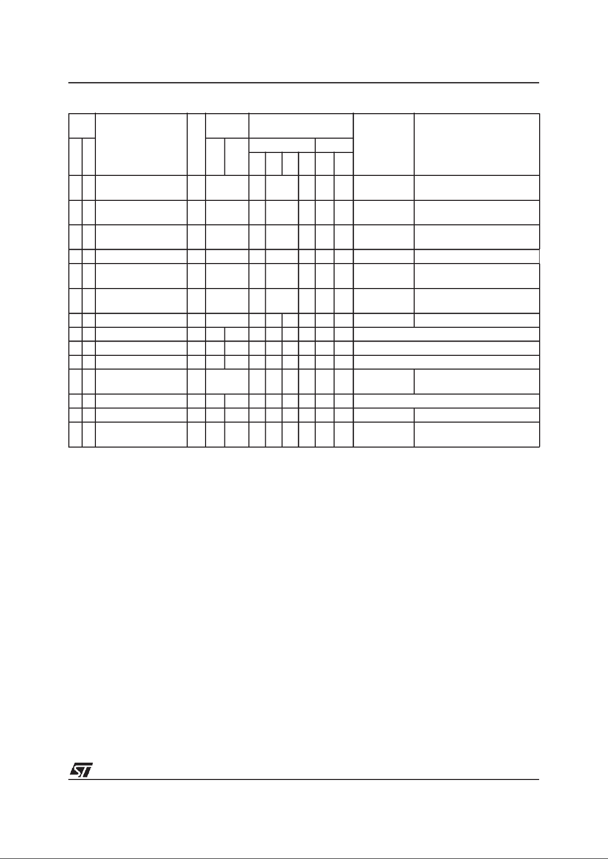
Device Summary
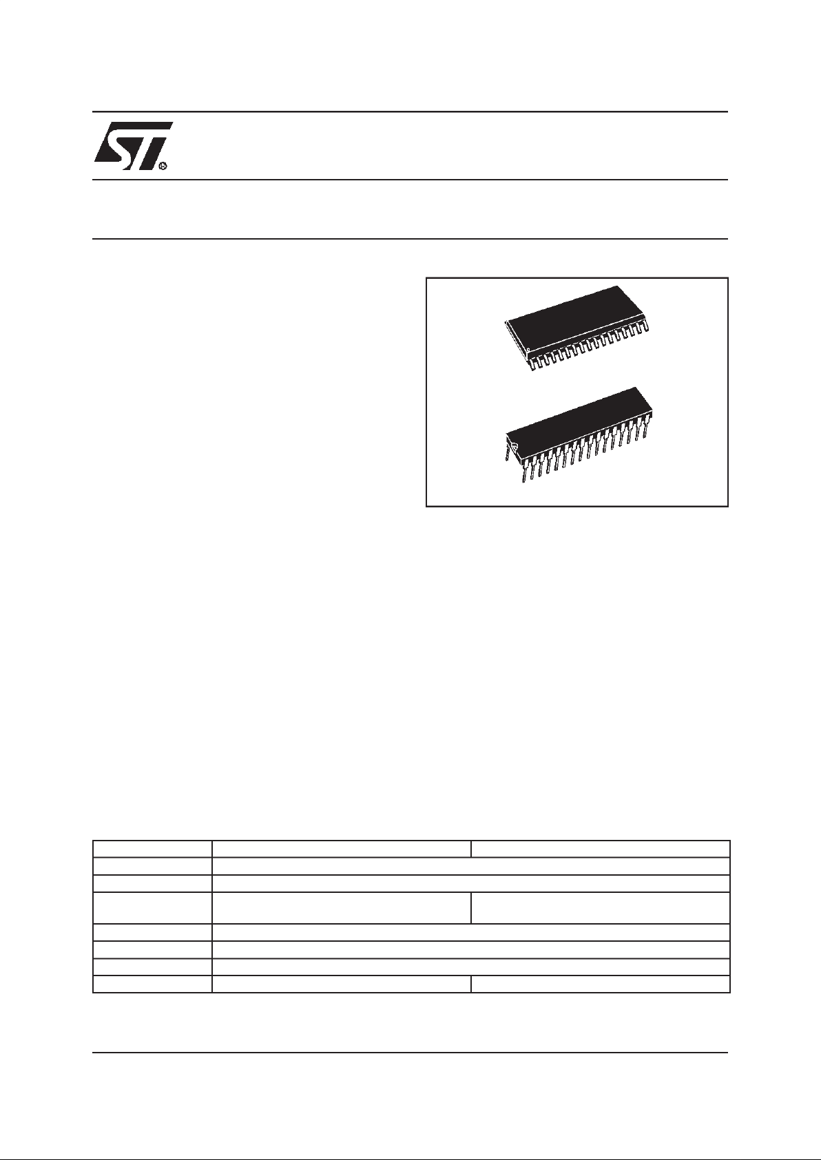
SO34
PSDIP32
Features ST72C171K2M ST72C171K2B
Flash - bytes 8K Single Voltage
RAM (stack) - bytes 256 (128)
Peripherals
2 SPGAs, 1 Op-Amp,
Watchdog, 3 Timers, SPI, SCI, ADC (11 chan.)
2 SPGAs,
Watchdog, 3 Timers, SPI, SCI, ADC (11 chan.)
Operating Supply 3.2 V to 5.5 V
CPU Frequency Up to 8 MHz (with up to 16 MHz oscillator)
Temperature Range - 40°Cto+85°C
Package SO34 PSDIP32
1
Page 2

Table of Contents
151
2/151
1
ST72C171 . . . . . . . . . . . . . . . . . . . . .......................1
1 GENERAL DESCRIPTION . . . . . . ................................................ 4
1.1 INTRODUCTION . . . . . . . . . . . . . ............................................ 4
1.2 PIN DESCRIPTION . . ..................................................... 5
1.3 MEMORY MAP . . . . . . . . . . ................................................ 8
2 FLASH PROGRAM MEMORY . . . . . . . . . . . . . . . . . ................................. 11
2.1 INTRODUCTION . . . . . . . . . . . . . ...........................................11
2.2 MAIN FEATURES . . . . . . . . . . . . . . . . . . . . . . . . . .............................. 11
2.3 STRUCTURAL ORGANISATION . . . . . . . . . . . . . . . . . . . . . . . . . . . . . . . .. . . . . . . . . . . . 11
2.4 IN-SITU PROGRAMMING (ISP) MODE . . . . . . . . . . . . . . . . . . . . . . . . . . . ...........11
2.5 MEMORY READ-OUT PROTECTION . . . . . . . . . . . . . . . . . . . . . . . . . . . . . ...........11
3 CENTRAL PROCESSING UNIT . . ............................................... 12
3.1 INTRODUCTION . . . . . . . . . . . . . ...........................................12
3.2 MAIN FEATURES . . . . . . . . . . . . . . . . . . . . . . . . . .............................. 12
3.3 CPU REGISTERS . . . .................................................... 12
4 SUPPLY, RESET AND CLOCK MANAGEMENT . . . . ................................15
4.1 MAIN FEATURES . . . . . . . . . . . . . . . . . . . . . . . . . .............................. 15
4.2 LOW VOLTAGE DETECTOR (LVD) . . . .. . . . . . . . . . ........................... 16
4.3 CLOCK SECURITY SYSTEM (CSS) . . . . . .................................... 21
4.4 CLOCK, RESET AND SUPPLY REGISTER DESCRIPTION . . . . . . . . . . . . . . . . . . . . . . 23
5 INTERRUPTS . . ............................................................. 24
5.1 NON MASKABLE SOFTWARE INTERRUPT .................................. 24
5.2 EXTERNAL INTERRUPTS . . . . . . . . . . .. . . . . . ............................... 24
5.3 PERIPHERAL INTERRUPTS ............................................... 24
6 POWER SAVING MODES . . . . . . . . . . ........................................... 27
6.1 INTRODUCTION . . . . . . . . . . . . . ...........................................27
6.2 SLOW MODE . . . . . . . .. . . . . . . . . . . . . . . . . . ................................. 27
6.3 WAIT MODE . . . . . . . . . . . . . . . . . . . . . . . . . . . . . . . . . . . . . . . . . . . . . . . . . . . ........ 28
6.4 HALT MODE . . . . . . . . . . . .. . . . . . . ........................................ 29
7 ON-CHIP PERIPHERALS . . . . . . . . . . . ...........................................30
7.1 I/O PORTS . . . .. . . . . . . . . . . . . . ...........................................30
7.2 MISCELLANEOUS REGISTERS . . . . . . . . . . . . . . . . . . . . . . . . . . . . . . . . . . . . . . . . . . . . 36
7.3 OP-AMP MODULE . ...................................................... 38
7.4 WATCHDOG TIMER (WDG) . . . . . . . . . . . . . . . . . . . . . . . . . . . . . . . . . . . . . . . . . . . . . . . 48
7.5 16-BIT TIMER . . . . . . . . . . . . . . . . . . ........................................51
7.6 PWM AUTO-RELOAD TIMER (ART) . . . . . ....................................69
7.7 SERIAL COMMUNICATIONS INTERFACE (SCI) . . . .. . . . . . . . . . . . . . . . . . . . . . . . . . . 78
7.8 SERIAL PERIPHERAL INTERFACE (SPI) . . . . . . . . . . . . . . . . . . . . . . . . . ...........89
7.9 8-BIT A/D CONVERTER (ADC) . . . . . . . . . . . . . . . . . . .......................... 102
8 INSTRUCTION SET . . . . . . . . . . . . . . . . . . .......................................106
Page 3

Table of Contents
3/151
8.1 ST7 ADDRESSING MODES . . . . . . . . . .. . . . . . .. . .. . . . . . . . . . . . . . . . . . . . . .. . . . 106
8.2 INSTRUCTION GROUPS . . . . . . . . . . . . . . . . ................................109
9 ELECTRICAL CHARACTERISTICS . . . . . . . . . . . . . . . . .............................112
9.1 PARAMETER CONDITIONS . . . . . . . . . . . ................................... 112
9.2 ABSOLUTE MAXIMUM RATINGS . . . .......................................113
9.3 OPERATING CONDITIONS . .............................................. 114
9.4 SUPPLY CURRENT CHARACTERISTICS . . . . . . . . . . . . . . . . . . . . . .............. 116
9.5 CLOCK AND TIMING CHARACTERISTICS . . . . . ............................. 119
9.6 MEMORY CHARACTERISTICS . . . . . . . . . . . . . . . . . . . . . . . . . . . . . . . . . . . . . . . . . . . 123
9.7 EMC CHARACTERISTICS . . . . . . . . . . . . . . .................................124
9.8 I/O PORT PIN CHARACTERISTICS . . . . . . . . . . . . . . . . . . . . . ................... 129
9.9 CONTROL PIN CHARACTERISTICS ....................................... 132
9.10TIMER PERIPHERAL CHARACTERISTICS .. ................................135
9.11COMMUNICATION INTERFACE CHARACTERISTICS . . . . . . . . . . . . . . . . . . . . . . . . . 136
9.128-BIT ADC CHARACTERISTICS . . . . . . . . . . . . . . . . . .......................... 139
10 GENERAL INFORMATION ................................................... 143
10.1PACKAGE MECHANICAL DATA . . . . . . . . . . . . . . . . . .......................... 143
10.2THERMAL CHARACTERISTICS . . . . . . . . . . . . . . . . . . . . .. . . . . . . . . . . . . . . . . . . . . 144
10.3SOLDERING AND GLUEABILITY INFORMATION .. . . . . . . . . . .. . . . . . ...........145
10.4PACKAGE/SOCKET FOOTPRINT PROPOSAL . . . .. . . . . . . . . . . . . . . . . . . . . . . . . . . 145
11 DEVICE CONFIGURATION AND ORDERING INFORMATION . . . . . . . . . . . .. . . . . . . . . . . 146
11.1OPTION BYTES . . ...................................................... 146
11.2DEVICE ORDERING INFORMATION . . . . ................................... 147
11.3DEVELOPMENT TOOLS . . . . . . . . . . . . . . . . . . . . . . . . .. . . . . . . . . . . . . . . . . ....... 148
11.4ST7 APPLICATION NOTES . . . . . . . .......................................149
11.5TO GET MORE INFORMATION . . . . . . . . ................................... 149
12 SUMMARY OF CHANGES . .................................................. 150
Page 4
ST72C171
4/151
1 GENERAL DESCRIPTION
1.1 INTRODUCTION
The ST72C171 is a member of the ST7 family of
Microcontrollers. All devices are based on a common industry-standard 8-bit core, featuring an enhanced instruction set.
The ST72C171 features single-voltage FLASH
memory with byte-by-byte In-Situ Programming
(ISP) capability.
Under software control, the device can be placed
in WAIT, SLOW, or HALT mode, reducing power
consumption when the application is in idle or
standby state.
The enhanced instruction set and addressing
modes of the ST7 offer bothpower andflexibility to
software developers,enabling the design of highly
efficient and compact application code. In addition
to standard 8-bitdata management, all ST7microcontrollers feature true bit manipulation, 8x8 un-
signed multiplication and indirect addressing
modes The device includes a low consumption
and fast start on-chip oscillator, CPU, Flash program memory, RAM, 22 I/O lines and the following
on-chip peripherals: Analog-to-Digital converter
(ADC) with 8 multiplexed analog inputs, Op-Amp
module, synchronous SPI serial interface, asyncronous serial interface (SCI), Watchdog timer, a
16-bit Timer featuring external Clock Input, Pulse
Generator capabilities, 2 Input Captures and 2
Output Compares, an 8-bit Timer featuring external Clock Input, Pulse Generator Capabilities (2
channels), Autoreload and Input Capture.
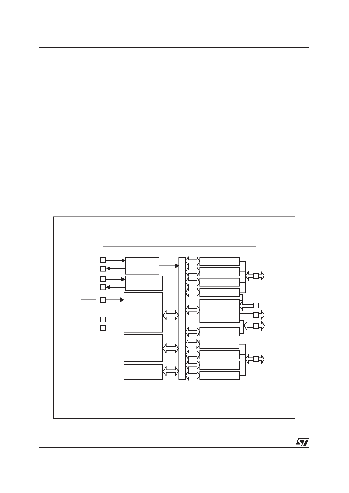
The Op-Amp module adds on-chip analog features to the MCU, that usually require using external components.
Figure 1. ST72C171 Block Diagram
ADDRESS AND DATA BUS
OSCIN
OSCOUT
RESET
16-BIT TIMER
8-BIT ADC
PORT B
WATCHDOG
Internal
CLOCK
CONTROL
256b-RAM
PA[7:0]
V
SS
V
DD
POWER
SUPPLY
8KFLASH
PORT A
PWM/ART TIMER
SPI
PB[7:0]
LVD
SCI
MULTIOSC
+
CLOCK FILTER
OP-AMP
V
SSA
V
DDA
8-BIT CORE
ALU
PORT C
PC[5:0]
OA1OUT
OA2OUT
MEMORY
OA3OUT*
*only on 34-pin devices
OA3PIN*
Page 5
ST72C171
5/151
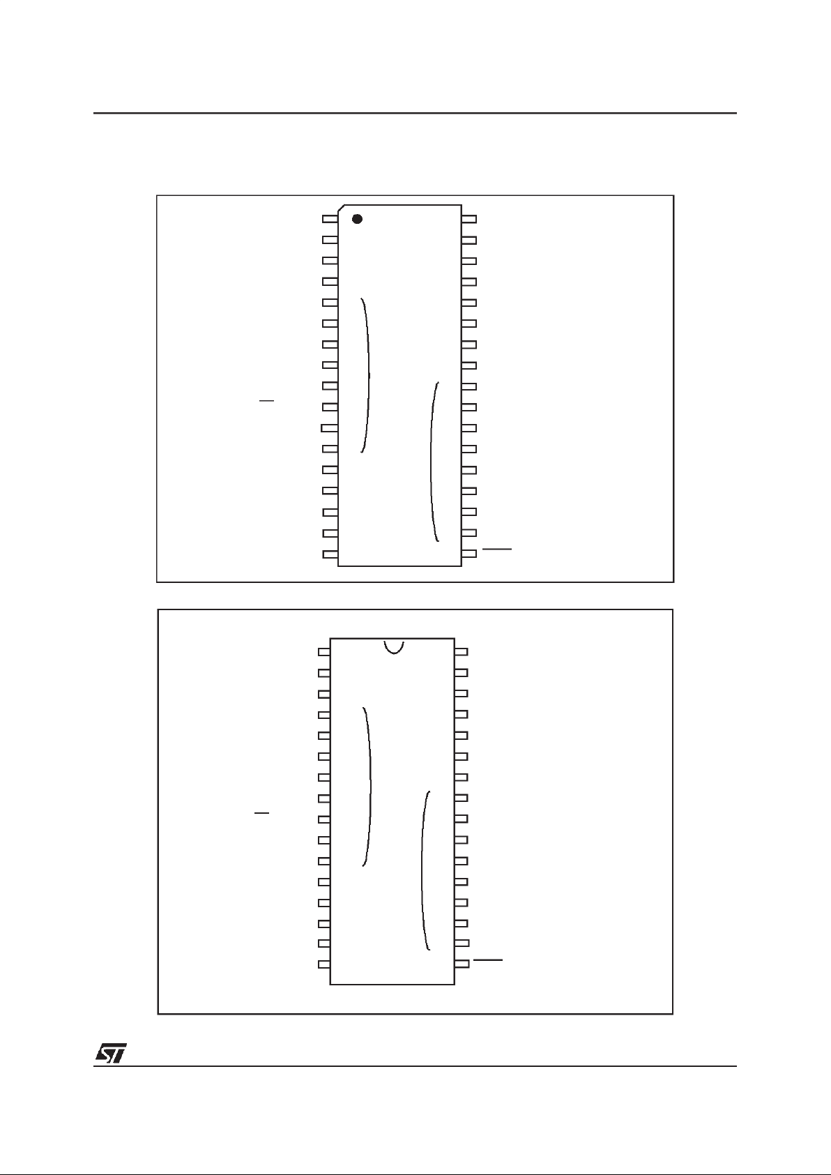
1.2 PIN DESCRIPTION
Figure 2. 34-Pin SO Package Pinout
Figure 3. 32-Pin SDIP Package Pinout
PC2 /OA1PIN / PWM0R
PC3 /OA1NIN
OA1OUT
PC4 /MCO/ OA3NIN
V
DDA
V
SSA
OA3OUT
PC5/ PWM0
PA7 / AIN7/ PWM1
PA6 / AIN6/ ARTICP0
PA5 / AIN5
PA4 / AIN4/ OCMP1
PA3 / AIN3/ OCMP2
PA2 / AIN2/ ICAP1
PA1 / AIN1/ ICAP2
PA0 / AIN0
RESET
21
22
23
24
25
26
34
33
32
31
30
29
28
27
1
2
3
4
5
6
7
8
9
10
11
12
13
14
OA2OUT
PWM1R / OA2PIN / PC1
OA2NIN / PC0
OA3PIN
TDO / PB7
RDI /PB6
ISPDATA / MISO / PB5
MOSI /
(HS)
PB4
ISPCLK / SCK /
(HS)
PB3
SS /
(HS)
PB2
ARTCLK /
(HS)
PB1
EXTCLK /
(HS)
PB0
V
DD
V
SS
OSC2
OSC1
ISPSEL
15
16
17
20
19
18
ei1
ei0
(HS)
20mA high sink capability
OA2OUT
PWM1R / OA2PIN / PC1
OA2NIN / PC0
TDO / PB7
RDI / PB6
ISPDATA / MISO / PB5
MOSI /
(HS)
PB4
ISPCLK / SCK/
(HS)
PB3
SS /
(HS)
PB2
ARTCLK /
(HS)
PB1
EXTCLK /
(HS)
PB0
V
DD
V
SS
OSC2
OSC1
ISPSEL
PC2 / OA1PIN / PWM0R
PC3 / OA1NIN
OA1OUT
PC4 / MCO
V
DDA
V
SSA
PC5 / PWM0
PA7 /AIN7 / PWM1
PA6 /AIN6 /ARTICP0
PA5 /AIN5
PA4 /AIN4 / OCMP1
PA3 /AIN3 / OCMP2
PA2 /AIN2 / ICAP1
PA1 /AIN1 / ICAP2
PA0 /AIN0
RESET
1
2
3
4
5
6
7
8
9
10
11
12
13
14
15
16
32
31
30
29
28
27
26
25
24
23
22
21
20
19
ei1
ei0
(HS)
20mA high sink capability
Page 6
ST72C171
6/151
PIN DESCRIPTION (Cont’d)
Legend / Abbreviations:
Type: I = input, O = output, S = supply
In/Output level: C = CMOS 0.3VDD/0.7VDD,
CR= CMOS Levels with resistive output (1K)
A = Analog levels
Output level: HS = high sink (on N-buffer only),
Port configuration capabilities:
– Input:float = floating, wpu = weak pull-up, int = interrupt,ana = analog
– Output: OD = open drain, T = true open drain, PP = push-pull
Note: the Reset configuration of each pin is shown in bold.
Table 1. Device Pin Description
Pin
n°
Pin Name
Type
Level Port
Main
function
(after
reset)
Alternate function
SDIP32
SO34
Input
Output
Input Output
float
wpu
int
ana
OD
PP
1 1 OA2OUT O A OA2 output
22
PC1/OA2PIN/
PWM1R
I/O C C/C
R
X X X X X Port C1
OA2 noninverting input and/or
ART PWM1 resistive output
3 3 PC0/OA2NIN I/O C/A C X X X X X Port C0 OA2 inverting input
- 4 OA3PIN I A OA3 noninverting input
4 5 PB7/TDO I/O C X ei1 X X Port B7 SCI transmit
5 6 PB6/RDI I/O C X ei1 X X Port B6 SCI receive
6 7 PB5/MISO/ISPDATA I/O C X ei1 X X Port B5
SPI data master in/slaveout or
In Situ Programming Data Input
7 8 PB4/MOSI I/O C HS X ei1 X X Port B4 SPI data master out/slave in
8 9 PB3/SCK/ISPCLK I/O C HS X ei1 X X Port B3
SPI Clock or In Situ Programming Clock Output
9 10 PB2/SS I/O C HS X ei1 X X Port B2 SPI Slave Select (active low)
10 11 PB1/ARTCLK I/O C HS X ei1 X X Port B1 ART External Clock
11 12 PB0/EXTCLK I/O C HS X ei1 X X Port B0 Timer16 External Clock
12 13 V
DD
S Digital Main Supply Voltage
13 14 V
SS
S Digital ground voltage
14 15 OSC2
Resonator oscillator inverter output or capacitor input for RC oscillator
15 16 OSC1
External clock input or Resonator oscillator inverter input or resistor input for RC oscillator
16 17 ISPSEL I C
In Situ Programming Mode Select
Must be tied to V
SS
in user mode
17 18 RESET I/O C X X External Reset
18 19 PA0/AIN0 I/O C X ei0 X X X Port A0 ADC input 0
19 20 PA1/AIN1/ICAP2 I/O C X ei0 X X X Port A1
ADC input 1 orTimer16 input
capture 2
Page 7
ST72C171
7/151
Notes:
1. In the interrupt input column, “eix” defines the associated external interrupt vector. If the weak pull-up
column (wpu) is associated with the interrupt column (int), then the I/O configuration is pull-up interrupt
input, else the configuration is floating interrupt input.
2. OSC1 andOSC2 pins connect a crystal or ceramic resonator, an external RC, or an external source to
the on-chip oscillator see dedicated See “PIN DESCRIPTION” on page 5. for more details.
20 21 PA2/AIN2/ICAP1 I/O C X ei0 X X X Port A2
ADC input 2
or Timer16 input capture 1
21 22 PA3/AIN3/OCMP2 I/O C X ei0 X X X Port A3
ADC input 3 orTimer16 output
compare 2
22 23 PA4/AIN4/OCMP1 I/O C X ei0 X X X Port A4
ADC input 4 orTimer16 output
compare 1
23 24 PA5/AIN5 I/O C X ei0 X X X Port A5 ADC input 5
24 25 PA6/AIN6/ARTICP0 I/O C X ei0 X X X Port A6
ADC input 6 or ARTinput capture
25 26 PA7/AIN7/PWM1 I/O C X ei0 X X X Port A7
ADC input 7 or ART PWM1
output
26 27 PC5/PWM0 I/O C X X X X Port C5 ART PWM0 output
- 28 OA3OUT O A OA3 output
27 29 V
SSA
Analog ground
28 30 V
DDA
Analog supply
29 31 PC4/MCO/OA3NIN I/O C X XXXPortC4
Main Clock Out or OA3 invert-
ing input
30 32 OA1OUT O A OA1 output
31 33 PC3/OA1NIN I/O C/A C X X X X Port C3 OA1 inverting input
32 34
PC2/OA1PIN/
PWM0R
I/O C/A C/C
R
X XXXPortC2
OA1 non-inverting input and/
or ART PWM0 resistive output
Pin
n°
Pin Name
Type
Level Port
Main
function
(after
reset)
Alternate function
SDIP32
SO34
Input
Output
Input Output
float
wpu
int
ana
OD
PP
Page 8
ST72C171
8/151
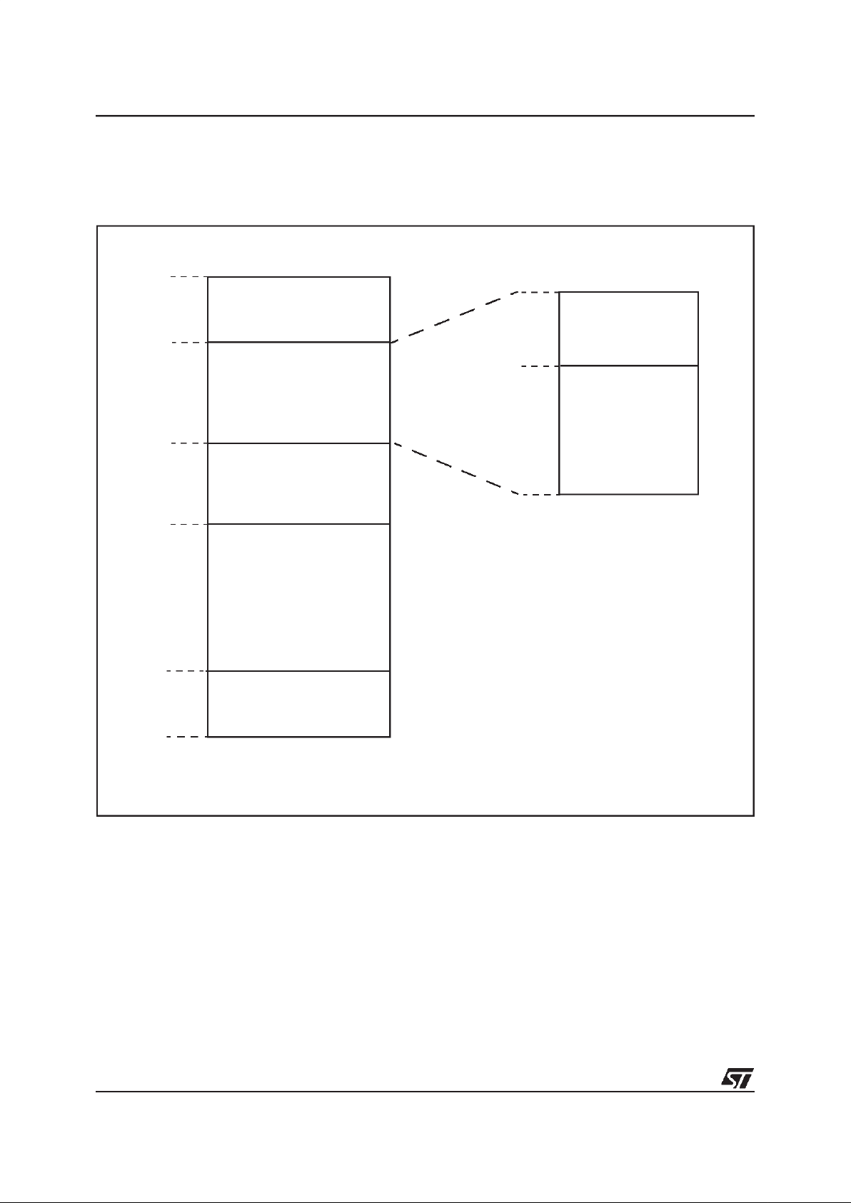
1.3 MEMORY MAP
1.3.1 Introduction
Figure 4. Program Memory Map
Short Addressing
RAM
Stack
0100h
017Fh
0080h
00FFh
0000h
8 Kbytes
Interrupt & Reset Vectors
HW Registers
017Fh
0080h
007Fh
0180h
DFFFh
Reserved
(see
Table 1.3.2)
E000h
FFDFh
FFE0h
FFFFh
(see Table 4)
256 bytes RAM
FLASH
(128 Bytes)
(128 Bytes)
Zero page
Page 9

ST72C171
9/151
1.3.2 Data Register
Table 2. Hardware Register Memory Map
Address
Block
Name
Register
Label
Register name
Reset
Status
Remarks
0000h
0001h
0002h
0003h
Port A
PADR
PADDR
PAOR
Data Register
Data Direction Register
Option Register
Not Used
00h
00h
00h
R/W
R/W
R/W
Absent
0004h
0005h
0006h
0007h
Port B
PBDR
PBDDR
PBOR
Data Register
Data Direction Register
Option Register
Not Used
00h
00h
00h
R/W
R/W
R/W
Absent
0008h
0009h
000Ah
Port C
PCDR
PCDDR
PCOR
Data Register
Data Direction Register
Option Register
00h
00h
00h
R/W
R/W
R/W
000Bh to
001Ah
Reserved Area (16 Bytes)
001Bh
001Ch
001Dh
001Eh
001Fh
OPAMP
OA1CR
OA2CR
OA3CR
OAIRR
OAVRCR
OA1 Control Register
OA2 Control Register
OA3 Control Register
OA Interrupt & Readout Register
OA Voltage Reference Control Register
00h
00h
00h
00h
00h
R/W
R/W
R/W
Section 7.3
R/W
0020h MISC1 MISCR1 Miscellaneous Register 1 00h
see
Section
4.3.5
0021h
0022h
0023h
SPI
SPIDR
SPICR
SPISR
Data I/O Register
Control Register
Status Register
xxh
0xh
00h
R/W
R/W
Read Only
0024h WDG WDGCR Watchdog Control register 7Fh R/W
0025h CRS CRSR
Clock, Reset and Supply Control / Status
Register
00h R/W
0026h to
0030h
Reserved Area (11 Bytes)
0031h
0032h
0033h
0034h0035h
0036h0037h
0038h0039h
003Ah003Bh
003Ch003Dh
003Eh003Fh
TIMER16
TACR2
TACR1
TASR
TAIC1HR
TAIC1LR
TAOC1HR
TAOC1LR
TACHR
TACLR
TAACHR
TAACLR
TAIC2HR
TAIC2LR
TAOC2HR
TAOC2LR
Control Register2
Control Register1
Status Register
Input Capture1 High Register
Input Capture1 Low Register
Output Compare1 High Register
Output Compare1 Low Register
Counter High Register
Counter Low Register
Alternate Counter High Register
Alternate Counter Low Register
Input Capture2 High Register
Input Capture2 Low Register
Output Compare2 High Register
Output Compare2 Low Register
00h
00h
xxh
xxh
xxh
80h
00h
FFh
FCh
FFh
FCh
xxh
xxh
80h
00h
R/W
R/W
Read Only
Read Only
Read Only
R/W
R/W
Read Only
Read Only
Read Only
Read Only
Read Only
Read Only
R/W
R/W
Page 10

ST72C171
10/151
0040h MISC2 MISCR2 Miscellaneous Register2 00h
see
Section
7.2.2
0041h to
004Fh
Reserved Area (15 Bytes)
0050h
0051h
0052h
0053h
0054h
SCI
SCISR
SCIDR
SCIBRR
SCICR1
SCICR2
Status Register
Data Register
Baud Rate Register
Control Register 1
Control Register 2
0C0h
0xxh
0Xxh
0xxh
00h
Read Only
R/W
R/W
R/W
R/W
0055h to
006Fh
Reserved Area (27 Bytes)
0070h
0071h
ADC
ADCDR
ADCCSR
Data Register
Control/Status Register
00h
00h
Read Only
R/W
0072h
0073h
Reserved Area (2 Bytes)
0074h
0075h
0076h
0077h
0078h
0079h
007Ah
007Bh
ART/PWM
PWMDCR1
PWMDCR0
PWMCR
ARTCSR
ARTCAR
ARTARR
ARTICCSR
ARTICR1
PWM Duty Cycle Register 1
PWM Duty Cycle Register 0
PWM Control Register
Control/Status Register
Counter Access Register
Auto Reload Register
Input Capture Control Status Register
Input Capture Register 1
00h
00h
00h
00h
00h
00h
00h
R/W
R/W
R/W
R/W
R/W
R/W
R/W
Read Only
007Ch to
007Fh
Reserved Area (4 Bytes)
Address
Block
Name
Register
Label
Register name
Reset
Status
Remarks
Page 11
ST72C171
11/151
2 FLASH PROGRAM MEMORY
2.1 INTRODUCTION
FLASH devices have a single voltage non-volatile
FLASH memory that may be programmed in-situ
(or plugged in a programming tool) on a byte-bybyte basis.
2.2 MAIN FEATURES
■ Remote In-Situ Programming (ISP) mode
■ Up to 16 bytes programmedin the same cycle
■ MTP memory (Multiple Time Programmable)
■ Read-out memory protection against piracy
2.3 STRUCTURAL ORGANISATION
The FLASH program memory is organised in a
single 8-bit wide memory block which can be used
for storing both code and data constants.
The FLASH program memory is mappedin the upper part ofthe ST7 addressing space and includes
the reset and interrupt user vector area .
2.4 IN-SITU PROGRAMMING (ISP) MODE
The FLASH program memory canbe programmed
using Remote ISP mode. This ISP mode allows
the contentsoftheST7program memory to be updated usingastandard ST7 programming tools after the device is mounted on the application board.
This feature can be implemented with a minimum
number of added components and board area impact.
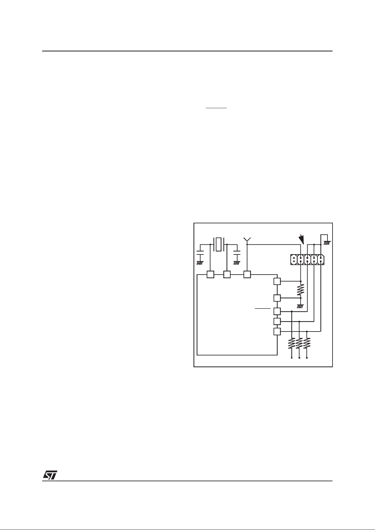
An exampleRemote ISP hardware interface to the
standard ST7 programming tool is described below. For more details on ISP programming, refer to
the ST7 Programming Specification.
Remote ISP Overview
The Remote ISP mode is initiatedby a specific sequence on the dedicated ISPSEL pin.
The Remote ISP is performedin three steps:
– Selection of the RAM execution mode
– Download of Remote ISP codein RAM
– Execution ofRemote ISP code in RAM to pro-
gram the user program into the FLASH
Remote ISP hardware configuration
In Remote ISP mode, the ST7 has to be supplied
with power (VDDand VSS) and a clock signal (oscillator and application crystal circuit for example).
This mode needs five signals (plus the VDDsignal
if necessary) to be connected to the programming
tool. This signals are:
– RESET: device reset
–VSS: device ground power supply
– ISPCLK: ISP outputserial clock pin
– ISPDATA: ISP input serial data pin
– ISPSEL: Remote ISP modeselection. Thispin
must be connected to VSSon the application
board through a pull-down resistor.
If any of thesepins areused for other purposeson
the application, a serial resistor has to be implemented to avoid a conflict ifthe other deviceforces
the signal level.
Figure 5 shows a typical hardware interface to a
standard ST7 programming tool. For more details
on the pin locations, refer to the device pinout description.
Figure 5. Typical Remote ISP Interface
2.5 MEMORY READ-OUT PROTECTION
The read-out protection is enabled through an option bit.
For FLASH devices, when this option is selected,
the program and data stored in the FLASH memory are protected against read-out piracy (including
a re-write protection). When this protection option
is removed the entire FLASH program memory is
first automatically erased. However, the E2PROM
data memory (when available) can be protected
only with ROM devices.
ISPSEL
V
SS
RESET
ISPCLK
ISPDATA
OSC1
OSC2
V
DD
ST7
HE10 CONNECTOR TYPE
TO PROGRAMMINGTOOL
10KΩ
C
L0
C
L1
APPLICATION
47KΩ
1
XTAL
Page 12
ST72C171
12/151
3 CENTRAL PROCESSING UNIT
3.1 INTRODUCTION
This CPU has a full 8-bit architecture and contains
six internal registers allowing efficient 8-bit data
manipulation.
3.2 MAIN FEATURES
■ 63 basic instructions
■ Fast 8-bit by8-bit multiply
■ 17 main addressing modes
■ Two 8-bit index registers
■ 16-bit stack pointer
■ Low power modes
■ Maskable hardware interrupts
■ Non-maskable software interrupt
3.3 CPU REGISTERS
The 6 CPU registers shown in Figure 6 are not
present in the memory mapping and are accessed
by specific instructions.
Accumulator (A)
The Accumulator is an 8-bit general purpose register used to hold operands and the results of the
arithmetic and logic calculations and to manipulate
data.
Index Registers (X and Y)
In indexed addressing modes, these 8-bitregisters
are used to create either effective addresses or
temporary storage areas for data manipulation.
(The Cross-Assembler generates a precede instruction (PRE) to indicate that the following instruction refers to the Y register.)
The Y registeris not affectedby the interrupt automatic procedures (notpushed to and popped from
the stack).
Program Counter (PC)
The program counter is a 16-bit register containing
the address of the next instruction to be executed
by the CPU. It is made of two 8-bit registers PCL
(Program Counter Low which is the LSB) andPCH
(Program CounterHigh which is the MSB).
Figure 6. CPU Registers
ACCUMULATOR
X INDEX REGISTER
Y INDEX REGISTER
STACK POINTER
CONDITION CODE REGISTER
PROGRAM COUNTER
70
1C11HI NZ
RESET VALUE = RESET VECTOR @ FFFEh-FFFFh
70
70
70
0
7
15 8
PCH
PCL
15
87 0
RESET VALUE = STACKHIGHER ADDRESS
RESET VALUE =
1X11X1XX
RESET VALUE = XXh
RESET VALUE = XXh
RESET VALUE= XXh
X = Undefined Value
Page 13

ST72C171
13/151
CPU REGISTERS (Cont’d)
CONDITION CODE REGISTER (CC)
Read/Write
Reset Value: 111x1xxx
The 8-bit Condition Code register contains the interrupt mask and four flags representative of the
result ofthe instruction just executed. This register
can also be handled by the PUSH and POP instructions.
These bits can be individually tested and/or controlled by specific instructions.
Bit 4 = H
Half carry
.
This bit is set by hardware whena carryoccursbetween bits 3 and 4 of the ALU during an ADD or
ADC instruction. It is resetby hardware during the
same instructions.
0: No half carry has occurred.
1: A half carry has occurred.
This bit is tested using the JRH or JRNH instruction. The H bit is useful in BCD arithmetic subroutines.
Bit 3 = I
Interrupt mask
.
This bit is set by hardware when entering in interrupt or by software to disable all interrupts except
the TRAP software interrupt. This bit is cleared by
software.
0: Interrupts are enabled.
1: Interrupts are disabled.
This bit is controlledby the RIM, SIM and IRET instructions and is tested by the JRM and JRNM instructions.
Note: Interrupts requested while I is set are
latched and can be processed when I is cleared.
By default an interrupt routine is not interruptable
because the I bit is set by hardware when you en-
ter it and reset by the IRET instruction at the end of
the interrupt routine. If the I bit is cleared by software in the interrupt routine, pending interruptsare
serviced regardless of the priority level of the current interrupt routine.
Bit 2 = N
Negative
.
This bit is set and cleared by hardware. It is representative of the result sign of the last arithmetic,
logical or data manipulation. It is a copy of the 7
th
bit of the result.
0:Theresultof the last operation is positive or null.
1: The result of the last operation is negative
(i.e. the most significant bit is a logic 1).
This bit isaccessed bythe JRMI andJRPL instructions.
Bit 1 = Z
Zero
.
This bit is set and cleared by hardware. Thisbit indicates that the result of the last arithmetic, logical
or data manipulation is zero.
0: The result of the last operation is different from
zero.
1: The result of the last operation is zero.
This bit is accessed by the JREQ and JRNE test
instructions.
Bit 0 = C
Carry/borrow.
This bit is set and cleared by hardware and software. It indicates an overflow or an underflow has
occurred during the last arithmetic operation.
0: No overflow or underflow has occurred.
1: An overflow or underflow hasoccurred.
This bit is driven by the SCF and RCF instructions
and tested by the JRC and JRNC instructions. It is
also affected by the “bit test and branch”, shift and
rotate instructions.
70
111HINZC
Page 14
ST72C171
14/151
CENTRAL PROCESSING UNIT (Cont’d)
Stack Pointer (SP)
Read/Write
Reset Value: 01 7Fh
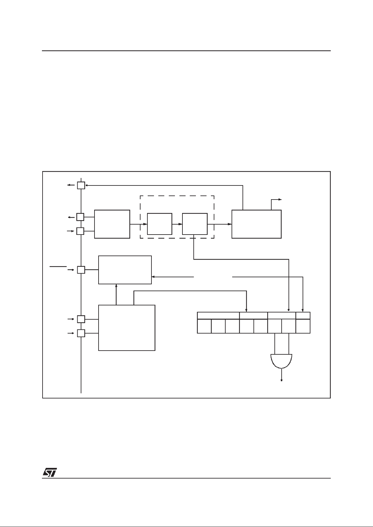
The Stack Pointer is a 16-bit register which is always pointingto the next free location in the stack.
It isthen decremented after data has been pushed
onto the stack and incremented before data is
popped from the stack (see Figure 7).
Since the stack is 128 bytes deep, the10 most significant bits are forced by hardware. Following an
MCU Reset, orafter a Reset Stack Pointer instruction (RSP),the Stack Pointer contains its reset value (the SP5 to SP0 bits are set) which is the stack
higher address.
The least significant byte of the Stack Pointer
(called S) can be directly accessed by a LD instruction.
Note: When the lower limit is exceeded, the Stack
Pointer wraps around to the stack upper limit, without indicating the stack overflow. The previously
stored information is then overwritten and therefore lost. The stack also wrapsin case of anunderflow.
The stack is used to save the return address during a subroutine call and the CPU context during
an interrupt. The user may also directly manipulate
the stack by meansof the PUSH and POP instructions. In the case of an interrupt, the PCL is stored
at the first location pointed to by the SP. Then the
other registers are stored in the next locations as
shown in Figure 7.
– When an interrupt is received, the SP is decre-
mented and the context is pushed on the stack.
– On return from interrupt, the SP is incremented
and the context is popped from thestack.
A subroutine call occupies twolocations and an interrupt five locations in the stack area.
Figure 7. Stack Manipulation Example
15 8
00000001
70
0 1 SP5 SP4 SP3 SP2 SP1 SP0
PCH
PCL
SP
PCH
PCL
SP
PCL
PCH
X
A
CC
PCH
PCL
SP
PCL
PCH
X
A
CC
PCH
PCL
SP
PCL
PCH
X
A
CC
PCH
PCL
SP
SP
Y
CALL
Subroutine
Interrupt
Event
PUSH Y POP Y IRET
RET
or RSP
@ 017Fh
@ 0100h
Stack Higher Address = 017Fh
Stack Lower Address =
0100h
Page 15
ST72C171
15/151
4 SUPPLY, RESET AND CLOCK
MANAGEMENT
The device includes a range of utility features for
securing the application in critical situations (for
example in case of a power brown-out), and reducing the number of external components. An
overview is shown in Figure 8.
4.1 Main Features
■ Supply Manager
– Main supply Low voltage detection (LVD)
– Global power down
■ Reset Sequence Manager (RSM)
■ Multi-Oscillator (MO)
– 4 Crystal/Ceramic resonator oscillators
– 2 External RC oscillators
– 1 Internal RC oscillator
■ Clock Security System (CSS)
– Clock Filter
– Backup Safe Oscillator
■ Main Clock controller (MCC)
Figure 8. Clock, Reset and Supply Block Diagram
IE SOD0- - - RF RF
CRSR
CSS- WDG
f
OSC
MAIN CLOCK
CONTROLLER
(MCC)
CF INTERRUPT
LVD
LOW VOLTAGE
DETECTOR
(LVD)
MULTI-
OSCILLATOR
(MO)
f
CPU
FROM
WATCHDOG
PERIPHERAL
MCO
OSCOUT
OSCIN
RESET
V
DD
V
SS
RESET SEQUENCE
MANAGER
(RSM)
CLOCK
FILTER
SAFE
OSC
CLOCK SECURITY SYSTEM
(CSS)
Page 16

ST72C171
16/151
4.2 LOW VOLTAGE DETECTOR (LVD)
To allow the integration of power management
features in the application, the Low Voltage Detector function (LVD) generates a static reset when
the VDDsupply voltage is below a V
IT-
reference
value. This means that it secures the power-up as
well as the power-down keeping the ST7 in reset.
The V
IT-
referencevalue fora voltage drop is lower
than the V
IT+
referencevalue forpower-on in order
to avoid a parasitic reset when theMCUstarts running and sinks current on the supply (hysteresis).
The LVD Reset circuitry generates a reset when
VDDis below:
–V
IT+
when VDDis rising
–V
IT-
when VDDis falling
The LVD function is illustrated in the Figure .
Provided the minimum VDDvalue (guaranteed for
the oscillator frequency) is above V
IT-
, the MCU
can only be in two modes:
– under full software control
– in static safe reset
In these conditions, secure operation is always ensured for the application without the need for external reset hardware.
During aLow Voltage Detector Reset, the RESET
pin is held low, thus permitting the MCU to reset
other devices.
Notes:
1. The LVD allows the device to be used without
any external RESET circuitry.
2. Three different reference levels are selectable
through the option byte according to the application requirement.
LVD application note
Application software can detect a reset caused by
the LVD by reading the LVDRF bit in the CRSR
register.
This bit is set by hardware when a LVD reset is
generated and cleared by software (writing zero).
Figure 9. Low Voltage Detector vs Reset
V
DD
V
IT+
RESET
V
IT-
V
hyst
Page 17
ST72C171
17/151
4.2.1 Reset Sequence Manager (RSM)
The RSM block of the CROSS Module includes
three RESET sources as shown in Figure 10:
■ EXTERNAL RESETSOURCE pulse
■ Internal LVD RESET (Low Voltage Detection)
■ Internal WATCHDOG RESET
These sources act on the RESET PIN and it is always kept low during the READ OPTION RESET
phase.
The RESET service routine vector is fixed at the
FFFEh-FFFFh addresses in the ST7 memory
map.
Figure 10. Reset Block Diagram
The basic RESET sequence consists of 4 phases
as shown in Figure 11:
■ OPTION BYTE reading to configure the device
■ Delay depending on the RESET source
■ 4096 cpu clock cycle delay
■ RESET vector fetch
The duration of the OPTION BYTE reading phase
(t
ROB
) is defined in the Electrical Characteristics
section. This first phase is initiated by an external
RESET pin pulse detection, a Watchdog RESET
detection, or when VDDrises up to V
LVDopt
.
The 4096 cpu clock cycledelay allows the oscillator to stabilise and to ensure thatrecovery has taken place from the Reset state.
The RESET vector fetch phase duration is 2 clock
cycles.
Figure 11. RESET Sequence Phases
f
CPU
COUNTER
RESET
R
ON
V
DD
WATCHDOG RESET
LVD RESET
INTERNAL
RESET
READ OPTION RESET
RESET
READ
OPTION BYTE
INTERNAL RESET
4096 CLOCK CYCLES
FETCH
VECTOR
DELAY
t
ROB
Page 18
ST72C171
18/151
RESET SEQUENCE MANAGER (Cont’d)
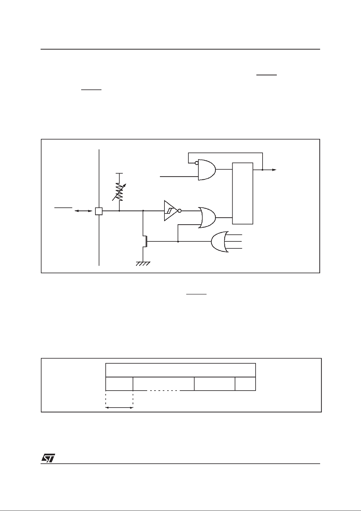
4.2.2 Asynchronous External RESET pin
The RESETpin is both an input andan open-drain
output with integrated RONweak pull-up resistor.
This pull-up has no fixed value but varies in accordance with the input voltage. It can be pulled
low by external circuitry to reset the device. See
electrical characteristics section for more details.
A RESET signal originating from an external
source must have a duration of at least t
h(RSTL)in
in
order to be recognized. This detection is asynchronous and therefore the MCU can enter reset state
even in HALT mode.
The RESET pin is an asynchronous signal which
plays a major role in EMS performance. In a noisy
environment, it is recommended to follow the
guidelines mentioned in the electrical characteristics section.
Two RESET sequences can be associated with
this RESET source: short or long external reset
pulse (see Figure 12).
Starting from the external RESET pulse recognition, the device RESET pin acts as an output that
is pulled low during at least t
w(RSTL)out
.
4.2.3 Internal Low Voltage Detection RESET
Two different RESET sequences caused by the internal LVD circuitry can be distinguished:
■ Power-On RESET
■ Voltage Drop RESET
The device RESET pin acts as an output that is
pulled low when VDD<V
IT+
(rising edge) or
VDD<V
IT-
(falling edge) as shown in Figure 12.
The LVD filters spikes on VDDlarger than t
g(VDD)
to
avoid parasitic resets.
4.2.4 Internal Watchdog RESET
The RESET sequence generated by a internal
Watchdog counter overflow is shown in Figure 12.
Starting from the Watchdog counter underflow, the
device RESET pin acts as an output that is pulled
low during at least t
w(RSTL)out
.
Figure 12. RESET Sequences
V
DD
RUN
RESET PIN
EXTERNAL
WATCHDOG
DELAY
V
IT+
V
IT-
t
h(RSTL)in
t
w(RSTL)out
RUN
DELAY
t
h(RSTL)in
DELAY
WATCHDOG UNDERFLOW
t
w(RSTL)out
RUN RUN
DELAY
RUN
RESET
RESET
SOURCE
SHORT EXT.
RESET
LVD
RESET
LONG EXT.
RESET
WATCHDOG
RESET
INTERNAL RESET (4096T
CPU
)
FETCH VECTOR
Page 19
ST72C171
19/151
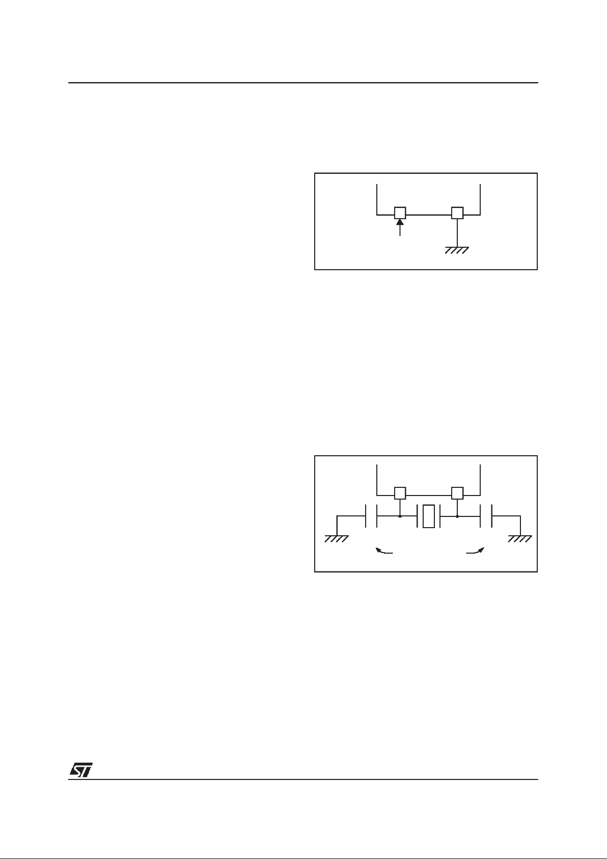
4.2.4.1 Multi-Oscillator (MO)
The Multi-Oscillator (MO) block is the main clock
supplier of the ST7. To insure an optimum integration in the application, it is based on an external
clock source and six different selectable oscillators.
The main clock of the ST7 can be generated by 8
different sources comming from the MO block:
■ an External source
■ 4 Crystal or Ceramic resonator oscillators
■ 1 External RC oscillators
■ 1 Internal High Frequency RC oscillator
Each oscillator is optimized for a given frequency
range in term of consumption and is selectable
through the Option Byte.
External Clock Source
The defaultOption Byte value selects the External
Clock in the MO block. In this mode, a clock signal
(square, sinus or triangle) with ~50% duty cycle
has to drive the OSCin pin while the OSCout pin is
tied to ground (see Figure 13).
Figure 13. MO External Clock
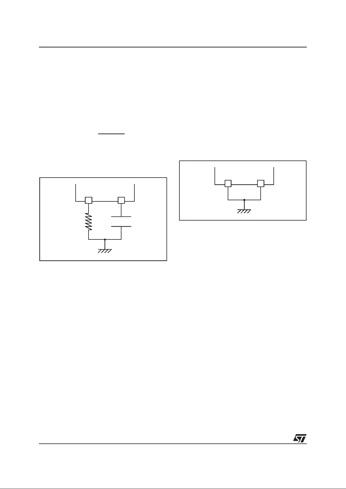
Crystal/Ceramic Oscillators
This family of oscillators allows a high accuracy on
the main clockof the ST7.The selection withinthe
list of 4 oscillators has to be done by Option Byte
according to the resonator frequency in order to
reduce the consumption. In this mode of the MO
block, the resonator and the load capacitors have
to be connected as shown in Figure 14 and have
to be mounted as close aspossible to the oscillator pins in order to minimize output distortion and
start-up stabilization time.
These oscillators, when selected via the Option
Byte, are not stopped during the RESET phase to
avoid losing time in the oscillator starting phase.
Figure 14. MO Crystal/Ceramic Resonator
OSCin OSCout
EXTERNAL
ST7
SOURCE
OSCin OSCout
LOAD
CAPACITORS
ST7
C
L1
C
L0
Page 20
ST72C171
20/151
MULTIOSCILLATOR (MO) (Cont’d)
External RC Oscillator
This oscillator allows a low cost solution on the
main clockof the ST7 using only an external resistor and an external capacitor (see Figure 15). The
selection of the external RC oscillator has to be
done by Option Byte.
The frequency of the external RCoscillator is fixed
by the resistor and the capacitor values:
The previousformula shows that in this MO mode,
the accuracy of the clock is directly linked to the
accuracy of the discrete components.
Figure 15. MO External RC
Internal RC Oscillator
The Internal RC oscillator mode is based on the
same principle as the External RC one including
the an on-chip resistor andcapacitor. This mode is
the most cost effective one with the drawback of a
lower frequency accuracy. Its frequency is in the
range of several MHz.
In this mode, the two oscillator pins have to be tied
to ground as shownin Figure 16.
The selection of the internal RC oscillator has to
be done by Option Byte.
Figure 16. MO InternalRC
f
OSC
~
N
REX.C
EX
OSCin OSCout
ST7
C
EX
R
EX
OSCin OSCout
ST7
Page 21
ST72C171
21/151
4.3 CLOCK SECURITY SYSTEM (CSS)
The Clock Security System (CSS) protects the
ST7 against main clock problems. To allow the integration of the security features in the applications, itis based on a clock filter control and anInternal safe oscillator. The CSS can be enabled or
disabled by option byte.
4.3.1 Clock Filter Control
The clock filter is based on a clock frequency limitation function.
This filter function is able to detect and filter high
frequency spikes on the ST7 main clock.
If the oscillator is not working properly (e.g. working at a harmonic frequency of the resonator), the
current active oscillator clock can be totally filtered, and then no clock signal is available for the
ST7 from this oscillator anymore. If the original
clock source recovers, the filtering is stopped automatically and the oscillator supplies the ST7
clock.
4.3.2 Safe Oscillator Control
The safe oscillator of the CSS block is a low frequency back-up clock source (see Figure 17).
If the clock signal disappears (due to a broken or
disconnected resonator...) during a safe oscillator
period, the safe oscillator delivers a low frequency
clock signalwhich allows the ST7 to perform some
rescue operations.
Automatically, theST7 clock sourceswitches back
from the safe oscillator if the original clock source
recovers.
Limitation detection
The automatic safe oscillator selection is notified
by hardware setting the CSSD bit of the CRSR
register. An interrupt can be generated if the CSSIE bit has been previously set.
These two bits are described in the CRSR register
description.
4.3.3 Low Power Modes
4.3.4 Interrupts
The CSS interrupt event generates an interrupt if
the corresponding Enable Control Bit (CSSIE) is
set and the interrupt mask in the CC register is reset (RIM instruction).
Figure 17. Clock Filter Function and Safe Oscillator Function
Mode Description
WAIT
No effect on CSS. CSS interrupt cause the
device to exit from Wait mode.
HALT
The CRSR register is frozen. The CSS (including the safe oscillator) is disabled until
HALT mode is exited.The previous CSS
configuration resumes when the MCU is
woken up by aninterrupt with “exit from
HALT mode” capability or from the counter
reset value when the MCU is woken up by a
RESET.
Interrupt Event
Event
Flag
Enable
Control
Bit
Exit
from
Wait
Exit
from
Halt
CSS event detection
(safe oscillator activated as main clock)
CSSD CSSIE Yes No
f
OSC
/2
f
CPU
f
OSC
/2
f
CPU
f
SFOSC
SAFE OSCILLATOR
FUNCTION
CLOCK FILTER
FUNCTION
Page 22
ST72C171
22/151
4.3.5 Main Clock Controller (MCC)
The MCC block supplies the clock for the ST7
CPU anditsinternal peripherals. It allows the power saving modes such as SLOW mode to be managed by the application.
All functions are managed by the Miscellaneous
Register 1 (MISCR1).
The MCC block consists of:
– a programmable CPU clock prescaler
– a clock-out signalto supply external devices
The prescaler allows the selection of the main
clock frequency and is controlled with three bits of
the MISCR1: CP1, CP0 and SMS.
The clock-out capability is anAlternate Function of
an I/O port pin, providing the f
CPU
clock as an output for driving external devices. It is controlled by
the MCO bit in the MISCR1 register.
Figure 18. Main Clock Controller (MCC) Block Diagram
DIV 2, 4, 8, 16
DIV 2
SMSCP1 CP0
CPU CLOCK
MISCR1
TO CPU AND
PERIPHERALS
f
OSC
MCO
PORT
FUNCTION
ALTERNATE
OSCOUT
OSCIN
MULTI-
OSCILLATOR
(MO)
CLOCK
FILTER
(CF)
MCO
f
CPU
Page 23
ST72C171
23/151
4.4 CLOCK, RESET AND SUPPLY REGISTER DESCRIPTION
CLOCK RESET AND SUPPLY REGISTER
(CRSR)
Read/Write
Reset Value: 000x 000x (00h)
Bit 7:5 = Reserved.
Bit 4 = LVDRF
LVD Reset Flag
This bit indicates when set that the last Reset was
generated by the LVD block. It is set by hardware
(LVD reset) and cleared by software (writing zero)
or a Watchdog Reset. See WDGRF flag description for more details.
Bit 3 = Reserved.
Bit 2 = CSSIE
CSS Interrupt Enable
This bit allows to enable the interrupt when a distrurbance is detected by the Clock Security System (CSSD bit set). It is set and cleared by software.
0: Clock Filter interrupt disable
1: Clock Filter interrupt enable
Bit 1 = CSSD
CSS Safe Osc. Detection
This bit indicates that the safe oscillator of the CSS
block has been selected. It is set by hardware and
cleared by reading the CRSR register when the
original oscillator recovers.
0: Safe oscillator is not active
1: Safe oscillator has been activated
Bit 0 = WDGRF
WatchDog Reset Flag
This bit indicates when set that the last Reset was
generated by the Watchdog peripheral. It isset by
hardware (watchdog reset) and cleared by software (writing zero) or an LVD Reset.
Combined with the LVDRF flag information, the
flag description is given by the following table.
Table 3. Supply, Reset and Clock Register Map and Reset Values
70
---
LVD
RF
-
CSSIECSSDWDG
RF
RESET Sources LVDRF WDGRF
External RESET pin 0 0
Watchdog 0 1
LVD 1 X
Address
(Hex.)
Register
Label
76543210
0020h
MISCR
Reset Value
PEI3
0
PEI2
0
MCO
0
PEI1
0
PEI0
0
CP1
0
CP0
0
SMS
0
0025h
CRSR
Reset Value
-
0
-
0
-
0
LVDRF
x
-
0
CSSIE0CSSD0WDGRF
x
Page 24

ST72C171
24/151
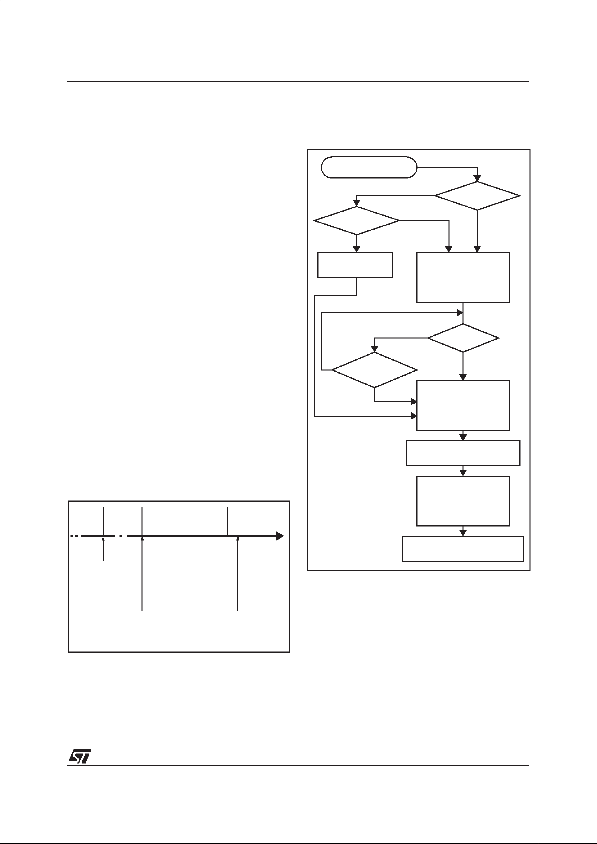
5 INTERRUPTS
The ST7 core may be interruptedby one oftwo different methods: maskable hardware interrupts as
listed in the Interrupt Mapping Table and a nonmaskable software interrupt (TRAP). The Interrupt
processing flowchart is shown in Figure 19.
The maskableinterrupts must be enabled clearing
the I bit in order to be serviced. However, disabled
interrupts may be latched and processed when
they are enabled (see external interrupts subsection).
When an interrupt has to be serviced:
– Normal processing is suspended at the end of
the current instruction execution.
– The PC, X, A and CC registers are saved onto
the stack.
– The I bit of the CC register is set to prevent addi-
tional interrupts.
– ThePC isthenloaded with the interrupt vectorof
the interruptto service and the first instruction of
the interrupt service routine is fetched (refer to
the Interrupt Mapping Tablefor vector addresses).
The interrupt service routine should finish with the
IRET instruction which causes the contents of the
saved registers to be recovered from thestack.
Note: As a consequence of the IRET instruction,
the I bit will be cleared and the main program will
resume.
Priority management
By default, a servicing interrupt cannot be interrupted because the I bit is set by hardware entering in interrupt routine.
In the case when several interrupts are simultaneously pending, an hardware priority defines which
one will be serviced first (see the Interrupt Mapping Table).
Interrupts and Low power mode
All interrupts allow the processor to leave the
WAIT low power mode. Only external and specifically mentioned interrupts allow the processor to
leave the HALT low power mode (refer to the “Exit
from HALT“ column in the Interrupt Mapping Table).
5.1 NON MASKABLE SOFTWARE INTERRUPT
This interrupt is entered when the TRAP instruction is executed regardless of the stateof theI bit.
It will be serviced according to the flowchart on
Figure 19.
5.2 EXTERNAL INTERRUPTS
External interrupt vectors can be loaded into the
PC register if the corresponding external interrupt
occurred and if the I bit is cleared. Theseinterrupts
allow the processor to leave the Halt low power
mode.
The external interrupt polarity is selected through
the miscellaneous register or interrupt register (if
available).
An external interrupt triggered on edge will be
latched and the interrupt request automatically
cleared upon entering the interrupt serviceroutine.
If several input pins, connected to the same interrupt vector, are configured as interrupts, their signals are logically ANDed before entering the edge/
level detection block.
Caution:The type of sensitivitydefinedin the Miscellaneous or Interrupt register (if available) applies to the ei source. In case of an ANDedsource
(as described on the I/O ports section), a low level
on an I/O pin configured as input with interrupt,
masks the interrupt requesteven in case of risingedge sensitivity.
5.3 PERIPHERAL INTERRUPTS
Different peripheral interrupt flags in the status
register are able to cause an interrupt when they
are active if both:
– The I bit of the CC register is cleared.
– Thecorresponding enable bit is setin thecontrol
register.
If any of these two conditions is false, the interrupt
is latched and thus remains pending.
Clearing an interrupt request is done by:
– Writing “0”to the corresponding bit in the status
register or
– Access tothe status registerwhile the flag isset
followed by a read or write of an associated register.
Note: the clearing sequence resets the internal
latch. A pending interrupt (i.e. waiting for being enabled) will therefore be lost ifthe clear sequence is
executed.
Page 25

ST72C171
25/151
INTERRUPTS (Cont’d)
Figure 19. Interrupt Processing Flowchart
I BIT SET?
Y
N
IRET?
Y
N
FROM RESET
LOAD PC FROM INTERRUPT VECTOR
STACK PC, X, A, CC
SET I BIT
FETCH NEXT INSTRUCTION
EXECUTEINSTRUCTION
THIS CLEARS I BIT BY DEFAULT
RESTORE PC,X, A,CC FROM STACK
INTERRUPT
Y
N
PENDING?
Page 26

ST72C171
26/151
INTERRUPTS (Cont’d)
Table 4. Interrupt Mapping
Source
Block
Description
Register
Label
Flag
Exit from
HALT
Vector
Address
Priority
Order
RESET Reset N/A N/A yes FFFEh-FFFFh
TRAP Software N/A N/A no FFFCh-FFFDh
ei0 Ext. Interrupt ei0 N/A N/A yes FFFAh-FFFBh
ei1 Ext. Interrupt ei1 N/A N/A yes FFF8h-FFF9h
CSS Clock Filter Interrupt CRSR CSSD no FFF6h-FFF7h
SPI
Transfer Complete
SPISR
SPIF
no FFF4h-FFF5h
Mode Fault MODF
TIMER 16
Input Capture 1
TASR
ICF1_1
no FFF2h-FFF3h
Output Compare 1 OCF1_1
Input Capture 2 ICF2_1
Output Compare 2 OCF2_1
Timer Overflow TOF_1
ART/PWM
Input Capture 1 ARTICCSR ICF0
yes
FFF0h-FFF1h
Timer Overflow ARTCSR OVF FFEEh-FFEFh
OP-AMP
OA1 Interrupt
OIRR
OA1V
yes
FFECh-FFEDh
OA2 Interrupt OA2V FFEAh-FFEBh
NOT USED FFE6-FFE9
SCI SCI Peripheral Interrupts no FFE4-FFE5
NOT USED FFE0h-FFE3h
Highest
Priority
Priority
Lowest
Page 27
ST72C171
27/151
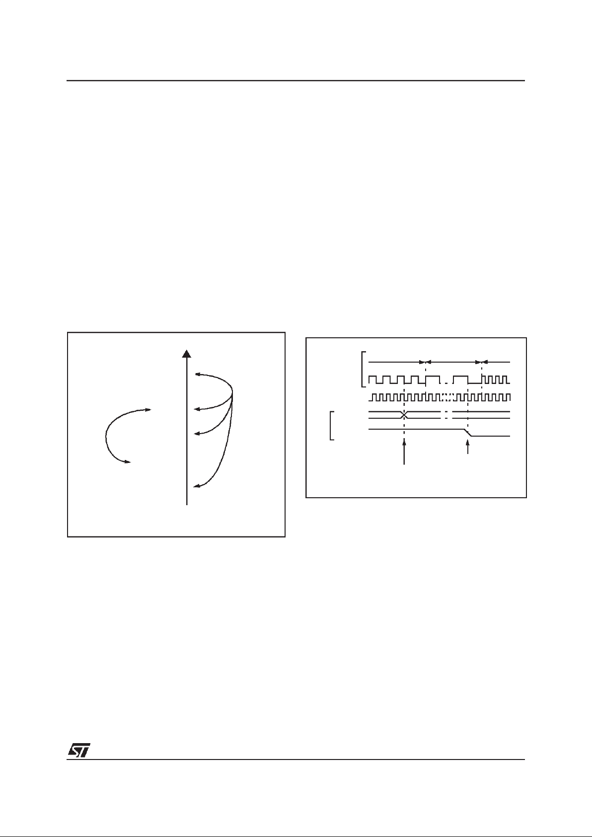
6 POWER SAVING MODES
6.1 INTRODUCTION
To give a large measure of flexibilitytotheapplication in terms of power consumption, three main
power saving modes are implemented in the ST7
(see Figure 20).
After a RESET the normal operating mode is selected by default (RUN mode). This mode drives
the device (CPU and embedded peripherals) by
means of a master clock which is based on the
main oscillator frequency divided by 2 (f
CPU
).
From Run mode, the different power saving
modes may be selected by setting the relevant
register bits or by calling the specific ST7 software
instruction whose action depends on the the oscillator status.
Figure 20. Power Saving Mode Transitions
6.2 SLOW MODE
This mode has two targets:
– To reduce powerconsumption bydecreasingthe
internal clock in the device,
– To adapt the internal clock frequency (f
CPU
)to
the available supply voltage.
SLOW mode is controlled by three bits in the
MISCR1 register: the SMS bit which enables or
disables Slow modeand two CPx bits which select
the internal slow frequency (f
CPU
).
In this mode, the oscillator frequency can bedivided by 4, 8, 16 or 32 instead of 2 in normal operating mode. The CPU and peripherals are clocked at
this lower frequency.
Note: SLOW-WAIT mode is activated when enterring the WAIT mode while the device is already in
SLOW mode.
Figure 21. SLOW Mode Clock Transitions
POWER CONSUMPTION
WAIT
SLOW
RUN
HALT
High
Low
SLOW WAIT
00 01
SMS
CP1:0
f
CPU
NEW SLOW
NORMAL RUN MODE
MISCR1
FREQUENCY
REQUEST
REQUEST
f
OSC
/2
f
OSC
/4 f
OSC
/8 f
OSC
/2
Page 28

ST72C171
28/151
POWER SAVING MODES (Cont’d)
6.3 WAIT MODE
WAIT mode places the MCU in a low power consumption mode by stopping the CPU.
This power saving mode is selectedby calling the
“WFI” ST7 software instruction.
All peripherals remain active. During WAIT mode,
the I bit of the CC register are forced to 0, to enable all interrupts. All other registers and memory
remain unchanged. The MCU remains in WAIT
mode until an interrupt or Reset occurs, whereupon the Program Counter branches to the starting
address of the interrupt or Reset serviceroutine.
The MCU will remain in WAIT mode until a Reset
or an Interrupt occurs, causing it to wake up.
Refer to Figure22.
Figure 22. WAIT Mode Flow-chart
Note: Before servicing an interrupt, the CC regis-
ter is pushed on the stack. The Ibit of the CC register is set during the interrupt routine and cleared
when the CC register is popped.
WFI INSTRUCTION
RESET
INTERRUPT
Y
N
N
Y
CPU
OSCILLATOR
PERIPHERALS
IBIT
ON
ON
0
OFF
FETCH RESET VECTOR
OR SERVICE INTERRUPT
CPU
OSCILLATOR
PERIPHERALS
IBIT
ON
OFF
1
ON
CPU
OSCILLATOR
PERIPHERALS
I BIT(see note)
ON
ON
1
ON
4096 CPU CLOCK CYCLE
DELAY
Page 29
ST72C171
29/151
POWER SAVING MODES (Cont’d)
6.4 HALT MODE
The HALT mode is the lowest power consumption
mode of the MCU. It is entered by executing the
ST7 HALT instruction (see Figure 24).
The MCU can exit HALT mode on reception of either an specific interrupt (see Table 4, “Interrupt
Mapping,” on page 26) or a RESET. When exiting
HALT mode by means of a RESET or an interrupt,
the oscillator is immediately turned on and the
4096 CPU cycle delay is used to stabilize the oscillator. After the start up delay, the CPU resumes
operation by servicing the interrupt or by fetching
the reset vector which woke it up (see Figure 23).
When entering HALT mode, the I bit in the CC register is forced to 0 to enable interrupts. Therefore,
if an interrupt is pending, the MCU wakes immediately.
In the HALT mode the main oscillator is turned off
causing all internal processing to be stopped, including the operation of the on-chip peripherals.
All peripherals are not clocked except the ones
which get their clock supply from another clock
generator (such as an external or auxiliary oscillator).
The compatibility of Watchdog operation with
HALT mode is configured by the “WDGHALT” option bit of the option byte. The HALT instruction
when executed while the Watchdog system is enabled, can generate a Watchdog RESET (see
Section 11.1 OPTION BYTES for more details).
Figure 23. HALT Mode Timing Overview
Figure 24. HALT Mode Flow-chart
Notes:
1. WDGHALTis anoption bit. See option byte sec-
tion for more details.
2. Peripheral clocked with an external clock source
can still be active.
3. Only some specific interrupts can exit the MCU
from HALT mode (such as external interrupt). Refer to Table 4, “Interrupt Mapping,” on page 26 for
more details.
4. Before servicing an interrupt, the CC register is
pushed on the stack. The I bit of the CCregister is
set during the interrupt routine and cleared when
the CC register is popped.
HALTRUN RUN
4096 CPU CYCLE
DELAY
RESET
OR
INTERRUPT
HALT
INSTRUCTION
FETCH
VECTOR
HALT INSTRUCTION
RESET
INTERRUPT
3)
Y
N
N
Y
CPU
OSCILLATOR
PERIPHERALS
2)
IBIT
OFF
OFF
0
OFF
FETCH RESET VECTOR
OR SERVICE INTERRUPT
CPU
OSCILLATOR
PERIPHERALS
IBIT
ON
OFF
1
ON
CPU
OSCILLATOR
PERIPHERALS
IBIT
4)
ON
ON
1
ON
4096 CPU CLOCK CYCLE
DELAY
WATCHDOG
ENABLE
DISABLE
WDGHALT
1)
0
WATCHDOG
RESET
1
Page 30

ST72C171
30/151
7 ON-CHIP PERIPHERALS
7.1 I/O PORTS
7.1.1 Introduction
The I/O ports offer different functional modes:
– transferof datathrough digital inputsandoutputs
and for specific pins:
– analog signal input (ADC)
– alternate signal input/output for the on-chip pe-
ripherals.
– external interrupt generation
An I/O port is composed of up to 8 pins. Each pin
can be programmed independently as digital input
(with or without interrupt generation) or digital output.
7.1.2 Functional Description
Each port is associated to 2 mainregisters:
– Data Register (DR)
– Data Direction Register (DDR)
and some of them to an optional register (see reg-
ister description):
– Option Register (OR)
Each I/Opin may be programmed using thecorre-
sponding registerbits in DDR and ORregisters:bit
X corresponding topinXof the port. The samecorrespondence is used for the DR register.
The following description takes into account the
OR register, for specific ports whichdo notprovide
this register refer to the I/O Port Implementation
Section 7.1.2.5. The generic I/O block diagram is
shown on Figure 26.
7.1.2.1 Input Modes
The input configuration is selected by clearing the
corresponding DDR register bit.
In this case, reading the DR register returns the
digital value applied to the external I/O pin.
Different input modes can beselected bysoftware
through the OR register.
Notes:
1. All the inputs are triggered by a Schmitt trigger.
2. When switching from input mode to output
mode, the DR register should be written first to
output the correct value as soon as the port isconfigured as an output.
Interrupt function
When an I/O is configured in Input with Interrupt,
an event on this I/O can generate an external Interrupt request to the CPU. The interrupt sensitivity is given independently according to the description mentioned in the Miscellaneous register or in
the interrupt register (where available).
Each pin can independently generate an Interrupt
request.
Each external interrupt vector is linked to a dedicated group of I/O port pins (see Interrupts section). If more than one input pin is selected simultaneously as interrupt source, this is logically
ORed. For this reason if one of the interrupt pins is
tied low, it masks the other ones.
7.1.2.2 Output Mode
The pin is configured inoutput mode by setting the
corresponding DDR register bit.
In this mode, writing “0” or “1” to the DR register
applies this digital value to the I/O pin through the
latch. Then reading the DR register returns the
previously stored value.
Note: In this mode, the interrupt function is disabled.
7.1.2.3 Digital Alternate Function
When an on-chip peripheral is configured to use a
pin, the alternate function is automatically selected. This alternate function takes priority over
standard I/O programming. When the signal is
coming from an on-chip peripheral, the I/O pin is
automatically configured in outputmode (push-pull
or open drain according to the peripheral).
When the signal is going to an on-chip peripheral,
the I/O pin has to be configured in input mode. In
this case, the pin’s state is also digitally readable
by addressing the DR register.
Notes:
1. Input pull-up configuration can cause an unexpected value at the input of the alternate peripheral input.
2. When the on-chip peripheral uses a pin asinput
and output, this pinmust beconfigured as an input
(DDR = 0).
Warning
: The alternate function must not beacti-
vated as long as the pin is configured as input with
interrupt, in order to avoid generating spurious interrupts.
Page 31

ST72C171
31/151
I/O PORTS (Cont’d)
7.1.2.4 Analog Alternate Function
When the pin is used as an ADC input theI/O must
be configured as input, floating. The analog multiplexer (controlled by the ADC registers) switches
the analog voltage present on the selected pin to
the common analog rail which is connected to the
ADC input.
It is recommended not to change the voltage level
or loading on any port pin while conversion is in
progress. Furthermore it is recommended not to
have clocking pins located close to a selected analog pin.
Warning
: The analog input voltage level must be
within the limits stated in the Absolute Maximum
Ratings.
7.1.2.5 I/O Port Implementation
The hardware implementation on each I/O port depends on the settings in the DDR and OR registers
and specific feature of the I/O port such as ADCInput (see Figure 26) or true open drain. Switching
these I/O ports from one state to another should
be done in a sequence that prevents unwanted
side effects. Recommended safe transitions are illustrated in Figure 25. Other transitions are potentially risky and should be avoided, since they are
likely to present unwanted side-effects such as
spurious interrupt generation.
Figure 25. Recommended I/O StateTransition Diagram
with interrupt
INPUT
OUTPUT
no interrupt
INPUT
push-pullopen-drain
OUTPUT
Page 32

ST72C171
32/151
I/O PORTS (Cont’d)
Figure 26. I/O Block Diagram
Table 5. Port Mode Configuration
Legend:
0 - present, not activated
1 - present and activated
Notes:
– No OR Register on some ports (see register map).
– ADC Switch on ports with analog alternate functions.
DR
DDR
LATCH
LATCH
DATA BUS
DR SEL
DDR SEL
V
DD
PAD
ANALOG
SWITCH
ANALOG ENABLE
(ADC)
M
U
X
ALTERNATE
ALTERNATE
ALTERNATE ENABLE
COMMON ANALOG RAIL
ALTERNATE
M
U
X
ALTERNATE INPUT
PULL-UP(S
EE TABLE BELOW)
OUTPUT
P-BUFFER
(S
EE TABLE BELOW)
N-BUFFER
1
0
1
0
OR
LATCH
ORSEL
FROM
OTHER
BITS
EXTERNAL
PULL-UP
CONDITION
ENABLE
ENABLE
GND
(S
EE TABLE BELOW)
(S
EE NOTE BELOW)
CMOS
SCHMITT TRIGGER
SOURCE (EIx)
INTERRUPT
SENSITIVITY
SEL
Configuration Mode Pull-up P-buffer
Floating 0 0
Pull-up 1 0
Push-pull 0 1
True Open Drain not present not present
Open Drain (logic level) 0 0
Page 33

ST72C171
33/151
I/O PORTS (Cont’d)
7.1.2.6 Device Specific Configurations
Table 6. Port Configuration
*Reset state.
Port Pin name
Input(DDR =0) Output (DDR=1)
OR = 0 OR = 1 OR = 0 OR = 1
Port A PA7: PA0 floating* pull-up with interrupt open drain push-pull
Port B
PB0:PB4 floating* pull-up with interrupt
open drain
high sink capability
push-pull
PB5:PB7 floating* pull-up with interrupt open drain push-pull
Port C PC0:PC5 floating* pull-up open drain push-pull
Page 34

ST72C171
34/151
I/O PORTS (Cont’d)
7.1.3 Register Description
DATA REGISTERS
Port A Data Register (PADR)
Port B Data Register (PBDR)
Port C DataRegister (PCDR)
Read/Write
Reset Value: 0000 0000 (00h)
Bit 7:0 = D[7:0]
Data Register 8 bits.
The DR register has a specific behaviour according to the selectedinput/output configuration. Writing the DR register is always taken in account
even if the pin is configured as an input. Reading
the DRregisterreturns either theDR register latch
content (pin configured as output) or the digital value applied to the I/O pin (pin configured as input).
DATA DIRECTION REGISTERS
Port A Data Direction Register (PADDR)
Port B Data Direction Register (PBDDR)
Port C DataDirection Register (PCDDR)
Read/Write
Reset Value: 0000 0000 (00h) (input mode)
Bit 7:0 = DD[7:0]
Data Direction Register 8 bits.
The DDR register gives the input/output direction
configuration of the pins. Each bits is set and
cleared by software.
0: Input mode
1: Output mode
OPTION REGISTERS
PORT A Option Register (PAOR)
PORT B Option Register (PBOR)
PORT C Option Register (PCOR)
Read/Write
Reset Value: 0000 0000 (00h) (no interrupt)
Bit 7:0 = O[7:0]
Option Register 8 bits.
The PAOR, PBOR and PCOR registers are used
to select pull-up or floating configuration in input
mode.
Each bit is set and cleared by software.
Input mode:
0: Floating input
1: Input pull-up (with or without interrupt see Table
6)
70
D7 D6 D5 D4 D3 D2 D1 D0
70
DD7 DD6 DD5 DD4 DD3 DD2 DD1 DD0
70
O7 O6 O5 O4 O3 O2 O1 O0
Page 35

ST72C171
35/151
I/O PORTS (Cont’d)
Table 7. I/O Port Register Map andReset Values
Address
(Hex.)
Register
Label
76543210
0000h
PADR
Reset Value
D7
0
D6
0
D5
0
D4
0
D3
0
D2
0
D1
0
D0
0
0001h
PADDR
Reset Value
D7
0
D6
0
D5
0
DD4
0
DD3
0
DD2
0
DD1
0
DD0
0
0002h
PAOR
Reset Value
D7
0
D6
0
D5
0
O4
0
O3
0
O2
0
O1
0
O0
0
0004h
PBDR
Reset Value
D7
0
D6
0
D5
0
D4
0
D3
0
D2
0
D1
0
D0
0
0005h
PBDDR
Reset Value
DD7
0
DD6
0
DD5
0
DD4
0
DD3
0
DD2
0
DD1
0
DD0
0
0006h
PBOR
Reset Value
O7
0
O6
0
O5
0
O4
0
O3
0
O2
0
O1
0
O0
0
0008h
PCDR
Reset Value
D7
0
D6
0
D5
0
D4
0
D3
0
D2
0
D1
0
D0
0
0009h
PCDDR
Reset Value
DD7
0
DD6
0
DD5
0
DD4
0
DD3
0
DD2
0
DD1
0
DD0
0
000Ah
PCOR
Reset Value
O7
0
O6
0
O5
0
O4
0
O3
0
O2
0
O1
0
O0
0
Page 36

ST72C171
36/151
7.2 MISCELLANEOUS REGISTERS
7.2.1 Miscellaneous Register 1 (MISCR1)
Miscellaneous register 1 isused select SLOW operating mode.Bits 3, 4, 6, and 7 determine the polarity of external interrupt requests.
Register Address: 0020h — Read/Write
Reset Value: 0000 0000 (00h)
Bit 7:6 = PEI[3:2]
Polarity Options of External In-
terrupt ei1. (Port B)
.
These bits are set and cleared by software. These
bits determine which event causes the external interrupt (ei1) on port B according to Table 8.
Table 8. ei1Ext. Int. Polarity Options
Bit 5 = MCO
Main clock out selection
This bit enablesthe MCO alternatefunction on the
I/O port. It is set and cleared by software.
0: MCO alternate function disabled
(I/O pin free for general-purpose I/O)
1: MCO alternate function enabled
(f
OSC
/2 on I/O port)
This bit is set and cleared by software. When set it
can beused to output the internal clock to the dedicated I/O port.
Bit 4:3 = PEI[1:0]
Polarity Options of External In-
terrupt ei0. (Port A)
These bits determine which event causes the external interrupt (ei0) on port A according to Table
9.
Table 9. ei0 Ext. Int. Polarity Options
Bit 2:1 = CP[1:0]
CPU clock prescaler
These bits are set and cleared by software. They
determine the CPU clock when the SMS bit is set
according to the following table.
Table 10. f
CPU
Value in Slow Mode
Bit 0 = SMS
Slow Mode Select
This bit is set andcleared by software.
0: Normal Mode - f
CPU=fOSC
/2
1: Slow Mode-the f
CPU
valueis determinedbythe
PC[1:0] bits.
70
PEI3 PEI2 MCO PEI1 PEI0 CP1 CP0 SMS
MODE PEI3 PEI2
Falling edge and low level
(Reset state)
00
Rising edge only 0 1
Falling edge only 1 0
Rising and falling edge 1 1
MODE PEI1 PEI0
Falling edge and low level
(Reset state)
00
Rising edge only 0 1
Falling edge only 1 0
Rising and falling edge 1 1
f
CPU
Value CP1 CP0
f
OSC
/4 0 0
f
OSC
/8 1 0
f
OSC
/16 0 1
f
OSC
/32 1 1
Page 37

ST72C171
37/151
7.2.2 Miscellaneous Register 2 (MISCR2)
Miscellaneous register 2 is used to configure of
SPI and the output selection of thePWMs.
Register Address: 0040h — Read/Write
Reset Value: 0000 0000 (00h)
Bit 7:5 = not used
Bit 4 = SPIOD
SPI output disable
This bit isusedto disable the SPI output onthe I/O
port (in both master or slave mode).
0: SPI output enabled
1: SPI output disabled
(I/O pin free for general-purpose I/O)
Bit 3 = P1OS
PWM1 output select
This bit is used to select the output for the PWM1
channel of the ART/PWMTimer.
0: PWM1 output on PWM1 pin
1: PWM1 output on PWM1R pin and connected to
the OA2PIN pin
Note: In order to use the PC1 port pin as a PWM
output pin, bit 1 of port C must be programmed as
floating input. This should be done prior to setting
the P1OS bit.
Bit 2 = P0OS
PWM0 output select
This bit is used to select the output for the PWM0
channel of ART/PWM Timer.
0: PWM0 output on PWM0 pin
1: PWM0 output on PWM0Rpin and connected to
the OA1PIN pin
Note: In order to use the PC2 port pin as a PWM
output pin, bit 2 of port C must be programmed as
floating input. This should be done prior to setting
the P0OS bit.
Bit 1 = SSM
SS mode selection
It is set and cleared by software.
0: Normal mode - SS uses information coming
from the SS pin of the SPI.
1: I/O mode, the SPI uses the information stored
into bit SSI.
Bit 0 = SSI
SS internal mode
This bit replaces pin SS ofthe SPI when bitSSM is
set to 1. (seeSPI description).It is set and cleared
by software.
70
- - - SPIOD P1OS P0OS SSM SSI
Page 38

ST72C171
38/151
7.3 OP-AMP MODULE
7.3.1 Introduction
The ST7 Op-Amp module is designed to cover
most types of microcontroller applications where
analog signal amplifiers are used.
It may be used to perform a a variety of functions
such as: differential voltage amplifier, comparator/
threshold detector, ADC zooming, impedance
adaptor, general purpose operational amplifier.
7.3.2 Main features
This module includes:
■ 2 rail-to-rail SPGAs (Software Programmable
Gain Amplifier), and 1 stand alone rail-to-rail
Op-Amp that may beexternally connected using
I/O pins
■ A band gap voltage reference
■ A programmable eight-step reference voltage
■ ART Timer PWM outputs internally connected
to SPGAs input 1 and 2.
■ SPGAs and Op-Amp outputs are internally
connected to the ADC inputs (Channel 8, 9 &
10).
■ Input offset compensation
7.3.3 General description
The module contains two SPGAs (OA1 & OA2)
and 1 stand alone operational amplifier (OA3) depending on the device package. OA1 and OA2
each have associated circuitry for input and gain
selection. The third operational amplifier, OA3,
without input and gain selection circuitry, is available in some devices (see device pin out description).
7.3.3.1 Inputs
The non-inverting input of OA1 or OA2 may be
connected toan I/O pin,tothe band-gap reference
voltage, to an 8-step voltage reference or to the
analog ground.
The eight-step voltage reference uses a resistive
network in order to generatetwovoltages between
1/8 VDDand VDD(in 1/8 VDDsteps) that can be
connected to the non-inverting input of the two SPGAs. Thesevoltagesmay be used as programmable thresholdswith the corresponding SPGA used
as a comparator or, with the SPGA programmed to
have a gain of 2, 4 or 8, they may be used for extending the ADC precision (analog zooming).
The 2 inverting inputs of OA1 or OA2 may be used
to achieve this function. The input impedance of
these inputs is around 2K.
The ART Timer PWM resistive outputs are internally connected to OA1PINand OA2PIN pins. The
PWM outputs are enabled by the PWMCR register
and the resistive outputsare selected by Miscellaneous register 2. Refer to Figure 28.
The inverting input of OA1 or OA2 may be connected to an I/O pin, to the analog ground or may
be left unconnected (in this case the SPGA canbe
used as a repeater, with the output of the SPGA
connected to this inputvia the resistive loopback).
7.3.3.2 Outputs
The SPGA outputs are connected either to external pins or,internally, to the ADC input (Channel 8
& 9). The output value, digitized by a Schmitt trigger, may be read by the application software or
may generate an interrupt.
The OA3 output is connected to an ADC input
(Channel 10).
7.3.3.3 Advanced features
The gain of OA1 or OA2 is programmed using an
internal resistive network. The possible valuesare:
1, 2, 4, 8 and 16. The internal resistive loopback
may also be de-activated in order to obtain the
open-loop gain (comparator) or to use the op-amp
with an external loopback network.
Input offset compensation
In a special calibration mode (autozero mode), the
negative input pin of OA1 or OA2 can be connected internally to the positiveinput pin. This mode allows the measurement of the input offset voltage
of the SPGA using the ADC. This value may be
stored in RAM and subsequently used for offset
correction (for ADCconversions). Refer toSection
7.3.4.
Page 39

ST72C171
39/151
OP-AMP MODULE (Cont’d)
Figure 27. Op-Amp Module Block Diagram
OA1NIN
OA1
R=2K
15R /16R
R
AV
CL
=1, 2, 4, 8, 16,∞
R=2K
OA1V
(1.2V)
OA1O
OA1PIN
To ADC Channel 8
NS1[2:0] bits
AZ1 bit
G1[2:0] bits
VR1E, PS1[1:0] bits
VR1[2:0] bits
xV
DDA
/8
OA1
Interrupt
OA1IE bit
bit
8-Step Reference
Voltage 1
Band Gap
Reference
Voltage
OA2NIN
OA2
R=2K
15R /16R
R
AV
CL
=1, 2, 4, 8, 16,∞
R=2K
OA2V
(1.2V)
V
SSA
OA2O
OA2PIN
To ADC Channel 9
NS2[2:0] bits
AZ2 bit
G2[2:0] bits
VR2E, PS2[1:0] bits
VR2[2:0] bits
xV
DDA
/8
OA2
Interrupt
OA2IE bit
bit
8-Step Reference
Voltage 2
Band Gap
Reference
Voltage
OA3
OA3O
OA3NIN
ToADC Channel 10
OA3PIN
Note: OA3 is not present on some package types. Refer tothe device pin description.
V
SSA
ART Timer
PWM0R
Output
ART Timer
PWM1R
Output
Page 40

ST72C171
40/151
OP-AMP MODULE (Cont’d)
7.3.4 Autozero Mode
When the following description refers to both OA1
or OA2, x stands for 1 or2.
In order to eliminate the ADC errors due to the
SPGA offset voltage, this voltage may be determined, prior to the A/D conversion (at power on or
periodically) and stored in RAM. The stored value
may be used afterwards to eliminate the errors of
any A/D conversion that uses the SPGA (ADC
zooming). The measurement may be done independently for OA1 and OA2.
The measurement algorithm has 3 steps:
1. The SPGA isin repeater mode (NSx[1:0] = 01),
with the lowest gain (Gx[2:0]=000), the autozeroing switch is left open (AZx = 0). The positive
input ofthe op-amp is connected to a DC value,
using the VRx reference voltage generator
(PSx[1:0] = 00), and the output is sent to the
ADC. Under these conditions, the ADC measures the value:
Vo = VRx -Voff
of the SPGA output.
2. Set the gain (G) according the application
requirement. The AZx bit is set to 1. The output
voltage of the SPGA becomes:
V’o = VRx - Voff - G * Voff
3.Voff calculated with 1) - 2)
Voff =( Vo- V’o) /G
As the offset voltage of the SPGAs may vary with
the common mode voltage value, the measurement must be done choosing VRx to matchtheapplication conditions. Alternatively, nine measurements may be done with the noninverting input
voltage varying between 0 and V
DDA
in 1/8 V
DD
steps, in order to fully characterise the offset voltage of the op-amp.
7.3.5 Comparator mode with Interrupts
The 2 SPGAs can be configured in comparator
mode (GX[2:0]=111). In this case the positive input can be connected to the internal reference
voltage. The negative input can be used to receive
the analog voltage to be compared with the voltage connected to the positive input.
By means of a Schmitt trigger, the SPGA output is
readable as a logical level in the OAxVR bit in the
OAIRR register.These bits are read only.
An interrupt request remains pending as long as
the output value (OAxVR) is equal to the corresponding polarity bit (OAxPR) and when the interrupt enable bit (OAxIE) is set. There is one interrupt vector for each SPGA.
Page 41

ST72C171
41/151
OP-AMP MODULE (Cont’d)
7.3.6 DAC Function using ART Timer PWMR
Outputs
The PWMR outputs are connected to a serial resistor and internally connected to the OA1PIN/
OA2PIN inputs. An external capacitor must be
connected to the PWM0R/OA1PIN and/or
PWM1R/OA2PIN pins (see Figure 28) if the
PWMR outputs are used.
This feature allows the microcontroller to be used
as a Digital to Analog converter and generating a
DC voltage on the positive input pin, so the SPGAs
may be used for the following functions:
– A comparator
– Anamplifier of an external voltage connected to
the negative input pin (OA1NINor OA2NIN).
– A repeater,toobtainthesame voltageontheOA
output pinas onthe input pin, withincreasedcurrent capability.
Figure 28. Connection of PWMR outputs to OA1 or OA2 for DAC Function
0.7K (typ)
C
ext
R
int
PWM/ART TIMER
OA2
OPAMP MODULE
OA1
0.7K (max)
C
ext
R
int
PWM1
PWM0R/OA1PIN
PWM1R/OA2PIN
MISC2 REGISTER
P1OS
P0OS
OE1
OE0
PWMCR REGISTER
PWM0
P1OS
OE1
Page 42

ST72C171
42/151
OP-AMP MODULE (Cont’d)
7.3.7 Low Power Modes
Note: LowPower modes have no effect on the SPGAs &the Op-Amp.They can be switched off to reduce
the power consumption of the ST7 (OAxONbits).
7.3.8 Interrupts
* The interrupt event occurs when theOAxP bit equals the OAxV bit value.
Note: The SPGA interrupt events are connected to 2 interrupt vectors (see Interrupts chapter). These
events generate an interrupt if the corresponding Enable Control Bit is set and the interrupt mask in the
CC register is reset (RIM instruction).
Mode Description
WAIT
No effect on op-amp.
SPGA interrupts cause the device to exit from WAIT mode.
HALT
No effect on op-amp.
SPGA interrupts cause the device to exit from HALT mode.
Interrupt Event
Event
Flag
Enable
Control
Bit
Exit
from
Wait
Exit
from
Halt
Op-Amp 1 output in comparator mode equals to OA1P bit value NA* OA1IE Yes Yes
Op-Amp 2 output in comparator mode equals to OA2P bit value NA* OA2IE Yes Yes
Page 43

ST72C171
43/151
7.3.9 Register Description
OA1 CONTROL REGISTER (OA1CR)
Read/Write
Reset value: 0000 00000 (00h)
Bit 7 = AZ1
OA1 Autozero Mode.
This bit is set and reset by hardware. It enables
Autozero mode (used to measure the OA1 input
offset).
0: Autozero mode disabled
1: Autozero mode enabled
Bit 6:4 = G1[2:0]
Gain Control.
These bits are set and reset by software and control the OA1 gain by modifying the resistive loopback network. The value of the gain is adjusted to
the desired value (for inverting / non-inverting amplification) corresponding to the selected positive
input source- see PS1[1:0] table, Gain Adjust column.
Bit 3:2 = PS1[1:0]
Positive Input Select / Gain ad-
just
.
These bits are set and reset by software and control the OA1 positive input selection.
Bit 1:0 = NS1[1:0]
Negative Input Select.
These bits are set and reset by software and control the OA1 positive input selection.
OA2 CONTROL REGISTER (OA2CR)
Read/Write
Reset value: 0000 0000 (00h)
Bit 7 = AZ2
OA2 Autozero Mode.
This bit is set and reset by hardware. It enables
Autozero mode (used to measure the OA2 input
offset).
0: Autozero mode disabled
1: Autozero mode enabled
Bit 6:4 = G2[2:0]
Gain Control.
These bits are set and reset by software and control the OA2 gain by modifying the resistive loopback network. The value of the gain is adjusted to
the desired value(for inverting/noninvertingamplification) corresponding to the selected positive input source - see PS2[1:0] table, Gain Adjust column.
70
AZ1 G12 G11 G10 PS11 PS10 NS11 NS10
Gain
inv / Ninv
G12 G11 G10
-1/2 000
-2/3 001
-3/4 010
-4/5 011
-8/8 100
-16 / 16 1 0 1
Comparator
External Loopback
111
OA1 Positive Input
Gain
Adj.
PS11 PS10
8-step Ref.Voltage 1 inv 0 0
OA1PIN ninv 0 1
Band Gap Ref. Voltage (1.2V) inv 1 0
OA1 Negative Input NS11 NS10
AGND 0 0
Floating - Repeater mode 0 1
OA1NIN 1 X
70
AZ2 G22 G21 G20 PS21 PS20 NS21 NS20
Gain
inv / Ninv
G22 G21 G20
-1 / 2 0 0 0
-2 / 3 0 0 1
-3 / 4 0 1 0
-4 / 5 0 1 1
-8 / 8 1 0 0
-16 / 16 1 0 1
Comparator
External Loopback
111
Page 44

ST72C171
44/151
OP-AMP MODULE (Cont’d)
Bit 3:2 = PS2[1:0]
Positive Input Select / Gain ad-
just.
These bits are set and reset by software and control the OA2 positive input selection.
t
Bit 1:0 = NS2[1:0]
Negative Input Select.
These bits are set and reset by software and control the OA2 negative input selection.
OA3 CONTROL REGISTER
(OA3CR)
Read/Write
Reset value: 0000 0000 (00h)
Bit 7 = OA3ON
OA3 on/off (low power)
Stand Alone Op-Amp on/offcontrolbit, itis set and
reset by software. It reduces power consumption
when reset.
0: Op-amp 3 off
1: Op-amp 3 on
Note: This bit must be kept cleared in devices
without OA3 (refer to device block diagram and pin
description)
Bit 6:0 = Reserved.
OA2 Positive Input
Gain
Adj.
PS21 PS20
8-step Ref.Voltage 1 inv 0 0
OA2PIN ninv 0 1
Band Gap Ref. Voltage (1.2V) inv 1 0
Floating ninv 1 1
OA2 Negative Input NS21 NS20
AGND 0 0
Floating -Repeater mode 0 1
OA2NIN 1 X
70
OA3ON - - - - - - -
Page 45

ST72C171
45/151
OP-AMP MODULE (Cont’d)
OP-AMP INTERRUPT AND READOUT REGIS-
TER (OAIRR)
Read/Write*
Reset value: 0000 0000 (00h)
Bit 7 = OA1IE
OA1 interrupt enable
This bit issetand reset by software. When it is set,
it enables an interrupt to be generated if the OA1P
bit and the OA1V bit have the same value.
0: OA1 interrupt disabled
1: OA1 interrupt enabled
Bit 6 = OA1P
OA1 interrupt polarity select
This bit is set and reset by software. It specifies the
OA1 SPGA output level which will generate an interrupt if the bit OA1IE is set.
0: Activelow
1: Activehigh
Bit 5 = OA1V
OA1 output value (read only)
This bit is set and reset by hardware. It contains
the OA1 SPGA output voltage value filtered by a
Schmitt trigger.
0: OA1+ voltage < OA1- voltage
1: OA1+ voltage > OA1- voltage
Bit 4 = OA1ON
OA1 on/off (low power)
This bit is set and reset by software. It reduces
power consumption when reset.
0: Op-amp1 off
1: Op-amp1 on
Bit 3 = OA2IE
OA2 interrupt enable
This bit is set andreset by software. When it is set,
it enables an interruptto be generated if the OA2P
bit and the OA2V bit have thesame value.
0: OA2 interrupt disabled
1: OA2 interrupt enabled
Bit 2 = OA2P
OA2 interrupt polarity select
This bit isset and reset by software.It specifies the
OA2 SPGA output level which will generate an interrupt if the bit OA2IE is set.
0: Active low
1: Active high
Bit 1- OA2V
OA2 outputvalue (read only)
This bit is set and reset by hardware. It contains
the OA2 SPGA output voltage value filtered by a
Schmitt trigger.
0: OA2+ voltage < OA2- voltage
1: OA2+ voltage > OA2- voltage
Bit 0 - OA2ON
OA2 on/off (low power)
0: Op-amp 2 off (reducing power consumption)
1: Op-amp 2 on
Note: If OA1ON, OA2ON and OA3ON are 0, The
entire module is disabled, giving the lowest power
consumption.
* OA1V and OA2V are read only.
70
OA1IE OA1P OA1V OA1ON OA2IE OA2P OA2V OA2ON
Page 46

ST72C171
46/151
OP-AMP MODULE (Cont’d)
VOLTAGE REFERENCE CONTROL REGISTER
(OAVRCR)
Read/Write
Reset value: 0000 0000 (00h)
Bit 7 = VR2E:
VR2 Enable
This bit is set and reset by software. When the refererence voltage is selected (PS2[1:0] = 00 in the
OA2CR register)it connects V
SSA
(analogground)
or Reference Voltage 2 (VR2) to the OA2 positive
input.
0: OA2 positive input is connected to V
SSA
1: OA2 positive inputis connected to VR2 voltage
value
Bit 6:4 = VR2[2:0]
Voltage selection for channel 2
of the 8-step reference voltage
These bits are set and reset by software, they
specify the Reference Voltage 2 (VR2) connected
to the OA2 positive input when PS2[1:0] = 00 in
the OA2CR register..
Bit 3= VR1E
VR1 Enable
This bit is set and reset by software. When the refererence voltage is selected (PS1[1:0] = 00 in the
OA1CR register) it connects V
SSA
(analogground)
or Reference Voltage 1 (VR1) to the OA1 positive
input.
0: OA1 positive input is connected to V
SSA
1: OA1 positive input is connected to VR1 voltage
value
Bit 2:0 - VR1[2:0]
Voltage selection for channel 1
of the 8-step reference voltage
These bits are set and reset by software, they
specify the Reference Voltage 1 (VR1) connected
to the OA1 positive input when PS1[1:0] = 00 in
the OA1CR register
.
Note: When both VR2E and VR1E are reset, the
8-step voltage reference cell is disabled and enters low power mode.
70
VR2E VR22 VR21 VR20 VR1E VR12 VR11 VR10
Reference
Voltage 2
VR2E VR22 VR21 VR20
0(V
SSA
)0xxx
V
DDA
/81000
2xV
DDA
/81001
3xV
DDA
/81010
4xV
DDA
/81011
5xV
DDA
/81100
6xV
DDA
/81101
7xV
DDA
/81110
V
DDA
1111
Reference
Voltage 1
VR1E VR12 VR11 VR10
0(V
SSA
)0xxx
V
DDA
/81000
2xV
DDA
/81001
3xV
DDA
/81010
4xV
DDA
/81011
5xV
DDA
/81100
6xV
DDA
/81101
7xV
DDA
/8111
V
DDA
111
Page 47

ST72C171
47/151
Table 11. OP-AMPModule Register Map and Reset Values
Address
(Hex.)
Register
Label
76543210
001Bh
OA1CR
Reset Value
AZ1
0
G12
0
G11
0
G10
0
PS11
0
PS10
0
NS11
0
NS10
0
001Ch
OA2CR
Reset Value
AZ2
0
G22
0
G21
0
G20
0
PS21
0
PS20
0
NS21
0
NS20
0
001Dh
OA3CR
Reset Value
OA3ON
0
-
0
-
0
-
0
-
0
-
0
-
0
-
0
001Eh
OIRR
Reset Value
OA1IE
0
OA1P
0
OA1V0OA2ON0OA2IE0OA2P
0
OA2V0OA1ON
0
001Fh
VRCR
Reset Value
VR2E
0
VR22
0
VR21
0
VR20
0
VR1E
0
VR12
0
VR11
0
VR10
0
Page 48

ST72C171
48/151
7.4 WATCHDOG TIMER (WDG)
7.4.1 Introduction
The Watchdog timer is used to detect the occurrence of a software fault, usuallygenerated by external interference or by unforeseen logical conditions, which causes the application program to
abandon its normal sequence. The Watchdog circuit generates an MCU reset on expiry of a programmed timeperiod, unless theprogram refreshes the counter’s contents before the T6 bit becomes cleared.
7.4.2 Main Features
■ Programmable timer (64 increments of 12288
CPU cycles)
■ Programmable reset
■ Reset (if watchdog activated) when the T6 bit
reaches zero
■ Optional reset on HALT instruction
(configurable by option byte)
■ Hardware Watchdog selectable by optionbyte.
7.4.3 Functional Description
The counter value stored in the CR register (bits
T6:T0), is decremented every 12,288 machine cy-
cles, and the length of the timeout period can be
programmed by the user in 64 increments.
If the watchdog is activated (the WDGA bit is set)
and when the 7-bit timer (bits T6:T0) rolls over
from 40h to 3Fh (T6 becomes cleared), it initiates
a reset cycle pulling low the reset pin for typically
500ns.
The applicationprogram must write in the CR register at regular intervalsduring normaloperation to
prevent an MCU reset. The value to be stored in
the CR register must be between FFh and C0h
(see Table 12 . Watchdog Timing (fCPU = 8
MHz)):
– The WDGA bit is set (watchdog enabled)
– The T6 bit is set to prevent generating animme-
diate reset
– The T5:T0bitscontainthe number of increments
which represents the time delay before the
watchdog produces a reset.
Figure 29. Watchdog Block Diagram
RESET
WDGA
7-BIT DOWNCOUNTER
f
CPU
T6 T0
CLOCK DIVIDER
WATCHDOG CONTROL REGISTER (CR)
÷12288
T1
T2
T3
T4
T5
Page 49

ST72C171
49/151
WATCHDOG TIMER (Cont’d)
Table 12. Watchdog Timing (f
CPU
= 8 MHz)
Notes: Following a reset, the watchdog is disa-
bled. Once activated it cannotbe disabled, except
by a reset.
The T6 bit can be used to generate a software reset (the WDGA bit is set and the T6 bit is cleared).
7.4.4 Hardware Watchdog Option
If Hardware Watchdog is selected by option byte,
the watchdogis always active and the WDGA bit in
the CR is not used.
Refer to the device-specific Option Byte description.
7.4.5 Low Power Modes
WAIT Instruction
No effect on Watchdog.
HALT Instruction
If the Watchdog reset on HALT option is selected
by option byte, a HALT instruction causes an immediate reset generation if the Watchdog is activated (WDGA bit is set).
7.4.5.1 Using Halt Mode with the WDG (option)
If the Watchdog reset on HALT option is not selected by option byte, the Halt mode can be used
when the watchdog is enabled.
In this case, the HALTinstruction stops the oscillator. Whenthe oscillator is stopped, the WDG stops
counting and is no longer able to generate a reset
until the microcontroller receives an external interrupt or a reset.
If an external interrupt is received, the WDG restarts counting after 4096 CPU clocks. If a reset is
generated, the WDG is disabled (reset state).
Recommendations
– Make sure that an externalevent is available to
wake up the microcontroller from Halt mode.
– Before executing the HALT instruction, refresh
the WDGcounter, to avoidan unexpected WDG
reset immediately after waking up the microcontroller.
– When using an external interruptto wake up the
microcontroller, reinitializethecorresponding I/O
as “InputPull-up withInterrupt” before executing
the HALT instruction. The main reason for this is
that the I/O may be wrongly configuredduetoexternal interference or by an unforeseen logical
condition.
– For the same reason, reinitialize the level sensi-
tiveness of each external interrupt as a precautionary measure.
– Theopcode for the HALT instruction is 0x8E.To
avoid an unexpected HALT instruction due to a
program counter failure,it is advised to clear all
occurrences of the data value 0x8E from memory. For example, avoid defining a constant in
ROM with the value 0x8E.
– AstheHALTinstructionclears the I bit in the CC
register to allow interrupts, the user maychoose
to clear all pending interrupt bits before executing the HALT instruction. This avoids entering
other peripheralinterruptroutines afterexecuting
the external interrupt routine corresponding to
the wake-up event (reset or external interrupt).
7.4.6 Interrupts
None.
7.4.7 Register Description
CONTROL REGISTER (CR)
Read/Write
Reset Value: 0111 1111 (7Fh)
Bit 7 = WDGA
Activation bit
.
This bit is set by software and only cleared by
hardware after a reset. When WDGA = 1, the
watchdog can generate a reset.
0: Watchdog disabled
1: Watchdog enabled
Bit 6:0 = T[6:0]
7-bit timer (MSB to LSB).
These bits contain the decremented value. A reset
is produced when it rolls over from 40h to 3Fh (T6
becomes cleared).
CR Register
initialvalue
WDG timeout period
(ms)
Max FFh 98.304
Min C0h 1.536
70
WDGA T6 T5 T4 T3 T2 T1 T0
Page 50

ST72C171
50/151
WATCHDOG TIMER (Cont’d)
Table 13. WDG Register Map
Address
(Hex.)
Register
Name
76543210
24
CR
Reset Value
WDGA
0
T6
1
T5
1
T4
1
T3
1
T2
1
T1
1
T0
1
Page 51

ST72C171
51/151
7.5 16-BIT TIMER
7.5.1 Introduction
The timer consists of a 16-bit free-running counter
driven by a programmable prescaler.
It may be used fora variety of purposes, including
pulse length measurement of up to two input signals (
input capture
) or generation of up to two out-
put waveforms (
output compare
and
PWM
).
Pulse lengths and waveform periods can be modulated from a few microseconds to several milliseconds using the timer prescaler and the CPU
clock prescaler.
Some ST7 devices have two on-chip 16-bittimers.
They are completely independent, and do not
share any resources. They are synchronized after
a MCU reset as long as the timer clock frequencies are not modified.
This description covers oneor two 16-bit timers. In
ST7 devices with two timers, register names are
prefixed with TA (Timer A) or TB (Timer B).
7.5.2 Main Features
■ Programmableprescaler:f
CPU
dividedby2,4or8.
■ Overflow status flag and maskable interrupt
■ External clock input (must be at least 4 times
slower thantheCPUclock speed)withthechoice
of active edge
■ Output compare functions with
– 2 dedicated 16-bit registers
– 2 dedicated programmable signals
– 2 dedicated status flags
– 1 dedicated maskable interrupt
■ Input capturefunctions with
– 2 dedicated 16-bit registers
– 2 dedicated active edge selection signals
– 2 dedicated status flags
– 1 dedicated maskable interrupt
■ Pulse width modulation mode (PWM)
■ One pulse mode
■ 5 alternatefunctionson I/Oports (ICAP1,ICAP2,
OCMP1, OCMP2,EXTCLK)*
The Block Diagram is shown in Figure 30.
*Note: Some timer pins may not available (not
bonded) in some ST7 devices. Refer to the device
pin out description.
When reading an input signal on a non-bonded
pin, the value will always be ‘1’.
7.5.3 Functional Description
7.5.3.1 Counter
The main block of the Programmable Timer is a
16-bit free running upcounter and its associated
16-bit registers. The 16-bit registers are made up
of two 8-bit registers called high &low.
Counter Register (CR):
– Counter High Register (CHR) is the most sig-
nificant byte (MS Byte).
– Counter Low Register (CLR) is the least sig-
nificant byte (LS Byte).
Alternate Counter Register (ACR)
– Alternate Counter HighRegister (ACHR)is the
most significant byte(MS Byte).
– Alternate Counter Low Register (ACLR) is the
least significant byte(LSByte).
These two read-only 16-bit registers contain the
same value but with thedifferencethat reading the
ACLR register does not clear the TOF bit (Timer
overflow flag), located in the Statusregister, (SR),
(see note atthe end of paragraph titled 16-bit read
sequence).
Writing in the CLR register or ACLR register resets
the free running counter to the FFFCh value.
Both counters have a reset value of FFFCh (this is
the only value which is reloaded in the 16-bit timer). The reset value of both counters is also
FFFCh in One Pulse mode and PWM mode.
The timer clock depends on the clock control bits
of the CR2 register,as illustrated in Table 14 Clock
Control Bits. The value in the counter register repeats every 131.072, 262.144 or 524.288 CPU
clock cycles depending on the CC[1:0] bits.
The timer frequency can be f
CPU
/2, f
CPU
/4, f
CPU
/8
or an external frequency.
Page 52

ST72C171
52/151
16-BIT TIMER (Cont’d)
Figure 30. Timer Block Diagram
MCU-PERIPHERAL INTERFACE
COUNTER
ALTERNATE
OUTPUT
COMPARE
REGISTER
OUTPUT COMPARE
EDGE DETECT
OVERFLOW
DETECT
CIRCUIT
1/2
1/4
1/8
8-bit
buffer
ST7 INTERNAL BUS
LATCH1
OCMP1
ICAP1
EXTCLK
f
CPU
TIMER INTERRUPT
ICF2ICF1 000OCF2OCF1 TOF
PWMOC1E EXEDGIEDG2CC0CC1
OC2E
OPMFOLV2ICIE OLVL1IEDG1OLVL2FOLV1OCIE TOIE
ICAP2
LATCH2
OCMP2
8
8
8 low
16
8high
16 16
16
16
(Control Register 1) CR1
(Control Register 2) CR2
(Status Register) SR
6
16
888
888
high
low
high
high
high
low
low
low
EXEDG
TIMER INTERNAL BUS
CIRCUIT1
EDGE DETECT
CIRCUIT2
CIRCUIT
1
OUTPUT
COMPARE
REGISTER
2
INPUT
CAPTURE
REGISTER
1
INPUT
CAPTURE
REGISTER
2
CC[1:0]
COUNTER
pin
pin
pin
pin
pin
REGISTER
REGISTER
Note: If IC, OC and TO interrupt requests have separate vectors
then the last OR is not present (See device Interrupt Vector Table)
(See note)
Page 53

ST72C171
53/151
16-BIT TIMER (Cont’d)
16-bit read sequence: (from either the Counter
Register or the Alternate CounterRegister).
The user must read the MS Byte first, then the LS
Byte value is buffered automatically.
This buffered value remains unchanged until the
16-bit read sequence is completed, even if the
user reads the MS Byte several times.
After a complete reading sequence, if only the
CLR register or ACLR register are read, they return the LS Byte of the count value at the time of
the read.
Whatever thetimermodeused(input capture, output compare, one pulse mode or PWM mode) an
overflow occurs when the counter rolls over from
FFFFh to 0000h then:
– The TOF bit of the SR register is set.
– A timer interrupt is generated if:
– TOIE bit of the CR1 register isset and
– I bit of the CC register is cleared.
If one of these conditions is false, the interrupt remains pending to be issued as soon as they are
both true.
Clearing the overflow interrupt request is done in
two steps:
1.Reading theSR register whilethe TOF bit is set.
2.An access (read or write) to the CLR register.
Notes: The TOF bit is not cleared by accesses to
ACLR register. The advantage of accessing the
ACLR register rather thanthe CLR register is that
it allowssimultaneous use ofthe overflow function
and reading the free running counter at random
times (forexample, to measure elapsed time) without the risk of clearing the TOF bit erroneously.
The timer is not affected by WAIT mode.
In HALT mode, the counter stops counting until the
mode is exited. Counting then resumes from the
previous count (MCU awakened by an interrupt) or
from the reset count (MCU awakened by a Reset).
7.5.3.2 External Clock
The external clock (where available) is selected if
CC0=1 and CC1=1 in CR2 register.
The status of the EXEDG bit in the CR2 register
determines the type of level transition on the external clock pin EXTCLK that willtrigger the free running counter.
The counter is synchronised with the falling edge
of the internal CPU clock.
A minimum of four falling edges of the CPU clock
must occur betweentwo consecutive active edges
of the external clock; thus the external clock frequency must be less than a quarter of the CPU
clock frequency.
is buffered
Read
At t0
Read
Returns the buffered
LS Byte value at t0
At t0 +∆t
Other
instructions
Beginning of the sequence
Sequence completed
LS Byte
LS Byte
MS Byte
Page 54

ST72C171
54/151
16-BIT TIMER (Cont’d)
Figure 31. Counter Timing Diagram, internal clock divided by 2
Figure 32. Counter Timing Diagram, internal clock divided by 4
Figure 33. Counter Timing Diagram, internal clock divided by 8
Note: The MCU is in reset state when the internal reset signal ishigh, when it is low the MCU is running.
CPU CLOCK
FFFD FFFE FFFF 0000 0001 0002 0003
INTERNAL RESET
TIMERCLOCK
COUNTER REGISTER
TIMER OVERFLOW FLAG (TOF)
FFFC FFFD 0000 0001
CPU CLOCK
INTERNAL RESET
TIMERCLOCK
COUNTER REGISTER
TIMER OVERFLOWFLAG (TOF)
CPU CLOCK
INTERNAL RESET
TIMER CLOCK
COUNTER REGISTER
TIMER OVERFLOW FLAG (TOF)
FFFC FFFD
0000
Page 55

ST72C171
55/151
16-BIT TIMER (Cont’d)
7.5.3.3 Input Capture
In this section, the index,i, may be 1 or 2 because
there are 2 input capture functions in the 16-bit
timer.
The two input capture 16-bit registers (IC1R and
IC2R) are used to latch the value of the free running counter after a transition detected by the
ICAPipin (see figure 5).
ICiR register is a read-only register.
The active transition is software programmable
through the IEDGibit of Control Registers (CRi).
Timing resolution is one count of the free running
counter: (f
CPU
/CC[1:0]).
Procedure:
To use the input capture function select the following in the CR2 register:
– Select the timer clock (CC[1:0]) (see Table 14
Clock ControlBits).
– Select the edge of the active transition on the
ICAP2 pin with the IEDG2 bit (the ICAP2 pin
must be configured as floating input).
And select the following in the CR1 register:
– Set the ICIE bit to generate an interrupt after an
input capture coming from either the ICAP1 pin
or theICAP2 pin
– Select the edge of the active transition on the
ICAP1 pin with theIEDG1 bit(the ICAP1pinmust
be configured as floating input).
When an input capture occurs:
– ICFibit is set.
– The ICiR register contains the value of the free
running counter on the active transition on the
ICAPipin (see Figure 35).
– A timer interrupt is generated if the ICIEbit is set
and the I bit is clearedin the CC register. Otherwise, the interrupt remains pending until both
conditions become true.
Clearing the Input Capture interrupt request (i.e.
clearing the ICFibit) is done in two steps:
1.Reading the SR register while the ICFibitis set.
2.An access (read or write) to the ICiLR register.
Notes:
1.After reading the ICiHR register, transfer of
input capture data is inhibited and ICFiwill
never be set until the ICiLR register is also
read.
2.The ICiR register contains the free running
counter value which corresponds to the most
recent input capture.
3.The 2 input capture functions can be used
together even if the timer also uses the 2 output
compare functions.
4.In One pulse Mode and PWM mode only the
input capture 2 can be used.
5.The alternate inputs (ICAP1 & ICAP2) are
always directly connected to the timer. So any
transitions on these pins activate the input capture function.
Moreover if one of the ICAPipin is configured
as an input and the second one as an output,
an interrupt can be generated if the user toggle
the output pin and if the ICIE bit is set.
This can be avoided if the input capture functioniis disabledby readingthe ICiHR (see note
1).
6.The TOF bit can be used with interrupt in order
to measure event that go beyond the timer
range (FFFFh).
MS Byte LS Byte
ICiR IC
i
HR ICiLR
Page 56

ST72C171
56/151
16-BIT TIMER (Cont’d)
Figure 34. Input Capture Block Diagram
Figure 35. Input Capture Timing Diagram
ICIE
CC0
CC1
16-BIT FREE RUNNING
COUNTER
IEDG1
(Control Register 1) CR1
(Control Register 2) CR2
ICF2ICF1 000
(Status Register) SR
IEDG2
ICAP1
ICAP2
EDGE DETECT
CIRCUIT2
16-BIT
IC1R RegisterIC2R Register
EDGE DETECT
CIRCUIT1
pin
pin
FF01 FF02 FF03
FF03
TIMER CLOCK
COUNTER REGISTER
ICAPi PIN
ICAPi FLAG
ICAPi REGISTER
Note: A
ctive edge is rising edge.
Page 57

ST72C171
57/151
16-BIT TIMER (Cont’d)
7.5.3.4 Output Compare
In this section, the index,i, may be 1 or 2 because
there are 2 output compare functions in the 16-bit
timer.
This function can be used to control an output
waveform or indicate when a period of time has
elapsed.
When a match is found between the Output Compare register andthe freerunning counter, the output compare function:
– Assigns pinswith a programmable valueif the
OCIE bit is set
– Sets a flag in thestatus register
– Generates an interrupt if enabled
Two 16-bit registers Output Compare Register 1
(OC1R) and Output Compare Register 2 (OC2R)
contain the value to be compared to the counter
register each timer clock cycle.
These registers are readable and writable and are
not affected by the timer hardware. A reset event
changes the OCiR value to 8000h.
Timing resolution is one count of the free running
counter: (f
CPU/
CC[1:0]
).
Procedure:
To use the output compare function, select the following in the CR2 register:
– Set the OCiE bit if an output is needed then the
OCMPipin is dedicated to the output compare
i
signal.
– Select the timer clock (CC[1:0]) (see Table 14
Clock ControlBits).
And select the following in the CR1 register:
– SelecttheOLVLibittoappliedto theOCMPipins
after the match occurs.
– Set the OCIE bit to generate an interrupt if it is
needed.
When a match is found between OCRi register
and CR register:
– OCFibit is set.
– The OCMPipin takes OLVLibit value (OCMP
i
pin latch is forced low during reset).
– A timer interrupt is generated if the OCIE bit is
set in the CR2 register and the I bit is cleared in
the CC register (CC).
The OCiR register value required for a specific timing application can be calculated using the following formula:
Where:
∆t = Output compare period (in seconds)
f
CPU
= CPU clock frequency (in hertz)
PRESC
= Timer prescaler factor (2, 4 or 8 de-
pending on CC[1:0] bits, see Table 14
Clock Control Bits)
If the timer clock is an external clock, the formula
is:
Where:
∆t = Output compare period (in seconds)
f
EXT
= External timerclock frequency(inhertz)
Clearing the output compare interrupt request (i.e.
clearing the OCFibit) is done by:
1.Reading the SR register while the OCFibit is
set.
2.An access (read or write) to the OCiLR register.
The following procedure is recommended to prevent the OCFibit from being set between the time
it is read and the write to the OCiR register:
– Write to the OCiHR register (further compares
are inhibited).
– Readthe SR register (first step of the clearance
of the OCFibit, which may be already set).
– Write to the OCiLR register (enables the output
compare function and clears the OCFibit).
MS Byte LS Byte
OC
i
ROC
i
HR OCiLR
∆OC
i
R=
∆t*f
CPU
PRESC
∆OC
i
R=∆t
*fEXT
Page 58

ST72C171
58/151
16-BIT TIMER (Cont’d)
Notes:
1. After a processor write cycle to the OCiHR register, the output compare function is inhibited
until the OCiLR register is also written.
2. If the OCiE bit is not set, the OCMPipin is a
general I/O port and the OLVLibit will not
appear when a match is found but an interrupt
could be generated if the OCIE bit is set.
3. When the timer clock is f
CPU
/2, OCFiand
OCMPiare set while the counter value equals
the OCiR register value (see Figure 37). This
behaviour is the same in OPM or PWM mode.
When the timer clock is f
CPU
/4, f
CPU
/8 or in
external clock mode, OCFiand OCMPiare set
while the counter value equals the OCiR register value plus 1 (see Figure 38).
4. The output compare functions can be used both
for generating external events on the OCMP
i
pins even if the input capture mode is also
used.
5. The value in the 16-bit OCiR register and the
OLVibit should be changed after each successful comparison in order to control an output
waveform or establish a new elapsed timeout.
Forced Compare Output capability
When the FOLVibit is set by software, the OLVL
i
bit is copiedto theOCMPipin. TheOLVibit has to
be toggled in order to toggle the OCMPipin when
it isenabled (OCiE bit=1).The OCFibit is thennot
set by hardware, and thus no interrupt request is
generated.
FOLVLibits have no effect in both one pulsemode
and PWM mode.
Figure 36. Output Compare Block Diagram
OUTPUT COMPARE
16-bit
CIRCUIT
OC1R Register
16 BIT FREE RUNNING
COUNTER
OC1E CC0CC1
OC2E
OLVL1OLVL2OCIE
(Control Register 1) CR1
(Control Register 2) CR2
000OCF2OCF1
(Status Register) SR
16-bit
16-bit
OCMP1
OCMP2
Latch
1
Latch
2
OC2R Register
Pin
Pin
FOLV2 FOLV1
Page 59

ST72C171
59/151
16-BIT TIMER (Cont’d)
Figure 37. Output Compare Timing Diagram, f
TIMER=fCPU
/2
Figure 38. Output Compare Timing Diagram, f
TIMER=fCPU
/4
INTERNAL CPU CLOCK
TIMERCLOCK
COUNTER REGISTER
OUTPUT COMPARE REGISTER
i
(OCRi)
OUTPUT COMPARE FLAG
i
(OCFi)
OCMP
i
PIN (OLVLi=1)
2ED3
2ED0 2ED1 2ED2 2ED3 2ED42ECF
INTERNAL CPU CLOCK
TIMER CLOCK
COUNTER REGISTER
OUTPUT COMPARE REGISTER
i
(OCRi)
COMPARE REGISTER
i
LATCH
2ED3
2ED0 2ED1 2ED2
2ED3
2ED42ECF
OCMP
i
PIN (OLVLi=1)
OUTPUT COMPARE FLAG
i
(OCFi)
Page 60

ST72C171
60/151
16-BIT TIMER (Cont’d)
7.5.3.5 One PulseMode
One Pulse mode enables the generation of a
pulse when an external event occurs. This modeis
selected via the OPM bit in the CR2 register.
The one pulse mode uses the Input Capture1
function and the Output Compare1 function.
Procedure:
To use one pulse mode:
1. Load the OC1R register with the value corresponding to the length of the pulse (see the formula in the opposite column).
2. Select the following in the CR1 register:
– Using the OLVL1 bit, selectthe level to be ap-
plied to the OCMP1 pin after the pulse.
– Using the OLVL2 bit, selectthe level to be ap-
plied to the OCMP1 pin during the pulse.
– Select the edge of the active transitionon the
ICAP1 pin with the IEDG1 bit (the ICAP1 pin
must be configured as floating input).
3. Select the following in the CR2 register:
– Set the OC1Ebit, the OCMP1 pinis then ded-
icated to the Output Compare 1 function.
– Set the OPMbit.
– Select the timer clock CC[1:0] (see Table 14
Clock Control Bits).
Then, on a valid event on the ICAP1 pin, the counter is initialized to FFFCh and OLVL2 bit is loaded
on the OCMP1 pin, the ICF1 bit is set and the value FFFDh is loaded in the IC1R register.
Because the ICF1 bit is set when an active edge
occurs, an interrupt can be generated if the ICIE
bit is set.
Clearing the Input Capture interrupt request (i.e.
clearing the ICFibit) is done in two steps:
1.Reading the SR register while the ICFibitis set.
2.An access (read or write) to the ICiLR register.
The OC1R register value required for a specific
timing application can be calculated using the following formula:
Where:
t = Pulse period (in seconds)
f
CPU
= CPU clock frequency (in hertz)
PRESC
= Timer prescaler factor (2, 4 or 8depend-
ing on the CC[1:0] bits, see Table 14
Clock Control Bits)
If the timer clock is an external clock theformulais:
Where:
t = Pulse period (in seconds)
f
EXT
= External timerclock frequency(inhertz)
When the value of the counter is equal to the value
of the contents of the OC1R register, the OLVL1
bit is output on the OCMP1 pin, (See Figure 39).
Notes:
1.The OCF1 bit cannot be set by hardware in one
pulse mode but the OCF2 bit can generate an
Output Compare interrupt.
2.When the Pulse Width Modulation (PWM) and
One Pulse Mode (OPM) bits are both set, the
PWM mode is the onlyactive one.
3.If OLVL1=OLVL2 a continuous signal will be
seen on the OCMP1 pin.
4.The ICAP1 pin can not be used to perform input
capture. The ICAP2 pin can be used to perform
input capture(ICF2 can be set and IC2R can be
loaded) but the user must take care that the
counter is reset each time a valid edge occurs
on the ICAP1 pin and ICF1 can also generates
interrupt if ICIE is set.
5.When one pulse mode is used OC1R is dedicated to this mode. Nevertheless OC2R and
OCF2 can be used to indicate a period of time
has been elapsed but cannot generate an output waveform because the level OLVL2 is dedicated to the one pulse mode.
event occurs
Counter
= OC1R
OCMP1 = OLVL1
When
When
on ICAP1
One pulse mode cycle
OCMP1 = OLVL2
Counter is reset
to FFFCh
ICF1 bit is set
OCiR Value=
t*f
CPU
PRESC
-5
OCiR=t
*fEXT
-5
Page 61

ST72C171
61/151
16-BIT TIMER (Cont’d)
Figure 39. One Pulse Mode Timing Example
Figure 40. Pulse Width Modulation Mode Timing Example
COUNTER
FFFC FFFD FFFE 2ED0 2ED1 2ED2
2ED3
FFFC FFFD
OLVL2
OLVL2OLVL1
ICAP1
OCMP1
compare1
Note: IEDG1=1, OC1R=2ED0h, OLVL1=0, OLVL2=1
COUNTER
34E2
34E2 FFFC
OLVL2
OLVL2OLVL1
OCMP1
compare2 compare1 compare2
Note: OC1R=2ED0h, OC2R=34E2, OLVL1=0, OLVL2= 1
FFFC FFFD FFFE
2ED0 2ED1 2ED2
Page 62

ST72C171
62/151
16-BIT TIMER (Cont’d)
7.5.3.6 Pulse Width Modulation Mode
Pulse Width Modulation (PWM) mode enables the
generation of a signal with a frequency and pulse
length determined by the value of the OC1R and
OC2R registers.
The pulse width modulation mode uses the complete Output Compare 1 function plus the OC2R
register, and so these functionality can not be
used when the PWM mode is activated.
Procedure
To use pulse width modulation mode:
1. Load the OC2R register with the value corresponding to the period of the signal using the
formula in the opposite column.
2. Load the OC1R register with the value corresponding to the period of the pulse if (OLVL1=0
and OLVL2=1) using the formula in the opposite column.
3. Select the following in the CR1 register:
– Using the OLVL1 bit, selectthe level to be ap-
plied to the OCMP1 pin after a successful
comparison with OC1R register.
– Using the OLVL2 bit, selectthe level to be ap-
plied to the OCMP1 pin after a successful
comparison with OC2R register.
4. Select the following in the CR2 register:
– Set OC1E bit: the OCMP1 pin is then dedicat-
ed to the output compare 1 function.
– Set the PWM bit.
– Select the timer clock (CC[1:0]) (see Table 14
Clock Control Bits).
If OLVL1=1 and OLVL2=0 the length of the positive pulse is the difference betweenthe OC2R and
OC1R registers.
If OLVL1=OLVL2 a continuous signal will be seen
on the OCMP1 pin.
The OCiR register value required for a specific timing application can be calculated using the following formula:
Where:
t = Signal or pulse period (inseconds)
f
CPU
= CPU clock frequency (in hertz)
PRESC
= Timer prescaler factor (2, 4 or 8depend-
ing on CC[1:0]bits, see Table 14 Clock
Control Bits)
If the timer clock is an external clock theformulais:
Where:
t = Signal or pulse period (in seconds)
f
EXT
= External timerclock frequency(inhertz)
The Output Compare 2 event causes the counter
to be initialized to FFFCh (See Figure 40)
Notes:
1.After a write instruction to the OCiHR register,
the output compare function is inhibited until the
OCiLR register is also written.
2.The OCF1 and OCF2 bits cannot be set by
hardware in PWM mode therefore the Output
Compare interrupt is inhibited.
3.The ICF1 bit is set by hardware when the counter reaches the OC2R value and can produce a
timer interruptif the ICIE bit is setand the I bit is
cleared.
4.In PWM mode the ICAP1 pin can not be used
to perform input capture because it is disconnected to the timer.The ICAP2 pin can be used
to perform input capture (ICF2 can be set and
IC2R can be loaded) but the user must take
care that the counter is reset each period and
ICF1 can also generates interrupt if ICIEis set.
5.When the Pulse Width Modulation (PWM) and
One Pulse Mode (OPM) bits are both set, the
PWM mode is the onlyactive one.
Counter
OCMP1 = OLVL2
Counter
= OC2R
OCMP1 = OLVL1
When
When
= OC1R
Pulse Width Modulation cycle
Counter is reset
to FFFCh
ICF1 bit is set
OCiR Value=
t*f
CPU
PRESC
-5
OCiR=t
*fEXT
-5
Page 63

ST72C171
63/151
16-BIT TIMER (Cont’d)
7.5.4 Low Power Modes
7.5.5 Interrupts
Note: The 16-bit Timer interrupt events are connected to the same interrupt vector (see Interrupts chap-
ter). These events generate an interrupt if the corresponding Enable Control Bit is set and the interrupt
mask in the CC register is reset (RIM instruction).
7.5.6 Summary of Timer modes
1)
See note 4 in Section 7.5.3.5 One PulseMode
2)
See note 5 in Section 7.5.3.5 One PulseMode
3)
See note 4 in Section 7.5.3.6 Pulse Width Modulation Mode
Mode Description
WAIT
No effect on 16-bit Timer.
Timer interrupts cause the device to exit from WAIT mode.
HALT
16-bit Timer registers are frozen.
In HALT mode, the counter stops counting until Haltmode is exited. Counting resumes from the previous
count when the MCU is woken upby an interrupt with “exit from HALT mode” capability or from the counter
reset value when the MCU is woken up by a RESET.
If an input capture event occurs on the ICAP
i
pin, the input capture detection circuitry isarmed. Consequent-
ly, when the MCU is woken up by an interrupt with “exit from HALT mode” capability, the ICF
i
bit is set, and
the counter value present when exiting from HALT mode is captured into the IC
i
R register.
Interrupt Event
Event
Flag
Enable
Control
Bit
Exit
from
Wait
Exit
from
Halt
Input Capture 1 event/Counter reset in PWM mode ICF1
ICIE
Yes No
Input Capture 2 event ICF2 Yes No
Output Compare 1 event (not available in PWM mode) OCF1
OCIE
Yes No
Output Compare 2 event (not available in PWM mode) OCF2 Yes No
Timer Overflow event TOF TOIE Yes No
MODES
AVAILABLE RESOURCES
Input Capture 1 Input Capture2 Output Compare 1 Output Compare 2
Input Capture (1 and/or 2) Yes Yes Yes Yes
Output Compare (1 and/or 2) Yes Yes Yes Yes
One Pulse Mode No Not Recommended
1)
No Partially
2)
PWM Mode No Not Recommended
3)
No No
Page 64

ST72C171
64/151
16-BIT TIMER (Cont’d)
7.5.7 Register Description
Each Timer is associated with three control and
status registers, and with six pairsofdata registers
(16-bit values) relating to the two input captures,
the two output compares, the counter and the alternate counter.
CONTROL REGISTER 1 (CR1)
Read/Write
Reset Value: 0000 0000 (00h)
Bit 7 = ICIE
Input CaptureInterrupt Enable.
0: Interrupt is inhibited.
1: A timer interrupt is generated whenever the
ICF1 or ICF2 bit of the SR register is set.
Bit 6 = OCIE
Output Compare Interrupt Enable.
0: Interrupt is inhibited.
1: A timer interrupt is generated whenever the
OCF1 or OCF2 bit of the SR register is set.
Bit 5 = TOIE
Timer Overflow Interrupt Enable.
0: Interrupt is inhibited.
1: A timer interrupt is enabled whenever the TOF
bit of the SR register is set.
Bit 4 = FOLV2
Forced Output Compare 2.
This bit is set andcleared by software.
0: No effect on the OCMP2 pin.
1:Forces the OLVL2 bit to be copied to the
OCMP2 pin, if the OC2E bit is set and even if
there is no successful comparison.
Bit 3 = FOLV1
Forced Output Compare 1.
This bit is set andcleared by software.
0: No effect on the OCMP1 pin.
1: Forces OLVL1to becopied to theOCMP1 pin,if
the OC1E bit is set and even if there is no successful comparison.
Bit 2 = OLVL2
Output Level 2.
This bit is copied to the OCMP2 pin whenever a
successful comparison occurs with the OC2R register and OCxE is set in the CR2 register. This value is copied to the OCMP1 pin in One Pulse Mode
and Pulse Width Modulation mode.
Bit 1 = IEDG1
Input Edge 1.
This bit determines which type of level transition
on the ICAP1 pin will trigger the capture.
0: A falling edge triggersthe capture.
1: A rising edge triggers the capture.
Bit 0 = OLVL1
Output Level 1.
The OLVL1 bit is copied to the OCMP1 pin whenever a successful comparison occurs with the
OC1R register and the OC1E bit is set in the CR2
register.
70
ICIE OCIE TOIE FOLV2 FOLV1 OLVL2 IEDG1 OLVL1
Page 65

ST72C171
65/151
16-BIT TIMER (Cont’d)
CONTROL REGISTER 2 (CR2)
Read/Write
Reset Value: 0000 0000 (00h)
Bit 7 = OC1E
Output Compare 1 Pin Enable.
This bit is used only to output the signal from the
timer on the OCMP1 pin (OLV1 in Output Compare mode, both OLV1 and OLV2 in PWM and
one-pulse mode).Whatever the value of the OC1E
bit, the internal Output Compare 1 function of the
timer remains active.
0: OCMP1 pin alternate function disabled (I/O pin
free for general-purpose I/O).
1: OCMP1 pin alternate function enabled.
Bit 6 = OC2E
Output Compare 2 Pin Enable.
This bit is used only to output the signal from the
timer on the OCMP2 pin (OLV2 in Output Compare mode). Whatever the value of the OC2E bit,
the internalOutput Compare 2 function of the timer
remains active.
0: OCMP2 pin alternate function disabled (I/O pin
free for general-purpose I/O).
1: OCMP2 pin alternate function enabled.
Bit 5 = OPM
One Pulse Mode.
0: One Pulse Mode is not active.
1: One Pulse Mode isactive, theICAP1pin can be
used totrigger one pulse on the OCMP1 pin;the
active transition is given by the IEDG1 bit. The
length of the generated pulse depends on the
contents of the OC1R register.
Bit 4 = PWM
Pulse Width Modulation.
0: PWM mode is not active.
1: PWM mode is active, the OCMP1 pin outputs a
programmable cyclic signal; the length of the
pulse depends on the value of OC1R register;
the period depends on the value of OC2R register.
Bit 3, 2 = CC[1:0]
Clock Control.
The timer clock mode depends on these bits:
Table 14. Clock Control Bits
Note: If the external clock pin is not available, pro-
gramming the external clock configuration stops
the counter.
Bit 1 = IEDG2
Input Edge 2.
This bit determines which type of level transition
on the ICAP2 pin will trigger the capture.
0: A falling edge triggersthe capture.
1: A rising edge triggers the capture.
Bit 0 = EXEDG
External Clock Edge.
This bit determines which type of level transition
on the external clock pin EXTCLK will trigger the
counter register.
0: A falling edge triggersthe counter register.
1: A rising edge triggers the counter register.
70
OC1E OC2E OPM PWM CC1 CC0 IEDG2 EXEDG
Timer Clock CC1 CC0
f
CPU
/4 0 0
f
CPU
/2 0 1
f
CPU
/8 1 0
External Clock (where
available)
11
Page 66

ST72C171
66/151
16-BIT TIMER (Cont’d)
STATUS REGISTER (SR)
Read Only
Reset Value: 0000 0000 (00h)
The three least significant bits are not used.
Bit 7 = ICF1
Input Capture Flag 1.
0: No input capture (reset value).
1: An input capture has occurred on theICAP1 pin
or the counter has reached the OC2R value in
PWM mode. To clear this bit, first read the SR
register, then read or write the low byte of the
IC1R (IC1LR) register.
Bit 6 = OCF1
Output Compare Flag 1.
0: No match (reset value).
1: The content of the free running counter has
matched the content of the OC1R register. To
clear thisbit, firstread the SRregister, then read
or write the low byte of the OC1R (OC1LR) register.
Bit 5 = TOF
Timer Overflow Flag.
0: No timer overflow (reset value).
1:The freerunning counter rolled over from FFFFh
to 0000h. To clear this bit, first read the SRregister, then read or write the low byte of the CR
(CLR) register.
Note: Reading or writing the ACLR register does
not clear TOF.
Bit 4 = ICF2
Input Capture Flag 2.
0: No input capture (reset value).
1: An input capture has occurred on the ICAP2
pin. To clear this bit, first read the SR register,
then read or write the low byte of the IC2R
(IC2LR) register.
Bit 3 = OCF2
Output Compare Flag 2.
0: No match (reset value).
1: The content of the free running counter has
matched the content of the OC2R register. To
clear thisbit, firstread the SRregister, then read
or write the low byte of the OC2R (OC2LR) register.
Bit 2-0 = Reserved, forced by hardwareto 0.
INPUT CAPTURE 1 HIGH REGISTER (IC1HR)
Read Only
Reset Value: Undefined
This is an 8-bit read only register thatcontains the
high part of the counter value (transferred by the
input capture 1 event).
INPUT CAPTURE 1 LOW REGISTER (IC1LR)
Read Only
Reset Value: Undefined
This is an 8-bit read only register thatcontains the
low part of the counter value (transferred by the input capture 1 event).
OUTPUT COMPARE 1 HIGH REGISTER
(OC1HR)
Read/Write
Reset Value: 1000 0000 (80h)
This is an 8-bit register that contains the high part
of the value to be compared to the CHR register.
OUTPUT COMPARE 1 LOW REGISTER
(OC1LR)
Read/Write
Reset Value: 0000 0000 (00h)
This is an 8-bit register that contains the low part of
the value to be compared to the CLR register.
70
ICF1 OCF1 TOF ICF2 OCF2 0 0 0
70
MSB LSB
70
MSB LSB
70
MSB LSB
70
MSB LSB
Page 67

ST72C171
67/151
16-BIT TIMER (Cont’d)
OUTPUT COMPARE 2 HIGH REGISTER
(OC2HR)
Read/Write
Reset Value: 1000 0000 (80h)
This is an 8-bit register that contains the high part
of the value to be compared to the CHR register.
OUTPUT COMPARE 2 LOW REGISTER
(OC2LR)
Read/Write
Reset Value: 0000 0000 (00h)
This is an 8-bit register that contains the low part of
the value tobe compared to the CLR register.
COUNTER HIGH REGISTER (CHR)
Read Only
Reset Value: 1111 1111 (FFh)
This is an 8-bit register that contains the high part
of the counter value.
COUNTER LOW REGISTER (CLR)
Read Only
Reset Value: 1111 1100 (FCh)
This is an 8-bit register that contains the low part of
the countervalue. A write to thisregisterresets the
counter. An access to this register after accessing
the SR register clears the TOF bit.
ALTERNATE COUNTER HIGH REGISTER
(ACHR)
Read Only
Reset Value: 1111 1111 (FFh)
This is an 8-bit register that contains the high part
of the counter value.
ALTERNATE COUNTER LOW REGISTER
(ACLR)
Read Only
Reset Value: 1111 1100 (FCh)
This is an 8-bit register that contains the low part of
the counter value. A write to thisregister resets the
counter. An access to this register after anaccess
to SR register does not clear the TOF bit in SR
register.
INPUT CAPTURE 2 HIGH REGISTER (IC2HR)
Read Only
Reset Value: Undefined
This is an 8-bit read only register thatcontains the
high part of the counter value (transferred by the
Input Capture2 event).
INPUT CAPTURE 2 LOW REGISTER (IC2LR)
Read Only
Reset Value: Undefined
This is an 8-bit read only register thatcontains the
low part of the counter value(transferredby the Input Capture 2 event).
70
MSB LSB
70
MSB LSB
70
MSB LSB
70
MSB LSB
70
MSB LSB
70
MSB LSB
70
MSB LSB
70
MSB LSB
Page 68

ST72C171
68/151
Table 15. 16-Bit Timer Register Map and Reset Values
Address
(Hex.)
Register
Name
76543210
0032h
CR1
Reset Value
ICIE
0
OCIE
0
TOIE0FOLV20FOLV10OLVL20IEDG10OLVL1
0
0031h
CR2
Reset Value
OC1E
0
OC2E
0
OPM
0
PWM
0
CC1
0
CC0
0
IEDG20EXEDG
0
0033h
SR
Reset Value
ICF1
0
OCF1
0
TOF
0
ICF2
0
OCF2
0
-
0
-
0
-
0
0034h-
0035h
IC1HR
Reset Value
MSB
-
------
LSB
-
IC1LR
Reset Value
MSB
-
------
LSB
-
0036h-
0037h
OC1HR
Reset Value
MSB
1
-
0
0
-
0
-
0
-
0
-
0
LSB
0
OC1LR
Reset Value
MSB
0
-
0
0
-
0
-
0
-
0
-
0
LSB
0
003Eh-
003Fh
OC2HR
Reset Value
MSB
1
-
0
0
-
0
-
0
-
0
-
0
LSB
0
OC2LR
Reset Value
MSB
0
-
0
0
-
0
-
0
-
0
-
0
LSB
0
0038h-
0039h
CHR
Reset Value
MSB
1111111
LSB
1
CLR
Reset Value
MSB
1111110
LSB
0
003Ah-
003Bh
ACHR
Reset Value
MSB
1111111
LSB
1
ACLR
Reset Value
MSB
1111110
LSB
0
003Ch-
003Dh
IC2HR
Reset Value
MSB
-
------
LSB
-
IC2LR
Reset Value
MSB
-
------
LSB
-
Page 69

ST72C171
69/151
7.6 PWM AUTO-RELOAD TIMER (ART)
7.6.1 Introduction
The Pulse Width Modulated Auto-Reload Timer
on-chip peripheral consists of an 8-bit auto reload
counter with compare/capturecapabilities and of a
7-bit prescalerclock source.
These resources allow five possible operating
modes:
– Generation of up to 4 independent PWM signals
– Output compare and Time base interrupt
– Up to two input capture functions
– External event detector
– Up to two external interrupt sources
The three first modes can be used together with a
single counter frequency.
The timer can be used to wake up the MCU from
WAIT and HALT modes.
Figure 41. PWM Auto-Reload Timer Block Diagram
OVF INTERRUPT
EXCL CC2 CC1 CC0 TCE FCRL OIE OVF
ARTCSR
f
INPUT
PWMx
PORT
FUNCTION
ALTERNATE
OCRx
COMPARE
REGISTER
PROGRAMMABLE
PRESCALER
8-BIT COUNTER
(CAR REGISTER)
ARR
REGISTER
ICRx
REGISTER
LOAD
OPx
POLARITY
CONTROL
OEx
PWMCR
MUX
f
CPU
DCRx
REGISTER
LOAD
f
COUNTER
ARTCLK
f
EXT
ARTICx
ICFxICSx
ICCSR
LOAD
ICx INTERRUPT
ICIEx
INPUT CAPTURE
CONTROL
Page 70

ST72C171
70/151
PWM AUTO-RELOAD TIMER (Cont’d)
7.6.2 Functional Description
Counter
The free running 8-bit counter is fed by the output
of the prescaler, and is incremented on every rising edge of the clock signal.
It is possible to read or write the contents of the
counter onthe fly byreading or writing the Counter
Access register (CAR).
When a counter overflow occurs, the counter is
automatically reloaded with the contents of the
ARR register (the prescaler is not affected).
Counter clock and prescaler
The counter clock frequency is given by:
f
COUNTER=fINPUT
/2
CC[2:0]
The timer counter’s input clock (f
INPUT
) feeds the
7-bit programmable prescaler, which selects one
of the 8 available taps of the prescaler, as defined
by CC[2:0] bits in the Control/Status Register
(CSR). Thus the division factor of the prescaler
can be set to 2n(where n = 0, 1,..7).
This f
INPUT
frequency source is selected through
the EXCLbit of the CSR register and canbe either
the f
CPU
or an external input frequency f
EXT
.
The clock input to the counter is enabled by the
TCE (Timer Counter Enable) bit in the CSR register. WhenTCE is reset, the counter is stopped and
the prescaler and counter contents are frozen.
When TCE is set, the counter runs at the rate of
the selected clock source.
Counter and Prescaler Initialization
After RESET, the counter and the prescaler are
cleared and f
INPUT=fCPU
.
The countercan be initialized by:
– Writing to the ARR register and then setting the
FCRL (Force Counter Re-Load) and the TCE
(Timer Counter Enable) bits in the CSR register.
– Writing to the CAR counter access register,
In both cases the 7-bit prescaler is also cleared,
whereupon counting will start from a known value.
Direct access to the prescaler is not possible.
Output compare control
The timer compare function isbasedon four different comparisons with the counter (one for each
PWMx output). Each comparison is made between the counter value and an output compare
register (OCRx) value. This OCRx register can not
be accessed directly, it is loaded from the duty cycle register (DCRx) at each overflow of the counter.
This double buffering method avoids glitch generation when changing the duty cycle on the fly.
Figure 42. Output compare control
COUNTER
FDh FEh FFh FDh FEh FFh FDh FEh
ARR=FDh
f
COUNTER
OCRx
DCRx
FDh
FEh
FDh
FEh
FFh
PWMx
Page 71

ST72C171
71/151
PWM AUTO-RELOAD TIMER (Cont’d)
Independent PWM signal generation
This mode allows up to four Pulse Width Modulated signals to be generated on the PWMx output
pins with minimum core processing overhead.
This function is stopped during HALT mode.
Each PWMx output signal can be selected independently using the corresponding OEx bit in the
PWM Control register (PWMCR). When this bit is
set, thecorresponding I/Opin is configured as output push-pull alternate function.
The PWM signals all have the same frequency
which is controlled by the counter period and the
ARR register value.
f
PWM=fCOUNTER
/ (256 - ARR)
When a counter overflow occurs, the PWMx pin
level is changed depending on the corresponding
OPx (output polarity) bit in the PWMCR register.
When the counter reaches the value contained in
one of the output compare register (OCRx) the
corresponding PWMx pin level is restored.
It should be noted that the reload values will also
affect the value and the resolution of thedutycycle
of the PWM output signal. To obtain a signal on a
PWMx pin, the contents oftheOCRx register must
be greater than the contents of the ARR register.
The maximum available resolution for the PWMx
duty cycle is:
Resolution = 1 / (256 - ARR)
Note: To get the maximum resolution (1/256), the
ARR register must be 0. With this maximum resolution, 0% and 100% can be obtained by changing
the polarity.
Figure 43. PWM Auto-reload Timer Function
Figure 44. PWM Signal from 0% to 100% Duty Cycle
DUTY CYCLE
REGISTER
AUTO-RELOAD
REGISTER
PWMx OUTPUT
t
255
000
WITH OEx=1
AND OPx=0
(ARR)
(DCRx)
WITH OEx=1
AND OPx=1
COUNTER
COUNTER
PWMx OUTPUT
t
WITH OEx=1
AND OPx=0
FDh FEh FFh FDh FEh FFh FDh FEh
OCRx=FCh
OCRx=FDh
OCRx=FEh
OCRx=FFh
ARR=FDh
f
COUNTER
Page 72

ST72C171
72/151
PWM AUTO-RELOAD TIMER (Cont’d)
Output compare and Time base interrupt
On overflow, the OVF flag of the CSR register is
set and an overflow interrupt request is generated
if theoverflow interrupt enablebit, OIE, in the CSR
register, is set. The OVF flag must be reset by the
user software. This interruptcanbe used as a time
base in the application.
External clock and event detector mode
Using the f
EXT
external prescaler input clock, the
auto-reload timer can be used as an external clock
event detector. In this mode, the ARR register is
used to select the n
EVENT
number of events to be
counted before setting the OVF flag.
n
EVENT
= 256 - ARR
When entering HALT mode while f
EXT
is selected,
all the timer control registers are frozen but the
counter continues to increment. If the OIE bit is
set, the next overflow of the counter will generate
an interrupt which wakes up the MCU.
Figure 45. External Event Detector Example (3 counts)
COUNTER
t
FDh FEh FFh FDh
OVF
CSR READ
INTERRUPT
ARR=FDh
f
EXT=fCOUNTER
FEh FFh FDh
IF OIE=1
INTERRUPT
IF OIE=1
CSR READ
Page 73

ST72C171
73/151
PWM AUTO-RELOAD TIMER (Cont’d)
Input capture function
This mode allows the measurement of external
signal pulse widths through ICRx registers.
Each inputcapture can generate an interrupt independently on a selected input signal transition.
This event is flagged by a set ofthe corresponding
CFx bits of the Input Capture Control/Status register (ICCSR).
These input capture interrupts are enabled
through the CIEx bits of the ICCSRregister.
The active transition (falling orrising edge) is software programmable through the CSx bits of the
ICCSR register.
The read only input capture registers (ICRx) are
used to latch the auto-reload counter value when a
transition is detected on the ARTICx pin (CFx bit
set in ICCSR register). After fetching the interrupt
vector, theCFx flags can beread to identify theinterrupt source.
Note: After a capture detection, data transfer in
the ICRx register is inhibited until the ICCSR register is read (clearing the CFx bit).
The timer interrupt remains pending while theCFx
flag is set when the interrupt is enabled (CIEx bit
set). This means, the ICCSR register has to be
read at each capture event to clear the CFx flag.
The timing resolution is givenby auto-reload counter cycle time (1/f
COUNTER
).
During HALT mode, input capture is inhibited (the
ICRx is never re-loaded) and only the external interrupt capability can be used.
External interrupt capability
This mode allows the Input capture capabilities to
be used as externalinterrupt sources.
The edge sensitivity of the external interrupts is
programmable (CSx bit of ICCSR register) and
they are independently enabled through CIEx bits
of the ICCSR register. After fetching the interrupt
vector, the CFx flags can be read to identify the interrupt source.
The interrupts are synchronized on the counter
clock rising edge (Figure 46).
During HALT mode, the external interrupts can still
be used to wake up the micro (if CIEx bit is set).
Figure 46. ART External Interrupt
Figure 47. Input Capture Timing Diagram
ARTICx PIN
CFx FLAG
t
f
COUNTER
INTERRUPT
COUNTER
t
01h
f
COUNTER
xxh
02h 03h
04h 05h 06h 07h
04h
ARTICx PIN
CFx FLAG
ICRx REGISTER
INTERRUPT
Page 74

ST72C171
74/151
PWM AUTO-RELOAD TIMER (Cont’d)
7.6.3 Register Description
CONTROL / STATUS REGISTER (CSR)
Read/Write
Reset Value: 0000 0000 (00h)
Bit 7 = EXCL
External Clock
This bitisset and cleared by software. Itselectsthe
input clock for the 7-bit prescaler.
0: CPU clock.
1: External clock.
Bit 6:4 = CC[2:0]
Counter Clock Control
These bits are set and cleared by software. They
determine the prescaler division ratio from f
INPUT
.
Bit 3 = TCE
Timer Counter Enable
This bit is set and cleared by software. It puts the
timer in the lowest power consumption mode.
0: Counterstopped(prescalerandcounterfrozen).
1: Counter running.
Bit 2 = FCRL
Force Counter Re-Load
This bit is write-only and any attempt to read it will
yielda logicalzero.When set,it causesthecontents
of ARR registerto be loaded intothe counter, and
the contentofthe prescalerregisterto be clearedin
order toinitialize the timerbefore starting to count.
Bit 1 = OIE
Overflow Interrupt Enable
This bit is set and cleared by software. It allows to
enable/disable the interrupt which is generated
when the OVF bit is set.
0: Overflow Interrupt disable.
1: Overflow Interrupt enable.
Bit 0 = OVF
Overflow Flag
This bit is set byhardwareand cleared by software
reading theCSR register. It indicates the transition
of the counter from FFh to the ARR value.
0: New transition not yet reached
1: Transition reached
COUNTER ACCESS REGISTER (CAR)
Read/Write
Reset Value: 0000 0000 (00h)
Bit 7:0 = CA[7:0]
Counter Access Data
These bits can be set and cleared either by hardware or by software. The CAR register is used to
read or write the auto-reload counter “on the fly”
(while it is counting).
AUTO-RELOAD REGISTER (ARR)
Read/Write
Reset Value: 0000 0000 (00h)
Bit 7:0 = AR[7:0]
Counter Auto-Reload Data
These bits are set and cleared by software. They
are used toholdthe auto-reload value which isautomatically loaded in the counter when an overflow
occurs. At the same time, the PWM output levels
are changed according to the corresponding OPx
bit in the PWMCR register.
This register has two PWM management functions:
– Adjusting the PWM frequency
– Setting the PWM duty cycle resolution
PWM Frequency vs. Resolution:
70
EXCL CC2 CC1 CC0 TCE FCRL OIE OVF
f
COUNTER
With f
INPUT
=8 MHz CC2 CC1 CC0
f
INPUT
f
INPUT
/2
f
INPUT
/4
f
INPUT
/8
f
INPUT
/16
f
INPUT
/32
f
INPUT
/64
f
INPUT
/ 128
8 MHz
4 MHz
2 MHz
1 MHz
500 KHz
250 KHz
125 KHz
62.5 KHz
0
0
0
0
1
1
1
1
0
0
1
1
0
0
1
1
0
1
0
1
0
1
0
1
70
CA7 CA6 CA5 CA4 CA3 CA2 CA1 CA0
70
AR7 AR6 AR5 AR4 AR3 AR2 AR1 AR0
ARR value Resolution
f
PWM
Min Max
0 8-bit ~0.244-KHz 31.25-KHz
[ 0..127 ] > 7-bit ~0.244-KHz 62.5-KHz
[ 128..191 ] > 6-bit ~0.488-KHz 125-KHz
[ 192..223 ] > 5-bit ~0.977-KHz 250-KHz
[ 224..239 ] > 4-bit ~1.953-KHz 500-KHz
Page 75

ST72C171
75/151
PWM AUTO-RELOAD TIMER (Cont’d)
PWM CONTROL REGISTER (PWMCR)
Read/Write
Reset Value: 0000 0000 (00h)
Bit 7:6 = Reserved.
Bit 5:4 = OE[1:0]
PWM Output Enable
These bits are set and cleared by software. They
enable or disable the PWM output channels independently acting on the correspondingI/O pin.
0: PWM outputdisabled.
1: PWM outputenabled.
Bit 3:2 = Reserved.
Bit 1:0 = OP[1:0]
PWM Output Polarity
These bits are set and cleared by software. They
independently select the polarity of the two PWM
output signals.
Note: When an OPx bit is modified, the PWMxoutput signal polarity is immediately reversed.
DUTY CYCLE REGISTERS (DCRx)
Read/Write
Reset Value: 0000 0000 (00h)
Bit 7:0 = DC[7:0]
Duty Cycle Data
These bits are set and cleared by software.
A DCRxregister is associated with the OCRx reg-
ister of each PWM channel to determine the second edge location of the PWM signal (the first
edge locationis commonto all channels andgiven
by the ARR register). These DCR registers allow
the duty cycle to be set independently for each
PWM channel.
70
0 0 OE1 OE0 0 0 OP1 OP0
PWMx output level
OPx
Counter <= OCRx Counter > OCRx
100
011
70
DC7 DC6 DC5 DC4 DC3 DC2 DC1 DC0
Page 76

ST72C171
76/151
PWM AUTO-RELOAD TIMER (Cont’d)
INPUT CAPTURE
CONTROL / STATUS REGISTER (ICCSR)
Read/Write
Reset Value: 0000 0000 (00h)
Bit 7:6 = Reserved, always read as 0.
Bit 5:4 = CS[2:1]
Capture Sensitivity
These bits are set and cleared by software. They
determine the trigger event polarity on the corresponding input capture channel.
0: Falling edgetriggers capture on channel x.
1: Rising edge triggers capture on channel x.
Bit 3:2 = CIE[2:1]
Capture Interrupt Enable
These bits are set and cleared by software. They
allow toenable ornotthe Input capture channel interrupts independently.
0: Input capturechannelx interrupt disabled.
1: Input capturechannelx interrupt enabled.
Bit 1:0 = CF[2:1]
Capture Flag
These bits are set by hardware and cleared by
software reading the corresponding ICRx register.
Each CFx bit indicates that an input capture x has
occurred.
0: No input capture onchannel x.
1: An input capture has occured on channel x.
INPUT CAPTURE REGISTERS (ICRx)
Read only
Reset Value: 0000 0000 (00h)
Bit 7:0 = IC[7:0]
Input Capture Data
These read only bits are setand cleared by hardware. An ICRx register contains the 8-bit auto-reload counter value transferredby the input capture
channel x event.
70
0 0 CS2 CS1 CIE2 CIE1 CF2 CF1
70
IC7 IC6 IC5 IC4 IC3 IC2 IC1 IC0
Page 77

ST72C171
77/151
PWM AUTO-RELOAD TIMER (Cont’d)
Table 16. PWM Auto-Reload Timer Register Map and Reset Values
Address
(Hex.)
Register
Label
76543210
0074h
PWMDCR1
Reset Value
DC7
0
DC6
0
DC5
0
DC4
0
DC3
0
DC2
0
DC1
0
DC0
0
0075h
PWMDCR0
Reset Value
DC7
0
DC6
0
DC5
0
DC4
0
DC3
0
DC2
0
DC1
0
DC0
0
0076h
PWMCR
Reset Value
0
0
0
0
OE1
0
OE0
0
0
0
0
0
OP1
0
OP0
0
0077h
ARTCSR
Reset Value
EXCL
0
CC2
0
CC1
0
CC0
0
TCE
0
FCRL
0
RIE
0
OVF
0
0078h
ARTCAR
Reset Value
CA7
0
CA6
0
CA5
0
CA4
0
CA3
0
CA2
0
CA1
0
CA0
0
0079h
ARTARR
Reset Value
AR7
0
AR6
0
AR5
0
AR4
0
AR3
0
AR2
0
AR1
0
AR0
0
007Ah
ARTICCSR
Reset Value
00
CE2
0
CE1
0
CS2
0
CS1
0
CF2
0
CF1
0
007Bh
ARTICR1
Reset Value
IC7
0
IC6
0
IC5
0
IC4
0
IC3
0
IC2
0
IC1
0
IC0
0
Page 78

ST72C171
78/151
7.7 SERIAL COMMUNICATIONSINTERFACE (SCI)
7.7.1 Introduction
The Serial Communications Interface (SCI) offers
a flexible means of full-duplex data exchange with
external equipment requiring an industry standard
NRZ asynchronousserial data format.
7.7.2 Main Features
■ Full duplex, asynchronous communications
■ NRZ standard format (Mark/Space)
■ Independently programmable transmit and
receive baud rates up to 250K baud.
■ Programmable data word length (8 or 9 bits)
■ Receive buffer full, Transmit buffer empty and
End of Transmission flags
■ Two receiver wake-up modes:
– Address bit (MSB)
– Idle line
■ Mutingfunctionformultiprocessorconfigurations
■ Separate enable bits for Transmitter and
Receiver
■ Three error detection flags:
– Overrun error
– Noise error
– Frame error
■ Five interrupt sources with flags:
– Transmit data register empty
– Transmission complete
– Receive data register full
– Idle line received
– Overrun error detected
7.7.3 General Description
The interface is externally connected to another
device by two pins (see Figure 48):
– TDO: TransmitData Output.When the transmit-
ter is disabled, the output pin returns to its I/O
port configuration. When the transmitter is enabled and nothing is to be transmitted, the TDO
pin is at high level.
– RDI: Receive Data Input is the serial data input.
Oversampling techniques are used for data recovery by discriminating between valid incoming
data and noise.
Through this pins, serialdata is transmittedand received as frames comprising:
– An Idle Line prior to transmission or reception
– A start bit
– A data word (8 or 9 bits) least significant bit first
– A Stop bit indicating that the frame is complete.
Page 79

ST72C171
79/151
SERIAL COMMUNICATIONS INTERFACE (Cont’d)
Figure 48. SCI Block Diagram
WAKE
UP
UNIT
RECEIVER
CONTROL
SR
TRANSMIT
CONTROL
TDRE TC RDRF
IDLE OR NF FE -
CR2
SBKRWURETEILIERIETCIETIE
SCI
CONTROL
INTERRUPT
CR1
R8
T8 - M
WAKE
-
--
Received Data Register (RDR)
Received Shift Register
Read
Transmit Data Register (TDR)
Transmit Shift Register
Write
RDI
TDO
(Data Register) DR
TRANSMITTER
CLOCK
RECEIVER
CLOCK
Receiver Rate
Transmitter Rate
BRR
SCP1
f
CPU
Control
Control
SCP0SCT2 SCT1 SCT0SCR2SCR1SCR0
/2
/PR
/16
BAUD RATE GENERATOR
Page 80

ST72C171
80/151
SERIAL COMMUNICATIONS INTERFACE (Cont’d)
7.7.4 Functional Description
The block diagram of the Serial Control Interface,
is shown in Figure 48. It contains 4 dedicated registers:
– Two control registers (CR1 & CR2)
– A status register (SR)
– A baud rate register (BRR)
Refer to the register descriptions in Section 7.7.7
for the definitions of each bit.
7.7.4.1 Serial Data Format
Word length may be selected as being either 8 or 9
bits by programming the M bit in the CR1 register
(see Figure 48).
The TDOpin is in low state during the start bit.
The TDOpin is in high state during the stop bit.
An Idle character is interpreted as an entire frame
of “1”s followed by the start bit of the next frame
which contains data.
A Break character is interpreted on receiving “0”s
for some multiple of theframe period.At the end of
the last break frame the transmitter inserts an extra “1” bit to acknowledge the start bit.
Transmission and reception are driven by their
own baud rate generator.
Figure 49. Word length programming
Bit0
Bit1 Bit2 Bit3
Bit4
Bit5 Bit6
Bit7
Bit8
Start
Bit
Stop
Bit
Next
Start
Bit
Idle Frame
Bit0 Bit1
Bit2
Bit3 Bit4 Bit5 Bit6 Bit7
Start
Bit
Stop
Bit
Next
Start
Bit
Start
Bit
Idle Frame
Start
Bit
9-bit Word length (M bit is set)
8-bit Word length (M bit is reset)
Possible
Parity
Bit
Possible
Parity
Bit
Break Frame
Start
Bit
Extra
’1’
Data Frame
Break Frame
Start
Bit
Extra
’1’
Data Frame
Next Data Frame
Next Data Frame
Page 81

ST72C171
81/151
SERIAL COMMUNICATIONS INTERFACE (Cont’d)
7.7.4.2 Transmitter
The transmitter can send data words of either 8 or
9 bits depending on the M bit status. When the M
bit is set, word length is 9 bits and the 9th bit (the
MSB) hasto be stored in the T8 bit in the CR1 register.
Character Transmission
During an SCI transmission, data shifts out least
significant bit first on the TDO pin. In this mode,
the DRregister consists of abuffer (TDR) between
the internal bus and the transmit shift register (see
Figure 48).
Procedure
– Select the M bit to define the word length.
– Select the desired baud rate using the BRR reg-
ister.
– Set the TE bit to assign the TDO pinto the alter-
nate function and to send a idle frame as first
transmission.
– Access the SR register and write the data to
send in theDR register (this sequence clears the
TDRE bit).Repeat thissequencefor each datato
be transmitted.
Clearing the TDRE bit is always performed by the
following software sequence:
1. An access to the SR register
2. A write to the DR register
The TDRE bit is set by hardware and it indicates:
– The TDR register is empty.
– The data transfer is beginning.
– The next data can be written in the DR register
without overwriting the previous data.
This flag generates an interruptif the TIE bit is set
and the I bit is cleared in the CC register.
When a transmission is taking place, a write instruction to the DR register stores the data in the
TDR register and which is copied in the shift register at the end of the current transmission.
When no transmission is taking place, a write instruction tothe DRregister places the data directly
in the shift register, the data transmission starts,
and the TDRE bit is immediately set.
When a frame transmission is complete (after the
stop bit or after the break frame) the TC bit is set
and an interrupt is generated if theTCIE is set and
the I bit is cleared in the CC register.
Clearing the TC bit is performed by the following
software sequence:
1. An access to the SR register
2. A write to the DR register
Note: The TDRE and TC bits are cleared by the
same software sequence.
Break Characters
Setting the SBK bit loads the shift register with a
break character. The break frame length depends
on the M bit (see Figure 49).
As long as the SBK bit is set, the SCI send break
frames to the TDO pin. After clearing this bit by
software the SCI insert a logic 1 bit at the end of
the last break frame to guarantee the recognition
of the start bit of the next frame.
Idle Characters
Setting the TE bit drives the SCI to send an idle
frame before the first data frame.
Clearing and then settingthe TE bit during a transmission sends an idle frame after thecurrent word.
Note: Resetting and setting the TE bit causes the
data in the TDR register to be lost. Therefore the
best time to toggle the TE bit is when the TDRE bit
is set i.e. before writing the next byte inthe DR.
Page 82

ST72C171
82/151
SERIAL COMMUNICATIONS INTERFACE (Cont’d)
7.7.4.3 Receiver
The SCI can receive data words of either 8 or 9
bits. When the M bit is set, word length is 9 bits
and the MSB isstored in the R8 bit in the CR1 register.
Character reception
During a SCI reception, data shifts in least significant bit first through the RDI pin. In this mode, DR
register consists in a buffer (RDR) between the internal bus and the received shift register (see Figure 48).
Procedure
– Select the M bit to define the word length.
– Select the desired baud rate using the BRR reg-
ister.
– Set the RE bit, this enables the receiver which
begins searching for a start bit.
When a character is received:
– The RDRF bit is set. It indicates that the content
of the shift register is transferred to the RDR.
– An interrupt is generated if the RIE bit is set and
the I bit is cleared in the CC register.
– The error flags can be set if a frame error, noise
or anoverrun errorhas been detected during re-
ception.
Clearing theRDRF bit isperformed by thefollowing
software sequence done by:
1. An access to the SR register
2. A read to the DR register.
The RDRFbit mustbe cleared beforetheendofthe
reception of the next character to avoid anoverrun
error.
Break Character
When a break character is received, the SCI handles it as a framing error.
Idle Character
When a idle frame is detected, there is the same
procedure as a data received character plus an interrupt if theILIE bit is set and the I bit is cleared in
the CC register.
Overrun Error
An overrun error occurs when a character is received when RDRF has not been reset. Data can
not be transferred from the shift register to the
TDR register as long as the RDRF bit is not
cleared.
When a overrun error occurs:
– The OR bit is set.
– The RDR content will not be lost.
– The shift register will be overwritten.
– Aninterrupt is generated ifthe RIE bitis set and
the I bit is cleared in the CC register.
The OR bit is reset by an access to theSR register
followed by a DR register read operation.
Noise Error
Oversampling techniques are used for data recovery by discriminatingbetween valid incoming data
and noise.
When noise is detected in a frame:
– The NF is set at the rising edge of the RDRF bit.
– Data is transferred from the Shiftregister to the
DR register.
– No interrupt is generated. However this bit rises
at the same time as the RDRF bit which itself
generates an interrupt.
The NF bitis reset by a SR register read operation
followed by a DR register read operation.
Framing Error
A framing error is detected when:
– Thestop bit is not recognized on reception at the
expected time, following either a de-synchroni-
zation or excessive noise.
– A break is received.
When the framing error is detected:
– the FE bit is set by hardware
– Data is transferred from the Shiftregister to the
DR register.
– No interrupt is generated. However this bit rises
at the same time as the RDRF bit which itself
generates an interrupt.
The FE bit is reset by a SR register read operation
followed by a DR register read operation.
Page 83

ST72C171
83/151
SERIAL COMMUNICATIONS INTERFACE (Cont’d)
7.7.4.4 Baud Rate Generation
The baud rate for the receiver and transmitter (Rx
and Tx) are set independently and calculated as
follows:
with:
PR = 1, 3, 4 or 13 (see SCP0 & SCP1 bits)
TR = 1, 2, 4, 8, 16, 32, 64,128
(see SCT0, SCT1 & SCT2 bits)
RR = 1, 2, 4, 8, 16, 32, 64,128
(see SCR0,SCR1 & SCR2 bits)
All these bits are in the BRR register.
Example: If f
CPU
is 8 MHz and if PR=13 and
TR=RR=1, thetransmit and receive baud rates are
19200 baud.
Note: the baud rate registers MUST NOT be
changed while the transmitter or the receiverisenabled.
7.7.4.5 Receiver Muting and Wake-up Feature
In multiprocessor configurations it is often desirable that only the intended message recipient
should actively receive the full message contents,
thus reducing redundant SCI service overhead for
all non addressed receivers.
The non addressed devices may be placed in
sleep mode by means of the muting function.
Setting the RWU bit by software puts the SCI in
sleep mode:
All the reception status bits can not be set.
All the receive interrupt are inhibited.
A mutedreceiver may be awakened by one of the
following two ways:
– by Idle Line detection if the WAKE bit is reset,
– by AddressMark detectionif the WAKEbitisset.
Receiver wakes-up by Idle Line detection when
the Receive line has recognised an Idle Frame.
Then the RWU bit is reset by hardware but the
IDLE bit is not set.
Receiver wakes-up by Address Mark detection
when it received a “1” as the most significant bit of
a word, thus indicating thatthe message is an address. The reception of this particular word wakes
up the receiver, resets the RWU bit and sets the
RDRF bit, which allows thereceiver to receive this
word normally and to use it as an addressword.
Tx =
(32*PR)*TR
f
CPU
Rx =
(32*PR)*RR
f
CPU
Page 84

ST72C171
84/151
SERIAL COMMUNICATIONS INTERFACE (Cont’d)
7.7.5 Low Power Modes
7.7.6 Interrupts
The SCI interrupt events are connected to the
same interrupt vector (see Interrupts chapter).
These events generate an interrupt if the corresponding Enable Control Bit is set and the inter-
rupt mask in the CC register is reset (RIMinstruction).
Mode Description
WAIT
No effect on SCI.
SCI interrupts exit from Wait mode.
HALT
SCI registers are frozen.
In Halt mode, the SCI stops transmitting/receiving until Halt mode is exited.
Interrupt Event
Event
Flag
Enable
Control
Bit
Exit
from
Wait
Exit
from
Halt
Transmit Data Register Empty TDRE TIE Yes No
Transmission Complete TC TCIE Yes No
Received Data Ready to be Read RDRF
RIE
Yes No
Overrrun Error Detected OR Yes No
Idle Line Detected IDLE ILIE Yes No
Page 85

ST72C171
85/151
SERIAL COMMUNICATIONS INTERFACE (Cont’d)
7.7.7 Register Description
STATUS REGISTER (SR)
Read Only
Reset Value: 1100 0000 (C0h)
Bit 7 = TDRE
Transmit data register empty.
This bit is set by hardware when the content of the
TDR register has been transferred into the shift
register. An interruptis generated if the TIE =1 in
the CR2 register. It is cleared by a software sequence (an access to the SR register followed by a
write to the DR register).
0: Data is not transferred to the shift register
1: Data is transferred to the shift register
Note: data will not be transferred to the shift register as long as theTDRE bit is not reset.
Bit 6 = TC
Transmission complete.
This bit is set by hardware when transmission of a
frame containing Data, a Preamble or a Break is
complete. An interrupt is generated if TCIE=1 in
the CR2 register. It is cleared by a software sequence (an access to the SR register followed by a
write to the DR register).
0: Transmission is not complete
1: Transmission is complete
Bit 5 = RDRF
Received data ready flag.
This bit is set by hardware when the content of the
RDR register has been transferred into the DR
register. An interrupt is generated if RIE=1 in the
CR2 register. It is cleared by hardware when
RE=0 orbya software sequence (an access to the
SR register followed by a readto the DR register).
0: Data is not received
1: Received data is ready to be read
Bit 4 = IDLE
Idle line detect.
This bit is set by hardware when a Idle Line is detected. An interrupt is generated if the ILIE=1 in
the CR2 register. It is cleared by hardware when
RE=0 by a software sequence (an access to the
SR register followed by a readto the DR register).
0: No Idle Line is detected
1: Idle Lineis detected
Note: The IDLE bit will not be set again until the
RDRF bit has been set itself (i.e. a new idle line occurs). This bit isnotset by an idle line whenthe receiver wakes up from wake-up mode.
Bit 3 = OR
Overrun error.
This bit is set by hardware whenthe wordcurrently
being received in the shift register is ready to be
transferred into the RDR register while RDRF=1.
An interrupt is generated if RIE=1 in the CR2 register. It is cleared by hardware when RE=0 by a
software sequence (an access to the SR register
followed by a read to the DR register).
0: No Overrun error
1: Overrun error is detected
Note: When this bit is set RDR register content will
not be lost but the shift register will be overwritten.
Bit 2 = NF
Noise flag.
This bit is set by hardware when noise is detected
on a received frame. It is cleared by hardware
when RE=0 by a software sequence (an access to
the SR register followed by a read to theDR register).
0: No noise is detected
1: Noise is detected
Note: This bit does not generate interrupt as it appears at the same time as the RDRF bit which itself generates an interrupt.
Bit 1 = FE
Framing error.
This bit isset by hardware whena de-synchronization, excessive noise or a break character is detected. It is cleared by hardware when RE=0 by a
software sequence (an access to the SR register
followed by a read to the DR register).
0: No Framing error is detected
1: Framing error or break character is detected
Note: This bit does not generate interrupt as it appears at the same time as the RDRF bit which itself generates an interrupt. If the word currently
being transferred causes both frame error and
overrun error, it will be transferred and only theOR
bit will be set.
Bit 0 = Reserved, forced by hardware to 0.
70
TDRE TC RDRF IDLE OR NF FE
0
Page 86

ST72C171
86/151
SERIAL COMMUNICATIONS INTERFACE (Cont’d)
CONTROL REGISTER 1 (CR1)
Read/Write
Reset Value: Undefined
Bit 7 = R8
Receive data bit 8.
This bit is used to store the 9th bit of the received
word when M=1.
Bit 6 = T8
Transmit data bit 8.
This bit is used to store the 9th bit of the transmitted word when M=1.
Bit 5 = Reserved, forced by hardware to 0.
Bit 4 = M
Word length.
This bit determines the data length. It is set or
cleared by software.
0: 1 Start bit, 8 Data bits, 1 Stop bit
1: 1 Start bit, 9 Data bits, 1 Stop bit
Bit 3 = WAKE
Wake-Up method.
This bit determines the SCI Wake-Up method, it is
set or cleared by software.
0: Idle Line
1: Address Mark
Bit 2:0 = Reserved, forced by hardware to 0.
CONTROL REGISTER 2 (CR2)
Read/Write
Reset Value: 0000 0000 (00h)
Bit 7 = TIE
Transmitter interrupt enable
.
This bit is set and cleared bysoftware.
0: interrupt is inhibited
1: An SCI interrupt is generated whenever
TDRE=1 in the SR register.
Bit 6 = TCIE
Transmission complete interrupt ena-
ble
This bit is set and cleared bysoftware.
0: interrupt is inhibited
1: AnSCI interruptis generated whenever TC=1 in
the SR register
Bit 5 = RIE
Receiver interrupt enable
.
This bit is set andcleared by software.
0: interrupt is inhibited
1: An SCI interrupt is generated whenever OR=1
or RDRF=1 in the SR register
Bit 4 = ILIE
Idle line interrupt enable.
This bit is set andcleared by software.
0: interrupt is inhibited
1: An SCIinterrupt is generated whenever IDLE=1
in the SR register.
Bit 3 = TE
Transmitter enable.
This bit enables the transmitter and assigns the
TDO pin to the alternate function. It is set and
cleared by software.
0: Transmitter is disabled, the TDO pin is back to
the I/O port configuration.
1: Transmitter is enabled
Note: during transmission, a “0” pulse on the TE
bit (“0” followed by “1”) sends a preamble after the
current word.
Bit 2 = RE
Receiver enable.
This bit enables the receiver. It is set and cleared
by software.
0: Receiver is disabled, it resets the RDRF, IDLE,
OR, NF and FE bits of theSR register.
1: Receiver is enabled and begins searching for a
start bit.
Bit 1 = RWU
Receiver wake-up.
This bit determines if the SCI is in mute mode or
not. It is set and cleared by software and can be
cleared by hardware when a wake-up sequence is
recognized.
0: Receiver in active mode
1: Receiver in mute mode
Bit 0 = SBK
Send break.
This bit set is used to send break characters. It is
set and cleared by software.
0: No break character is transmitted
1: Break characters are transmitted
Note: If the SBK bit issetto “1”and thento“0”, the
transmitter will send a BREAK word at the end of
the current word.
70
R8 T8 0 M WAKE 0 0 0
70
TIE TCIE RIE ILIE TE RE RWU SBK
Page 87

ST72C171
87/151
SERIAL COMMUNICATIONS INTERFACE (Cont’d)
DATA REGISTER (DR)
Read/Write
Reset Value: Undefined
Contains the Received or Transmitted data char-
acter, depending onwhether it is read from or written to.
The Data register performs a double function (read
and write) since it is composed of two registers,
one for transmission (TDR) and one for reception
(RDR).
The TDR register provides the parallel interface
between the internal bus and the output shift register (see Figure 48).
The RDR register provides the parallel interface
between the input shift register and the internal
bus (see Figure 48).
BAUD RATE REGISTER (BRR)
Read/Write
Reset Value: 00xx xxxx (XXh)
Bit 7:6= SCP[1:0]
First SCI Prescaler
These 2 prescaling bits allow several standard
clock division ranges:
Bit 5:3 = SCT[2:0]
SCI Transmitter rate divisor
These 3 bits, in conjunction with the SCP1& SCP0
bits define the total division applied to the bus
clock to yield thetransmit rate clock inconventional Baud Rate Generator mode.
Bit 2:0 = SCR[2:0]
SCI Receiver rate divisor.
These 3 bits, in conjunction with the SCP1& SCP0
bits define the total division applied to the bus
clock to yield thereceive rate clock in conventional
Baud Rate Generator mode.
70
DR7 DR6 DR5 DR4 DR3 DR2 DR1 DR0
70
SCP1 SCP0 SCT2 SCT1 SCT0 SCR2 SCR1 SCR0
PR Prescaling factor SCP1 SCP0
100
301
410
13 1 1
TR dividingfactor SCT2 SCT1 SCT0
1 000
2 001
4 010
8 011
16 100
32 101
64 110
128 1 1 1
RR dividingfactor SCR2 SCR1 SCR0
1 000
2 001
4 010
8 011
16 100
32 101
64 110
128 1 1 1
Page 88

ST72C171
88/151
Table 17. SCI Register Map and Reset Values
Address
(Hex.)
Register
Name
76543210
0050h
SR
Reset Value
D7
-
D6
-
D5
-
D4
-
D3
-
D2
-
D1
-
D0
-
0051h
DR
Reset Value
SPIE
0
SPE
0
-
0
MSTR
0
CPOL
x
CPHA
x
SPR1
x
SPR0
x
0052h
BRR
Reset Value
SPIF
0
WCOL
0
-
0
MODF
0
-
0
-
0
-
0
-
0
0053h
CR1
Reset Value
D7
-
D6
-
D5
-
D4
-
D3
-
D2
-
D1
-
D0
-
0054h
CR2
Reset Value
SPIE
0
SPE
0
0
MSTR0CPOL
x
CPHA
x
SPR1
x
SPR0
x
Page 89

ST72C171
89/151
7.8 SERIAL PERIPHERAL INTERFACE (SPI)
7.8.1 Introduction
The Serial Peripheral Interface (SPI) allows fullduplex, synchronous, serial communication with
external devices. An SPI system may consist of a
master and one or more slaves or a system in
which devices may be either masters or slaves.
The SPI is normally used for communication between themicrocontroller and external peripherals
or another microcontroller.
Refer to the Pin Description chapter for the devicespecific pin-out.
7.8.2 Main Features
■ Full duplex, three-wiresynchronous transfers
■ Master or slave operation
■ Four master mode frequencies
■ Maximum slave mode frequency = fCPU/2.
■ Four programmable master bit rates
■ Programmable clock polarity and phase
■ End of transfer interrupt flag
■ Write collision flag protection
■ Master mode fault protection capability.
7.8.3 General description
The SPI is connected to external devices through
4 alternate pins:
– MISO: Master In Slave Out pin
– MOSI: Master Out Slave In pin
– SCK: Serial Clock pin
– SS: Slave select pin
A basic example of interconnections between a
single master and a single slave is illustrated on
Figure 50.
The MOSI pins are connected together as are
MISO pins. In this way data is transferred serially
between master and slave (most significant bit
first).
When the master device transmits data to a slave
device via MOSIpin, the slave device responds by
sending data to the master device via the MISO
pin. This implies full duplex transmission with both
data out and data in synchronized with the same
clock signal (which is provided by the master device via the SCK pin).
Thus, the byte transmitted is replaced by the byte
received and eliminates the need for separate
transmit-empty and receiver-full bits. A status flag
is used to indicate that the I/O operation is complete.
Four possible data/clock timing relationships may
be chosen (see Figure 53) but master and slave
must be programmed with the same timing mode.
Figure 50. Serial Peripheral Interface Master/Slave
8-BIT SHIFT REGISTER
SPI
CLOCK
GENERATOR
8-BIT SHIFT REGISTER
MISO
MOSI
MOSI
MISO
SCK
SCK
SLAVE
MASTER
SS
SS
+5V
MSBit LSBit MSBit LSBit
Page 90

ST72C171
90/151
SERIAL PERIPHERAL INTERFACE (Cont’d)
Figure 51. Serial Peripheral Interface Block Diagram
DR
Read Buffer
8-Bit Shift Register
Write
Read
Internal Bus
SPI
SPIE SPE SPR2 MSTR CPHA SPR0SPR1CPOL
SPIF
WCOL
MODF
SERIAL
CLOCK
GENERATOR
MOSI
MISO
SS
SCK
CONTROL
STATE
CR
SR
-
--
--
IT
request
MASTER
CONTROL
Page 91

ST72C171
91/151
SERIAL PERIPHERAL INTERFACE (Cont’d)
7.8.4 Functional Description
Figure 50 shows the serial peripheral interface
(SPI) block diagram.
This interface contains 3 dedicated registers:
– A Control Register (CR)
– A Status Register (SR)
– A Data Register (DR)
Refer to the CR, SR and DR registers in Section
7.8.7for the bit definitions.
7.8.4.1 Master Configuration
In a masterconfiguration, theserial clockisgenerated on the SCK pin.
Procedure
– Select theSPR0 & SPR1 bits to define the se-
rial clock baud rate (see CR register).
– Select the CPOL and CPHA bits to define one
of the four relationships between the data
transfer and the serial clock (see Figure 53).
– The SSpin must be connected to a high level
signal during the complete byte transmit sequence.
– The MSTRand SPE bits must be set (they re-
main set only if the SS pin is connected to a
high level signal).
In this configuration the MOSI pin is a data output
and to the MISO pin is a data input.
Transmit sequence
The transmit sequencebegins when a byte is written the DR register.
The data byte is parallel loaded into the 8-bit shift
register (from the internal bus) during a write cycle
and then shiftedout serially to the MOSI pin most
significant bit first.
When data transfer is complete:
– The SPIF bit is set by hardware
– An interrupt is generated if the SPIE bit is set
and the I bit in the CCR register is cleared.
During the last clock cycle the SPIF bit is set, a
copy of the data byte received in the shift register
is moved to a buffer. WhentheDR register is read,
the SPI peripheral returns this buffered value.
Clearing the SPIF bit is performed by the following
software sequence:
1.An access to the SR register while the SPIF bit
is set
2.A read to the DR register.
Note: While theSPIF bit is set, all writes to the DR
register are inhibited until the SR register is read.
Page 92

ST72C171
92/151
SERIAL PERIPHERAL INTERFACE (Cont’d)
7.8.4.2 Slave Configuration
In slave configuration, the serial clock is received
on the SCK pin from the master device.
The valueof the SPR0& SPR1 bits is not used for
the data transfer.
Procedure
– For correct data transfer, the slave device
must be in the same timing mode as the master device (CPOL and CPHA bits).SeeFigure
53.
– The SS pin must be connected to a low level
signal during the complete byte transmit sequence.
– Clear the MSTR bit and set the SPE bit to as-
sign the pins to alternate function.
In this configuration the MOSI pin is a data input
and the MISO pin is a data output.
Transmit Sequence
The data byte is parallel loaded into the 8-bit shift
register (from the internal bus) during a write cycle
and then shifted out serially to the MISO pin most
significant bit first.
The transmit sequence begins whenthe slave device receives the clock signal andthe most significant bit of the data on its MOSI pin.
When data transfer is complete:
– The SPIF bit is set by hardware
– An interrupt is generated if SPIE bit is set and
I bit in CCR register is cleared.
During the last clock cycle the SPIF bit is set, a
copy of the data byte received in the shift register
is moved to a buffer. WhentheDR register is read,
the SPI peripheral returns this buffered value.
Clearing the SPIF bit is performed by the following
software sequence:
1.An access to the SR register while the SPIF bit
is set.
2.A readto the DR register.
Notes: While the SPIF bit is set, all writes to the
DR register are inhibited until the SR register is
read.
The SPIF bit can be cleared during a second
transmission; however, it must be cleared before
the second SPIF bit in order to prevent an overrun
condition (see Section 7.8.4.6).
Depending on the CPHA bit, the SS pin has to be
set to write to the DR register between each data
byte transfer to avoid a write collision (see Section
7.8.4.4).
Page 93

ST72C171
93/151
SERIAL PERIPHERAL INTERFACE (Cont’d)
7.8.4.3 Data Transfer Format
During an SPI transfer, data is simultaneously
transmitted (shifted out serially) and received
(shifted in serially). The serial clock is used tosynchronize the data transfer during a sequence of
eight clock pulses.
The SS pin allows individual selection of a slave
device; theother slave devices that are notselected do not interfere with the SPI transfer.
Clock Phase and Clock Polarity
Four possible timing relationships may be chosen
by software, using the CPOL and CPHA bits.
The CPOL (clock polarity) bit controls the steady
state value of the clock when no data is being
transferred. This bit affects both master and slave
modes.
The combination between the CPOL and CPHA
(clock phase) bits selects the data capture clock
edge.
Figure 53, shows an SPI transfer with the four
combinations of the CPHA and CPOL bits. The diagram may be interpreted as a master or slave
timing diagram where the SCK pin, the MISO pin,
the MOSI pin are directly connected between the
master and the slave device.
The SSpin is the slave device select input and can
be driven by the master device.
The master device applies data to its MOSI pinclock edge before the capture clock edge.
CPHA bitis set
The second edge on the SCK pin (falling edge if
the CPOL bit is reset, rising edge if the CPOL bit is
set) is the MSBit capture strobe. Data is latched on
the occurrence of the second clock transition.
No write collision should occur even if the SS pin
stays low during a transfer of several bytes (see
Figure 52).
CPHA bitis reset
The firstedge on the SCK pin (falling edge if CPOL
bit is set, rising edge if CPOL bit is reset) is the
MSBit capture strobe. Data is latched on the occurrence of the first clock transition.
The SS pin must be toggledhigh and low between
each byte transmitted (see Figure 52).
To protect the transmission from a write collision a
low value on the SS pin of a slave device freezes
the data in its DR register and does not allow it to
be altered. Therefore the SS pin must be high to
write a new data byte in the DR without producing
a write collision.
Figure 52. CPHA / SS Timing Diagram
MOSI/MISO
Master
SS
Slave SS
(CPHA=0)
Slave
SS
(CPHA=1)
Byte 1 Byte 2
Byte 3
VR02131A
Page 94

ST72C171
94/151
SERIAL PERIPHERAL INTERFACE (Cont’d)
Figure 53. Data Clock Timing Diagram
CPOL = 1)
CPOL = 0)
MISO
(from master)
MOSI
(from slave)
SS
(to slave)
CAPTURE STROBE
CPHA =1
CPOL = 1
CPOL = 0
MSBit Bit 6 Bit 5
Bit 4 Bit3 Bit 2 Bit 1 LSBit
MSBit Bit 6 Bit 5 Bit 4 Bit3 Bit 2 Bit 1 LSBit
MISO
(from master)
MOSI
SS
(to slave)
CAPTURE STROBE
CPHA =0
Note: This figure should not be used as a replacement for parametric information.
Refer to the Electrical Characteristics chapter.
(from slave)
VR02131B
MSBit Bit 6 Bit 5
Bit 4 Bit3 Bit 2 Bit 1 LSBit
MSBit Bit 6 Bit 5
Bit 4 Bit3 Bit 2 Bit 1 LSBit
SCLK (with
SCLK (with
Page 95

ST72C171
95/151
SERIAL PERIPHERAL INTERFACE (Cont’d)
7.8.4.4 Write Collision Error
A write collision occurs when the software tries to
write tothe DR register while a data transfer is taking place with an external device. When this happens, the transfer continues uninterrupted; and
the software write will be unsuccessful.
Write collisionscan occur both inmaster andslave
mode.
Note: a ”read collision” will never occur since the
received data byte is placed in a buffer in which
access is alwayssynchronous with the MCU operation.
In Slave mode
When the CPHA bit is set:
The slave device will receive a clock (SCK) edge
prior to the latch of the first data transfer. This first
clock edge will freeze the data in the slave device
DR register and output the MSBit on to the external MISO pin of the slave device.
The SS pin low state enables the slave device but
the output of the MSBit onto the MISO pin does
not take place until the first data transfer clock
edge.
When the CPHA bit is reset:
Data is latched on the occurrence of the first clock
transition. The slave device does not have any
way of knowing when that transition will occur;
therefore, the slave device collision occurs when
software attempts to write the DR register after its
SS pin has been pulled low.
For this reason, the SS pin mustbe high, between
each data byte transfer, to allow the CPU to write
in the DR register without generating a write collision.
In Master mode
Collision in the master device is defined as a write
of the DR register while the internal serial clock
(SCK) is in the process of transfer.
The SS pin signal must be always high on the
master device.
WCOL bit
The WCOL bit in the SR register is set if a write
collision occurs.
No SPI interrupt is generated when the WCOL bit
is set (the WCOL bit is a status flag only).
Clearing the WCOL bit is done through a software
sequence (see Figure 54).
Figure 54. Clearing the WCOL bit (Write Collision Flag) Software Sequence
Clearing sequence after SPIF = 1 (end of a data byte transfer)
1st Step
Read SR
Read DR Write DR
2nd Step
SPIF =0
WCOL=0
SPIF =0
WCOL=0 if no transfer has started
WCOL=1 if a transfer has started
Clearing sequence before SPIF = 1 (during a databyte transfer)
1st Step
2nd Step
WCOL=0
before the 2nd step
Read SR
Read DR
Note: Writing in DR register instead of reading in it do not reset
WCOL bit
Read SR
OR
THEN
THEN
THEN
Page 96

ST72C171
96/151
SERIAL PERIPHERAL INTERFACE (Cont’d)
7.8.4.5 Master Mode Fault
Master mode fault occurs when the master device
has itsSS pin pulled low, then the MODF bit isset.
Master modefault affects theSPI peripheral in the
following ways:
– The MODF bit is set and an SPI interrupt is
generated if the SPIE bit is set.
– The SPE bit is reset. This blocks all output
from the device and disables the SPI peripheral.
– The MSTR bit is reset, thus forcing the device
into slave mode.
Clearing the MODF bit is done through a software
sequence:
1. A read or write access to the SR register while
the MODF bit is set.
2. A write to the CR register.
Notes: To avoid any multiple slave conflicts in the
case of a system comprising several MCUs, the
SS pin must be pulled high during the clearing sequence of the MODF bit. The SPE and MSTR bits
may be restored to their original state during or after this clearing sequence.
Hardware does not allow the user to set the SPE
and MSTR bits while the MODFbit is set except in
the MODF bit clearing sequence.
In a slave device the MODF bit can not be set, but
in a multi master configuration the device canbe in
slave mode with this MODF bit set.
The MODF bit indicates that there might have
been amulti-master conflict for system control and
allows a proper exit from system operation to a reset or default system state using an interrupt routine.
7.8.4.6 Overrun Condition
An overrun condition occurs when the master device has sent several data bytes and the slavedevice has not cleared the SPIF bit issuing fromthe
previous data byte transmitted.
In this case, the receiver buffer contains the byte
sent after the SPIF bit was last cleared. A read to
the DR register returns this byte. All other bytes
are lost.
This condition is not detected by the SPI peripheral.
Page 97

ST72C171
97/151
SERIAL PERIPHERAL INTERFACE (Cont’d)
7.8.4.7 Single Master and Multimaster Configurations
There are two types of SPI systems:
– Single Master System
– Multimaster System
Single Master System
A typical single master systemmay be configured,
using an MCU as the master and four MCUs as
slaves (see Figure 55).
The master device selects the individual slave devices byusing four pins of a parallel port to control
the four SS pins of the slave devices.
The SS pinsare pulled high during reset since the
master device ports will be forced to be inputs at
that time, thus disabling the slave devices.
Note: To prevent a bus conflict on the MISO line
the master allows only one active slave device
during a transmission.
For more security, the slave device may respond
to the master with the received data byte. Then the
master will receive the previous byte backfrom the
slave device if all MISO and MOSI pins are connected and the slave has not written its DR register.
Other transmission security methods can use
ports for handshake lines or data bytes with command fields.
Multi-master System
A multi-master system may also be configured by
the user. Transfer of master control could be implemented using a handshake methodthrough the
I/O ports or by an exchange of code messages
through the serial peripheral interface system.
The multi-master system is principally handled by
the MSTR bit in the CR register and the MODF bit
in the SR register.
Figure 55. Single Master Configuration
MISO
MOSI
MOSI
MOSI MOSI MOSIMISO MISO MISOMISO
SS
SS
SS
SS
SS
SCK SCK
SCK
SCK
SCK
5V
Ports
Slave
MCU
Slave
MCU
Slave
MCU
Slave
MCU
Master
MCU
Page 98

ST72C171
98/151
SERIAL PERIPHERAL INTERFACE (Cont’d)
7.8.5 Low Power Modes
7.8.6 Interrupts
Note: The SPI interrupt events are connected to
the sameinterrupt vector(see Interrupts chapter).
They generate an interrupt if the corresponding
Enable Control Bitis set and the interrupt mask in
the CC register is reset (RIM instruction).
Mode Description
WAIT
No effect on SPI.
SPI interrupt events cause the device to exit fromWAIT mode.
HALT
SPI registers are frozen.
In HALT mode, the SPI is inactive. SPI operation resumes when the MCU is woken up by an interrupt with
“exit from HALT mode” capability.
Interrupt Event
Event
Flag
Enable
Control
Bit
Exit
from
Wait
Exit
from
Halt
SPI End of Transfer Event SPIF
SPIE
Yes No
Master Mode Fault Event MODF Yes No
Page 99

ST72C171
99/151
SERIAL PERIPHERAL INTERFACE (Cont’d)
7.8.7 Register Description
CONTROL REGISTER (CR)
Read/Write
Reset Value: 0000xxxx (0xh)
Bit 7 = SPIE
Serial peripheral interrupt enable.
This bit is set and cleared bysoftware.
0: Interrupt is inhibited
1: An SPI interrupt is generated whenever SPIF=1
or MODF=1 in the SR register
Bit 6 = SPE
Serial peripheral output enable.
This bit is set and cleared by software. It is also
cleared by hardware when, inmaster mode, SS=0
(see Section 7.8.4.5 Master Mode Fault).
0: I/O port connected to pins
1: SPI alternate functions connected to pins
The SPEbit is cleared by reset, so the SPI peripheral is not initially connected to the external pins.
Bit 5 = SPR2
Divider Enable
.
this bit is set and cleared by software and it is
cleared by reset. It is usedwith the SPR[1:0] bits to
set the baud rate. Refer to Table 18.
0: Divider by 2 enabled
1: Divider by 2 disabled
Bit 4 = MSTR
Master.
This bit is set and cleared by software. It is also
cleared by hardware when, inmaster mode, SS=0
(see Section 7.8.4.5 Master Mode Fault).
0: Slave mode is selected
1: Master mode is selected, the function of the
SCK pin changes from an input to an output and
the functions of the MISO and MOSI pinsare reversed.
Bit 3 = CPOL
Clock polarity.
This bit is set and cleared by software. This bit determines the steady state of the serial Clock. The
CPOL bit affects both the master and slave
modes.
0: The steady state is a low value at the SCK pin.
1: The steady stateis a high value at the SCK pin.
Bit 2 = CPHA
Clock phase.
This bit is set andcleared by software.
0: The first clock transition is the first data capture
edge.
1: The second clock transition is the first capture
edge.
Bit 1:0 = SPR[1:0]
Serial peripheral rate.
These bits are set and cleared by software.Used
with the SPR2 bit, they select one of six baud rates
to be used as the serial clock when the device is a
master.
These 2 bits have no effect in slave mode.
Table 18. Serial Peripheral Baud Rate
70
SPIE SPE SPR2 MSTR CPOL CPHA SPR1 SPR0
Serial Clock SPR2 SPR1 SPR0
f
CPU
/2 1 0 0
f
CPU
/8 0 0 0
f
CPU
/16 0 0 1
f
CPU
/32 1 1 0
f
CPU
/64 0 1 0
f
CPU
/128 0 1 1
Page 100

ST72C171
100/151
SERIAL PERIPHERAL INTERFACE (Cont’d)
STATUS REGISTER (SR)
Read Only
Reset Value: 0000 0000 (00h)
Bit 7 = SPIF
Serial Peripheraldata transfer flag.
This bit is set by hardware when a transfer has
been completed. An interrupt is generated if
SPIE=1 in the CR register. It is cleared by a software sequence (an access to the SR register followed by a read or write to the DR register).
0: Data transfer is in progress or has been ap-
proved by a clearing sequence.
1: Data transfer between thedevice and an exter-
nal device has been completed.
Note: Whilethe SPIF bit isset, all writes to the DR
register are inhibited.
Bit 6 = WCOL
Write Collision status.
This bit is set by hardware when a write to the DR
register is done during a transmit sequence. It is
cleared by a software sequence (see Figure 54).
0: No write collision occurred
1: A write collision has been detected
Bit 5 = Unused.
Bit 4 = MODF
Mode Fault flag.
This bit is set by hardware when the SS pin is
pulled low in master mode (see Section 7.8.4.5
Master Mode Fault). An SPI interrupt can be generated if SPIE=1 in the CR register. This bit is
cleared by a software sequence (An access to the
SR register while MODF=1 followed by a write to
the CR register).
0: No master mode fault detected
1: A fault in master mode has been detected
Bits 3-0 = Unused.
DATA I/O REGISTER (DR)
Read/Write
Reset Value: Undefined
The DR register is used to transmit and receive
data on the serialbus. In the master device only a
write to this register will initiate transmission/reception of another byte.
Notes: During the last clock cycle the SPIF bit is
set, a copy of the received data byte in the shift
register is moved to a buffer. When the user reads
the serialperipheral data I/O register, the buffer is
actually being read.
Warning:
A write to the DR register places data directly into
the shift register fortransmission.
A write to the the DR register returns the value located inthe bufferand not the contents of the shift
register (See Figure 51 ).
70
SPIF WCOL - MODF - - - -
70
D7 D6 D5 D4 D3 D2 D1 D0
 Loading...