

Page 1
查询ST72734供应商
ST72774/ST72754/ST72734
8-BIT USB MCU FOR MONITORS, WITH UP TO 60K OTP, 1K RAM,
ADC, TIMER, SYNC, TMU, PWM/BRM, H/W DDC & I
■ User ROM/OTP/EPROM : up to 60 Kbytes
■ Data RAM: up to 1 Kbytes (256 bytes stack)
■ 8 MHz Internal Clock Frequency in fast mode,
4 MHz in normal mode
■ Run and Wait CPU modes
■ System protection against illegal address jumps
and illegal opcode execution
■ Sync Processor for Mode Recognition, power
management and composite video blanking,
clamping and free-running frequency
generation
– Corrector mode
– Analyzer mode
■ USB (Universal Serial Bus) for monitor function
– Three endpoints
– Integrated 3.3V voltage regulator
– Transceiver
– Suspend and Resume operations
■ Timing Measurement Unit (TMU) for
autoposition and autosize
■ Fast I
■ DDC Bus Interface with:
2
C Single Master Interface
1
– DDC1/2B protocol implemented in hardware
– Programmable DDC CI modes
– Enhanced DDC (EDDC) address decoding
■ 31 I/O lines
■ 2 lines programmable as interrupt inputs
■ 16-bit timer with 2 input captures and 2 output
■ 8-bit Analog to Digital Converter with 4 channels
1
■ 8 10-bit PWM/BRM Digital to Analog outputs
■ Master Reset and Low Voltage Detector (LVD)
■ Programmable Watchdog for system reliability
■ Fully static operation
■ 63 basic instructions / 17 main addressing
■ 8x8 unsigned multiply instruction
■ True bit manipulation
■ Complete development support on PC/DOS-
■ Full software package (assembler, linker, C-
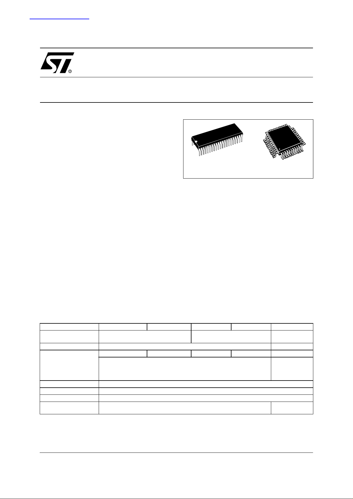
PSDIP42
compare functions
on port B
reset
modes
Windows: Real-Time Emulator, EPROM
Programming Board and Gang Programmer
compiler, source level debugger)
Device Summary
Features ST72(T/E)774 (J/S)9 ST72(T)754(J /S)9 ST72774(J/S)7 ST72754(J/S )7 ST72(T/E)734J6
Program Memory Bytes
RAM (stack) - Bytes 1K (256) 512 (256)
USB No USB USB No USB No USB
Peripherals
Operating Supply 4.0V to 5.5V supply operating range
Oscillator Frequency 12 or 24 MHz
Operating Temperature 0 to +70°C
Package CSDIP42 or PSDIP42 or TQFP44
(1) On some devices only, refer to Device Summ ary; (2) Contact Sales office for availability
(3) 8-bit ±2 LSB A/D converter ; (4) 8-bit ±4 LSB A/D converter.
ADC
3
60K 48K 32K
, 16-bit timer, I2C, DDC, TMU,Sync, PWM, LVD, Watchdog
TQFP44
10 x 10
4
, I2C,LVD,
ADC
DDC,Sync,
16-bit timer,
PWM, Watchdog
PSDIP42
CSDIP42
2
C
October 2003 1/144
1
Page 2

Table of Contents
1 GENERAL DESCRIPTION . . . . . . . . . . . . . . . . . . . . . . . . . . . . . . . . . . . . . . . . . . . . . . . . . . . . . . 6
1.1 INTRODUCTION . . . . . . . . . . . . . . . . . . . . . . . . . . . . . . . . . . . . . . . . . . . . . . . . . . . . . . . . . 6
1.2 PIN DESCRIPTION . . . . . . . . . . . . . . . . . . . . . . . . . . . . . . . . . . . . . . . . . . . . . . . . . . . . . . . 7
1.3 MEMORY MAP . . . . . . . . . . . . . . . . . . . . . . . . . . . . . . . . . . . . . . . . . . . . . . . . . . . . . . . . . 10
1.4 EXTERNAL CONNECTIONS . . . . . . . . . . . . . . . . . . . . . . . . . . . . . . . . . . . . . . . . . . . . . . . 14
2 CENTRAL PROCESSING UNIT . . . . . . . . . . . . . . . . . . . . . . . . . . . . . . . . . . . . . . . . . . . . . . . . . 15
2.1 INTRODUCTION . . . . . . . . . . . . . . . . . . . . . . . . . . . . . . . . . . . . . . . . . . . . . . . . . . . . . . . . 15
2.2 MAIN FEATURES . . . . . . . . . . . . . . . . . . . . . . . . . . . . . . . . . . . . . . . . . . . . . . . . . . . . . . . 15
2.3 CPU REGISTERS . . . . . . . . . . . . . . . . . . . . . . . . . . . . . . . . . . . . . . . . . . . . . . . . . . . . . . . 15
3 CLOCKS, RESET, INTERRUPTS & LOW POWER MODES . . . . . . . . . . . . . . . . . . . . . . . . . . . 18
3.1 CLOCK SYSTEM . . . . . . . . . . . . . . . . . . . . . . . . . . . . . . . . . . . . . . . . . . . . . . . . . . . . . . . . 18
3.1.1 General Description . . . . . . . . . . . . . . . . . . . . . . . . . . . . . . . . . . . . . . . . . . . . . . . . . 18
3.1.2 Crystal Resonator . . . . . . . . . . . . . . . . . . . . . . . . . . . . . . . . . . . . . . . . . . . . . . . . . . 19
3.1.3 External Clock . . . . . . . . . . . . . . . . . . . . . . . . . . . . . . . . . . . . . . . . . . . . . . . . . . . . . 19
3.2 RESET . . . . . . . . . . . . . . . . . . . . . . . . . . . . . . . . . . . . . . . . . . . . . . . . . . . . . . . . . . . . . . . . 20
3.2.1 LVD and Watchdog Reset . . . . . . . . . . . . . . . . . . . . . . . . . . . . . . . . . . . . . . . . . . . . 20
3.2.2 External Reset . . . . . . . . . . . . . . . . . . . . . . . . . . . . . . . . . . . . . . . . . . . . . . . . . . . . . 20
3.2.3 Illegal Address Detection . . . . . . . . . . . . . . . . . . . . . . . . . . . . . . . . . . . . . . . . . . . . . 20
3.2.4 Illegal Opcode Detection . . . . . . . . . . . . . . . . . . . . . . . . . . . . . . . . . . . . . . . . . . . . . 20
3.3 INTERRUPTS . . . . . . . . . . . . . . . . . . . . . . . . . . . . . . . . . . . . . . . . . . . . . . . . . . . . . . . . . . 22
3.4 POWER SAVING MODES . . . . . . . . . . . . . . . . . . . . . . . . . . . . . . . . . . . . . . . . . . . . . . . . . 25
3.4.1 WAIT Mode . . . . . . . . . . . . . . . . . . . . . . . . . . . . . . . . . . . . . . . . . . . . . . . . . . . . . . . 25
3.4.2 HALT Mode . . . . . . . . . . . . . . . . . . . . . . . . . . . . . . . . . . . . . . . . . . . . . . . . . . . . . . . 25
3.5 MISCELLANEOUS REGISTER . . . . . . . . . . . . . . . . . . . . . . . . . . . . . . . . . . . . . . . . . . . . . 26
4 ON-CHIP PERIPHERALS . . . . . . . . . . . . . . . . . . . . . . . . . . . . . . . . . . . . . . . . . . . . . . . . . . . . . . 2 7
4.1 I/O PORTS . . . . . . . . . . . . . . . . . . . . . . . . . . . . . . . . . . . . . . . . . . . . . . . . . . . . . . . . . . . . . 27
4.1.1 Introduction . . . . . . . . . . . . . . . . . . . . . . . . . . . . . . . . . . . . . . . . . . . . . . . . . . . . . . . 27
4.1.2 Common Functional Description . . . . . . . . . . . . . . . . . . . . . . . . . . . . . . . . . . . . . . . 28
4.1.3 Port A . . . . . . . . . . . . . . . . . . . . . . . . . . . . . . . . . . . . . . . . . . . . . . . . . . . . . . . . . . . . 29
4.1.4 Port B . . . . . . . . . . . . . . . . . . . . . . . . . . . . . . . . . . . . . . . . . . . . . . . . . . . . . . . . . . . . 31
4.1.5 Port C . . . . . . . . . . . . . . . . . . . . . . . . . . . . . . . . . . . . . . . . . . . . . . . . . . . . . . . . . . . . 33
4.1.6 Port D . . . . . . . . . . . . . . . . . . . . . . . . . . . . . . . . . . . . . . . . . . . . . . . . . . . . . . . . . . . . 35
4.1.7 Register Description . . . . . . . . . . . . . . . . . . . . . . . . . . . . . . . . . . . . . . . . . . . . . . . . . 38
4.2 WATCHDOG TIMER (WDG) . . . . . . . . . . . . . . . . . . . . . . . . . . . . . . . . . . . . . . . . . . . . . . . 39
4.2.1 Introduction . . . . . . . . . . . . . . . . . . . . . . . . . . . . . . . . . . . . . . . . . . . . . . . . . . . . . . . 39
4.2.2 Main Features . . . . . . . . . . . . . . . . . . . . . . . . . . . . . . . . . . . . . . . . . . . . . . . . . . . . . 39
4.2.3 Functional Description . . . . . . . . . . . . . . . . . . . . . . . . . . . . . . . . . . . . . . . . . . . . . . . 39
4.2.4 Interrupts . . . . . . . . . . . . . . . . . . . . . . . . . . . . . . . . . . . . . . . . . . . . . . . . . . . . . . . . . 40
4.2.5 Register Description . . . . . . . . . . . . . . . . . . . . . . . . . . . . . . . . . . . . . . . . . . . . . . . . . 40
4.3 16-BIT TIMER (TIM) . . . . . . . . . . . . . . . . . . . . . . . . . . . . . . . . . . . . . . . . . . . . . . . . . . . . . . 41
4.3.1 Introduction . . . . . . . . . . . . . . . . . . . . . . . . . . . . . . . . . . . . . . . . . . . . . . . . . . . . . . . 41
4.3.2 Main Features . . . . . . . . . . . . . . . . . . . . . . . . . . . . . . . . . . . . . . . . . . . . . . . . . . . . . 41
4.3.3 Functional Description . . . . . . . . . . . . . . . . . . . . . . . . . . . . . . . . . . . . . . . . . . . . . . . 41
4.3.4 Register Description . . . . . . . . . . . . . . . . . . . . . . . . . . . . . . . . . . . . . . . . . . . . . . . . . 51
4
4.4 SYNC PROCESSOR (SYNC) . . . . . . . . . . . . . . . . . . . . . . . . . . . . . . . . . . . . . . . . . . . . . . 56
2/144
2
Page 3

ST72774/ST727754/ST72734
4.4.1 Introduction . . . . . . . . . . . . . . . . . . . . . . . . . . . . . . . . . . . . . . . . . . . . . . . . . . . . . . . 56
4.4.2 Main Features . . . . . . . . . . . . . . . . . . . . . . . . . . . . . . . . . . . . . . . . . . . . . . . . . . . . . 56
4.4.3 Input Signals . . . . . . . . . . . . . . . . . . . . . . . . . . . . . . . . . . . . . . . . . . . . . . . . . . . . . . 57
4.4.4 Input Signal Waveforms . . . . . . . . . . . . . . . . . . . . . . . . . . . . . . . . . . . . . . . . . . . . . . 57
4.4.5 Output Signals . . . . . . . . . . . . . . . . . . . . . . . . . . . . . . . . . . . . . . . . . . . . . . . . . . . . . 57
4.4.6 Input Processing . . . . . . . . . . . . . . . . . . . . . . . . . . . . . . . . . . . . . . . . . . . . . . . . . . . 61
4.4.7 Output Processing . . . . . . . . . . . . . . . . . . . . . . . . . . . . . . . . . . . . . . . . . . . . . . . . . . 64
4.4.8 Analyzer Mode . . . . . . . . . . . . . . . . . . . . . . . . . . . . . . . . . . . . . . . . . . . . . . . . . . . . . 65
4.4.9 Corrector Mode . . . . . . . . . . . . . . . . . . . . . . . . . . . . . . . . . . . . . . . . . . . . . . . . . . . . 67
4.4.10Register Description . . . . . . . . . . . . . . . . . . . . . . . . . . . . . . . . . . . . . . . . . . . . . . . . . 68
4.5 TIMING MEASUREMENT UNIT (TMU) . . . . . . . . . . . . . . . . . . . . . . . . . . . . . . . . . . . . . . . 75
4.5.1 Introduction . . . . . . . . . . . . . . . . . . . . . . . . . . . . . . . . . . . . . . . . . . . . . . . . . . . . . . . 75
4.5.2 Main Features . . . . . . . . . . . . . . . . . . . . . . . . . . . . . . . . . . . . . . . . . . . . . . . . . . . . . 75
4.5.3 Functional Description . . . . . . . . . . . . . . . . . . . . . . . . . . . . . . . . . . . . . . . . . . . . . . . 75
4.5.4 Register Description . . . . . . . . . . . . . . . . . . . . . . . . . . . . . . . . . . . . . . . . . . . . . . . . . 77
4.6 USB INTERFACE (USB) . . . . . . . . . . . . . . . . . . . . . . . . . . . . . . . . . . . . . . . . . . . . . . . . . . 79
4.6.1 Introduction . . . . . . . . . . . . . . . . . . . . . . . . . . . . . . . . . . . . . . . . . . . . . . . . . . . . . . . 79
4.6.2 Main Features . . . . . . . . . . . . . . . . . . . . . . . . . . . . . . . . . . . . . . . . . . . . . . . . . . . . . 79
4.6.3 Functional Description . . . . . . . . . . . . . . . . . . . . . . . . . . . . . . . . . . . . . . . . . . . . . . . 79
4.6.4 Register Description . . . . . . . . . . . . . . . . . . . . . . . . . . . . . . . . . . . . . . . . . . . . . . . . . 80
4.6.5 Programming Considerations . . . . . . . . . . . . . . . . . . . . . . . . . . . . . . . . . . . . . . . . . 85
4.7 I²C SINGLE MASTER BUS INTERFACE (I2C) . . . . . . . . . . . . . . . . . . . . . . . . . . . . . . . . . 87
4.7.1 Introduction . . . . . . . . . . . . . . . . . . . . . . . . . . . . . . . . . . . . . . . . . . . . . . . . . . . . . . . 87
4.7.2 Main Features . . . . . . . . . . . . . . . . . . . . . . . . . . . . . . . . . . . . . . . . . . . . . . . . . . . . . 87
4.7.3 General Description . . . . . . . . . . . . . . . . . . . . . . . . . . . . . . . . . . . . . . . . . . . . . . . . . 87
4.7.4 Functional Description (Master Mode) . . . . . . . . . . . . . . . . . . . . . . . . . . . . . . . . . . . 89
4.7.5 Register Description . . . . . . . . . . . . . . . . . . . . . . . . . . . . . . . . . . . . . . . . . . . . . . . . . 91
4.8 DDC INTERFACE (DDC) . . . . . . . . . . . . . . . . . . . . . . . . . . . . . . . . . . . . . . . . . . . . . . . . . . 95
4.8.1 Introduction . . . . . . . . . . . . . . . . . . . . . . . . . . . . . . . . . . . . . . . . . . . . . . . . . . . . . . . 95
4.8.2 DDC Interface Features . . . . . . . . . . . . . . . . . . . . . . . . . . . . . . . . . . . . . . . . . . . . . . 95
4.8.3 Sig nal Description . . . . . . . . . . . . . . . . . . . . . . . . . . . . . . . . . . . . . . . . . . . . . . . . . . 97
4.8.4 I2C BUS Protocol . . . . . . . . . . . . . . . . . . . . . . . . . . . . . . . . . . . . . . . . . . . . . . . . . . . 98
4.8.5 DDC Standard . . . . . . . . . . . . . . . . . . . . . . . . . . . . . . . . . . . . . . . . . . . . . . . . . . . . . 99
4.8.6 Register Description . . . . . . . . . . . . . . . . . . . . . . . . . . . . . . . . . . . . . . . . . . . . . . . . 110
4.9 PWM/BRM GENERATOR (DAC) . . . . . . . . . . . . . . . . . . . . . . . . . . . . . . . . . . . . . . . . . . . 116
4.9.1 Introduction . . . . . . . . . . . . . . . . . . . . . . . . . . . . . . . . . . . . . . . . . . . . . . . . . . . . . . 116
4.9.2 Main Features . . . . . . . . . . . . . . . . . . . . . . . . . . . . . . . . . . . . . . . . . . . . . . . . . . . . 116
4.9.3 Functional Description . . . . . . . . . . . . . . . . . . . . . . . . . . . . . . . . . . . . . . . . . . . . . . 116
4.9.4 Register Description . . . . . . . . . . . . . . . . . . . . . . . . . . . . . . . . . . . . . . . . . . . . . . . . 121
4.108-BIT A/D CONVERTER (ADC) . . . . . . . . . . . . . . . . . . . . . . . . . . . . . . . . . . . . . . . . . . . . 123
4.10.1 Int roducti on . . . . . . . . . . . . . . . . . . . . . . . . . . . . . . . . . . . . . . . . . . . . . . . . . . . . . . 123
4.10.2Main Features . . . . . . . . . . . . . . . . . . . . . . . . . . . . . . . . . . . . . . . . . . . . . . . . . . . . 123
4.10.3 F unct ional Description . . . . . . . . . . . . . . . . . . . . . . . . . . . . . . . . . . . . . . . . . . . . . . 123
4.10.4Low Power Mode . . . . . . . . . . . . . . . . . . . . . . . . . . . . . . . . . . . . . . . . . . . . . . . . . 124
4.10.5Interrupts . . . . . . . . . . . . . . . . . . . . . . . . . . . . . . . . . . . . . . . . . . . . . . . . . . . . . . . . 124
4.10.6Register Description . . . . . . . . . . . . . . . . . . . . . . . . . . . . . . . . . . . . . . . . . . . . . . . . 125
5 INSTRUCTION SET . . . . . . . . . . . . . . . . . . . . . . . . . . . . . . . . . . . . . . . . . . . . . . . . . . . . . . . . . 126
5.1 ST7 ADDRESSING MODES . . . . . . . . . . . . . . . . . . . . . . . . . . . . . . . . . . . . . . . . . . . . . . 126
3/144
Page 4

ST72774/ST727754/ST72734
5.1.1 Inherent . . . . . . . . . . . . . . . . . . . . . . . . . . . . . . . . . . . . . . . . . . . . . . . . . . . . . . . . . 127
5.1.2 Imme diate . . . . . . . . . . . . . . . . . . . . . . . . . . . . . . . . . . . . . . . . . . . . . . . . . . . . . . . 127
5.1.3 Direct . . . . . . . . . . . . . . . . . . . . . . . . . . . . . . . . . . . . . . . . . . . . . . . . . . . . . . . . . . . 127
5.1.4 Indexed (No Offset, Short, Long) . . . . . . . . . . . . . . . . . . . . . . . . . . . . . . . . . . . . . . 127
5.1.5 Indirect (Short, Long) . . . . . . . . . . . . . . . . . . . . . . . . . . . . . . . . . . . . . . . . . . . . . . . 127
5.1.6 Indirect Indexed (Short, Long) . . . . . . . . . . . . . . . . . . . . . . . . . . . . . . . . . . . . . . . . 128
5.1.7 Relative mode (Direct, Indirect) . . . . . . . . . . . . . . . . . . . . . . . . . . . . . . . . . . . . . . . 128
5.2 INSTRUCTION GROUPS . . . . . . . . . . . . . . . . . . . . . . . . . . . . . . . . . . . . . . . . . . . . . . . . 129
6 ELECTRICAL CHARACTERISTICS . . . . . . . . . . . . . . . . . . . . . . . . . . . . . . . . . . . . . . . . . . . . . 132
6.1 POWER CONSIDERATIONS . . . . . . . . . . . . . . . . . . . . . . . . . . . . . . . . . . . . . . . . . . . . . 133
6.2 AC/DC ELECTRICAL CHARACTERISTICS . . . . . . . . . . . . . . . . . . . . . . . . . . . . . . . . . . 134
7 GENERAL INFORMATION . . . . . . . . . . . . . . . . . . . . . . . . . . . . . . . . . . . . . . . . . . . . . . . . . . . . 139
7.1 PACKAGE MECHANICAL DATA . . . . . . . . . . . . . . . . . . . . . . . . . . . . . . . . . . . . . . . . . . . 139
8 ORDERING INFORMATION . . . . . . . . . . . . . . . . . . . . . . . . . . . . . . . . . . . . . . . . . . . . . . . . . . . 141
8.1 TRANSFER OF CUSTOMER CODE . . . . . . . . . . . . . . . . . . . . . . . . . . . . . . . . . . . . . . . . 141
4/144
Page 5

Revision follow-up
Changes applied since version 4.0
Version 4.0 March 2001
Page 1:Addition of 72T774 (32KOTP).
Addition of 60K/48K ROM for ST72754
Deletion of table “ device summary”, replaced with cross reference to table 36 on page 147.
page 13 - addition of section 1.4. external connections
Version 4.1 July 2001
Initial format reapplied, text and related figures in the same page.
Table “Device summary” reinserted in cover page and updated.
Update of table 36: ordering information (p143)
Version 4.2 July 2001
Cover - addition of feature about system protection added,
table for device summary: addition of stack values
page 9 - figure 3: replaced 1KByte with 512 Bytes + notes about opcode fetch and HALT
mode
page 10 - table: CR replaced by WDGCR
TIM replaced with Timer and WDG replaced with Watchdog
page 115 - EDF register: addition of “read from RAM”, EDE: few changes
page 135 - Note 1 replaced, note 2 added SUSpend mode limitation..
Whole document: all mentions of HALT mode either deleted or rewritten.
Version 4.3 October 2001
p140, chapter 8, section 8.1code for unused bytes ( FFh) replaced with
page 141- update of table 36 “Ordering information”
page 142 - list of available devices updated
page 114 - DDC DCR register: bit 5 = 1, text “or read from RAM” deleted
Version 4.3 November 2001
page 10, one adddress corrected in the figure 3 “memory map”: 0400h
page 14: addition of mandatory 1K resistor (text and figure)
ST72774/ST727754/ST72734
9Dh (opcode for NOP)
5/144
3
Page 6
ST72774/ST727754/ST72734
1 GENERAL DESCRIPTION
1.1 INTRODUCTION
The ST72774, ST72754 and ST72734 are
HCMOS microcontroller units (MCU) from the
ST727x4 family with dedicated peripherals for
Monitor applications.
They are based around an industry standard 8-bit
core and offer an enhanced instruction set. The
processor runs with an external clock at 12 or 24
MHz with a 5V supply. Due to the fully static design
of this device, operation do wn to DC is possible.
Under software control the ST727x4 can be placed
in WAIT mode thus reducing p ower consumpt ion.
The HALT mode is no longer available.
The enhanced instruction set and addressing
modes afford real programming potential. Illegal
opcodes are patched and lead to a reset.
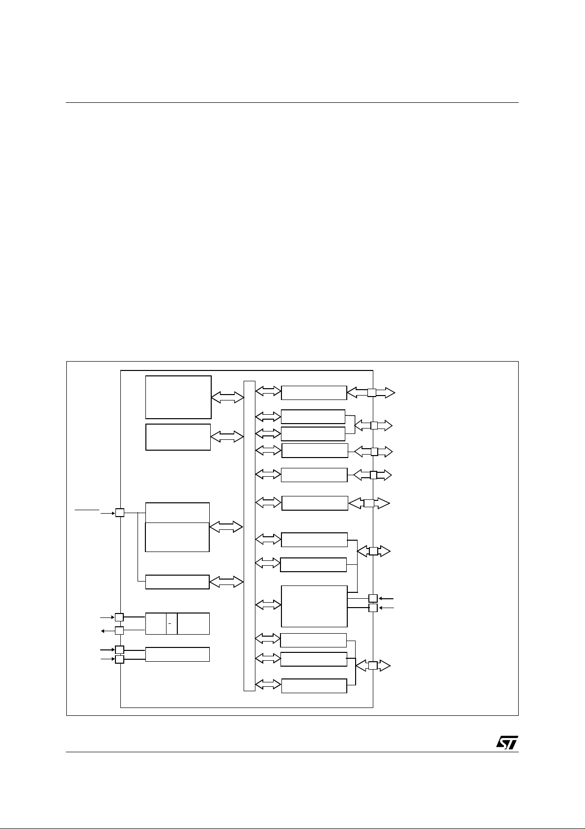
Figure 1. ST727x4 Block Diagram
Up to 60K Bytes
ROM/OTP/EPROM
Up to 1K Bytes
RAM
In addition to standard 8-bit data management the
ST7 features true bit manipulation, 8x8 unsigned
multiplication and indirect addressing modes.
The device includes an on-chip oscillator, CPU,
System protection aga inst illeg al add re ss j umps,
Sync Processor for video timing & Vfback analysis,
up to 60K Program Mem ory, up to 1K RAM, US B/
DMA, a Timing Measurement Unit, I/O, a timer with
2 input captures and 2 output compares, a 4channel Analog to Digital Converter, DDC, I
Single Master, W atchdog Reset, and ei ght 10-bit
PWM/BRM outputs for analog DC control of
external functions.
PA0/OCMP1
PA1
PORT A
PORT B
ADC
I2C
PA2/VSYNCI2
PA3-PA6
PA7/BLANKOUT
PB6-PB7/AIN2-AIN 3/ PWM1- PWM2
PB4-PB5/AIN0-AIN1
PB3/SDAI
PB2/SCLI
2
C
RESET
OSCIN
OSCOUT
V
V
6/144
DD
SS
CONTROL
8-BIT CO RE
ALU
WATCHDOG
Mode
3
:
OSC
Selection
POWER SUPPLY
DDC
ADDRESS AND DATA BUS
USB
PORT D
TIMER
SYNC
PROCESSOR
TMU
PORT C
DAC (PWM)
PB1/SDAD
PB0/SCLD
USBVCC
USBDP
USBDM
PD0/VSYNCO
PD1/HSYNCO
PD2/CSYNCI
PD3/ITA/VFBACK
PD4/ITB
PD5/HFBACK
PD6/CLAMPOUT
VSYNCI
HSYNCI
PC0/HSYNCDIV
PC1/AV
PC2-PC7/PWM3-PWM8
3
Page 7
1.2 PIN DESCRI PTION
Figure 2. 44-pin TQFP and 42-Pin SDIP Package Pinouts
PC1 / AV
PC0 / HSYNCDIV
PA0 / O C MP1
PWM7 / PC6
PWM8 / PC7
PWM2 / AIN3 / PB7
PWM1 / AIN2 / PB6
AIN1 / PB5
AIN0 / PB4
NC
V
DD
USBVCC
USBDM
USBDP
PC5 / PWM6
PC4 / PWM5
PC3 / PWM4
PC2 / PWM3
44 43 42 41 40 39 38 37 36 35 34
1
2
3
4
5
6
7
8
9
10
11
12 13 14 15 16 17 18 19 20 21 22
ss
V
TEST / VPPRESET
PA1
ST72774/ST727754/ST72734
PA2/VSYNCI2
PA3
33
PA4
32
PA5
31
PA6
30
OSCIN
29
OSCOUT
28
PA7 / BLANKO UT
27
PB3 / SDAI
26
PB2 / SCLI
25
PB1 / SDAD
24
NC
23
HSYNCDIV / PC0
AV / PC1
PWM3 / PC2
PWM4 / PC3
PWM5 / PC4
PWM6 / PC5
PWM7 / PC6
PWM8 / PC7
PWM2 / AIN3 / PB7
PWM1 / AIN2 / PB6
AIN1 / PB5
AIN0 / PB4
V
DD
USBVCC
USBDM
USBDP
V
SS
HSYNCI
VSYNCI
VSYNCO / PD0
HSYNCO / PD1
VSYNCI
HSYNCI
VSYNCO / PD0
HSYNCO / PD1
1
2
3
4
5
6
7
8
9
10
11
12
13
14
15
16
17
18
19
20
21
ITB / PD4
CSYNCI / PD2
VFBACK / IT A /PD3
42
41
40
39
38
37
36
35
34
33
32
31
30
29
28
27
26
25
24
23
22
SCLD / PB0
HFBACK / PD5
CLAMPOUT / PD6
PA0 / OCMP1
TEST / V
RESET
PA1
PA2/VSYNCI2
PA3
PA4
PA5
PA6
OSCIN
OSCOUT
PA7 / BLANKOUT
PB3 / SDAI
PB2 / SCLI
PB1 / SDAD
PB0 / SCLD
PD6 / CLAMPOUT
PD5 / HFBACK
PD4 / ITB
PD3 / ITA / VFBACK
PD2 / CSYNCI
PP
NC = Not connected
7/144
3
Page 8
ST72774/ST727754/ST72734
PIN DESCRIPTION (Cont’d)
RESET:
Bidirectional. This active low signal forces
the initialization of the MCU. This event is the top
priority non maskable interrupt. This pin is
switched low when the Watchdog has triggered or
V
is low. It can be used to reset external
DD
peripherals.
OSCIN/OSCOUT: Input/Output Oscillator pin.
These pins connect a pa rallel-resonant crystal, or
an external sou rc e to the on -c h ip o s cilla t o r.
TEST/V
: Input. EPROM programming voltage.
PP
This pin must be held low during normal operating
modes.
V
: Power supply voltage (4.0V-5.5V)
DD
V
: Digital Ground.
SS
Alter nate Funct ions: several pins of the I/O ports
assume software programmable alternate
functions as shown in the pin description
Table 1. ST727x4 Pin Description
Pin No.
Pin Name
SDIP42
TQFP44
39 1 PC0/HSYNCDIV I/O Port C0 or HSYNCDIV output (HSYNCO divided by 2)
40 2 PC1/AV I/O Port C1 or “Active Video” input
41 3 PC2/PWM3 I/O Port C2 or 10-bit PWM/BRM output 3
42 4 PC3/PWM4 I/O Port C3 or 10-bit PWM/BRM output 4
43 5 PC4/PWM5 I/O Port C4 or 10-bit PWM/BRM output5
44 6 PC5/PWM6 I/O Port C5 or 10-bit PWM/BRM output 6
1 7 PC6/PWM7 I/O Port C6 or 10-bit PWM/BRM output 7
2 8 PC7/PWM8 I/O Port C7 or 10-bit PWM/BRM output 8
3 9 PB7/AIN3/PWM2 I/O
4 10 PB6/AIN2/PWM1 I/O
5 11 PB5/AIN1 I/O Port B5 or ADC analog input 1
6 12 PB4/AIN0 I/O Port B4 or ADC analog input 0
813V
9 14 USBVCC S USB power supply (output 3.3V +/- 10%)
10 15 USBDM I/O USB bidirectional data Must be tied to ground
11 16 USBDP I/O USB bidirectional data
12 17 V
13 18 HSYNCI I SYNC horizontal synchronisation input
14 19 VSYNCI I SYN C vertical synch ronis ation input
15 20 PD0/VSYNCO I/O Port D0 or SYNC vertical synchronisation output
16 21 PD1/HSYNCO I/O Port D1 or SYNC horizontal synchronisation output
17 22 PD2/CSYNCI I/O Port D2 or SYNC composite synchronisation input
DD
SS
Type
Port B7 or ADC analog input 3 or 10-bit PWM/BRM
output 2
Port B6 or ADC analog input 2 or 10-bit PWM/BRM
output 1
S Supply (4.0V - 5.5V)
S Ground 0V
Description Remarks
For analog controls,
after external filtering
for devices without
USB peripheral
TTL levels
Refer to Figure 16
TTL levels with pull-up
(SYNC input)
8/144
3
Page 9

Pin No.
ST72774/ST727754/ST72734
Pin Name
SDIP42
TQFP44
18 23 PD3/VFBACK/ITA I/O
19 24 PD4/ITB I/O Port D4 or Interrupt falling edge detector input B
20 25 PD5/HFBACK I/O Port D5 or SYNC horizontal flyback input
21 26 PD6/CLAMPOUT I/O Port D6 or SYNC clamping/ MOIRE output
22 27 PB0/SCLD I/O Port B0 or DDC serial clock
24 28 PB1/SDAD I/O Port B1 or DDC serial data
25 29 PB2/SCLI I/O Port B2 or I2C serial clock
26 30 PB3/SDAI I/O Port B3 or I2C serial data
27 31 PA7/BLANKOUT I/O Port A7 or SYNC blanking output
28 32 OSCOUT O Oscillator output
29 33 OSCIN I Oscillator input
30 34 PA6 I/O Port A6
31 35 PA5 I/O Port A5
32 36 PA4 I/O Port A4
33 37 PA3 I/O Port A3
34 38 PA2/VSYNCI2 I/O Port A2 or SYNC vertical synchronisation input 2 DDC1 only
35 39 PA1 I/O Port A1
36 40 RESET
37 41 TEST/V
38 42 PA0/OCMP1 I/O Port A0 or TIMER output compare 1
PP
Type
Port D3 or SYNC Vertical flyback input or interrupt falling edge detector input A
I/O Reset pin Active low
Test mode pin or EPROM programming voltage. This
S
pin should be tied low in user mode.
Description Remarks
Refer to Figure 16 and
Table 11 Port D Description
Refer to Table 11 Port
D Description
TTL levels with pull-up
(SYNC input)
9/144
Page 10
ST72774/ST727754/ST72734
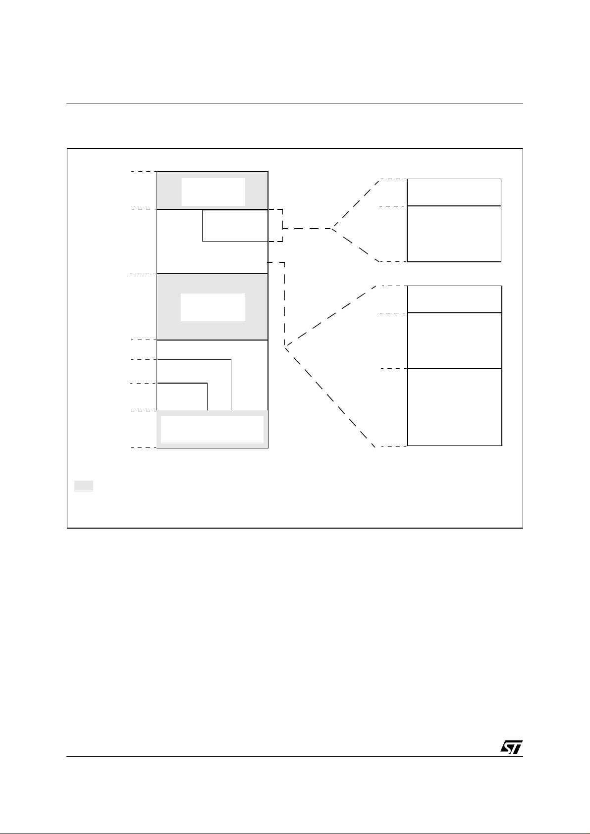
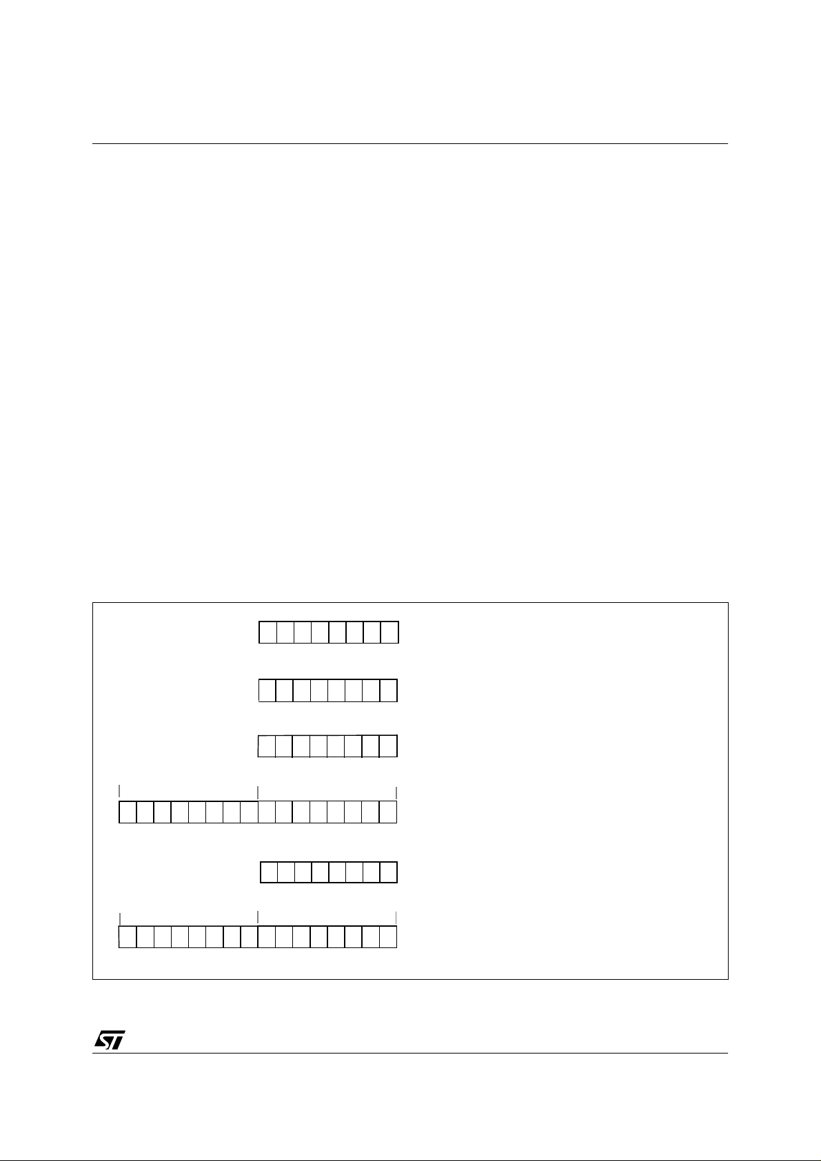
1.3 MEMORY MA P
Figure 3. Me m ory Map
0000h
005Fh
0060h
03FFh
0400h
0FFFh
1000h
4000h
8000h
FFDFh
FFE0h
FFFFh
HW Registers
(see Table 2)
512 Bytes RAM
1 Kbyte RAM
Reserved
60 Kbytes
ROM/EPROM
48 Kbytes
32 Kbytes
Interrupt & Reset Vectors *
(see Table 3)
0060h
0100h
01FFh
0060h
0100h
01FFh
0200h
03FFh
Short Addressing
RAM (zero page)
256 Bytes Stack/
16-bit Addressing RAM
Short Addressing
RAM (zero page)
256 Bytes Stack/
16-bit Addressing RAM
16-bit Addressing
RAM
512 Bytes
any opcode fetch in those areas is considered as illegal and generates a reset
(*) this block only contains addresses of interrupts and reset routines, no opcode is run from this block
10/144
Page 11
MEMORY MAP (Cont’d)
Table 2. Hardware Register Mem ory Map
ST72774/ST727754/ST72734
Address Block Register Label Register Name
0000h
0001h
0002h
0003h
0004h
0005h
0006h
0007h
0008h Watchdog WDGCR Watchdog Control Register 7Fh R/W
0009h MISCR Miscellaneous Register 10h R/W
000Ah
000Bh
000Ch
000Dh
000Eh
000Fh
00010h
0011h
0012h
0013h
0014h
0015h
0016h
0017h
0018h
0019h
001Ah
001Bh
001Ch
001Dh
001Eh
001Fh
0020h
to
0024h
ADC
DDC1/2B
TMU
Timer
PADR
PADDR
PBDR
PBDDR
PCDR
PCDDR
PDDR
PDDDR
ADCDR
ADCCSR
DDCDCR
DDCAHR
TMUCSR
TMUT1CR
TMUT2CR
TIMCR2
TIMCR1
TIMSR
TIMIC1HR
TIMIC1LR
TIMOC1HR
TIMOC1LR
TIMCHR
TIMCLR
TIMACHR
TIMACLR
TIMIC2HR
TIMIC2LR
TIMOC2HR
TIMOC2LR
Port A Data Register
Port A Data Direction Register
Port B Data Register
Port B Data Direction Register
Port C Data Register
Port C Data Direction Register
Port D Data Register
Port D Data Direction Register
ADC Data Register
ADC Control Status register
DDC1/2B Control Register
DDC1/2B Address Pointer High Register
TMU control status register
TMU T1 counter register
TMU T2 counter register
Timer Control Register 2
Timer Control Register 1
Timer Status Register
Timer Input Capture 1 High Register
Timer Input Capture 1 Low Register
Timer Output Compare 1 High Register
Timer Output Compare 1 Low Register
Timer Counter High Register
Timer Counter Low Register
Timer Alternate Counter High Register
Timer Alternate Counter Low Register
Timer Input Capture 2 High Register
Timer Input Capture 2 Low Register
Timer Output Compare 2 High Register
Timer Output Compare 2 Low Register
Reserved Area (5 bytes)
Status
00h
00h
00h
00h
00h
00h
00h
00h
00h
00h
00h
xxh
FCh
FFh
FFh
00h
00h
00h
xxh
xxh
80h
00h
FFh
FCh
FFh
FCh
xxh
xxh
80h
00h
Reset
R/W
R/W
R/W
R/W
R/W
R/W
R/W
R/W
Read only
R/W
R/W
R/W
R/W
Read only
Read only
R/W
R/W
Read only
Read only
Read only
R/W
R/W
Read only
R/W
Read only
R/W
Read only
Read only
R/W
R/W
Remarks
11/144
Page 12

ST72774/ST727754/ST72734
Address Block Register Label Register Name
0025h
0026h
0027h
0028h
0029h
002Ah
002Bh
002Ch
002Dh
002Eh
002Fh
0030h
0031h
0032h
0033h
0034h
0035h
0036h
0037h
0038h
0039h
003Ah
003Bh
003Ch
003Dh
003Eh
003Fh Reserved Area (1 byte)
0040h
0041h
0042h
0043h
0044h
0045h
0046h
0047h
0048h
to
004Fh
USB
PWM
SYNC
USBPIDR
USBDMAR
USBIDR
USBISTR
USBIMR
USBCTLR
USBDADDR
USBEP0RA
USBEP0RB
USBEP1RA
USBEP1RB
USBEP2RA
USBEP2RB
PWM1
BRM21
PWM2
PWM3
BRM43
PWM4
PWM5
BRM65
PWM6
PWM7
BRM87
PWM8
PWMCR
SYNCCFGR
SYNCMCR
SYNCCCR
SYNCPOLR
SYNCLATR
SYNCHGENR
SYNCVGENR
SYNCENR
USB PID Register
USB DMA address Register
USB Interrupt/DMA Register
USB Interrupt Status Register
USB Interrupt Mask Register
USB Control Register
USB Device Address Register
USB Endpoint 0 Register A
USB Endpoint 0 Register B
USB Endpoint 1 Register A
USB Endpoint 1 Register B
USB Endpoint 2 Register A
USB Endpoint2 Register B
10 BIT PWM / BRM
PWM output enable register
SYNC Configuration Register
SYNC Multiplexer Register
SYNC Counter Register
SYNC Polarity Register
SYNC Latch Register
SYNC H Sync Generator Register
SYNC V Sync Generator Register
SYNC Processor Enable Register
Reserved Area (8 bytes)
Reset
Status
XXh
XXh
XXh
00h
00h
xxxx 0110
00h
0000 xxxx
80h
0000 xxxx
0000
xxxx0000
0000
xxxx0000
80h
00h
80h
80h
00h
80h
80h
00h
80h
80h
00h
80h
00h
00h
20h
00h
08h
00h
00h
00h
C3h
Remarks
Read only
R/W
R/W
R/W
R/W
R/W
R/W
R/W
R/W
R/W
R/W
R/W
R/W
R/W
R/W
R/W
R/W
R/W
R/W
R/W
R/W
R/W
R/W
R/W
R/W
R/W
R/W
R/W
R/W
R/W
R/W
R/W
R/W
R/W
12/144
Page 13
ST72774/ST727754/ST72734
Address Block Register Label Register Name
0050h
0051h
0052h
0053h
0054h
0055h
0056h
0057h
0058h
0059h
005Ah
005Bh
005Ch
005Dh
005Eh
005Fh
DDC/CI
I2C
DDCCR
DDCSR1
DDCSR2
DDCOAR
DDCDR
I2CDR
I2CCCR
I2CSR2
I2CSR1
I2CCR
DDC/CI Control Register
DDC/CI Status Register 1
DDC/CI Status Register 2
Reserved
DDC/CI (7 Bits) Slave address Register
Reserved
DDC/CI Data Register
Reserved Area (2 bytes)
I2C Data Register
Reserved
Reserved
2
C Clock Control Register
I
2
C Status Register 2
I
2
C Status Register 1
I
2
C Control Register
I
Reset
Status
00h
00h
00h
00h
00h
00h
00h
00h
00h
00h
Table 3. Interrupt Vector Map
Vector Address Description Remarks
FFE0-FFE1h
FFE2-FFE3h
FFE4-FFE5h
FFE6-FFE7h
FFE8-FFE9h
FFEA-FFEBh
FFEC-FFEDh
FFEE-FFEFh
FFF0-FFF1h
FFF2-FFF3h
FFF4-FFF5h
FFF6-FFF7h
FFF8-FFF9h
FFFA-FFFBh
FFFC-FFFDh
FFFE-FFFFh
Timer Overflow interrupt vector
Timer Output Compare interrupt vector
Timer Input Capture interrupt vector
ITA falling edge interrupt vector
ITB falling edge interrupt vector
DDC1/2B interrupt vector
USB End Suspend interrupt vector
TRAP (software) interrupt vector
Not used
Not used
Not used
USB interrupt vector
Not used
I2C interrupt vector
DDC/CI interrupt vector
RESET vector
Internal Interrupts
External Interrupts
Internal Interrupt
CPU Interrupt
Remarks
R/W
Read only
Read only
R/W
R/W
R/W
R/W
Read only
Read only
R/W
13/144
Page 14
ST72774/ST727754/ST72734
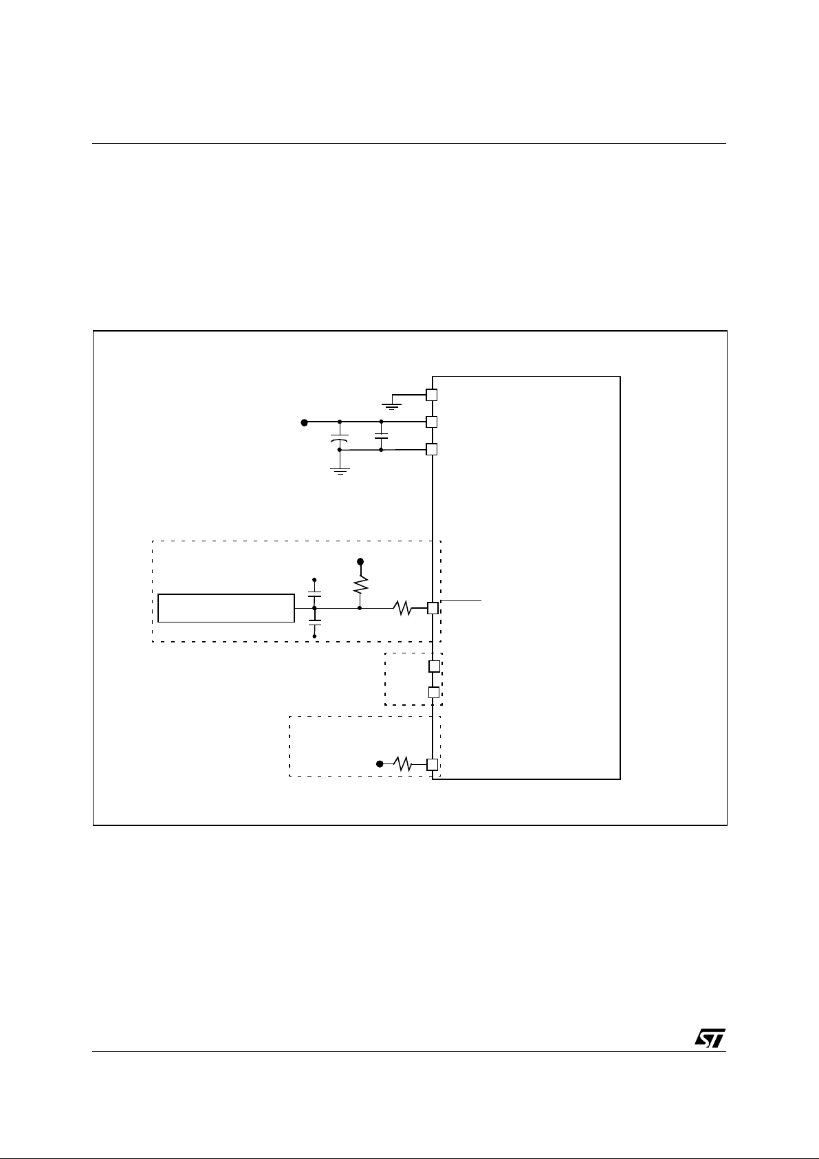
1.4 External connections
The following figure shows the recom mended external connections for the device.
The V
pin is only used for programming OTP
PP
and EPROM devices and must be tied to ground in
user mode.
The 10 nF and 0. 1 µF decoupling capacitors on
the power supply lines are a suggested EMC performance/cost tradeoff.
Figure 4. Recommended Extern al Connec tions
V
DD
EXTERNAL RESET CIRCUIT
10nF
V
DD
0.1µF
0.1µF
+
4.7K
The external reset network (including the mandatory 1K serial resistor) is inten ded to protect the
device against parasitic resets, espec ially in noisy
environments.
Unused I/Os shoul d be t ied hi gh to av oid any unnecessary power consumption on floating lines.
An alternative solution is to program the unused
ports as inputs with pull-up.
V
PP
V
0.1µF
1K
DD
V
SS
RESET
14/144
See
Clocks
Section
Or configure unused I/O ports
by software as input with pull-up
V
10K
DD
OSCIN
OSCOUT
Unused I/O
Page 15
2 CENTRAL PRO CESSING UNIT
ST72774/ST727754/ST72734
2.1 INTRODUCTION
This CPU has a full 8-bit architecture and contains
six internal registers allowing efficient 8-bit data
manipulation.
2.2 MAIN FEATURES
■ 63 basic instructions
■ Fast 8-bit by 8-bit multiply
■ 17 main addressing modes
■ Two 8-bit index registers
■ 16-bit stack pointer
■ Low power modes
■ Maskable hardware interrupts
■ Non-maskable software interrupt
2.3 CPU REGISTERS
The 6 CPU registers shown in Figure 5 are not
present in the memory mapping and are accessed
by specific instructions.
Accumulator (A)
Figure 5. CPU Registers
70
RESET VALUE = XXh
70
RESET VALUE = XXh
70
RESET VALUE = XXh
The Accumulator is an 8-bit general purpose
register used to hold operands and the results of
the arithmetic and logic calculations and to
manipulate data.
Index Registers (X and Y)
In indexed addressing modes, these 8-bit registers
are used to create either effective addresses or
temporary storage areas for data manipulation.
(The Cross-Assembler generates a precede
instruction (PRE) to indicate that the following
instruction refers to the Y register.)
The Y register is not affected by the interrupt
automatic procedures (not pushed to and pop ped
from the stack).
Program Cou nt er (P C )
The program counter is a 16-bit register containing
the address of the next instruction to be executed
by the CPU. It is made of two 8-bit registers PCL
(Program Counter Low which is the LSB) and PCH
(Program Counter High which is the MSB).
ACCUMULATOR
X INDEX REGISTER
Y INDEX REGISTER
15 8
RESET VALUE = RESET VECTOR @ FFFEh-FFFFh
15
RESET VALUE = STACK HIGHER ADDRESS
PCH
RESET VALUE =
7
70
1C11HI NZ
1X11X1XX
70
8
PCL
0
PROGRAM COUNTER
CONDITION CODE REGISTER
STACK POINTER
X = Undefined Value
15/144
Page 16

ST72774/ST727754/ST72734
CPU REGISTERS (Cont’d)
CONDITION CODE REGISTER (CC)
Read/Write
Reset Value: 111x1xxx
70
enter it and reset by the IRET instruction at the end
of the interrupt routine. If the I bit is cleared by
software in the interrupt routine, pending interrupts
are serviced regardless of the pri ority level of the
current interrupt routine.
111HINZC
The 8-bit Condition Code register contains the
interrupt mask and four flags representative of the
result of the instruction just executed. This register
can also be handled by the PUSH and POP
instructions.
These bits can be individually tested and/or
controlled by specific instructions.
Bit 4 = H
Half carry
.
This bit is set by hardware when a carry occurs
between bits 3 and 4 of the ALU during an ADD or
ADC instruction. It is reset by hardware during the
same instructions.
0: No half carry has occurred.
1: A half carry has occurred.
This bit is tested using the JRH or JRNH
instruction. The H bit is useful in B CD arithmetic
subroutines.
Bit 2 = N
Negative
.
This bit is set and cleared by hardware. It is
representative of the result sign of the last
arithmetic, logical or data manipulation. It is a copy
of the 7
th
bit of the result.
0: The result of the last operation is positive or null.
1: The result of the last operation is negative
(i.e. the most significant bit is a logic 1).
This bit is accessed by the JRMI and JRPL
instructions.
Bit 1 = Z
Zero
.
This bit is set and cleared by hardware. This bit
indicates that the result of the last arithmetic,
logical or data manipulation is zero.
0: The result of the last operation is different from
zero.
1: The result of the last operation is zero.
This bit is accessed by the JREQ and JRNE test
instructions.
Bit 3 = I
Interrupt mask
.
This bit is set by hardware when entering in
interrupt or by software to disable all interrupts
except the TRAP software interrupt. This bit is
cleared by software.
0: Interrupts are enabled.
1: Interrupts are disabled.
This bit is controlled by the RIM, SIM and IRET
instructions and is tested by the JRM and JRNM
instructions.
Note: Interrupts requested while I is set are
latched and can be processed whe n I is cleared.
By default an interrupt routine is not in terruptable
because the I bit is set by hardware when you
16/144
Bit 0 = C
Carry/borrow.
This bit is set and cleared by hardware and
software. It indicates an overflow or an underflow
has occurred during the last arithmetic operation.
0: No overflow or underflow has occurred.
1: An overflow or underflow has occurred.
This bit is driven by th e SCF and RCF instructions
and tested by the JRC and JRNC instructions. It is
also affected by the “bit test and branch”, shift and
rotate instructions.
Page 17
ST72774/ST727754/ST72734
CPU REGISTERS (Cont’d)
Stack Pointer (SP)
Read/Write
Reset Value: 01 FFh
15 8
00000001
70
The least significant byte of the Stack Pointer
(called S) can be directly accessed by a LD
instruction.
Note: When the lower limit is exceeded, the Stack
Pointer wraps around to the stack upper limit,
without indicating the stack overflow. The
previously stored information is then overwritten
and therefore lost. The stack also wraps in case of
an underflow.
SP7 SP6 SP5 SP4 SP3 SP2 SP1 SP0
The Stack Pointer is a 16-bit register which is
always pointing to the next free location in the
stack. It is then decremented after data has been
pushed onto the stack and incremented before
data is popped from the stack (see Figure 6).
Since the stack is 256 bytes deep, the most
significant byte is forced by ha rd ware. Fol lowing
an MCU Reset, or after a Reset Stack Pointer
instruction (RSP), the Stack Pointer contains its
reset value (the SP7 to SP0 bits are set) which is
the stack higher address.
Figure 6. Stack Manipulation Example
@ 0100h
SP
@ 01FFh
CALL
Subroutine
PCH
PCL
Interrupt
event
SP
SP
CC
A
X
PCH
PCL
PCH
PCL
PUSH Y POP Y IRET
Y
CC
A
X
PCH
PCL
PCH
PCL
The stack is used to save the return address
during a subroutine call and the CPU context
during an interrupt. The user may also directly
manipulate the stack b y means of the PU SH and
POP instructions. In the case of an in terrupt, the
PCL is stored at the first location pointed to by the
SP. Then the other registers are stored in the next
locations as shown in Figure 6.
– When an interrupt is received, the SP is decre-
mented and the context is pushed on the stack.
– On return from interrupt, the SP is incremented
and the context is popped from the stack.
A subroutine call occupies two locations and an
interrupt five locations in the stack area.
RET
or RSP
SP
CC
A
X
PCH
PCL
PCH
PCL
SP
PCH
PCL
SP
Stack Higher Address = 01FFh
Stack Lower Address =
0100h
17/144
Page 18
ST72774/ST727754/ST72734
3 CLOCKS, RESET, INTERRUPTS & LOW POWER MODES
3.1 CLOCK SYSTEM
3.1.1 General Description
The MCU accepts either a cry stal or an external
clock signal to drive the internal oscillator. The
internal clock (CPU CLK running at f
CPU
) is
derived from the external oscillator frequency
), which is divided by 3. Depending on the
(f
OSC
external quartz or clock frequency, a division factor
of 2 is optionally added to generate the 12 MHz
clock for the Sync Processor (clamp function) as
Figure 7. Clock divider chain
OSC
12 MHz
or
%2
FAST
24MHz
shown in Figure 7 and a second divider by 2 for the
6MHz USB clock.
The CPU clock is used also as clock for the
ST727x4 peripherals.
Note: In the Sync processor, an additional divider
by two is added in fast mode (same external timing
for this peripheral).
f
: 4 or 8 MHz
%3
CPU
(CPU and peripherals)
12 MHz
(Sync processor Clampout signal)
%2
6 MHz
(USB)
FAST=1 for 24 M H Z os c illator FAST=0 for 12 MHz osc il lat o r
18/144
12 MHz
or
24MHz
(TMU)
4
Page 19
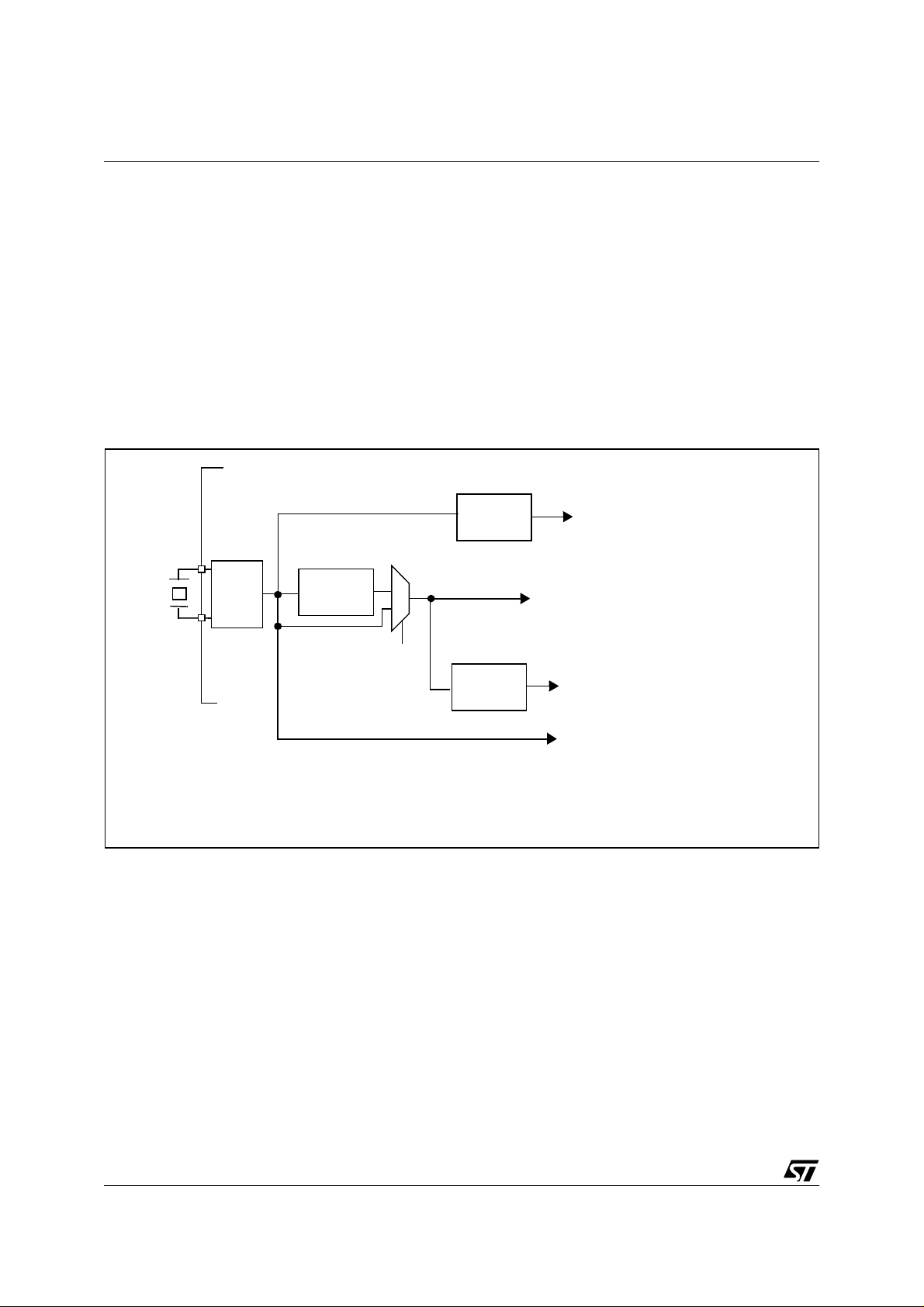
CLOCK SYSTEM (Cont’d)
3.1.2 Crystal Resonator
The internal oscillat or is designed to operate with
an AT-cut parallel resonant quartz crystal
resonator in the frequency range specified for f
osc
The circuit shown in Figure 8 is recommended
when using a crystal, and Table 4, “.
Recommended Crystal Values,” on page 19 lists
the recommended capacitance and feedback
resistance values. The crystal and associated
components should be mounted as close as
possible to the input pins in order to minimize
output distortion and start-up stabilization time.
Figure 8. Crystal/Ceramic Resonator
CRYSTAL CLOCK
OSCIN OSCOUT
C
L1
C
L2
ST72774/ST727754/ST72734
Table 4
.
Legend:
C
OSCIN and OSCOUT (the value includes the
external capacitance tied to the pin plus the
parasitic capacitance of the board and of the
device).
R
the quartz allowed.
Note: The tables are relative t o the quart z crystal
only (not ceramic resonator).
3.1.3 External Clock
An external clock should be appli ed to t he O SCIN
input with the OSCOUT pin not connected as
shown in Figure 9. The Crystal clock specifications
do not apply when using an external clock input.
The equivalent spe cification of the external clock
source should be used.
. Recomm en de d Crystal Values
24 Mhz Unit
R
SMAX
C
L1
C
L2
, CL2 = Maximum total capacitance on pins
L1
= Maximum series parasitic resistance of
SMAX
70 25 20 Ohms
22 47 56 pf
22 47 56 pf
*Recommended for oscillator stability
1M*
Figure 9. External Clock Source Connections
OSCIN
EXTERNAL
CLOCK
OSCOUT
NC
19/144
Page 20

ST72774/ST727754/ST72734
3.2 RESET
The Reset procedure is used to provide an orderly
software start-up or to quit low powe r modes.
Five conditions generate a reset:
■ LVD,
■ watchdog,
■ external pulse at the RESET pin,
■ illegal address,
■ illegal opcode.
A reset causes the reset vector to be fetched from
addresses FFFEh and FFFFh in order to be loaded
into the PC and with program execution starting
from this point.
An internal circuitry provides a 4096 CPU clock
cycle delay from the time that the oscillator
becomes active.
3.2.1 LVD and Watchdog Reset
The Low Voltage Detector (LVD) generates a reset
when V
when
is active only when V
is below V
DD
is falling (refer to Figure 11). This circuitry
VDD
when VDD is ri sing or V
TRH
is above V
DD
TRM.
TRL
During LVD Reset, the RESET pin is held low, thus
permitting the MCU to reset other devices.
When a watchdog reset occurs, the RESET
pin is
pulled low permitting the MCU to reset other
devices as when Power on/off (Figure 10).
3.2.2 External Reset
The external reset is an active low input signal
applied to the RESET pin of the MCU.
As shown in Figure 12, the RESET
signal must
remain low for 1000ns.
An internal Schmitt trigger at the RESET
pin is
provided to improve noise immunity.
3.2.3 Illegal Address Detection
An opcode fetch from an illegal address (refer to
Figure 3) generates an illegal address reset.
Program execution at those addresses is
forbidden (especially to protect page 0 registers
against spurious accesses).
3.2.4 Illegal Opcode Detection
Illegal instructions corresponding to no valid
opcode generate a reset. Refer to ST7
Programming Manual.
Table 5. List of sections affected by RESET and WAIT (Refer to 3.6 for Wait Mo de)
Section RESET WAIT
Fast bit of the miscellaneous register set to one (24 MHz as external clock) X
Timer Prescaler reset to zero X
Timer Counter set to FFFCh X
All Timer enable bits set to 0 (disabled) X
Data Direction Registers set to 0 (as Inputs) X
Set Stack Pointer to 01FFh X
Force Internal Address Bus to restart vector FFFEh, FFFFh X
Set Interrupt Mask Bit (I-Bit, CC) to 1 (Interrupt disable) X
Set Interrupt Mask Bit (I-Bit, CC) to 0 (Interrupt enable) X
Reset WAIT latch X
Disable Oscillator (for 4096 cycles) X
Set Timer Clock to 0 X
Watchdog counter reset X
Watchdog register reset X
Port data registers reset X
Other on-chip peripherals: registers reset X
20/144
Page 21
RESET (Cont’d)
ST72774/ST727754/ST72734
Figure 10. Low Voltage Detector Functional Diagram
V
DD
LVD
RESET
FROM
WATCHDOG
RESET
RESPOF
INTERNAL
RESET
Figure 11. LVD Reset Signal Output
Note: See electrical characteristics section for
values of V
Figure 12. Reset Timing Diagram
t
DDR
V
DD
OSCIN
t
OXOV
V
V
DD
RESET
TRM
V
TRH
TRH, VTRL
and V
TRM
V
TRL
V
TRM
f
CPU
PC
t
RL
RESET
WATCHDOG RESET
Note: Refer to Electrical Characteristics for values of t
4096 CPU
CLOCK
CYCLES
DELAY
, t
OXOV and
DDR
FFFE
t
FFFF
RL
21/144
Page 22

ST72774/ST727754/ST72734
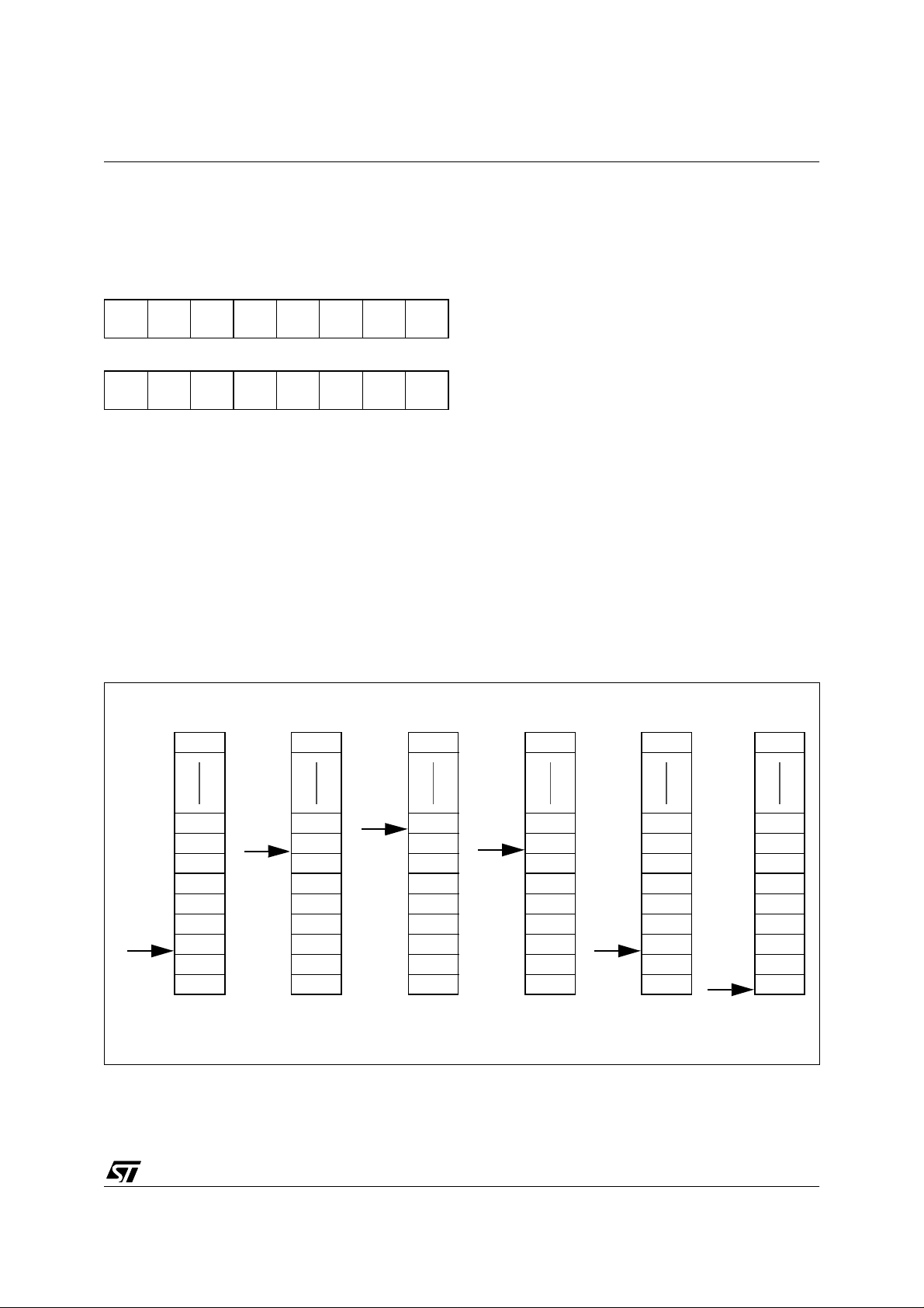
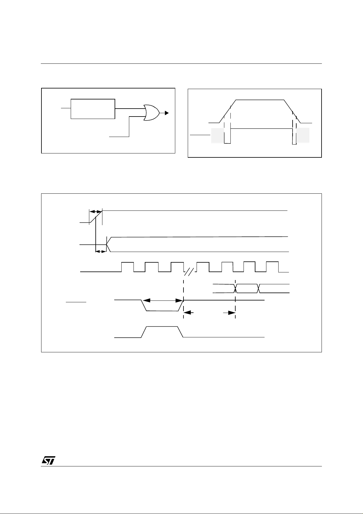
3.3 INTERRUPTS
The ST727x4 may be interrupted by one of two
different methods: maskable hardware interrupts
as listed in T able 6 and a non-maskab le software
interrupt (TRAP). The Interrupt processing
flowchart is shown in Figure 13.
The maskable interrupts must be enabled in order
to be serviced. However, disabled interrupts can
be latched and processed when they are enabled.
When an interrupt has to be serviced, the PC, X, A
and CC registers are saved onto the stack and the
interrupt mask (I bit of the Condition Code
Register) is set to prevent additional interrupts.
The Y register is not automatically saved.
The PC is then load ed with the interrupt vector of
the interrupt to service and the interrupt service
routine runs (refer to Table 6, “Interrupt Mapping,”
on page 24 for vector addresses). The interrupt
service routine should finish with the IRET
instruction which causes the contents of the
registers to be recovered from the stack and
normal processing to resume. Note that the I bit is
then cleared if and only if the corresponding bit
stored in the stack is zero.
Though many interrupts can be simultaneously
pending, a priority order is defined (see Table 6,
“Interrupt Mapping,” on page 24). The RESET
pin
has the highest priority.
If the I bit is set, only the TRAP interrupt is enabled.
All interrupts allow the processor to leave the
WAIT low power mode.
Software Interrupt. The software interrupt is the
executable instruction TRAP. The interrupt is
recognized when the TRAP instruction is
executed, regardless of the state of the I bit. When
the interrupt is recognized, it is serviced according
to the flowchart on Figure 13.
ITA, ITB interrupts. The ITA (PD3), ITB (PD4),
pins can generate an interrupt when a falling edge
occurs on these pins, if these interrupts are
enabled with the ITAITE, ITBITE bits respectively
in the miscellaneous register and the I bit of the CC
register is reset. When an enabled interrupt
occurs, normal processing is suspended at the
end of the current instruct ion execution. It is then
serviced according to the flowchart on Figure 13.
Software in the ITA or ITB service routine must
reset the cause of this interrupt by clearing the
ITALAT, ITBLAT or ITAITE, ITBITE bits in the
miscellaneous register.
Peripheral Interrupts. Different peripheral
interrupt flags are able to cause an interrupt when
they are active if both the I bit of the CC register is
reset and if the corresponding enable bit is set. If
either of these conditions is false , the interrupt is
latched and thus remains pending.
The interrupt flags are located in the status
register. The Enable bits are in the control register.
When an enabled interrupt occurs, normal
processing is suspended at the end of the current
instruction execution. It is then serviced according
to the flowchart on Figure 13.
The general sequence for clearing an interrupt is
an access to the status register while the flag is set
followed by a read or write of an associated
register. Note that the clearing sequence resets
the internal latch. A pending interrupt (i.e. waiting
for being ena b led ) w ill therefore be los t if the clea r
sequence is executed.
22/144
Page 23
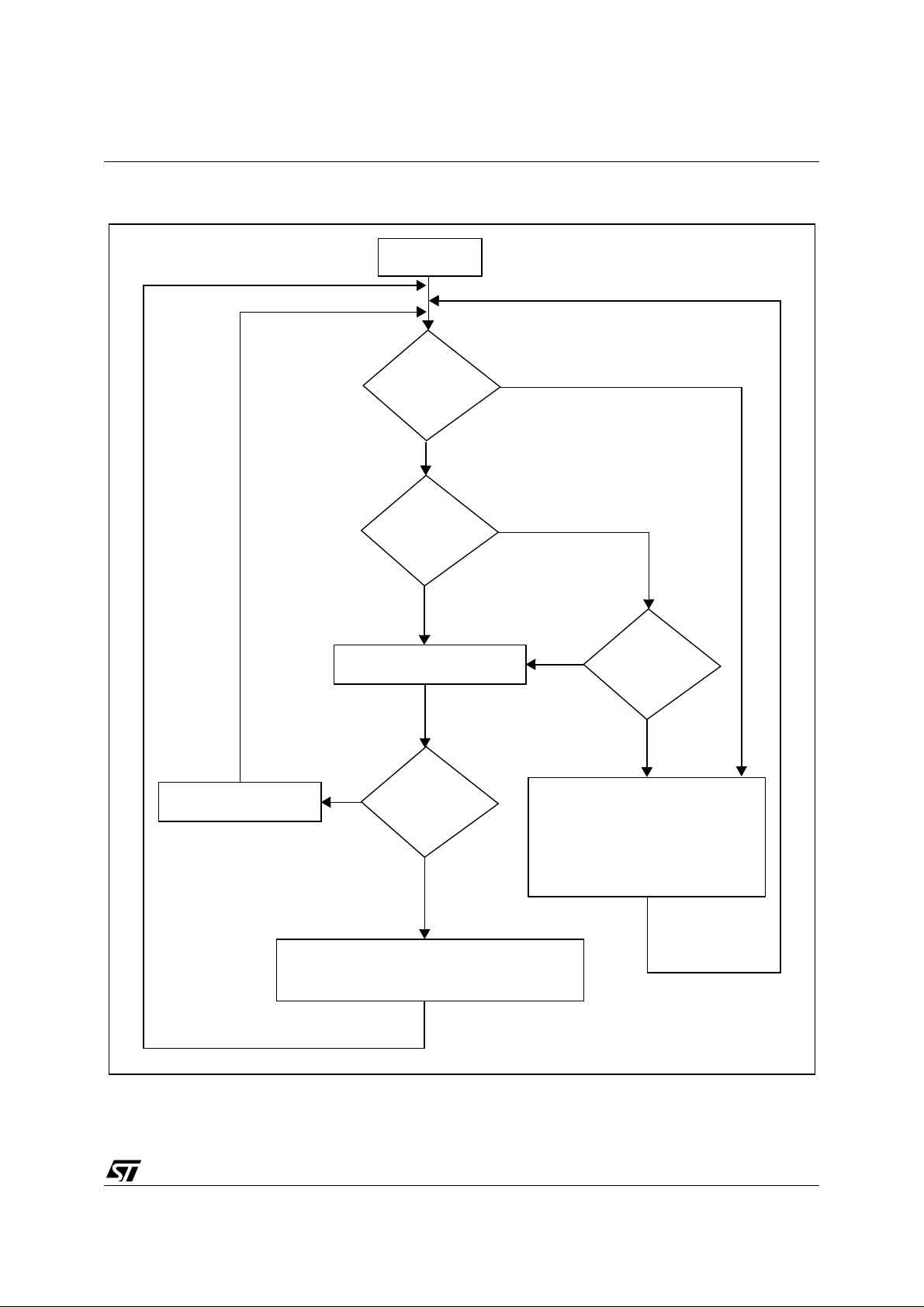
INTERRUPTS (Cont’d)
Figure 13. I nt errupt Processin g Fl owchart
FROM RESET
ST72774/ST727754/ST72734
EXECUTE INSTRUCTION
TRAP?
N
N
I BIT SET?
Y
FETCH NEXT INSTRUCTION
N
IRET?
Y
N
INTERRUPT?
Y
STACK PC, X, A, CC
SET I BIT
LOAD PC FROM INTERRUPT VECTOR
Y
RESTORE PC, X, A, CC FROM STACK
THIS CLEARS I BIT BY DEFAULT
VR01172D
23/144
Page 24
ST72774/ST727754/ST72734
INTERRUPTS (Cont’d)
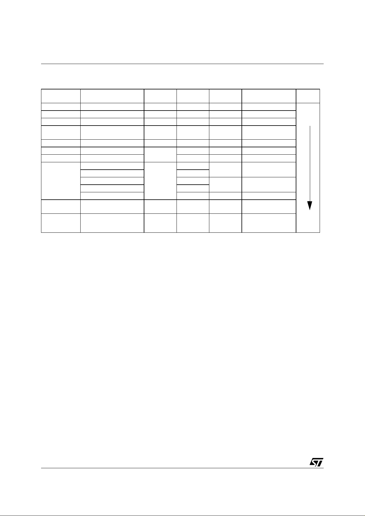
Table 6. Int errupt Mappin g
Source
Block
RESET Reset N/A N/A no FFFEh-FFFFh
TRAP Software N/A N/A no FFFCh-FFFDh
USB End Suspend Interrupt USBISTR ESUSP yes FFFAh-FFFBh
DDC/CI DDC/CI Interrupt
DDC1/2B DDC1/2B Interrupt DDCDCR EDF yes FFF6h-FFF7h
Port D bit 4 External Interrupt ITB
Port D bit 3 External Interrupt ITA ITALAT yes FFF2h-FFF3h
TIM
I2C
USB USB Interrupt USBISTR ** yes FFE6h-FFE7h
Description
Input Capture 1
Input Capture 2 ICF2
Output Compare 1 OCF1
Output Compare 2 OCF2
Timer Overflow TOF yes FFECh-FFEDh
I2C Peripheral Inter-
rupts
Register
Label
DDCSR1
DDCSR2
MISCR
TIMSR
I2CSR1
I2CSR2
Flag
** yes FFF8h-FFF9h
ITBLAT yes FFF4h-FFF5h
ICF1
** yes FFEAh-FFEBh
Maskable
by I-bit
yes FFF0h-FFF1h
yes FFEEh-FFEFh
Vector Address
Priority
Order
Highest
Priority
Lowest
Priority
** Many flags can cause an interrupt, see peripheral interrupt status register description.
24/144
Page 25
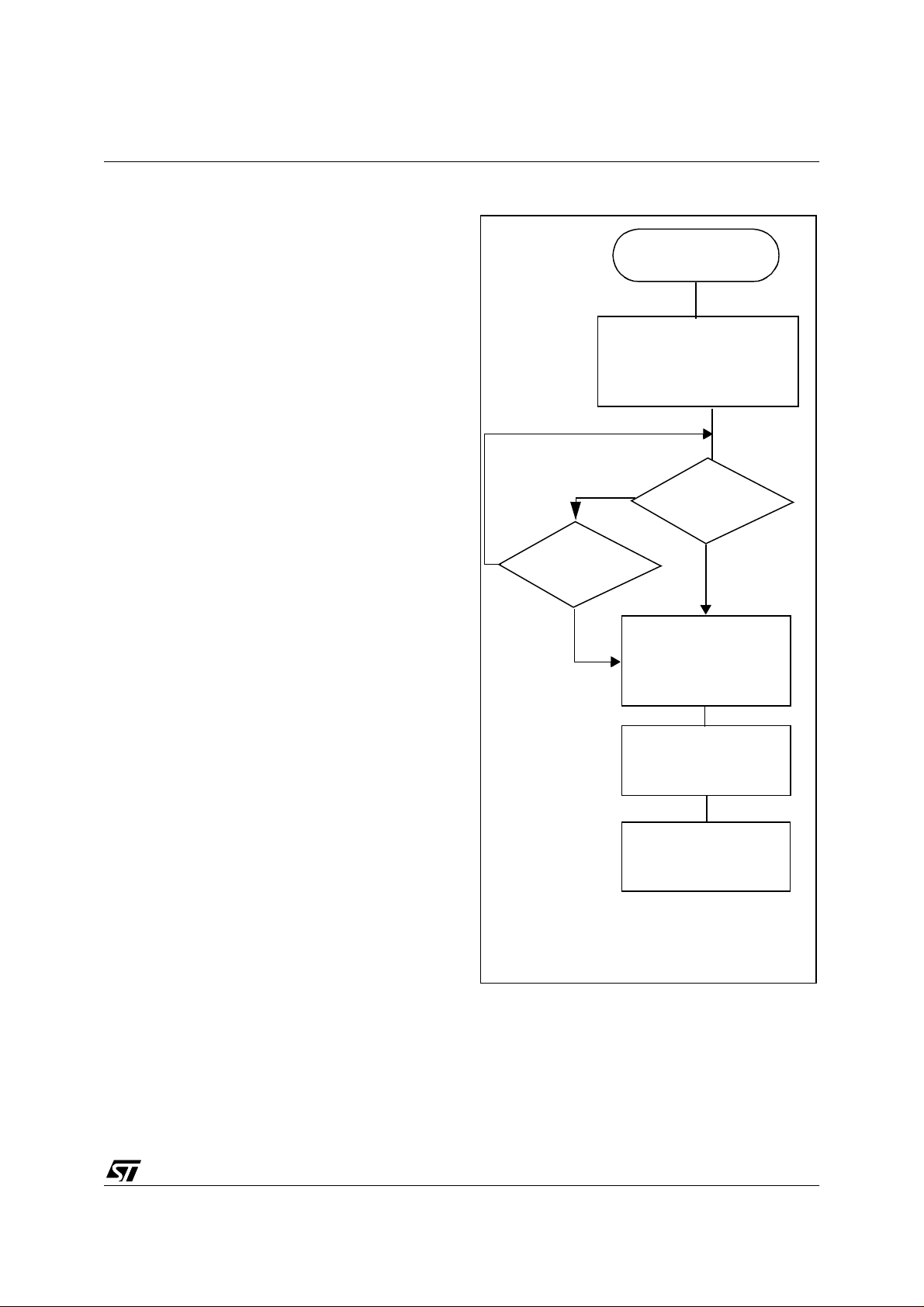
3.4 POWER SAVI NG MO DE S
ST72774/ST727754/ST72734
3.4.1 WAIT Mode
This mode is a low power consumption mode. The
WFI instruction places the MCU in WAIT mode:
The internal clock remains active but all CPU
processing is stopped; however, all other
peripherals are still running.
Note: In WAIT mode, DMA accesses (DDC, USB)
are possible.
During WAIT mode, the I bit in the condition code
register is cleared to enable all interrupts, whi ch
causes the MCU to exit WAIT mode, causes the
corresponding interrupt vector to be fetched, th e
interrupt routine to be executed and normal
processing to resume. A reset causes the program
counter to fetch the reset vector and processing
starts as for a normal reset.
Table 5 gives a list of the different sections
affected by the low power modes. For detailed
information on a particular device, please refer to
the corresponding part.
Figure 14. WAIT Flow Chart
WFI INSTRUCTION
OSCILLATOR
PERIPH. CLOCK
CPU CLOCK
I-BIT
N
N
INTERRUPT
Y
OSCILLATOR
PERIPH. CLOCK
CPU CLOCK
I-BIT
ON
ON
OFF
CLEARED
RESET
Y
ON
ON
ON
SET
3.4.2 HALT Mode
The HALT mode is the MCU lowest power
consumption mode. Meanwhile, the HALT mode
also stops the oscillator stage comple tely which is
the most critical condition in CRT monitors.
For this reason, the HALT mode has been disabled
and its associated HALT instruction is now
considered as illegal and will generate a reset.
IF RESET
4096 CPU CLOCK
CYCLES DELAY
FETCH RESET VECTOR
OR SERVICE INTERRUPT
Note: Before servicing an interrupt, the CC register is
pushed on the sta ck. T he I-Bit is s et d uring the inte rrupt routine and cleared when the CC register is
popped.
25/144
Page 26

ST72774/ST727754/ST72734
3.5 MISCELLANEOUS REGISTER
MISCELLANEOUS REGISTER (MISCR)
Address: 0009h — R ea d/W rite
Reset Value: 0001 0000 (10h)
70
VSYNC
FLY_SYNHSYNC
SEL
FAST ITBLAT ITALAT ITBITE ITAITE
DIVEN
Bit 4= FAST
Fast Mode.
This bit is set and cleared by software. It is used to
select the external cloc k frequ ency . If th e exte rnal
clock frequency is 12 M Hz, this bit must be at 0,
else if the external frequency is 24 MHz, this bit
must be at 1.
Bit 7= VSYNCSEL
DDC1 VSYNC Selection.
This bit is set and cleared by software. It is used to
choose the VSYNC signal in DDC1 mode.
0: VSYNCI selected
1: VSYNCI2 selected
Note: VSYNCI 2 is only available for the DDC cell,
not for the SYNC processor cell.
Bit 6= FL Y _SY N
Flyback or Synchro Switch.
This bit is set and cleared by software. It is used to
choose the signals the Timing Measureme nt Unit
(TMU) will analyse.
0: horizontal and vertical synchro outputs analysis
1: horizontal and vertical Flyback inputs analysis
Bit 5= HS YNCDIVEN
HSYNCDIV Enable.
This bit is set and cleared by software. It is used to
enable the output of the HSYNCO output on PC0.
0: HSYNCDIV disabled
1:HSYNCDIV enabled
Bit 3= ITBLAT
Falling Edge Detector Latch.
This bit is set by hardware when a falling edge
occurs on pin ITB/PD4 in Port D. An interrupt is
generated if ITBITE=1and the I bit in the CC
register = 0. It is cleared by software.
0: No falling edge detected on ITB
1: Falling edge detected on ITB
Bit 2= ITALAT
Falling Edge Detector Latch.
This bit is set by hardware when a falling edge
occurs on pin ITA/PD3 in Port D. An interrupt is
generated if ITAITE=1and the I bit in the CC
register = 0. It is cleared by software.
0: No falling edge detected on ITA
1: Falling edge detected on ITA
Bit 1= ITBITE
ITB Interrupt Enable
.
This bit is set and cleared by software.
0: ITB interrupt disabled
1: ITB interrupt enabled
Bit 0= ITAITE
ITA Interrupt Enable
.
This bit is set and cleared by software.
26/144
0: ITA interrupt disabled
1: ITA interrupt enabled
Page 27
4 ON-CHIP PERIPHERALS
4.1 I/O PORTS
ST72774/ST727754/ST72734
4.1.1 Introd uct i on
The I/O ports allow the transfer of data through
digital inputs and outputs, and, for specific pins,
the input of analog s ignals or the Input/Output of
alternate signals for on-chip peripherals (DDC,
TIMER...).
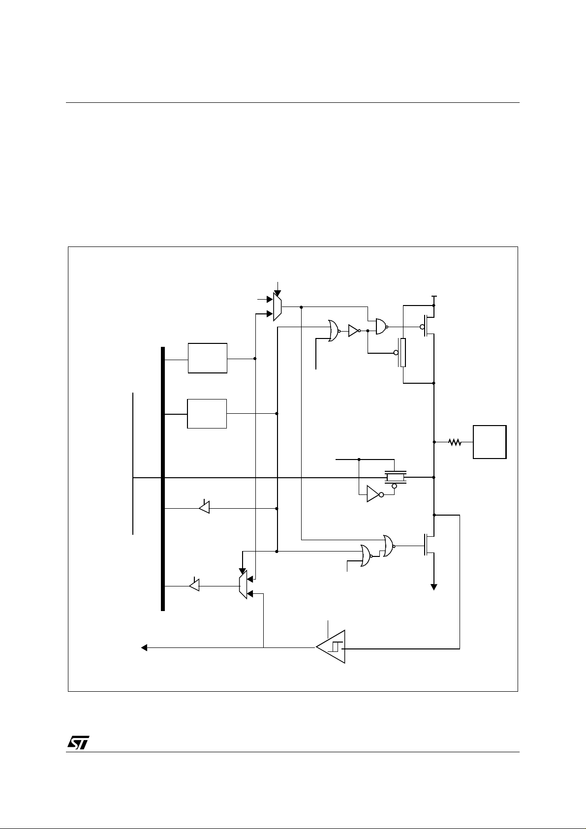
Figure 15. I/O Pin Typical Cir cuit
Alternate enable
Alternate
1
output
0
DR
latch
Data Bus
DDR
latch
Each pin can be programmed independently as
digital input or digital output. E ach pin can be an
analog input when an analog switch is connected
to the Analog to Digital Converter (ADC).
V
DD
P-BUFFER
(if required)
PULL-UP (if required)
Alternate enable
PAD
Analog Enable
(ADC)
Common Analog Rail
DDR SEL
Analog
Switch (if required)
N-BUFFER
DR SEL
1
Alternate Enable
0
Digital Enable
V
SS
Alternate Input
Note: This is the typical I/O pin configuration. For cost optimization, each port is customized with a specific configuration.
27/144
5
Page 28

ST72774/ST727754/ST72734
I/O PORTS (Cont’d)
Table 7. I/O Pin Functions
DDR MODE
0 Input
1 Output
4.1.2 Common Functional Description
Each port pin of the I/O Ports can be individual ly
configured under software control as either i nput
or output.
Each bit of a Data Direction Register (DDR)
corresponds to an I/O pin of the associated p ort.
This corresponding bit must be set to configure its
associated pin as output and must be cleared to
configure its associated pin as input (Table 7, “. I/O
Pin Functions,” on page 28). The Data Direction
Registers can be read and written.
The typical I/O circuit is shown on Figure 15. Any
write to an I/O port updates the port data register
even if it is configured as input. Any read of an I/O
port returns either the data latched in the port data
register (pins configured as output) or the value of
the I/O pins (pins configured as input).
Remark: when an I/O pin does not exist inside an
I/O port, the returned value is a logic one (pin
configured as input).
At reset, all DDR registers are cleared, which
configures all port’s I/Os as inputs with or without
pull-ups (see Table 8 to Table 12 I/O Ports
Register Map). The Data Registers (DR) are also
initialized at reset.
4.1.2.1 Input mode
When DDR=0, the corresponding I/O is configured
in Input mode.
In this case, the output buffer is switched off, the
state of the I/O is readable through the Data
Register address, but the I/O state comes directly
from the CMOS Schmitt Trigger output and not
from the Data Register output.
4.1.2.2 Output mode
When DDR=1, the corresponding I/O is configured
in Output mode.
In this case, the output buffer is activated
according to the Data Register’s content.
A read operation is directly performed from the
Data Register output.
4.1.2.3 Analog input
Each I/O can be used as analog input by adding an
analog switch driven by the ADC.
The I/O must be configured in Input before using it
as analog input.
The CMOS Schmitt trigger is OFF and the analog
value directly input through an analog switch to the
Analog to Digital Converter, when the analog
channel is selected by the ADC.
4.1.2.4 Alternate mode
A signal coming from a on-chip peripheral can be
output on the I/O.
In this case, the I/O is automaticall y configured in
output mode.
This must be controlled directly by the peripheral
with a signal coming from the peripheral which
enables the alternate signal to be output.
A signal coming from an I/O can be inpu t in a onchip peripheral.
Before using an I/O as Alternate Input, it must be
configured in Input mode (DDR=0). So both
Alternate Input configuration and I/O Input
configuration are the same (with or without pullup). The signal to be input in the peripheral is taken
after the CMOS Schmitt trigger or TTL Schmitt
trigger for SYNC.
The I/O state is readable as in Input mode by
addressing the corresponding I/O Data Register.
28/144
Page 29
ST72774/ST727754/ST72734
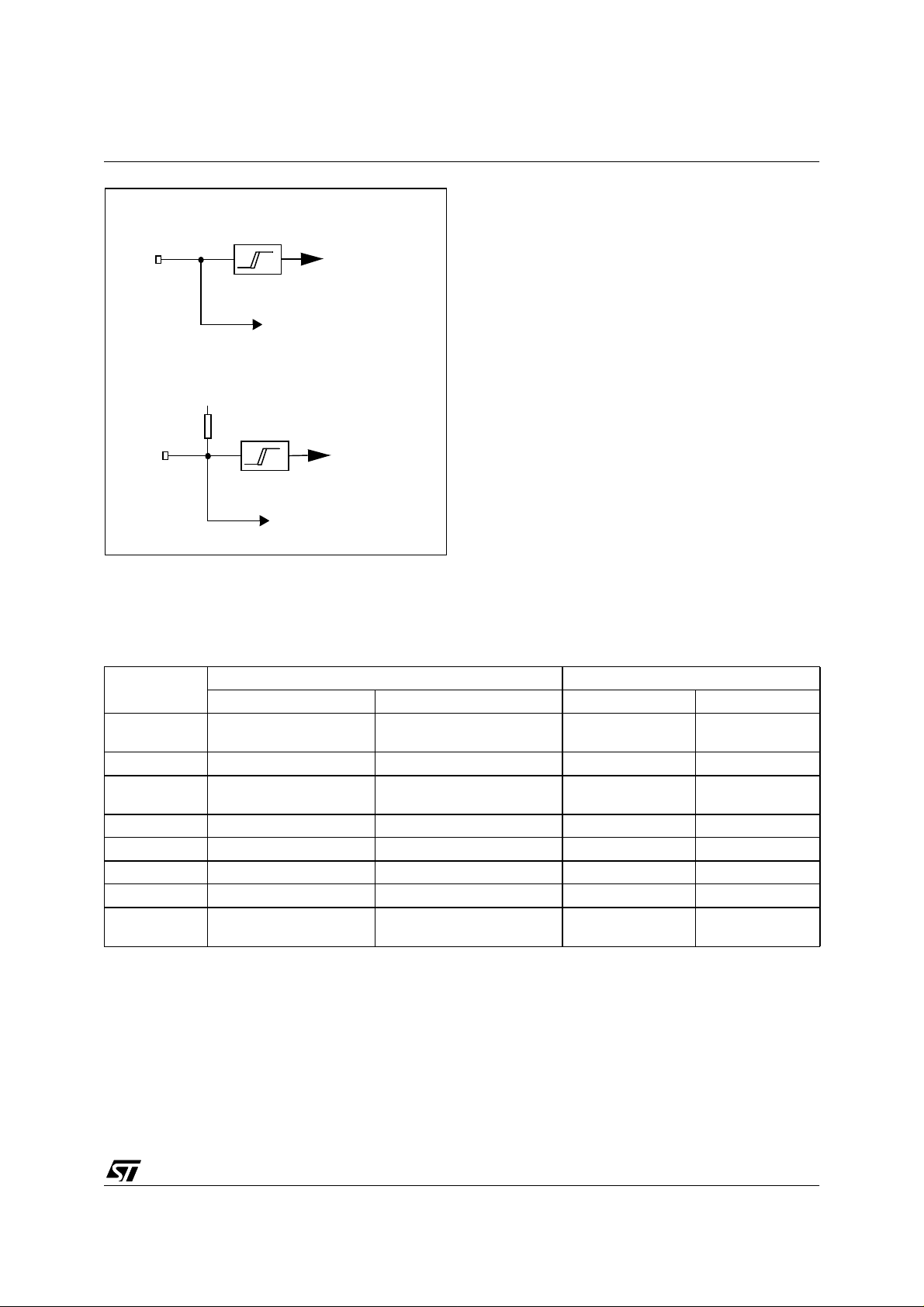
Figure 16. Input Structure for SYNC signals
TTL trigger
Pin
HSYNCI Input
VSYNCI Input
(no pull-up)
I/O logic (if existing)
V
DD
TTL trigg erpull-up
CSYNCI Input
Pin
HFBACK Input
VFBACK Input
I/O logic (if existing)
4.1.3 Port A
PA7 and PA[2:0] can be defined as Input lines
(with pull-up) or as Push-pull Outputs.
PA [6:3] can be defined as Input lines (without pullup) or as Output Open drain lines.
PA7 and PA[2:0] can be defined as Input lines
(with pull-up) or as Push-pull Outputs.
PA [6:3] can be defined as Input lines (without pullup) or as Output Open drain lines.
Table 8. Port A Description
PORT A
PA0 With pull-up push-pull OCMP1
PA1 With pull-up push-pull - PA2 With pull-up push-pull VSYNCI2
PA3 Without pull-up open-drain - -
PA4 Without pull-up open-drain - PA5 Without pull-up open-drain - PA6 Without pull-up open-drain - -
PA7 With pull-up push-pull BLANKOUT
*Reset State
Input* Output Signal Condition
I / O Alternate Function
OC1E =1
(CR2[TIMER])
VSYNCSEL=1
(MISCR)
BLKEN = 1
(ENR[SYNC])
29/144
Page 30
ST72774/ST727754/ST72734
I/O PORTS (Cont’d)
Figure 17. PA0 to PA2, PA7
Alternate
output
Alternate enable
1
V
DD
DATA BUS
Figure 18. PA3 to PA6
DR
latch
DDR
latch
DDR SEL
DR SEL
DR
latch
DDR
latch
0
PULL-UP
OC1E
P-BUFFER
N-BUFFER
PAD
1
OC1E
V
SS
0
CMOS Schmitt Trigger
Alternate enable
Alternate
output
1
0
PAD
30/144
DATA BUS
Alternate input
DDR SEL
DR SEL
N-BUFFER
1
0
Alternate enable
CMOS Schmitt Trigger
V
SS
Page 31

ST72774/ST727754/ST72734
I/O PORTS (Cont’d)
4.1.4 Port B
The alternate functions are the I/O pins of the onchip DDC SCLD & SCDAD for PB0:1, the I/O pins
of the on-chip I2C SCLI & SCDAI for PB2:3, and 4
bits of port B bit can be used as the Analog source
to the Analog to Digital Converter.
Only one I/O line must be configured as an analog
input at any time. The user must avoid any
situation in which more than one I/O pin is selected
as an analog input simultaneously to av oid de vice
malfunction.
When the analog function is selected for an I/O pin,
the pull-up of the respective pin of Port B is
disconnected and the digital input is off.
Table 9. Port B Description
PORT B I/O Alternate Function
Input* Output Signal Condition
All unused I/O lines should be tied to an
appropriate logic level (either V
Since the ADC is on the same chip as the
microprocessor, the user should not switch heavily
loaded signals during conversion, if high precision
is required. S uch switching will affec t the supply
voltages used as analog references . the a ccuracy
of the conversion depends on the quality of the
power supplies (V
and VSS). The user must take
DD
special care to ensure that a well regulated
reference voltage is present on the V
pins (power supply variations must be less than
5V/ms). T his impli es, in particul ar, that a su itable
decoupling capacitor is used at the V
or VSS)
DD
DD
DD
and V
pin.
SS
PB0 Without pull-up Open-drain
PB1 Without pull-up Open-drain
PB2 Without pull-up Open-drain
PB3 Without pull-up Open-drain
PB4 With pull-up Push-pull Analog input (ADC) (without pull-up) CH[2:0]=000 (ADCCSR)
PB5 With pull-up Push-pull Analog input (ADC) (without pull-up) CH[2:0]=001 (ADCCSR)
PB6 With pull-up Push-pull
PB7 With pull-up Push-pull
*Reset state
SCLD (input with CMOS schmitt trigger or
open drain output)
SDAD (input with CMOS schmitt trigger or
open drain output)
SCLI (input with CMOS schmitt trigger or
open drain output)
SDAI (input with CMOS schmitt trigger or
open drain output)
Analog input (ADC) (without pull-up) CH[2:0]=010 (ADCCSR)
10-bit output 1 (PWM) OE0=1 (PWMOE)
Analog input (ADC) (without pull-up) CH[2:0]=011 (ADCCSR)
10-bit output 2 (PWM) OE1=1 (PWMOE)
DDC enable
DDC enable
I2C enable
I2C enable
31/144
Page 32

ST72774/ST727754/ST72734
I/O PORTS (Cont’d)
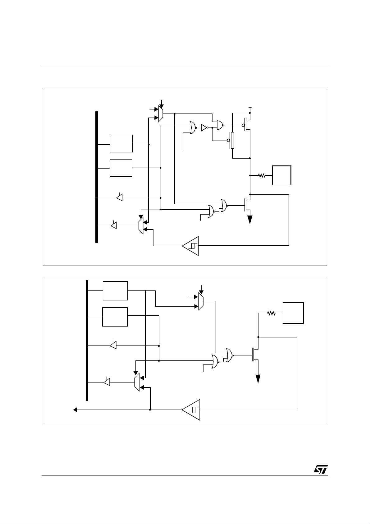
Figure 19. PB0 to PB3
DR
latch
DDR
latch
DDR SEL
Alternate
output
Alternate enable
1
0
PAD
N-BUFFER
DATA BUS
DR SEL
Alternate input
Figure 20. PB4 to PB7
DATA BUS
Common Analog Rail
DR
latch
DDR
latch
DDR SEL
1
0
CMOS Schmitt Trigger
Alternate enable
Analog enable
(ADC)
V
PULL-UP
Analog
switch
SS
V
DD
P-BUFFER
PAD
32/144
DR SEL
DR SEL
N-BUFFER
1
1
V
0
0
CMOS Schmitt Trigger
SS
Page 33

I/O PORTS (Cont’d)
4.1.5 Port C
The available port pins of port C may be used as
general purpose I/O.
Table 10. Port C Description
ST72774/ST727754/ST72734
The alternate functions are the PWM outputs for
PC2:7, HSYNCDIV (HSYNCO divided by 2) for
PC0 and the TMU input for PC1.
PORT C
PC0 With pull-up Push-pull HSYNCDIV (push-pull)
PC1 With pull-up Push-pull AV (active video) input (TMU) PC2 With pull-up Push-pull 10-bit output 3 (PWM)
PC3 With pull-up Push-pull 10-bit output 4 (PWM)
PC4 With pull-up Push-pull 10-bit output 5 (PWM)
PC5 With pull-up Push-pull 10-bit output 6 (PWM)
PC6 With pull-up Push-pull 10-bit output 7 (PWM)
PC7 With pull-up Push-pull 10-bit output 8 (PWM)
* Reset State
I / O Alternate Function
Input* Output Signal Condition
HSYNCDIVEN
=1
(MISCR)
OE2=1
(PWMOE)
OE3=1
(PWMOE)
OE4=1
(PWMOE)
OE5=1
(PWMOE)
OE6=1
(PWMOE)
OE7=1
(PWMOE)
33/144
Page 34

ST72774/ST727754/ST72734
I/O PORTS (Cont’d)
Figure 21. PC0, PC2 to PC7
Alternate
output
Alternate enable
1
V
DD
Figure 22. PC1
DATA BUS
DR
latch
DDR
latch
DDR SEL
DR SEL
DR
latch
0
PULL-UP
OC1E
1
0
OC1E
CMOS Schmitt Trigger
P-BUFFER
N-BUFFER
V
SS
P-BUFFER
PAD
V
DD
34/144
AV
DDR
latch
DDR SEL
DATA BUS
DR SEL
1
0
CMOS Schmitt Trigger
PULL-UP
V
SS
PAD
N-BUFFER
Page 35

I/O PORTS (Cont’d)
4.1.6 Port D
The Port D I/O pins are normally used for the input
and output of video synchronization signals of the
Sync Processor, but are set to I/O Input with pullup upon reset. The I/O mode can be set
individually for each port bit to Input with pull-up
and output push-pull through the Port D DDR.
The configuration to supp ort the Sync Processor
requires that the SYNOP (bit7) and CLMPEN (bit6)
of the ENR (Enable Register of SYNC) is reset.
SYNOP enables port D bits 0,1 and CLMPEN
enables Port D bit 6 to the sync outputs.
Port D, bit 4:3 are the alternate inputs ITA, ITB, (for
the interrupt falling edge detector).
When a falling edge occurs on these inputs, an
interrupt will be generated depending on the status
of the INTX (ITAITE & ITBITE) bit s in the MISCR
Register.
Table 11. Port D Description
ST72774/ST727754/ST72734
Port D, bit 6 is switched to the alternate
(CLAMPOUT) by reset ting the CLMPEN bit of the
ENR Register inside SYNC block.
If the SYNC function is selected, Port D bit 5 and 3
MUST be set as input to enable the HFBACK or
VFBACK timin g in p uts.
Note: As these inputs are switched from normal
I/O function ality, the v ideo sync hronization signals
may also be mo nitored dire ctly through the Port D
Data Register for such tasks as checking for the
presence of video signals or checking the polarity of
Horizontal and Vertical synchronization signals
(when the Syn c Inputs are s witched dire ctly to the
outputs usin g the m ultip lexers of the Sync Proc essor).
PORT D
PD0 With pull-up Push-pull
PD1 With pull-up Push-pull
PD2 With pull-up Push-pull
PD3 With pull-up Push-pull
PD4 With pull-up Push-pull
PD5 With pull-up Push-pull
PD6 With pull-up Push-pull
* Reset state
Input* Output Signal Condition
I / O Alternate Function
VSYNCO
(push pull output)
HSYNCO
(push pull output)
CSYNCI (input with TTL Schmitt
trigger & pull-up)
ITA (input with CMOS Schmitt
trigger & pull-up)
VFBACK (input with TTL Schmitt
trigger & pull-up)
ITB (input with CMOS Schmitt
trigger & pull-up)
HFBACK (input with TTL Schmitt
trigger & pull-up)
CLAMPOUT
(push pull output)
SYNOP=0
(ENR [SYNC])
SYNOP=0
(ENR [SYNC])
-
-
-
-
CLMPEN=0
(ENR [SYNC])
35/144
Page 36

ST72774/ST727754/ST72734
I/O PORTS (Cont’d)
Figure 23. PD2 to PD5
DR
DATA BUS
latch
DDR
latch
DDR SEL
PULL-UP
V
DD
P-BUFFER
PAD
N-BUFFER
CSYNCI Input
HFBACK Input
VFBACK Input
Figure 24. PD0 to PD1
DATA BUS
DR SEL
alternate input
Alternate
output
DR
latch
DDR
latch
DDR SEL
1
0
CMOS Schmitt Trigger
TTL Schmitt Trigger
Alternate enable
1
0
Alternate enable
V
SS
VDD
PULL-UP
P-BUFFER
PAD
36/144
Alternate input
DR SEL
N-BUFFER
1
0
Alternate enable
CMOS Schmitt Trigger
V
SS
Page 37

I/O PORTS (Cont’d)
Figure 25. PD6
Alternate
output
ST72774/ST727754/ST72734
Alternate enable
1
0
VDD
P-BUFFER
Alternate input
VSYNCI2 input
DATA BUS
DR
latch
DDR
latch
DDR SEL
DR SEL
PULL-UP
Alternate enable
PAD
N-BUFFER
1
0
Alternate enable
CMOS Schmitt Trigger
TTL Schmitt Trigger
V
SS
37/144
Page 38

ST72774/ST727754/ST72734
I/O PORTS (Cont’d)
4.1.7 Register Description
Data Registers (PxDR)
Read/Write
Reset Value: 0000 0000 (00h)
70
MSB LSB
Table 12. I/O Ports Register Map
Data Direction Registers (PxDDR)
Read/Write
Reset Value: 0000 0000 (00h) (as inputs)
70
MSB LSB
Address
(Hex.)
00 PADR MSB LSB
01 PADDR MSB LSB
02 PBDR MSB LSB
03 PBDDR MSB LSB
04 PCDR MSB LSB
05 PCDDR MSB LSB
06 PDDR MSB LSB
07 PDDDR MSB LSB
Register
Name
76543210
38/144
Page 39

4.2 WATCHDOG TIMER (WDG)
ST72774/ST727754/ST72734
4.2.1 Introd uct i on
The Watchdog timer is used to detect the
occurrence of a software fault, usually generated
by external interference o r by unforeseen logical
conditions, which causes the applicatio n program
to abandon its normal sequence. The Watchdog
circuit generates an MCU reset on expiry of a
programmed time period, unless the program
Figure 26. Watchdog Block Diagram
RESET
WATCHDOG CONTROL REGISTER (CR)
T5
WDGA
T6 T0
T4
refreshes the counter’s cont ents before t he T6 bit
becomes cleared.
4.2.2 Main Features
■ Programmable timer (64 increments of 49152
CPU cycles)
■ Programmable reset
■ Res et (if watchdog activated) when the T6 bit
reaches zero
T1
T2
T3
7-BIT DOWNCOU NTE R
f
CPU
CLOCK DIVIDER
49152
÷
4.2.3 Functional Description
The counter value stored in the CR register (bits
T6:T0), is decremented every 49,152 machine
cycles, and the length of the timeout period can be
programmed by the user in 64 increments.
If the watchdog is activated (the W DGA bit is s et)
and when the 7-bit timer (bits T6:T0) rolls over
from 40h to 3Fh (T6 becomes cleared), it initiates a
reset cycle pulling low the reset pin for typically
500ns.
The application program must write in the CR
register at regular intervals during normal
operation to prevent an MCU reset. Th e value to
be stored in the CR register must be between FFh
and C0h (see Table 13 . Watchdog Timing (fCPU =
8 MHz)):
– The WDGA bit is set (watchdog enabled)
– The T6 bit is set to prevent generating an imme-
diate reset
– The T5:T0 bits contain the number of increments
which represents the time delay before the
watchdog produces a reset.
39/144
Page 40

ST72774/ST727754/ST72734
Table 13. Watchdog Timing (f
CR Register
initial value
Max FFh 393.216
Min C0h 6.144
= 8 MHz)
CPU
WDG timeout period
(ms)
Notes: Following a reset, the watchdog is
disabled. Once activated it cannot be disabled,
except by a reset.
The T6 bit can be used to generate a software
reset (the WDGA bit is set and the T6 bit is
cleared).
4.2.4 Interrupts
None.
4.2.5 Register Description
CONTROL REGISTER (CR)
Read/Write
Reset Value: 0111 1111 (7Fh)
70
WDGA T6 T5 T4 T3 T2 T1 T0
Bit 7 = WDGA
Activation bit
.
This bit is set by software and only cleared by
hardware after a reset. When WDGA = 1, the
watchdog can generate a reset.
0: Watchdog disabled
1: Watchdog enabled
Bit 6:0 = T[6:0]
7-bit timer (MSB to LSB).
These bits contain the decremented value. A reset
is produced when it rolls over from 40h to 3Fh (T6
becomes cleared).
Table 14. Watchdog Time r Register Map and Rese t Values
Address
(Hex.)
08
40/144
Register
Label
WDGCR
Reset Value
76543210
WDGA
0
T6
T5
1
1
T4
1
T3
T2
1
1
T1
T0
1
1
Page 41

4.3 16-BIT TIMER (TIM)
ST72774/ST727754/ST72734
4.3.1 Introd uct i on
The timer consists of a 16-bit free-running counter
driven by a programmable prescaler.
It may be used for a variety of purposes, including
pulse length measurement of up to two input
signals (
output waveforms (
input capture
output compare
) or generation of up to two
and
PWM
).
Pulse lengths and waveform periods can be
modulated from a few microseconds to several
milliseconds using the timer prescaler and the
CPU clock prescaler.
4.3.2 Main Features
■ Programmable prescaler: f
divided by 2, 4 or
cpu
8.
■ Overflow status flag and maskable interrupt
■ External clock inpu t (must be at least 4 times
slower than the CPU
clock speed) with the
choice of active edge
■ Output compare functions with
– 2 dedicated 16-bit registers
– 2 dedicated programmable signals
– 2 dedicated status flags
– 1 dedicated maskable interrupt
■ Input capture functions with
– 2 dedicated 16-bit registers
– 2 dedicated active edge selection signals
– 2 dedicated status flags
– 1 dedicated maskable interrupt
■ Pulse width modulation mode (PWM)
■ One pulse mode
■ 5 alternate functions on I/O ports*
4.3.3 Functional Description
4.3.3.1 Counter
The principal block of the Programmable Timer is a
16-bit free running counter and its associated 16bit registers:
Counter Registers
– Counter High Register (CHR) is the most sig-
nificant byte (MSB).
– Counter Low Register (CLR) is the least sig-
nificant byte (LSB).
Alternate Counter Registers
– Alternate Count er Hi gh Regi ster ( ACHR) is th e
most significant byte (MSB).
– Alternate Counter Low Register (ACLR) is the
least significant byt e (LSB).
These two read-only 16-bit registers contain the
same value but with the difference that reading the
ACLR register does not clear the TOF bit (overflow
flag), (see note page 43).
Writing in the CLR register or ACLR register resets
the free running counter to the FFFCh value.
The timer clock depends on the cloc k control bits
of the CR2 register, as illustrated in Table 15 Clock
Control Bits. The value in the counter register
repeats every 131.072, 262.144 or 524.288
internal processor clock cycles depending on the
CC1 and CC0 bits.
The Block Diagram is shown in Figure 27.
Note: Some external pins are not available on all devices.
Refer to the device pin out description.
41/144
Page 42

ST72774/ST727754/ST72734
16-BIT TIMER (Cont’d)
Figure 27. Timer Block Diagram
ST7 INTERNAL BUS
CPU CLO CK
CC1 CC0
EXTCLK
8 high
EXEDG
1/2
1/4
1/8
8 low
8-bit
buffer
16
16 BIT
FREE RUNNING
COUNTER
COUNTER
ALTERNATE
REGISTER
16
OVERFLOW
DETECT
CIRCUIT
MCU-PERIPHERAL INTERFACE
8
88 8
low
high
OUTPUT
COMPARE
REGISTER
1
low
high
OUTPUT
COMPARE
REGISTER
2
TIMER INTERNAL BUS
16 16
OUTPUT COMPARE
CIRCUIT
8
low
high
INPUT
CAPTURE
REGISTER
1
EDGE DETECT
8 8 8
low
high
INPUT
CAPTURE
REGISTER
2
16
CIRCUIT1
16
ICAP1
42/144
ICF2ICF1 000OCF2OCF1 TOF
TIMER INTERRUPT
SR
CR1
6
EDGE DETECT
ICAP2
CIRCUIT2
OCMP1
OCMP2
EXEDG
OC2E
LATCH1
LAT CH2
PWMOC1E
OPMFOLV2IC IE OLVL1IEDG1OL VL2FOLV1OCIETOIE
IEDG2CC0CC1
CR2
Page 43

16-BIT TIMER (Cont’d)
16-bit read sequence: (from either the Counter
Register or the Alternate Counter Register).
Beginning of the sequence
At t0
Read MSB
LSB is buffered
Other
instructions
Returns the buffered
LSB value at t0
At t0 +Dt
Read LSB
Sequence completed
ST72774/ST727754/ST72734
Clearing the overflow interrupt request is done by:
1. Reading the SR register while the TOF bit is
set.
2. An access (read or write) to the CLR register.
Notes: The TOF bit is not cleared by ac ces ses to
ACLR register. This feature allows simultaneous
use of the overflow f unction and rea ds of t he free
running counter at random times (for example, to
measure elapsed time) without the risk of clearing
the TOF bit erroneously.
The timer is not affected by WAIT mode.
The user must read the MSB first, then the LSB
value is buffered automatically.
This buffered value rem ains unchanged until the
16-bit read sequence is completed, even if the
user reads the MSB several times.
After a complete reading sequence, if only the CLR
register or ACLR register are read, they return the
LSB of the count value at the time of the read.
An overflow occurs when the counter rolls over
from FFFFh to 0000h then:
– The TOF bit of the SR register is set.
– A timer interrupt is generated if:
– TOIE bit of the CR1register is set and
– I bit of the CC register is clea red.
If one of these conditions is false, the interrupt
remains pending to be issued as soon as they are
both true.
4.3.3.2 External Clock
The external clock (wh ere available) is selected if
CC0=1 and CC1=1 in CR2 register.
The status of the EXEDG bit determi nes the type
of level transition on the external clock pin
EXTCLK that will trigger the free running c ounter .
The counter is synchronised with t he falling edge
of the internal CPU clock.
At least four falling edges of the CPU clock must
occur between two consecutive active edges of
the external clock; thus the external clock
frequency must be less than a qu arter of t he CPU
clock frequency.
43/144
Page 44

ST72774/ST727754/ST72734
16-BIT TIMER (Cont’d)
Figure 28. Counter Timing Diagram, internal clock divided by 2
CPU CLOCK
INTERNAL RESET
TIMER CLOCK
COUNTER REGISTER
OVERFLOW FLAG TOF
FFFD FFFE FFFF 0000 0001 0002 0003
Figure 29. Counter Timing Diagram, internal clock divided by 4
CPU CLOCK
INTERNAL RESET
TIMER CLOCK
COUNTER REGI STER
OVERFLOW FLAG TOF
FFFC FFFD 0000 0001
Figure 30. Counter Timing Diagram, internal clock divided by 8
44/144
CPU CLOCK
INTERNAL RESET
TIMER CLOCK
COUNTER REGISTER
OVERFLOW FLAG TOF
FFFC FFFD
0000
Page 45

16-BIT TIMER (Cont’d)
4.3.3.3 Input Capture
In this section, the index,
i
, may be 1 or 2.
The two input capture 16-bit registers (IC1R and
IC2R) are used to latch the value of the free
running counter after a transition detected by the
ICAP
i
pin (see figure 5).
MS Byte LS Byte
i
RIC
IC
i
Rregister is a read-only register.
IC
i
HR ICiLR
ST72774/ST727754/ST72734
– Select the edge of the active transition on the
ICAP1 pin with the IEDG1 bit.
When an input capture occurs:
– ICF
i
bit is set.
– The IC
running counter on the active transition on the
ICAP
– A timer interrupt is generated if the ICIE bit i s s e t
and the I bit is cleared in the CC register. Otherwise, the interrupt remains pending until both
conditions become true.
i
R register contains t he val ue of the free
i
pin (see Figure 32).
The active transition is software programmable
through the IEDG
i
bit of the Control Register (CRi).
Timing resolution is one count of the free running
counter: (
f
CPU/(CC1.CC0)
).
Procedure
To use the input capture function select the
following in the CR2 register:
– Select the timer clock (CC1-CC0) (see Table 15
Clock Control Bits).
– Select the edge of the active transition on the
ICAP2 pin with the IEDG2 bit.
And select the following in the CR1 register:
– Set the ICI E bit to ge nerat e an in terrupt after an
input capture.
Clearing the Input Capture interrupt request is
done by:
1. Reading the SR register while the ICF
2. An access (read or write) to the IC
i
After reading the IC
HR register, transfer of input
capture data is inhibited u ntil the IC
i
bit is set.
iLR
register.
i
LR register is
also read.
i
The IC
R register always contains the free running
counter value which corresponds to the most
recent input capture.
45/144
Page 46

ST72774/ST727754/ST72734
16-BIT TIMER (Cont’d)
Figure 31. Input Capture Block Diagram
ICAP1
ICAP2
EDGE DETECT
CIRCUIT2
IC2R
16-BIT
EDGE DETECT
CIRCUIT1
IC1R
16-BIT FREE RUNNING
COUNTER
Figure 32. Input Capture Timing Diagram
TIMER CLOCK
ICIE
(Control Register 1) CR1
IEDG1
(Status Register) SR
ICF2ICF1 000
(Control Register 2) CR2
IEDG2
CC0
CC1
COUNTER REGISTER
ICAPi FLAG
ICAPi REGISTER
Note: Active edge is rising edge.
46/144
FF01 FF02 FF03
ICAPi PIN
FF03
Page 47

16-BIT TIMER (Cont’d)
4.3.3.4 Output Compare
In this section, the index,
i
, may be 1 or 2.
This function can be used to control an output
waveform or indicating when a p eriod of time has
elapsed.
When a match is found between the Output
Compare register and the free running counter, the
output compare function:
– Assigns pins with a programmable value if the
OCIE bit is set
– Sets a flag in the status register
– Generates an interrupt if enabled
Two 16-bit registers Output Compare Register 1
(OC1R) and Output Compare Register 2 (OC2R)
contain the value to be compared to the free
running counter each timer clock cycle.
MS Byte LS Byte
i
ROC
OC
i
HR OCiLR
These registers are readable and writable and are
not affected by the timer hardware. A reset event
changes the OC
i
R value to 8000h.
Timing resolution is one count of the free running
counter: (
f
CPU/(CC1.CC0)
).
Procedure
To use the output compare function, select the
following in the CR2 register:
– Set the O C
OCMP
i
E bit if an output is needed then the
i
pin is dedicated to the output com pare
function.
– Select the timer clock (CC1-CC0) (see Table 15
Clock Control Bits).
And select the following in the CR1 register:
– Select the OLVL
i
bit to applied to the OCMPi pins
after the match occurs.
– Set the OCIE bit to generate an interrupt i f it is
needed.
When match is found:
– OC F
i
bit is set.
– The OCMP
i
pin takes OLVLi bit value (OCMPi
pin latch is forced low during reset and stays low
until valid compares change it to a high level).
ST72774/ST727754/ST72734
– A timer interrupt is generated if the OCIE bit is
set in the CR2 register and the I bit is cleared in
the CC register (CC).
Clearing the output compare interrupt request is
done by:
3. Reading the SR register while the OCF
set.
4. An access (read or write) to the OC
Note: After a processor write cycle to the OCiHR register,
the output compare function is inhibited un til the
OC
iLR
register is also written.
i
If the OCiE bit is not set, the OCMPi pin is a
general I/O port a nd the OLV L
i
bit will not appear
when match is found but an interrupt could be
generated if the OCIE bit is set.
The value in the 16-bit OC
i
R register and the OLV
bit should be changed after each successful
comparison in order to control an output wavef orm
or establish a new elapsed timeout.
The OC
i
R register value required for a specific
timing application can be calculated using the
following formula:
∆t * f
∆ OC
i
R =
CPU
(CC1.CC0)
Where:
∆t = Desired output compare period (in
seconds)
f
= Internal clock frequency
CPU
CC1-CC0 = Timer clock prescaler
i
The following procedure is recommended to
prevent the OCF
time it is read and the write to the OC
– Write to the OC
are inhibited).
– Read the SR register (first step of the clearance
of the OCF
– Write to the OC
compare function and clears the OCF
i
bit from being set between the
i
R register:
i
HR register (further compares
i
bit, which may be already set).
i
LR register (enables the output
i
bit is
LR register.
i
bit).
i
47/144
Page 48

ST72774/ST727754/ST72734
16-BIT TIMER (Cont’d)
Figure 33. Output Compare Block Diagram
16 BIT FREE RUNNING
COUNTER
16-bit
OUTPUT COMPARE
CIRCUIT
16-bit
OC1R
16-bit
OC2R
OC1E CC0CC1
OC2E
(Control Register 2) CR2
(Control Register 1) CR1
OLVL1OLVL2OCIE
000OCF2OCF1
(Status Register) SR
Figure 34. Output Compare Timing Diagram, Intern al Clock Divided by 2
INTERNAL CPU CLOC K
TIMER CLOCK
COUNTER
FFFD FFFD FFFE
FFFF
Latch
1
Latch
2
0000FFFC
OCMP1
OCMP2
OUTPUT COMPARE REGISTE R
COMPARE REGISTER LATCH
OCFi AND OCMPi PIN (OLVLi=1)
CPU writes FFFF
FFFF
48/144
Page 49

16-BIT TIMER (Cont’d)
4.3.3.5 Forced Compare Mode
In this section
i
may represent 1 or 2.
The following bits of the CR1 register are used:
FOLV2 FOLV1 OLVL2 OLVL1
ST72774/ST727754/ST72734
– Set the OPM bit.
– Select the timer clock CC1-CC0 (see Table 15
Clock Control Bits).
Load the OC1R register with the value
corresponding to the length of the pulse (see the
formula in Section 4.3.3.7).
One pulse mode cycle
When the FOLV
to the OCM P
software, only by a chip reset. The OLV
be toggled in order to tog gle the OCMP
it is enabled (OC
The OCF
i
bit is set, the OLV Li bit is copied
i
pin. The FOLVi bit is not cleared by
i
bit has to
i
pin when
i
E bit=1).
i
bit is not set, and thus no interrupt
request is generated.
4.3.3.6 One Pulse Mode
One Pulse mode enables the generation of a pulse
when an external event occurs. This mode is
selected via the OPM bit in the CR2 register.
The one pulse mode uses the Input Capture1
function and the Output Compare1 function.
Procedure
To use one pulse mode, select the following in the
the CR1 register:
– Using the OLVL1 bit, select the level to be ap-
plied to the OCMP1 pin after the pulse.
– Using the OLVL2 bit, select the level to be ap-
plied to the OCMP1 pin during the pulse.
– Select the edge of the active transition on the
ICAP1 pin with the IEDG1 bit
.
And select the following in the CR2 register:
– Set the OC1E bit, the OCMP1 pin is then dedi-
cated to the Output Compare 1 function.
When
event occurs
on ICAP1
initialized
to FFFCh
OCMP1 = OLVL2
When
Counter is
Counter
= OC1R
OCMP1 = OLVL1
Then, on a valid event on the ICAP1 pin, the
counter is initialized to FFFCh and OLVL2 bit is
loaded on the OCMP1 pin. When the value of the
counter is equal to the value of the contents of the
OC1R register, the OLVL1 bit is output on the
OCMP1 pin, (See Figure 35).
Note: T he OCF1 bit cannot be set by hardware i n one
pulse mode but the OCF2 bit can generate an Output Compare interrupt.
The ICF1 bit is set when an active edge occurs and
can generate an interrupt if the ICIE bit is set.
When the Pulse Width Modulation (PWM) and
One Pulse Mode (OPM) bits are both set, the
PWM mode is the only active one.
Figure 35.
One Pulse Mode Timing
....
COUNTER
ICAP1
OCMP1
Note: IEDG1=1, OC1R=2ED0h, OLVL1=0, OLVL2=1
FFFC FFFD FFFE 2ED0 2ED1 2ED2
OLVL2
compare1
FFFC FFFD
2ED3
OLVL2OL VL1
49/144
Page 50

ST72774/ST727754/ST72734
16-BIT TIMER (Cont’d)
4.3.3.7 Pulse Width Modulation Mode
Pulse Width Modulation mode enables the
generation of a signal wi th a frequency a nd pul se
length determined by the value of the OC1R and
OC2R registers.
The pulse width modulation mode uses the
complete Output Compare 1 function plus the
OC2R register.
Procedure
To use pulse width modulation mode select the
following in the CR1 register:
– Using the O LVL1 bit, select the level to be ap-
plied to the OCMP1 pin after a successful comparison with OC1R register.
– Using the O LVL2 bit, select the level to be ap-
plied to the OCMP1 pin after a successful comparison with OC2R register.
And select the following in the CR2 register:
– Set OC1E bit : the OCM P 1 pin is then dedicated
to the output compare 1 function.
– Set the PWM bit.
– Select the timer clock (CC1-CC0) (see Table 15
Clock Control Bits).
Load the OC2R register with the value
corresponding to the period of the signal.
Load the OC1R register with the value
corresponding to the length of the pulse if
(OLVL1=0 and OLVL2=1).
If OLVL1=1 and OLVL2=0 the length of the pulse is
the difference between the OC2R and OC1R
registers.
The OC
i
R register value required for a specific
timing application can be calculated using the
following formula:
t * f
CPU
OC
i
R Value =
(CC1.CC0)
- 5
Where:
– t = Desired output compare period (seconds)
–f
= Internal clock frequency (see Miscella-
CPU
neous register)
– CC1-CC0 = Timer clock prescaler
The Output Compare 2 event causes the counter
to be initialized to FFFCh (See Figure 36).
Pulse Width Modulation cycle
When
Counter
OCMP1 = OLVL1
= OC1R
When
OCMP1 = OLVL2
Counter
= OC2R
Counter is reset
to FFFCh
Note: A fter a write instructio n to the O CiHR register, t he
output compare function is inhibited until the OC
register is also written.
i
LR
The OCF1 and OCF2 bits cannot be set by
hardware in PWM mode therefore the Output
Compare interrupt is inhibited. Th e Input Capture
interrupts are available.
When the Pulse Width Modulation (PWM) and
One Pulse Mode (OPM) bits are both set, the
PWM mode is the only active one.
Figure 36. P ul se Wi dt h M odulation Mo de Ti m in g
COUNTER
OCMP1
34E2 FFFC FFFD FFFE 2ED0 2ED1 2ED2 34E2 FFFC
OLVL2
compare2 compare1 compare2
Note: OC1R=2ED0h, OC2R=34E2, OLV L1= 0, OLVL2= 1
50/144
OLVL2OLVL1
Page 51

ST72774/ST727754/ST72734
4.3.4 Register Description
Each Timer is associated with three control and
status registers, and with six pairs of data registers
(16-bit values) relating to the two input captures,
the two output compares, the counter and the
alternate counter.
CONTROL REGISTER 1 (CR1)
Bit 4 = FOLV2
This bit is not cleared by software, only by a chip
reset.
0: No effect.
1:Forces the OLVL2 bit to be copied to the
OCMP2 pin.
Bit 3 = FOLV1
Forced Output Compare 2.
Forced Output Compare 1.
This bit is not cleared by software, only by a chip
Read/Write
Reset Value: 0000 0000 (00h)
70
ICIE OCIE TOIE FOLV2 FOLV1 OLVL2 IEDG1 OLVL1
Bit 7 = ICIE
Input Capture Interrupt Enable.
0: Interrupt is inhibited.
1: A timer interrupt is generated whenever the
ICF1 or ICF2 bit of the SR register is set.
reset.
0: No effect.
1: Forces OLVL1 to be copied to the OCMP1
pin.
Bit 2 = OLVL2
Output Level 2.
This bit is copied to the OCMP2 pin whenev er a
successful comparison occurs with the OC2R
register and OCxE is set in the CR2 register. This
value is copied to the OCMP1 pin in One P ulse
Mode and Pulse Width Modulation mode.
Bit 6 = OCIE
0: Interrupt is inhibited.
1: A timer interrupt is generated whenever the
OCF1 or OCF2 bit of the SR register is set.
Output Compare Interrupt Enable.
Bit 1 = IEDG1
Input Edge 1.
This bit determines which type of level transition on
the ICAP1 pin will trigger the capture.
Bit 5 = TOIE
Timer Overflow Interrupt Enable.
0: Interrupt is inhibited.
1: A timer interrupt is enabled whenever the
TOF bit of the SR register is set.
0: A falling ed ge tr iggers the cap ture .
1: A rising edge triggers the capture.
Bit 0 = OLVL1
Output Level 1.
The OLVL1 bit is copied to the OCMP1 pin
whenever a successful comparison occurs with
the OC1R register an d the OC1E bit is set in the
CR2 register.
51/144
Page 52

ST72774/ST727754/ST72734
16-BIT TIMER (Cont’d)
CONTROL REGISTER 2 (CR2)
Bit 3, 2 = CC1-CC0
Clock Control.
Read/Write
Reset Value: 0000 0000 (00h)
70
OC1E OC2E OPM PWM CC1 CC 0 IEDG2 EXEDG
Bit 7 = OC1E
Output Compare 1 Enable.
The value of the timer clock depends on these bits:
Table 15. Clock Control Bits
CC1 CC0 Timer Clock
00
01
10
11
0: Output Compare 1 function is enabled, but
the OCMP1 pin is a general I/O.
1: Output Compare 1 function is enabled, the
OCMP1 pin is dedicated to the Output Compare 1 capability of the timer.
Bit 6 = OC2E
Output Compare 2 Enable.
0: Output Compare 2 function is enabled, but
the OCMP2 pin is a general I/O.
1: Output Compare 2 function is enabled, the
OCMP2 pin is dedicated to the Output Compare 2 capability of the timer.
Bit 1 = IE DG2
Input Edge 2.
This bit determines which type of level transition on
the ICAP2 pin will trigger the capture.
0: A falling ed ge tr iggers the cap ture .
1: A rising edge triggers the capture.
Bit 0 = EXEDG
External Clock Edge.
This bit determines which type of level transition on
the external clock pin EXTCLK will trigger the free
running counter.
Bit 5 = OPM
One Pulse Mode.
0: A falling edge triggers the free running coun-
0: One Pulse Mode is not active.
1: One Pulse Mode is active, the ICAP1 pin can
be used to trigger one pulse on the OCMP1
ter.
1: A rising edge triggers the free running coun-
ter.
pin; the active transition is given by the
IEDG1 bit. The length of the generated pulse
depends on the contents of the OC1R register.
f
/ 4
CPU
f
/ 2
CPU
f
/ 8
CPU
External Clock (where
available)
Bit 4 = PW M
Pulse Width Modulation.
0: PWM mode is not active.
1: PWM mode is active, the OCMP1 pin outputs
a programmable cyclic signal; the length of
the pulse depends on the value of OC1R register; the period depends on the value of
OC2R register.
52/144
Page 53

16-BIT TIMER (Cont’d)
STATUS REGISTER (SR)
Read Only
ST72774/ST727754/ST72734
Bit 2-0 = Unused.
Reset Value: 0000 0000 (00h)
The three least significant bits are not used.
70
INPUT CAPTURE 1 HIGH REGIST ER (IC1HR)
Read Only
Reset Value: Undefined
This is an 8-bit read only register that contains the
ICF1 OCF1 TOF ICF2 OCF2
high part of the counter value (transferred by the
input capture 1 event).
Bit 7 = ICF1
0: No input capture (reset value).
1: An input capture has occurred. To clear this
bit, first read the SR register, then read or
Input Capture Flag 1.
70
MSB LSB
write the low byte of the IC1R (IC1LR) register.
Bit 6 = OCF1
Output Compare Flag 1.
0: No match (reset value).
1: The content of the free running counter has
matched the content of the OC1R register. To
clear this bit, first read the SR register, then
read or write the low byte of the OC1R
(OC1LR) register.
Bit 5 = TOF
Timer Ov erflow.
0: No timer overflow (reset value).
1:The free running counter rolled over from
INPUT CAPTURE 1 LOW REGISTER (IC1LR)
Read Only
Reset Value: Undefined
This is an 8-bit read only register that contains the
low part of the counter value (transferred by the
input capture 1 event).
70
MSB LSB
FFFFh to 0000h. To clear this bit, first read
the SR register, then read or write the low
byte of the CR (CLR) register.
OUTPUT COMPARE 1 HIGH REGISTER
(OC1HR)
Note: Reading or writing the ACLR register does not clear
TOF.
Bit 4 = ICF2
Input Capture Flag 2.
0: No input capture (reset value).
1: An input capture has occurred.To clear this
bit, first read the SR register, then read or
write the low byte of the IC2R (IC2LR) register.
Bit 3 = OCF2
Output Compare Flag 2.
0: No match (reset value).
1: The content of the free running counter has
matched the content of the OC2R register. To
clear this bit, first read the SR register, then
read or write the low byte of the OC2R
(OC2LR) register.
Read/Write
Reset Value: 1000 0000 (80h)
This is an 8-bit re gister tha t co ntains t he hi gh part
of the value to be compared to the CHR register.
70
MSB LSB
OUTPUT COMPARE 1 LOW REGISTER
(OC1LR)
Read/Write
Reset Value: 0000 0000 (00h)
This is an 8-bit register that contains the low part of
53/144
Page 54

ST72774/ST727754/ST72734
16-BIT TIMER (Cont’d)
OUTPUT COMPARE 2 HIGH REGISTER
(OC2HR)
70
Read/Write
MSB LSB
Reset Value: 1000 0000 (80h)
This is an 8-bit register that cont ains the high part
of the value to be compared to the CHR register.
ALTERNATE COUNTER HIGH REGISTER
(ACHR)
Read Only
70
MSB LSB
Reset Value: 1111 1111 (FFh)
This is an 8-bit re gister tha t co ntains t he hi gh part
of the counter value.
70
OUTPUT COMPARE 2 LOW REGISTER
(OC2LR)
MSB LSB
Read/Write
Reset Value: 0000 0000 (00h)
This is an 8-bit register that contains the low part of
the value to be compared to the CLR register.
ALTERNATE COUNTER LOW REGISTER
(ACLR)
Read/Write
70
MSB LSB
Reset Value: 1111 1100 (FCh)
This is an 8-bit register that contains the low part of
the counter value. A write to this register resets the
COUNTER HIGH REGISTER (CHR)
Read Only
counter. An access to this register after an access
to SR register does no t clear t he TOF bit in SR
register.
Reset Value: 1111 1111 (FFh)
This is an 8-bit register that cont ains the high part
of the counter value.
70
MSB LSB
70
INPUT CAPTURE 2 HIGH REGIST ER (IC2HR)
MSB LSB
Read Only
Reset Value: Undefined
This is an 8-bit read only register that contains the
COUNTER LOW REGISTER (CLR)
Read/Write
Reset Value: 1111 1100 (FCh)
high part of the counter value (transferred by the
Input Capture 2 event).
70
This is an 8-bit register that contains the low part of
the counter value. A write to this register resets the
MSB LSB
counter. An access to this register after accessing
the SR register clears the TOF bit.
INPUT CAPTURE 2 LOW REGISTER (IC2LR)
Read Only
Reset Value: Undefined
54/144
Page 55

16-BIT TIMER (Cont’d)
Table 16. 16-Bit Timer Register Map
ST72774/ST727754/ST72734
Address
(Hex.)
11 CR2 OC1E OC2E OPM PWM CC1 CC0 IEDG2 EXEDG
12 CR1 ICIE OCIE TOIE FOLV2 FOLV1 OLVL2 IEDG1 OLVL1
13 SR ICF1 OCF1 T OF ICF2 OCF2 0 0 0
14 IC1HR MSB LSB
15 IC1LR MSB LSB
16 OC1HR MSB LSB
17 OC1LR MSB LSB
18 CHR MSB LSB
19 CLR MSB LSB
1A ACHR MSB LSB
1B ACLR MSB LSB
1C IC2H R MSB LSB
1D IC2L R MSB LSB
1E OC2HR MSB LSB
1F OC2LR MSB LSB
Register
Name
76543210
55/144
Page 56

ST72774/ST727754/ST72734
4.4 SYNC PROCESSO R (SY NC)
4.4.1 Introd uct i on
The Sync processor handles all the man agement
tasks of the video synchronization signals, and is
used with the timer and software to provide
information and status on the video standard an d
timings. This block supports multiple video
standards such as: Separate Sync, Composite
Sync and (via an external extractor) Sync on
Green. The internal clock in the Sync processor is
4 MHz.
4.4.2 Main Features
■ Input Processing
– Presence of incoming signals (edge detection)
– Read the HSYNCI / VSYNCI input signal levels
– Measure the signal periods
– Detect the sync polarities
– Detect the composite sync and extract VSYNCO
■ Output Processing
Figure 37. Sync Processor Block Diagram
Latch
Pulse Detec t
VSYNCI1
VSYNCI2
HSYNCI1
HSYNCI2
CSYNCI
Note: CLK is f
Pull-Up Resistor (if existing)
1
0
HVSEL
HVSEL
1
0
Latch
Pulse Detect
0
1
Latch
Pulse Detect
in fast mode (see note in Clock System section)
INT/2
SCI0
VSYNCI
Capt ure
LD
Register
&
(see note)
Prescaler
PSCD
Up / Down
CLK
INT
f
Sync
Edge
Detect
LCV0
HSYNCI / CSYNCI
5-Bit Counter
Latch
00
match
ICAP2 TIMER
LCV1
Control
Logic
Correction
– Control the sync output polarities
– Gene rate free-running frequenc ies
– Gene rate a video blanking signal
– Gene rate a clamping signal or a Moire signal
■ Analyzer Mode
– Meas ure the number of scan lines per frame to
simplify OSD vertical cent er ing
– Detect HSYNCI reaching too high a frequency
– Detect pre/post equal ization pulses
– Measure the low level of HSYNCO or HFBACK
■ Correc tor Mode
– Inhibit Pre/Pos t equalization pulses
– Program VSYNCO pulse width extension
– Extend VSYNCO pulse widths during:
post-equalization pulse detection only
pre and post-equalization pulse detection
Note: Some external pins are not available on all devices.
Refer to the device pinout description.
EN
Latch
1F
match
H-Inhibit
ON/OFF
H Sync O
Polarity
H Sync O
Vsync*
LCV1
V
S
Y
HFBACK
N
C
O
ICAP1 TIMER
V Sync O
Polarity
VFBACK
0
1
FBSEL
1
0
HVGEN
HFBACK
VFBACK
Polarity
Detector
V Sync
Correction
1
0
FBSEL
Sync Generator
Sync Analyze r
Sync Correc to r
Hardwar e Bloc k
(Positive polarity)
Back Porch
Clamp
Generator
HVGEN
0
1
Blanking
Generator
VSYNC Ge nerator
Typical Pulse Width
HSYNC Generator
Duty cycle ran ge
SYNOP
Clamp
Polarity
CLPINV
Other
00
BP1, BP0
SYNOP
40 - 200 Hz
20 - 256 µs
15 - 200 kHz
3 - 40 %
CLMPEN
VSYNCO
BLKEN
BLANKOUT
HSYNCO
CLAMPOUT
VR02071C
56/144
Page 57

SYNC PROCESSOR (SYNC) (Cont’d)
4.4.3 Input Signals
The Sync Processor has the following inputs (TTL
level):
– VSYNCI1 Vertical Sync input1
– HSYNCI1 Horizontal Sync input1 or Composite
sync
– VSYNCI2 Vertical Sync input2
– HSYNCI2 Horizontal Sync input2 or Composite
sync
Note: The above input pairs can be u sed for DSUB or
BNC connectors. To select these inputs use the
HVSEL bit in the POLR register.
– CSYNCI Sync on Green (external extractor)
ST72774/ST727754/ST72734
4.4.5 Output Signals
The Sync Processor has the following outputs:
HSYNCO Horizontal Sync Output
Enable: SYNOP bit in ENR register
Programmable polarity:
HS0/HS1 bits in MCR register
In case of composite sync signal, the signal can be
blanked by software during the vertical period
(HINH bit in ENR register).
In case of separate sync, no blanking is generated.
VSYNCO Vertic a l Sy nc Ou t pu t
Note: If the CSYNCI pin is needed for an other I/O func-
tion, the composite sync signal can be connected to
HSYNCI using the SCI0 bit in the MCR register.
– HFBACK Horizontal Flyback input
– VFBACK Ve rtical Flyback inpu t
4.4.4 Input Signal Waveforms
– The input signals must contain only synchroniza-
tion pulses. In case of serration pulses on CSYN-
CI/HSYNCI, the pulse width should be less than
8µs.
– The VSYNCI signal is internally connected to
Timer Input Capture 1 (ICAP1).
– The HSYNCI or CSYNCI signal, prescaled by
256, is internally connected to Timer Input Cap-
ture 2 (ICAP2).
– Typical timing range: See Figure 38 and 39
– If the timer clock is 2 MHz (external oscillator fre-
quency 24 MHz):
PV accuracy = +/- 1 Timer clock (500ns)
PH*256 accuracy = +/- 1 Timer clock (500ns)
(PV = Vertical pulse, PH = Hori zontal pulse)
Enable: SYNOP bit in ENR register
Programmable polarity:
VOP bit in the MCR register
In case of composite sync the delay of the
extracted Vsync signal is:
minimum: 500ns + HSYNCO pulse width
maximum: 8750ns (max. threshold in ex-
traction mode)
57/144
Page 58

ST72774/ST727754/ST72734
SYNC PROCESSOR (SYNC) (Cont’d)
Figure 38. Typical Horizontal Sync Input Timing
or:
5µs < Typical Hor. Total time < 66.66µs
(200kHz) (15kHz)
Maximum Sync. pulse width: 7µs
Note: Minimum HPeriod: 500ns + S/W interrupt servicing time
Figure 39. Vertical Sync Input Timing
or:
(1 Timer Clock)
VR01961
5ms < Typical Ver. Total time < 25ms
(200Hz) (40Hz)
Typical Sync. pulse width: 0.0384ms - 0.600ms
Note: Minimum VPeriod: 500ns + S/W interrupt servicing time
(1 Timer Clock)
VR01961A
58/144
Page 59

SYNC PROCESSOR (SYNC) (Cont’d)
ClampOut and Moire Signal
ST72774/ST727754/ST72734
Moire Signal
Clamp Output signal
The clamping pulse generator can control the
pulse width and polarity signal and can be
configured as pseudo-front porch or back porch.
To use the ClampOut signal:
– Select the Clamping Pulse width:
BP0/BP1 bits in MCR register
– Program the Clamp polarity:
CLPINV bit in POLR register
– Select the ClampOut signal as back-porch (after
falling edge of HSYNCO) or pseudo-front porch
(after the rising edge of HSYNCO):
HS0/HS1 bits in MCR register.
– Enable the CLAMPOUT signa l:
CLMPEN bit in ENR register
Figure 40. Clamping Pulse (CLAMPOUT) Delay
The Moire output signal is available (instead of the
clamping signal) to reduce the screen Moire effect
and improve color transitions.
The CLAMPOUT pin is alternatively used to output
a Moire signal.
The output signal toggles at each HFBACK rising
edge. After each V FBACK fallin g edge, the va lue
of the Moire output is t he opposite of the previous
one, independent of the number of HFBACK
pulses during the VFBACK low level.
To use the Moire signal:
– Select the Moire signal:
Reset the BP0/BP1 bits in MCR register
– Enable the outpu t signal:
CLMPEN bit in ENR register
HSYNCO
CLAMPOUT
Maximum delay:
(Fixed delay of 10 to 30ns) + (f
/2) = approx. 110ns.
OSC
-
Programmable clamping width: 0, 167ns, 333ns, 666ns
59/144
Page 60

ST72774/ST727754/ST72734
Figure 41. M oi re Output (instead of Clamping Output)
VFBACK
HFBACK
Moire
4.4.5.1 Blanking output signal
The Video Blanking function uses VSYNCO,
HFBACK, VFBACK as input signals and
BLANKOUT output as Video Blanking Output. This
To use the video blanking signal:
– Program the polarity:
– Enable the BLANKOUT output:
output pin is a 5V ope n-drain output and can be
AND-wired with any external video blanking signal.
Note: HFBACK, VFBACK, V SYNCO signals must have
positive polarity.
Figure 42. Video Blanking Stage Simplified Schematic
HFBACK
VFBACK
To Edge detector (LATR)
To Edge detector (LATR)
R
S
BLKINV bit in POLR register
BLKEN bit in ENR register
BLKINV
BLKEN
BLANKOUT
60/144
VSYNCO
Page 61

SYNC PROCESSOR (SYNC) (Cont’d)
4.4.6 Input Processing
4.4.6.1 Detecting Signal Presence
The Sync Processor provides two ways of
checking input signal presen ce, by direct ly pollin g
the LATR Latch Register or using the Timer
interrupts.
Polling check
Use the Latch Register (LATR), to detect the
presence of HSYNCI, VSYNCI, CSYNCI,
HFBACK and VFBACK signals. These latched bits
are set when the falling edge of the corresponding
signal is detected. They are cleared by software.
Interrupts check
Due to the fact that VSYNCI is connected to Timer
Input Capture 1 and HSYNCI or CSYNCI is
connected to Timer Input Capture 2, the Timer
interrupts can be used to det ect the presence of
input signals. Refer to the 16-bit Timer chapter for
the description of the Timer registers.
To use the interrupt method:
– Select Input Capture1 edge detecti on:
IEDG1 bit in the Timer CR1 register
– Select Input Capture 2 edge detection (must be
falling edge):
IEDG2 bit = 0 in the Timer CR2 register
– Enable Timer Input Capture interrupts:
ICIE bit in the Timer CR1 register.
– Select the Hsync and Vsync input signals:
HVSEL bit in the POLR register
– Enable the prescaler for HSYNCI or CSYNCI
signal:
PSCD bit in the CCR register.
– Select the normal mode:
LCV1/LCV0 bits in the CCR register.
Perform any of the following:
– Check for VSYNCI presence by monitoring inter-
rupt requests from Timer ICAP1. When VSYNCI
is detected then either detect the VSYNCI polar-
ity or check for HSYNCI presence.
– Check for HSYNCI presence by monitoring inter-
rupt requests from Timer ICAP2. On detecting
HSYNCI, either detect its polarity or check if the-
composite sync on HSYNCI pin is detected or
check for CSYNCI presence.
ST72774/ST727754/ST72734
– Check for CSYNCI presence by monitoring inter-
rupt requests from Timer ICAP2.
4.4.6.2 Measuring Sync Peri od
To measure the sync period, the S ync processor
block uses the Timer Input Capture interrupts:
– ICAP1 connecte d to VSYNCI signal
– ICAP2 connected to HSYNCI/CSYNCI signal
with a 256 prescaler
Calculating the difference between two
subsequent Input Captures (16-bit value) gives the
period for 256xPH (horizontal period) and PV
(vertical period).
The period accuracy is one timer clock (500ns at 2
MHz), so that the tolerance is 500ns for PH and
256 * PH (PH accuracy =1.95ns).
Notes:
1) In case of composite sy nc, the HSYNCI pe riod
measurement can be synchronized on the
VSYNCI pulse by setting and resetting the
prescaler PSCD bit in the CCR re gister (for this
function, the ICAP2 det ection m us t be selected
as falling edge).
This avoids errors in the period measurem ent
due to the Vsync pulse.
2) The Timer Interrupt request should be masked
during a write access to any of the Sync
processor control registers.
Importa nt N ot e:
Since the recognition of the video mode relies
on the accuracy of the measurements, it is
highly recommended to implement a counterstyle algorithm which performs several
consecutive measurements before switching
between modes.
The purpose of this a lgorithm is t o f ilter out any
glitches occurring on the video signals.
61/144
Page 62

ST72774/ST727754/ST72734
SYNC PROCESSOR (SYNC) (Cont’d)
4.4.6.3 Detecting Signal Polarity
The Sync Processor provides two ways for
checking input signal polarity by polling the latches
or using the 5-bit up/down counter.
Polling check
– HSYNCI polarity detection:
UPLAT/DWNLAT bits in LATR register
These bits are directly connected to the 5-bit
Up/Down counter.
UPLAT=1/ DOWNLAT=0 HSYNCI polarity<0
UPLAT=0/ DOWNLAT=1 HSYNCI polarity>0
– VSYNCI Polarity Detecti o n
– VPOL bit (VSYNCO polarity) in POLR and
– VOP bit (VSYNCO polarity control) in MCR
The delay between VSYNCI polarity changes
and the VPOL bit typically toggles within 4
msecs. The polarity detector includes an
integrator to filter possible incoming VSYNCI
glitches.
5-bit Up/Down Counter Check
for HSYNCI Polarity
This method involves the internal 5-bit up/down
counter.
The counter value (CV4-CV0 bits) is updated with
the 5-bit counter value at ev ery detected e dge o n
the signal monitored.
It is incremented when the signal is high, otherwise
it is decremented.
– Start the detection phase:
Initialize the 5-bit counter: write '00000' in the
CCR register (CV4-CV0 bits).
Select normal mode on falling edge:
LCV1/LCV0 = 0 in the CCR register.
– Software checks the counter value (CV4-CV0)
after an interrupt (with the signal internally connected or ICAP2) or by polling (timeout 150µs).
Positive polarity: The counter value < 1Fh.
Negative polarity: The counter value =1Fh on
the falling edge.
In case of a composite incoming signal, the
software just has to check that the VSYNCO
period and polarity are stable.
4.4.6.4 Extracting VSYNCO from CSYNCI
In case of composite sync, the Vertical sync output
signal is extracted with the 5-bit up/down counter.
Initially, the width of an Horizontal Sync
component pulse is automatically determined by
hardware which defines a threshold for the 5-bit
counter with a possible user-defined tolerance.
The circuit then monitors for any i ncoming period
greater than this previously captured value. This is
then processed as the VSYNCO signal.
To use the Vsync extractor, the following steps are
necessary:
– Detection of a composite sync signal:
When the UPLAT and DOWNLAT bits in LATR
register are set, a composite sync signal or a
HSYNCI polarity change is detected.
If these bits are stable during two subsequent
ICAP2 interrupt, the composite sync signal is
stable.
– Defining a threshold:
Select the normal mode (LCV1/LCV0=0 in the
CCR register).
Initialize the counter capture CV4-CV0 to 0.
This automatically measures the HSYNCI pulse
width. It defines a threshold in the CV4-CV0 bits
used by the 5-bit up/down counter.
It also allows to check the HSYNCI polarity
(refer to the “5-bit Up/Down Counter Check”
paragraph.
If a user-defined tolerance is to be added, then
an updated value should be written in the CCR
register (CV4-CV0 bits).
In a composite sync signal, Hsync and Vsync
always have the same polarity.
– Starting the VSYNCO hardware extraction
mode:
According to the Composite sync polarity, select
the extraction mode (LCV1/LCV0 in CCR
register) and rewrite the counter if necessary.
Negative polarity: minimum threshold (00h)
Positive po larity: maximum thresho ld (1Fh)
Note:
The extracted VSYNCO signal always has
negative polarity.
62/144
Page 63

ST72774/ST727754/ST72734
SYNC PROCESSOR (SYNC) (Cont’d)
4.4.6.5 Example of VSYNCO extraction for a
negative composite sync with serration pulses
Refer to Figure 43.
In extraction mode, the 5-bit comparator checks
the counter value with respect to the threshold.
When the incoming signal is high, the cou nte r is
increased, otherwise it is decreased.
When the counter reaches the threshold on its way
down, VSYNCO is asserted. During the vertical
blanking, the counter value is decreased down to a
programmable minimum, i.e. it does not underflow.
Figure 43. VSYNCO Extraction from a Composite Signal (negative polarity)
When the vertical pe riod is finished, the counter
starts counting up and when the maximum is
reached, VSYNCO is negated. The extracted
signal may be validated by software since it is input
to Timer ICAP1.
Serration pulses during vertical blanking can be
filtered if the serration pulse widths are less than
8µs.
In the same way, posit ive compo site sync si gnals
can be used by properly selecting the edge
sensitivity in HSYNCI width measurement mode
(LCV0 bit).
Composite signal
Input
Counter value:
1F=Max
8µs
Threshold
0=Min
VSYNCO
generated
Max Delay: 8µs
or threshold
HSYNCO
Figure 44. Obtaining the 11-bit Vertical Period (V11BITS)
7
CFGR
0
VGENR
7
V11BITS
0
10
Serration pulses
Max Pulse width: 8µs
1F-Threshold
VSYNCO Pulse
0
Q’2
Q’0
Q’1
Example:
VGENR=CCh, CFGR = 3h
V11bits=663h
VR01990
63/144
Page 64

ST72774/ST727754/ST72734
SYNC PROCESSOR (SYNC) (Cont’d)
4.4.7 Output Processing
4.4.7.1 Generating Free-Running Frequencies
The free-running frequencies function is used to:
– Drive the monitor when no or bad sync signals
are received.
– Stabilize the OSD screen when the monitor is
unlocked.
– Perform fast alignment for maintenance purpos-
es.
Note: When free-running mode is active, the analyzer
and corrector modes must be disabled.
– VCORDIS = 1, VEXT = 0 in CFGR and POLR
registers for vertical output measurement
– 2FHINH = 0 in CFG R register for horizontal
low level measurment
– VACQ, HACQ = 0, in CFGR register for ana-
lyzer mode
The Sync processor can generate any of the
following output sync si gnals HSY NCO, VSYNCO,
CLAMPOUT, BLANKOUT.
– Configure the following bits:
SYNOP = 0
HVGEN = 1
HACQ = 0
VACQ = 0
Horizontal Period
PH = Horizontal period = ((HGENR+1)/4) µs
Pulse width: 2 µs => HGENR min=8
Polarity: Positive
HGENR range: [8..255]
Vertical Period
PV = Vertical period = (PH * V11bits) µs
V11bits is a concatenation of VGENR and the Q'2
Q'1 Q'0 bits of the CFGR register.
Refer to Figure 44.
Pulse width: 4 * PH => min value= 8µs
Polarity: Positive
VGENR/CFGR range: [5..7FF]
To select the generation mode:
– Program the horizontal period using the HGENR
register.
– Program the vertical period using the VGENR (8
bits) and CFGR (3 bits) registers (2047 scan
lines per frame). Refer to Figure 44.
Table 17. Typical values for generated H SYNC signa ls
HGENR (hex value) H Period HFREQ Pulse Width Duty Cycle
13 5 µs 200 kHz 2 µs 40%
1F 8 µs 125 kHz 2 µs 25%
3F 16 µs 62.5 kHz 2 µs 12.5%
7F 32 µs 31.25 kHz 2 µs 6.2%
FF 64 µs 15.6 kHz 2 µs 3.1%
Table 18. Typical values for generated VSY NC signals
HGENR
(hex value)
13 5 µs 200 kHz 7FF (2047) 10.2 ms 97.7 Hz 20 µs
13 5 µs 200 kHz 400 (1024) 5.1 ms 195 Hz 20 µs
1F 8 µs 125 kHz 7FF (2047) 16.3 ms 61 Hz 32 µs
1F 8 µs 125 kHz 400 (1024) 8.2 ms 122 Hz 32 µs
3F 16 µs 62.5 kHz 7FF (2047) 32.6 ms 30.6 Hz 64 µs
3F 16 µs 62.5 kHz 400 (1024) 16.4 ms 60.9 Hz 64 µs
7F 32 µs 31.25 kHz 7FF (2047) 65.5 ms 15 Hz 128 µs
7F 32 µs 31.25 kHz 400 (1024) 32.8 ms 30 Hz 128 µs
H Period H Fre q
V11bits
(hex value)
V Period V Freq Pulse width
64/144
Page 65

SYNC PROCESSOR (SYNC) (Cont’d)
4.4.8 Analyzer Mode
The analyzer block is used for all extra
measurements on the sync signals to manage the
monitor functions:
– Measure the number of scan lines per frame
(VSYNCO or VFBACK) to simplify the OSD vertical centering.
– Measure the low level of HSYNCO or HFBACK.
This function can be used for VSYNCO pulse
extension or for a fast estimation of the incoming
Hsync signal period.
– Detection of the pre/post equalization pulses.
Notes:
1. Analyzer mode should be performed before
corrector mode.
2. When analyzer mode is active, the free-running
frequencies generator and corrector mode must
be disabled.
– HVGEN = 0 in ENR register
– 2FHINH 0 in CFGR register for Horizontal low
level measurement
– VEXT = 0, VCORDIS = 1 in CFGR, POLR reg-
isters for Vertical output measurement
3. If H/VBACK are selected (FBSEL=0) corrector
mode must be disabled
4. For all measurements, HSYNCO and VSYNCO
must be POSITIVE.
ST72774/ST727754/ST72734
For maximum accuracy, it is pos sible to measure
the low level of HFBACK with the same technique
(FBSEL bit in the MCR register).
Figure 45. Horizontal Low Level Measurement
Measure HLow
Disable H correction Mode
2FHINH=0
Disable H i nternal gener ation
HVGEN= 0
HSYNCO Positive polarity
Select H/VBACK or H/VSYNCO
FBSEL=0 or 1
HACQ=1
Start measurement
No
HACQ=0?
Yes
Necessary if Signals
are H/VSYNCO
4.4.8.1 Horizontal Low Level Measurem ent
The measurement starts in setting HACQ by
software. When this bit is cleared by hardware, the
HGENR register returns the result.
The algorithm is shown in Figure 45.
HLow = ((255-HGENR+1)/4) µs
Note: HLow maximum value = 64µs (even if real value is
greater)
HGENR=Result
END
VR02118A
65/144
Page 66

ST72774/ST727754/ST72734
SYNC PROCESSOR (SYNC) (Cont’d)
4.4.8.2 Vertical Output Measurement
The function of vertical pulse measurement is to:
– Capture the number of HSYNCO pulses during
a Low level of VSYNCO.
– Capture the number of HFBACK pulses during a
Low level of VFBACK (maximum accuracy).
Start the measurement by setting VACQ in the
CFGR. When the m easuremen t is completed this
bit is cleared by hardware. The VGENR and CFGR
registers return the result.
The algorithm is shown in Figure 46.
HLine = 2048 - (V11bits)
Hline maximum value = 2048 (even if real value is
greater)
V11bits = VGENR(8 MSB) and Q'2,Q'1,Q'0 (3
LSB). Refer to Figure 44.
Note: In case of pre/post equalization pulses, set the
2FHINH bit in the CFGR register.
4.4.8.3 Detection of pre equalization pulses
This function uses two bits:
– 2FHDET in POLR register continuously updated
by hardware
– 2FHLAT in LATR register set by hardware when
a higher frequency is detected and reset by software
A measurement of the low level of HSYNCO is
necessary before reading this information.
Note: Reset the 2FHLAT b it in the LATR r egister on the
third Hsync pulse after the Vsync pulse.
Figure 46. Vertical Output Measurement
Measure H Lines
Disable V correction M ode
VCORDIS=1, VEXT=0
Disable H i nternal gener ation
HVGEN= 0
H & VSYNCO Positive polarity
Select H/VBACK or H/VSYNCO
FBSEL=0 or 1
VACQ=1
Start measurement
No
VACQ=0?
Yes
VGENR & CFGR=Result
END
Necessary if Signals
are H/VSYNCO
VR02118B
66/144
Page 67

SYNC PROCESSOR (SYNC) (Cont’d)
4.4.9 Corrector Mode
In this mode, you can perform the following
functions:
– Inhibit pre/post equalization pulses
This removes all pre/post equalization pulses
on the HSYNCO signal.
The inhibition starts on the falling edge of
HSYNCO and lasts for (((HGENR+1)/4)-2)
µs. The decrease of 2µs (one minimum pulse
width) avoids the removal of the next pulse of
HSYNCO.
Procedure:
1. HSYNCO and VSYNCO polarities must be
positive.
2. Measure the low level of HSYNCO.
3. Set the 2FHINH bit in the CFGR register.
– Extend VSYNCO pulse width by several scan
lines
This function c an be al so used to extend the
video blanking signal.
Procedure:
1. HSYNCO and VSYNCO polarities must be
positive.
2. Set the 2FHINH bit in the CFGR register
only if some pre/post equalizations pulses
are detected. (2FHLAT, 2FHDET flags).
3. The extension will be the number of
HSYNCO periods set in the VGENR
register.
4. Reset the VCORDIS bit in the POLR
register.
– Extend VSYNCO width during all post equaliza-
tion pulses.
This function extends the VSYNCO pulse
width when post equalization pulses are
detected (2FHDET bit in the POLR register
and 2FHLAT bit in the LATR register).
ST72774/ST727754/ST72734
Procedure:
1. HSYNCO and VSYNCO polarities must be
positive.
2. Set the 2FHINH bit in the CFGR register to
remove pre/post equalization pulses.
3. Measure the low level of HSYNCO.
4. Update HGENR =(FFh - (HGENR + 1)) + 4
to add tolerance
5. Write VGENR > 0.
6. Reset the VCORDIS bit in the POLR
register
7. Set the VEXT bit in the CFGR register.
– Extend VSYNCO pulse width during pre and
post equalization pulses (for test only).
This function allows extending the VSYNCO
pulse width as long as equalization pulses are
detected. (VSYNCO = VSYNCO + 2FHDET).
Procedure:
1. HSYNCO and VSYNCO polarities must be
positive.
2. Set the 2FHINH bit in the CFGR register to
remove pre/post equalization pulses.
3. Measure the low level of HSYNCO.
4. Update HGENR =(FFh - (HGENR + 1)) + 4.
5. Write VGENR > 0.
6. Reset the VCORDIS bit in the POLR register.
7. Set the VEXT bit in the CFGR register.
8. Set the 2FHEN bit in the ENR register.
Notes:
1. When corrector mode is active, the free-running
frequencies generator and analyzer mode must
be disabled.
(HVGEN=0 in ENR register, HACQ=0, VACQ=0
in the CFGR register).
2. If VGENR=0, all VSYNCO correction functions
are disabled except the 2FHEN b it which must
be cleared if VGENR = 0 or VCORDIS = 1.
67/144
Page 68

ST72774/ST727754/ST72734
SYNC PROCESSOR (SYNC) (Cont’d)
4.4.10 Register Description
CONFIGURATION REGISTER (CFGR)
1: Start measuring the number of scan lines dur-
ing VSYNCO/VF BAC K low le ve l .
Read/Write
Bit 5 = Reserved. Must be cleared.
Reset Value: 0000 0000 (00h)
Bit 4 = 2FHINH Inhibition of Pre/ P ost equal izat ion
70
HACQ VACQ - 2FHINH VEXT Q’2 Q’1 Q’0
pulses.
This function removes pre/post equalization
pulses on HSYNCO signal. The sync generator
and the Horizontal sync analyzer must both be
Bit 7 = H ACQ Horizontal Sync Analyzer Mode
Set by software, reset by hardware when the
measurement is done. The sync generator must
disabled (HVGEN=HACQ= 0).
0: Disable
1: Enable
be disabled (HVGEN=0).
0 : Measurement is done, the result can be read
in HGENR.
1: Start measuring HSYNCO/HFBACK low lev-
el.
Bit 3 = VEXT VSYNCO pulse width ext ension in
case of post-equalization pulses.
The sync generator and the Horizontal and
Vertical sync analyzer must be disabled (HVGEN
= 0, HACQ = 0, VACQ = 0, VCORDIS=0). Vertical
Bit 6 = VACQ Vertical Sync Analyzer Mode
Set by software, reset by hardware when the
measurement is done. The sync generator must
be disabled (HVGEN=0).
0: Measurement is done, and the result can be
read in VGENR.
extension must be enabled (VGENR > 0).
0: Disable
1: Enable
Bits 2:0 = Q’2..Q’0
These are the read/write LSB of the VGENR 11-bit
counter. Refer to Figure 44.
68/144
Page 69

ST72774/ST727754/ST72734
SYNC PROCESSOR (SYNC) (Cont’d)
MUX CONTROL REGISTER (MCR)
Read/Write
Reset Value: 0010 0000 (20h)
70
BP1 BP0 FBSEL SCI0 HS1 HS0 VOP -
Bit 7:6 = BP1, BP0
BP1 BP0 Back Porch pulse width
0 0 No Back Porch, Moire output selected
01 167ns Back Porch ± 10 ns
1 0 333ns Back Porch ± 10 ns
1 1 666ns Back Porch ± 10 ns
Bit 5 = FBSEL
Back Porch Puls e con tro l
VSYNCO/HSYNCO or VFBACK/
HFBACK analysis
0: HFBACK & VFBACK
1: HSYNCO & VSYNCO
Bit 4 = SCI0
HSYNCI/CSYNCI selection
0: HSYNCI
1: CSYNCI
HS1 HS0 HSYNCI Selection Mode
00
01
10
11
Note: In ca se of co mpo site sync, if HSYN CO blan king is
enabled (HINH=0 in the ENR register), HS1 must =
1 (CLAMPO UT after HSY NCO rising e dge not allowed).
Bit 1 = VOP
CLAMPOUT after HSYNCO rising edge
HSYNC0 <- (HSYNCI, CSYNCI)
CLAMPOUT after HSYNCO rising edge
HSYNC0 <- (HSYNCI
CLAMPOUT after HSYNCO falling edge
HSYNC0 <- (HSYNCI
CLAMPOUT after HSYNCO falling edge
HSYNC0 <- (HSYNCI,CSYNCI)
Vertical Polarity control
The VOP bit inverts the VSYNCO Sync signal.
0: No polarity inversion (VSYNC0 <- VSYNCI)
1: Inversion enabled (VSYNC0 <- VSYNCI
Note: If at each vertical input capture the VPOL bit is cop-
ied by software on the VOP bit, the VSYNCO signal
will have a constant positive polarity.
Note: The internally extracted VSYNCO has ALWAYS
negative polarity.
, CSYNCI)
, CSYNCI)
)
Bit 3:2 = HS1, HS0
Horizontal Signal selection
These bits allow inversion of the HSYNCI/CSYNCI
Bit 0 = Reserved. Must always be cleared.
69/144
Page 70

ST72774/ST727754/ST72734
SYNC PROCESSOR (SYNC) (Cont’d)
COUNTER CONTROL REGISTER (CCR)
Table 19. Sync On Green Window
Read/Write
Reset Value: 0000 0000 (00h)
70
PSCD LCV1 LCV0 CV4 CV3 CV2 CV1 CV0
WINDOW DELAY min. max.
dt 165 ns 250 ns
Bit 6 = Reserved, forced by hardware to 0.
Bit 5 = VPOL
Vertica l Sync pol a r i ty
0: Positive polarity
1: Negative polarity
Bit 7 = PSCD
0: Enable the Prescaler by 256
Prescaler Enable bit.
Note: If the Vertical Sync polarity is changin g, the VPOL
bit will be updated after a typical delay of 4 msec.
1: Disable the Prescaler and reset it to 7Fh. This
also disables the ICAP2 event.
Bit 6:5 = LCV1, LCV0
LCV1 LCV0 VSYNC0 Control Bits
00
01
10
11
VSYNCO Extraction Control
Normal mode
Counter capture on input falling edge
Normal mode
Counter capture on input rising edge
Extraction mode
CSYNCI/HSYNCI Negative polarity
CV4-0 = counter minimum threshold
Extraction mode
CSYNCI/HSYNCI Positive polarity
CV4-0 = counter maximum threshold
Bit 4 = 2FHDET
pulses
(read only).
Detection of Pre/Post Equalization
This bit is continuously updated by hardware. It is
valid when the sync generator and horizontal
analyzer are disabled (HVGEN = 0, HACQ = 0).
0: None detected
1: Pre/Post Equalization pulses detected
Bit 3 = HVSEL
Alternate Sync Input Select.
This bit selects between the two sets of Horizontal
and Vertical Sync inputs
0: HSYNCI2 / VSYNCI2
1: HSYNCI1 / VSYNCI1
(read only)
Bit 4:0 = CV4-CV0
Counter Captured Value.
Bit 2 = VCORDIS
(Extension with VGENR Register)
Extension Disable Signal
These bits contain the count er captured value in
different modes.
0: enable
1: disable
In VSYNCO extraction mode, they contain the
HSYNCI pulse-width measurement.
POLARITY REGISTER (POLR)
Bits 5-4 Read Only, other bits Read/Write
Bit 1 = CLPINV
polarity.
0: Positive
1: Negative
Programmable ClampOut pulse
Reset Value: 0000 1000 (08h)
Bit 0 = BLKINV
70
SOG 0 VPOL 2FHDET HVSEL VC ORDIS CLPINV BLKINV
Bit 7 = SOG
Sync On Green Detector
0: Negative
1: Positive
Programmable blanking polarity
SOG is set by hardware if CSYNCI pulse is not
included in the window between HSYNCI rising
edge and HSYNCI falling edge + dt .
Cleared by software.
70/144
Page 71

ST72774/ST727754/ST72734
SYNC PROCESSOR (SYNC) (Cont’d)
LATCH REGISTER (LATR)
Read/Write
Reset Value: 0000 0000 (00h)
70
Bit 1 = DWNLAT
bit up/down counter.
Set when the 5 bit up/down counter reaches its
minimum value (00 or Threshold)
Cleared by software (by writing zero).
Detection of minimum value of 5-
CSYN HSYN VSYN HFLY VFLY UPLAT DWNLAT 2FHLAT
Bit 7 = CSYN
Detection of pulses on CSYNCI
Set on falling edge of CSYNCI
Cleared by software (by writing zero).
Bit 6 = HSYN
Detection of pulses on HSYNCI
Set on falling edge of HSYNCI1 or HSYNCI2
Cleared by software (by writing zero).
Bit 5 = VSYN
Detection of pulses on VSYNCI
Set on falling edge of VSYNCI1 or VSYNCI2
Cleared by software (by writing zero).
Bit 4 = H FLY
Detection of pulses on HFBACK
Set on falling edge of HFBACK input
Cleared by software (by writing zero).
Bit 3 = VFLY
Detection of pulses on VFBACK
Set on falling edge of VFBACK input
Cleared by software (by writing zero).
Bit 2 = UPLAT
Detection of the maximum value of
5-bit up/down counter.
Set when the 5 bit up/down counter reaches its
maximum value (1Fh or Threshold)
Cleared by software (by writing zero).
Note: DWNLAT and UPLAT may be used for HSYNCI po-
larity detectio n and Composite Sync detection as
follows:
UPLAT DWNLAT HSYNCI Characteristics
0 0 No Info
0 1 Positive Polarity
1 0 Negative Polarity
1 1 Composite Sync
Bit 0 = 2FHLAT
equalization pulses latch.
This bit may be used to detect pre/
postequalization pulses or a too high horizontal
frequency.
Set by hardware when Pre/Post equalization
pulses are detected.
Must be reset by software.
It is valid when the sync generator and Horizontal
analyzer are disabled (HVGEN = 0, HACQ = 0)
71/144
Page 72

ST72774/ST727754/ST72734
SYNC PROCESSOR (SYNC) (Cont’d)
HORIZONTAL SYNC GENERATOR REGISTER
(HGENR)
VERTICAL SYNC GENERATOR REGISTER
(VGENR)
Read/Write
Reset Value: 0000 0000 (00h)
70
MSB LSB
Case HVGEN = 1: Generation mode
In this mode, this register contains the Hsync freerunning frequency.
The generated signal is:
- Pulse widt h: 2 µs.
- Period PH = ((HGENR+1)/4) µs.
- Polarity: Positive
Note: The value in HGENR must be in the range [8..255]
Case HVGEN = 0: Analyzer/corrector Mode
Read/Write
Reset Value: 0000 0000 (00h)
70
MSB LSB
Case HVGEN = 1: Generation mode
In this mode, this register contains the Vsync free-
running frequency (11-bit value).
The generated signal is:
- Pulse width: 4 * PH µs (horizontal period).
- Period PV = PH * (V11bits) µs.
- Polarity: Positive
.
Note: The value in VGENR must be in the range [5..255]
The Vsync generation mode works as an 11-bit horizontal line counter (2047 scan lines per frame
max.). The 3 L SB are in the CFGR regist er. Refer
to Figure 44.
Sub-case HACQ = 1: Analyzer Mode
By setting HACQ bit by software the Analyzer
Case HVGEN = 0: Analyzer/Corrector Mode
mode starts. When HACQ is cleared by hardware,
HGENR returns the duration of HSYNCO/
HFBACK low level. The anal ysis should be done
before corrector mode.
Sub-case VACQ = 1: Analyzer Mode
Set the VACQ bit to start analyzer mode. When
VACQ is cleared by hardware, VGENR/CFGR
returns the number of scan lines during the
Sub-case HACQ = 0: Corrector Mode
VSYNCO/VFBACK low lev e l pe rio d.
In this mode, the final HSYNCO signal on the pin
can be corrected in order to detect and inhibit pre/
post equalization pulses.
Sub-case VACQ = 0: Corrector Mode
VSYNCO pulse width is extended by VGENR scan
lines. If VGENR = 0, all VSYNCO corrections are
disabled.
72/144
Page 73

ST72774/ST727754/ST72734
SYNC PROCESSOR (SYNC) (Cont’d)
ENABLE REGISTER (ENR)
Read/Write
Reset Value: 1100 0011 (C3h)
70
SYNOP CLMPEN BLKEN HVGEN 2 FHEN HINH HSIN1 VSIN1
Bit 3 = 2FHEN
VSYNCO is forced high wh en detecting pre- and
post-equalization pulses. It is valid whe n the sync
generator and analyzer are disabled (HVGEN = 0,
HACQ = 0, VACQ = 0). Refer to the procedure in
Section 4.4.9 Corrector Mode.
0: Disabled
1: Enabled
VSYNCO Extensio n
Bit 7 = SYNOP
enable
0: Enabled
1: Disabled
HSYNCO, VSYNCO outputs
Bit 2 = HINH
HSYNCO is blanked during the extracted
VSYNCO pulse.
0: Enabled
1: Disabled
Bit 6 = CLMPEN
ble
0: Clamping or Moire output (function of BP0,
BP1) enabled
Clamping or Moire output ena-
Bit 1 = HSIN1 (read only)
Returns the HSYNCI1 pin level
1: Clamping or Moire output disabled
Bit 5 = B LKEN
0: Disabled
Blanking Output
Bit 0 = VSIN1 (read only)
Returns the VSYNCI1 pin level
1: Enabled
Bit 4 = HVGEN
Sync Generation function
0: Analyzer/Corrector Mode
1: Generation of HSYNCO and VSYNCO free-
running frequencies
Table 20. Summary of the Main Sync Processor Modes
Sync Processor Mode S YNOP HVSEL HV GEN HACQ VACQ
DSUB Selected as Inputs
(HSYNCI1/VSYNCI1)
BNC Selected as Inputs
(HSYNCI2/VSYNCI2)
Don’t drive the monitor
with any Sync signals
Generate Sync Signals
to drive the Monitor hardware
Use the Sync Processor
to drive the monitor hardware
by incoming Sync signals
Analyse the number of Scan Lines
during one vertical frame
Analyse the HSYNC delay
between two pulses
--- 1 --- --- ---
--- 0 --- --- ---
1 --- --- --- ---
0 --- 1 0 0
0 --- 0 --- ---
--- -- 0 --- 1
--- --- 0 1 ---
HSYNCO Blanking
73/144
Page 74

ST72774/ST727754/ST72734
SYNC PROCESSOR (SYNC) (Cont’d)
Table 21. SYNC Register Map and Reset Values
Address
(Hex.)
40
41
42
43
44
45
46
47
Register
Name
CFGR
Reset Value
MCR
Reset Value
CCR
Reset Value
POLR
Reset Value
LATR
Reset Value
HGENR
Reset Value
VGENR
Reset Value
ENR
Reset Value
76543210
HACQ0VACQ
0
BP1
0
PSCD
0
SOG
0
CSYN
0
MSB
0000000
MSB
0000000
SYNOP1CLMPEN1BLKEN0HVGEN02FHEN0HINH
BP0
0
LCV1
0
0
0
HSYN0VSYN0HFLY
-
2FHINH0VEXT
0
FBSEL1SCI0
0
LCV0
0
VPOL02FHDET0HVSEL1VCORDIS0CLPINV0BLKINV
CV4
0
0
0
HS1
0
CV3
0
VFLY0UPLAT0DWNLAT02FHLAT
Q’2
0
HS0
0
CV2
0
0
Q’1
0
VOP
0
CV1
0
HSIN11VSIN1
Q’0
0
-
0
CV0
0
0
0
LSB
0
LSB
0
1
74/144
Page 75

4.5 TIMING MEASUREMENT UNIT (TMU)
ST72774/ST727754/ST72734
4.5.1 Introd uct i on
The timing measurement unit (TMU) allows the
analysis of the current video timing characteristics
in order to control display position and size.
It consists of measuring the timing between the
horizontal or vertical sync output signals and the
active video signal input (AV).
4.5.2 Main Features
■ Horizontal or vertical timing measurement
■ Oscillator clock f
horizontal measurement
■ Horizontal sync signal (HSYNCO or HFBACK)
(24 or 12 MHz) used for
OSC
and Vertica l sync signal ( VSYNC O o r VFBACK)
used for all measurements
■ Measurements performed on positive signals
only
■ 11-bit counter
■ Overflow detection
4.5.3 Functional Description
The Timing Measurement Unit is c ent ered aroun d
an 11-bit counter. Depending on the H_V bit of the
control register, the TMU me asures the hori zontal
or vertical video characteristics.
For horizontal analysis (refer to Figure 48):
– Obtain the minimum number of oscillator clock
cycles (H1) between the falling edge of the
horizontal sync signal (HSYNCO or HFBACK)
and the first rising edge of the active video input (AV), for all lines, between 2 consecutive
vertical sync pulses.
– Obtain the minimum number of oscillator clock
cycles (H2) between the last falling edge of
the active video input (AV) and the rising edge
of the horizontal sync signal (HSYNCO or HFBACK) for all lines, between 2 consecutive
vertical sync pulses.
Note: Horizontal measurement is inhibited during the high
level of VSYNCO or VFLYBACK.
For vertical analysis (refer to Figure 49):
– Obtain the minimum number of horizontal
sync p ulses ( V1) b etween t he fa lling ed ge of
the vertical sync signal (VSYNCO or VFBACK) and the first rising edge of the active
video input, during 2 consecutive frames.
Figure 47. TMU Block Diagram
ST7 INTERNAL BUS
TMUT1CR TMUT2CR TMUCSR
T1[7:0] T2[7:0]
8 8
COMPARATOR
T2[10]
T2[9] T2[8] T1[9] T1[8] STARTH_V
T1[10]
3
SUP
11
Clock
f
OSC
(1)
Start
Stop
(1)
11 bit COUNTER
(FROM SYNC PROCESSOR)
Note 1: Selection between Sync outputs or Flyback inputs is made in MISCR register (bit 6: FLY_SYN)
HSYNCO or HFBACK
VSYNCO or VFBACK
3
CONTROL
AV
75/144
Page 76

ST72774/ST727754/ST72734
TIMING MEASUREMENT UNIT (Cont’d)
– Obtain the minimum number of horizontal
sync output pulses (V2) between the last falling edge of the active video input (AV) and the
rising edge of the vertical sync signal (VSYNCO or VFBACK) during two 2 consecutive
frames.
The H_V bit selects horizontal or vertical
measurement. This selection should be made prior
to starting the measurement by setting the START
bit. This bit is set by software but only cleared by
hardware at the end of the measurement.
When the measurement is finished (rising e dge of
AV, horizontal or vertical sync signals), the results
(T1,T2) are transferred into the corresponding
registers (H1,H2) or (V1,V2).
Note: The values of the H1/H2 or V1/V2 registers are
available only at the end of a measurement (after
the START bit has been cleared).
4.5.3.1 Horizontal Measurement
When the H_V bit = 1, and when the ST ART bit is
set by software, the m easurement s tarts after the
next vertical sync pulse. The TMU searches the
minimum values of H1 and H2 until the rising edge
of the next following vertical sync pulse. The
START bit is then cleared by hardware.
The values of the H1 and H2 registers are
available only at the end of a measurement, in
other words when the START bit is at 0.
4.5.3.2 Vertical Measuremen t
When the H_V bit = 0 and, when th e STA RT bi t is
set by software, the TM U measures the m inimum
V1 and V2 values during 2 consecutive vertical
frames. The START bit is then cleared by
hardware.
4.5.3.3 Special cases
– If an overflow of the counter occurs during any of
the measurements, the measured T1 or T2 values will be 7FFh.
– If the AV signal is always low (no active video),
the measured T1 or T2 values will also be 7FFh.
– If T1 ≤ 0 (AV already high when the falling edge
of the sync signal occurs), the measured T1 value will be fixed to 1.
– If T 2 ≤ 0 (AV still high when the rising edge of the
sync signal occurs), a specific T2 value will be returned.
Note: Refer to Application Note AN1183 for further de-
tails.
Figure 48. Horizontal Measurement
HSYNCO or
HFBACK
H1 H2
AV
H1 and H2 measured in oscillator clock periods
Note: HSYNCO or HFBACK must be positive.
Figure 49. Vertical Measurement
VSYNCO or
VFBACK
V1 V2
AV
V1 and V2 measured in horizontal pulses
Note: VSYNCO or VFBACK must be positive.
76/144
Page 77

ST72774/ST727754/ST72734
TIMING MEASUREMENT UNIT (Cont’d)
4.5.4 Register Description
CONTROL STATUS REGISTER (TMUCSR)
Bit 7:2 - Read only
Bit 1:0 - Read/Write
Reset Value: 1111 1100 (FCh)
70
T2[10] T2[9] T2[8] T1[10] T1[9] T1[8] H_V START
Bit 7:5 = T2[10:8]
MSB of T2 Counter.
Most Significant Bits of the T2 co unter value (see
T2 Counter register description).
T1 COUNTER REGISTER (TMUT1CR)
Read Only
Reset Value: 1111 1111 (FFh)
This is an 8-bit register that contains the low part of
the counter value.
70
T1[7] T1[0]
When a T1 measurement is finished (rising edge
on AV input), the 11-bit counter value is transferred
to this register and to the T 1[10 :8] bits i n the CS R
register.
T1 is H1 value if the H_V bit = 1.
Bit 4:2= T1[10:8]
MSB T1 Counter
.
Most Significant Bits of the T1 co unter value (see
T1 Counter register description).
Bit 1 = H_V
Horizontal or Vertical Measurement.
This bit is set and cleared by software to select the
type of measurement. I t cannot be m odified while
the START bit = 1 (measurement in progress).
0: Vertical measurement.
1: Horizontal measurement.
Bit 0 = ST ART
Start measurement.
This bit is set by software and cleared by hardware
when the measurements are completed. It can not
be cleared by software.
0: Measurement done.
1: Start measurement.
T1 is V1 value if the H_V bit = 0.
T2 COUNTER REGISTER (TMUT2CR)
Read Only
Reset Value: 1111 1111(FFh)
This is an 8-bit register that contains the low part of
the counter value.
70
T2[7] T2[0]
When a T2 measurement is finished (rising edge
on the selected sync signal), the 11-bit counter
value is transferred to this register and to the
T2[10:8] bits in the CSR register.
T2 is H2 value if the H_V bit = 1.
T2 is V2 value if the H_V bit = 0.
77/144
Page 78

ST72774/ST727754/ST72734
TIMING MEASUREMENT UNIT (Cont’d)
Table 22. TMU Register Map and Reset Values
Address
(Hex.)
0E
0F
10
Register
Name
CSR
Reset Value
T1CR
Reset Value
T2CR
Reset Value
76543210
T2[10]
1
T1[7]
1111111
T2[7]
1111111
T2[9]
1
T2[8]
1
T1[10]
1
T1[9]
1
T1[8]
1
H_V
0
START
0
T1[0]
1
T2[0]
1
78/144
Page 79

4.6 USB INTERFACE (USB)
ST72774/ST727754/ST72734
4.6.1 Introd uct i on
The USB Interface implements a low-speed
function interface between the USB and the ST7
microcontroller. It is a highly integrated circuit
which includes the transceiver, 3.3 voltage
regulator, SIE and DMA. No ext ernal com ponent s
are needed apart from the external pull-up on
USBDM for low speed recognition by the USB
host.
4.6.2 Main Features
■ USB Specification Version 1.0 Compliant
■ Supports Low-Speed USB Protocol
■ Two or Three E ndp oints (i ncludin g default one)
depending on the device (see device feature list
and register map)
■ CRC generation/checking, NRZI encoding/
decoding and bit-stuffing
■ USB Suspend/Resume operations
■ DMA Data transfers
■ On-Chip 3.3V Regulator
■ On-Chip USB Transceiver
4.6.3 Functional Description
The block diagram in Figure 50, gives an overview
of the USB interface hardware.
Serial Interface Engine
The SIE (Serial Interface Engine) interfaces with
the USB, via the transceiver.
The SIE processes tokens, handles data
transmission/reception, and handshaking as
required by the USB standard. It also performs
frame formatting, including CRC generation and
checking.
Endpoints
The Endpoint registers indicate if the
microcontroller is ready to transmit/receive, and
how many bytes need to be transmitted.
DMA
When a token for a valid Endpoint is recognized by
the USB interface, the related data transfer takes
place, using DMA. At the end of the transaction, an
interrupt is generated.
Interrupts
By reading the Interrupt Status register,
application software can know which USB event
has occurred.
For general information on the USB, refer to the
“Universal Serial Bus Specifications” document
available at http//:www.usb.org.
USBDM
Transceiver
SIE
USBDP
3.3V
USBVCC
Voltage
Regulator
USBGND
Figure 50. USB bl oc k diagram
6 MHz
ENDPOINT
REGISTERS
DMA
INTERRUPT
REGISTERS
CPU
Address,
data busses
and interrupts
MEMORY
79/144
Page 80

ST72774/ST727754/ST72734
USB INTERFACE (Cont’d)
4.6.4 Register Description
DMA ADDRESS REGISTER (DMAR)
Read / Write
Reset Value: Undefined
70
DA15 DA14 DA13 DA12 DA11 DA10 DA9 DA8
Bits 7:0=DA[15:8]
See the description of bits DA7-6 in the next
register (IDR).
INTERRUPT/DMA REGISTER (IDR)
Read / Write
Reset Value: xxxx 0000 (x0h)
70
DMA address bits 15-8.
Bits 7:6 = DA[7:6]
The software must writ e the start address of the
DMA memory area whose most significant bits are
given by DA15-DA6. The remaining 6 address bits
are set by hardware. See Figure 51.
Bits 5:4 = EP[1:0]
These bits identify the endpoint which required
attention.
00: Endpoint 0
01: Endpoint 1
10: Endpoint 2
When a CTR interrupt occurs (see register ISTR)
the software should read the EP bits to identify the
endpoint which has sent or received a packet.
Bits 3:0 = CNT[3:0]
This field shows how man y data bytes have b een
received during the last data reception.
Note: Not valid for data transmission.
DMA address bits 7-6.
Endpoint numb er
Byte count
(read-only).
(read only).
DA7 DA6 EP1 EP0 CNT3 CNT2 CNT1 CNT0
Figure 51. DMA buffers
DA15-6,000000
101111
Endpoint 2 TX
101000
100111
Endpoint 2 RX
100000
011111
Endpoint 1 TX
011000
010111
Endpoint 1 RX
010000
001111
Endpoint 0 TX
001000
000111
Endpoint 0 RX
000000
80/144
Page 81

ST72774/ST727754/ST72734
USB INTERFACE (Cont’d)
PID REGISTER (PIDR)
Read only
Reset Value: xx00 0000 (x0h)
70
TP3TP2000000
Bit 5 = CTR
hardware when a correct transfer operation is
performed. The type of transfer can be determined
by looking at bits TP3-T P2 in register PIDR. The
Endpoint on which the transfer was made is
identified by bits EP1-EP0 in register IDR.
0: No Correct Transfer detected
1: Correct Transfer detected
Correct Transfer.
This bit is set by
Bits 7:6 =TP3-TP2
USB token PIDs are encoded in four bits. TP3 - TP 2
correspond to the variable token PID bits 3 & 2.
Note: PID bits 1 & 0 have a fixed value of 01.
When a CTR inte rrupt occurs (see registe r ISTR)
the software sho uld read the TP3 and TP 2 bits to
retrieve the PID name of the token received.
The USB standard defines TP bits as:
Token PID bits 3 & 2
.
Note:A transfer where the device sen t a NAK or STALL
handshake is considered not correct (the host only
sends ACK handshak es). A tran sfer is con sidered
correct if there are no erro rs in the PID and CRC
fields, if the DATA0 /DATA1 PID is se nt as expected, if there were n o data overruns, bit stuffing or
framing errors.
Bit 4 = ERR
Error.
This bit is set by hardware whenever one of the
TP3 TP2 PID Name
00 OUT
10 IN
1 1 SETUP
Bit 5:0 Reserved. Forced by hardware to 0.
errors listed below has occurred:
0: No error detected
1: Timeout, CRC, bit stuffing or nonstandard
framing error detected
Bit 3 = IOVR
Interrupt overrun.
This bit is set when hardware tries to set ERR,
ESUSP or SOF before they have been cleared by
INTERRUPT STATUS REGISTER (ISTR)
Read / Write
Reset Value: 0000 0000 (00h)
70
software.
0: No overrun detected
1: Overrun detected
Bit 2 = ESUSP
End suspend mode
This bit is set by hardware when, during suspend
0 DOVR CTR ERR IOVR ESUSP RESET SOF
mode, activity is detected that wakes the USB
interface up from suspend mode.
When an interrupt occurs these bits are set by
hardware. Software must read them to determine
the interrupt type and clear them after servicing.
Note: These bits cannot be set by software.
Bit 7 = Reserved. Forced by hardware to 0.
This interrupt is serviced by a specific vector.
0: No End Suspend detected
1: End Suspend detected
Bit 1 = RESET
USB reset.
This bit is set by hardware when the USB reset
sequence is detected on the bus.
Bit 6 = DOVR
DMA over/underrun
This bit is set by hardware if the ST7 processor
can’t answer a DMA request in time.
0: No over/underrun detected
1: Over/underrun detected
.
0: No USB reset signal detected
1: USB reset signal detected
Note: The DADDR, EP0RA, EP0RB, EP1RA, EP1RB,
EP2RA and EP2 RB registers are reset by a USB
reset.
.
81/144
Page 82

ST72774/ST727754/ST72734
USB INTERFACE (Cont’d)
Bit 0 = SOF
Start of frame.
This bit is set by hardware when a low-speed SOF
Software should clear this bit after the appropriate
delay.
indication (keep-alive strobe) is seen o n the USB
bus.
0: No SOF signal detected
1: SOF signal detected
Bit 2 = PDWN
Power down
.
This bit is set by software to turn off the 3.3V onchip voltage regulator that supplies the external
pull-up resistor and the transceiver.
Note: To avoid spurious clearing of some bits, it is recom-
mended to clear them using a load instruction
where all bits which must not be altered are set, and
all bits to be cleared are res et. Avoid read-m odifywrite instructions like AND , XOR..
INTERRUPT MASK REGISTER (IMR)
Read / Write
Reset Value: 0000 0000 (00h)
70
DOVRMCTRMERRMIOVRMESU
0
SPM
RES
ETM
SOF
M
0: Voltage regulator on
1: Voltage regulator off
Note: After turning on the voltage regulator, software
should allow at least 3 µs for s tabilisation of the
power supply before using the USB interface.
Bit 1 = SUSP
Suspend mode
.
This bit is set by software to enter Suspend mode.
0: Suspend mode inactive
1: Suspend mode active
When the hardware detec ts USB a ctivity, it res ets
this bit (it can also be reset by sof tw are).
Bit 0 = FRES
Force reset.
This bit is set by software to force a reset of the
Bit 7 = Reserved. Forced by hardware to 0.
USB interface, just as if a RESET sequence came
from the USB.
Bits 6:0 = These bits are mask bits for a ll interrupt
condition bits included in the ISTR. Whenever one
of the IMR bits is set, if the corresponding ISTR bit
is set, and the I bit in the CC register is cleared, an
interrupt request is generated. For an explanation
of each bit, please refer to the corresponding bit
description in ISTR.
CONTROL REGISTER (CTLR)
Read / Write
0: Reset not forced
1: USB interface reset forced.
The USB is held in RESET state until software
clears this bit, at which point a “USB-RESET”
interrupt will be generated if enabled.
DEVICE ADDRESS REGISTER (DADDR)
Read / Write
Reset Value: 0000 0000 (00h)
Reset Value: 0000 0110 (06h)
70
70
0 ADD6 ADD5 ADD4 ADD3 ADD2 ADD1 ADD0
0 0 0 0 RESUME PDWN SUSP FRES
Bits 7:4 = Reserved. Forced by hardware to 0.
Bit 3 = RESUME
Resume
.
This bit is set by software to wake-up the Host
when the ST7 is in suspend mode.
0: Resume signal not forced
1: Resume signal forced on the USB bus.
82/144
Bit 7 = Reserved. Forced by hardware to 0.
Bits 6:0 = ADD[6:0]
Device address, 7 bits.
Software must write into this regist er the address
sent by the host during enumeration.
Note: T his register is als o reset when a US B reset is re-
ceived from the USB bus or forced through bit
FRES in the CTLR register.
Page 83

USB INTERFACE (Cont’d)
ENDPOINT n REGISTER A (EPnRA)
Read / Write
Reset Value: 0000 xxxx (0xh)
ST72774/ST727754/ST72734
Bits 5:4 = STAT_TX[1:0]
transmissi on tran sfers.
These bits contain the information about the
endpoint status, which are listed below:
Status bits, for
70
ST_
DTOG
OUT
_TX
STAT
_TX1
STAT
TBC3TBC2TBC1TBC
_TX0
0
These registers (EP0RA, EP1RA and EP2RA) are
used for controlling data transmission. They are
also reset by the USB bus reset.
Note: Endpoint 2 and the EP2 RA r egiste r are not a vaila -
ble on some dev ices (see device feature list and
register map).
Bit 7 = ST_OUT
Status out.
This bit is set by software to indicate that a status
STAT_TX1 STA T_TX0 Meanin g
DISABLED: transmission
00
01
10
11
transfers cannot be executed.
STALL: the endpoint is
stalled and all transmission
requests result in a STALL
handshake.
NAK: the endpoint is naked
and all transmission requests result in a NAK handshake.
VALID: this endpoint is enabled for transmission.
out packet is expec ted: i n this case, all nonzero
OUT data transfers on the endpoint are STALLe d
instead of being ACKed. When ST _OUT is reset,
OUT transactions can have any number of bytes,
as needed.
These bits are written by software. Hardware sets
the STAT_TX bits to NAK when a correct transfer
has occurred (CTR=1) related to a IN or SETUP
transaction addressed to this endpoint; this allows
the software to prepare the next set of data to be
Bit 6 = DTOG_TX
transfers.
It contains the required value of the toggle bit
(0=DATA0, 1=DATA1) for the next transmitted
data packet. This bit is set by hardware at the
reception of a SETUP PID. DTOG_TX toggles only
when the transmitter has received the ACK signal
from the USB host. DTOG_TX and also
Data Toggle, for transmission
transmitted.
Bits 3:0 = TBC[3:0]
Endpoint n.
Transmit byte count for
Before transmission, after filling the transmit
buffer, software must write in the TBC field the
transmit packet size expressed in bytes (in the
range 0-8).
DTOG_RX (see EPnRB) are normally updated by
hardware, at the receipt of a relevant PID. They
can be also written by software.
83/144
Page 84

ST72774/ST727754/ST72734
USB INTERFACE (Cont’d)
ENDPOINT n REGISTER B (EPnRB)
Read / Write
Reset Value: 0000 xxxx (0xh)
70
CTRL
DTOG
_RX
STAT
_RX1
STAT
EA3 EA2 EA1 EA0
_RX0
These registers (EP1RB and EP2RB) are used for
controlling data reception on Endpoints 1 and 2.
They are also reset by the USB bus reset.
Note: Endpoint 2 and the EP2 RB r egiste r are not a vaila -
ble on some dev ices (see device feature list and
register map).
Bit 7 = CTRL
Control.
This bit should be 0.
Note: If this bit is 1, the Endpoint is a c ontrol endpoint.
(Endpoint 0 is alway s a control Endpoint, but it is
possible to have more than one control Endpoint).
Bit 6 = DTOG_RX
transfers
.
Data toggle, for reception
STAT_RX1 STAT_RX0 Meaning
DISABLED: reception
00
transfers cannot be
executed.
STALL: the endpoint is
01
stalled and all reception
requests result in a STALL
handshake.
NAK: the endpoint is na-
10
ked and all reception requests result in a NAK
handshake.
11
VALID: this endpoint is
enabled for reception.
These bits are written by software. Hardware sets
the STAT_RX bits to NAK wh en a c orrect transfer
has occurred (CTR=1) related to an OUT or
SETUP transaction addressed to this endpoint, so
the software has the time to elaborate the received
data before acknowledging a new transaction.
It contains the expected value of the toggle bit
(0=DATA0, 1=DATA1) for the next data packet.
This bit is cleared by hardware in the first stage
(Setup Stage) of a control transfer (SETUP
transactions start always with DATA0 PID). The
receiver toggles DTOG_RX only if it receives a
correct data packet and the packet’s data PID
matches the receiver sequence bit.
Bits 3:0 = EA[3:0]
Software must write in this field the 4 -bit address
used to identify the transactions directed to this
endpoint. Usually EP1RB contains “0001” and
EP2RB contains “0010”.
ENDPOINT 0 REGISTER B (EP0RB)
Read / Write
Endpoint address
.
Bit 5:4 = STAT _ RX [1:0 ]
Status bits, for reception
transfers.
These bits contain the information about the
endpoint status, which are listed in the following
table:
84/144
Reset Value: 1000 0000 (80h)
70
DTOGRXSTAT
1
RX1
STAT
RX0
0000
This register is used for controlling data reception
on Endpoint 0. It is also reset by the USB bus
reset.
Bit 7 = Forced by hardware to 1.
Bit 6:4 = Refer to the EPnRB register for a
description of these bits.
Bit 3:0 = Forced by hardware to 0.
Page 85

USB INTERFACE (Cont’d)
4.6.5 Programming Considerations
In the following, the interaction between the USB
interface and the application program is described.
Apart from system reset , ac tion is al way s in itiated
by the USB interface, driven by on e of the USB
events associated with the Interrupt Status
Register (ISTR) bits.
4.6.5.1 Initializing the Registers
At system reset, the software must initialize all
registers to enable the USB interface to properly
generate interrupts and DMA requests.
1. Initialize the DMAR, IDR, and IMR registers
(choice of enabled interrupts, address of DMA
buffers). Refer the paragraph titled initializing
the DMA Buffers.
2. Initialize the EP0RA and EP0RB registers to
enable accesses to address 0 and endp oint 0
to support USB enumeration. Refer to the paragraph titled Endpoint Initialization.
3. When addresses are received through this
channel, update the content of the DADDR.
4. If needed, write the endpoint numbers in the EA
fields in the EP1RB and EP2RB register.
4.6.5.2 Initializing DMA buffers
The DMA buffers are a contiguous zone of
memory whose maximum size is 48 bytes. They
can be placed anywhere in the memory space,
typically in RAM, to enable the reception of
messages. The 10 most significant bits of the start
of this memory area are specified by bits DA15DA6 in registers DMAR and IDR, the remaining
bits are 0. The memory map is shown in Figure 51.
Each buffer is filled starting from the bottom (last 3
address bits=000) up.
4.6.5.3 Endpoint Initialization
To be ready to receive:
Set STAT_RX to VALID (11b) in EP0RB to enable
reception.
To be ready to transmit:
1. Write the data in the DMA transmit buffer.
2. In register EPnRA, spec ify t he nu mbe r of byt es
to be transmitted in the TBC field
ST72774/ST727754/ST72734
3. Enable the endpoint by setting the STAT_TX
bits to VALID (11b) in EPnRA.
Note: Once transmission and/or reception are enabled,
registers EPnRA and/or EPnRB (respectively) must
not be modified by so ftware, as the hardware can
change their value on the fly.
When the operation is completed, they can be
accessed again to enable a new operation.
4.6.5.4 Interrupt Handling
Start of Frame (SOF)
The interrupt service routine must monitor the SOF
events and measure the interval between each
SOF event. If 3ms p ass without a S OF event, the
software should set the USB interface to suspend
mode.
USB Reset (RESET)
When this event occurs, the DADDR register is
reset, and communication is disabled in all
endpoint registers (the USB interface will not
respond to any packet). Software is responsible for
reenabling endpoint 0 within 10 ms of the end of
reset. To do this you set the STAT_ RX bits in the
EP0RB register to VALID.
End Suspend (ESUSP)
The CPU is alerted by ac tivity on the US B, which
causes an ESUSP interrupt.
Correct Transfer (CTR)
1. When this event occurs, the hardware automatically sets the STAT _ TX or STAT_ RX to NAK.
Note: Every valid endpoint is NAKed until software clears
the CTR bit in the ISTR re gister, in dependen tly of
the endpoint number addressed by the transfer
which generated the CTR interrup t.
Note: If the event triggering the CTR interrupt is a SETUP
transaction, both STAT_T X and STAT_ RX are set
to NAK.
2. Read the PIDR to obtain the token and t he I DR
to get the endpo int number related to the last
transfer.
Note: W hen a CTR interru pt occurs, the TP 3-TP2 bits in
the PIDR register and EP1-EP0 bits in the IDR register stay unch anged unti l the CTR bit in the ISTR
register is cleared.
3. Clear the CTR bit in the ISTR reg ister.
85/144
Page 86

ST72774/ST727754/ST72734
USB INTERFACE (Cont’d)
Table 23. USB Register Map and Reset Values
Address
(Hex.)
25
26
27
28
29
2A
2B
2C
2D
2E
2F
30
31
Register
Name
PIDR
Reset Value
DMAR
Reset Value
IDR
Reset Value
ISTR
Reset Value
IMR
Reset Value
CTLR
Reset Value
DADDR
Reset Value
EP0RA
Reset Value
EP0RB
Reset Value
EP1RA
Reset Value
EP1RB
Reset Value
EP2RA
Reset Value
EP2RB
Reset Value
76 5 43210
TP3
x
DA15
x
DA7
x
SUSP
0
SUSPM0DOVRM
0
0
0
0
ST_OUT0DTOG_TX0STAT_TX10STAT_TX00TBC3
1
1
ST_OUT0DTOG_TX0STAT_TX10STAT_TX00TBC3
CTRL0DTOG_RX0STAT_RX10STAT_RX00EA3
ST_OUT0DTOG_TX0STAT_TX10STAT_TX00TBC3
CTRL0DTOG_RX0STAT_RX10STAT_RX00EA3
TP2
x
DA14
x
DA6
x
DOVR
0
0
0
0
ADD6
0
DTOG_RX0STAT_RX10STAT_RX0
0
0
DA13
x
EP1
x
CTR
0
CTRM
0
0
0
ADD5
0
0
0
DA12
x
EP0
x
ERR
0
ERRM
0
0
0
ADD4
0
0
RX_SEZ0RXD
0
DA11
x
CNT3
0
IOVR0ESUSP0RESET0SOF
IOVRM0ESUSPM0RESETM0SOFM
RESUME0PDWN1FSUSP1FRES
ADD3
0
x
0
0
x
x
x
x
DA10
x
CNT2
0
ADD2
0
TBC2
x
0
0
TBC2
x
EA2
x
TBC2
x
EA2
x
0
0
DA9
x
CNT10CNT0
ADD10ADD0
TBC1xTBC0
0
0
TBC1xTBC0
EA1
x
TBC1xTBC0
EA1
x
0
0
DA8
x
0
0
0
0
0
x
0
0
x
EA0
x
x
EA0
x
86/144
Page 87

4.7 I²C SINGLE MASTER BUS INTERFACE (I2C)
ST72774/ST727754/ST72734
4.7.1 Introd uct i on
2
The I
between the microcontroller and the serial I
C Bus Interface serves as an interface
2
C bus.
It provides single master functions, and controls all
2
I
C bus-specific sequencing, protocol and timing.
It supports fast I²C mode (400kHz).
4.7.2 Main Features
– Parallel bus/I
2
C protocol converter
– Interrupt generation
– Standard I
2
C mode/Fast I2C mode
– 7- bit Addressing
2
■ I
C single Master Mode
– End of byte transmission flag
– Transmitter/Receiver flag
– Clock generation
4.7.3 General Description
In addition to receiving and transmitting data, this
interface converts it from serial to parallel format
and vice versa, using either an interrupt or polled
handshake. The interrupts are enabled or disabled
by software. The interface is c on nec ted t o the I
2
bus by a data pin (SDAI) and by a clock pin (SCLI).
It can be conne cted both with a s tandard I
and a Fast I
2
C bus. This selection is made by
2
C bus
software.
Mode Selection
The interface can operate in the two following
modes:
– Master transmitter/receiver
By default, it is idle.
The interface automatically switches from idle to
master after it generates a START condition and
from master to idle after it generates a STOP
condition.
Communication Flow
The interface initiates a data transfer and
generates the clock signal. A serial data tran sfer
always begins with a start condition and e nds with
a stop condition. Both start and stop conditions are
generated by software.
Data and addresses are transferred as 8-bit bytes,
MSB first. The first byte following the start
condition is the address byte.
A 9th clock pulse follows the 8 clock cycles of a
byte transfer, during which the receiver must send
C
an acknowledge bit to the transmitter. Refer to
Figure 52.
Figure 52. I
2
C BUS Protocol
SDA
SCL
START
CONDITION
MSB
ACK
12 89
STOP
CONDITION
VR02119B
87/144
Page 88

ST72774/ST727754/ST72734
I²C SINGLE MASTER BUS INTERFACE (Cont’d)
Acknowledge may be enabled and disabled by
software.
The speed of the I
between Standard (0-100KHz) and Fast I
400KHz).
SDA/SCL Line Control
Transmitter mode: the interface holds the clock
line low before transmission to wait for the
microcontroller to write the byte in the Data
Register.
Receiver mode: the interface holds the clock line
low after reception to wait for the microcontroller to
read the byte in the Data Register.
2
C interface may be selected
2
C (100-
The SCL frequency (F
) is controlled by a
scl
programmable clock divider which depends on the
2
I
C bus mode.
When the I2C cell is enabled, the SDA and SCL
ports must be configured as floating open-drain
output or floating input . In this case, the val ue of
the external pull-up resistance used depe nds on
the application.
When the I2C cell is disabled, the SDA and SCL
ports revert to being standard I /O port pins.
Figure 53. I
SDA
SCL
2
C Interface Block Diagram
SDAI
SCLI
DATA CO NTROL
CLOCK CONT ROL
CLOCK CONTROL REGISTER (CCR)
CONTROL REGISTER (CR)
DATA REGISTER (DR)
DATA SHIFT REG ISTER
88/144
STATUS REGISTER 1 (SR1)
STATUS REGISTER 2 (SR2)
CONTROL LOGIC
INTERRUPT
Page 89

I²C SINGLE MASTER BUS INTERFACE (Cont’d)
4.7.4 Functional Description (Master Mode)
Refer to the CR, SR1 and SR2 registers in Secti on
4.7.5. for the bit definitions.
By default the I
2
C interface operates in idle mode
(M/IDL bit is cleared) except when it initiates a
transmit or receive sequence.
To switch from default idle mode to Master mode a
Start condition generation is needed.
Start condition and Transmit Slave address
Setting the START bit causes the interface to
switch to Master mode (M/IDL bit set) and
generates a Start condition.
Once the Start condition is sent:
ST72774/ST727754/ST72734
– Acknowledge pulse if if the ACK bit is set
– EVF and BTF bits are set by hardware with an in-
terrupt if the ITE bit is set.
Then the interface waits for a read of the SR1
register followed by a read of the DR register,
holding the SCL line low (see Figure 54 Transfer
sequencing EV3).
To close the communication: before reading the
last byte from the DR register, set the STOP bit to
generate the Stop condition. The interface goes
automatically back to idle mode (M/IDL bit
cleared).
Note: In order to generate the non-acknowledge pulse af-
ter the last received data byte, the ACK bit must be
cleared just before reading the second last data
byte.
– The EVF and SB bits are set by hardware with
an interrupt if the ITE bit is set.
Then the master waits for a read of the SR1
register followed by a write in the DR register with
the Slave address byte, holding the SCL line low
(see Figure 54 Transf er sequenc ing EV1 ).
Then the slave address byte is sent to the SDA line
via the internal shift register.
After completion of this transfer (and acknowledge
from the slave if the ACK bit is set):
– The EVF bit is set by hardware with interrupt
generation if the ITE bit is set.
Then the master waits for a read of the SR1
register followed by a write in t he CR regist er (for
example set PE bit), holding the SCL line low
(see Figure 54 Transfer sequencing EV2).
Next the master must enter Receiver or
Transmitter mode.
Master Receiver
Following the address transmission and after SR1
and CR registers have been accessed, the master
receives bytes from the SDA line into the DR
register via the internal shift register. After each
byte the interface generates in sequence:
Master Transmitter
Following the address transmission and after SR1
register has been read, the master sends bytes
from the DR register to the SDA line via the internal
shift register.
The master waits for a read of the SR1 register
followed by a write in the DR register, holding the
SCL line low (see Figure 54 Transfer sequencing
EV4).
When the acknowledge bit is received, the
interface sets:
– EVF and BTF bits with an interrupt if the ITE bit
is set.
To close the communication: after writing the last
byte to the DR register, set the STOP bit to
generate the Stop condition. The interface goes
automatically back to idle mode (M/IDL bit
cleared).
Error Case
– AF: Detection of a non-acknowledge bit. In this
case, the EVF and AF bits are set by hardware
with a n in terrup t i f th e ITE bit is set. To resum e ,
set the START or STOP bit.
Note: The SCL line is not held low.
89/144
Page 90

ST72774/ST727754/ST72734
I²C SINGLE MASTER BUS INTERFACE (Cont’d)
Figure 54. Transfer Sequencing
Master receiver:
S Address A Data1 A Data2 A
EV1 EV2 EV3 EV3 EV3
DataN NA P
.....
Master transmitter:
S Address A Data1 A Data2 A
EV1 EV2 EV4 EV4 EV4 EV4
DataN A P
.....
Legend:
S=Start, P=Stop, A=Acknowledge, NA=Non-acknowledge
EVx=Event (with interrupt if ITE=1)
EV1: EVF=1, SB=1, cleared by reading SR1 register followed by writing DR register.
EV2: EVF=1, cleared by reading SR1 register followed by writing CR register (for example PE=1).
EV3: EVF=1, BTF=1, cleared by reading SR1 register followed by reading DR register.
EV4: EVF=1, BTF=1, cleared by reading SR1 register followed by writing DR register.
Figure 55. Event Flags and Interrupt Generation
ITE
BTF
SB
AF
*
*
EVF can also be set by EV2 or an error from the SR2 register.
*
90/144
INTERRUPT
EVF
Page 91

I²C SINGLE MASTER BUS INTERFACE (Cont’d)
4.7.5 Register Description
2
C CONTROL REGISTER (CR)
I
Read / Write
Reset Value: 0000 0000 (00h)
ST72774/ST727754/ST72734
Bit 2 = ACK
This bit is set and cleared by software. It is also
cleared by hardware when the interface is disabled
(PE=0).
Acknowledge enable.
70
0 0 PE 0 START ACK STOP ITE
Bit 7:6 = Reserved. Forced to 0 by hardware.
0: No acknowledge returned
1: Acknowledge returned after a data byte is re-
ceived
Bit 1 = STOP
Generation of a Stop condition
This bit is set and cleared by software. It is also
cleared by hardware when the interface is disabled
Bit 5 = PE
Peripheral enable.
This bit is set and cleared by software.
0: Peripheral disabled
1: Master capability
(PE=0) or when the Stop condition is sent.
In Master mode only:
0: No stop generation
1: Stop generation after the current byte transfer
or after the current Start condition is sent.
Note: When PE=0, all the bits of the C R regi ster a nd the
SR register except the Stop bit are reset. All outputs
are released while PE=0
Note: When PE=1, the corresponding I/O pins are select-
ed by hardware as alternate functions.
2
Note: To enable the I
TWICE with PE=1 as the firs t write only activates
the interface (only PE is set).
C interface, wr ite the CR register
Bit 4 = Reserved. Forced to 0 by hardware.
Bit 0 = ITE
Interrupt enable.
This bit is set and cleared by software and cleared
by hardware when the interface is disabled
(PE=0).
0: Interrupts disabled
1: Interrupts enabled
Refer to Figure 55 for the relationship between the
events and the interrupt.
Bit 3 = START
Generation of a Start condition
This bit is set and cleared by software. It is also
.
SCL is held low when the SB or BTF flags or an
EV2 event (See Figure 54) is detected.
cleared by hardware when the interface is disabled
(PE=0) or when the Start condition is sent (with
interrupt generation if ITE=1).
.
In master mode:
0: No start generation
1: Repeated start generation
In idle mode:
0: No start generation
1: Start generation when the bus is free
91/144
Page 92

ST72774/ST727754/ST72734
I²C SINGLE MASTER BUS INTERFACE (Cont’d)
2
C STATUS REGISTER 1 (SR1)
I
Read Only
Reset Value: 0000 0000 (00h)
70
EVF 0 TRA 0 BTF 0 M/IDL SB
Bit 7 = EVF
Event flag.
This bit is set by hardware as soon as an event
occurs. It is cleared by software reading SR2
register in case of error event or as described in
Figure 54. It is also cleared by hardware when the
interface is disabled (PE=0).
0: No event
1: One of the following events has occurred:
– BTF=1 (Byte received or transmitted)
– SB=1 (Start condition generated)
– AF=1 (No acknowledge received after byte
transmission if ACK=1)
– Address byte successfully transmitted.
– Following a byte transmission, this bit is set after
reception of the acknowledge clock pulse. In
case an address byte is sent, this bit is set only
after the EV2 event (See Figure 54). BTF is
cleared by reading SR1 register followed by writing the next byte in DR register.
– Following a byte reception, this bit is set after
transmission of the acknowledge clock pulse if
ACK=1. BTF is cleared by reading SR1 register
followed by reading the byte from DR register.
The SCL line is held low while BTF=1.
0: Byte transfer not done
1: Byte transfer succeeded
Bit 2 = Reserved. Forced to 0 by hardware.
Bit 1 = M/IDL
Master/Idle.
This bit is set by hardware as soon as the interface
is in Master mode (writing START=1). It is cleared
by hardware after generating a Stop condition on
the bus. It is also cleared when the interface is
disabled (PE=0).
0: Idle mode
1: Master mode
Bit 6 = Reserved. Forced to 0 by hardware.
Bit 5 = TRA
Transmitter/Receiver.
When BTF is set, TRA=1 if a dat a byte has been
transmitted. It is cleared automatically when BTF
is cleared. It is also cleared by hardware when the
interface is disabled (PE=0).
0: Data byte received (if BTF=1)
1: Data byte transmitted
Bit 4 = Reserved. Forced to 0 by hardware.
Bit 3 = B TF
Byte transfer finished.
This bit is set by hardware as soon as a byte is
correctly received or transmitted with interrupt
generation if ITE=1. It is cleared by software
reading SR1 register followed by a read or write of
DR register. It is also cleared by hardware when
the interface is disabled (PE=0).
Bit 0 = SB
Start bit generated.
This bit is set by hardware as soon as the Start
condition is generated (following a write
START=1). An interrupt is generated if ITE=1. It is
cleared by software reading SR1 register followed
by writing the address byte in DR register. It is al so
cleared by hardware when the interface is disabled
(PE=0).
0: No Start condition
1: Start condition generated
92/144
Page 93

ST72774/ST727754/ST72734
I²C SINGLE MASTER BUS INTERFACE (Cont’d)
2
C STATUS REGISTER 2 (SR2)
I
Read Only
0: Standard I
1: Fast I
Reset Value: 0000 0000 (00h)
Bit 6:0 = CC6-CC0
70
000AF0000
These bits select the speed of the bus (F
depending on the I
when the interface is disabled (PE=0).
2
2
C mode
C mode
7-bit clock divider.
2
C mode. They are n ot cleared
)
SCL
– Stand ard mode (FM/SM =0 ): F
Bit 7:5 = Reserved. Forced to 0 by hardware.
Bit 4 = AF
Acknowledge failure
.
This bit is set by hardware when no acknowledg e
= F
F
SCL
– Fast mode (FM/ SM=1): F
F
= F
SCL
Note: T he programmed F
and SDA lines.
/(2x([CC6..CC0]+2))
CPU
/(3x([CC6..CC0]+2))
CPU
SCL
assumes no load on SCL
SCL
is returned. An interrupt is generated if ITE=1. It is
cleared by software reading SR2 register or by
hardware when the interface is disabled (PE=0).
The SCL line is not held low while AF=1.
0: No acknowledge failure
I2C DATA REGISTER (DR)
Read / Write
Reset Value: 0000 0000 (00h)
70
1: Acknowledge failure
Bit 3:0 = Reserved. Forced to 0 by hardware.
D7 D6 D5 D4 D3 D2 D1 D0
2
I
C CLOCK CONTROL REGISTER (CCR)
Bit 7:0 = D7-D0
These bits contains the byte to be received or
8-bit Data Register.
transmitted on the bus.
Read / Write
Reset Value: 0000 0000 (00h)
70
– Transm itter mode: Byte transmission start auto-
matically when the software writes in the DR register.
– Receiver mode: the first data byte is received au-
FM/SM CC6 CC5 CC4 CC3 CC2 CC1 CC0
tomatically in the DR register using the least significant bit of the address.
Then, the next data bytes are received one by
Bit 7 = FM/SM
Fast/Standard I2C mode.
one after reading the DR register.
This bit is set and cleared by software. It is not
cleared when the interface is disabled (PE=0).
<= 100kHz
SCL
> 100kHz
93/144
Page 94

ST72774/ST727754/ST72734
I2C SINGLE MASTER BUS INT ERFACE (Cont’d)
2
Table 24. I
C Register Map
Address
(Hex.)
5F
5E
5D
5C
59
Register
Name
CR
Reset Value 0 0
SR1
Reset Value
SR2
Reset Value 0 0 0
CCR
Reset Value
DR
Reset Value
76543210
PE
EVF
00
FM/SM
0
DR7
0
CC6
0
DR6
0
TRA
CC5
DR5
START
00
00
AF
00000
CC4
0
0
0
DR4
0
ACK
0
BTF
00
CC3
0
DR3
0
0
CC2
0
DR2
0
STOP
0
M/IDL
0
CC1
0
DR1
0
ITE
0
SB
0
CC0
0
DR0
0
94/144
Page 95

4.8 DDC INTERFACE (DDC)
4.8.1 Introd uct i on
The DDC (Display Data Channel) Bus Interface is
mainly used by the monitor to identify itself to the
video controller, by the monitor manufacturer to
perform factory alignment, and by the user to
adjust the monitor’s parameters.
The DDC interface consists of two parts:
■ A fully hardware-implemented interface,
supporting DDC1 and DDC2B (VESA
specification 3.0 compliant). It accesses the
ST7 on-chip memory di rectly through a built-in
DMA engine.
■ A second interface, supporting the slave I
2
functions for handling DDC/CI mode (DDC2Bi),
factory alignment or Enhanced DDC (EDDC) by
software.
4.8.2 DDC Interface Features
4.8.2.1 Hardware DDC1/2B Interface Features
■ Full hardware support for DDC1/2B
communications (VESA specification versions 2
and 3)
■ Hardware detection of DDC2B addresses A0h/
A1h and optionally A2h/ A3h (P&D) or A6h/A7h
(FPDI-2)
■ Separate mapping of EDID version 1 (128
bytes) and EDID version 2 (256 bytes) when
both must coexist
■ Support for error recovery mechanism
■ Detection of misplaced Start and Stop
conditions
ST72774/ST727754/ST72734
2
■ I
C byte, random and sequential read modes
■ DM A transfer from any m emory location and to
RAM
■ Automatic memory address incrementation
■ End of data downloading flag and interrupt
capability
4.8.2.2 DDC/CI - Factory Interface Features
General I
– Parallel bus/I
– Interrupt generation
C
– Standard I
– 7-bit Addressing
2
I
C Slave Features:
–I
– Start bit detection flag
– Detection of misplaced Start or Stop condition
– Transfer problem detection
– Address Matched detection
– Programmable Address detection and/or
– End of byte transmission flag
– Transmitter/Receiver flag
– Stop condition Detection
2
C Features:
2
C protocol converter
2
C mode/Fast I2C mode
2
C bus busy flag
Hardware detection of Enhanced DDC (EDDC) addresses (60h/61h)
Figure 56. DDC Interface Overview
SDA
SCL
VSYNC
VSYNC2
SDAD
SCLD
VSYNCI
VSYNCI2
I2C SLAVE
INTERFACE
(DDC/CI - Factory Alignment)
HARDWARE DDC1/2B
INTERFACE
95/144
Page 96

ST72774/ST727754/ST72734
DDC INTERFACE (Cont’d)
Figure 57. DDC Interface Block Diagram
DDC1/2 B CONTROL REGISTER (DCR)
SDAD
SCLD
VSYNCI
VSYNCI2
Bit in
MISCR
Register
ADDRESS LOW REGISTER (ALR)
ADDRESS HIGH REGISTER (AHR)
DATA CONTROL
DATA SHIFT REGISTER
DDC1/2B (for MONITOR IDENTIFICATION)
DATA CON TROL
DMA
CONTROLLER
ADDRESS/DATA
CONTROL LOGIC
DDC1/2B
CONTROL LOGIC
HWDDC
INTERRUPT
DATA REGISTER ( DR)
DATA SHIFT REGISTER
96/144
OWN ADDRESS REGISTER (OAR)
DDC/CI-Factory CONTROL REGISTER (CR)
STATUS REG ISTE R 1 ( SR1)
STATUS REG ISTE R 2 ( SR2)
(DDC/CI (for MONITOR ADJUSTMENT and CONTROL)
COMPARATOR
HARDWARE ADDRESS
CONTROL LOGIC
DDC
INTERR UP T
Page 97

DDC INTERFACE (Cont’d)
4.8.3 Signal Description
Serial Data (SDA)
The SDA bidirectional pi n is used t o transfer dat a
in and out of the device. It is an open-drai n out put
that may be or-wired with other open-drain or
open-collector pins. An external pull-up resistor
must be connected to the SDA line. Its value
depends on the load of the line and the transfer
rate.
Serial Clock (SCL)
ST72774/ST727754/ST72734
Transmit-only Clock (Vsync/Vsync2)
The Vsync input pins are used to synchronize all
data in and out of the device when in Transmit-only
mode.
These pins are ONLY used by the DDC1/2B
interface (when in DDC1 mode).
The SCL input pin is used to synchronize all data in
and out of the device when in I
2
C bidirectional
mode. An external pull-up resistor must be
connected to the SCL line. Its value depend s on
the load of the line and the transfer rate.
Note:When the DDC1/2B and DDC/CI-Factory Interfaces
are disabled (HW PE bit= 0 in the DC R regis ter and
PE bit=0 in the CR register), SDA and SCL pins revert to standard I/O pins.
97/144
Page 98

ST72774/ST727754/ST72734
DDC INTERFACE (Cont’d)
2
4.8.4 I
A standard I
on four parts: START condition, device slave
address transmission, data transfer and STOP
condition. They are described brielfly in the
following section and illustrated in F igure 58 (for
more details, refer to the I
4.8.4.1 START condition
When the bus is free (both SCL and SDA lines are
at a high level), a master can initiate a
communication by sendin g a START signal. This
signal is defined as a high-to-low transition of SDA
while SCL is stable high. The bus is considered to
be busy after a START condition.
This START condition must precede any
command for data transfer.
4.8.4.2 Slave Address Transmission
The first byte following a START condition is the
slave address transmitted by the master. This
address is 7-bit long f ollowed by an 8th bit (Least
significant bit: LSB) which is the data direction bit
(R/W
– A “0” indicates a transmission (WRITE) from the
– A “1” indicates a request for data (READ) from
If a slave device is present on the bus at the given
address, an Acknowledge will be generated on the
9th clock pulse.
C BUS Protocol
2
C communication i s normally base d
bit).
master to the slave.
the slave to the master.
2
C bus specification).
4.8.4.3 Data Transfer
Once the slave address is acknowledged, the data
transfer can proceed in the direction given by the
R/W
bit sent in the address.
Data is transferred with the most significant bit
(MSB) first. Data bits can be changed onl y when
SCL is low and must be held stable when SCL is
high.
One complete data byte transf er requires 9 clock
pulses: 8 bits + 1 acknowledge bit.
4.8.4.4 Acknowledge Bit (ACK / NACK)
Every byte put on the SDA line is 8-bit long
followed by an acknowledge bit.
This bit is used to indicate a successful data
transfer. The bus transmitter, either master or
slave, releases the SDA line during the 9th clock
period (after sending all 8 bits of data), then:
– To generate an Acknow ledge (ACK) of the cur-
rent byte, the receiver pulls the SDA line low.
– To generate a No-Acknowledge (NA CK) of the
current byte, the receiver releases the SDA line
(hence at a high level).
4.8.4.5 STOP Condition
A STOP condition is defined by a low-to-high
transition of SDA while SCL is s table hi gh. It ends
the communication between the Inte rface and the
bus master.
Figure 58. I
2
C Signal Diagram
SDA
SCL
SDA
SCL
98/144
Start AckA0h
Device Slave Address
Start AckA1h
Device Slave Address
00h
Data Address
WRITE DATA TO I2C DEVICE (Slave Address A0h)
Data1(00h) Ack AckData2(B0h) DataN(F0h)
READ DATA FROM I2C DEVICE (Slave Address A1h)
Ack AckData1(B0h)
DataN(F0h)
Ack
Nack
STOP
STOP
Page 99

ST72774/ST727754/ST72734
DDC INTERFACE (Cont’d)
4.8.5 DDC Standard
The DDC standard is divided in several data
transfer protocols: DDC1, DDC2B, DDC/CI.
For DDC1/2B, refer to the “VESA DDC Standard
v3.0” specification. For DDC/CI refer to the “VESA
DDC Commands Interface v1.0”
– DDC1 is a uni-directional transmission of EDID
v1 (128 bytes) from display to host clocked by
VSYNCI.
– DDC2B is a uni-directional channel from display
to host. The host computer uses base-level I
2
C
commands to read the EDID data from the display which is always in slave mode.
Specific types of display contain EDID at fixed
2
I
C device addresses within the device (refer to
Table 25).
– DDC/CI is a bi-directional channel between the
host computer and the display. The DDC/C I offers a display control interface based on I
2
C bus.
It includes the DDC2Bi and DDC2AB standards.
Note: The DDC2AB standard is no longer handled by the
interface.
4.8.5.1 DDC1/2B Interface
4.8.5.1.1 Functionnal descri ption
Refer to the DCR, AHR registers in Sec tion 4.8.6.
for the bit definitions.
The DDC1/2B Interface acts as an I/O interface
between a DDC bus and the microcontroller
memory. In addition to receiving and t ransmitting
serial data, this interface directly trans fers parallel
data to and from memory using a DMA engine,
only halting CPU activity for two clock cycles
during each byte transfer.
The interface supports by hardware:
– Two DDC communication protocols called DDC1
and DDC2B.
Table 25. Valid Device Addresses an d EDID structure
Device Address CF2 bit CF1 bit CF0 bit Transfer Type
EDID v1:
A0h / A1h = 1010 000x
EDID v2:
A2h / A3h = 1010 001x
EDID v2:
A6h / A7h = 1010 011x
reserved 1 x 1 reserved
x x 0 128-byte EDID structure write/read
001
110
1 1 1 256-byte EDID structure write/read
– Write operations into RAM.
– Read operations from RAM.
In DDC1, the interface reads sequential EDID v1
data bytes from the microcontroller memory, and
transmits them on SDA synchronized with Vsync.
In DDC2B mode, it operates in I
The DDC1/2B Interface supports several DDC
versions configured using the CF[2:0] bits in the
DCR register which can only be changed while the
interface is disabled (HWPE bit=0 in the DCR
register). They define which EDID structure
version is used and which Device Addresses are
recognized.
Depending on the DDC version, one or two device
address pairs will be recognized and the
corresponding EDID structure will be validated
(refer to Table 25):
– DDC v2 (CF2=0,CF1=0,CF 0=0): DDC1 is ena-
bled and device addresses A0h/A1h are recognized. EDID v1 is used.
– DDC v2 (CF2=1,CF1=0,CF0=0): DDC1 is disa-
bled and device addresses A0h/A1h are recognized. EDID v1 is used.
– Plug and Display (CF2=0,CF1=0,CF0=1):
DDC1 is disabled and device addresses A2h/
A3h are recognized. EDID v2 is used.
– Plug and Display + DDC v2 (CF2=0,CF1=1,
CF0=0): DDC1 is enabled and device addresses
A0h/A1h and A2h/A3h are recognized. Both
EDID structures v1 and v2 are used.
– Plug and Display + DDC v2 (CF2=1,CF1=1,
CF0=0): DDC1 is disabled and device addresses
A0h/A1h and A2h/A3h are recognized. Both
EDID structures v1 and v2 are used.
– FPDI (CF2=0,CF1=1, CF0=1): DDC1 is disabled
and device addresses A6h/A7h are recognized.
EDID v2 is used.
256-byte EDID structure write/read010
2
C slave mode.
99/144
Page 100

ST72774/ST727754/ST72734
DDC INTERFACE (Cont’d)
The Write and Read operations allow the EDID
data to be downloaded during factory alignment
(for example).
Writes to the memory by the DMA engine can b e
inhibited by means of the WP bit in the DCR
register.
A write of the last data structure byte sets a flag
and may be programmed to generat e an interrupt
request.
The Data address (sub-address) is either the
second byte of write transfers or is pointed to by
the internal address counter automatically
incremented after each byte transfer.
Physical address mapping of the data structure
within the memory space is performed with a
dedicated register accessible by software.
4.8.5.1.2 Mode desc riptio n
DDC1 Mode: This mode is only enabled when the
DDC v2 or P&D-DDC v2 standards are validated. It
transmits only the EDID v1 data (128 bytes).
To switch the DDC1/2B Interface to DDC1 mode,
softw are must f irst clear the C F0 bit in th e DCR
register while the HWPE bit=0 and then set the
HWPE bit to enable the DDC1/2B Interface.
A proper initialization sequence (see Figure 59)
must supply nine clock pulses on the VSYNCI pin
in order to internally synchronize the device.
During this initialization sequence, the SDA pin is
in high impedance. On the rising edge of the 10th
pulse applied on VSYNCI, the device outputs on
SDA the most significant (MSB) bit of the byte
located at data address 00h.
A byte is clocked out by m eans of 9 clock pulses
on Vsync, 8 clock pulses for the data byte itself and
an extra pulse for a Don’t Care bit.
As long as SCL is not held low, eac h byte of the
memory array is transmitted serially on SDA.
The internal address counter is incremented
automatically until the last byte is transmitted.
Then, it rolls over to relative location 00h.
The physical mapping of the data structure
depends on the configuration and on the content of
the AHR register which can be set by software
(see Figure 60).
Figure 59. DDC1 Waveforms
PE
SCL
ALR
SDA
Vsync
PE
SCL
ALR
SDA
Vsync
12 89
Bit 7 Bit 6 Bit 0
00hXX
Bit 7
10 11
00h7Fh
Bit 7
Bit 6
Bit 6
100/144
 Loading...