

Page 1

查询ST7263B供应商
LOW SPEED USB 8-BIT MCU FAMILY WITH FLASH/ROM,
ST7263B
UP TO 512 BYTES RAM, 8-BIT ADC, WDG, TIMER, SCI
■ Memories
– 4, 8 or 16 Kbytes Program Memory: High
Density Flash (HDFlash) or ROM with Readout and Write Protection
– In-Application Programming (IAP) and In-Cir-
cuit programming (ICP) for HDFlash devices
– 384 or 512 bytes RAM memory (128-byte
stack)
■ Clock, Re set and Supp ly M a nagement
– Run, Wait, Slow and Halt CPU modes
– 12 or 24 MHz Oscillator
– RAM Retention mode
– Optional Low Voltage Detector (LVD)
■ USB (Universal Serial Bus) Interface
– DMA for low speed applications compliant
with USB 1.5 Mbs (version 1.1) and HID specifications (version 1.0)
– Integrated 3.3 V voltage regulator and trans-
ceivers
– Suspend and Resume operations
– 3 Endpoints with programmable In/Out config-
uration
■ 19 I/ O P o rts
– 8 high sink I/Os (10 mA at 1.3 V)
– 2 very high sink true open drain I/Os (25 mA
at 1.5 V)
– 8 lines individually programmable as interrupt
inputs
■ 2 Timers
– Programmable Watchdog
– 16-bit Timer with 2 Input Captures, 2 Output
Compares, PWM output and clock input
■ 2 Communication Interfaces
– Asynchronous Serial Communications Interface (on K4 and K2 versions only)
– I²C Multi Master Interface up to 400 kHz
(on K4 versions only)
■ 1 Analog Peripheral
– 8-bit A/D Converter (ADC) with 8 channels
■ Instruction Set
– 63 basic instructions
– 17 main addressing modes
– 8 x 8 unsigned multiply instruction
– True bit manipulation
■ Development Tools
– Versatile Development Tools (under Win-
dows) including assembler, li nker, C-compiler, archiver, source level debugger, software
library, hardware emulator, programming
boards and gang programmers
PSDIP32
SO34 (Shrink)
& I²C
Table 1. Device Summary
Features
Program Memory -bytesRAM (stack) - bytes 512 (128) 384 (128)
Peripherals
Operating Supply 4.0 V to 5.5 V
CPU frequency 8 MHz (with 24 MHz oscillator) or 4 MHz (with 12 MHz oscillator)
Operating temperature 0 °C to +70 °C
Packages SO34/SDIP32
ST72F63BK4
16K
(Flash or FASTROM)
Watchdog timer, 16-bit tim-
er, SCI, I²C, ADC, USB
ST7263BK2 ST7263BK1
8K
(Flash, ROM or FASTROM)
Watchdog timer,
16-bit timer, SCI, ADC, USB
4K
(Flash, ROM or FASTROM)
Watchdog, 16-bit timer, ADC,
USB
Rev. 1.5
April 2003 1/132
1
Page 2

Table of Contents
1 INTRODUCTION . . . . . . . . . . . . . . . . . . . . . . . . . . . . . . . . . . . . . . . . . . . . . . . . . . . . . . . . . . . . . . 4
2 PIN DESCRIPTION . . . . . . . . . . . . . . . . . . . . . . . . . . . . . . . . . . . . . . . . . . . . . . . . . . . . . . . . . . . . 5
3 REGISTER & MEMORY MAP . . . . . . . . . . . . . . . . . . . . . . . . . . . . . . . . . . . . . . . . . . . . . . . . . . . . 8
4 FLASH PROGRAM MEMORY . . . . . . . . . . . . . . . . . . . . . . . . . . . . . . . . . . . . . . . . . . . . . . . . . . 11
4.1 INTRODUCTION . . . . . . . . . . . . . . . . . . . . . . . . . . . . . . . . . . . . . . . . . . . . . . . . . . . . . . . . 11
4.2 MAIN FEATURES . . . . . . . . . . . . . . . . . . . . . . . . . . . . . . . . . . . . . . . . . . . . . . . . . . . . . . . 11
4.3 STRUCTURE . . . . . . . . . . . . . . . . . . . . . . . . . . . . . . . . . . . . . . . . . . . . . . . . . . . . . . . . . . . 11
4.4 ICC INTERFACE . . . . . . . . . . . . . . . . . . . . . . . . . . . . . . . . . . . . . . . . . . . . . . . . . . . . . . . . 12
4.5 ICP (IN-CIRCUIT PROGRAMMING) . . . . . . . . . . . . . . . . . . . . . . . . . . . . . . . . . . . . . . . . . 13
4.6 IAP (IN-APPLICATION PROGRAMMING) . . . . . . . . . . . . . . . . . . . . . . . . . . . . . . . . . . . . . 13
5 CENTRAL PROCESSING UNIT . . . . . . . . . . . . . . . . . . . . . . . . . . . . . . . . . . . . . . . . . . . . . . . . . 14
5.1 INTRODUCTION . . . . . . . . . . . . . . . . . . . . . . . . . . . . . . . . . . . . . . . . . . . . . . . . . . . . . . . . 14
5.2 MAIN FEATURES . . . . . . . . . . . . . . . . . . . . . . . . . . . . . . . . . . . . . . . . . . . . . . . . . . . . . . . 14
5.3 CPU REGISTERS . . . . . . . . . . . . . . . . . . . . . . . . . . . . . . . . . . . . . . . . . . . . . . . . . . . . . . . 14
6 RESET AND CLOCK MANAGEMENT . . . . . . . . . . . . . . . . . . . . . . . . . . . . . . . . . . . . . . . . . . . . 17
6.1 RESET . . . . . . . . . . . . . . . . . . . . . . . . . . . . . . . . . . . . . . . . . . . . . . . . . . . . . . . . . . . . . . . . 17
6.2 CLOCK SYSTEM . . . . . . . . . . . . . . . . . . . . . . . . . . . . . . . . . . . . . . . . . . . . . . . . . . . . . . . . 19
7 INTERRUPTS . . . . . . . . . . . . . . . . . . . . . . . . . . . . . . . . . . . . . . . . . . . . . . . . . . . . . . . . . . . . . . . 20
7.1 INTERRUPT REGISTER . . . . . . . . . . . . . . . . . . . . . . . . . . . . . . . . . . . . . . . . . . . . . . . . . . 22
8 POWER SAVIN G MODES . . . . . . . . . . . . . . . . . . . . . . . . . . . . . . . . . . . . . . . . . . . . . . . . . . . . . 23
8.1 INTRODUCTION . . . . . . . . . . . . . . . . . . . . . . . . . . . . . . . . . . . . . . . . . . . . . . . . . . . . . . . . 23
8.2 HALT MODE . . . . . . . . . . . . . . . . . . . . . . . . . . . . . . . . . . . . . . . . . . . . . . . . . . . . . . . . . . . 23
8.3 SLOW MODE . . . . . . . . . . . . . . . . . . . . . . . . . . . . . . . . . . . . . . . . . . . . . . . . . . . . . . . . . . . 24
8.4 WAIT MODE . . . . . . . . . . . . . . . . . . . . . . . . . . . . . . . . . . . . . . . . . . . . . . . . . . . . . . . . . . . 24
9 I/O PORTS . . . . . . . . . . . . . . . . . . . . . . . . . . . . . . . . . . . . . . . . . . . . . . . . . . . . . . . . . . . . . . . . . . 25
9.1 INTRODUCTION . . . . . . . . . . . . . . . . . . . . . . . . . . . . . . . . . . . . . . . . . . . . . . . . . . . . . . . . 25
9.2 FUNCTIONAL DESCRIPTION . . . . . . . . . . . . . . . . . . . . . . . . . . . . . . . . . . . . . . . . . . . . . . 25
9.3 I/O PORT IMPLEMENTATION . . . . . . . . . . . . . . . . . . . . . . . . . . . . . . . . . . . . . . . . . . . . . . 26
10 MISCELLANEOUS REGISTER . . . . . . . . . . . . . . . . . . . . . . . . . . . . . . . . . . . . . . . . . . . . . . . . 32
11 ON-CHIP PERIPHERALS . . . . . . . . . . . . . . . . . . . . . . . . . . . . . . . . . . . . . . . . . . . . . . . . . . . . . 33
11.1WATCHDOG TIMER (WDG) . . . . . . . . . . . . . . . . . . . . . . . . . . . . . . . . . . . . . . . . . . . . . . . 33
11.216-BIT TIM ER . . . . . . . . . . . . . . . . . . . . . . . . . . . . . . . . . . . . . . . . . . . . . . . . . . . . . . . . . . 36
11.3SERIAL COMMUNICATIO NS INTERFACE (SCI) . . . . . . . . . . . . . . . . . . . . . . . . . . . . . . . 55
11.4USB INTERFACE (USB) . . . . . . . . . . . . . . . . . . . . . . . . . . . . . . . . . . . . . . . . . . . . . . . . . . 67
11.5I²C BUS INTERFACE (I²C) . . . . . . . . . . . . . . . . . . . . . . . . . . . . . . . . . . . . . . . . . . . . . . . . . 75
11.68-BIT A/D CONVERTER (ADC) . . . . . . . . . . . . . . . . . . . . . . . . . . . . . . . . . . . . . . . . . . . . . 86
12 INSTRUCTION SET . . . . . . . . . . . . . . . . . . . . . . . . . . . . . . . . . . . . . . . . . . . . . . . . . . . . . . . . . 90
12.1ST7 ADDRESSING MODES . . . . . . . . . . . . . . . . . . . . . . . . . . . . . . . . . . . . . . . . . . . . . . . 90
12.2INSTRUCTION GROUPS . . . . . . . . . . . . . . . . . . . . . . . . . . . . . . . . . . . . . . . . . . . . . . . . . 93
13 ELECTRICAL CHARACTERISTICS . . . . . . . . . . . . . . . . . . . . . . . . . . . . . . . . . . . . . . . . . . . . . 96
13.1PARAMETER CONDITIONS . . . . . . . . . . . . . . . . . . . . . . . . . . . . . . . . . . . . . . . . . . . . . . . 96
13.2ABSOLUTE MAXIMUM RATINGS . . . . . . . . . . . . . . . . . . . . . . . . . . . . . . . . . . . . . . . . . . . 97
132
2/132
Page 3

Table of Contents
13.3OPERATING CONDITIO NS . . . . . . . . . . . . . . . . . . . . . . . . . . . . . . . . . . . . . . . . . . . . . . . . 98
13.4SUPPLY CURRENT CHARACTERISTICS . . . . . . . . . . . . . . . . . . . . . . . . . . . . . . . . . . . 100
13.5CLOCK AND TIMING CHARACTERISTICS . . . . . . . . . . . . . . . . . . . . . . . . . . . . . . . . . . 101
13.6MEMORY CHARACTERISTICS . . . . . . . . . . . . . . . . . . . . . . . . . . . . . . . . . . . . . . . . . . . 103
13.7EMC CHARACTERISTICS . . . . . . . . . . . . . . . . . . . . . . . . . . . . . . . . . . . . . . . . . . . . . . . 104
13.8I/O PORT PIN CHARACTERISTICS . . . . . . . . . . . . . . . . . . . . . . . . . . . . . . . . . . . . . . . . 109
13.9CONTROL PIN C HARACTERISTICS . . . . . . . . . . . . . . . . . . . . . . . . . . . . . . . . . . . . . . . 114
13.10COMMUNICATION INTERF ACE CHARACTERISTICS . . . . . . . . . . . . . . . . . . . . . . . . 116
13.118-BIT ADC CHARACTERISTICS . . . . . . . . . . . . . . . . . . . . . . . . . . . . . . . . . . . . . . . . . . 119
14 PACKAGE CHARACTERISTICS . . . . . . . . . . . . . . . . . . . . . . . . . . . . . . . . . . . . . . . . . . . . . . 121
14.1PACKAGE MECHANICAL DATA . . . . . . . . . . . . . . . . . . . . . . . . . . . . . . . . . . . . . . . . . . . 121
14.2THERMAL CHARACTERISTICS . . . . . . . . . . . . . . . . . . . . . . . . . . . . . . . . . . . . . . . . . . 122
14.3SOLDERING AND GLUEABILITY INFORMATION . . . . . . . . . . . . . . . . . . . . . . . . . . . . . 123
15 DEVICE CONFIGURATION AND ORDERING INFORMATION . . . . . . . . . . . . . . . . . . . . . . . 124
15.1OPTION BYTE . . . . . . . . . . . . . . . . . . . . . . . . . . . . . . . . . . . . . . . . . . . . . . . . . . . . . . . . . 124
15.2DEVICE ORDERING INFORMATION . . . . . . . . . . . . . . . . . . . . . . . . . . . . . . . . . . . . . . . 125
15.3DEVELOPMENT TOOLS . . . . . . . . . . . . . . . . . . . . . . . . . . . . . . . . . . . . . . . . . . . . . . . . . 126
15.4ST7 APPLICATION NOTES . . . . . . . . . . . . . . . . . . . . . . . . . . . . . . . . . . . . . . . . . . . . . . 128
16 KNOWN LIMITATIONS . . . . . . . . . . . . . . . . . . . . . . . . . . . . . . . . . . . . . . . . . . . . . . . . . . . . . . 130
16.1UNEXPECTED R ESET FETCH . . . . . . . . . . . . . . . . . . . . . . . . . . . . . . . . . . . . . . . . . . . . 130
16.2HALT MODE POWER CONSUM PTION WITH ADC ON . . . . . . . . . . . . . . . . . . . . . . . . . 130
17 SUMMARY OF CHANGES . . . . . . . . . . . . . . . . . . . . . . . . . . . . . . . . . . . . . . . . . . . . . . . . . . . 131
To obtain the most recent version of this datasheet,
please check at www.st.com>products>technical literature>datasheet
Please also pay special attention to the Section “IMPORTANT NOTES” on page 130.
3/132
Page 4

ST7263B
1 INTRODUCTION
The ST7263B Microcontrollers form a sub-family
of the ST7 MCUs dedicated to USB applications.
The devices are based on an industry-standard 8bit core and feature an enhanced instruction set.
They operate at a 24 MHz or 12 MHz oscillator frequency. Under software control, the ST7263B
MCUs may be placed in either Wait or Halt modes,
thus reducing power consumption. Th e enhance d
instruction set and ad dressing modes afford real
programming potential. In additio n to standard 8bit data management, the ST7263B MCUs feature
true bit manipulation, 8x8 unsigned multiplication
and indirect addressing modes. The devices include an ST7 Core, up to 16 K bytes of program
memory, up to 512 bytes of RAM, 19 I/O lines and
the following on-chip peripherals:
– USB low speed interface with 3 endpoints with
programmable in/out configuration using the
DMA architecture with embedded 3.3V voltage
regulator and transceivers (no external components are needed).
– 8-bit Analog-to-Digital converter (ADC) with 8
multiplexed analog inputs
Figure 1. General Block Diagram
INTERNAL
CLOCK
OSCIN
OSCOUT
V
V
RESET
DD
SS
OSCILLATOR
POWER
SUPPLY
WATCHDOG
CONTROL
8-BIT CO RE
ALU
LVD
USB DMA
OSC/3
OSC/4 or OSC/2
(for USB)
– Industry standard asynchronous SCI serial inter-
face (not on all products - see Table 1 Device
Summary)
– Watchdog
– 16-bit Timer featuring an External clock input, 2
Input Captures, 2 Output Compares with Pulse
Generator capabilit ies
– Fast I²C Multi Master interface (not on all prod-
ucts - see device summary)
– Low voltage reset (LVD) ensuring proper power-
on or power-off of the device
The ST7263B devices are ROM versions.
The ST72P63B devices are Factory Advanced
Service Technique ROM (FASTROM) versions:
they are fact ory-prog ra mmed and are not reprogrammable.
The ST72F63B d evices are Flash versions. They
support programming in IAP mode (In-application
programming) via the on-chip USB interface.
I²C*
PORT A
16-BI TTIMER
ADDRESS AND DATA BUS
PORT B
ADC
PORT C
SCI*
(UART)
PA[7:0]
(8 bits)
PB[7:0]
(8 bits)
PC[2:0]
(3 bits)
VPP/TEST
V
DDA
V
SSA
* Not on all products (refer to Tabl e 1: Device S um mary)
PROGRAM
MEMORY
(4K/8K/16K Byte s)
RAM
(384/512 Bytes)
4/132
USB SIE
USBDP
USBDM
USBVCC
Page 5

2 PIN DESCRI PTION
Figure 2. 34-Pin SO Package Pinout
OSCOUT
OSCIN
PC2/USBOE
PC1/TDO
PC0/RDI
RESET
AIN7/IT8PB7
AIN6/PB6/I T7
AIN5/IT6/PB5
AIN4/IT5/PB4
AIN3/PB3
AIN2/PB2
AIN1/PB1
* VPP on Flash versions only
(10mA)
(10mA)
VPP/TEST
(10mA)
(10mA)
(10mA)
(10mA)
(10mA)
ST7263B
V
DDA
V
DD
1
2
3
V
SS
NC
4
5
6
7
8
9
10
11
12
13
14
15
16
17
34
33
32
31
30
29
28
27
26
25
24
23
22
21
20
19
18
USBVCC
USBDP
V
USBDM
SSA
PA0/MCO
PA1
(25mA)
/SDA/ICCDATA
NC
NC
NC
PA2
(25mA)
/SCL/ICCCLK
PA3/EXTCLK
PA4/ICAP1/IT1
PA5/ICAP2/IT2
PA6/OCMP1/IT3
PA7/OCMP2/IT4
PB0
(10mA)
/AIN0
Figure 3. 32-Pin SDIP Package Pinout
V
DD
OSCOUT
OSCIN
V
SS
PC2/USBOE
PC1/TDO
PC0/RDI
RESET
AIN7/IT8/PB7
AIN6/IT7/PB6
AIN5/IT6/PB5
AIN4/IT5/PB4
AIN3/PB3
AIN2/PB2
AIN1/PB1/
* VPP on Flash versions only
(10mA)
(10mA)
VPP/TEST*
(10mA)
(10mA)
(10mA)
(10mA)
(10mA)
10
11
12
13
14
15
16
V
1
2
3
4
5
6
7
8
9
32
31
30
29
28
27
26
25
24
23
22
21
20
19
18
17
DDA
USBVCC
USBDM
USBDP
V
SSA
PA0/MCO
PA1
(25mA)
/SDA/ICCDATA
NC
NC
PA2
(25mA)
/SCL/ICCCLK
PA3/EXTCLK
PA4/ICAP1/IT1
PA5/ICAP2/IT2
PA6/COMP1/IT3
PA7/COMP2/IT4
PB0
(10mA)
/AIN0
5/132
Page 6

ST7263B
PIN DESCRIPTION (Cont’d)
RESET
signal forces the initialization of the MCU. This
event is the top priority non maskable interrupt.
This pin is switched low when the Watchdog is triggered or the V
ternal peripherals.
OSCIN/OSCOUT: Input/Output Oscillator pin.
These pins connect a pa rallel-resonant crystal, or
an external source, to the on-chip oscillator.
V
Ground voltages.
V
Ground voltages for analog peripherals.
Table 2. Device Pin Description
(see Note 1): Bidirectional. This active low
is low. It can be used to reset ex-
DD
DD/VSS
DDA/VSSA
(see Note 2): Main Power Supply and
(see Note 2): Power Supply and
Alter na te Fu nct i ons : Several pins of the I/O ports
assume software programmable alternate functions as shown in the pin description.
Note 1: Adding two 100 nF decou pling capacitors
on the Reset pin (respectively connected to
V
DD
and VSS) will significantly improve product el ectromagnetic susceptibility performance.
Note 2: To enhance the reliability of operation, it is
recommended that
V
DDA
and V
be connected to-
DD
gether on the application bo ard. This also applies
V
to
and VSS.
SSA
Pin n°
Pin Name
SO34
SDIP32
11V
2 2 OSCOUT O Oscillator output
3 3 OSCIN I Oscillator input
44V
5 5 PC2/USBOE I/O C
6 6 PC1/TDO I/O C
7 7 PC0/RDI I/O C
8 8 RESET I/O X X Reset
-- 9 NC -- Not connected
9 10 PB7/AIN7/IT8 I/O C
10 11 PB6/AIN6/IT7 I/O C
11 12 V
12 13 PB5/AIN5/IT6 I/O C
13 14 PB4/AIN4/IT5 I/O C
14 15 PB3/AIN3 I/O C
15 16 PB2/AIN2 I/O C
16 17 PB1/AIN1 I/O C
17 18 PB0/AIN0 I/O C
18 19 PA7/OCMP2/IT4 I/O C
19 20 PA6/OCMP1/IT3 I/O C
20 21 PA5/ICAP2/IT2 I/O C
21 22 PA4/ICAP 1/IT1 I/O C
DD
SS
/TEST S Programming supply
PP
Level Port / Control
Input Output
Type
Input
Output
float
S Power supply voltage (4V - 5.5V)
S Digital ground
T
T
T
10mA X XX XPort B7 ADC analog input 7
T
10mA X XX XPort B6 ADC analog input 6
T
10mA X XX XPort B5 ADC analog input 5
T
10mA X XX XPort B4 ADC analog input 4
T
10mA X XXPort B3 ADC analog input 3
T
10mA X XXPort B2 ADC analog input 2
T
10mA X XXPort B1 ADC analog input 1
T
10mA X XXPort B0 ADC Analog Input 0
T
T
T
T
T
int
wpu
X X Port C2 USB Output Enable
X X Port C1 SCI Transmit Data Output*
X X Port C0 SCI Receive Data Input*
X XXPort A7 Timer Output Compare 2
X XXPort A6 Timer Output Compare 1
X XXPort A5 Timer Input Captu re 2
X XXPort A4 Timer Input Captu re 1
OD
ana
Main
Function
(after reset)
PP
Alternate Function
6/132
Page 7

ST7263B
Pin n°
Pin Name
SO34
SDIP32
22 23 PA3/EXTCLK I/O C
23 24 PA2/SCL/ ICCC LK I/O C
-- 25 NC -- Not connected
24 26 NC -- Not connected
25 27 NC -- Not connected
26 28 PA1/SDA/ICCDATA I/O C
27 29 PA0/MCO I/O C
28 30 V
29 31 USBDP I/O USB bidirectional data (data +)
30 32 USBDM I/O USB bidirectional data (data -)
31 33 USBVCC O USB power supply
32 34 V
SSA
DDA
Level Port / Control
Input Output
Type
Input
Output
float
T
25mA X T Port A2 I²C serial clock*, ICC Clock
T
25mA X T Port A1 I²C serial data*, ICC Data
T
T
S Analog ground
S Analog supply voltage
int
wpu
X X Port A3 Timer External Clock
XXPort A0 Main Clock Output
OD
ana
Main
Function
(after reset)
PP
Alternate Function
Note (*): if the peripheral is present on the device (see Table 1, "Device Summary")
Legend / Abbreviations for Figure 2 and Table 2:
Type: I = input, O = output, S = supply
In/Output lev e l: C
= CMOS 0.3VDD/0.7VDD with input trigger
T
Output level: 10mA = 10mA high sink (on N-buffer only)
25mA = 25mA very high sink (on N-buffer only)
Port and control configuration:
– Input: float = floating, wpu = weak pull-up, int = interrupt, ana = analog
– Output : OD = open drain, PP = push-pull, T = True open drain
Refer to “I/O PORTS” on page 25 for more details on the software configuration of the I/O ports.
The RESET con fi g u r a ti o n o f e ac h pin is shown in bold. This configuration is kept as long as the device is
under reset state.
7/132
Page 8

ST7263B
3 REGISTER & MEMORY MAP
As sho wn in Figure 4, the MCU is capable of ad-
dressing 64 Kbytes of memories and I/O registers.
The available memory locations consist of up to
512 bytes of RAM including 64 bytes of register locations, and up to 16K bytes of user program
memory in which the upper 32 by tes are res erved
for interrupt vectors. The RAM space includes up
to 128 bytes for the stack from 0100h to 017Fh.
Figure 4. Me m ory Map
0000h
003Fh
0040h
01BF/023Fh
01C0/0240h
BFFFh
C000h
FFDFh
FFE0h
FFFFh
HW Registers
(See Table 4)
RAM
(384/512 Bytes)
Reserved
Program Memory*
(4/8/16 KBytes)
Interrupt & Reset Vectors
(See Table 3)
The highest address by tes contain the user re set
and interrupt vectors.
IMPORTANT: Memory locations noted “Reserved” must neve r be ac cess ed. A cce ssing a reserved area can have unpredictable effects on the
device.
0040h
00FFh
0100h
017Fh
0180h
01BF/023Fh
Short Addressing
RAM (192 bytes)
Stack
(128 Bytes)
16-bit Addressing
RAM
C000h
E000h
16 KBytes
8 KBytes
F000h
FFDFh
4 KBytes
* Program memory and RAM sizes are product dependent (see Tabl e 1, "Device Summar y")
Table 3. Interrupt Vector Map
Vector Address Description Masked by Remarks Exit from Halt Mode
FFE0h-FFEDh
FFEEh-FFEFh
FFF0h-FFF1h
FFF2h-FFF3h
FFF4h-FFF5h
FFF6h-FFF7h
FFF8h-FFF9h
FFFAh-FFFBh
FFFCh-FFFDh
FFFEh-FFFFh
USB End Suspend Mode Interrupt Vector
Flash Start Programming Interrupt Vector
TRAP (software) Interrupt Vector
Reserved Area
USB Interrupt Vector
SCI Interrupt Vector
I²C Interrupt Vector
TIMER Interrupt Vector
IT1 to IT8 Interrupt Vector
RESET Vector
I- bit
I- bit
I- bit
I- bit
I- bit
I- bit
I- bit
None
None
Internal Interrupt
Internal Interrupt
Internal Interrupt
Internal Interrupt
External Interrupt
External Interrupts
Internal Interrupt
CPU Interrupt
No
No
No
No
Yes
Yes
Yes
No
Yes
8/132
Page 9

ST7263B
Table 4. Hardware Register Memory Map
Address Block Register Label Register name Reset Status Remarks
0000h
0001h
0002h
0003h
0004h
0005h
0006h
0007h
0008h ITC ITIFRE Interrupt Register 00h R/W
0009h MISC MISCR Miscellaneous Register 00h R/W
000Ah
000Bh
000Ch WDG WDGCR Watchdog Control Register 7Fh R/W
000Dh
to
0010h
0011h
0012h
0013h
0014h
0015h
0016h
0017h
0018h
0019h
001Ah
001Bh
001Ch
001Dh
001Eh
001Fh
0020h
0021h
0022h
0023h
0024h
Port A
Port B
Port C
ADC
TIM
SCI
1)
PADR
PADDR
PBDR
PBDDR
PCDR
PCDDR
ADCDR
ADCCSR
TCR2
TCR1
TSR
TIC1HR
TIC1LR
TOC1HR
TOC1LR
TCHR
TCLR
TACHR
TACLR
TIC2HR
TIC2LR
TOC2HR
TOC2LR
SCISR
SCIDR
SCIBRR
SCICR1
SCICR2
Port A Data Register
Port A Data Direction Register
Port B Data Register
Port B Data Direction Register
Port C Data Register
Port C Data Direction Register
Reserved (2 Bytes)
ADC Data Register
ADC control Status register
Reserved (4 bytes)
Timer Control Register 2
Timer Control Register 1
Timer Status Register
Timer Input Capture High Register 1
Timer Input Capture Low Register 1
Timer Output Compare High Register 1
Timer Output Compare Low Register 1
Timer Counter High Register
Timer Counter Low Register
Timer Alternate Counter High Register
Timer Alternate Counter Low Register
Timer Input Capture High Register 2
Timer Input Capture Low Register 2
Timer Output Compare High Register 2
Timer Output Compare Low Register 2
SCI Status Register
SCI Data Register
SCI Baud Rate Register
SCI Control Register 1
SCI Control Register 2
00h
00h
00h
00h
1111 x000b
1111 x000b
00h
00h
00h
00h
00h
xxh
xxh
80h
00h
FFh
FCh
FFh
FCh
xxh
xxh
80h
00h
C0h
xxh
00h
x000 0000b
00h
R/W
R/W
R/W
R/W
R/W
R/W
Read only
R/W
R/W
R/W
Read only
Read only
Read only
R/W
R/W
Read only
R/W
Read only
R/W
Read only
Read only
R/W
R/W
Read only
R/W
R/W
R/W
R/W
9/132
Page 10

ST7263B
Address Block Register Label Register name Reset Status Remarks
0025h
0026h
0027h
0028h
0029h
002Ah
002Bh
002Ch
002Dh
002Eh
002Fh
0030h
0031h
0032h to
0036h
0032h
0036h
0037h Flash FCSR Flash Control /Status Register 00h R/W
0038h Reserved (1 byte)
0039h
003Ah
003Bh
003Ch
003Dh
003Eh
003Fh
USB
I²C
1)
USBPIDR
USBDMAR
USBIDR
USBISTR
USBIMR
USBCTLR
USBDADDR
USBEP0RA
USBEP0RB
USBEP1RA
USBEP1RB
USBEP2RA
USBEP2RB
I2CDR
I2COAR
I2CCCR
I2CSR2
I2CSR1
I2CCR
USB PID Register
USB DMA address Register
USB Interrupt/DMA Register
USB Interrupt Status Register
USB Interrupt Mask Register
USB Control Register
USB Device Address Register
USB Endpoint 0 Register A
USB Endpoint 0 Register B
USB Endpoint 1 Register A
USB Endpoint 1 Register B
USB Endpoint 2 Register A
USB Endpoint 2 Register B
Reserved (5 bytes)
Reserved (5 Bytes)
I²C Data Register
Reserved
I²C (7 Bits) Slave Address Register
I²C Clock Control Register
I²C 2nd Status Register
I²C 1st Status Register
I²C Control Register
x0h
xxh
x0h
00h
00h
06h
00h
0000 xxxxb
80h
0000 xxxxb
0000 xxxxb
0000 xxxxb
0000 xxxxb
00h
00h
00h
00h
00h
00h
Read only
R/W
R/W
R/W
R/W
R/W
R/W
R/W
R/W
R/W
R/W
R/W
R/W
R/W
R/W
R/W
Read only
Read only
R/W
Note 1. If the peripheral is present on the device (see Table 1, "Device Summary")
10/132
Page 11

4 FLASH PROGRAM MEMORY
ST7263B
4.1 In troduction
The ST7 dual voltage High Density Flash
(HDFlash) is a non-volatile memory that can be
electrically erased as a single block or by individual sectors and programmed on a Byte-by-Byte basis using an external V
supply.
PP
The HDFlash devices can be programmed and
erased off-board (plugge d in a programming tool)
or on-board using ICP (In-Circuit Programming) or
IAP (In-Application Programming).
The array matrix organ isation allows each sector
to be erased and reprogrammed wi thout affecting
other sectors.
4.2 Main Features
■ Three Flash programming modes:
– Insertion in a programming tool. In this mode,
all sectors including option bytes can be programmed or erased.
– ICP (In-Circuit Programming). In this mode, all
sectors including option bytes can be programmed or erased without removing the device from the application board.
– IAP (In-Application Programming) In this
mode, all sectors except Sector 0, can be programmed or erased without removing the device from the appli cation board a nd while the
application is running.
■ ICT (In-Circuit Testing) for downloading and
executing user application test patterns in RAM
■ Read-out protection against piracy
■ Register Access Security System (RASS) to
prevent accidental programming or erasing
4.3 S tructure
Depending on the overall Flash memory size in the
microcontroller device, there are up to three user
sectors (see Tab le 5). Each of these sectors can
be erased independently to avoid unnecessary
erasing of the whole Flash m emory when only a
partial erasing is required.
The first two sectors have a fixed size of 4 K bytes
(see Figure 5). They are mapped in the upper part
of the ST7 addressing space so the res et and interrupt vectors are located in Sector 0 (F000hFFFFh).
Table 5. Sectors available in Flash devices
Flash Size (bytes) Available Sectors
4K Sector 0
8K Sectors 0,1
> 8K Sectors 0,1, 2
4.3.1 Read-out Protection
Read-out protection, when sele cted, makes it impossible to extract the m emory content from the
microcontroller, thus preventing piracy. Even ST
cannot access the user code.
In flash devices, this prot ection is removed by reprogramming the option. In this case, the entire
program memory is first automatically erased.
Read-out protection selection depends on the device type:
– In Flash devices it is enabled and removed
through the FMP_R bit in the option byte.
– In ROM devices it is enabled by mask option
specified in the Option List.
The Flash memory is organised in sectors and can
be used for both code and data storage.
Figure 5. Me m ory Map and Sec t or A dd re ss
4K 10K 24K 48K
1000h
3FFFh
7FFFh
9FFFh
BFFFh
D7FFh
DFFFh
EFFFh
FFFFh
8K 16K 32K 60K
2Kbytes
8Kbytes 40 Kbytes
16 Kbytes
4 Kbytes
4 Kbytes
24 Kbytes
FLASH
MEMORY SIZE
SECTOR 2
52 Kby t es
SECTOR 1
SECTOR 0
11/132
Page 12

ST7263B
FLASH PROGRAM MEMORY (Cont’d)
4.4 ICC Interface
ICC needs a m ini mum of 4 and up t o 6 pins to b e
connected to the programming tool (see Figure 6).
These pins are:
– RESET
–V
: device reset
: device power supply ground
SS
Figure 6. Typical ICC Interface
PROGRAMMING TOOL
APPLICATION
POWER SUPPLY
OPTIONAL
(See Note 3)
C
L2
DD
V
OSC2
OPTIONAL
(See Note 4)
C
L1
OSC1
ST7
Notes:
1. If the ICCCLK or ICCDATA pins are only use d
as outputs in the application, no sign al iso lation is
necessary. As soon as the Programming Tool is
plugged to the board, even if an ICC session is not
in progress, the ICCCLK and ICCDATA pins are
not available for the application. If they are used as
inputs by the application, isolation such as a serial
resistor has to implemented i n case another device forces the signal. Refer to the Programming
Tool documentation for recommended resistor values.
2. During the ICC session, the programming tool
must control the RESET
flicts between the programming tool and the application reset circuit if it drives more than 5mA at
high level (push pull output or pull-up resistor<1K).
A schottky diode can be used to isolate th e application RESET circuit in th is case. When using a
classical RC network with R>1K or a reset management IC with open drain output and pul l-up resistor>1K, no additional com ponents are needed.
pin. This can lead to con-
– ICCCLK: ICC output serial clock pin
– ICCDATA: ICC input/output serial data pin
– ICCSEL/V
: programming voltage
PP
– OSC1(or OSCIN): main clock in put for exter-
nal source (optional)
: application board power supply (opt ion-
–V
DD
al, see Figure 6, Note 3)
ICC CONNECTOR
975 3
10k
Ω
SS
V
ICCSEL/VPP
ICC Cabl e
RESET
ICCCLK
HE10 CONNECTOR TYPE
1
246810
ICCDATA
APPLICATION BOARD
ICC C ONNECTOR
APPLICATION
RESET SOURCE
See Note 2
See Notes 1 and 5
See Note 1
APPLICATION
I/O
In all cases the user must ensure that no external
reset is generated by the application during the
ICC session.
3. The use of Pin 7 of the ICC connec tor depends
on the Programming Tool architecture. This pin
must be connected when using most ST Programming Tools (it is used to monitor the application
power supply). Please refer to the Programming
Tool manual.
4. Pin 9 has to be connec ted to the OSC1 or OS CIN pin of the ST7 when the clock is not available
in the application or if the sel ected clock opt ion is
not programmed in t he option byte. ST7 devices
with multi-oscillator capability need to hav e OS C2
grounded in this case.
5. During normal operation, the ICCCLK pin m ust
be pulled-up, internally or externally, to avoid entering ICC mode unexpectedly during a reset.
12/132
Page 13

FLASH PROGRAM MEMORY (Cont’d)
ST7263B
4.5 ICP (In-Circuit Programming)
To perform ICP the microcontroller must be
switched to ICC (In-Circuit Communication) mode
by an external controller or programming tool.
Depending on the ICP code downloade d in RAM,
Flash memory programming can be fully customized (number of bytes to prog ram, program locations, or selection serial communication interface
for downloading).
When using an STMicroelectronics or third-party
programming tool that supp orts ICP and the specific microcontroller device, the user needs only to
implement the ICP hardware interface on the application board (see Figure 6). For more details on
the pin locations, refer to the device pinout description.
4.6 IAP (In-Application Programming)
This mode uses a BootLoader program previously
stored in Sector 0 by the user (in IC P mode or by
plugging the device in a programming tool).
This mode is fully controlled by user software. This
allows it to be adapted to the user application, (user-defined strategy for entering programming
mode, choice of c om mun ications protoc ol used t o
fetch the data to be stored, etc.). For example, it is
possible to download code from the SPI, SCI, USB
or CAN interface and program it in the F lash. IAP
mode can be used to program any of the Flash
sectors except Sector 0, whi ch is write/erase protected to allow recovery in case erro rs occur during the programming operation.
4.6.1 Register Description
FLASH CONTROL/STATUS REGISTER (FCSR)
Read/Write
Reset Value: 0000 0000 (00h)
70
00000000
This register is reserved for use by Programming
Tool software. It controls the Flash programming
and erasing operations. For details on customizing
Flash programming method s and In-Circuit Testing, refer to the ST7 Flash Programming Reference Manual.
13/132
Page 14

ST7263B
5 CENTRAL PROCE SSI NG UNIT
5.1 INTRODUCTION
This CPU has a full 8-bit architecture and contains
six internal registers allowing efficient 8-bit data
manipulation.
5.2 MAIN FEATURES
■ 63 basic instructions
■ Fast 8-bit by 8-bit multiply
■ 17 main addressing modes
■ Two 8-bit index registers
■ 16-bit stack pointer
■ Low power modes
■ Maskable hardware interrupts
■ Non-maskable software interrupt
5.3 CPU REGISTERS
The 6 CPU registers shown in Figure 7 are not
present in the memory mapping and are accessed
by specific instructions.
Figure 7. CPU Registers
70
RESET VALUE = XXh
70
RESET VALUE = XXh
70
RESET VALUE = XXh
Accumulator (A)
The Accumulator is an 8-bit general purpose register used to hold operan ds and the results of the
arithmetic and logic calculations and to manipulate
data.
Index Registers (X and Y)
In indexed addressing modes, these 8-bit registers
are used to create either effective addresses or
temporary storage areas for data manipulation.
(The Cross-Assembler generates a precede instruction (PRE) to indicate that the following instruction refers to the Y register.)
The Y register is not affected by the interrupt automatic procedures (not pushed to and popped from
the stack).
Program Cou nt er (P C )
The program counter is a 16-bit register containing
the address of the next instruction to be executed
by the CPU. It is made of two 8-bit registers PCL
(Program Counter Low which is the LSB) and PCH
(Program Counter High which is the MSB).
ACCUMULATOR
X INDEX REGISTER
Y INDEX REGISTER
15 8
RESET VALUE = RESET VECTOR @ FFFEh-FFFFh
15
RESET VALUE = STACK HIGHER ADDRESS
14/132
PCH
RESET VALUE =
7
70
1C11HI NZ
1X11X1XX
70
8
PCL
0
PROGRAM COUNTER
CONDITION CODE REGISTER
STACK POINTER
X = Undefined Value
Page 15

CPU REGISTERS (Cont’d)
CONDITION CODE REGISTER (CC)
Read/Write
Reset Value: 111x1xxx
70
111HINZC
The 8-bit Condition Code register c ontains the interrupt mask and four flags represent ative of the
result of the instruction just executed. This register
can also be handled by the PUSH and POP instructions.
These bits can be individually tested and/or controlled by specific instructions.
because the I bi t is set by hardware at the start of
the routine and reset by the IRET instruction at the
end of the routine. If the I bit is cleared by software
in the interrupt routine, pending interrupts are
serviced regardless of the priority level of the current interrupt routine.
Bit 2 = N
Negative
.
This bit is set and cleared by hardware. It is representative of the result sign of the last arithmeti c,
logical or data manipulation. It is a copy of the 7
bit of the result.
0: The result of the last operation is positive or null.
1: The result of the last operation is negative
(i.e. the most significant bit is a logic 1).
This bit is accessed by the JRMI and JRPL instruc-
Bit 4 = H
Half carry
.
tions.
This bit is set by hardware when a carry occurs between bits 3 and 4 of t he ALU during an ADD or
ADC instruction. It is reset by hardware during the
same instructi ons.
0: No half carry has occurred.
1: A half carry has occurred.
This bit is tested using the JRH or JRNH instruction. The H bit is us eful in BCD arithmetic subroutines .
Bit 1 = Z
This bit is set and cleared by hardware. This bit in-
dicates that the result of the last arithmetic, logical
or data manipulation is zero.
0: The result of the last operation is different from
zero.
1: The result of the last operation is zero.
Zero
.
This bit is accessed by the JREQ and JRNE test
instructions.
Bit 3 = I
Interrupt mask
This bit is set by hardware when entering in interrupt or by software to disable all interrup ts except
the TRAP software interrupt. This bit is cleared by
software.
0: Interrupts are enabled.
1: Interrupts are disabled.
This bit is controlled by the RIM, SIM and IRET instructions and is tested by the JRM and JRNM instructions.
Note: Interrupts requested while I is set are
latched and can be processed whe n I is cleared.
.
Bit 0 = C
Carry/borrow.
This bit is set and cleared b y hardware and software. It indicates an overflow or an underflow has
occurred during the last arithmetic operation.
0: No overflow or underflow has occurred.
1: An overflow or underflow has occurred.
This bit is driven by the SCF and RCF instructions
and tested by the JRC and JRNC instructions. It is
also affected by the “bit test and branch”, shift and
rotate instructions.
By default an interrupt routine is not in terruptable
ST7263B
th
15/132
Page 16

ST7263B
CPU REGISTERS (Cont’d)
STACK POINTER (SP)
Read/Write
Reset Value: 017Fh
15 8
00000001
70
0 SP6 SP5 SP4 SP3 SP2 SP1 SP0
The Stack Pointer is a 16-bit register which is always pointing to the next free location in the stack.
It is then decremented after data has been pushed
onto the stack and incremented before data is
popped from the stack (see Figure 8).
Since the stack is 128 bytes deep, the 9 most significant bits are forced by hardw are. Following a n
MCU Reset, or after a Reset Stack Pointe r instruction (RSP), the Stack Pointer contains its reset value (the SP6 to SP0 bits are set) which is the stack
higher address.
The least significant byte of the Stack Pointer
(called S) can be directly accessed by a LD instruction.
Note: When the lower limit is exceeded, the Stack
Pointer wraps around to the stack upper limit, wi thout indicating the s tack overflow. The previously
stored information is then o ve rwritten and therefore lost. The stack also wraps in case of an underflow.
The stack is used to save the retu rn address during a subroutine call and the CPU context during
an interrupt. The user may also directly manipulate
the stack by means of the PUSH and POP instructions. In the case of an interrupt, the PCL is stored
at the first location point ed to by the SP. Then the
other registers are stored in the next locations as
shown in Figure 8.
– When an interrupt is received, the SP is decre-
mented and the context is pushed on the stack.
– On return from interrupt, the SP is incremented
and the context is popped from the stack.
A subroutine call occupies two locations and an interrupt five locat ions i n the sta ck ar ea.
Figure 8. Stack Manipulation Example
@ 0100h
SP
@ 017Fh
CALL
Subroutine
SP
PCH
PCL
Stack Higher Address = 017Fh
Stack Lower Address =
Interrupt
Event
SP
CC
A
X
PCH
PCL
PCH
PCL
0100h
PUSH Y POP Y IRET
SP
Y
CC
A
X
PCH
PCL
PCH
PCL
CC
A
X
PCH
PCL
PCH
PCL
SP
PCH
PCL
RET
or RSP
SP
16/132
Page 17

6 RESET AND CLO CK MANAGEMENT
6.1 RESET
ST7263B
The Reset procedure is used to provide an orderly
software start-up or to exit low power modes.
Three reset modes are provided: a low voltage
(LVD) reset, a watchdog reset and an external reset at the RESET
pin.
A reset causes the reset vector to be fetched from
addresses FFFEh and FFFFh in order to be loaded
into the PC and with program execution startin g
from this point.
6.1.3 External Reset
The external reset is an active low input signal applied to the RESET pin of the MCU.
As shown in Figure 12, the RESET
stay low for a minimum of one and a half CPU
clock cycles.
An internal Schmitt trigger at the RESET
vided to improve noise immunity.
Figure 9. Low Voltage Detector functional Diagram
An internal circuitry provides a 4096 CPU clock cycle delay from the time that the oscillator becomes
active.
LOW VOLTAGE
DETECTOR
6.1.1 Low Voltage Detector (LVD)
V
DD
Low voltage reset circuitry generates a reset when
V
is:
DD
■ below V
■ below V
During low voltage reset, the RESET
when VDD is rising,
IT+
when VDD is falling.
IT-
pin is held low,
thus permitting the MCU to reset other devices.
The Low Voltage Detector can be disabled by set-
Figure 10. Low Voltage Reset Signal Output
WATCHDOG
V
IT+
ting bit 3 of the option byte.
V
DD
6.1.2 Watchdog Reset
When a watchdog res et oc curs, the RESET
pulled low permitting the MCU to reset other devic-
pin is
RESET
es in the same way as t he low voltage reset ( Fi g-
ure 9).
Note: Hysteresis (V
Figure 11. Temporization timing diagram after an internal Reset
FROM
RESET
IT+-VIT-
) = V
signal must
hys
pin is pro-
RESET
INTERNAL
RESET
V
IT-
V
DD
Addresses
V
IT+
Temporiz ation (40 96 CPU clock cycles)
$FFFE
17/132
Page 18

ST7263B
RESET (Cont’d)
Figure 12. Reset Timing Diagram
t
DDR
V
DD
OSCIN
t
OXOV
f
CPU
PC
RESET
WATCHDOG RESET
Note: Refer to Electrical Characteristics for values of t
4096 CPU
CYCLES
, t
DDR
CLOCK
DELAY
OXOV
FFFE
, V
IT+
, V
IT-
FFFF
and V
hys
18/132
Page 19

6.2 CLOCK SYSTEM
ST7263B
6.2.1 General Description
The MCU accepts either a Crystal or Ceramic resonator, or an external clock signal to drive the internal oscillator. The internal clock (f
rived from the external oscillator frequency (f
CPU
) is de-
OSC
which is divided by 3 (and by 2 or 4 for USB, depending on the externa l clock used). The internal
clock is further divided by 2 by setting the SMS bit
in the Miscellaneous Register.
Using the OSC24/12 bit in the option byte, a 12
MHz or a 24 MHz external clock can b e used to
provide an internal frequency of either 2, 4 or 8
MHz while maintaining a 6 MHz for the USB (re f er
to Figure 15).
The internal clock signal (f
) is also routed to
CPU
the on-chip peripherals. The CPU clock signal
consists of a square wave with a duty cycle of
50%.
The internal oscillat or is designed to operate with
an AT-cut parallel resonant quartz or ceramic resonator in the frequency range specified for f
osc
The circuit shown in Figure 14 is recommended
when using a crystal, and Tab le 6, "Recomme nd-
ed Values for 24 MHz Crystal Resonator" list s the
recommended capacitance. The crystal and associated components should be mounted as close as
possible to the input pins in order to minimize output distortion and start-up stabilisation time.
source should be used instead of t
OXOV
tion 6.5 CONTROL TIMING).
Figure 13. External Clock Source Connections
),
OSCIN
EXTERNAL
CLOCK
OSCOUT
NC
Figure 14. Crystal/Ceramic Resonator
.
OSCIN OSCOUT
R
P
C
OSCIN
C
OSCOUT
(see Sec-
Table 6. Recommended Values for 24 MHz
Crystal Resonator
R
SMAX
C
OSCIN
C
OSCOUT
R
P
Note: R
crystal (see crystal specification).
SMAX
20
Ω
56pF 47pF 22pF
56pF 47pF 22pF
1-10 M
Ω
25
1-10 M
Ω
Ω
70
1-10 M
Ω
Ω
is the equivalent serial resistor of the
6.2.2 External Clock
An external clock may be applied to the OSCIN input with the OSCOUT pin not connected, as
shown on F igure 13. The t
specifications do
OXOV
not apply when using an external clock input. The
equivalent specification of the external clock
Figure 15. Clock Block Diagram
%2
1
0
OSC24/12
%2
%2
24 or
12 MHz
Crystal
%3
%2
8, 4 or 2 MHz
0
CPU and
peripherals)
1
SMS
6 MHz (USB)
19/132
Page 20

ST7263B
7 INTERRUPTS
The ST7 core may be interrupted by one of two different methods: maskable hardware interrupts as
listed in Table 7, "Interrupt Mapping" and a non-
maskable software interrupt (TRAP). The Interrupt
processing flowchart is shown in Figure 16.
The maskable interrupts must be enabled clearing
the I bit in order to be serviced. However, disabled
interrupts may be latched and processed when
they are enabled (see external interrupts subsec tion) .
When an interrupt has to be serviced:
– Normal processing is suspended at the end of
the current instruction execution.
– The PC, X, A and CC registers are saved onto
the stack.
– The I bit of the CC register is set to prevent addi-
tional interrupts.
– The PC is then loaded with the interrupt vector of
the interrupt to service and the first instruction of
the interrupt service routine is fetched (refer to
Table 7, "Interrupt Mapping" for vector address-
es).
The interrupt service routine should finish with the
IRET instruction which c auses the con tents o f the
saved registers to be recovered from the stack.
Note: As a consequence of the IRET instruction,
the I bit will be cleared a nd the main pro gram will
resume.
Priority Management
By default, a servicing interrupt cannot be interrupted because the I bit is set by hardware entering in interrupt routine.
In the case several interrupts are simultaneously
pending, a hardware priority defines which one will
be serviced first (see Table 7, "Interrupt Map-
ping").
Non-maskable Software Interrupts
This interrupt is entered when the TRAP instruction is executed regardless of the state of the I bit.
It will be serviced according to the flowchart on
Figure 16.
Interrupts a n d Low Power Mod e
All interrupts allow the processor to leave the Wait
low power mode. Only external and specific mentioned interrupts allow the processor to leave the
Halt low power mode (refer to t he “Exit f rom HALT“
column in Table 7, "Interrupt Mapping").
External Interrupts
The pins ITi/PAk and ITj/P Bk (i=1,2; j= 5,6; k=4,5)
can generate an i nterrupt when a rising edge occurs on this pin. Conversely, the ITl/PAn and ITm/
PBn pins (l=3,4; m= 7,8; n=6,7) can generate an
interrupt when a falling edge occurs on this pin.
Interrupt generation will occur if it is enabl ed with
the ITiE bit (i=1 to 8) in the ITRFRE register and if
the I bit of the CCR is reset.
Peripheral Interrupts
Different peripheral interrupt flags in the status
register are able to cause an interrupt when they
are active if both:
– The I bit of the CC register is cleared.
– The corresponding enable bit is set in the control
register.
If any of these two conditions is false, the interrupt
is latched and thus remains pending.
Clearing an interrupt request is done by one of the
two following operations:
– Writing “0” to the corresponding bit in the status
register.
– Accessing the status register while the flag is set
followed by a read or write of an associated register.
Notes:
1. The clearing sequence resets the internal latch.
A pending interrupt (i.e. waiting to be enabled) will
therefore be lost if the clear sequence is executed.
2. All interrupts allow the processor to leave the
Wait low power mode.
3. Exit from Halt mode may only be triggered by an
External Interrupt on one of the ITi ports (PA4-PA7
and PB4-PB7), an end suspend mode Interrupt
coming from USB peripheral, or a reset.
20/132
Page 21

INTERRUPTS (Cont’d)
Figure 16. I nt errupt Proces s in g Flowchart
FROM RESET
ST7263B
EXECUTE INSTRUCTION
Table 7. Int errupt Mapping
N°
Source
Block
BIT I SET
FETCH NEXT INSTRUCTION
N
RESTORE PC, X, A, CC FROM STACK
THIS CLEARS I BIT BY DEFAULT
IRET
Description
Y
Y
N
Register
Label
N
INTERRUPT
Y
STACK PC, X, A, CC
SET I BIT
LOAD PC FROM INTERRUPT VECTOR
Priority
Order
Exit
from
HALT
Vector
Address
RESET Reset
TRAP Software Interrupt no FFFCh-FFFDh
N/A
Highest
Priority
yes FFFEh-FFFFh
FLASH Flash Start Programming Interrupt yes FFFAh-FFFBh
USB End Suspend Mode ISTR
1 ITi External Interrupts ITRFRE FFF6h-FFF7h
yes
2 TIMER Timer Peripheral Interrupts TIMSR
3 I²C I²C Peripheral Interrupts
4 SCI SCI Peripheral Interr upts SCISR FFF0h-FFF1h
I²CSR1
I²CSR2
Lowest
Priority
no
FFF8h-FFF9h
FFF4h-FFF5h
FFF2h-FFF3h
5 USB USB Peripheral Interrupts ISTR FFEEh-FFEFh
21/132
Page 22

ST7263B
INTERRUPTS (Cont’d)
7.1 Interrupt Register
INTERRUPTS REGISTER (ITRFRE)
Address: 0008h — Read/Write
Reset Value: 0000 0000 (00h)
70
IT8E IT7E IT6E IT5E IT4E IT3E IT2 E IT1E
Bit 7:0 = ITiE (i=1 to 8).
Bits
.
Interrupt Enable Control
If an ITiE bit is se t, the corresponding interrupt is
generated when
– a rising edge occurs on the pin PA4/IT1 or PA5/
IT2 or PB4/IT5 or PB5/IT6
or
– a falling edge occurs on the pin PA6/IT3 or PA7/
IT4 or PB6/IT7 or PB7/IT8
No interrupt is generated elsewhere.
Note: Analog input must be disabled for interrupts
coming from port B.
22/132
Page 23

8 POWER SAVIN G MO DES
8.1 In troduction
ST7263B
To give a large measure of flexibility to the application in terms of power consumption, two main power saving modes are implemented in the ST7.
After a RESET, the normal operating mode is selected by default (RUN mode). This mode drives
the device (CPU and embedded peripherals) by
means of a master clock which is based on the
main oscillator frequency divided by 3 (f
CPU
).
From Run mode, the different power saving
modes may be selected by setting the relevant
register bits or by calling the specific ST7 software
instruction whose action depends on the oscillator
status.
8.2 HALT Mode
The MCU consumes the least amount of power i n
HALT mode. The HALT mode is entered by executing the HALT instruction. The internal oscillator
is then turned off, causing all internal processing to
be stopped, including the operation of the on-chip
peripherals.
When entering HALT mode, the I bit in th e Condition Code Register is cleared. Thus, all external interrupts (ITi or USB end suspend mode) are allowed and if an interrupt occurs, the CPU clock becomes active.
The MCU can exit HALT m ode on reception of either an external interrupt on ITi, an end suspend
mode interrupt coming from USB peripheral, or a
reset. The oscillat or is t hen t urned on and a stabilization time is provided before rele asing CPU operation. The stabilization time is 4096 CPU clock
cycles.
After the start up delay, the CPU continues operation by servicing the interrupt which wakes it up or
by fetching the reset vector if a reset wakes it up.
Figure 17. HAL T Mode Flow C hart
HALT INSTRUCTION
OSCILLATOR
PERIPH. CLOCK
CPU CLOCK
I-BIT
N
RESET
N
EXTERNAL
INTERRUPT*
Y
OSCILLATOR
PERIPH. CLOCK
CPU CLOCK
I-BIT
4096 CPU CLOCK
CYCLES DELAY
FETCH RESET VECTOR
OR SERVICE INTERRUPT
OFF
OFF
OFF
CLEARED
Y
ON
ON
ON
SET
Note: Before servicing an interrupt, the CC register is
pushed on the stac k. T he I -Bit i s se t du ring the interrupt routine and cleared when the CC register is
popped.
23/132
Page 24

ST7263B
POWER SAVING MODES (Cont’d)
8.3 SLOW Mode
In Slow mode, the oscillator frequency can be d ivided by 2 as selected by the SMS bit in the Miscellaneous Register. The CPU and peripherals are
clocked at this lower frequency. Slow mode is
used to reduce power consump tion, and enables
the user to adapt the clock frequency to the available supply voltage.
8.4 WAIT Mode
WAIT mode places the MCU in a low power consumption mode by stopping the CPU.
This pow er s av in g mode is s elected b y calling th e
“WFI” ST7 software instruction.
All peripherals remain active. During WAIT mode,
the I bit of the CC register is f orced t o 0 to enable
all interrupts. All other registers and mem ory remain unchanged. The MCU remains in WAIT
mode until an interrupt or Reset occu rs, where upon the Program Counter branc hes to the starting
address of the interrupt or Reset service routine.
The MCU will r e main in W AIT mod e unt il a Rese t
or an Interrupt occurs, causing it to wake up.
Refer to Figure 18.
Figure 18. WAIT Mode Flow Chart
WFI INSTRUCTION
OSCILLATOR
PERIPH. CLOCK
CPU CLOCK
I-BIT
N
INTERRUPT
Y
N
OSCILLATOR
PERIPH. CLOCK
CPU CLOCK
I-BIT
RESET
ON
ON
OFF
CLEARED
Y
ON
ON
ON
SET
24/132
IF RESET
4096 CPU CLOCK
CYCLES DELAY
FETCH RESET VECTOR
OR SERVICE INTERRUPT
Note: Before servicing an interrupt, the CC register is
pushed on the sta ck. The I-Bit is s et d uring the inte rrupt routine and cleared when the CC register is
popped.
Page 25

9 I/O PORTS
9.1 In troduction
ST7263B
The I/O ports offer different functional modes:
– Transfer of data through digital inputs and out-
puts and for specific pins
– Analog signal input (ADC)
– Alternate signal input/output for the on-chip pe-
ripherals
– External interrupt generation
An I/O port consists o f up to 8 p ins. Each pin can
be programmed independently as a digital input
(with or without interrupt generation) or a digital
output.
9.2 Functional description
Each port is associated to 2 main registers:
– Data Register (DR)
– Data Direction Register (DDR)
Each I/O pin may be programmed using the corre-
sponding register bits in DDR register: bit X corresponding to pin X of the port. The same correspondence is used for the DR register.
Table 8. I/O Pin Functi ons
DDR MODE
0 Input
1 Output
Inpu t Mode s
The input configuration is sele cted by clearing the
corresponding DDR register bit.
In this case, reading the DR register returns the
digital value applied to the external I/O pin.
Note 1: All the inputs are triggered by a Schmitt
trigg er.
Note 2: When switching from input mode to output
mode, the DR register should be written first to
output the correct value as soon as the port is configured as an output.
Interrupt function
When an I/O is configured as an Input with Interrupt, an event on this I/O can generate an external
Interrupt request to the CPU. The interrupt sensi-
tivity is given independent ly according to the description mentioned in the ITRFRE interrupt register.
Each pin can independently generate an Interrupt
request.
Each external interrupt vector is linked t o a dedicated group of I/O port pins (see Interrupts section). If more than one input pin is selected simultaneously as an interrupt source, this is logically
ORed. For this reason if one of the interrupt pins is
tied low, the other ones are masked.
Output Mode
The pin is configured in output mode by setting the
corresponding DDR register bit (see Table 7).
In this mode, writing “0” or “1” to the DR register
applies this digital value to the I/O pin through the
latch. Therefore, t he prev i ously saved value is restored when the DR register is read.
Note: The interrupt function is disabled in this
mode.
Digital Alternate Func ti on
When an on-chip peripheral is configured to use a
pin, the alternate function is au tomatically selected. This alternate function takes priority over
standard I/O programming. When the signal is
coming from an on-chip peripheral, the I/O pin is
automatically configured in output mode (push-pull
or open drain according to the peripheral).
When the signal is goi ng to an on-chip peripheral,
the I/O pin ha s to be configured in i nput mode. In
this case, the pin’s state is a lso digitally readable
by addressing the DR register.
Notes:
1. Input pull-up configuration can cause an unex pected value at the input of the alternate peripheral input.
2. When the on-chip peripheral uses a pin as input
and output, this pin must be configured as an input
(DDR = 0).
Warning
: The alternate func tion m us t not be a cti-
vated as long as the p in is config ured as an input
with interrupt in order to avoid generating spurious
interrupts.
25/132
Page 26

ST7263B
I/O PORTS (Cont ’d)
Analog Alternate Function
When the pin is used as an ADC input the I/O must
be configured as a floating input. The analog mu ltiplexer (controlled by the ADC registers) switches
the analog voltage present o n the selected pin to
the common ana log rail which i s c onnect ed to the
ADC input.
It is recommended not to change the voltage level
or loading on any port pin while conversion is in
progress. Furthermore it i s recommended not to
have clocking pins locat ed close t o a selected analog pin.
Warning
within the limits stat ed in the A bsolute Max imum
Ratings.
9.3 I/O Port Implementation
The hardware implementation on each I/O port depends on the settings in the DDR register and specific feature of the I/O port such as ADC Input or
true open drain.
: The analog input voltage level must be
26/132
Page 27

I/O PORTS (Cont ’d)
9.3.1 Port A
Table 9. Port A0, A3, A4, A5, A6, A7 Description
ST7263B
PORT A
Input* Output Signal Condition
I / O Alternate Function
PA0 with pull-up push-pull MCO (Main Clock Output) MCO = 1 (MISCR)
PA3 with pull-up push-pull Timer EXTCLK
PA4 with pull-up
PA5 with pull-up
PA6 with pull-up
PA7 with pull-up
push-pull
push-pull
push-pull
push-pull
Timer ICAP1
IT1 Schmitt triggered input IT1E = 1 (ITIFRE)
Timer ICAP2
IT2 Schmitt triggered input IT2E = 1 (ITIFRE)
Timer OCMP1 OC1E = 1
IT3 Schmitt triggered input IT3E = 1 (ITIFRE)
Timer OCMP2 OC2E = 1
IT4 Schmitt triggered input IT4E = 1 (ITIFRE)
CC1 =1
CC0 = 1 (Timer CR2)
*Reset State
Figure 19. PA0, PA3, PA4, PA5, PA6, PA7 Configuration
ALTERNATE ENABLE
ALTERNATE
OUTPUT
1
0
V
DD
P-BUFFER
DATA BUS
DR SEL
ALTERNATE INPUT
DR
LATCH
DDR
LATCH
DDR SEL
V
PULL-UP
ALTERNATE ENABLE
N-BUFFER
1
0
ALTERNATE ENABLE
CMOS SCHMITT TRIGGER
V
SS
DD
PAD
DIODES
27/132
Page 28

ST7263B
I/O PORTS (Cont ’d)
Table 10. PA1, PA2 Description
PORT A
Input* Output Signal Condition
I / O Alternate Function
PA1 without pull-up Very High Current open drain SDA (I²C data) I²C enable
PA2 without pull-up Very High Current open drain SCL (I²C clock) I²C enable
*Reset State
Figure 20. PA1, PA2 Configuration
ALTERNATE ENABLE
ALTERNATE
OUTPUT
DR
LATCH
DDR
LATCH
DATA BUS
DDR SEL
1
0
PAD
DR SEL
N-BUFFER
1
0
ALTERNATE ENABLE
CMOS SCHMITT TRIGGER
V
SS
28/132
Page 29

ST7263B
I/O PORTS (Cont ’d)
9.3.2 Port B
Table 11. Port B Description
PORT B I/O Alternate Function
Input* Output Signal Condition
PB0 without pull-up push-pull Analog input (ADC) CH[2:0] = 000 (ADCCSR)
PB1 without pull-up push-pull Analog input (ADC) CH[2:0] = 001 (ADCCSR)
PB2 without pull-up push-pull Analog input (ADC) CH[2:0]= 010 (ADCCSR)
PB3 without pull-up push-pull Analog input (ADC) CH[2:0]= 011 (ADCCSR)
PB4 without pull-up push-pull
PB5 without pull-up push-pull
PB6 without pull-up push-pull
PB7 without pull-up push-pull
*Reset State
Figure 21. Port B C onfi guration
ALTERNATE EN AB L E
ALTERN AT E
OUTPUT
DR
LATCH
DDR
COMMON ANALOG RAIL
DATA BUS
LATCH
1
0
ANALOG ENABLE
(ADC)
Analog input (ADC) CH[2:0]= 100 (ADCCS R)
IT5 Schmitt triggered input IT4E = 1 (ITIFRE)
Analog input (ADC) CH[2:0]= 101 (ADCCS R)
IT6 Schmitt triggered input IT5E = 1 (ITIFRE)
Analog input (ADC) CH[2:0]= 110 (ADCCS R)
IT7 Schmitt triggered input IT6E = 1 (ITIFRE)
Analog input (ADC) CH[2:0]= 111 (ADCCS R)
IT8 Schmitt triggered input IT7E = 1 (ITIFRE)
V
DD
P-BUFFER
ALTERNATE ENABLE
V
DD
PAD
ALTERN AT E IN PUT
DDR SEL
DR SEL
ANALOG
SWITCH
N-BUFF ER
1
0
DIGITA L EN AB L E
ALTERNATE ENABLE
V
SS
DIODES
29/132
Page 30

ST7263B
I/O PORTS (Cont ’d)
9.3.3 Port C
Table 12. Port C Description
PORT C
I / O Alternate Function
Input* Output Signal Condition
PC0 with pull-up push-pull RDI (SCI input)
PC1 with pull-up push-pull TDO (SCI output) SCI enable
PC2 with pull-up push-pull
USBOE (USB output enable)
USBOE =1
(MISCR)
*Reset State
Figure 22. P ort C Conf i gu ra ti on
ALTERNATE ENABLE
ALTERNATE
OUTPUT
DR
LATCH
DATA BUS
DDR
LATCH
DDR SEL
1
0
PULL-UP
ALTERNATE EN AB L E
V
DD
P-BUFFER
V
DD
PAD
ALTERNATE INPUT
30/132
DR SEL
N-BUFFER
1
0
ALTERN ATE ENABLE
CMOS SCHMITT TRIGGER
V
SS
DIODES
Page 31
I/O PORTS (Cont ’d)
9.3.4 Register Description
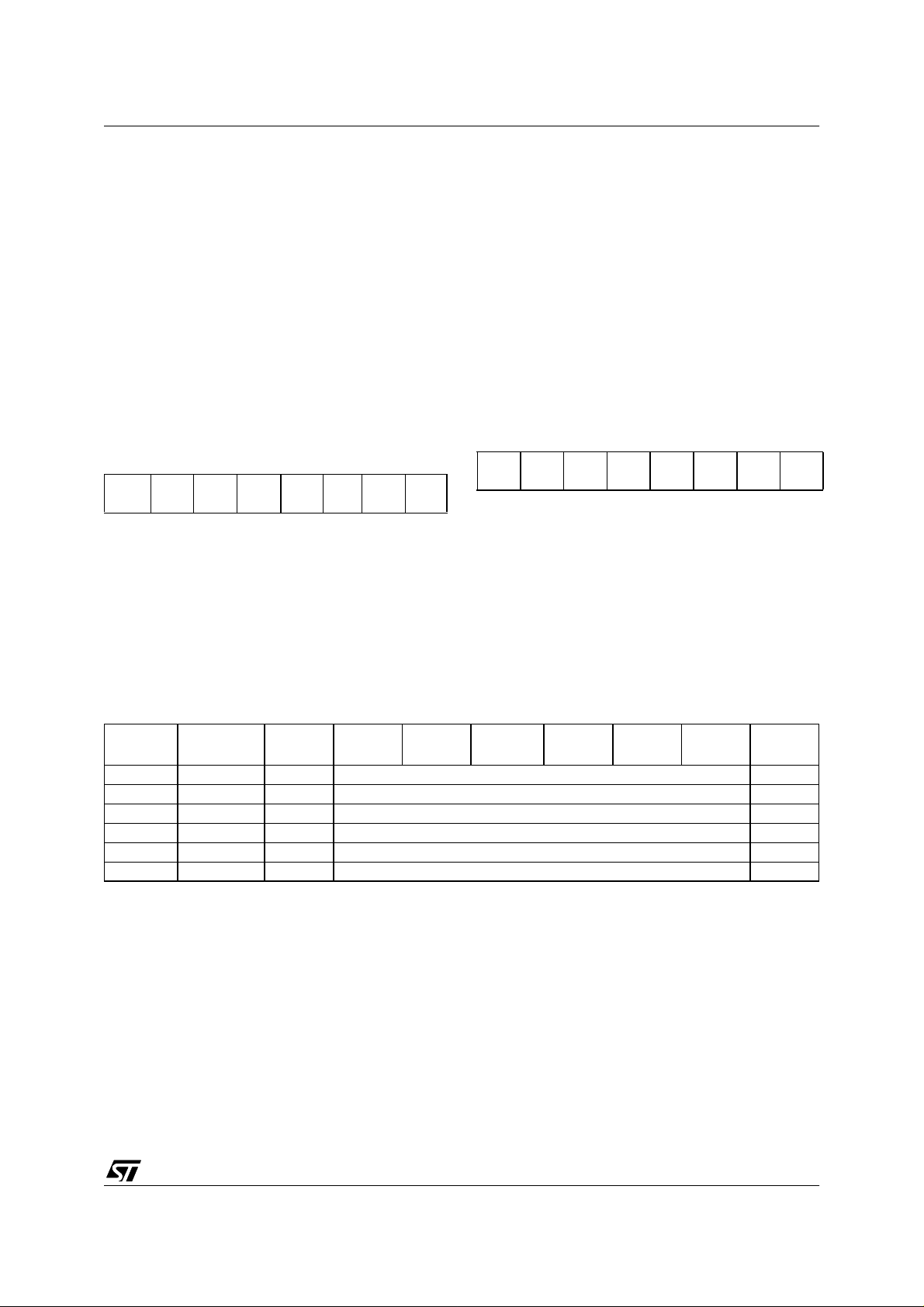
DATA REGISTERS (PxDR)
Port A Data Register (PADR): 0000h
Port B Data Register (PBDR): 0002h
Port C Data Register (PCDR): 0004h
Read/Write
Reset Value Port A: 0000 0000 (00h)
Reset Value Port B: 0000 0000 (00h)
Reset Value Port C: 1111 x000 (FXh)
Note: For Port C, unused bits (7-3) are not acces-
DATA DIRECTION REGISTER (PxDDR)
Port A Data Direction Register (PADDR): 0001h
Port B Data Direction Register (PBDDR): 0003h
Port C Data Direction Register (PCDDR): 0005h
Read/Write
Reset Value Port A: 0000 0000 (00h)
Reset Value Port B: 0000 0000 (00h)
Reset Value Port C: 1111 x000 (FXh)
Note: For Port C, unused bits (7-3) are not acces-
sible
sible.
70
70
D7 D6 D5 D4 D3 D2 D1 D0
DD7 DD6 DD 5 DD4 DD3 DD2 DD1 DD0
ST7263B
Data Direction Register 8 bits.
Bit 7:0 = D[7:0]
Data Register 8 bits.
The DR register has a specific behaviour according to the selected input/output configuration. Writing the DR register is always taken into account
even if the pin is configured as an input. Reading
Bit 7:0 = DD[7:0]
The DDR register gives the input /output direction
configuration of the pins. Each bit is set and
cleared by software.
0: Input mode
1: Output mode
the DR register returns ei ther the DR register latch
content (pin configured as output) or the digital value applied to the I/O pin (pin configured as input).
Table 13. I/O Ports Register Map
Address
(Hex.)
00 PADR MSB LSB
01 PADDR MSB LSB
02 PBDR MSB LSB
03 PBDDR MSB LSB
04 PCDR MSB LSB
05 PCDDR MSB LSB
Register
Label
7654 3210
31/132
Page 32

ST7263B
10 MISCELLANEOUS REGISTER
Address: 0009h — Read/Write
Reset Value: 0000 0000 (00h)
70
-----SMSUSBOEMCO
Bit 7:3 = Reserved
Bit 1 = USBOE
USB enable.
If this bit is set, the port PC2 outputs the USB output enable signal (at “1” when the ST7 USB is
transmitting data).
Unused bits 7-4 are set.
Bit 0 = MCO
Main Clock Out selection
This bit enables the MCO alternate function on the
Bit 2 = SMS
Slow Mode Select
.
This bit is set by software and only cleared by hardware after a reset. If this bit is set, it enables the use
of an internal divide-by-2 clock divider (refer to Fig-
ure 15 on page 19 ). The SMS bi t h as no ef fec t on
PA0 I/O port. It is set and cleared by software.
0: MCO alternate function disabled (I/O pin free for
general-purpose I/O)
1: MCO alternate function enabled (f
port)
the USB frequency.
0: Divide-by-2 disabled and CPU clock frequency
is standard
1: Divide-by-2 enabled and CPU clock frequency is
halved.
CPU
on I/O
32/132
Page 33
11 ON-CHIP PER IPHERALS
11.1 WATCHDOG TIMER (WDG)
ST7263B
11.1.1 Introduction
The Watchdog tim er is used to detect t he occurrence of a software fault, usually generated by external interference or by unforeseen logi cal conditions, which causes the application program to
abandon its normal seque nce. The W atchdog circuit generates an MCU reset o n expiry of a programmed time period, unless the program refresh-
es the counter’s contents before the T6 bit becomes cleared.
11.1.2 Main Features
■ Programmable ti mer (64 increments of 49,152
CPU cycles)
■ Programmable reset
■ Reset (if watchdog act iv ated) when the T6 bit
reaches zero
■ Optional reset on HALT instruction
(configurable by option byte)
■ Hardware Watchdog selectable by option byte.
11.1.3 Functional Description
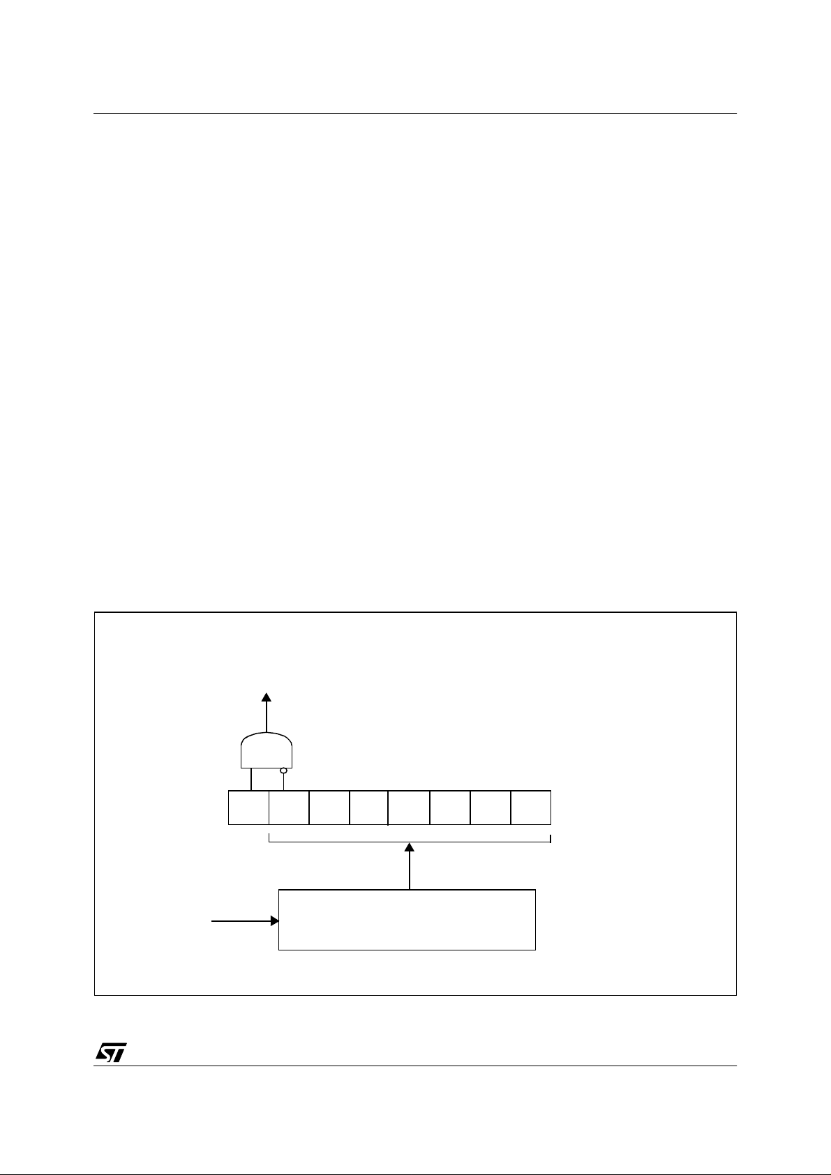
The counter value stored in the CR register (bits
T6:T0), is decremented every 49,152 machine cy-
Figure 23. Watchdog Block Diagram
cles, and the length of the timeout perio d can be
programmed by the user in 64 increments.
If the watchdog is activated (the WDGA bit is set)
and when the 7-bit timer (bits T6:T0) rolls over
from 40h to 3Fh (T6 becom es cleared), it initia tes
a reset cycle pulling low the reset pin for typically
500ns.
The application program must write in the CR register at regular intervals during normal operation to
prevent an MCU reset. The value to be stored in
the CR register must be between FFh and C0h
(see Table 14, ". Watchdog Timing (fCPU = 8
MHz)"):
– The WDGA bit is set (watchdog enabled)
– The T6 bit is set to prevent generating an imme-
diate reset
– The T5:T0 bits contain the number of increments
which represents the time delay before the
watchdog produces a reset.
f
CPU
RESET
WATCHDOG CONTROL REGISTER (CR)
WDGA
T6
T5
T4
T3
7-BIT DOWNCOU NTE R
CLOCK DIVIDER
49152
÷
T2
T1
T0
33/132
Page 34

ST7263B
WATCHD OG TI M E R (Cont’d)
Table 14. Watchdog Timing (f
CR Register
initial value
Max FFh 393.216
Min C0h 6.144
= 8 MHz)
CPU
WDG timeout period
(ms)
Notes: Following a reset, the watchdog is disa-
bled. Once activated it cannot be disabled, except
by a reset.
The T6 bit can be used to generat e a sof t ware reset (the WDGA bit is set and the T6 bit is cleared).
11.1.4 Software Watchdog Option
If Software Watchdog is selected by option byte,
the watchdog is disabled following a reset. Onc e
activated it cannot be disabled, except by a reset.
The T6 bit can be used to generat e a sof t ware reset (the WDGA bit is set and the T6 bit is cleared).
11.1.5 Hardware Watchdog Option
If Hardware Watchdog is selected by option b yte,
the watchdog is always active and the WDGA bit in
the CR is not used.
11.1.6 Low Power Modes
WAIT Instruction
No effect on Watchdog.
HALT Instruction
If the Watchdog reset on HALT option is selected
by option byte, a H ALT instruction causes an im mediate reset generation if th e Watchdog is activated (WDGA bit is set).
11.1.6.1 Using Halt Mode with the WDG (option)
If the Watchdog reset on HALT option is not selected by option byte, the Halt mo de can be used
when the watchdog is enabled.
In this case , th e HALT instr ucti on sto ps t he oscill ator. When the oscillator is stopped, the WDG stops
counting and is no longer able to generate a reset
until the microcontroller receives an external interrupt or a reset.
If an external interrupt is recei ve d, the WDG restarts counting after 4096 CPU clocks. If a reset is
generated, the WDG is disabled (reset state).
Recommendations
– Make sure that an external event is available to
wake up the microcontroller from Halt mode.
– Before executing the HALT instruction, refresh
the WDG counter, to avoid an unexpected WDG
reset immediately after waking up the microcontroller.
– When using an external interrupt to wake up the
microcontroller, reinitialize the corresponding I/O
as “Input Pull-up with Interrupt” before executing
the HALT instruction. The main reason for this is
that the I/O may be wrongly configured due to external interference or by an unforeseen logical
condition.
– For the same rea so n, r einitialize the level sen si -
tiveness of each external interrupt as a precautionary measure.
– The opcode for the HALT instruction is 0x8E. To
avoid an unexpected HALT instruction due to a
program counter failure, it is advised to clear all
occurrences of the data value 0x8E from memory. For example, avoid defining a constant in
ROM with the value 0x8E.
– As the HALT instruction clears the I bit in the CC
register to allow interrupts, the user may choose
to clear all pending interrupt bits before executing the HALT instruction. This avoids entering
other peripheral interrupt routines after executing
the external interrupt routine corresponding to
the wake-up event (reset or external interrupt).
11.1.7 Interrupts
None.
34/132
Page 35

WATCHD OG TI M E R (Cont’d)
11.1.8 Register Description
CONTROL REGISTER (CR)
Read/Write
hardware after a reset. When WDGA = 1, the
watchdog can generate a reset.
0: Watchdog disabled
1: Watchdog enabled
Reset Value: 0111 1111 (7Fh)
70
WDGA T6 T5 T4 T3 T2 T1 T0
Bit 6:0 = T[6:0]
These bits contain the decremented value. A reset
is produced when it rolls over from 40h to 3Fh (T6
becomes cleared).
7-bit timer (MSB to LSB).
ST7263B
Bit 7 = WDGA
Activation bit
.
This bit is set by software and only cleared by
Table 15. Watchdog Time r Register Map and Rese t Values
Address
(Hex.)
0Ch
Register
Label
WDGCR
Reset Value
7654 3210
WDGA
0
T6
1
T5
T4
1
1
T3
T2
1
1
T1
T0
1
1
35/132
Page 36

ST7263B
11.2 16-BIT TIMER
11.2.1 Introduction
The timer consists of a 16-bit free-running counter
driven by a programmable prescaler.
It may be used for a variety of purposes, including
pulse length measurement of up to two input signals (
input capture
put waveforms (
) or generation of up to two out-
output compare
and
PWM
).
Pulse lengths and waveform perio ds c an be m odulated from a few microseconds to several milliseconds using the timer prescaler and the CPU
clock prescaler.
Some ST7 devices have two on-chip 16-bit timers.
They are completely independent, and do not
share any resources. They are synchronized a fter
a MCU reset as long as the timer clock frequencies are not modified.
This description covers one or two 16-bit timers. In
ST7 devices with two timers, regi ster names are
prefixed with TA (Timer A) or TB (Timer B).
11.2.2 Main Features
■ Programmable prescaler: f
■ Overflow status flag and maskable interrupt
■ External clock inpu t (must be at least 4 times
slower than the CPU
clock speed) with the choice
divided by 2, 4 or 8.
CPU
of active edge
■ 1 or 2 Output Compare functions each with:
– 2 dedicated 16-bit registers
– 2 dedicated programmable signals
– 2 dedicated status flags
– 1 dedicated maskable interrupt
■ 1 or 2 Input Capture functions each with:
– 2 dedicated 16-bit registers
– 2 dedicated active edge selection signals
– 2 dedicated status flags
– 1 dedicated maskable interrupt
■ Pulse width modulation mode (PWM)
■ One pulse mode
■ Reduced Power Mode
■ 5 alternate functions on I/O ports (ICAP1, ICAP2,
OCMP1, OCMP2, EXTCLK)*
When reading an input signal on a non-bonded
pin, the value will always be ‘1’.
11.2.3 Functional Description
11.2.3.1 Counter
The main block of the Programmab le Timer is a
16-bit free running upcounter and its associated
16-bit registers. The 16-bit registers are made up
of two 8-bit registers called high & low.
Counter Register (CR):
– Counter High Register (CHR) is the most sig-
nific a nt by te ( MS Byte ).
– Counter Low Register (CLR) is the least sig-
nificant byte (LS Byte).
Alternate Counter Register (ACR)
– Alternate Count er Hi gh Regi ster ( ACHR) is th e
most significant byte (MS Byte).
– Alternate Counter Low Register (ACLR) is the
least significant byt e (LS Byte).
These two read-only 16-bit registers contain the
same value but with the difference that reading the
ACLR register does not clear the TOF bit (Timer
overflow flag), located in the Status register, (SR),
(see note at the end of paragraph titled 16-bit read
sequence).
Writing in the CLR register or ACLR register resets
the free running counter to the FFFCh value.
Both counters have a reset value of FFFCh (this is
the only value which is reloaded in the 16-bit timer). The reset value of both counters is also
FFFCh in One Pulse mode and PWM mode.
The timer clock depends on the cloc k control bits
of the CR2 register, as illustrated in Table 16,
"Clock C on t r ol B it s". The value in the c ounter reg-
ister repeats every 131072, 262144 or 524288
CPU clock cycles depending on the CC[1:0] bits.
The timer frequency c an be f
CPU
/2, f
CPU
/4, f
CPU
/8
or an external frequency.
The Block Diagram is shown in Figure 24.
*Note: Some timer pins may not available (not
bonded) in some ST7 devices. Refer to the device
pin out description.
36/132
Page 37
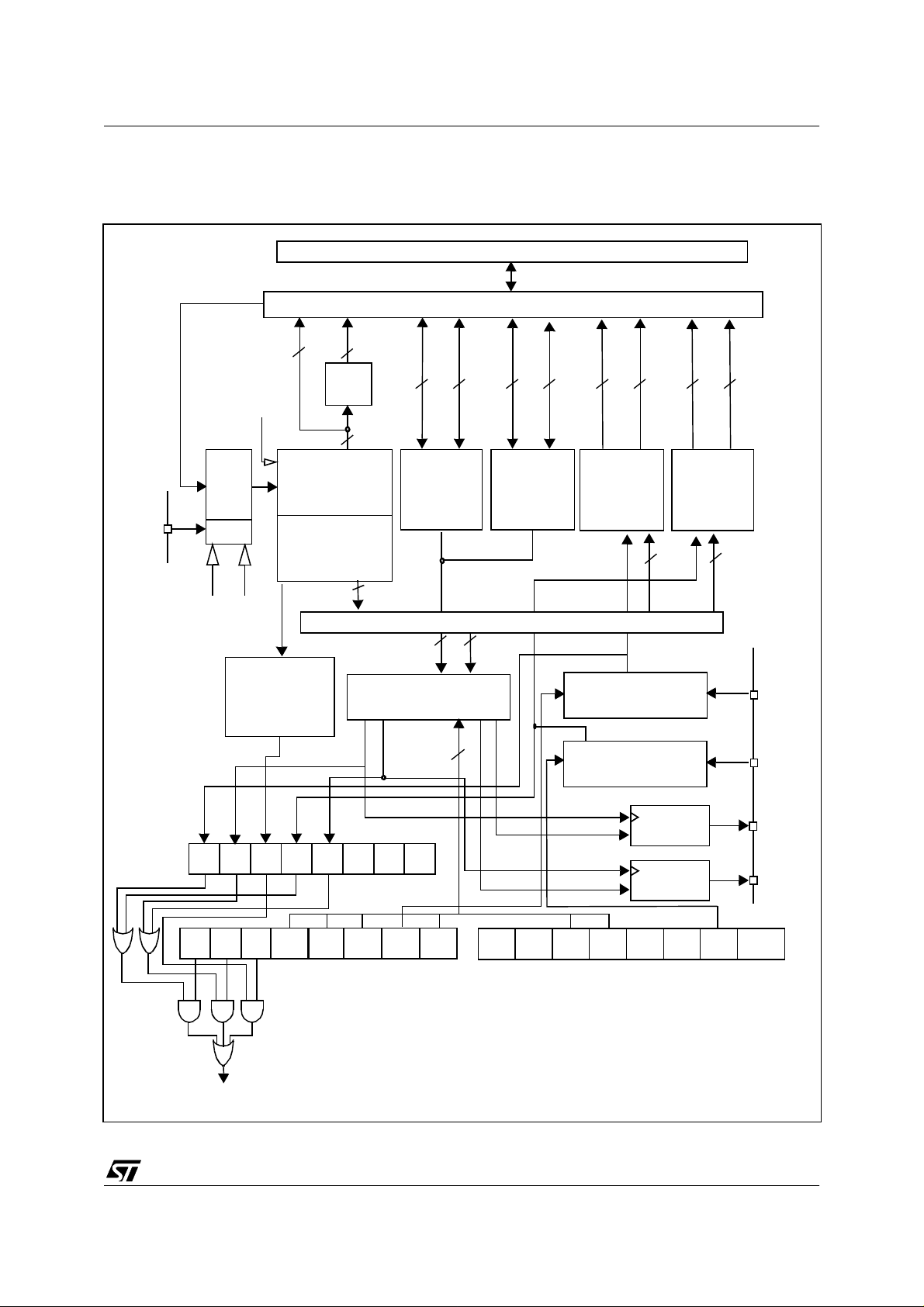
16-BIT TIMER (Cont’d)
Figure 24. Timer Block Diagram
f
CPU
ST7263B
ST7 INTERNAL BUS
MCU-PERIPHERAL INTERFACE
EXTCLK
pin
EXEDG
1/2
1/4
1/8
CC[1:0]
8 high
COUNTER
REGISTER
ALTERNATE
COUNTER
REGISTER
OVERFLOW
DETECT
CIRCUIT
8 low
8-bit
buffer
high
16
OUTPUT
COMPARE
REGISTER
16
TIMER INTERNAL BUS
OUTPUT COMPARE
CIRCUIT
low
1
16 16
6
8
low
high
OUTPUT
COMPARE
REGISTER
2
88 8
high
INPUT
CAPTURE
REGISTER
EDGE DETECT
CIRCUIT1
EDGE DETECT
CIRCUIT2
8
8 8 8
low
1
16
high
low
INPUT
CAPTURE
REGISTER
2
16
ICAP1
pin
ICAP2
pin
(See note)
TIMER INTERRUPT
ICF2ICF1
OCF2OCF1 TOF
TIMD
0
(Control/Status Register)
CSR
(Control Register 1) CR1
LATCH1
0
LATCH2
OC2E
PWMOC1E
OPMFOLV2ICIE OLVL1IEDG1OLVL2FOLV1OCIETOIE
IEDG2CC0CC1
(Control Register 2) CR2
Note: If IC, OC and TO interrupt requests ha ve separate vector s
then the last O R is not presen t (See device Interrupt Vector Tab l e)
OCMP1
pin
OCMP2
pin
EXEDG
37/132
Page 38
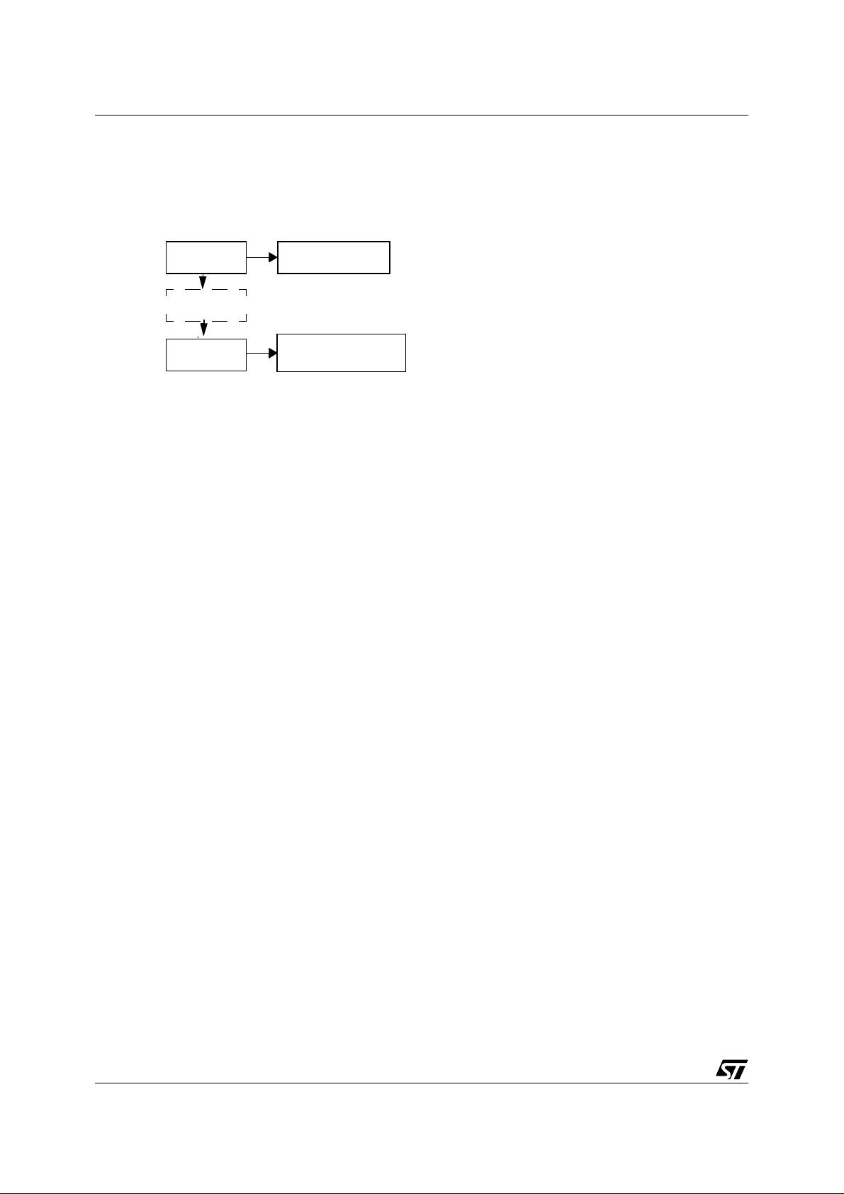
ST7263B
16-BIT TIMER (Cont’d)
16-bit read sequence: (from either the Counter
Register or the Alternate Counter Register).
Beginning of the sequence
Read
At t0
MS Byte
Other
instructions
Read
At t0 +∆t
LS Byte
Sequence completed
The user must read the MS Byte f irst, then the LS
Byte value is buffered automatically.
This buffered value rem ains unchanged until the
16-bit read sequence is completed, even if the
user reads the MS Byte several times.
After a complete reading sequence, if only the
CLR register or ACLR register are read, they return the LS Byte of the count value at the time of
the read.
Whatever the timer mode used (input capture, output compare, one pulse mode or P WM mode) an
overflow occurs when the counter rolls over from
FFFFh to 0000h then:
– The TOF bit of the SR register is set.
– A timer interrupt is generated if:
– TOIE bit of the CR1 register is set and
– I bit of the CC register is cleared.
If one of these cond itions is false, the interrupt remains pending to be issued as soon as they are
both true.
LS Byte
is buffered
Returns the buffered
LS Byte value at t0
Clearing the overflow interrupt request is done in
two steps:
1.Reading the SR register while the TOF bit is set.
2.An access (read or write) to the CLR register.
Notes: The TOF bit is not cleared by accesses to
ACLR register. The advantage of accessing the
ACLR register rather than the CLR register is that
it allows simultaneous use of the overflow function
and reading the free running counter at random
times (for example, to measure elapsed time) without the risk of clearing the TOF bit erroneously.
The timer is not affected by WAIT mode.
In HALT mode, the counter stops counting until the
mode is exited. Count ing then resumes from the
previous count (MCU awakened by an interrupt) or
from the reset count (MCU awakened by a Reset).
11.2.3.2 External Clock
The external clock (wh ere available) is selected if
CC0=1 and CC1=1 in the CR2 register.
The status of the EXEDG bit in the CR2 register
determines the type of level transition on the external clock pin EXTCLK that will trigger the free running counter.
The counter is synchronized with t he falling edge
of the internal CPU clock.
A minimum of four falling edges of the CPU clock
must occur between two consecutive active edges
of the external clock; thus the external clock frequency must be less than a quarter of the CPU
clock frequency.
38/132
Page 39
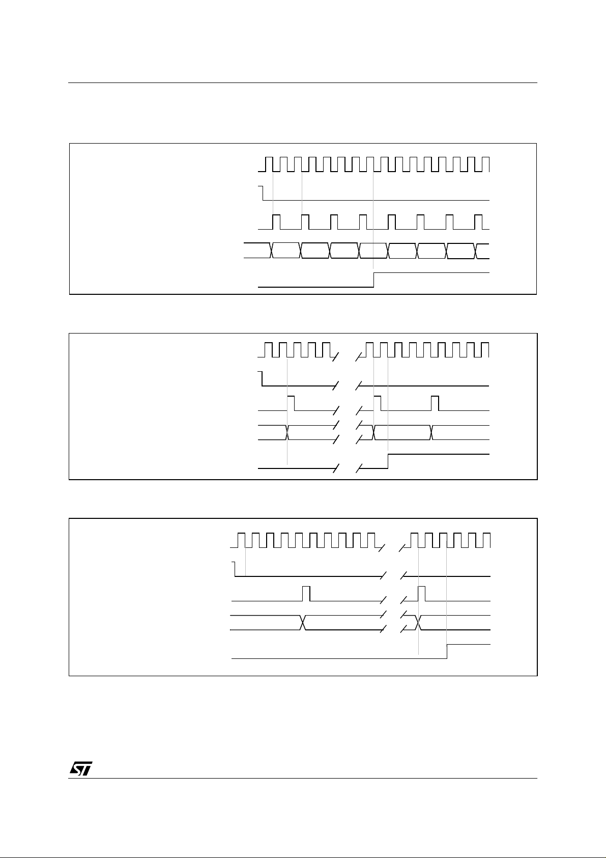
16-BIT TIMER (Cont’d)
Figure 25. Counter Timing Diagram, internal clock divided by 2
CPU CLOCK
INTERNAL RESET
TIMER CLOCK
ST7263B
COUNTER REGISTER
TIMER OVERFL OW FLAG (TOF)
FFFD FFFE FFFF 0000 0001 0002 0003
Figure 26. Counter Timing Diagram, internal clock divided by 4
CPU CLOCK
INTERNAL RESET
TIMER CLOCK
COUNTER REGI STER
TIMER OVERFLOW FLAG (TOF)
FFFC FFFD 0000 0001
Figure 27. Counter Timing Diagram, internal clock divided by 8
CPU CLOCK
INTERNAL RESET
TIMER CLOCK
COUNTER REGISTER
TIMER OVERFLOW FLAG (TOF)
FFFC FFFD
0000
Note: The MCU is in reset state when the internal reset signal is high, when it is low the MCU is running.
39/132
Page 40

ST7263B
16-BIT TIMER (Cont’d)
11.2.3.3 Input Capture
i
In this section, the index,
there are 2 input capture functions in the 16-bit
timer.
The two 16-bit input capture registers (IC1R and
IC2R) are used to latch the valu e of the free running counter after a transition is detected on the
ICAP
i
pin (see figure 5).
MS Byte LS Byte
ICiR IC
IC
i
R register is a read-only register.
The active transition is software programmable
i
through the IEDG
Timing resolution is one count of the free running
counter: (
Procedure:
To use the input capture function select the following in the CR2 register:
– Select the timer clock (CC[1:0]) (see Table 16,
"Clock Control Bits").
– Select the edge of the active transition on the
ICAP2 pin with the IEDG2 bit (the ICAP2 pin
must be configured as floating input or input with
pull-up without interrupt if this configuration is
available).
And select the following in the CR1 register:
– Set the ICI E bit to ge nerat e an in terrupt after an
input capture com ing from e ither the ICAP1 pin
or the ICAP2 pin
– Select the edge of the active transition on the
ICAP1 pin with the IEDG1 bit (the ICAP1pin must
be configured as floating inp ut or inp ut with pul l-
up without interrupt if this configuration is availa-
ble).
f
CPU
bit of Control Registers (CRi).
/CC[1:0]).
, may be 1 or 2 because
i
HR ICiLR
When an input capture occurs:
– ICF
i
bit is set.
– The IC
running counter on the active transition on the
ICAP
– A timer interrupt is generated if the ICIE bit i s s e t
and the I bit is cleared in the CC register. Otherwise, the interrupt remains pending until both
conditions become true.
Clearing the Input Capture in terrupt request (i.e.
clearing the ICF
1. Reading the SR register while the ICF
2. An acces s (read or write) to the IC
Notes:
1. After reading the IC
2. The IC
3. The 2 input capture functions can be used
4. In O ne pulse Mode and PWM mode only I nput
5. The alternate inputs (ICAP1 & ICAP2) are
6. The TOF bit can be used with interrupt genera-
i
R register contains t he val ue of the free
i
pin (see Figure 29).
i
bit) is done in two steps:
i
bit is set.
iLR
register.
i
HR register, transfer of
input capture data is inhibited and ICF
i
never be set until the IC
read.
i
R register contains the free running
counter value which corresponds to the most
recent input capture.
together even if the timer also uses the 2 output
compare functions.
Capture 2 can be used.
always directly connecte d to the timer. So any
transitions on these pins activates the input
capture function.
Moreover if one of the ICAP
as an input and the s econd one as an output,
an interrupt can be generated if the user toggles the output pin and if the ICIE bit is set.
This can be avoided if the in put capture func-
i
is disabled by reading the ICiHR (see note
tion
1).
tion in order to m easure events t hat go b eyond
the timer range (FFFFh).
LR register is also
i
pins is configured
i
will
40/132
Page 41
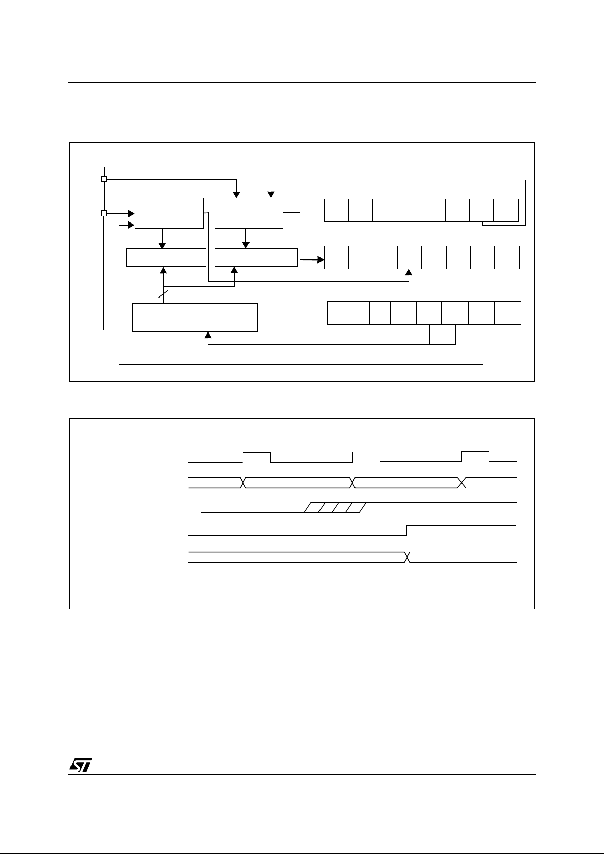
16-BIT TIMER (Cont’d)
Figure 28. Input Capture Block Diagram
ST7263B
ICAP1
pin
ICAP2
pin
EDGE DETECT
CIRCUIT2
IC2R Register
16-BIT
16-BIT FREE RUNNING
COUNTER
EDGE DETECT
CIRCUIT1
IC1R Register
Figure 29. Input Capture Timing Diagram
TIMER CLOCK
ICIE
(Control Register 1) CR1
IEDG1
(Status Register) SR
ICF2ICF1 000
(Control Register 2) CR2
IEDG2
CC0
CC1
COUNTER REGISTER
ICAPi PIN
ICAPi FLAG
ICAPi REGISTER
Note: The rising edge is the ac tive edge.
FF01 FF02 FF03
FF03
41/132
Page 42

ST7263B
16-BIT TIMER (Cont’d)
11.2.3.4 Output Compare
i
In this section, the index,
there are 2 output compare functions in the 16-bit
timer .
This function can be used to control an output
waveform or indicate when a period of time has
elapsed.
When a match is found bet ween the Output Compare register and the free running counter, the output compare function:
– Assigns pins with a programmable value if the
OC
i
E bit is set
– Sets a flag in the status register
– Generates an interrupt if enabled
Two 16-bit registers Output Compare Register 1
(OC1R) and Output Compare Register 2 (OC2R)
contain the value to be com pared to the counter
register each timer clock cycle.
MS Byte LS Byte
i
ROC
OC
These registers are readable and writable and are
not affected by the timer hardware. A reset event
changes the OC
i
R value to 8000h.
Timing resolution is one count of the free running
counter: (
f
CPU/
CC[1:0]
Procedure:
To use the output compare function, select the following in the CR2 register:
– Set the OC
OCMP
i
E bit if an output is needed then the
i
pin is dedicated to the output com pare
signal.
– Select the timer clock (CC[1:0]) (see Table 16,
"Clock Control Bits").
And select the following in the CR1 register:
– Select the OLVL
i
bit to applied to the OCMPi pins
after the match occurs.
– Set the OC IE bit to generate an interrupt if it is
needed.
When a match is found between OCRi register
and CR register:
i
– OCF
bit is set.
, may be 1 or 2 because
i
HR OCiLR
).
i
– The OCMP
pin takes OLVLi bit value (OCMPi
pin latch is forced low during reset).
– A timer interrupt is generated if the OCIE bit is
set in the CR1 register and the I bit is cleared in
the CC register (CC).
i
The OC
R register value required for a specific timing application can be c alcul ated using the following f ormula:
∆t * f
∆ OC
i
R =
CPU
PRESC
Where:
∆t = Output compare period (in seconds)
f
= CPU clock frequency (in hertz)
CPU
PRESC
= Timer prescaler factor (2, 4 or 8 de-
pending on CC[1:0] bits, see Ta ble 16,
"Clock Control Bits")
If the timer clock is an external clock, the formula
is:
∆ OC
i
R = ∆t
* fEXT
Where:
∆t = Output compare period (in seconds)
f
= External timer clock frequency (in hertz)
EXT
Clearing the output compare interrupt request (i.e.
i
clearing the OCF
1. Reading the SR register while the OCF
i
set.
2. An access (read or write) to the OC
The following procedure is recommended to pre-
vent the OCF
it is read and the write to the OC
– Write to the OC
are inhibited).
– Read the SR register (first step of the clearance
of the OCF
– Write to the OC
compare function and clears the OCF
bit) is done by:
i
i
bit from being set between the time
i
R register:
i
HR register (further compares
i
bit, which may be already set).
i
LR register (enables the output
i
bit is
LR register.
i
bit).
42/132
Page 43
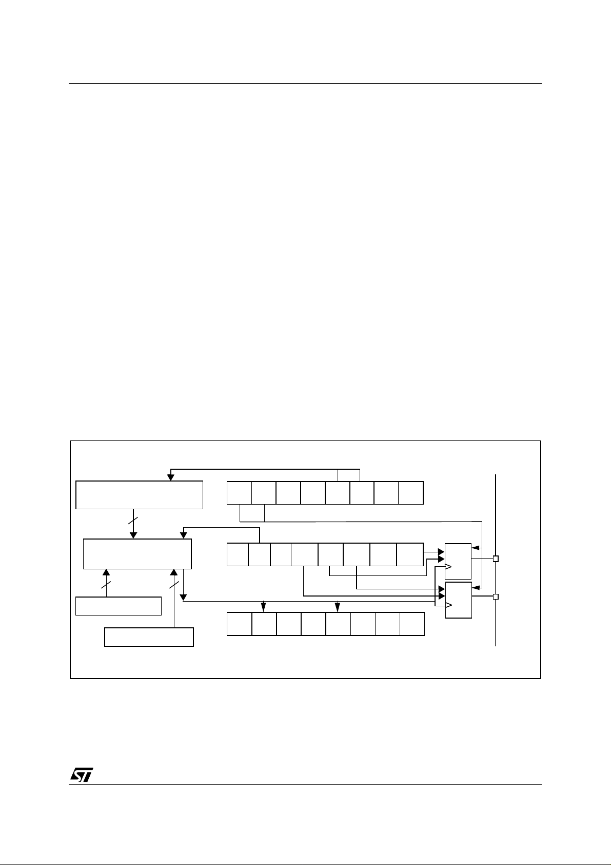
16-BIT TIMER (Cont’d)
Notes:
1. After a processor write cycle to the OC
iHR
reg-
ister, the output compare function is inhibited
iLR
until the OC
2. If the OC
general I/O port and the OLVL
register is also written.
i
E bit is not set, the OCMPi pin is a
i
bit will not
appear when a match is f ound but an interrupt
could be generated if the OCIE bit is set.
3. When the timer clock is f
OCMP
i
are set while the counter value equals
i
the OC
R register value (see Figure 31 on page
/2, OCFi and
CPU
44). This behaviour is the same in OPM or
PWM mode.
When the timer clock is f
external clock mode, O CF
/4, f
CPU
i
and OCMPi are set
while the counter value equals the OC
CPU
/8 or in
i
R regis-
ter value plus 1 (see Figure 32 on page 44).
4. The output compare functions can be used both
for generating external events on the OCMP
pins even if the input capture mode is also
used.
i
5. The value in the 16-bit OC
OLV
i
bit should be changed after each suc-
R register and the
cessful comparison in order to control an output
waveform or establish a new elapsed timeout.
Forced Compare Output capabili ty
i
When the FOLV
bit is set by software, the OLVL
bit is copied to the OCMPi pin. The OLVi bit has to
be toggled in ord er to t oggle th e OCMP
it is enabled (OC
i
E bit=1). The OCFi bit is then not
set by hardware, and thus no interrupt request is
generated.
i
The FOLVL
bits have no effect in both one pulse
mode and PWM mode.
i
ST7263B
i
pin when
i
Figure 30. Output Compare Block Diagram
16 BIT FREE RUNNING
COUNTER
16-bit
OUTPUT COMPARE
CIRCUIT
16-bit
OC1R Register
16-bit
OC2R Register
OC1E CC0CC1
OC2E
(Control Register 2) CR2
(Control Register 1) CR1
FOLV2 FOLV1
(Status Register) SR
OLVL1OLVL2OCIE
000OCF2OCF1
Latch
1
Latch
2
OCMP1
Pin
OCMP2
Pin
43/132
Page 44
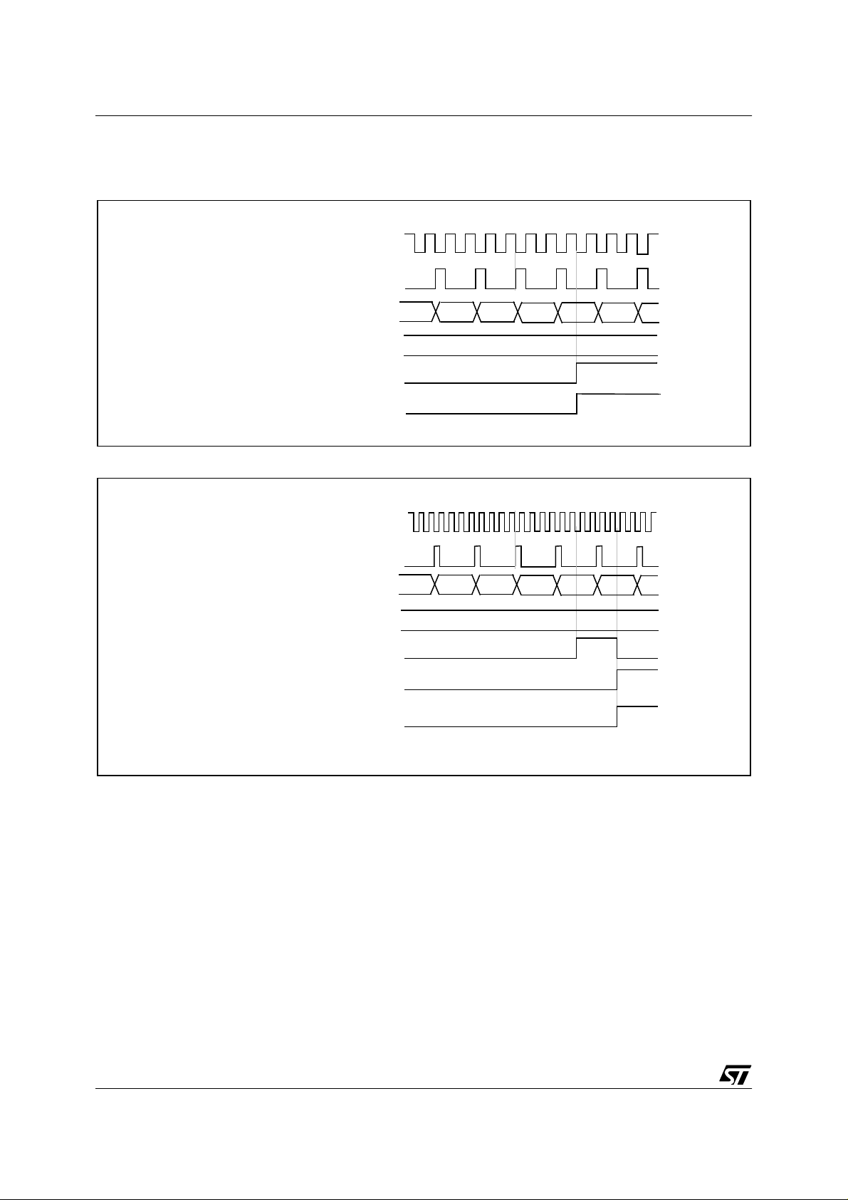
ST7263B
16-BIT TIMER (Cont’d)
Figure 31. Output Compare Timing Diagram, f
INTERNAL CPU CLOC K
TIMER CLOCK
TIMER
=f
CPU
/2
COUNTER REGISTER
OUTPUT COMPARE REGISTER
OUTPUT COMPARE FLAG
i
OCMP
i
(OCRi)
i
(OCFi)
PIN (OLVLi=1)
Figure 32. Output Compare Timing Diagram, f
INTERNAL CPU CLOC K
TIMER CLOCK
COUNTER REGISTER
OUTPUT COMPARE REGISTER
COMPARE REGISTER
OUTPUT COMPARE FLAG
OCMPi PIN (OLVLi=1)
i
(OCRi)
i
LATCH
i
(OCFi)
2ED0 2ED1 2ED2
=f
TIMER
CPU
2ED0 2ED 1 2ED 2
/4
2ED3
2ED3
2ED3
2ED3
2ED42ECF
2ED42ECF
44/132
Page 45
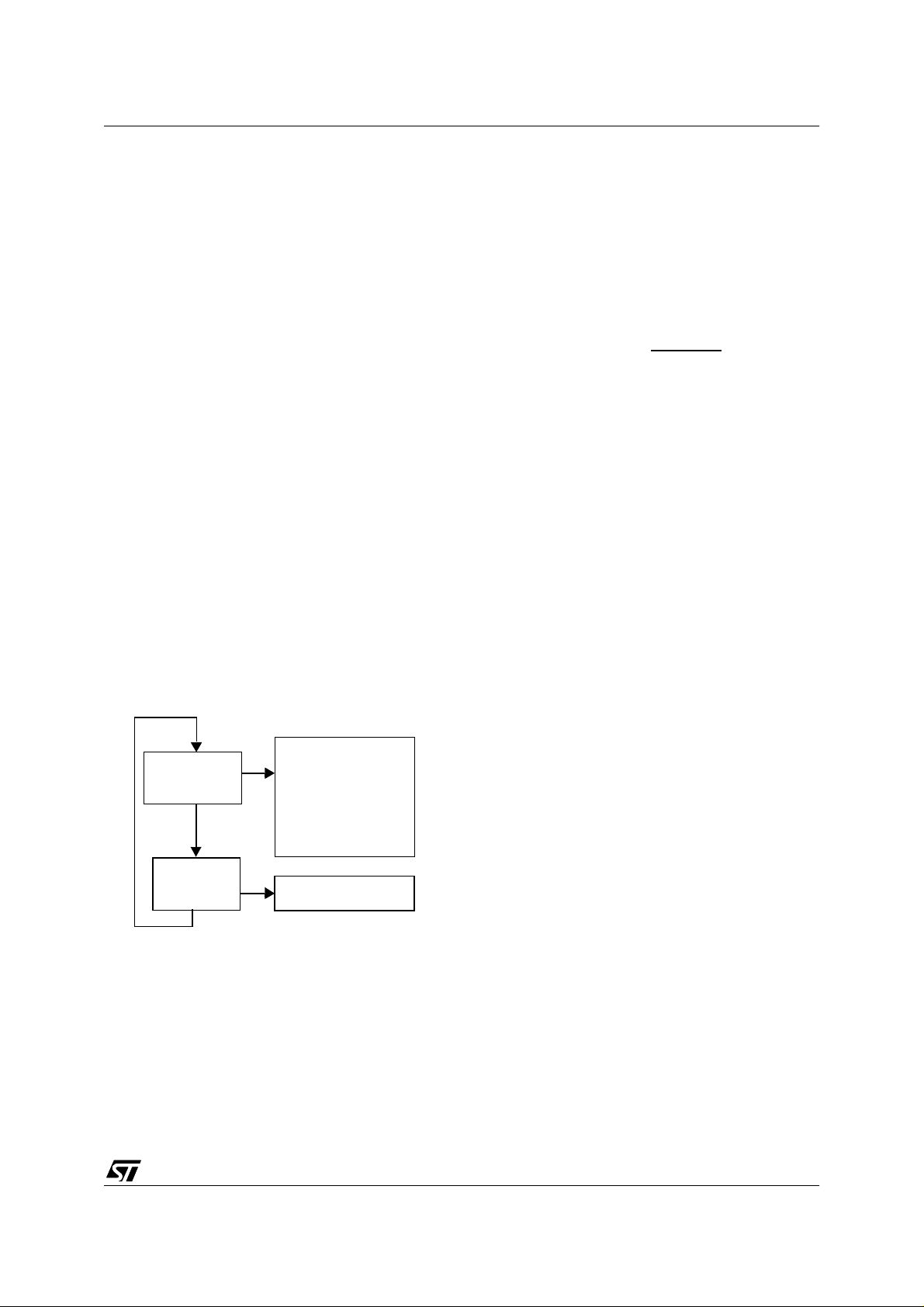
16-BIT TIMER (Cont’d)
11.2.3.5 One Pulse Mode
One Pulse mode enables the generation of a
pulse when an external event occurs. This mode is
selected via the OPM bit in the CR2 register.
The one pulse mode uses the Input Capture1
function and the Output Compare1 function.
Procedure:
To use one pulse mode:
1. Load the OC1R register with the value corresponding to the length of the pulse (see the formula in the op po s ite column).
2. Select the following in the CR1 register:
– Using the OLVL1 bit, select the level to be ap-
plied to the OCMP1 pin after the pulse.
– Using the OLVL2 bit, select the level to be ap-
plied to the OCMP1 pin during the pulse.
– Select the edge of the a ctive trans ition o n th e
ICAP1 pin with the IEDG1 bit
(the ICAP1 pin
must be configured as floating input).
3. Select the following in the CR2 register:
– Set the OC1E bit, the OCMP1 pin is then ded-
icated to the Output Compare 1 function.
– Set the OPM bit.
– Select the timer clock CC[1:0] (see T able 16,
"Clock Control Bits" ).
ST7263B
Clearing the Input Capture in terrupt request (i.e.
clearing the ICF
1. Reading the SR register while the ICF
2. An acces s (read or write) to the IC
The OC1R register value required for a specific
timing application can be calculated usi ng the following formula:
OC
Where:
t = Pulse period (in seconds)
= CPU clock frequency (in hertz)
f
CPU
PRESC
= Timer prescaler factor (2, 4 or 8 depend-
If the timer clock is an external clock the formula is:
Wher e:
t = Pulse period (in seconds)
f
= External timer clock frequency (in hertz)
EXT
When the value of the counter is equal to the value
of the contents of t he OC1R register, the OLV L1
bit is output on the OCMP1 pin, (See Figure 33).
i
bit) is done in two steps:
i
bit is set.
iLR
register.
t
f
*
i
R Value =
CPU
PRESC
- 5
ing on the CC[1:0] bits, see Table 16,
"Clock Control Bits")
OCiR = t
* fEXT
-5
One pulse mode cycle
When
event occurs
on ICAP1
ICR1 = Counter
OCMP1 = OLVL2
Counter is reset
to FFFCh
ICF1 bit is set
When
Counter
= OC1R
OCMP1 = OLVL1
Then, on a valid event on the ICAP1 pin, the counter is initialized to FFFCh and OLVL2 bit is loaded
on the OCMP1 pin, the ICF1 bit is set and the value FFFDh is loaded in the IC1R register.
Because the ICF1 bit is set when an active edge
occurs, an interrupt can be generated if the ICIE
bit is set.
Notes:
1. The OCF1 bit cannot be set by hardware in one
pulse mode but the OCF2 bit can gen erate an
Output Compare interrupt.
2. W hen the Pulse Width Modulation (PWM) and
One Pulse Mode (OPM) bits are both set, the
PWM mode is the only active one.
3. If OLVL1=OLVL2 a continuous signal will be
seen on the OCMP1 pin.
4. The ICAP1 pin can not be used to perform input
capture. The ICAP2 pin can be used t o perfo rm
input capture (ICF2 can be set and IC2R can be
loaded) but the user must take care that the
counter is reset each time a valid edge o ccurs
on the ICAP1 pin and ICF1 can also generates
interrupt if ICIE is set.
5. W hen one pulse mode is used OC1R is dedicated to this mode. Nevertheless OC2R and
OCF2 can be used to indicate a period of time
has been elapsed but canno t generate an output waveform because the level OLVL2 is dedicated to the one pulse mode.
45/132
Page 46
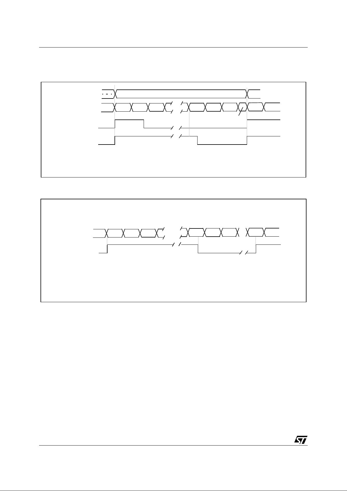
ST7263B
16-BIT TIMER (Cont’d)
Figure 33. One Pulse Mode Timing Example
IC1R
COUNTER
ICAP1
OCMP1
01F8
FFFC FFFD FFFE 2ED0 2ED1 2ED2
01F8
OLVL2
2ED3
2ED3
FFFC FFFD
OLVL2OLVL1
compare1
Note: IEDG1=1, OC1R=2ED 0h, OLV L1=0, OLVL2=1
Figure 34. P ul se Wi dt h M odulation Mode Timin g E xa m p le wi t h 2 Out p ut C om pare Functi ons
COUNTER
OCMP1
FFFC FFFD FFFE
34E2
2ED0 2ED1 2ED2
OLVL2
34E2 FFFC
OLVL2OLVL1
compare2 compare1 compare2
Note: OC1R=2ED0h, OC2R=34E2, OLVL1=0, OLVL2= 1
Note: On timers with only 1 Output Compare register, a fixed frequency PWM signal can be generated us-
ing the output compare and the counter overflow to define the pulse length.
46/132
Page 47
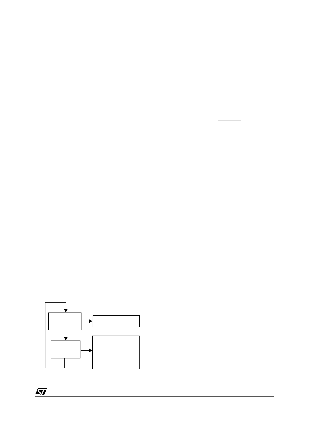
16-BIT TIMER (Cont’d)
11.2.3.6 Pulse Width Modulation Mode
Pulse Width Modulation (PWM) mode enables the
generation of a signal wi th a frequency a nd pul se
length determined by the value of the OC1R and
OC2R registers.
Pulse Width Modulation mode uses the complete
Output Compare 1 fu nction plus the OC2R register, and so this functionality can not be used when
PWM mode is activated.
In PWM mode, double buffering is implemented on
the output compare registers. Any new values written in the OC1R and OC2R registers are taken
into account only a t the end of the PWM perio d
(OC2) to avoid spikes on the PWM output pin
(OCMP1).
Procedure
To use pulse width modulation mode:
1. Load the OC2R register with the value corresponding to the period of the signal using th e
formula in the opposite column.
2. Load the OC1R register with the value corresponding to the period of the pulse if (OLVL1=0
and OLVL2=1) using th e formula in the opposite column.
3. Select the following in the CR1 register:
– Using the OLVL1 bit, select the level to be ap-
plied to the OCMP1 pin after a successful
comparison with the OC1R register.
– Using the OLVL2 bit, select the level to be ap-
plied to the OCMP1 pin after a successful
comparison with the OC2R register.
4. Select the following in the CR2 register:
– Set OC1E bit: the OCMP1 pin is then dedicat-
ed to the output compare 1 function.
– Set the PWM bit.
– Select the timer clock (CC[1:0]) (see Table 16,
"Clock Control Bits" ).
Pulse Width Modulation cycle
When
Counter
OCMP1 = OLVL1
= OC1R
When
Counter
= OC2R
OCMP1 = OLVL2
Counter is reset
to FFFCh
ST7263B
If OLVL1=1 and OLVL2=0 the lengt h of the positive pulse is the difference between the OC2R and
OC1R registers.
If OLVL1=OLV L2 a c ont inuo us signal will be seen
on the OCMP1 pin.
The OC
ing application can be c alcul ated using the following f ormula:
Where:
t = Signal or pulse period (in seconds)
f
CPU
PRESC
If the timer clock is an external clock the formula is:
Wher e:
t = Signal or pulse period (in seconds)
f
EXT
The Output Compare 2 event causes the counter
to be initialized to FFFCh (See Figure 34)
Notes:
1. After a write instruction to the OCiHR register,
2. The OCF1 and OCF2 bits cannot be set by
3. The ICF1 bit is set by hardware when the coun-
4. In PW M mode the ICA P1 pin can not be used
5. W hen the Pulse Width Modulation (PWM) and
i
R register value required for a specific tim-
t
f
*
i
R Value =
OC
CPU
PRESC
- 5
= CPU clock frequency (in hertz)
= Timer prescaler factor (2, 4 or 8 depend-
ing on CC[1:0] bits, see Table 16,
"Clock Control Bits")
OCiR = t
* fEXT
-5
= External timer clock frequency (in hertz)
the output compare function is inhibited until the
i
LR register is also written.
OC
hardware in PWM mode therefore the Output
Compare interrupt is inhibited.
ter reaches the OC2R value and can produce a
timer interrupt if the ICIE bit is set and the I bit is
cleared.
to perform input capture because it is disconnected to the timer. The ICAP2 pin can be used
to perform input capture (ICF2 can be set and
IC2R can be loaded) but the user must take
care that the counter is reset each period and
ICF1 can also generates interrupt if ICIE is set.
One Pulse Mode (OPM) bits are both set, the
PWM mode is the only active one.
ICF1 bit is set
47/132
Page 48
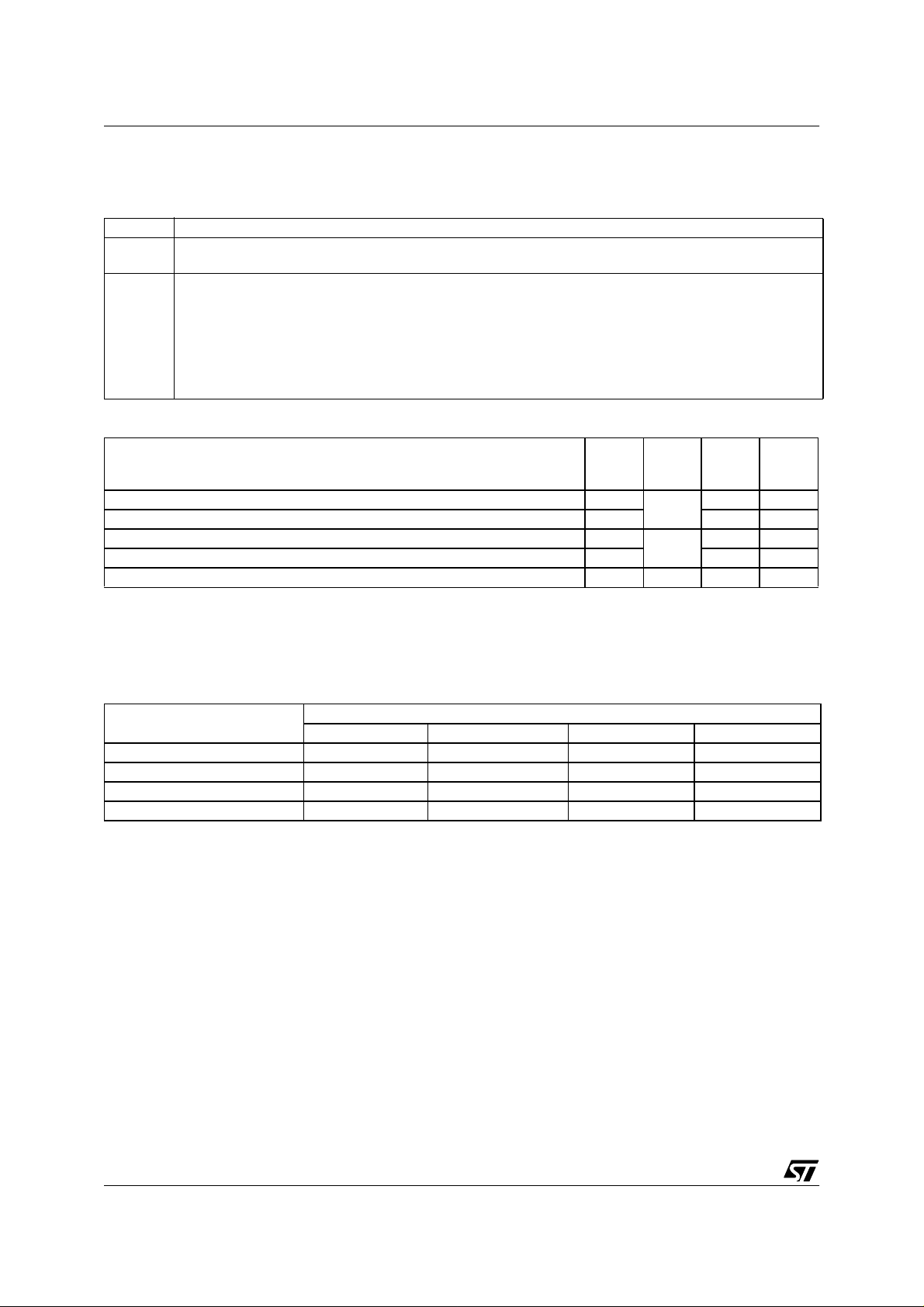
ST7263B
16-BIT TIMER (Cont’d)
11.2.4 Low Power Modes
Mode Description
WAIT
HALT
11.2.5 Interrupts
Input Capture 1 event/Counter reset in PWM mode ICF1
Input Capture 2 event ICF2 Yes No
Output Compare 1 event (not available in PWM mode) OCF1
Output Compare 2 event (not available in PWM mode) OCF2 Yes No
Timer Overflow event TOF TOIE Yes No
No effect on 16-bit Timer.
Timer interrupts cause the device to exit from WAIT mode.
16-bit Timer registers are frozen.
In HALT mode, the counter stops counting until Halt mode is exited. Counting resumes from the previous
count when the MCU is woken up by an interrupt with “exit from HALT mode” capability or from the counter
reset value when the MCU is woken up by a RESET.
If an input capture event occurs on the ICAP
ly, when the MCU is woken up by an interrupt with “exit from HALT mode” capability, the ICF
the counter value present when exiting from HALT mode is captured into the IC
Interrupt Event
i
pin, the input capture detection circuitry is armed. Consequent-
i
bit is set, and
i
R register.
Event
Flag
Enable
Control
Bit
ICIE
OCIE
Exit
from
Wait
Yes No
Yes No
Exit
from
Halt
Note: The 16-bit Timer interrupt ev ents are co nnecte d to the same inte rrupt vector (see In terrupts chap-
ter). These events generate an interrupt if the correspo nding Enable Control Bit is set and the interrupt
mask in the CC register i s reset (RIM instructio n).
11.2.6 Summary of Timer modes
MODES
Input Capture (1 and/or 2) Yes Yes Yes Yes
Output Compare (1 and/or 2) Yes Yes Yes Yes
One Pulse Mode No Not Recommended
PWM Mode No Not Recommended
Input Capture 1 Input Capture 2 Output Compare 1 Output Compare 2
TIMER RESOURCES
1)
3)
No Partially
No No
2)
1) See note 4 in Section 11.2.3.5, "One Pulse Mode"
2) See note 5 in Section 11.2.3.5, "One Pulse Mode"
3) See note 4 in Sect ion 11.2.3.6, "Pulse Wid th Modulation Mode"
48/132
Page 49

16-BIT TIMER (Cont’d)
11.2.7 Register Description
Each Timer is associated with three control and
status registers, and with six pairs of data registers
(16-bit values) relating to the two input captures,
the two output compares, the count er and the a lternate counter.
ST7263B
Bit 4 = FOLV2
This bit is set and cleared by software.
0: No effect on the OCMP2 pin.
1:Forces the OLVL2 bit to be copied to the
OCMP2 pin, if the OC 2E bit is set and even if
there is no successful compariso n.
Forced Output Compare 2.
CONTROL REGISTER 1 (CR1)
Read/Write
Reset Value: 0000 0000 (00h)
70
ICIE OCIE TOIE FOLV2 FOLV1 OLVL2 IEDG1 OLVL1
Bit 3 = FOLV1
This bit is set and cleared by software.
0: No effect on the OCMP1 pin.
1: Forces OLVL1 to be copied to the OCMP1 pin, if
the OC1E bit is set and e ven if there i s no successful compari son.
Bit 2 = OLVL2
Bit 7 = ICIE
Input Capture Interrupt Enable.
0: Interrupt is inhibited.
1: A timer interrupt is generated whenever the
ICF1 or ICF2 bit of the SR register is set.
Bit 6 = OCIE
Output Compare Interrupt Enable.
0: Interrupt is inhibited.
1: A timer interrupt is generated whenever the
OCF1 or OCF2 bit of the SR register is set.
This bit is copied to the OCMP2 pin whenev er a
successful compa rison occurs with the OC2R register and OCxE is set in the CR2 register. This value is copied to the OCMP1 pin in One Pulse Mode
and Pulse Width Modulation mode.
Bit 1 = IEDG1
This bit determines wh ich type of level transition
on the ICAP1 pin will trigger the capture.
0: A falling edge triggers the capture.
Forced Output Compare 1.
Output Level 2.
Input Edge 1.
1: A rising edge triggers the capture.
Bit 5 = TOIE
0: Interrupt is inhibited.
1: A timer interrupt is enabled whenever the TOF
bit of the SR register is set.
Timer Overflow Interrupt Enable.
Bit 0 = OLVL1
Output Level 1.
The OLVL1 bi t is c opied to t he OCMP1 pin whenever a successful comparison occurs with the
OC1R register and the OC 1E bit is s et in the CR2
register.
49/132
Page 50
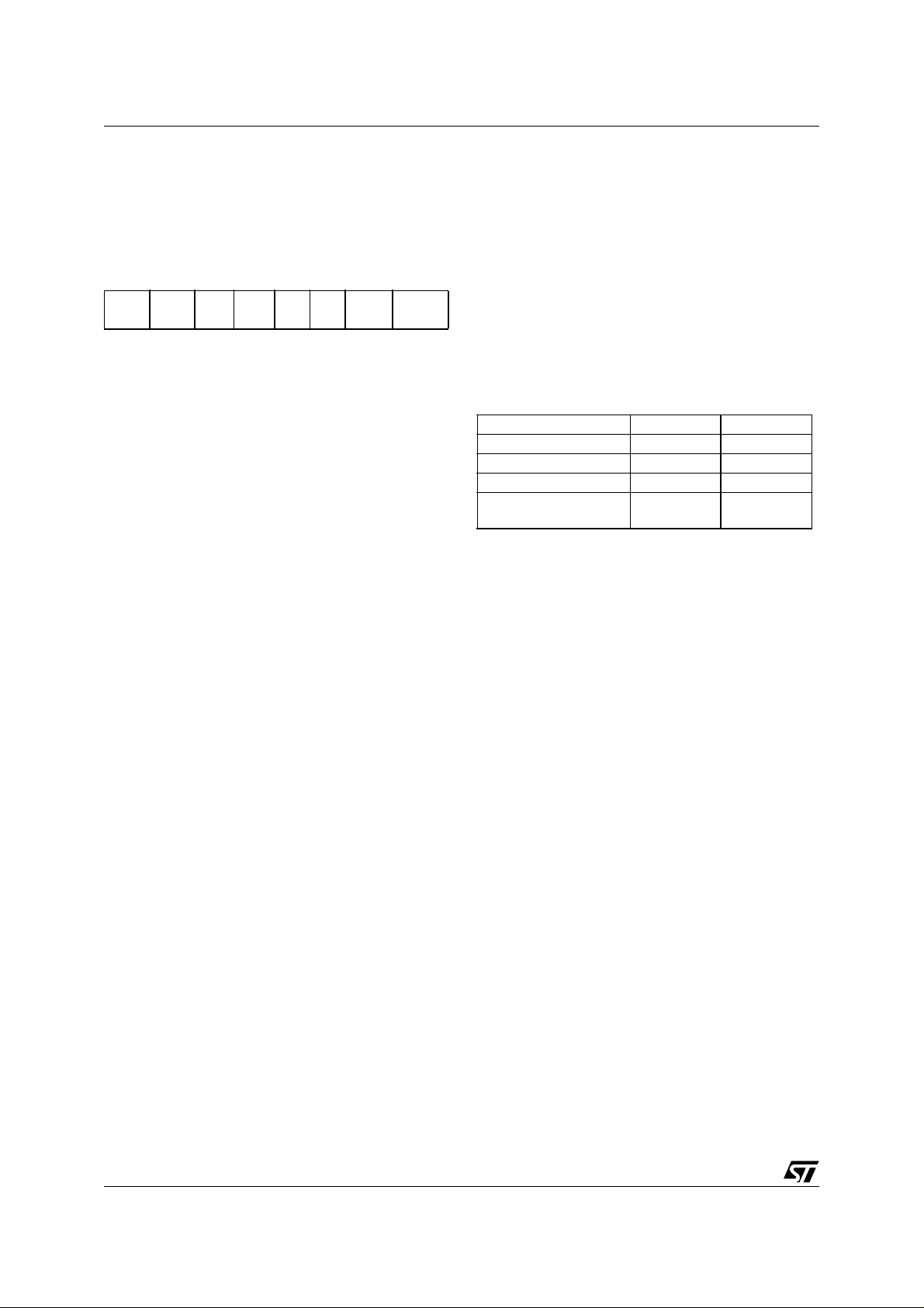
ST7263B
16-BIT TIMER (Cont’d)
CONTROL REGISTER 2 (CR2)
Read/Write
Reset Value: 0000 0000 (00h)
70
OC1E O C2E OPM PWM CC1 CC0 IEDG2 EXEDG
Bit 4 = PWM
0: PWM mode is not active.
1: PWM mode is active, the OCMP 1 pin outputs a
programmable cyclic signal; the length of the
pulse depends on the value of OC1R register;
the period depends on the value of OC2R register.
Pulse Width Modulation.
Bit 7 = OC1E
Output Compare 1 Pin Enable.
This bit is used only to outp ut the signal from the
timer on the OCMP1 pin (OLV1 in Output Compare mode, both OLV1 and OLV2 in PWM and
one-pulse mode). Whatever the value of the OC1E
bit, the Output Compare 1 function of the timer remains active.
0: OCMP1 pin alternate f unction disa bled (I/O pin
free for general-purpose I/O).
1: OCMP1 pin alternate function enabled.
Bit 6 = OC2E
Output Compare 2 Pin Enable.
This bit is used only to outp ut the signal from the
timer on the OCMP2 pin (OLV2 in Output Compare mode). Whatever the value of the OC2E bit,
the Output Compare 2 function of the timer remains active.
0: OCMP2 pin alternate f unction disa bled (I/O pin
free for general-purpose I/O).
1: OCMP2 pin alternate function enabled.
Bit 5 = OPM
One Pulse Mode.
0: One Pulse Mode is not active.
1: One Pulse Mode is active, the ICAP1 pin can be
used to trigger one pulse on the OCMP1 pin; the
active transition is g iven by the I EDG1 bit. Th e
length of the generated pulse depends on the
contents of the OC1R register.
Bit 3, 2 = CC[1:0]
Clock Control.
The timer clock mode depends on these bits:
Table 16. Clock Control Bits
Timer Clock CC1 CC0
f
/ 4 0 0
CPU
f
/ 2 0 1
CPU
f
/ 8 1 0
CPU
External Clock (where
available)
11
Note: If the external clock pin is not available, programming the external clock configuration stops
the counter.
Bit 1 = IEDG 2
Input Edge 2.
This bit determines wh ich type of level transition
on the ICAP2 pin will trigger the capture.
0: A falling edge triggers the capture.
1: A rising edge triggers the capture.
Bit 0 = EXEDG
External Clock Edge.
This bit determines wh ich type of level transition
on the external clock pin EXTCLK wi ll trigger the
counter register.
0: A falling edge triggers the counter register.
1: A rising edge triggers the counter register.
50/132
Page 51

16-BIT TIMER (Cont’d)
CONTROL/STATUS REGISTER (CSR)
Read Only (except bit 2 R/W)
Note: Reading or writing the ACLR register does
not clear TOF.
Reset Value: xxxx x0xx (xxh)
70
ICF1 OCF 1 TOF ICF2 OCF2 TIMD 0 0
Bit 4 = ICF2
0: No input capture (reset value).
1: An input capture has occurred on the ICAP2
Input Capture Flag 2.
pin. To clear this bit, first read the SR register,
then read or write the low byte of the IC2R
Bit 7 = ICF1
Input Capture Flag 1.
(IC2LR) register.
0: No input capture (reset value).
1: An input capture has occurred on the ICAP1 pin
or the counter has reached th e OC2R value in
PWM mode. To clear this bit, first read the SR
register, then read or write the lo w byte of the
IC1R (IC1LR) register.
Bit 3 = OCF2
Output Compare Flag 2.
0: No match (reset value).
1: The content of the free running counter has
matched the cont ent of the OC2R register. T o
clear this bit, first read the SR register, then read
or write the low byte of the OC2R (OC2LR) regBit 6 = OCF1
Output Compare Flag 1.
ister.
0: No match (reset value).
1: The content of the free running counter has
matched the content of the OC1R register. To
clear this bit, first read the SR register, t hen read
or write the low byte of the OC1R (OC1LR) register.
Bit 2 = TIMD
This bit is set and cleared by software. When set, it
freezes the timer prescaler an d counter and disabled the output functions (OCMP1 and OCMP2
pins) to reduce power consumption. Access to the
Timer disable.
timer registers is still available, allowing the timer
Bit 5 = TOF
Timer Overflow Flag.
0: No timer overflow (reset value).
1:The free running counter rolled over from FFFFh
to 0000h. To clear this bit, first read the SR reg-
configuration to be changed, or the count er reset,
while it is disabled.
0: Timer enabled
1: Timer prescaler, counter and outputs disabled
ister, then read or write the low byte of the CR
(CLR) register.
Bits 1:0 = Reserved, must be kept cleared.
ST7263B
51/132
Page 52
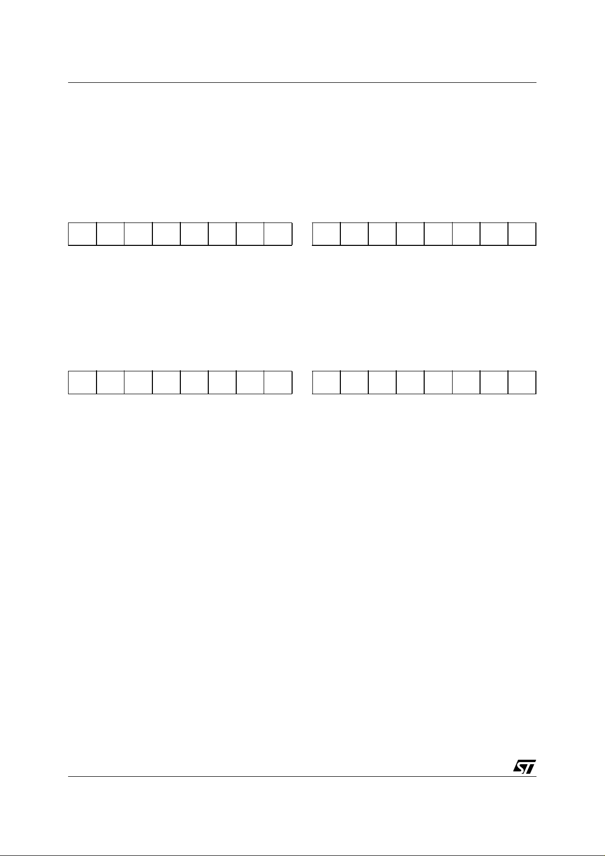
ST7263B
16-BIT TIMER (Cont’d)
INPUT CAPTURE 1 HIGH REGISTER (IC1HR)
Read Only
Reset Value: Undefined
This is an 8-bit read only register that contains the
high part of the counter value (transferred by the
input capture 1 event).
OUTPUT COMPARE 1 HIGH REGISTER
(OC1HR)
Read/Write
Reset Value: 1000 0000 (80h)
This is an 8-bit re gister tha t co ntains t he hi gh part
of the value to be compared to the CHR register.
70
MSB LSB
INPUT CAPTURE 1 LOW REGISTER (IC1LR)
Read Only
Reset Value: Undefined
This is an 8-bit read only register that contains the
low part of the counter value (transferred by the input capture 1 event).
70
MSB LSB
70
MSB LSB
OUTPUT COMPARE 1 LOW REGISTER
(OC1LR)
Read/Write
Reset Value: 0000 0000 (00h)
This is an 8-bit register that contains the low part of
the value to be compared to the CLR register.
70
MSB LSB
52/132
Page 53
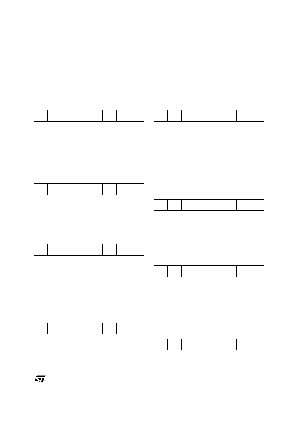
16-BIT TIMER (Cont’d)
OUTPUT COMPARE 2 HIGH REGISTER
(OC2HR)
Read/Write
Reset Value: 1000 0000 (80h)
This is an 8-bit register that cont ains the high part
of the value to be compared to th e CHR register.
ST7263B
ALTERNATE COUNTER HIGH REGISTER
(ACHR)
Read Only
Reset Value: 1111 1111 (FFh)
This is an 8-bit re gister tha t co ntains t he hi gh part
of the counter value.
70
MSB LSB
OUTPUT COMPARE 2 LOW REGISTER
(OC2LR)
Read/Write
Reset Value: 0000 0000 (00h)
This is an 8-bit register that contains the low part of
the value to be compared to the CLR register.
70
70
MSB LSB
ALTERNATE COUNTER LOW REGISTER
(ACLR)
Read Only
Reset Value: 1111 1100 (FCh)
This is an 8-bit register that contains the low part of
the counter value. A write to this register resets the
counter. An access to this register after an access
to CSR register does no t clear the TOF bit i n the
CSR register.
MSB LSB
COUNTER HIGH REGISTER (CHR)
70
MSB LSB
Read Only
Reset Value: 1111 1111 (FFh)
This is an 8-bit register that cont ains the high part
of the counter value.
70
INPUT CAPTURE 2 HIGH REGISTER (IC2HR)
Read Only
Reset Value: Undefined
This is an 8-bit read only register that contains the
high part of the counter value (transferred by the
MSB LSB
Input Capture 2 event).
70
COUNTER LOW REGISTER (CLR)
MSB LSB
Read Only
Reset Value: 1111 1100 (FCh)
This is an 8-bit register that contains the low part of
the counter value. A write to this register resets the
counter. An access to this register after accessing
the CSR register clears the TOF bit.
70
INPUT CAPTURE 2 LOW REGISTER (IC2LR)
Read Only
Reset Value: Undefined
This is an 8-bit read only register that contains the
low part of the counter value (transferred by the In-
put Capture 2 event).
MSB LSB
70
MSB LSB
53/132
Page 54

ST7263B
16-BIT TIMER (Cont’d)
Table 17. 16-Bit Timer Register Map and Reset Values
Address
(Hex.)
11
12
13
14
15
16
17
18
19
1A
1B
1C
1D
1E
1F
Register
Label
CR2
Reset Value
CR1
Reset Value
SR
Reset Value
IC1HR
Reset Value
IC1LR
Reset Value
OC1HR
Reset Value
OC1LR
Reset Value
CHR
Reset Value
CLR
Reset Value
ACHR
Reset Value
ACLR
Reset Value
IC2HR
Reset Value
IC2LR
Reset Value
OC2HR
Reset Value
OC2LR
Reset Value
76543210
OC1E0OC2E
0
ICIE
0
ICF1
0
MSB LSB
MSB LSB
MSB
1
MSB
0
MSB
1
MSB
1
MSB
1
MSB
1
MSB LSB
MSB LSB
MSB
1
MSB
0
OCIE
0
OCF1
0
0
0
1
1
1
1
0
0
OPM
0
TOIE0FOLV20FOLV10OLVL20IEDG10OLVL1
TOF
0
-
0
-
0
-
1
-
1
-
1
-
1
-
0
-
0
PWM
0
ICF2
0
0
0
1
1
1
1
0
0
CC1
0
OCF2
0
-
0
-
0
-
1
-
1
-
1
-
1
-
0
-
0
CC0
0
TIMD
0
-
0
-
0
-
1
-
1
-
1
-
1
-
0
-
0
IEDG20EXEDG
0
0
0
0
-
0
-
0
-
1
-
0
-
1
-
0
-
0
-
0
0
0
LSB
0
LSB
0
LSB
1
LSB
0
LSB
1
LSB
0
LSB
0
LSB
0
54/132
Page 55

11.3 SERIAL COMMUNICATIONS INTERFACE (SCI)
ST7263B
11.3.1 Introduction
The Serial Communications Interface (SCI) offers
a flexible means of full-duplex data exchange with
external equipment requiring an indust ry stand ard
NRZ asynchronous serial data format.
11.3.2 Main Features
■ Full duplex, asynchronous communi catio ns
■ NRZ standard format (Mark/Space)
■ Independently programmable transmit and
receive baud rates up to 250K baud.
■ Programmable data word length (8 or 9 bits)
■ Receive buffer full, Transmit buffer empty and
End of Transmission flags
■ Two receiver wake-up modes:
– Address bit (MSB)
– Idle line
■ Muting function for multiprocessor configurations
■ Separate enable bits for Transmitter and
Receiver
■ Four error detection flags:
– Overrun error
– Noise error
– Frame error
– Parity error
■ Five interrupt sources with flags:
– Transmit data register empty
– Transmission complete
– Receive data register full
– Idle line received
– Overrun error detected
■ Parity control:
– Transmits parity bit
– Checks parity of received data byte
■ Reduced power consumption mode
11.3.3 General Description
The interface is externally connected to another
device by two pins (see Figure 36):
– TDO: Transmit Data Output. When the transmit-
ter and the receiver are disabled, the output pin
returns to its I/O port configuration. When the
transmitter is enabled and nothing is to be transmitted, the TDO pin is at high level.
– RDI: Receive Data Input is the serial data input.
Oversampling techniques are used for data recovery by discriminating between valid incoming
data and noise.
Through these pins, serial data is transmitted and
received as frames comprising:
– An Idle Line prior to transmission or reception
– A start bit
– A data word (8 or 9 bits) least significant bit first
– A Stop bit indicating that the frame is complete.
55/132
Page 56
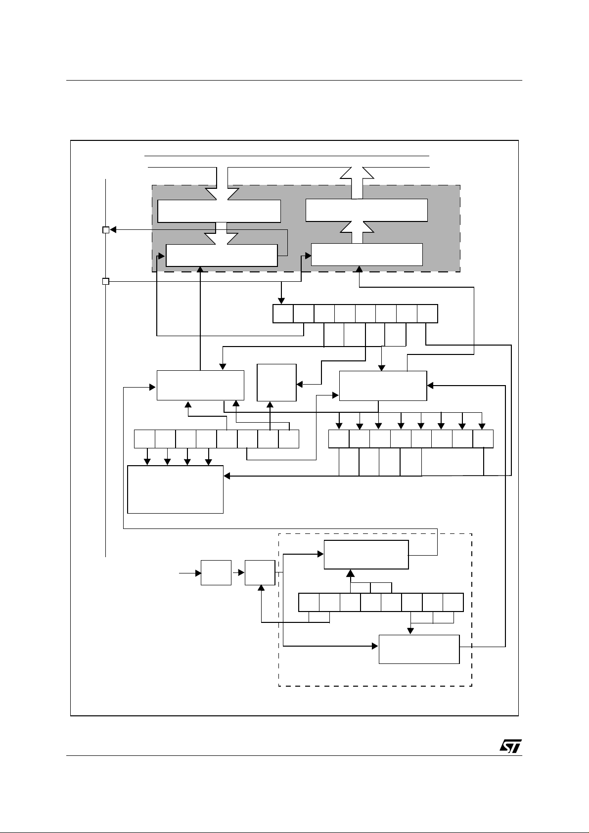
ST7263B
SERIAL COMMUNICATIONS INTERFACE (Cont’d)
Figure 35. SCI Block Diagram
TDO
RDI
Write
Transmit Data Register (TDR)
Transmit Shift Register
TRANSMIT
CONTROL
CR2
Read
(DATA REGISTER) DR
Received Data Register (RDR)
Received Shift Register
R8 T8 SCID M WAKE PCE PS PIE
WAKE
UP
UNIT
SBKRWURETEILIERIETCIETIE
RECEIVER
CONTROL
TDRE TC RDRF IDLE OR NF FE PE
CR1
RECEIVER
CLOCK
SR
56/132
SCI
INTERRUPT
CONTROL
TRANSMITTER
CLOCK
f
CPU
/16
/PR
TRANSMITTER RATE
CONTROL
SCP1
BAUD RATE GENERATOR
SCP0
SCT2
SCT1SCT0SCR2SCR1SCR0
BRR
RECEIVER RAT E
CONTRO L
Page 57
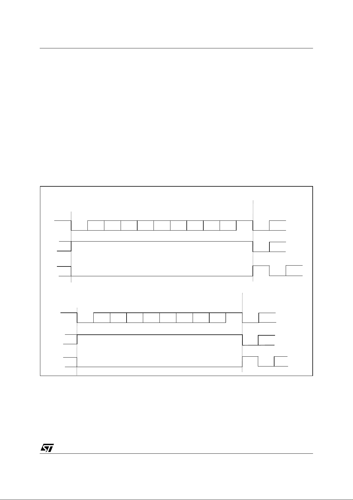
SERIAL COMMUNICATIONS INTERFACE (Cont’d)
11.3.4 Functional Description
The block diagram of the S erial Control Interface,
is shown in Figure 35. It contains 6 dedicated reg-
isters:
– Two co ntrol registers (SCICR1 & SCICR2)
– A status register (SCISR)
– A baud rate register (SCIBRR)
Refer to the register descriptions in Section
11.3.7for the definitions of each bit.
11.3.4.1 Serial Data Format
Word length may be selected as being either 8 or 9
bits by programming the M bi t in the SCICR1 register (see Figure 35).
Figure 36. Word Length Programming
ST7263B
The TDO pin is in low state during the start bit.
The TDO pin is in high state during the stop bit.
An Idle character is interpreted as an entire frame
of “1”s followed by t he start bit of the n ext frame
which contains data.
A Break character is interpreted on receiving “0”s
for some multiple of the frame period. At the end of
the last break frame the transm itter inserts an extra “1” bit to acknowledge the start bit.
9-bit Word length (M bit is set)
Data Frame
Start
Bit
Bit0 Bit1
Bit2
Bit3 Bit4
Idle Frame
Break Frame
8-bit Word length (M bit is reset)
Data Frame
Start
Bit
Bit0 Bit1
Bit2
Bit3 Bit4 Bit5
Idle Frame
Break Frame
Bit5 Bit6
Bit6
Possible
Parity
Bit7
Possible
Parity
Bit
Bit7
Bit
Bit8
Stop
Bit
Next Data Frame
Next
Start
Stop
Bit
Bit
Start
Bit
Extra
’1’
Next Data Frame
Next
Start
Bit
Start
Bit
Start
Extra
’1’
Bit
Start
Bit
57/132
Page 58

ST7263B
SERIAL COMMUNICATIONS INTERFACE (Cont’d)
11.3.4.2 Transmitter
The transmitter can send data words of either 8 or
9 bits depending on the M bit status. W hen the M
bit is set, word length is 9 bits and the 9th bit (the
MSB) has to be stored in the T8 bit in the SCICR 1
register.
Character Transmission
During an SCI transmission, data shifts out least
significant bit first on t he TDO pin. In this m ode,
the SCIDR register consists of a buffer (TDR) between the internal bus and the transmit shift register (see Figure 35).
Procedure
– Sele ct the M bit to define the word length.
– Sele ct the desired baud rate using the SCIBRR
register.
– Set the TE bit to assign the TDO pin to the alter-
nate function and to send a idle frame as first
transmission.
– Access the SCISR register and write the data to
send in the SCIDR register (this sequence clears
the TDRE bit). Repeat this sequence for each
data to be transmitted.
Clearing the TDRE bit is a lways perf ormed by the
following software sequence:
1. An access to the SCISR register
2. A write to the SCIDR register
The TDRE bit is set by hardware and it indicates:
– The TDR register is empty.
– The dat a transfer is beginning.
– The next data can be written in the SCIDR r egis-
ter without overwriting the previous data.
This flag generates an interrupt if the TIE bit is set
and the I bit is cleared in the CCR register.
When a transmission is taking place, a write instruction to the SCIDR regi ster stores the data i n
the TDR register and which is copied in the shift
register at the end of the current transmission.
When no transmission is ta king place, a write instruction to the SCIDR register places the data directly in the shift register, the data transmission
starts, and the TDRE bit is immediately set.
When a frame trans mission is com plete (after the
stop bit or after the break frame) the TC bit is set
and an interrupt is generated if the TCIE is set and
the I bit is cleared in the CCR register.
Clearing the TC bit is pe rformed by the following
software sequence:
1. An access to the SCISR register
2. A write to the SCIDR register
Note: The TDRE and TC bits are cleared by the
same software sequence.
Break Characters
Setting the SBK bit loads the shift register with a
break character. The break frame length depends
on the M bit (see Figure 36).
As long as the SBK bit is set, the SCI send break
frames to the T DO pin. After clearing this bit by
software the SCI insert a logic 1 bit at th e end of
the last break frame to guarantee the recognition
of the start bit of the next frame.
Idle Characters
Setting the TE bit drives the SCI t o send an idle
frame before the first data frame.
Clearing and then setting the TE bit during a transmission sends an idle frame after the current word.
Note: Resetting and setting t he TE bit causes t he
data in the TDR register to be lost . Therefore the
best time to toggle the TE bit is when the TDRE bit
is set i.e. before writing the next byte in the SCIDR.
58/132
Page 59

SERIAL COMMUNICATIONS INTERFACE (Cont’d)
11.3.4.3 Receiver
The SCI can receive data words of either 8 or 9
bits. When the M bit i s set, word length is 9 bits
and the MSB is stored in the R8 bit in the SCICR1
register.
Character Reception
During a SCI reception, data shifts in least significant bit first through the RDI pin. In this mode, the
SCIDR register consists or a buffer (RDR) between the internal bus and the received shift register (see Figure 35).
Procedure
– Sele ct the M bit to define the word length.
– Sele ct the desired baud rate using the SCIBRR
register.
– Set the RE bit, this enables the receiver which
begins searching for a start bit.
When a character is received:
– The RDRF bit is set. It indicates that the content
of the shift register is transferred to the RDR.
– An interrupt is generated if the RIE bit is set and
the I bit is cl eared in the CCR register.
– The error flags can be set if a frame error, noise
or an overrun error has been detected during re-
ception.
Clearing the RDRF bit is performed by the following
software sequence done by:
1. An access to the SCISR register
2. A read to the SCIDR register.
The RDRF bit must be cleared before the end of t he
reception of the next character to avoid an overrun
error.
Break Character
When a break character is received, the SPI handles it as a framing error.
Idle Character
When a idle frame is detected, there is the same
procedure as a data received character plus an interrupt if the ILIE bit is set and the I bit is cleared in
the CCR register.
ST7263B
Overrun Error
An overrun error occurs when a character is received when RDRF has not been reset. Data can
not be transferred from the shift register to the
RDR register as long as the RDRF bit is not
cleared.
When a overrun error occurs:
– The OR bit is set.
– The RDR content will not be lost.
– The shift register will be overwritten.
– An interrupt is generated if the RIE bit is set and
the I bit is cleared in the CCR register.
The OR bit is reset by an access to the SCISR register followed by a SCIDR register read operation.
Noise Error
Oversampling techniques are used for data recovery by discriminating between v alid inc oming dat a
and noise.
When noise is detected in a frame:
– The NF is set at the rising edge of the RDRF bit.
– Data is transferred from the Shift register to the
SCIDR register.
– No interrupt is generated. However this bit rises
at the same time as the RDRF bit which itself
generates an interrupt.
The NF bit is reset by a SCISR register read operation followed by a SCIDR register read operation.
Framing E rror
A framing error is detected when:
– The stop bit is not recognized on reception at the
expected time, following either a de-synchroni-
zation or excessive noise.
– A break is received.
When the framing error is detected:
– the FE bit is set by hardware
– Data is transferred from the Shift register to the
SCIDR register.
– No interrupt is generated. However this bit rises
at the same time as the RDRF bit which itself
generates an interrupt.
The FE bit is reset by a SCISR register read oper-
ation followed by a SCIDR register read operation.
59/132
Page 60

ST7263B
SERIAL COMMUNICATIONS INTERFACE (Cont’d)
11.3.4.4 Baud Rate Generation
The baud rate for the receiver a nd trans mitter (Rx
and Tx) are set independent ly and calculated as
follo ws:
(16
f
CPU
PR)*RR
*
Tx =
(16
CPU
PR)*TR
*
Rx =
f
with:
PR = 1, 3, 4 or 13 (see SCP[1:0] bits)
TR = 1, 2, 4, 8, 16, 32, 64,128
(see SCT[2:0] bits)
RR = 1, 2, 4, 8, 16, 32, 64,128
(see SCR[2:0] bits)
All these bits are in the SCIBRR register.
Example: If f
is 8 MHz (normal mode) and if
CPU
PR=13 and TR=RR=1, the transmit and receive
baud rates are 38400 baud.
Note: The baud rate registers MUST NOT be
changed while the transmitter or the receiver is enabled.
11.3.4.5 Receiver Muting and Wake-up Feature
In multiprocessor configurations it is often desirable that only the intended message recipient
should actively receive the full message contents,
thus reducing redundant SCI service overhead for
all non addressed receivers.
The non addressed devices may be placed in
sleep mode by means of the muting function.
Setting the RWU b it by software puts the SCI in
Sleep mode:
All the reception status bits can not be set.
All the receive interrupts are inhibited.
A muted receiver may be awakened by one of the
following two ways:
– by Idle Line detection if the WAKE bit is reset,
– by Address Mark detection if the WAKE bit is set.
Receiver wakes-up by Idle Line detection when
the Receive line has recognised an Idle Frame.
Then the RWU bit is reset by hardware but the
IDLE bit is not set.
Receiver wakes-up by Address Mark detection
when it received a “1” as the most significant bit of
a word, thus indicating that the message is an address. The reception of this particular word wakes
up the receiver, resets the RW U bit and sets the
RDRF bit, which allows the receiver to receiv e thi s
word normally and to use it as an address word.
Caution: In Mute mode, do not write to the
SCICR2 register. If the SCI is in Mute mode during
the read operation (RWU=1) and a address mark
wake up event o ccurs (RWU is reset) before t he
write operation, the RW U bit will be set again by
this write operation. Consequently the address
byte is lost and the SCI is not woken up from Mute
mode.
60/132
Page 61
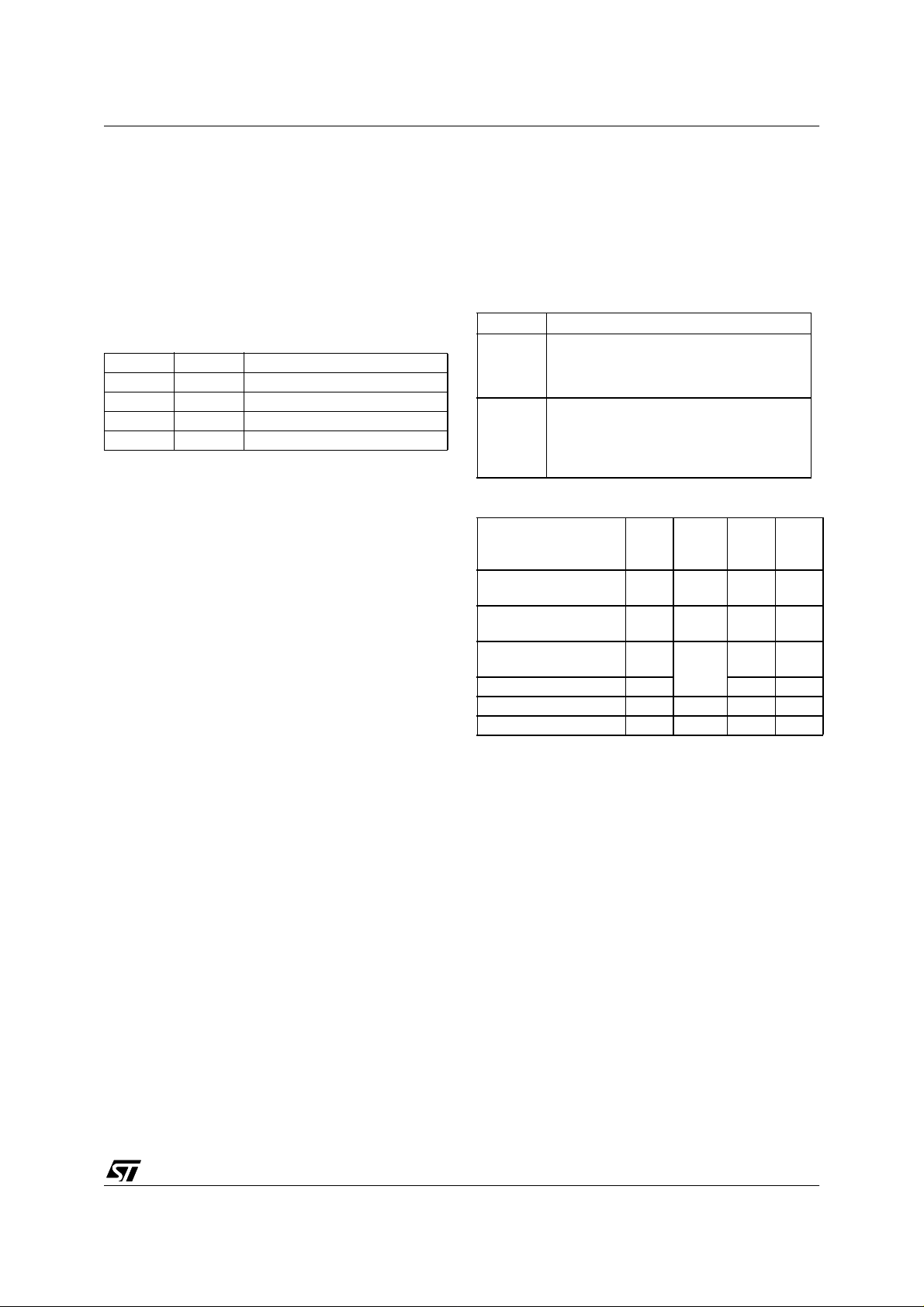
SERIAL COMMUNICATIONS INTERFACE (Cont’d)
11.3.4.6 Parity Control
Parity control (generation of parity bit in trasmission and and parity chec king in recep tion) can b e
enabled by setting the PCE bit in the SCICR1 register. Depending on the frame length defined by
the M bit, the possible SCI frame formats are as
listed in Table 18.
Table 18. Frame Formats
M bit PCE bit SCI Frame
0 0 | SB | 8 bit data | STB |
0 1 | SB | 7-bit data | PB | STB |
1 0 | SB | 9-bit data | STB |
1 1 | SB | 8-bit data PB | STB |
Legend: SB = Start Bit, STB = Sto p Bi t,
PB = Pa ri ty Bit
Note: In case of wake up by an address mark, the
MSB bit of the data is taken into account and not
the parity bit
Even pa rity: the p arity bit is calculated to ob tain
an even number of “1s” inside the frame made of
the 7 or 8 LSB bits (depending on w hether M is
equal to 0 or 1) and the parity bit.
Ex: data=00110101; 4 bits set => parity bit will be
0 if even parity is selected (PS bit = 0).
Odd par it y: t he pari ty bit is calculated to obtain an
odd number of “1s” inside the frame made of the 7
or 8 LSB bits (depending on whether M is equal to
0 or 1) and the parity bit.
Ex: data=00110101; 4 bits set => parity bit will be
1 if odd parity is selected (PS bit = 1).
Transmission mode: If the PCE bit is set then the
MSB bit of the data written in the data register is
not transmitted but is changed by the parity bit.
Reception mode: If the PCE bit is set then the interface checks if the received data byte has an
even number of “1s” if even parity is selected
ST7263B
(PS=0) or an odd number of “1s” if odd parity is selected (PS=1). If the parity check fails, the PE flag
is set in the SCISR register and an interrupt i s generated if PIE is set in the SCICR1 register.
11.3.5 Low Power Modes
Mode Description
No effect on SCI.
WAIT
HALT
11.3.6 Interrupts
Interrupt Event
Transmit Data Register
Empty
Transmission Complete
Received Data Ready
to be Read
Overrun Error Detected OR Yes No
Idle Line Detected IDLE ILIE Yes No
Parity Error PE PIE Yes No
The SCI interrupt events are connected to the
same interrupt vect or .
These events generate an interrupt if the corresponding Enable Control Bit is set and the interrupt mask in the CC register is reset (RIM instruction).
SCI interrupts cause the device to exit
from Wait mode.
SCI registers are frozen.
In Halt mode, the SCI stops transmitting/receiving until Halt mode is exited.
Enable
Event
Control
Flag
TDRE TIE Yes No
TC TCIE Yes No
RDRF
Bit
RIE
Exit
from
Wait
Exit
from
Halt
Yes No
61/132
Page 62

ST7263B
SERIAL COMMUNICATIONS INTERFACE (Cont’d)
11.3.7 Register Description
STATUS REGISTER (SCISR)
Read Only
Reset Value: 1100 0000 (C0h)
70
TDRE TC RDRF IDLE OR NF FE PE
Bit 7 = TDRE
Transmit data register empty.
This bit is set by hardware when the content of the
TDR register has been transferred into the shift
register. An interrupt is generated if the TIE bit=1
in the SCICR2 register. It is cleared b y a sof tw are
sequence (an access to the SCISR register followed by a write to the SCIDR register).
0: Data is not transferred to the shift register
1: Data is transferred to the shift register
Note: Dat a will not be transferred t o the shift register unless the TDRE bit is cleared.
Bit 6 = TC
Transmission complete.
This bit is set by hardware when transmission of a
frame containing Data, a Preamble or a Break is
complete. An interrupt is generat ed if TCIE=1 in
the SCICR2 register. It is cleared by a software sequence (an access to the SCISR register followed
by a write to the SCIDR register).
0: Transmission is not complete
1: Transmission is complete
Bit 5 = R DRF
Received data ready flag.
This bit is set by hardware when the content of the
RDR register has been transferred to the SCI DR
register. An interrupt is generated if RIE=1 in the
SCICR2 register. It is cleared by a software sequence (an access to the SCISR register followed
by a read to the SCIDR register).
0: Data is not received
1: Received data is ready to be read
Bit 4 = IDLE
Idle line detect.
This bit is set by hardware when a I dle Line is detected. An interrupt is generated if the ILIE=1 i n
the SCICR2 register. It is cleared by a software sequence (an access to the SCISR register followed
by a read to the SCIDR register).
0: No Idle Line is detected
1: Idle Line is detected
Note: T he IDLE bit will not b e set again u ntil the
RDRF bit has been set itself (i.e. a new idle line oc-
curs). This bit is not set by an idle line when the receiver wakes up from wake-up mode.
Bit 3 = OR
Overrun error.
This bit is set by hardware when the word currently
being received in the s hift register is ready to be
transferred into the RDR register while RDRF=1.
An interrupt is generated if RIE=1 in the SCICR2
register. It is cleared by a software seque nce (an
access to the SCISR register followed by a read to
the SCIDR register).
0: No Overrun error
1: Overrun error is detected
Note: When this bit is set RDR regi ster content will
not be lost but the shift register will be overwritten.
Bit 2 = NF
Noise flag.
This bit is set by hardware when noise is detected
on a received frame. It is cleared by a software sequence (an access to the SCISR register followed
by a read to the SCIDR register).
0: No noise is detected
1: Noise is detected
Note: This bit does not generate interrupt as it appears at the same time as the RDRF bit which itself generates an interrupt.
Bit 1 = FE
Framing error.
This bit is set by hardware when a de-synchronization, excessive noise or a b reak character is detected. It is cleared by a software sequence (an
access to the SCISR register followed by a read to
the SCIDR register).
0: No Framing error is detected
1: Framing error or break character is detected
Note: This bit does not generate interrupt as it appears at the same time as the RDRF bit which itself generates an interrupt. If the word currently
being transferred causes both frame error and
overrun error, it will be transferred and only the OR
bit will be se t.
Bit 0 = PE
Parity error.
This bit is set by hardware when a parity error occurs in receiver mode . It is cleared by a software
sequence (a read to the status register followed by
an access to the SCIDR da ta register). An interrupt is generated if PIE=1 in the SCICR1 register.
0: No parity error
1: Parity error
62/132
Page 63

SERIAL COMMUNICATIONS INTERFACE (Cont’d)
CONTROL REGISTER 1 (SCICR1)
Read/Write
Reset Value: x000 0000 (x0h)
70
Bit 3 = WAKE
This bit determines the SCI Wake-Up method, it is
set or cleared by software.
0: Idle Line
1: Address Mark
Wake-Up method.
ST7263B
R8 T8 SCID M WAKE PCE PS PIE
Bit 7 = R8
Receive data bit 8.
This bit is used t o store the 9t h bit o f the rec ei ved
word when M=1.
Bit 6 = T8
Transmit data bit 8.
This bit is used to store the 9th bit of the transmitted word when M=1.
Bit 5 = SCID
Disabled for low power consumption
When this bit is set the SCI prescalers and outputs
are stopped and the end of the current byte transfer in order to reduce power consumption.This bit
is set and cleared by software.
0: SCI enabled
1: SCI prescaler and outputs disabled
Bit 4 = M
Word length.
This bit determines the word length. It is set or
cleared by software.
0: 1 Start bit, 8 Data bits, 1 Stop bit
1: 1 Start bit, 9 Data bits, 1 Stop bit
Note: The M bit must not be modified during a data
transfer (both transmission and reception).
Bit 2 = PCE
Parity control enable.
This bit selects the hardware parity control (generation and detection). When the parity control i s enabled, the computed parity is inserted at the MSB
position (9th bit if M=1; 8th bit if M=0) and parity is
checked on the received data. This bit is set and
cleared by software. Once it is set, PCE is active
after the current byte (in reception and in transmission).
0: Parity control disabled
1: Parity control enabled
Bit 1 = PS
Parity selection.
This bit selects the odd or even parity when the
parity generation/detection is enabled (PCE bit
set). It is set and cleared by sof tware. The parity
will be selected after the current byte.
0: Even parity
1: Odd parity
Bit 0 = PIE
Parity interrupt enable.
This bit enables the interrupt capability of the hardware parity control when a parity error is de tected
(PE bit set). It is set and cleared by software.
0: Parity error interrupt disabled
1: Parity error interrupt enabled.
63/132
Page 64

ST7263B
SERIAL COMMUNICATIONS INTERFACE (Cont’d)
CONTROL REGISTER 2 (SCICR2)
Read/Write
Reset Value: 0000 0000 (00h)
70
TIE TCIE RIE ILIE TE RE RWU
Bit 7 = TIE
Transmitter interrupt enable
SBK
.
This bit is set and cleared by software.
0: Interrupt is inhibited
1: An SCI interrupt is generated whenever
TDRE=1 in the SCISR register
Bit 6 = TCIE
Transmission complete interrupt ena-
ble
This bit is set and cleared by software.
0: Interrupt is inhibited
1: An SCI interrupt is generated whenever TC=1 in
the SCISR register
Bit 5 = RIE
Receiver interrupt enable
.
This bit is set and cleared by software.
0: Interrupt is inhibited
1: An SCI interrupt is generated whenever OR=1
or RDRF=1 in the SCISR registe r
Bit 4 = ILIE
Idle line interrupt enable.
This bit is set and cleared by software.
0: Interrupt is inhibited
1: An SCI interrupt is generated whenever IDLE=1
in the SCISR register.
Bit 3 = TE
Transmitter enable.
This bit enables the transmitter and assigns the
TDO pin to the alternate function. It is set and
cleared by software.
0: Transmitter is disabled
1: Transmitter is enabled
Note: During transmission, a “0” pulse on the TE
bit (“0” followed by “1”) sends a preamble after the
current word.
Caution: The TDO pin is free for general purpose
I/O only when the TE and RE bits are both cleared
(or if TE is never set).
Bit 2 = RE
Receiver enable.
This bit enables the receiver. It is set and cleared
by software.
0: Receiver is disabled
1: Receiver is enabled and begins searching for a
start bit
Bit 1 = RWU
Receiver wake-up.
This bit determines if the SCI is in mut e mode or
not. It is set and cleared by so ftware and can be
cleared by hardware when a wake-up sequence is
recognized.
0: Receiver in active mode
1: Receiver in mute mode
Note: Before selecting mute mode (setting the
RWU bit), the SCI must receive some da ta first,
otherwise it cannot function in mute mode with
wakeup by idle line detection.
Bit 0 = SBK
Send break.
This bit set is used to se nd break characters. It is
set and cleared by software.
0: No break character is transmitted
1: Break characters are transmitted
Note: If the SBK bit is set to “1” and then to “0”, the
transmitter will send a BREAK word at the end of
the current word.
64/132
Page 65
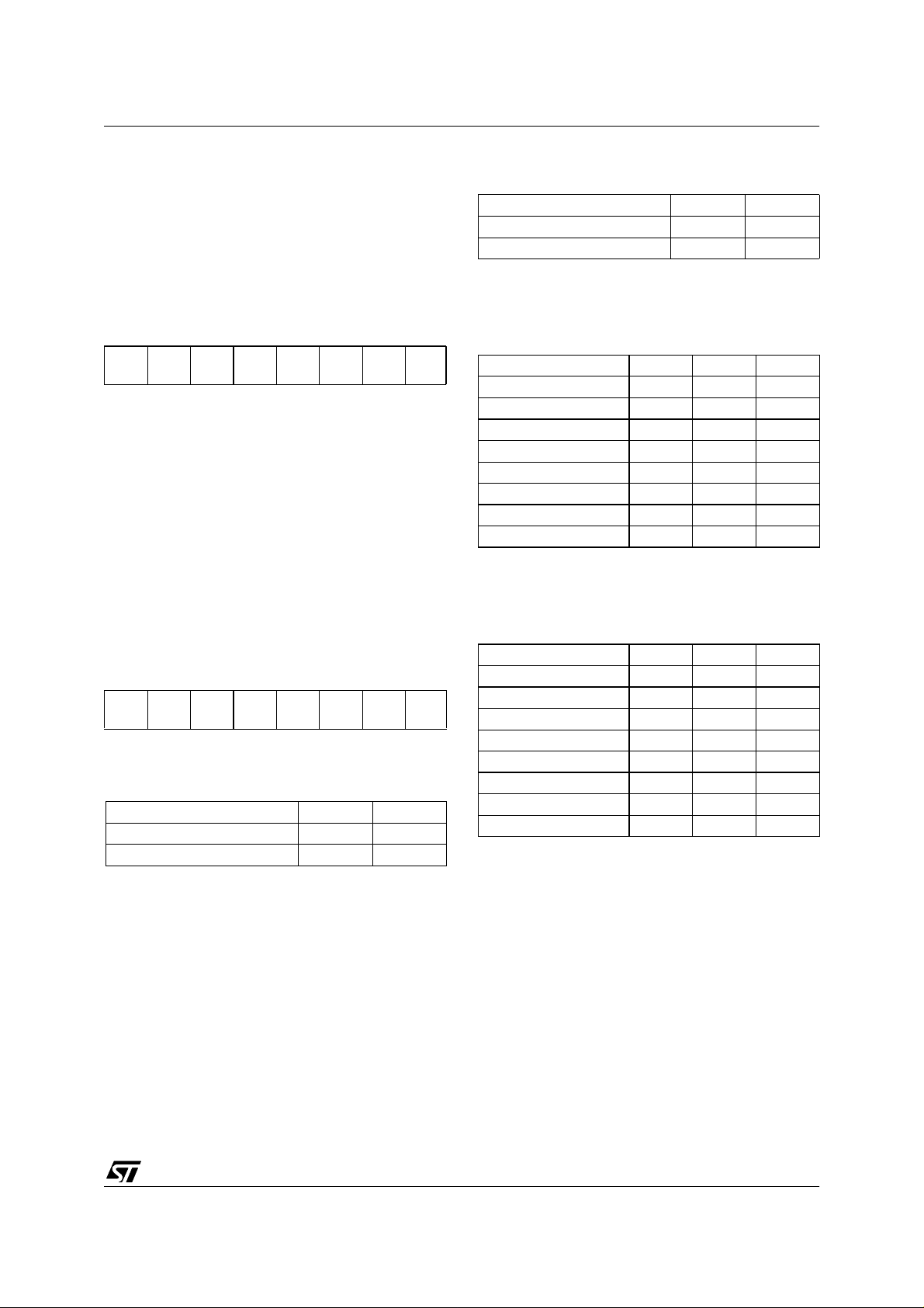
SERIAL COMMUNICATIONS INTERFACE (Cont’d)
DATA REGISTER (SCIDR)
Read/Write
Reset Value: Undefined
PR Prescaling factor SCP1 SCP0
410
13 1 1
Contains the Received or Transmitted dat a character, depending on whether it is read from or written to.
70
Bits 5:3 = SCT[2:0]
SCI Transmitter rate divisor
These 3 bits, in conjunction with the SCP1 & SCP0
bits define the total division applied to the bus
clock to yield the transmit rate clock.
ST7263B
DR7 DR6 DR5 DR4 DR3 DR2 DR1 DR0
The Data register performs a double function (read
and write) since it is composed of two reg is ters,
one for transmission (T DR) and one for recep tion
(RDR).
The TDR register provides the parallel interface
between the internal bus and the out put shift register (see Figure 35).
The RDR register provides the parallel interface
between the input shift register and the internal
TR dividing factor SCT2 SCT1 SCT0
1 000
2 001
4 010
8 011
16 100
32 101
64 110
128 1 1 1
bus (see Fi gure 35).
Bits 2:0 = SCR[2:0]
BAUD RATE REGISTER (SCIBRR)
Read/Write
Reset Value: 0000 0000 (00h)
70
SCP1 SCP0 SCT2 SCT1 SCT0 SCR2 SCR1 SCR0
Bits 7:6= SCP[1:0]
First SCI Prescaler
These 2 prescaling bits allow several standard
clock division ranges:
PR Prescaling factor SCP1 SCP0
100
301
These 3 bits, in conjunc tion with t he SC P[ 1:0 ] bits
define the total division applied to the bus clock to
yield the receive rate clock.
RR dividing factor SCR2 SCR1 SCR0
1 000
2 001
4 010
8 011
16 100
32 101
64 110
128 1 1 1
SCI Receiver rate divisor.
65/132
Page 66
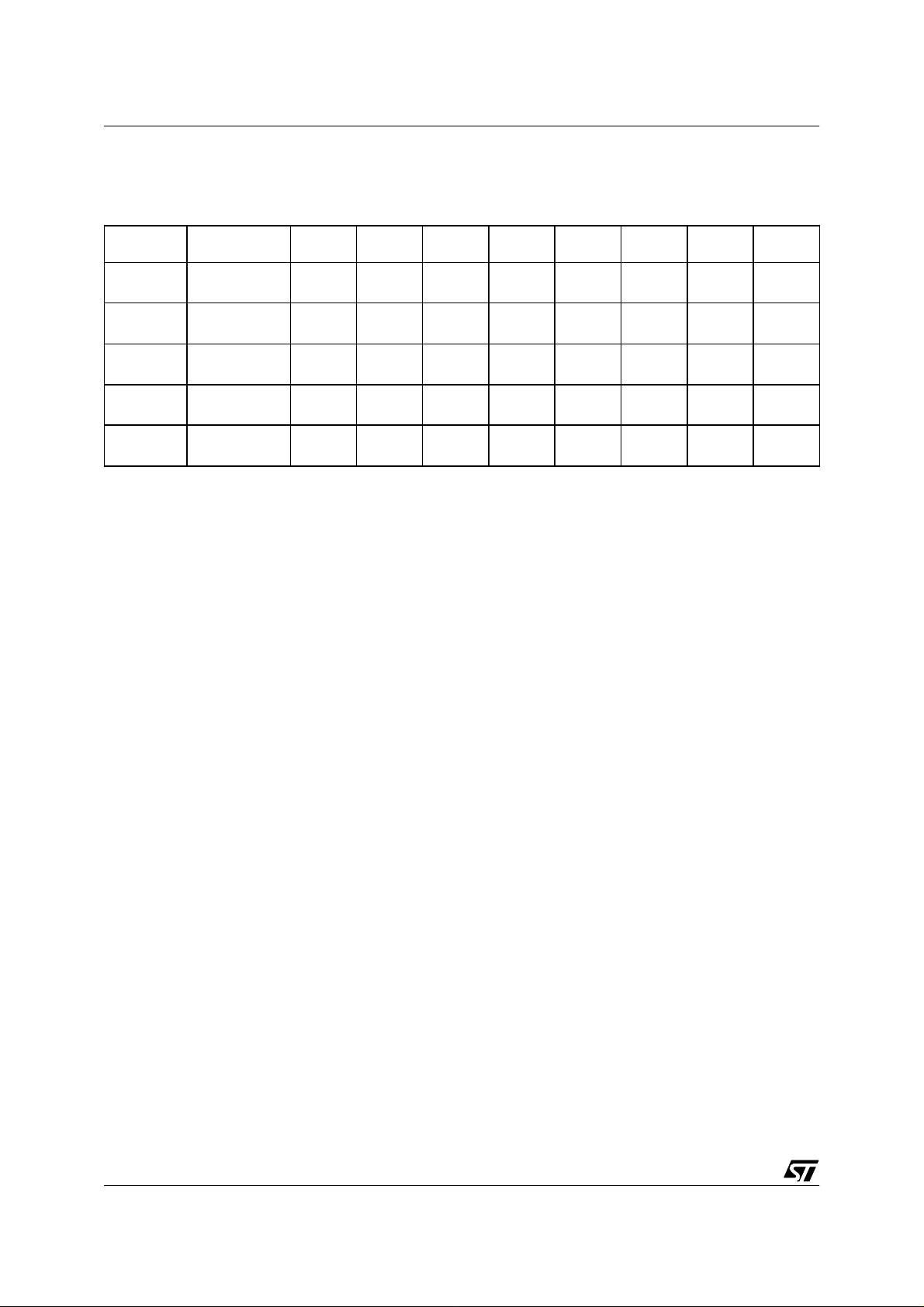
ST7263B
SERIAL COMMUNICATIONS INTERFACE (Cont’d)
Table 19. SCI Register Map and Reset Values
Address
(Hex.)
20 SCISR
21 SCIDR
22 SCIBRR
23 SCICR1
24 SCICR2
Register
Label
Reset Value
Reset Value
Reset Value
Reset Value
Reset Value
76543210
TDRE
1
DR7
x
SCP1
0
R8
x
TIE
0
TC
1
DR6
x
SCP00SCT2xSCT1xSCT0xSCR2xSCR1xSCR0
T8
x
TCIE
0
RDRF0IDLE
0
DR5
x
SCID
0
RIE
0
DR4
x
M
x
ILIE
0
OR
0
DR3
x
WAKE
x
TE
0
NF
0
DR2
x
PCE
0
RE
0
FE
0
DR1
x
PS
0
RWU
0
PE
0
DR0
x
x
PIE
0
SBK
0
66/132
Page 67
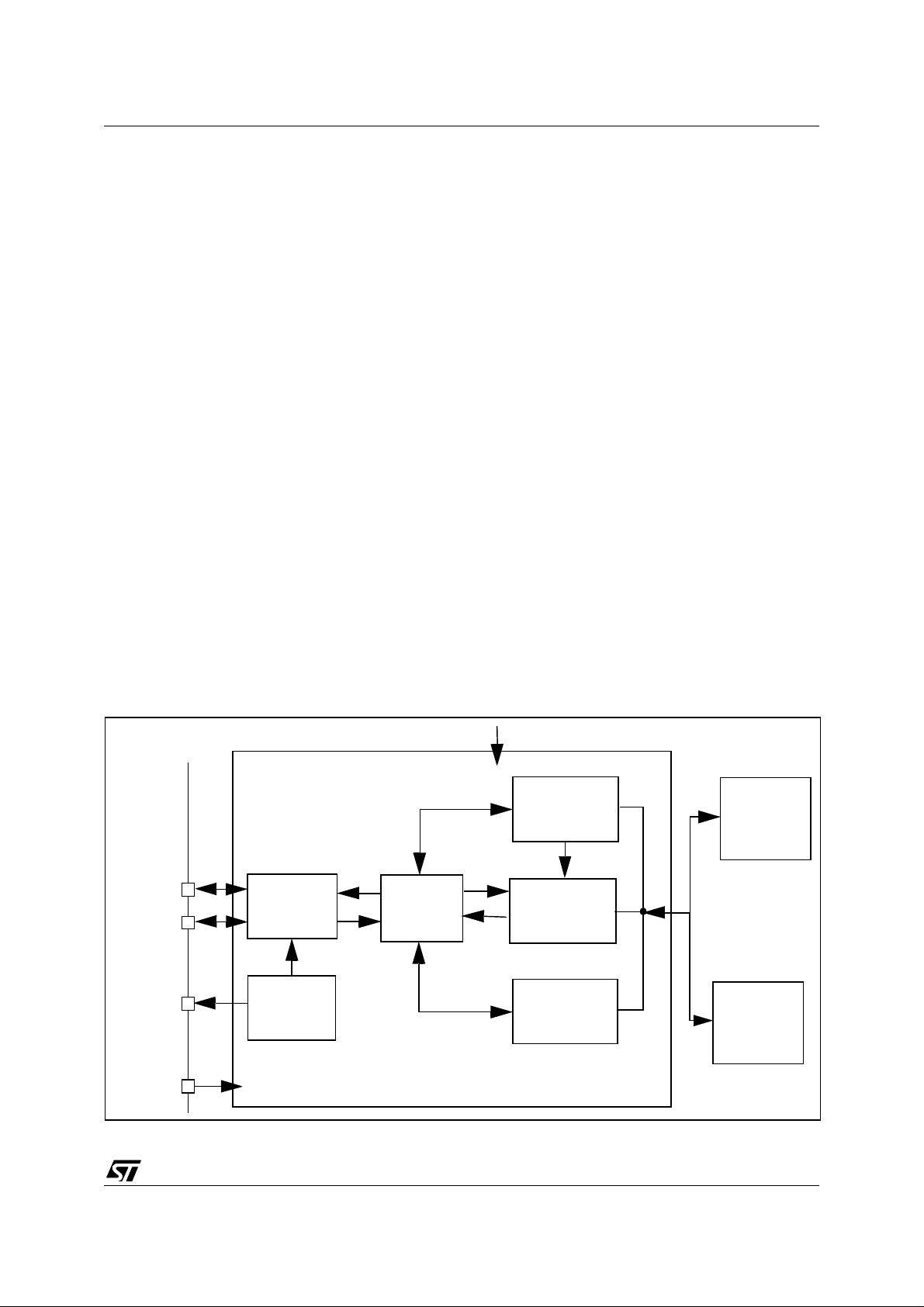
11.4 USB INTERFACE (USB)
ST7263B
11.4.1 Introduction
The USB Interface implements a low-speed function interface between the USB and the ST7 microcontroller. It is a highly integrated circuit whi ch
includes the transceiver, 3.3 voltage regulator, SIE
and DMA. No external components are needed
apart from the external pull-up on USBDM for low
speed recognition by the USB host. The use of
DMA architecture allows the endpoint definition to
be completely flexible. Endpoints can be configured by software as in or out.
11.4.2 Main Features
■ USB Specification Version 1.1 Compliant
■ Supports Low-Speed USB Protocol
■ Two or Three E ndp oint s (i nc luding default one)
depending on the device (see device feature list
and register map)
■ CRC generation/checking, NRZI encoding/
decoding and bit-stuffing
■ USB Suspend/Resume operations
■ DMA Data transfers
■ On-Chip 3.3V Regulator
■ On-Chip USB Transceiver
11.4.3 Functional Description
The block diagram in Figure 37, gives an overview
of the USB interface hardware.
For general information on the USB, refer to the
“Universal Serial Bus Specifications” document
available at http//:www.usb.org.
Serial Interface Engine
The SIE (Serial Interface Engine) interfaces with
the USB, via the transceiver.
The SIE processes tokens, handles data transmission/reception, and handshaking as required by
the USB standard. It also perf orms frame formatting, including CRC generation and checking.
Endpoints
The Endpoint registers indicate if the microcontroller is ready to transmit/receive, and how many
bytes need to be transmitted.
DMA
When a token for a valid Endpoint is recognized by
the USB interface, the related data transfer takes
place, using DMA. At the end of the transaction, an
interrupt is generated.
Interrupts
By reading the Interrupt S ta tus register, application software can know which USB event has occurred.
Figure 37. USB Block Diagram
USBDM
Transceiver
USBDP
3.3V
USBVCC
Voltage
Regulator
USBGND
SIE
6 MHz
ENDPOINT
REGISTERS
DMA
INTERRUPT
REGISTERS
CPU
Address,
data buses
and interrupts
MEMORY
67/132
Page 68
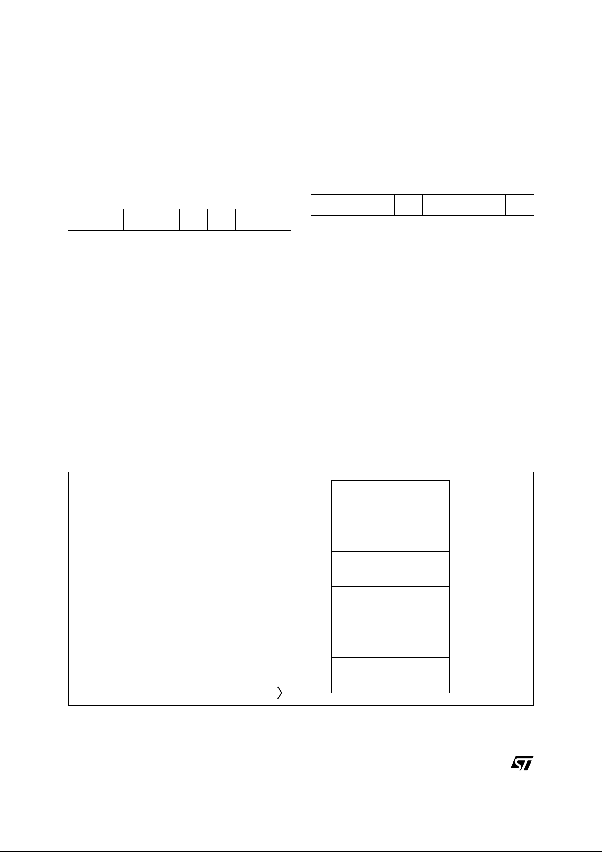
ST7263B
USB INTERFACE (Cont’d)
11.4.4 Register Description
DMA ADDRESS REGISTER (DMAR)
Read / Write
Reset Value: Undefined
70
DA15 DA14 DA13 DA12 DA11 DA10 DA9 DA8
Bits 7:0= DA[15:8]
Software must write the start address of the DMA
memory area whose most significant bits are given
by DA15-DA6. The remaining 6 address bits are
set by hardware. See the description of the I DR
register and Figure 38.
DMA address bits 15-8.
INTERRUPT/DMA REGISTER (IDR)
Read / Write
Reset Value: xxxx 0000 (x0h)
70
DA7 DA6 EP1 EP0 CNT3 CNT2 CNT1 CNT0
Bits 7:6 = DA[7:6]
Software must reset these bits. See the description of the DMAR register and Figure 38.
Bits 5:4 = EP[1:0]
These bits identify the endpoint which required attention.
00: Endpoint 0
01: Endpoint 1
10: Endpoint 2
When a CTR interrupt occurs (see register ISTR)
the software should read the EP bits to identify the
endpoint which has sent or received a packet.
DMA address bits 7-6.
Endpoint numb er
(read-only).
Figure 38. DMA Buffers
DA15-6,000000
Bits 3:0 = CNT[3:0]
This field shows how man y data bytes have b een
received during the last data reception.
Note: Not valid for data transmission.
Byte count
(read only).
101111
Endpoint 2 TX
101000
100111
Endpoint 2 RX
100000
011111
Endpoint 1 TX
011000
010111
Endpoint 1 RX
010000
001111
Endpoint 0 TX
001000
000111
Endpoint 0 RX
000000
68/132
Page 69
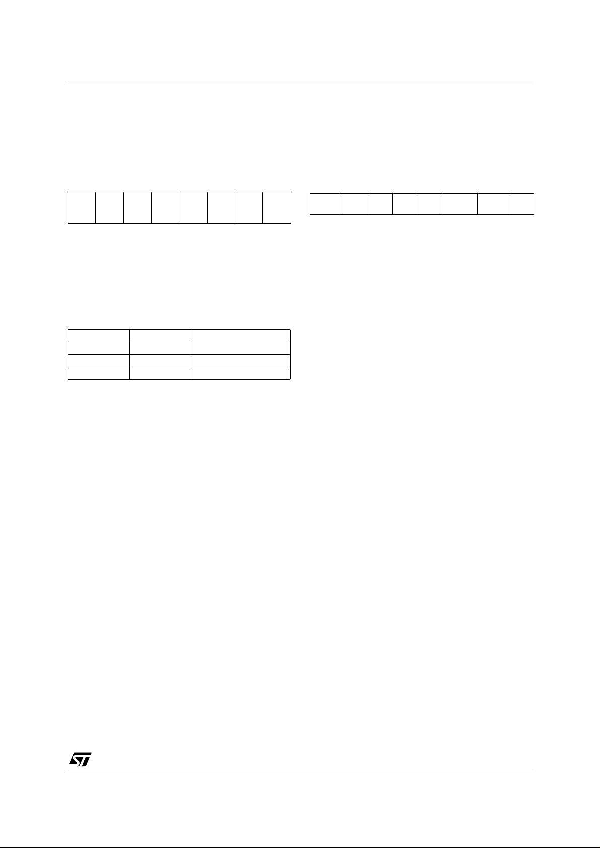
USB INTERFACE (Cont’d)
PID REGISTER (PIDR)
Read only
Reset Value: xx00 0000 (x0h)
ST7263B
INTERRUPT STATUS REGISTER (ISTR)
Read / Write
Reset Value: 0000 0000 (00h)
70
TP3TP2000
RX_
SEZ
RXD 0
70
SUSP DOVR CTR ERR IOVR ESUSP RESET SOF
When an interrupt occurs these bits are set by
Bits 7:6 = TP[3:2]
USB token PIDs are encoded in four bits. TP[3:2]
correspond to the variable token PID bits 3 & 2.
Token PID bits 3 & 2
.
hardware. Software must read them to determine
the interrupt type and clear them after servicing.
Note : These bits cannot be set by software.
Note: PID bits 1 & 0 have a fixed value of 01.
When a CTR interrupt occurs (see register ISTR)
the software should read the TP 3 and TP2 bits to
retrieve the PID name of the token received.
The USB standard defines TP bits as:
TP3 TP 2 PID Name
00 OUT
10 IN
1 1 SE TUP
Bit 7 = SUSP
Suspend mode request
This bit is set by hardware when a constant idle
state is present on the bus line for more than 3 ms,
indicating a suspend m ode reques t from the U SB
bus. The suspend request check is active immediately after each USB reset event and its disabled
by hardware when suspend mode is forced
(FSUSP bit of CTLR register) until the end of
resume sequence.
Bits 5:3 Reserved. Forced by hardware to 0.
DMA over/underrun
Bit 2 = R X_SEZ
Received single-ended zero
This bit indicates the status of the RX_SEZ transceiver output.
0: No SE0 (single-ended zero) state
Bit 6 = DOVR
This bit is set by hardware i f the ST7 processor
can’t answer a DMA request in time.
0: No over/underrun detected
1: Over/underrun detected
1: USB lines are in SE0 (single-ended zero) state
Bit 1 = RXD
Received data
0: No K-state
1: USB lines are in K-state
This bit indicates the status of the RXD transceiver
output (differential receiver output).
Note: If the environment is noisy, the RX_SEZ and
RXD bits can be used to secure the application. By
interpreting the status, software c an distinguish a
valid End Suspend event from a spurious wake-up
due to noise on the external USB line. A valid End
Suspend is followed by a Resume or Reset sequence. A Resume is indicated by RXD=1, a Reset is indicated by RX_SEZ=1.
Bit 5 = CTR
hardware when a correct transfer operation is performed. The type of transfer can be determined by
looking at bits TP3-TP2 in register PIDR. The Endpoint on which the transfer was made is identified
by bits EP1-EP0 in register IDR.
0: No Correct Transfer detected
1: Correct Transfer detected
Note: A transfer where the device sent a NA K or
STALL handshake i s considered not correct (the
host only sends ACK handshak es). A transfer is
considered correct if there are no errors in the PID
and CRC fields, if the DATA0/DATA1 PI D is sent
as expected, if there were no data overruns, bit
stuffing or framing errors.
Correct Transfer.
.
.
This bit is set by
Bit 0 = Reserved. Forced by hardware to 0.
Error.
Bit 4 = ERR
This bit is set by hardware whenever one of the errors listed below has occurred:
0: No error detected
1: Timeout, CRC, bit stuffing or nonstandard
framing error detected
69/132
Page 70
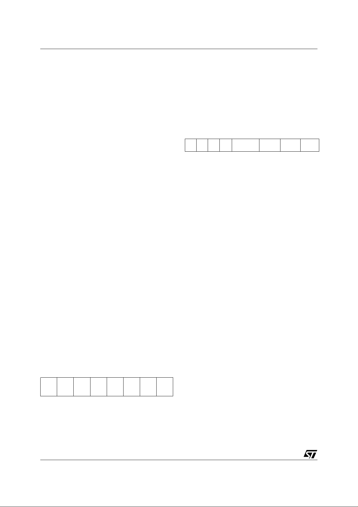
ST7263B
USB INTERFACE (Cont’d)
Bit 3 = IOVR
This bit is set when hardware tries t o set ERR, or
SOF before they have been cleared by software.
0: No overrun detected
1: Overrun detected
Bit 2 = ESUSP
This bit is set by hardware when, during suspend
mode, activity is detected that wakes the USB i nterface up from suspend mode.
This interrupt is serviced by a specific vector, in order to wake up the ST7 from HALT mode.
0: No End Suspend detected
1: End Suspend detected
Interrupt overrun.
End suspend mode
.
of each bit, please refer t o the corresponding bit
description in ISTR.
CONTROL REGISTER (CTLR)
Read / Write
Reset Value: 0000 0110 (06h)
70
0 0 0 0 RESUME PDWN FSUSP FRES
Bits 7:4 = Reserved. Forced by hardware to 0.
Bit 1 = R ESET
USB reset.
This bit is set by hardware when the USB reset sequence is detected on the bus.
0: No USB reset signal detected
1: USB reset signal detected
Note: The DADDR, EP0RA, EP0RB, EP1RA,
EP1RB, EP2RA and EP2RB registers are reset by
a USB reset.
Bit 0 = SOF
Start of frame.
This bit is set by hardware when a low-speed SOF
indication (keep-alive strobe) is seen o n the USB
bus. It is also issued at the end of a resume sequence.
0: No SOF signal detected
1: SOF signal detected
Note: To avoid spurious clearing of some bits, it is
recommended to clear them using a load instruction where all bits which must not be altered are
set, and all bits to be cleared are reset. Avoid readmodify-write instructions like AND , XOR..
INTERRUPT MASK REGISTER (IMR)
Read / Write
Reset Value: 0000 0000 (00h)
Bit 3 = RESUME
Resume
.
This bit is set by software to wake-up the Host
when the ST7 is in suspend mode.
0: Resume signal not forced
1: Resume signal forced on the USB bus.
Software should clear this bit after the appropriate
delay.
Bit 2 = PDWN
Power down
.
This bit is set by software to turn off the 3.3V onchip voltage regulator that supplies the external
pull-up resistor and the transceiver.
0: Voltage regulator on
1: Voltage regulator off
Note: After turning on the voltage regulator, software should allow at le ast 3 µs for s tabilisation of
the power supply before using the USB interface.
Bit 1 = FSUSP
Force suspend mode
.
This bit is set by software to enter Suspend mode.
The ST7 should als o be halted allowing at least
600 ns before issuing the HALT instruction.
0: Suspend mode inactive
1: Suspend mode active
When the hardware detec ts USB a ctivity, it res ets
this bit (it can also be reset by software).
70
SUSPMDOVRMCTRMERRMIOVRMESU
SPM
RES
ETM
SOF
M
Bit 0 = FRES
This bit is set by software to force a reset of the
USB interface, just as if a RESET sequence came
from the USB.
Force reset.
0: Reset not forced
Bits 7:0 = These bits are mask bits for a ll interrupt
condition bits included in the ISTR. Whenever one
of the IMR bits is set, if the corresponding ISTR bit
is set, and the I bit in the CC register is cleared, an
1: USB interface reset forced.
The USB is held in RESET state until software
clears this bit, at which point a “USB-RES ET” interrupt will be generated if enabled.
interrupt request is generated. For an explanation
70/132
Page 71
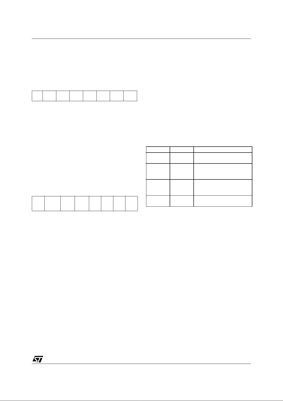
USB INTERFACE (Cont’d)
DEVICE ADDRESS REGISTER (DADDR)
Read / Write
Reset Value: 0000 0000 (00h)
Bit 6 = DTOG_TX
transfers.
It contains the required value of the toggle bit
(0=DATA0, 1=DATA1) for the next transmitted
Data Toggle, for tr ansmission
data packet. This bit is set by hardware at the re-
70
ception of a SETUP P ID. DTOG_TX toggle s only
when the transmitter has received the ACK signal
0 ADD6 ADD5 ADD4 ADD3 AD D2 ADD1 ADD0
from the USB host. DTOG_TX and also
DTOG_RX (see E PnRB ) are n ormal ly up date d by
Bit 7 = Reserved. Forced by hardware to 0.
hardware, at the receipt of a relevant PID. They
can be also written by software.
ST7263B
Bits 6:0 = ADD[6:0]
Software must write into this register the address
sent by the host during enumeration.
Note: This register is also reset when a USB reset
is received from the USB bus or forced through bit
FRES in the CTLR register.
ENDPOINT n REGISTER A (EPnRA)
Read / Write
Reset Value: 0000 xxxx (0xh)
70
ST_
DTOG
OUT
_TX
Device address, 7 bits.
STAT
_TX1
STAT
_TX0
TBC3TBC2TBC1TBC
Bits 5:4 = STAT_TX[1:0]
Status bits, for transmis-
sion transfers.
These bits contain the information about the endpoint status, which are listed below:
STAT_TX1 STAT_TX0 Meaning
00
01
10
11
0
DISABLED: transmission
transfers cannot be executed.
STALL: the endpoint is stalled
and all transmission requests
result in a STALL handshake.
NAK: the endpoint is naked
and all transmission requests
result in a NAK handshake.
VALID: this endpoint is enabled for transmission.
These bits are written by software. Hardware sets
These registers (EP0RA, EP1RA and EP2RA) are
used for controlling data transmission. They are
also reset by the USB bus reset.
Note: Endpoint 2 an d the EP2RA register are not
available on some devices (see device f eature list
the STAT_TX bits to NAK when a correct transfer
has occurred (CTR=1) related to a IN or SETUP
transaction addressed to this endpoint; this allows
the software to prepare the next set of data to be
transmitted.
and register map).
Bit 7 = ST_OUT
Status out.
This bit is set by software to indicate that a status
out packet is expec ted: in this case, all no nzero
OUT data transfers on the endpoint are STALLe d
instead of being ACKed. When ST _OUT is reset,
OUT transactions can have any number of bytes,
as needed.
Bits 3:0 = TBC[3:0]
point n.
Before tr ansmis sion, af ter fillin g the trans mit buf fer, software must write in the TBC field the transmit packet size expressed in bytes (in the range 0-
8).
Warning: Any value outside the range 0-8 will-
induce undesired effects (such as continuous data
transmission).
Transmit byte count for E nd-
71/132
Page 72
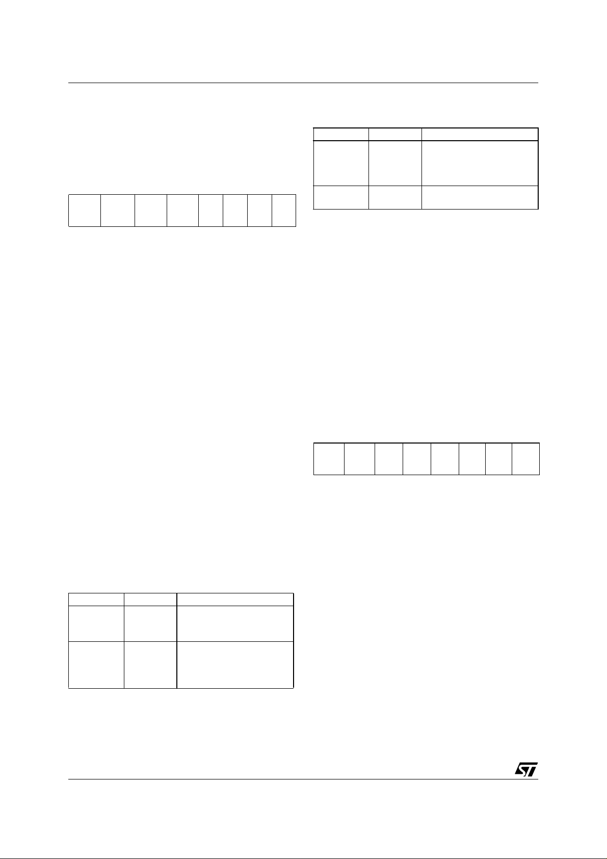
ST7263B
USB INTERFACE (Cont’d)
ENDPOINT n REGISTER B (EPnRB)
Read / Write
Reset Value: 0000 xxxx (0xh)
70
CTRL
DTOG
_RX
STAT
_RX1
STAT
EA3 EA2 EA1 EA0
_RX0
These registers (EP1RB and EP2RB) are used for
controlling data reception on Endpoints 1 and 2.
They are also reset by the USB bus reset.
Note: Endpoint 2 an d the EP2RB register are not
available on some devices (see device f eature list
and register map).
Bit 7 = CTRL
Control.
This bit should be 0.
Note: If this bit is 1, the Endpoint is a con trol e nd-
point. (Endpoint 0 is always a control Endpoint, but
it is possible to have more than one control Endpoint).
Bit 6 = DTOG_RX
fers
.
Data toggle, for reception trans-
It contains the expected value of the toggle bit
(0=DATA0, 1=DATA1) for the next data packet.
This bit is cleared by hardware in the first stage
(Setup Stage) of a control transfer (SETUP transactions start always with DA TA0 PID). The receiver toggles DTOG_RX o nly if it receives a correct
data packet and the packet’s data PID matches
the receiver sequence bit.
STAT_RX1 STAT_RX0 Meaning
NAK: the endpoint is na-
10
ked and all reception requests result in a NAK
handshake.
11
VALID: this endpoint is
enabled for reception.
These bits are written by software. Hardware sets
the STAT_RX bits to NAK wh en a c orrect transfer
has occurred (CTR=1) related to an OUT or SETUP transaction addressed to this endpoint, so the
software has the time to elaborate the received
data before acknowledging a new transaction.
Bits 3:0 = EA[3:0]
Endpoint address
Software must write in this field the 4 -bit address
used to identify the transactions directed to this
endpoint. Usually EP1RB contains “0001” and
EP2RB contains “0010”.
ENDPOINT 0 REGISTER B (EP0RB)
Read / Write
Reset Value: 1000 0000 (80h)
70
DTOGRXSTAT
1
RX1
STAT
RX0
0000
This register is used for controlling data reception
on Endpoint 0. It is also reset b y the USB bus reset.
.
Bits 5:4 = STAT_RX [1:0]
Status bi ts , fo r r ecept ion
transfers.
These bits contain the informat ion abo ut the e ndpoint status, which are listed below:
STAT_RX1 STAT_RX0 Meaning
DISABLED: reception
00
transfers cannot be executed.
STALL: the endpoint is
01
stalled and all reception
requests result in a
STALL handshake.
72/132
Bit 7 = Forced by hardware to 1.
Bits 6:4 = Refer to the EPnRB register for a description of these bits.
Bits 3:0 = Forced by hardware to 0.
Page 73

USB INTERFACE (Cont’d)
11.4.5 Programming Considerations
The interaction between the USB interface and the
application program is described below. Apart
from system reset, action is always initiated by the
USB interface, driven by one of the USB events
associated with the Interrupt Status Register (ISTR) bits.
11.4.5.1 Initializing the Registers
At system reset, t he software must initia lize all registers to enable the USB interface to properly generate interrupts and DMA requests.
1. Initialize the DMAR, IDR, and IMR registers
(choice of enabled interrupts, address of DMA
buffers). Refer the paragraph titled initializing
the DMA Buffers.
2. Initialize the EP0RA and EP0RB registers to
enable accesses to address 0 and endp oint 0
to support USB enumeration. Refer to the paragraph titled Endpoint Initialization.
3. When addresses are received through this
channel, update the content of the DADDR.
4. If needed, write the endpoint numbers in the EA
fields in the EP1RB and EP2RB register.
11.4.5.2 Initializing DMA buffers
The DMA buffers are a contiguous zone of memory whose maximum size is 48 bytes. They can be
placed anywhere in the memory space t o enable
the reception of messages. The 10 most significant bits of the start of this memory area are specified by bits DA15-DA6 in registers DMAR and
IDR, the remaining bits are 0. The memory map is
shown in Figure 38.
Each buffer is filled starting from the bottom (last 3
address bits=000) up.
11.4.5.3 Endpoint Initialization
To be ready to receive:
Set STAT_RX to VALID (11b) in EP0RB to enable
reception.
To be ready to transmit:
1. Write the data in the DMA transmit buffer.
2. In register EPnRA, specify the number of bytes
to be transmitted in the TBC field
3. Enable the endpoint by setting the STAT_TX
bits to VALID (11b) in EPnRA.
Note: Once transmission and/or reception are enabled, registers EPnRA and/or EPnRB (respec-
ST7263B
tively) must not be modified by software, as the
hardware can change their value on the fly.
When the operation is completed, they can be accessed again to enable a new operation.
11.4.5.4 Interrupt Handling
Start of Frame (SOF)
The interrupt service routine may monitor the SOF
events for a 1 ms synchronization event to the
USB bus. This interrupt is ge nerated at the end of
a resume sequence and can also be used to detect this event.
USB Reset (RESET)
When this event occurs, the DADDR register is reset, and communication is disabled i n all en dpoint
registers (the USB interface will not respond to any
packet). Software is responsible for reenabling
endpoint 0 within 10 ms of the end of reset . To do
this, set the STAT_RX bits in the EP0RB register
to VALID.
Suspend (SUSP)
The CPU is warned abou t the lack of bus activity
for more than 3 ms, which i s a suspend request.
The software should set the USB interface to suspend mode and execute an S T 7 HA LT i ns truction
to meet the USB-specified power constraints.
End Suspend (ESUSP)
The CPU is alerted by ac tivity on the US B, which
causes an ESUSP interrupt. The ST7 automatically terminates HALT mode.
Correct Transfer (CTR)
1. When this event occurs, the hardware automatically sets the STAT _ TX or STAT_ RX to NAK.
Note: Every valid endpoint is NAKed until software clears the CTR bit in the ISTR register,
independently of the endpoint number
addressed by the tr ansfer which generated t he
CTR interrupt.
Note: If the event triggering the CTR interrupt is
a SETUP transaction, both STAT_TX and
STAT_RX are set to NAK.
2. Read the PIDR to obtain the token and t he I DR
to get the endpo int number related to t he last
transfer.
Note: When a CTR i nterrupt occurs, the TP3TP2 bits in the P IDR register and EP1-EP0 bi ts
in the IDR register stay unchanged until the
CTR bit in the ISTR register is cleared.
3. Clear the CTR bit in the ISTR register.
73/132
Page 74

ST7263B
USB INTERFACE (Cont’d)
Table 20. USB Register Map and Reset Values
Address
(Hex.)
25
26
27
28
29
2A
2B
2C
2D
2E
2F
30
31
Register
Name
PIDR
Reset Value
DMAR
Reset Value
IDR
Reset Value
ISTR
Reset Value
IMR
Reset Value
CTLR
Reset Value
DADDR
Reset Value
EP0RA
Reset Value
EP0RB
Reset Value
EP1RA
Reset Value
EP1RB
Reset Value
EP2RA
Reset Value
EP2RB
Reset Value
7 6 5 4 3210
TP3
x
DA15
x
DA7
x
SUSP
0
SUSPM0DOVRM
0
0
0
0
ST_OUT
0
1
1
ST_OUT0DTOG_TX0STAT_TX10STAT_TX00TBC3
CTRL0DTOG_RX0STAT_RX10STAT_RX00EA3
ST_OUT0DTOG_TX0STAT_TX10STAT_TX00TBC3
CTRL0DTOG_RX0STAT_RX10STAT_RX00EA3
TP2
x
DA14
x
DA6
x
DOVR
0
0
0
0
ADD6
0
DTOG_TX
0
DTOG_RX0STAT_RX10STAT_RX0
0
0
DA13
x
EP1
x
CTR
0
CTRM
0
0
0
ADD5
0
STAT_TX10STAT_TX00TBC3
0
0
DA12
x
EP0
x
ERR
0
ERRM0IOVRM0ESUSPM0RESETM0SOFM
0
0
ADD4
0
0
0
RX_SEZ0RXD
0
DA11
x
CNT3
0
IOVR0ESUSP0RESET
RESUME0PDWN1FSUSP1FRES
ADD3
0
x
0
0
x
x
x
x
DA10
x
CNT2
0
ADD2
0
TBC2
x
0
0
TBC2
x
EA2
x
TBC2
x
EA2
x
0
DA9
x
CNT1
0
0
ADD1
0
TBC1
x
0
0
TBC1
x
EA1
x
TBC1
x
EA1
x
0
0
DA8
x
CNT0
0
SOF
0
0
0
ADD0
0
TBC0
x
0
0
TBC0
x
EA0
x
TBC0
x
EA0
x
74/132
Page 75
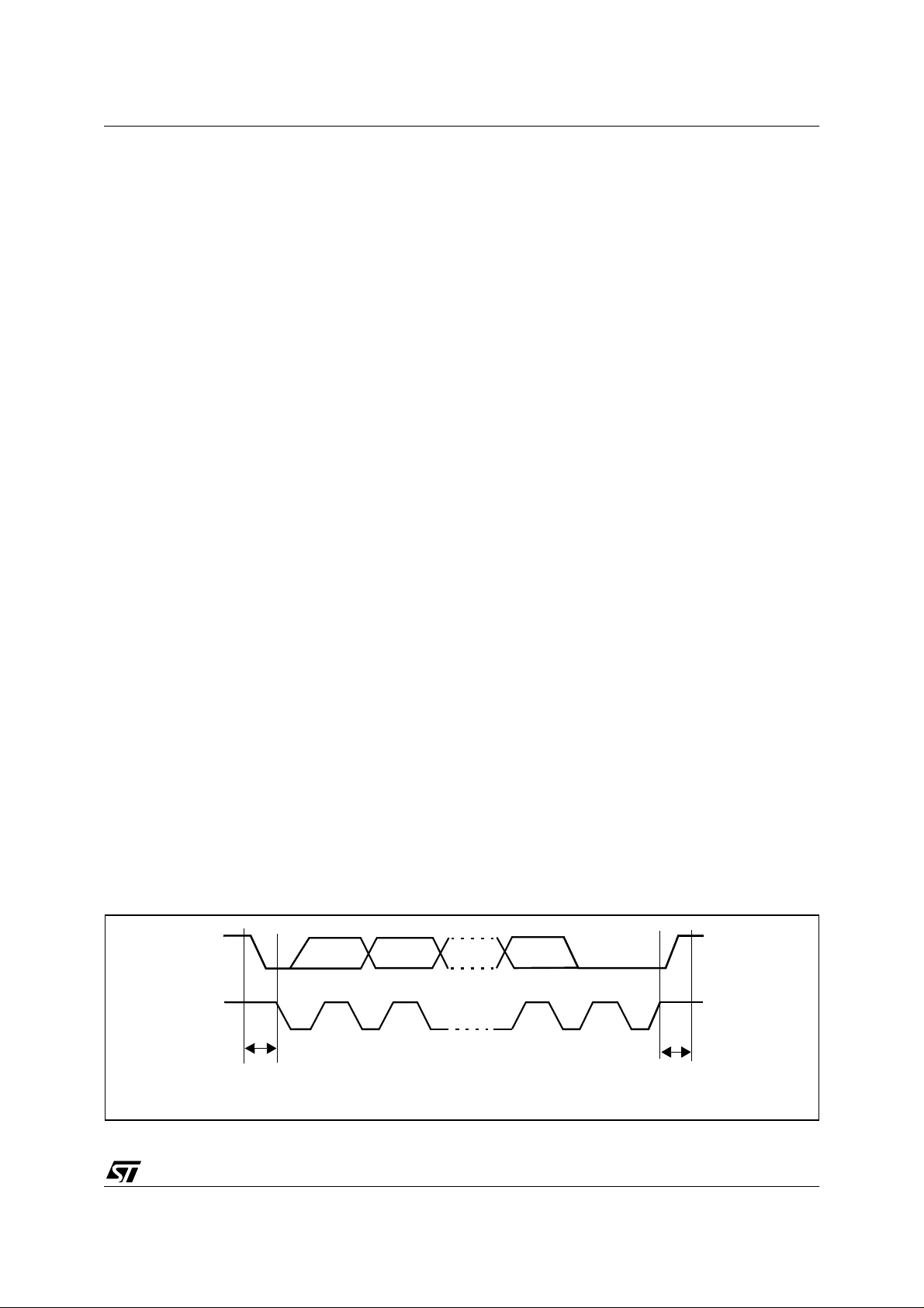
11.5 I²C BUS INTERFACE (I²C)
ST7263B
11.5.1 Introduction
The I²C Bus Interface serves as an in terface between the microcontroller and the serial I²C bus. It
provides both multimaster and slave functions,
and controls all I²C bus-specific sequencing, protocol, arbitration and timing. It supports fast I²C
mode (400 kHz).
11.5.2 Main Features
■ Parallel-bus/I²C protocol converter
■ Multi-master capability
■ 7-bit Addressing
■ Transmitter/Receiver flag
■ End-of-byte transmission flag
■ Transfer problem detection
I²C Master Features:
■ Clock generation
■ I²C bus busy flag
■ Arbitration Lost Flag
■ End of byte transmission flag
■ Transmitter/Receiver Flag
■ Start bit detection flag
■ Start and Stop generation
I²C Slave Features:
■ Stop bit detection
■ I²C bus busy flag
■ Detection of misplaced start or stop condition
■ Programmable I²C Address detection
■ Transfer problem detection
■ End-of-byte transmission flag
■ Transmitter/Receiver flag
11.5.3 General Description
In addition to receiving and transmitting data, this
interface converts it from serial to parallel format
and vice versa, using either an interrupt or polled
handshake. The interrupts are enabled or disabled
by software. The interface is connected to the I²C
bus by a data pin (SDAI) and by a clock pin (SCLI).
It can be connected b oth with a standard I²C bus
and a Fast I²C bus. This selection is made by software.
Mode Selection
The interface can operate in the four following
modes:
– Slave transmitter/receiver
– Master transmitter/receiver
By default, it operates in slave mode.
The interface automatically switches from slave to
master after it generates a START condition and
from master to slave in case of arbitration loss or a
STOP generation, this allows Multi-Master capability.
Communication Flow
In Master mode, it initiates a data transfer and
generates the clock signal. A serial data tran sfer
always begins with a start condition and ends with
a stop condition. Both start and stop conditions are
generated in master mode by software.
In Slave mode, the interface is capable of recognising its own address (7-bit), and the General Call
address. The General Call address d etection may
be enabled or disabled by software.
Data and addresses are transferred as 8-bit bytes,
MSB first. The first byte following the start condition is the address byte; it is al ways transm itted in
Master mode.
A 9th clock pulse follows the 8 clock cycles of a
byte transfer, during which the receiver must send
an acknowledge bit to the transmitter. Refer to Fig -
ure 39.
Figure 39. I²C BUS Protocol
SDA
SCL
START
CONDITION
MSB
ACK
12 89
STOP
CONDITION
VR02119B
75/132
Page 76
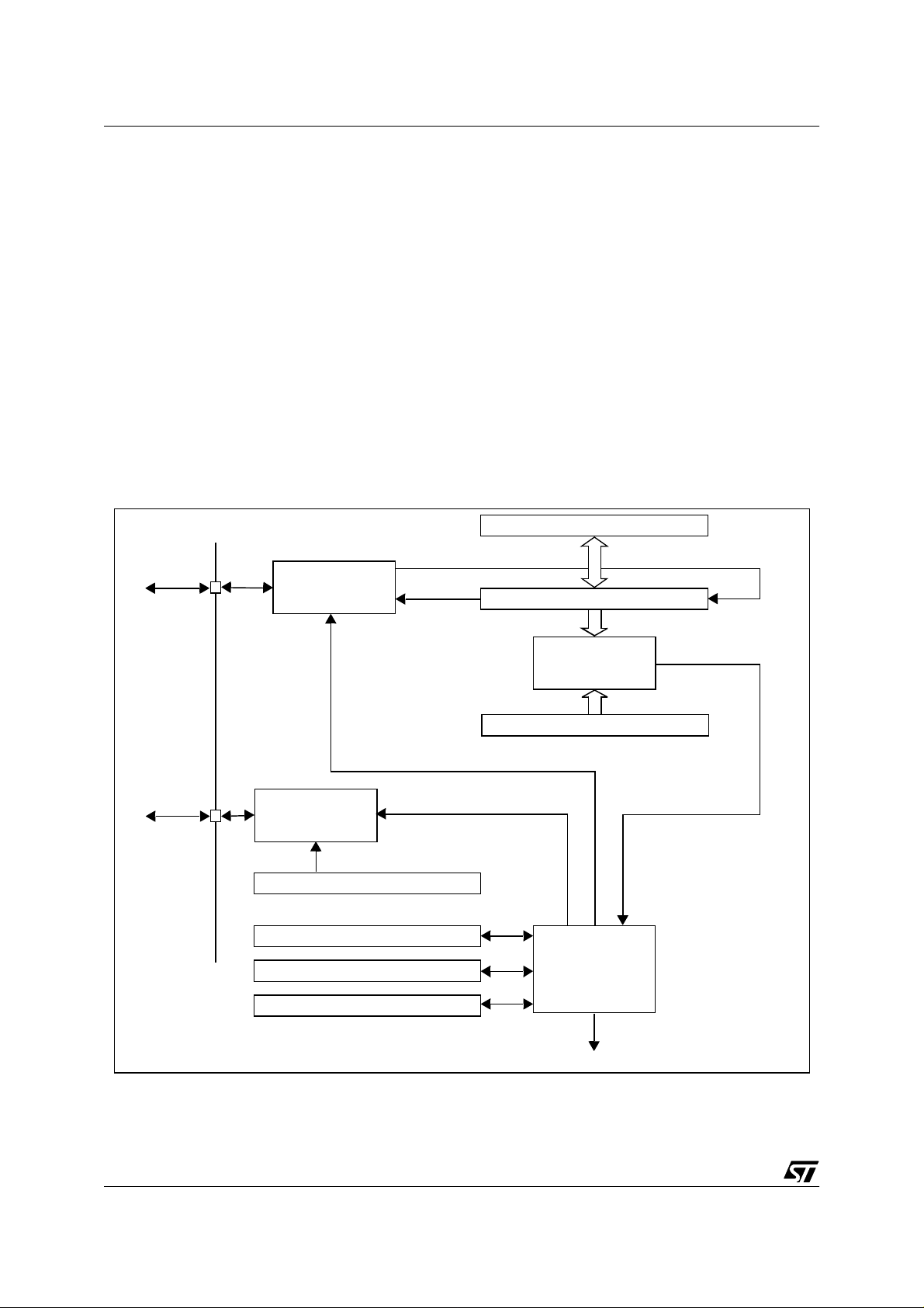
ST7263B
I²C BUS INTERFACE (Cont’d)
The Acknowledge function may be enabled and
disabled by software.
The I²C interface address and/or general call ad-
dress can be selected by software.
The speed of the I²C interface may be selected be-
tween Standard (0-100 kHz) and Fast I²C (100400 kHz).
SDA/SCL Line Control
Transmitter mode: the interface holds the clock
line low before transmission to wait for the microcontroller to write the byte in the Data Register.
Receiver mode: the interface holds the clock line
low after reception to wait for the microcontroller to
read the byte in the Data Register.
Figure 40. I²C Interface Block Diagram
The SCL frequency (F
) is controlled by a pro-
SCL
grammable clock divider which depends on the I²C
bus mode.
When the I²C cell is enabled, the SDA and SCL
ports must be configured as floating open-drain
output or floating input . In this case, the val ue of
the external pull-up resistor used depends on t he
application.
When the I²C cell is disabled, the SDA and SC L
ports revert to being standard I /O port pins.
DATA REG ISTER (DR)
SDA
SCL
SDAI
SCLI
DATA CON TROL
CLOCK CONTROL
CLOCK CONTROL REGIS T ER (CCR)
CONTRO L REGIST ER (CR)
STATUS REGISTER 1 (SR1)
STATUS REGISTER 2 (SR2)
DATA SHIFT REGISTER
COMPARATOR
OWN ADDRESS REGISTER (OAR)
CONTROL LOGIC
76/132
INTERRUPT
Page 77

I²C BUS INTERFACE (Cont’d)
11.5.4 Functional Description
Refer to the CR, SR1 and SR2 registers in Section
11.5.7. for the bit definitions.
By default the I²C interface operates in Slave
mode (M/SL bit is cleared) except when it initiates
a transmit or receive sequence.
11.5.4.1 Slave Mode
As soon as a start condition is detected, the
address is received from the S DA line and s ent to
the shift register; then it is compared with the
address of the interface or the General Call
address (if selected by software).
Address not matched: the interface ignores it
and waits for another Start condition.
Address matched: the interface generates in sequence:
– An A ckno wledge pul se is generated if the ACK
bit is set.
– EVF and ADSL bits are set with an interrupt if the
ITE bit is set.
Then the interface waits for a read of the SR1 register, holding the SCL line low (see Figure 41
Transfer sequencing EV1).
Next, software must read the DR register to determine from the least significant bit if the slave must
enter Receiver or Transmitter mode.
Slave Receiver
Following the address reception and after SR1
register has been read, the slave receives bytes
from the SDA line into the DR register via the internal shift register. After each byte the interface generates in sequence:
– An A ckno wledge pul se is generated if the ACK
bit is set
– EVF and BTF bits are set with an interrupt if the
ITE bit is set.
Then the interface waits for a read of the SR1 register followed by a read of the DR register, holding
the SCL line low (see Figure 41 Transfer se-
quencing EV2).
ST7263B
The slave waits for a read of the SR1 register followed by a write in the DR register, holding the
SCL line low (see Figure 41 Transfer sequencing
EV3).
When the acknowledge pulse is received:
– The EVF and BTF bits are set by hardware with
an interrupt if the ITE bit is set.
Closing Slave Communication
After the last data byte is trans ferred a Sto p Condition is generated by the master. The interface
detects this condition and sets:
– EVF and STOPF bits with an interrupt if the ITE
bit is set.
Then the interface waits for a read of the SR2 register (see Figure 41 Transfer sequencing EV4).
Error Cases
– BERR: Detection of a Stop or a Start condition
during a byte transfer. In this case, the EVF and
BERR bits are set with an interrupt if the ITE bit
is set.
If it is a Stop condition, then the interface discards the data, released the lines and waits for
another Start condition.
If it is a Start condition, then the interface discards the data and waits for the next slave address on the bus.
– AF: Detection of a non-acknowledge bit. In this
case, the EVF and AF bits are set with an interrupt if the ITE bit is set.
Note: In both cases, the S CL line is not held low;
however, the SDA line can remain low due to possible “0” bits transmitted last. It is then necessary
to release both lines by software.
How to Release the SDA / SCL lines
Set and subsequently clear the STOP bit while
BTF is set. The SDA/SC L lines are release d after
the transfer of the current byte.
Slave Transmitter
Following the address reception and after the SR1
register has been read, the slave sends bytes from
the DR regi ster to the SDA line vi a t he internal shift
register.
77/132
Page 78

ST7263B
I²C BUS INTERFACE (Cont’d)
11.5.4.2 Master Mode
To switch from default Slave mode to Master
mode, a Start condition generation is needed.
Start Condition and Transmit Slave Address
Setting the START bit while the BUSY bit is
cleared causes the interface to switch to Master
mode (M/SL bit set) and generates a Start condition.
Once the Start condition is sent:
– The EVF and SB bits are set by hardware with
an interrupt if the ITE bit is set.
Then the master waits for a read of the SR1 register followed by a write in the DR register with the
Slave address byte, holding the SCL line low
(see Figure 41 Transfer sequencing EV5).
Then the slave address byte is sent to the SDA
line via the internal shift register.
After completion of this transfer (and acknowledge
from the slave if the ACK bit is set):
– The EVF bit is set by hardware with interrupt
generation if the ITE bit is set.
Then the master waits for a read of the SR1 register followed by a write in t he CR register (f or example set PE bit), holding the SCL line low (see Fig-
ure 41 Transfer sequencing EV6).
Next the master must enter Rec eiver or Transm itter mode.
Master Receiver
Following the address transmission and after the
SR1 and CR registers have be en accessed, the
master receives bytes from the S DA line into the
DR register via the internal shift register. After
each byte the interface generates in sequence:
– An Acknowledge pulse is generated if if the ACK
bit is set
– EVF and BTF bits are set by hardware with an in-
terrupt if the ITE bit is set.
Then the interface waits for a read of the SR1 register followed by a read of the DR register, holding
the SCL line low (see Figure 41 Transfer se-
quencing EV7).
To close the communication: before reading the
last byte from the DR register, set the STOP bit to
generate the Stop condition . The interfa ce returns
automatically to slave mode (M/SL bit cleared).
Note: In order to gene ra te the non-acknowledge
pulse after the last received data byte, the ACK bit
must be cleared just before reading the second
last data byte.
Master Transmitter
Following the address transmission and after SR1
register has been read, the master sends bytes
from the DR register to the SDA line via the internal shift register.
The master waits for a read of the SR1 register followed by a write in the DR register, holding the
SCL line low (see Figure 41 Transfer sequencing
EV8).
When the acknowledge bit is received, the
interface sets:
– EVF and BTF bits with an interrupt if the ITE bit
is set.
To close the communication: after writing the last
byte to the DR register, set the STOP bit to generate the Stop c ondition. The interface goes automatically back to slave mode (M/SL bit cleared).
Error Cases
– BERR: Detection of a Stop or a Start condition
during a byte transfer. In this case, the EVF and
BERR bits are set by hardware with an interrupt
if the ITE bit is set.
– AF: Detection of a non-acknowledge bit. In this
case, the EVF and AF bits are set by hardware
with a n in terru p t i f the IT E bit is set. To resume ,
set the START or STOP bit.
– ARLO: Detection of an arbitration lost condition.
In this case the ARLO bit is set by hardware (with
an interrupt if the ITE bit is set and the interface
goes automatically back to slave mode (the M/SL
bit is cleared).
Note: In all these cases, the SCL line is not held
low; however, the SDA line can remain low due to
possible “0” bits transmitted last. It is then necessary to release both lines by software.
78/132
Page 79
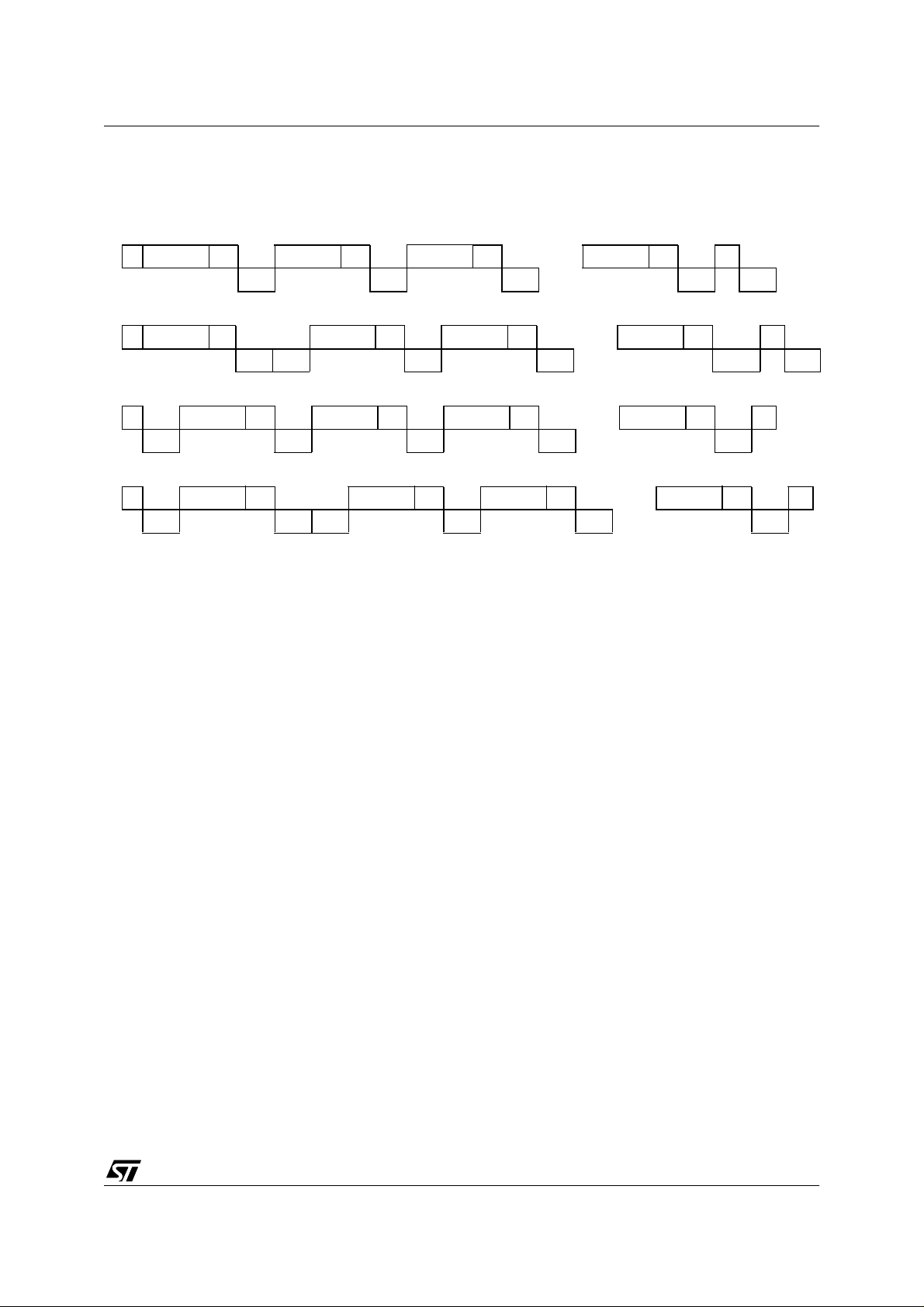
I²C BUS INTERFACE (Cont’d)
Sl
Figure 41. Transfer Sequencing
ave Receiver
S Address A Data1 A Data2 A
EV1 EV2 EV2 EV2 EV4
DataN A P
.....
Slave Transmitter
S Address A Data1 A Data2 A
EV1 EV3 EV3 EV3 EV3-1 EV4
DataN NA P
.....
Master Receiver
S Address A Data1 A Data2 A
EV5 EV6 EV7 EV7 EV7
DataN NA P
.....
Master Transmitter
S Address A Data1 A Data2 A
EV5 EV6 EV8 EV8 EV8 EV8
DataN A P
.....
ST7263B
Legend:
S=Start, P=Stop, A=Acknowledge, NA=Non-acknowledge
EVx=Event (with interrupt if ITE=1)
EV1: EVF=1, ADSL=1, cleared by reading the SR1 register.
EV2: EVF=1, BTF=1, cleared by reading the SR1 register followed by reading the DR register.
EV3: EVF=1, BTF=1, cleared by reading the SR1 register followed by writing the DR register.
EV3-1: EVF=1, AF=1, BTF=1; AF is cleared by reading the SR1 register. The BTF is cleared
by releasing the lines (STOP=1, STOP=0) or by writing the DR register (DR=FFh).
Note: If lines are released by STOP=1, STOP=0, the subsequent EV4 is not seen.
EV4: EVF=1, STOPF=1, cleared by reading the SR2 register.
EV5: EVF=1, SB=1, cleared by reading the SR1 register followed by writing the DR register.
EV6: EVF=1, cleared by reading the SR1 register followed by writing the CR register
(for example PE=1).
EV7: EVF=1, BTF=1, cleared by reading the SR1 register followed by reading the DR register.
EV8: EVF=1, BTF=1, cleared by reading the SR1 register followed by writing the DR register.
79/132
Page 80
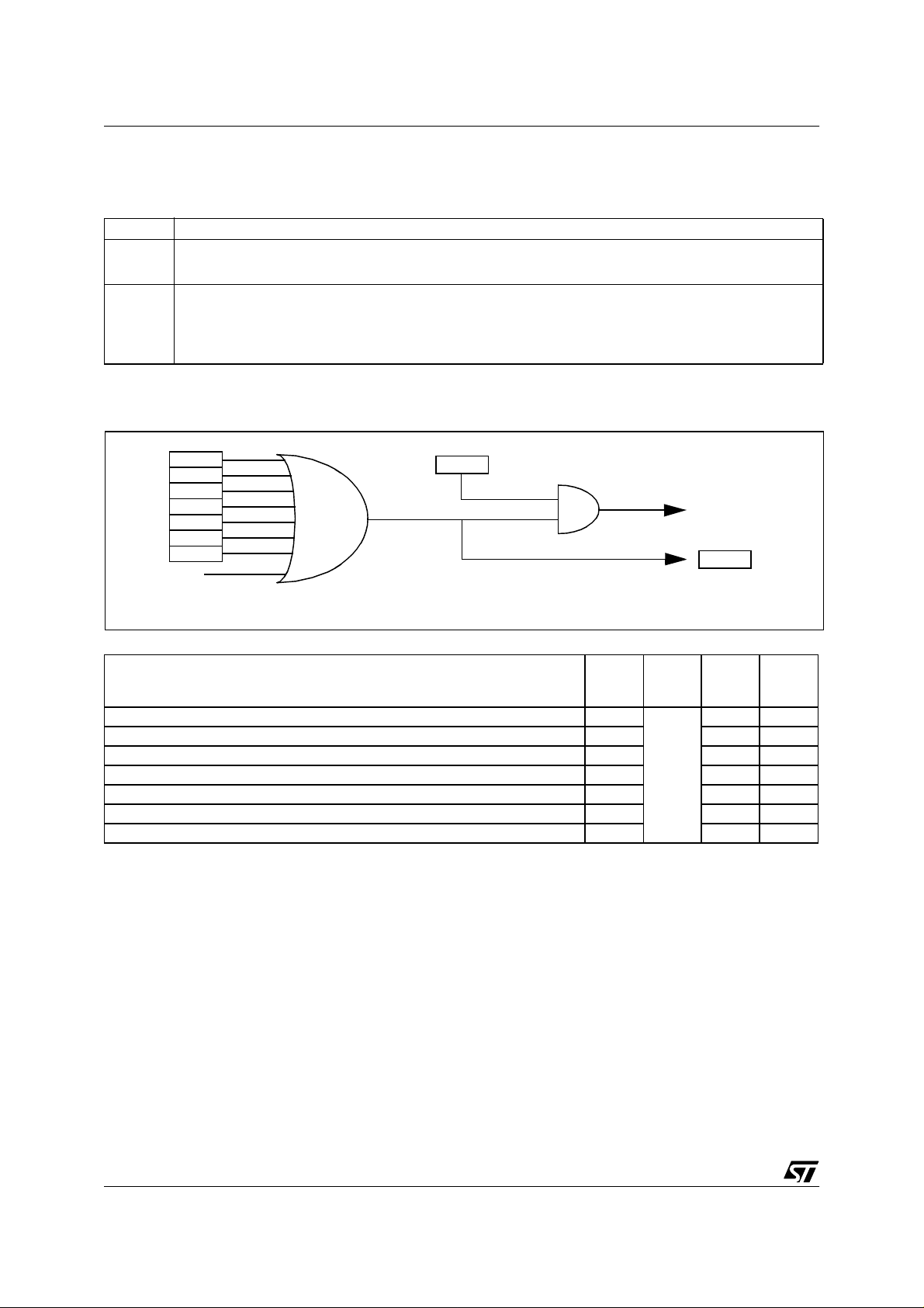
ST7263B
I²C BUS INTERFACE (Cont’d)
11.5.5 Low Power Modes
Mode Description
WAIT
HALT
11.5.6 Interrupts
Figure 42. Event Flags and Interrupt Generation
No effect on I²C interface.
I²C interrupts exit from Wait mode.
I²C registers are frozen.
In Halt mode, the I ²C in terface is inact ive and does not ack nowled ge da ta on the bus. The I²C
interface resumes operation when the MCU is woken up by an interrupt with “exit from Halt
mode” capability.
BTF
ADSL
SB
AF
STOPF
ARLO
BERR
ITE
INTERRUPT
EVF
*
*
EVF can also be set by EV6 or an error from the SR2 register.
Interrupt Event
End of Byte Transfer Event BTF
Address Matched Event (Slave mode) ADSEL Yes No
Start Bit Generation Event (Master mode) SB Yes No
Acknowledge Failure Event AF Yes No
Stop Detection Event (Slave mode) STOPF Yes No
Arbitration Lost Event (Multimaster configuration) ARLO Yes No
Bus Error Event BERR Yes No
The I²C interrupt events are connected to the
same interrupt vector (see Interrupts chapter).
They generate an interrupt if the corresponding
Enable Control Bit is set and the I-bit in the CC
Event
Flag
Enable
Control
Bit
ITE
Exit
from
Wait
Yes No
Exit
from
Halt
register is reset (RIM instruction).
80/132
Page 81

I²C BUS INTERFACE (Cont’d)
11.5.7 Register Description
I²C CONTROL REGISTER (CR)
Read / Write
Reset Value: 0000 0000 (00h)
70
Bit 2 = ACK
This bit is set and cleared by software. It is also
cleared by hardware when the interface is disabled (PE=0).
0: No acknowledge returned
Acknowledge enable.
1: Acknowledge returned after an address byte or
0 0 PE ENGC START ACK STOP ITE
a data byte is received
ST7263B
Bits 7:6 = Reserved. Forced to 0 by hardware.
Bit 5 = PE
Peripheral enable.
This bit is set and cleared by software.
0: Peripheral disabled
1: Master/Slave capability
Notes:
– W hen PE= 0, all the bits of the CR register and
the SR register except the Stop bit are reset. All
outputs are released while PE=0
– W hen PE= 1, the correspond ing I/O pins are se-
lected by hardware as alternate functions.
– To enable the I²C interface, write the CR register
TWICE with PE=1 as the first write only activates
the interface (only PE is set).
Bit 4 = ENGC
Enable General Call.
This bit is set and cleared by software. It is also
cleared by hardware when the interface is disabled (PE=0). The 00h General Call address is acknowledged (01h ignored).
0: General Call disabled
1: General Call enabled
Bit 3 = START
Generation of a Start condition
This bit is set and cleared by software. It is also
cleared by hardware when the interface is disabled (PE=0) or when the Start condition is sent
(with interrupt generation if ITE=1).
– In master mode :
0: No start generation
1: Repeated start generation
– In slave mode :
0: No start generation
1: Start generation when the bus is free
Bit 1 = STOP
Generation of a Stop condition
This bit is set and cleared by software. It is also
cleared by hardware in master mode. Note: This
bit is not cleared when the interface is disabled
(PE=0).
– In Master mode:
0: No stop generation
1: Stop generation after the current byte transfer
or after the current Start condition is sent. The
STOP bit is cleared by hardware when the Stop
condition is sent.
– In Slave mode:
0: No stop generation
1: Release the SCL and SDA lines after the current byte transfer (BTF=1). In this mode the
STOP bit has to be cleared by software.
Bit 0 = ITE
Interrupt enable.
This bit is set and cleared by software and cleared
by hardware when the interface is disabled
(PE=0).
0: Interrupts disabled
1: Interrupts enabled
Refer to Figure 42 for the relationship between the
events and the interrupt.
.
SCL is held low when the SB, BTF or ADS L flags
or an EV6 event (See Figure 41) is detected.
.
81/132
Page 82

ST7263B
I²C BUS INTERFACE (Cont’d)
I²C STATUS REGISTER 1 (SR1)
Read Only
Reset Value: 0000 0000 (00h)
70
EVF 0 TRA BUSY BTF ADSL M/SL SB
Bit 3 = BTF
This bit is set by hardware as soon as a byte is correctly received or transmitted with interrupt generation if ITE=1. It is cleared by software reading
SR1 register followed by a read or write of DR register. It is also cleared by hardware when the interface is disabled (PE=0).
– Following a byte transmission, this bit is set after
Bit 7 = EVF
Event flag.
This bit is set by hardware as soon as an event occurs. It is cleared by software reading SR2 register
in case of error event or as described in Figure 41.
It is also cleared by hardware when the interface is
disabled (PE=0).
0: No event
1: One of the following events has occurred:
– BTF=1 (Byte received or transmitted)
– ADSL=1 (Address matched in Slave mode
while ACK=1 )
– SB=1 (Start condition generated in Master
reception of the acknowledge clock pulse. In
case an address byte is sent, this bit is set only
after the EV6 event (See Figure 41). B TF is
cleared by reading SR1 register followed by writing the next byte in DR register.
– Following a byte reception, this bit is set after
transmission of the acknowledge clock pulse if
ACK=1. BTF is cleared by reading SR1 register
followed by reading the byte from DR register.
The SCL line is held low while BTF=1.
0: Byte transfer not done
1: Byte transfer succeeded
mode)
– AF=1 (No acknowledge received after byte
transmission)
– STOPF=1 (Stop condition detected in Slave
mode)
– ARLO=1 (Arbitration lost in Master mode)
– BERR=1 (Bus error, misplaced Start or Stop
condition detected)
– Address byte successfully transmitted in Mas-
ter mode.
Bit 2 = ADSL
This bit is set by hardware as soon as the received
slave address matched with the OAR register content or a general call is recognized. A n in terrupt is
generated if ITE=1. It is c leared by sof tware reading SR1 register or by hardware when t he in terface is disabled (PE=0).
The SCL line is held low while ADSL=1.
0: Address mismatched or not received
1: Received address matched
Byte transfer finished.
Address matched (Slave mode).
Bit 6 = Reserved. Forced to 0 by hardware.
Bit 5 = TRA
Transmitter/Receiver.
When BTF is set, TRA=1 if a dat a byte has been
transmitted. It is cleared automatically when BTF
is cleared. It is also cleared by hardware after detection of Stop condition (STOPF=1), loss of bus
arbitration (ARLO=1) or when the interface is disabled (PE=0).
0: Data byte received (if BTF=1)
1: Data b yte transmitted
Bit 4 = BUSY
Bus busy
.
This bit is set by hardware on de tection of a S tart
condition and cleared by hardware on detection of
a Stop condition. I t indicates a communi cation in
progress on the bus. This information is still updated when the interface is disabled (PE=0).
0: No communication on the bus
1: Communication ongoing on the bus
82/132
Bit 1 = M/SL
Master/Slave.
This bit is set by hardware as soon as the interface
is in Master mode (writing START=1). It is cleared
by hardware after detecting a Stop condition on
the bus or a loss of arbitration (ARLO=1). It is also
cleared when the interface is disabled (PE=0).
0: Slave mode
1: Master mode
Bit 0 = SB
Start bit (Master mode).
This bit is set by hardware as soon as the Start
condition is generated (following a write
START=1). An interrupt is generated if ITE=1. It is
cleared by software reading SR1 register followed
by writing the address byte in DR register. It is al so
cleared by hardware when the interface is disabled (PE=0).
0: No Start condition
1: Start condition generated
Page 83

I²C BUS INTERFACE (Cont’d)
I²C STATUS REGISTER 2 (SR2)
Read Only
Reset Value: 0000 0000 (00h)
70
es the arbitration of the bus to another master. An
interrupt is generated if ITE=1. It is cleared by software reading SR2 register or by hardware when
the interface is disabled (PE=0).
After an ARLO event the interface switches back
0 0 0 AF STO PF ARLO BERR GCAL
automatically to Slave mode (M/SL=0).
The SCL line is not held low while ARLO=1.
0: No arbitration lost detected
Bits 7:5 = Reserved. Forced to 0 by hardware.
1: Arbitration lost detected
ST7263B
Bit 4 = AF
Acknowledge failure
.
This bit is set by hardware when no acknowledg e
is returned. An interrupt is generated if ITE=1. It is
cleared by software reading SR2 register or by
hardware when the interface is disabled (PE=0).
The SCL line is not held low while AF=1.
0: No acknowledge failure
1: Acknowledge failure
Bit 3 = STOPF
Stop detection (Slave mode).
This bit is set by hardware when a St op condition
is detected on the bus after an acknowledge (if
ACK=1). An interrupt is generated if ITE=1. It is
cleared by software reading SR2 register or by
hardware when the interface is disabled (PE=0).
The SCL line is not held low while STOPF=1.
0: No Stop condition detected
1: Stop condition detected
Bit 2 = ARLO
Arbitration lost
.
This bit is set by hardware when the interface los-
Bit 1 = BERR
Bus error.
This bit is set by hardware when the interface detects a misplaced Start or Stop condition. An interrupt is generated if ITE=1. It is cleared by software
reading SR2 register or by hardware when the interface is disabled (PE=0).
The SCL line is not held low while BERR=1.
0: No misplaced Start or Stop condition
1: Misplaced Start or Stop condition
Bit 0 = GCAL
General Call (Slave mode).
This bit is set by hardware when a general call address is detected on the bu s while ENGC= 1. It is
cleared by hardware detecting a Stop condition
(STOPF=1) or when the interface is disabled
(PE=0).
0: No general call address detected on bus
1: general call address detected on bus
83/132
Page 84
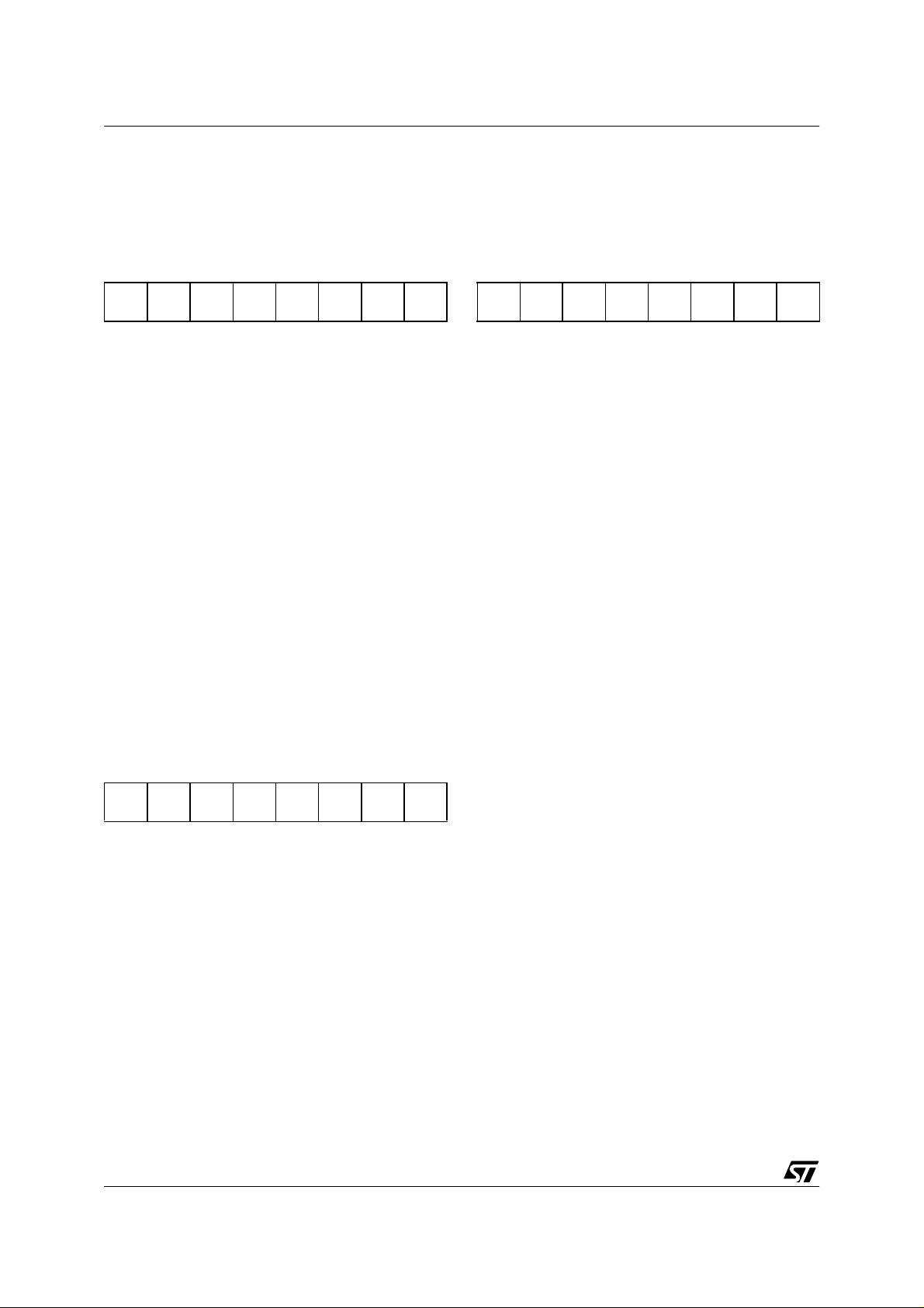
ST7263B
I²C BUS INTERFACE (Cont’d)
I²C CLOCK CONTROL REGISTER (CCR)
Read / Write
Reset Value: 0000 0000 (00h)
I²C OWN ADDRESS REGISTER (OAR)
Read / Write
Reset Value: 0000 0000 (00h)
70
FM/SM CC6 CC5 CC4 CC3 CC2 CC1 CC0
Bit 7 = FM/SM
Fast/Standard I²C mode.
This bit is set and cleared by software. It is not
cleared when the interface is disabled (PE=0).
0: Standard I²C mode
1: Fast I²C mode
Bits 6:0 = CC6-CC0
These bits select the s peed of t he bus (F
7-bit clock divider.
) de-
SCL
pending on the I²C mode. They are not cleared
when the interface is disabled (PE=0).
– St andard m ode (FM /SM=0): F
F
= f
SCL
– Fas t mode (FM /SM =1): F
F
= f
SCL
Note: The programmed F
/(2x([CC6..CC0]+ 2))
CPU
SCL
/(3x([CC6..CC0]+ 2))
CPU
SCL
<= 100kHz
SCL
> 100kHz
assumes no load on
70
ADD7 ADD6 ADD5 ADD4 ADD3 ADD2 ADD1 ADD0
Bits 7:1 = ADD7-ADD1
Interface address
These bits define the I²C bus add ress o f the in terface. They a re not cleared when the interface is
disabled (PE=0).
Bit 0 = ADD0
Address direction bit.
This bit is don’t care, the interface ack nowledges
either 0 or 1. It is not cleared when the interface is
disabled (PE=0).
Note: Address 01h is always ignored.
SCL and SDA lines.
I²C DATA REGISTER (DR)
Read / Write
Reset Value: 0000 0000 (00h)
.
70
D7 D6 D5 D4 D3 D2 D1 D0
Bits 7:0 = D7-D0
8-bit Data Register.
These bits contains the byte to be received or
transmitted on the bus.
– Tr ansmi tter mode: Byte transmiss ion start auto-
matically when the software writes in the DR register.
– Receiver mode: the first data byte is received au-
tomatically in the DR register using the least significant bit of the address.
Then, the next data bytes are received one by
one after reading the DR register.
84/132
Page 85

Table 21. I²C Register Map
Address
(Hex.)
39 DR DR7 .. DR0
3B OAR ADD7 .. ADD0
3C CCR FM/SM CC6 .. CC0
3D SR2 AF STOPF ARLO BERR GCAL
3E SR1 EVF TRA BUSY BTF ADSL M/SL SB
3F CR PE ENGC START ACK STOP ITE
Register
Name
7654 3210
ST7263B
85/132
Page 86
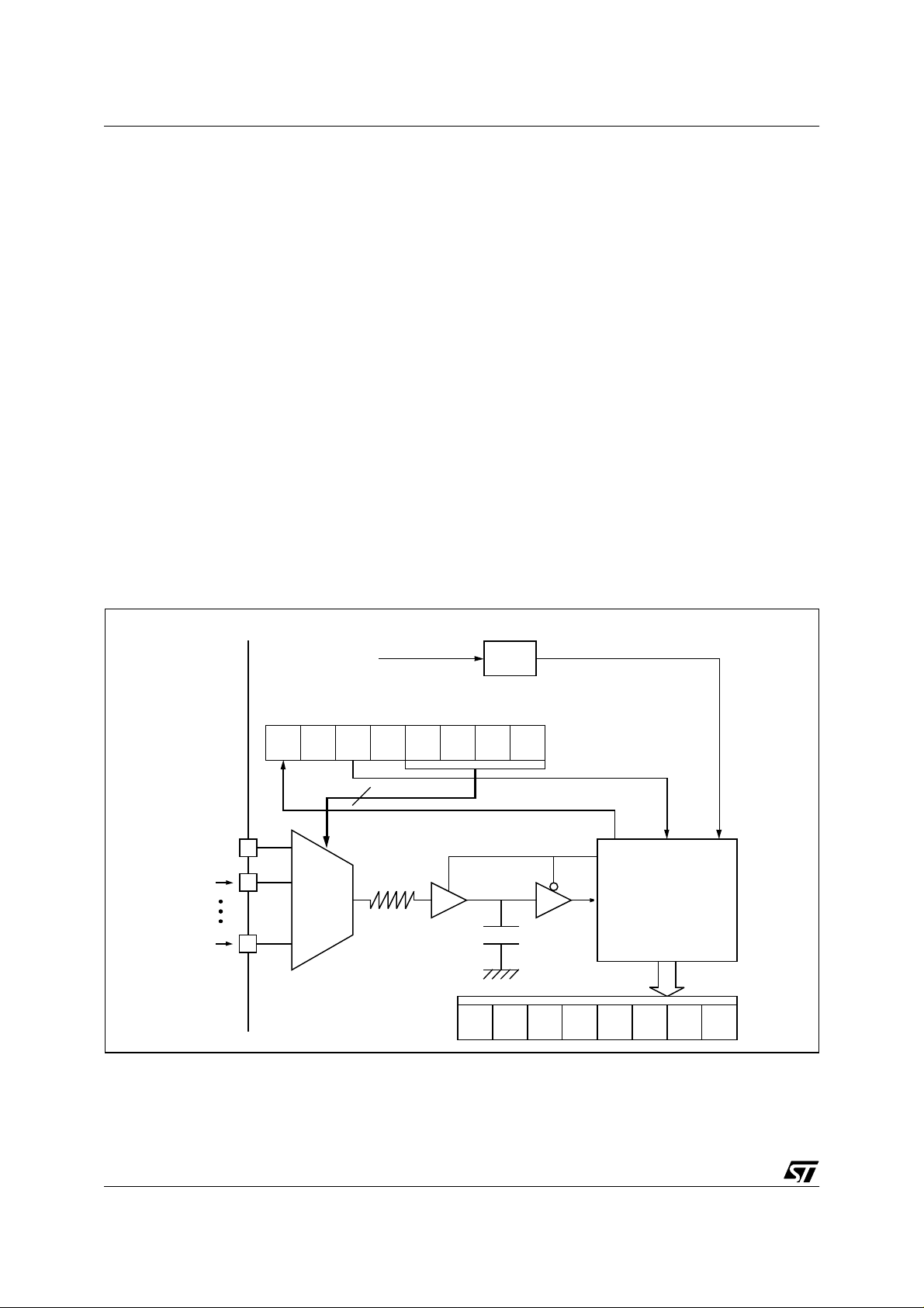
ST7263B
11.6 8-BIT A/D CONVERTER (ADC)
11.6.1 Introduction
The on-chip Analog to Digital Converter ( ADC) peripheral is a 8-bit, successive approximation converter with internal sample and hold circuitry. This
peripheral has up to 16 m ultiplexed analog input
channels (refer to device pin out description) that
allow the peripheral to convert the analog vol tage
levels from up to 16 different sources.
The result of the conversion is stored in a 8-bit
Data Register. The A/D converter is controlled
through a Control/Status Register.
11.6.2 Main Features
■ 8-bit conversion
■ Up to 16 channels with multiplexed input
■ Linear successive approximation
■ Data register (DR) which contains the results
■ Conversion complete status flag
■ On/off bit (to reduce consumption)
The block diagram is shown in Figure 43.
Figure 43. ADC Block Diagram
f
CPU
11.6.3 Functional Description
11.6.3.1 Analog Power Supply
V
DDA
and V
are the high and low level refer-
SSA
ence voltage pins. In some devices (refer to device
pin out description) they are internally connected
to the V
and VSS pins.
DD
Conversion accuracy may therefore be impacted
by voltage drops a nd no ise in th e ev ent of heavily
loaded or badly decoupled power supply lines.
See electrical characteristics section for m ore details.
f
DIV 4
ADC
86/132
AIN0
AIN1
AINx
ANALOG
MUX
4
R
ADC
ADCDR
CH2 CH1CH3COCO 0 ADON 0 CH0
HOLD CONTROL
C
ADCCSR
ADC
ANALOG TO DIGITAL
CONVERTER
D2
D1D3D7 D6 D5 D4 D0
Page 87
8-BIT A/D CONVERTER (ADC) (Cont’d)
11.6.3.2 Digital A/D Conversion Result
The conversion is monotonic, meaning that the result never decreases if t he analog i nput does not
and never increases if the analog input does not.
If the input voltage (V
to V
(high-level voltage reference) then the
DDA
) is greater than or equal
AIN
conversion result in the DR register is FFh (full
scale) without overflow indication.
If input voltage (V
V
(low-level voltage reference) then the con-
SSA
) is lower than or equal to
AIN
version result in the DR register is 00h.
The A/D converter is linear and the digital result of
the conversion is stored in the ADCDR register.
The accuracy of the conversion is described in the
parametric section.
is the maximum recommended impedance
R
AIN
for an analog input signal. If the impedance is too
high, this will result in a loss of accur acy due to
leakage and sampling not being completed in the
alloted time.
11.6.3.3 A/D Conversion Phases
The A/D conversion is based on two conversion
phases as shown in Figure 44:
■ Sample capacitor loading [duration: t
During this phase, the V
measured is loaded into the C
input voltage to b e
AIN
ADC
]
LOAD
sample
capacitor.
■ A/D conversion [duration: t
CONV
]
During this phase, the A/D conversion is
computed (8 successive approximat ions cycles)
and the C
sample capacitor is disconnected
ADC
from the analog input pin to get the optimum
analog to digital conversion accuracy.
While the ADC is on, these two phases are continuously repeated.
At the end of each conversion, the sample capacitor is kept loaded with the pr evious measurem ent
load. The advantage of this behaviour is that it
minimizes the curre nt consum ption on the analog
pin in case of single input channel measurement.
11.6.3.4 Software Procedure
Refer to the control/status register (CSR) and data
register (DR) in Sectio n 11.6.6 for the bit defini-
tions and to Figure 44 for the timings.
ADC Configuration
The total duration of the A/D conversion is 12 ADC
clock periods (1/f
ADC
=4/f
CPU
).
ST7263B
The analog input ports must be configured as input, no pull-up, no interrupt. Refer to the «I/O
ports» chapter. Using thes e pins as analog inp uts
does not affect the ability of the port to b e read as
a logic input.
In the CSR register:
– Select the CH[3:0] bits to assign t he analog
channel to be converted.
ADC Conversion
In the CSR register:
– Set the ADON bit to enable the A/D converter
and to start the first conversion. From this time
on, the ADC performs a continuous conversion of the selected channel.
When a conversion is complete
– The COCO bit is set by hardware.
– No interrupt is generated.
– The result is in the DR register and remains
valid until the next conversion has ended.
A write to the CSR register (with ADON set) aborts
the current conversion, resets the COCO bit and
starts a new conversion.
Figure 44. ADC Conversion Timings
ADON
HOLD
CONTROL
t
LOAD
t
CONV
11.6.4 Low Power Modes
Mode Description
WAIT No effect on A/D Converter
A/D Converter disabled.
HALT
After wakeup from Halt mode, the A/D Converter requires a stabilisation time before accurate conversions can be performed.
Note: The A/D converter may be disabled by resetting the ADON bit. This feature allows reduced
power consumption when no conversion is needed
and between single shot conversions.
11.6.5 Interrupts
None
ADCCSR WRITE
OPERATION
COCO BIT SET
87/132
Page 88
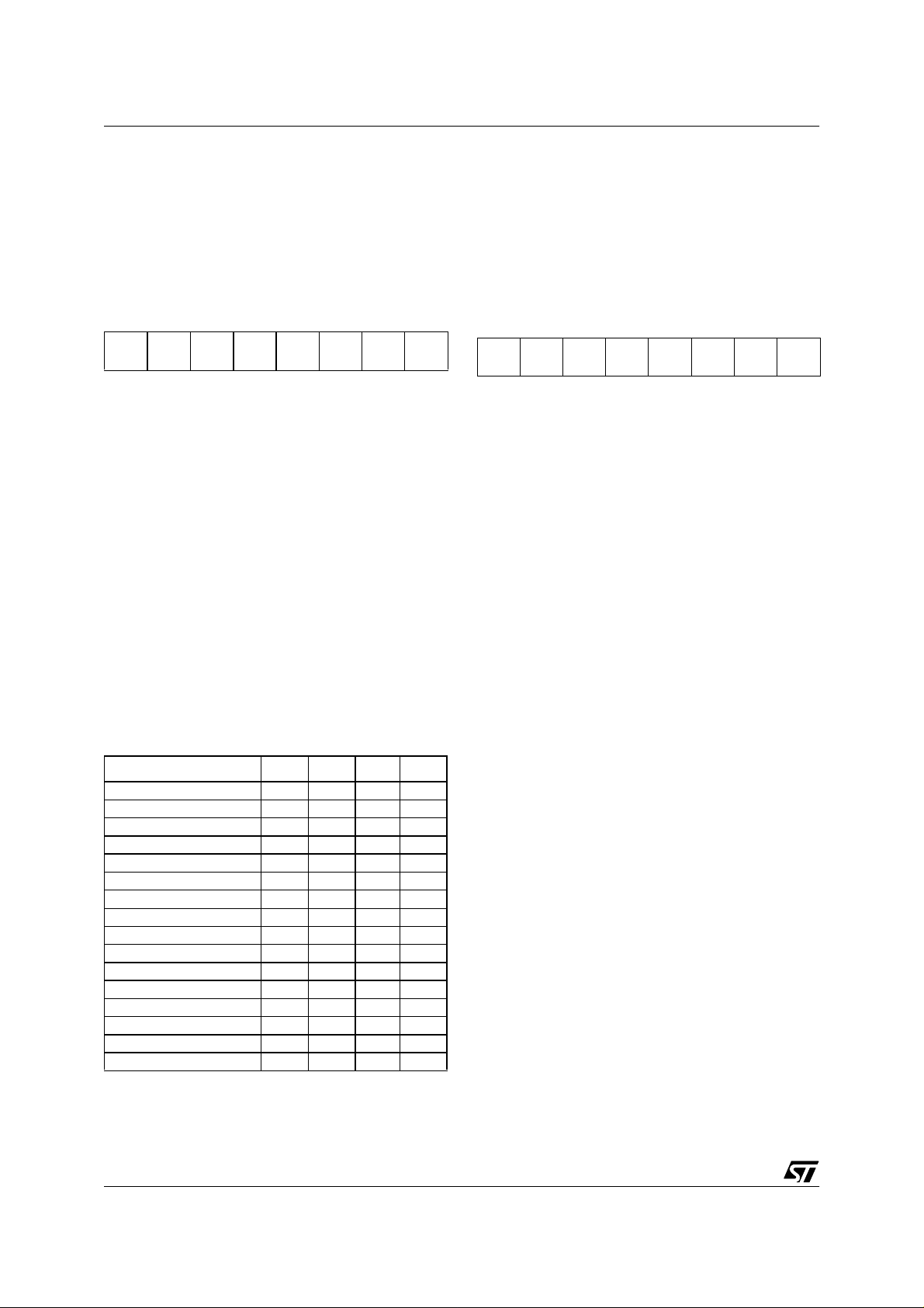
ST7263B
8-BIT A/D CONVERTER (ADC) (Cont’d)
11.6.6 Register Description
CONTROL/STATUS REGISTER (CSR)
Read/Write
Reset Value: 0000 0000 (00h)
70
COCO 0 ADON 0 CH3 CH2 CH1 CH0
Bit 7 = COCO
Conversion Complete
This bit is set by hardware. It is cleared by software reading the result in the DR register or writing
to the CSR register.
0: Conversion is not complete
1: Conversion can be read from the DR register
Bit 6 = R eserved .
Bit 5 = ADON
must always be cleared.
A/D Converter On
DATA REGISTER (DR)
Read Only
Reset Value: 0000 0000 (00h)
70
D7 D6 D5 D4 D3 D2 D1 D0
Bits 7:0 = D[7:0]
Analog Converted Value
This register contains the converted analog value
in the range 00h to FFh.
Note: Reading this register reset the COCO flag.
This bit is set and cleared by software.
0: A/D converter is switched off
1: A/D converter is switched on
Bit 4 = R eserved .
must always be cleared.
Bits 3:0 = CH[3:0]
Channel Selection
These bits are set and cleared by software. They
select the analog input to convert.
Channel Pin* CH3 CH2 CH1 CH0
AIN0 0 0 0 0
AIN1 0 0 0 1
AIN2 0 0 1 0
AIN3 0 0 1 1
AIN4 0 1 0 0
AIN5 0 1 0 1
AIN6 0 1 1 0
AIN7 0 1 1 1
AIN8 1 0 0 0
AIN9 1 0 0 1
AIN10 1 0 1 0
AIN11 1 0 1 1
AIN12 1 1 0 0
AIN13 1 1 0 1
AIN14 1 1 1 0
AIN15 1 1 1 1
*Note: The number of pins AND the channel selection varies according to the device. Refer to the device pinout.
88/132
Page 89

8-BIT A/D CONVERTER (ADC) (Cont’d)
Table 22. ADC Register Map
ST7263B
Address
(Hex.)
Register
Name
76543210
0Ah DR AD7 .. AD0
0Bh CSR CO CO 0 ADON 0 0 CH2 CH1 CH0
89/132
Page 90
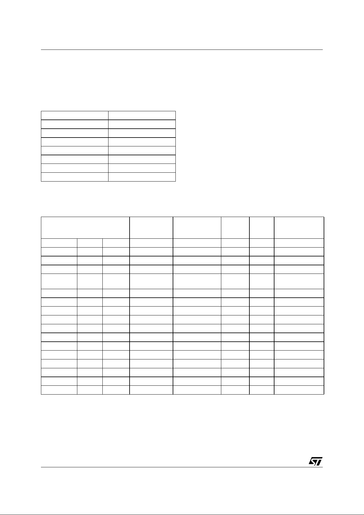
ST7263B
12 INSTRUCTIO N SET
12.1 ST7 ADDRESSING MODES
The ST7 Core features 17 different addressing
modes which can be classified in 7 main groups:
Addressing Mode Example
Inherent nop
Immediate ld A,#$55
Direct ld A,$55
Indexed ld A,($55,X)
Indirect ld A,([$55],X)
Relative jrne loop
Bit operation bset byte,#5
so, most of the ad dressing modes may be subdivided in two sub-modes called long and short:
– Long addressing mode is more powerful be-
cause it can use the full 64 Kbyte address space,
however it uses more bytes and more CPU cycles.
– Short addressing mode is less powerful because
it can generally only access page zero (0000h 00FFh range), but the instruction size is more
compact, and faster. All memory to memory instructions use short addressing modes only
(CLR, CPL, NEG, BSET, BRES, BTJT, BTJF,
INC, DEC, RLC, RRC, SLL, S RL, SRA, SWAP)
The ST7 Assembler optimizes the use of long and
short addressing modes.
The ST7 Instruction set is designed to minimize
the number of bytes required per instruction: To do
Table 23. ST7 Addressing Mode Overview
Mode Syntax
Inherent nop + 0
Immediate ld A,#$55 + 1
Short Direct ld A,$10 00..FF + 1
Long Direct ld A,$1000 0000..FFFF + 2
No Offset Direct Indexed ld A,(X) 00..FF
Short Direct Indexed ld A,($10,X) 00..1FE + 1
Long Direct Indexed ld A,($1000,X) 0000..FFFF + 2
Short Indirect ld A,[$10] 00..FF 00..FF byte + 2
Long Indirect ld A,[$10.w] 0000..FFFF 00..FF word + 2
Short Indirect Indexed ld A,([$10],X) 00..1FE 00..FF byte + 2
Long Indirect Indexed ld A,([$10.w],X) 0000..FFFF 00..FF word + 2
Relative D irect jrne loop PC-128/PC+127
Relative I ndire ct jrne [$10] PC-128 /PC+1 27
Bit Direct bset $10,#7 00..FF + 1
Bit Indirect bset [$10],#7 00..FF 00..FF byte + 2
Bit Direct Relative btjt $10,#7,skip 00..FF + 2
Bit Indirect Relative btjt [$10],#7,skip 00..FF 00..FF byte + 3
Destination/
Source
Pointer
Address
(Hex.)
1)
1)
00..FF byte + 2
Pointer
Size
(Hex.)
Length
(Bytes)
+ 0 (with X register)
+ 1 (with Y register)
+ 1
Note 1. At the time the instruction is executed, the Program Counter (PC) points to the instruction following JRxx.
90/132
Page 91
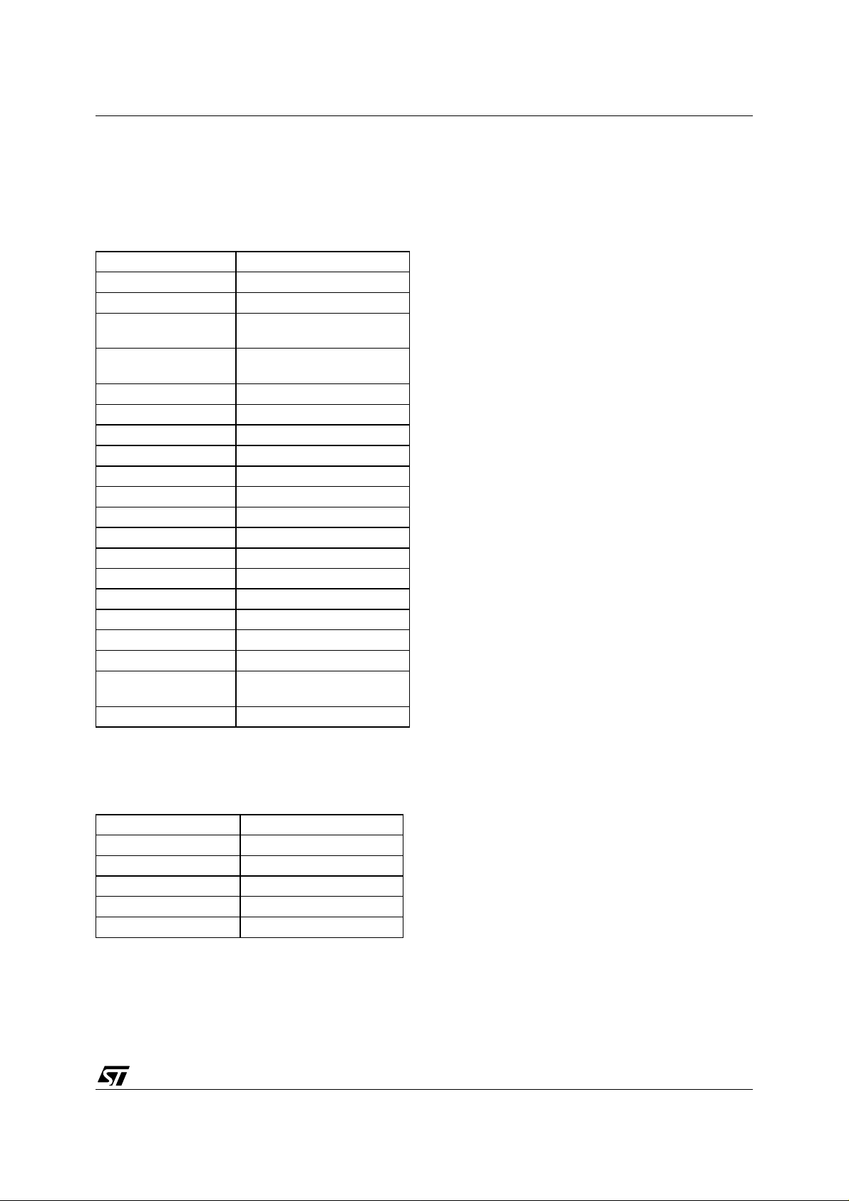
ST7 ADDRESSING MODES (Cont’d)
12.1.1 Inherent
All Inherent instructions consist of a single byte.
The opcode fully specifies all the required information for the CPU to process the operation.
Inherent Instruction Function
NOP No operation
TRAP S/W Interrupt
WFI
HALT
RET Sub-routine Return
IRET Interrupt Sub-routine Return
SIM Set Interrupt Mask
RIM Reset Interrupt Mask
SCF Set Carry Flag
RCF Reset Carry Flag
RSP Reset Stack Pointer
LD Load
CLR Clear
PUSH/POP Push/Pop to/from the stack
INC/DEC Increment/Decrement
TNZ Test Negative or Zero
CPL, NEG 1 or 2 Complement
MUL Byte Multiplication
SLL, SRL, SRA, RLC,
RRC
SWAP Swap Nibbles
Wait For Interrupt (Low Power
Mode)
Halt Oscillator (Lowest Power
Mode)
Shift and Rotate Operations
12.1.2 Immediate
Immediate instructions have two bytes, the first
byte contains the opcode, the second byte contains the operand value.
Immediate Instruction Function
LD Load
CP Compare
BCP Bit Compare
AND, OR, XOR Logical Operations
ADC, ADD, SUB, SBC Arithmetic Operations
ST7263B
12.1.3 Direct
In Direct instructions, the operands are referenced
by their memory address.
The direct addressing m ode consists of two submodes:
Direct (short)
The address is a byte, thus requires only one byte
after the opcode, but only allows 00 - FF addressing space.
Direct (lon g)
The address is a word, thus allowing 64 Kbyte addressing space, but requires 2 bytes after the opcode.
12.1.4 Indexed (No Offset, Short, Long)
In this mode, the operand is referenced by its
memory address, which is defined by the unsigned
addition of an index register (X or Y) with an offset.
The indirect addressing mode consists of three
sub-modes:
Indexed (No Offset)
There is no offset, (no extra byte after the opcode),
and allows 00 - FF addressing space.
Indexed (Short)
The offset is a byte, thus requires only one byte after the opcode and allows 00 - 1FE addressing
space.
Indexed (long)
The offset is a word, thus allowing 64 Kbyte addressing space and requires 2 byt es after the opcode.
12.1.5 Indirect (Short, Long)
The required data byte to do the operation is found
by its memory address, located in memory (pointer).
The pointer address follows th e op co de. Th e i ndirect addressing mode consists of two sub-modes:
Indirect (short)
The pointer address is a byte, the pointer size is a
byte, thus allowing 00 - FF addressing space, and
requires 1 byte after the opcode.
Indirect (lon g)
The pointer address is a byte, the pointer size is a
word, thus allowing 64 Kbyte addressing space,
and requires 1 byte after the opcode.
91/132
Page 92
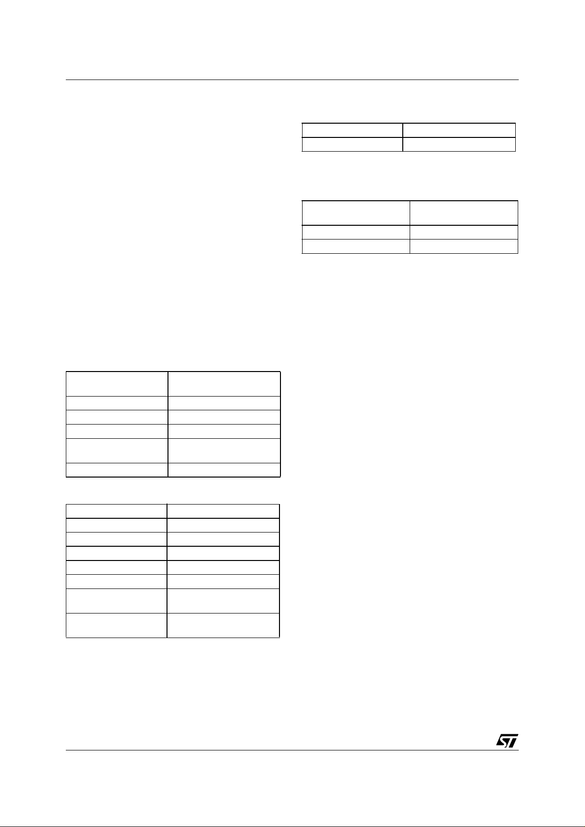
ST7263B
ST7 ADDRESSING MODES (Cont’d)
12.1.6 I ndi rect Indexed ( S hort, Long)
This is a combination of indirect and short indexed
addressing modes. The operand is referenced by
its memory address, which is defined by the unsigned addition of an index register value (X or Y)
with a pointer value located in memory. The pointer address follows the opcode.
The indirect indexed addressing mode consists of
two sub-modes:
Indirect Indexed (Short)
The pointer address is a byte, the pointer size is a
byte, thus allowing 00 - 1FE addressing space,
and requires 1 byte after the opcode.
Indirect Inde xed (Long)
The pointer address is a byte, the pointer size is a
word, thus allowing 64 Kbyte addressing space,
and requires 1 byte after the opcode.
Table 24. Instructions Supporting Direct,
Indexed, Indirect and Indirect Indexed
Addressing Modes
SWAP Swap Nibbles
CALL, JP Call or Jump subroutine
12.1.7 Relative Mode (Direct, Indirect)
This addressing mode is used to m odify the PC
register value by adding an 8-bit signed offset to it.
Available Relative Direct/
Indirect Instructions
JRxx Conditional Jump
CALLR Call Relative
Function
The relative addressing mode consists of two submodes:
Relative (Direct)
The offset follows the opcode.
Relative (Indirect)
The offset is defined in memory, of which t he address follows the opcode.
Long and Short
Instructions
LD Load
CP Compare
AND, OR, XOR Logical Operations
ADC, ADD, SUB, SBC
BCP Bit Compare
Short Instructions Only Function
CLR Clear
INC, DEC Increment/Decrement
TNZ Test Negative or Zero
CPL, NEG 1 or 2 Complement
BSET, BRES Bit Operations
BTJT, BTJF
SLL, SRL, SRA, RLC,
RRC
Arithmetic Addition/subtraction operations
Bit Test and Jump Operations
Shift and Rotate Operations
Function
92/132
Page 93
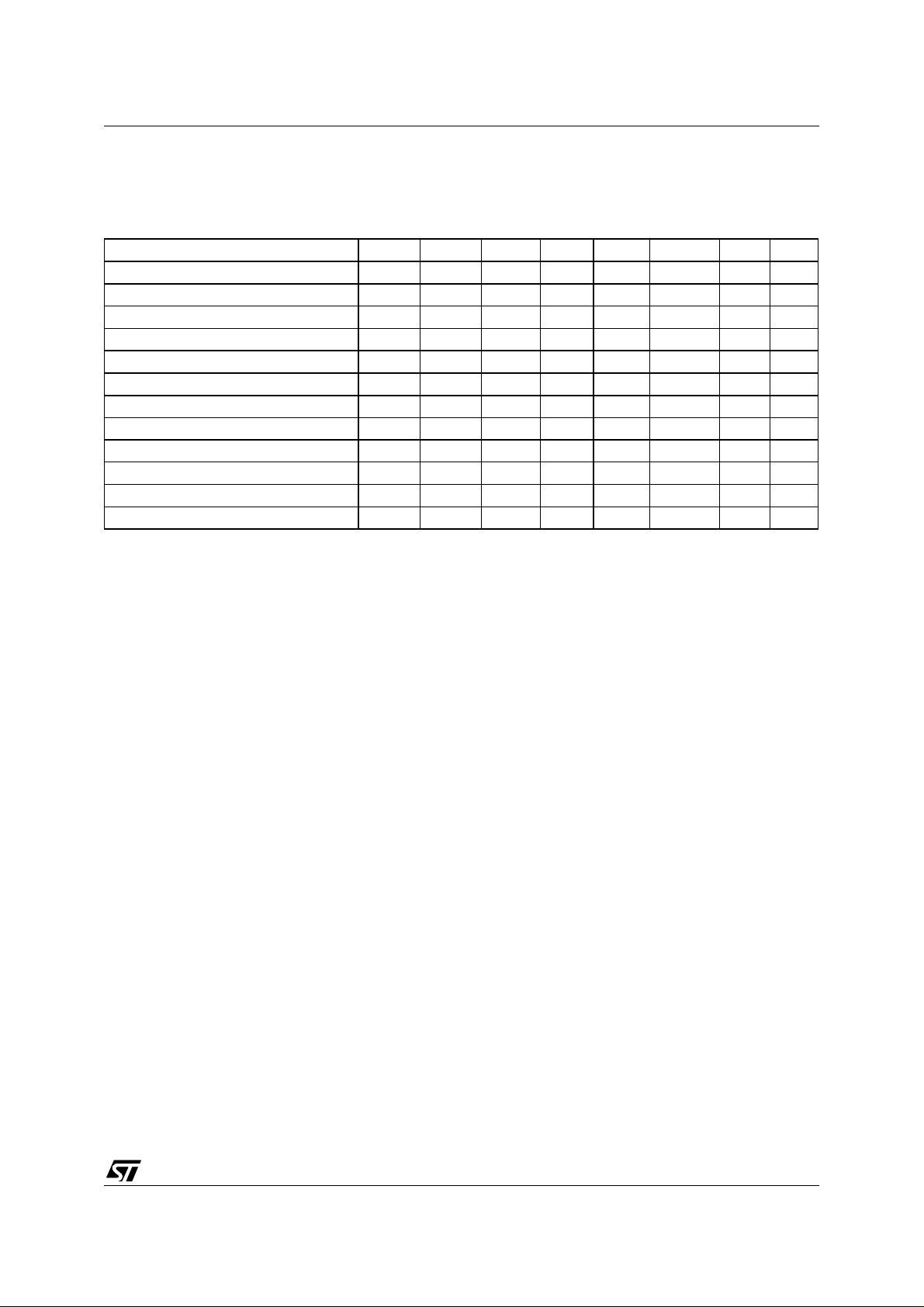
12.2 INSTRUCTION GROUPS
ST7263B
The ST7 family devices use an Instruction Set
consisting of 63 instructions. The instructions may
Load and Transfer LD CLR
Stack operation PUSH POP RSP
Increment/Decrement INC DEC
Compare and Tests CP TNZ BCP
Logical operations AND OR XOR CPL NEG
Bit Operation BSET BRES
Conditional Bit Test and Branch BTJT BTJF
Arithmetic operations ADC ADD SUB SBC MUL
Shift and Rotates SLL SRL SRA RLC RRC SWAP SLA
Unconditional Jump or Call JRA JRT JRF JP CALL CALLR NOP RET
Conditional Branch JRxx
Interruption management TRAP WFI HALT IRET
Condition Code Flag modification SIM RIM SCF RCF
be subdivided into 13 main groups as illustrated in
the following table:
Using a pre-b y te
The instructions are described with one to four
bytes.
In order to extend the number of available opcodes for an 8-bit CPU (256 opcodes), three different prebyte opcodes a re defined . These prebytes
modify the meaning of the instruction they precede.
The whole instruction becomes:
PC-2 End of previous instruction
PC-1 Prebyte
PC Opcode
PC+1 A dditional word (0 to 2) according to the
number of bytes required to compute the
effective address
These prebytes enable instruction in Y as well as
indirect addressing modes to be implemented.
They precede the opcode of the instruction in X or
the instruction using direct addres sing mode . The
prebytes are:
PDY 90 Replace an X based instruction using
immediate, direct, indexed, or inherent
addressing mode by a Y one.
PIX 92 Replace an instruction using direct, di-
rect bit, or direct relative addressing
mode to an instruction using the corresponding indirect addressing mode.
It also changes an instruction using X
indexed addressing mode to an instruction using indirect X indexed addressing
mode.
PIY 91 Replace an instruction using X indirect
indexed addressing mode by a Y one.
93/132
Page 94
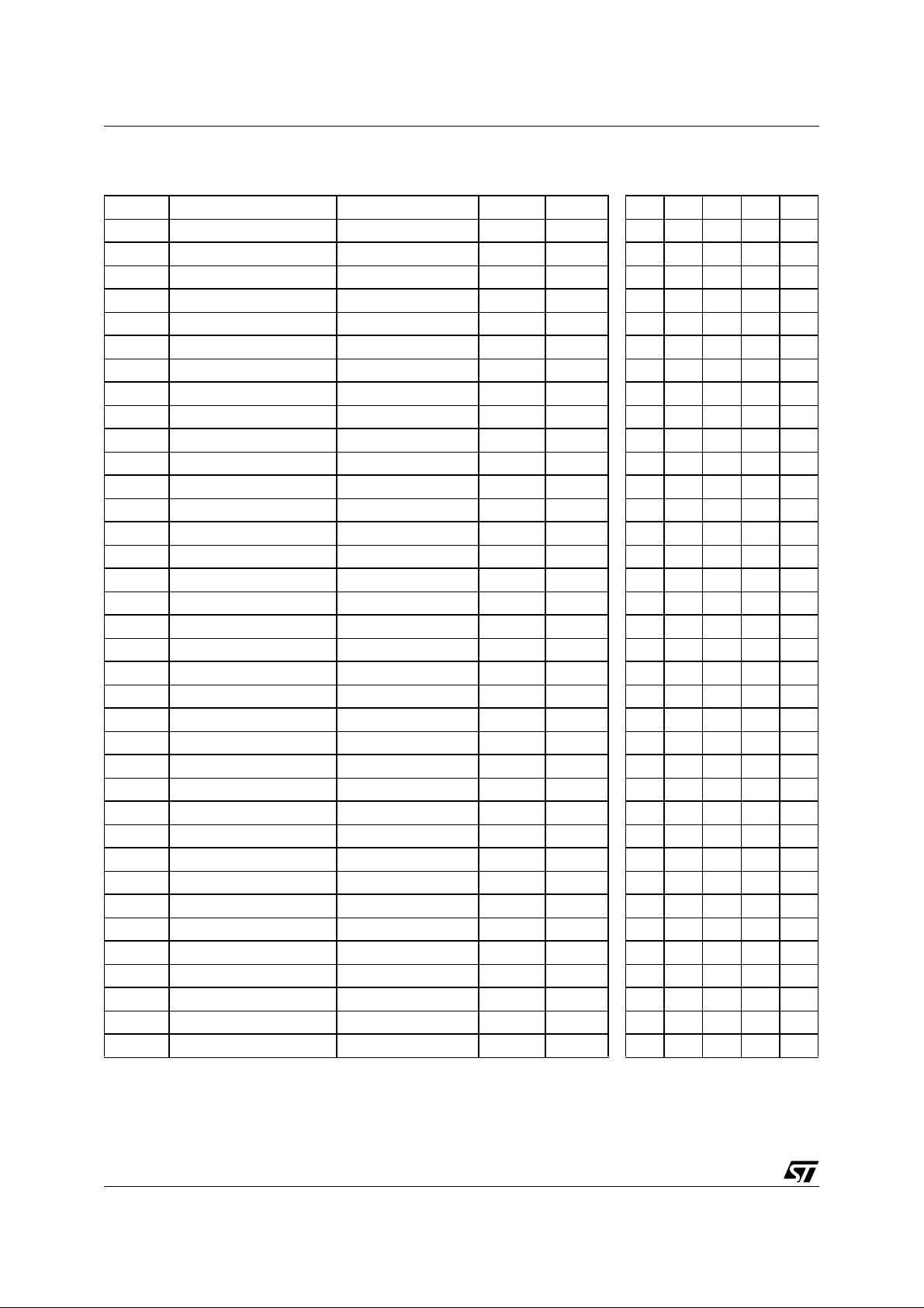
ST7263B
INSTRUCTION GROUPS (Cont’d)
Mnemo Description Function/Example Dst Src H I N Z C
ADC Add with Carry A = A + M + C A M H N Z C
ADD Addition A = A + M A M H N Z C
AND Logical And A = A . M A M N Z
BCP Bit compare A, Memory tst (A . M) A M N Z
BRES Bit Reset bres Byte, #3 M
BSET Bit Set bset Byte, #3 M
BTJF Jump if bit is false (0) btjf Byte, #3, Jmp1 M C
BTJT Jump if bit is true (1) btjt Byte, #3, Jmp1 M C
CALL Call subroutine
CALLR Call subroutine relative
CLR Clear reg, M 0 1
CP Arithmetic Compare tst(Reg - M) reg M N Z C
CPL One Complement A = FFH-A reg, M N Z 1
DEC Decrement dec Y reg, M N Z
HALT Halt 0
IRET Interrupt routine return Pop CC, A, X, PC H I N Z C
INC Increment inc X reg, M N Z
JP Abs olute Jump jp [TBL.w]
JRA Jump relative always
JRT Jump relative
JRF Never jump jrf *
JRIH Jump if ext. interrupt = 1
JRIL Jump if ext. interrupt = 0
JRH Jump if H = 1 H = 1 ?
JRNH Jump if H = 0 H = 0 ?
JRM Jump if I = 1 I = 1 ?
JRNM Jump if I = 0 I = 0 ?
JRMI Jump if N = 1 (minus) N = 1 ?
JRPL Jump if N = 0 (plus) N = 0 ?
JREQ Jump if Z = 1 (equal) Z = 1 ?
JRNE Jump if Z = 0 (not equal) Z = 0 ?
JRC Jump if C = 1 C = 1 ?
JRNC Jump if C = 0 C = 0 ?
JRULT Jump if C = 1 Unsigned <
JRUGE Jump if C = 0 Jmp if unsigned >=
JRUGT Jump if (C + Z = 0) Unsigned >
94/132
Page 95
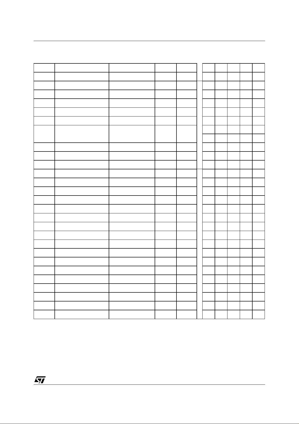
ST7263B
INSTRUCTION GROUPS (Cont’d)
Mnemo Description Function/Example Dst Src H I N Z C
JRULE Jump if (C + Z = 1) Unsigned <=
LD Load dst <= src reg, M M, reg N Z
MUL Multiply X,A = X * A A, X, Y X, Y, A 0 0
NEG Negate (2’s compl) neg $10 reg, M N Z C
NOP No Operation
OR OR operation A = A + M A M N Z
POP Pop from the Stack pop reg reg M
pop CC CC M H I N Z C
PUSH Push onto the Stack push Y M reg, CC
RCF Reset carry flag C = 0 0
RET Subroutine Return
RIM Enable Interrupts I = 0 0
RLC Rotate left true C C <= Dst <= C reg, M N Z C
RRC Rotate right true C C => Dst => C reg, M N Z C
RSP Reset Stack Pointer S = Max allowed
SBC Subtract with Carry A = A - M - C A M N Z C
SCF Set carry flag C = 1 1
SIM Disable Interrupts I = 1 1
SLA Shift left Arithmetic C <= Dst <= 0 reg, M N Z C
SLL Shift left Logic C <= Dst <= 0 reg, M N Z C
SRL Shift right Logic 0 => Dst => C reg, M 0 Z C
SRA Shift right Arithmetic Dst7 => Dst => C reg, M N Z C
SUB Subtraction A = A - M A M N Z C
SWAP SWAP nibbles Dst[7..4] <=> Dst[3..0] reg, M N Z
TNZ Test for Neg & Zero tnz lbl1 N Z
TRAP S/W trap S/W interrupt 1
WFI Wait for Interrupt 0
XOR Exclusive OR A = A XOR M A M N Z
95/132
Page 96
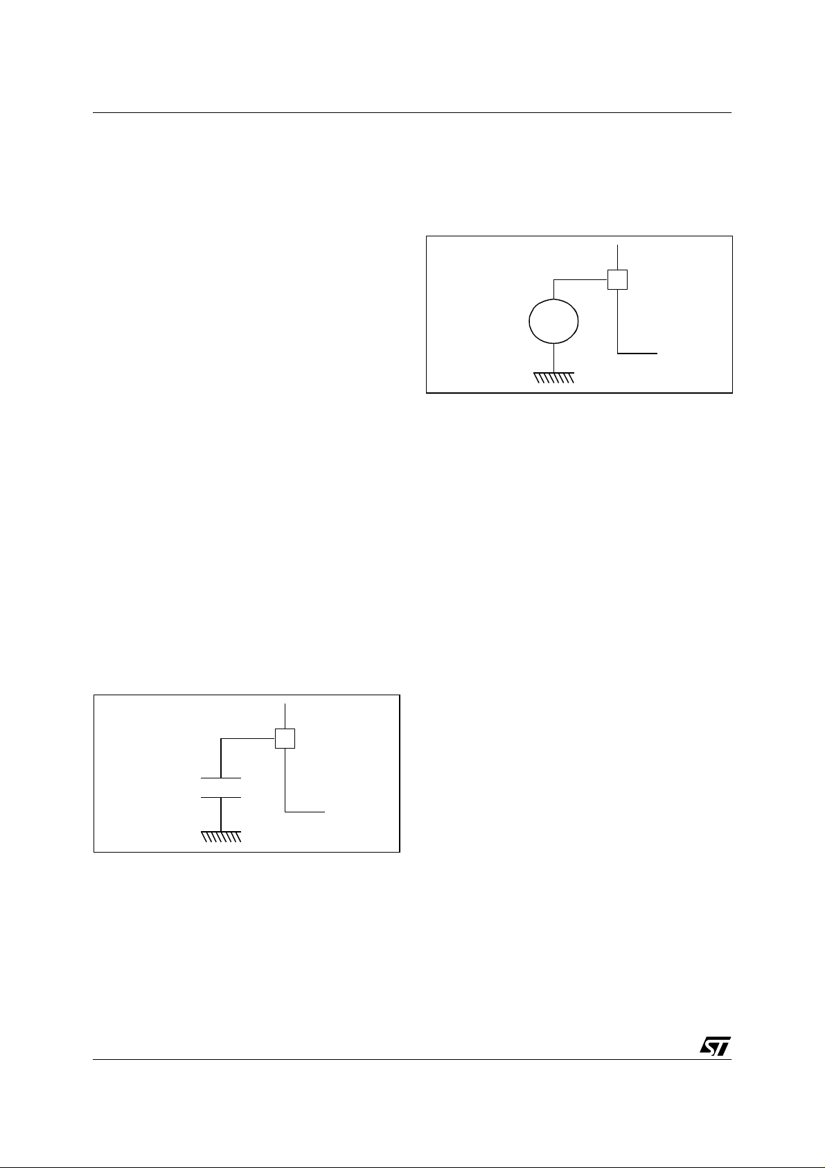
ST7263B
13 ELECTRIC AL CHARACTERISTICS
13.1 PARAMETER CONDITIONS
Unless otherwise specified, all voltages are referred to V
SS
.
13.1.1 Minimum and Maximum values
Unless otherwise specified the minimum and maximum values are guaranteed in the worst conditions of ambient t emperature, supp ly voltage an d
frequencies by tests in production on 100% of the
devices with an ambient temp erature at T
and T
max (given by the selected temperature
A=TA
=25°C
A
range).
Data based on characterization results, design
simulation and/or technology characteristics are
indicated in the table foo tnotes and are not teste d
in production. Based on characterization, the mi nimum and maximum values refer to sample tests
and represent the mean value plus or minus three
times the standard deviation (mean±3Σ).
13.1.2 Typical values
Unless otherwise specified, typical data are based
on T
=25°C, VDD=5V. They are given only as de-
A
sign guidelines and are not tested.
13.1.3 Typical curves
Unless otherwise specified, all typical curves are
given only as design guidelines and are not tested.
13.1.4 Loading capacitor
The loading conditions used for pin parameter
measurement are shown in Figure 45.
Figure 46. Pin input voltage
V
IN
ST7 PIN
Figure 45. Pin loading conditions
ST7 PIN
C
L
13.1.5 Pin input voltage
The input voltage measurement on a pin of the device is described in Figure 46.
96/132
Page 97
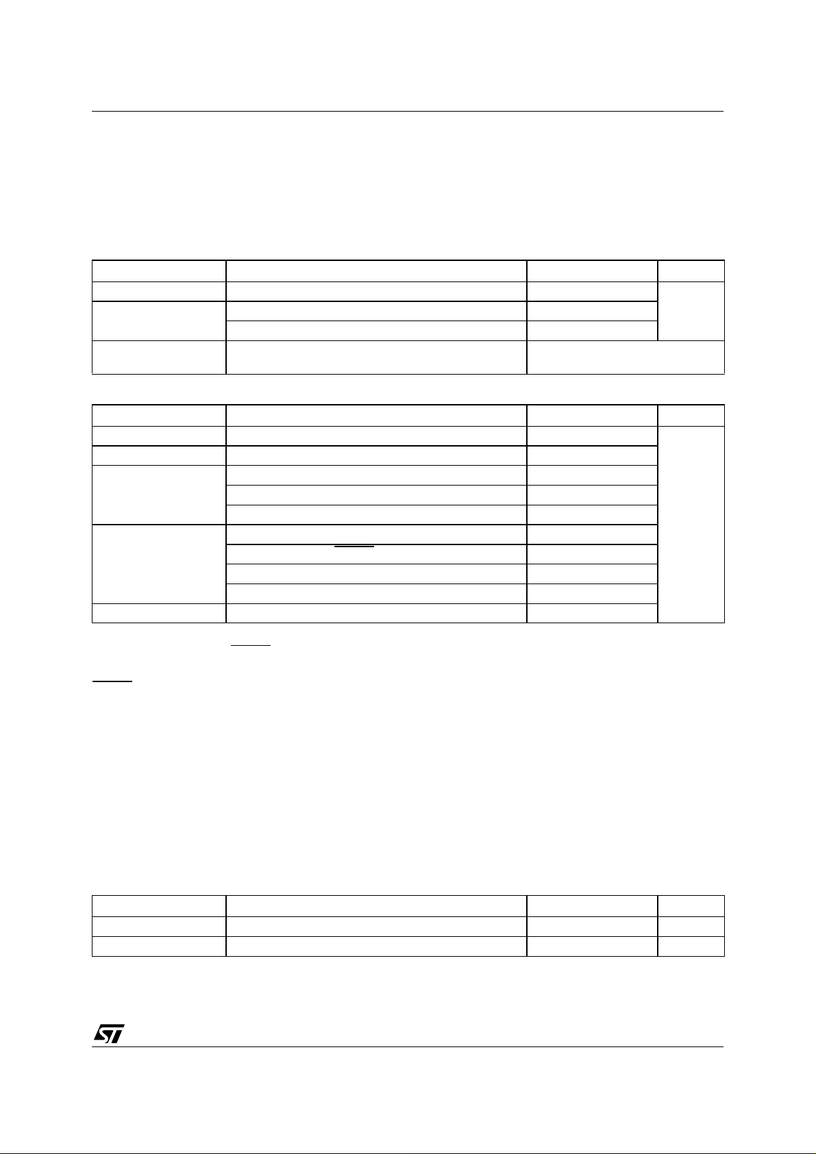
13.2 ABSOLUTE MAXIMUM RATINGS
ST7263B
Stresses above those listed as “absolute maximum ratings” may cause permanent damage to
the device. This is a stress rating only and func -
tions is not implied. Exposure to maximum rating
conditions for extended periods may affect device
reliabili ty.
tional operation of the device under these cond i-
13.2.1 Voltage Characteristics
Symbol Ratings Maximum value Unit
V
- V
DD
1) & 2)
V
IN
V
ESD(HBM)
SS
Supply voltage 6.0
Input voltage on true open drain pins VSS-0.3 to 6.0
Input voltage on any other pin V
Electro-static discharge voltage (Human Body Model)
-0.3 to VDD+0.3
SS
See “Absolute Electrical Sensitivity”
on page 105.
V
13.2.2 Current Characteristics
Symbol Ratings Maximum value Unit
I
VDD
I
VSS
Total current into VDD power lines (source)
Total current out of VSS ground lines (sink)
3)
3)
80
80
Output current sunk by any standard I/O and control pin 25
Output current sunk by any high sink I/O pin 50
Output current source by any I/Os and control pin - 25
Injected current on VPP pin TBD
Injected current on RESET
pin ± 5
Injected current on OSCIN and OSCOUT pins ± 5
Injected current on any other pin
5) & 6)
Total injected current (sum of all I/O and control pins)
5)
TBD
± 20
mA
I
INJ(PIN)
I
Σ
INJ(PIN)
I
IO
2) & 4)
2)
Notes:
1. Directly connectin g the RES ET
and I/O pins to VDD or V
is generated or an unexpected change of the I/O configuration occurs (for example, due to a corrupted program counter).
could damage the dev ice if an uni ntenti onal int ernal re set
SS
To guarantee safe operation, th is connectio n has to be don e through a pull-up or pull-down r esistor (typic al: 4.7kΩ for
RESET
, 10kΩ for I/Os). Unused I/O pins must be tied in the same way to VDD or VSS according to their reset configuration.
2. When the current limitation is not possible , the V
specification. A positive injection is induced by VIN>VDD while a negative injection is induced by VIN<VSS.
I
INJ(PIN)
3. All power (V
) and ground (VSS) lines must always be connected to the external supply.
DD
absolute m aximum rating m ust be respected, otherwis e refer to
IN
4. Negative injection disturbs the analog performance of the device. In particular, it induces leakage currents throughout
the device including the analog inputs. To avoid undesirable effects on the analog functions, care must be taken:
- Analog input pins must have a negative injection less than 0.8 mA (assuming that the impedance of the analog voltage
is lower than the specified limits)
- Pure digital pins must have a negative injection less than 1.6mA. In addition, it is recommended to inject the current as
far as possible from the analog input pins.
5. When several inputs are submitted to a current injection , the maximum ΣI
and negative injected currents (instantaneous values). These results are based on characterisation with ΣI
mum current injection on four I/O port pins of the device.
is the absolute sum of the positive
INJ(PIN)
INJ(PIN)
maxi-
6. True open drain I/O port pins do not accept positive injection.
13.2.3 Thermal Characteristics
Symbol Ratings Value Unit
T
STG
T
J
Storage temperature range -65 to +150 °C
Maximum junction temperature TBD
97/132
Page 98
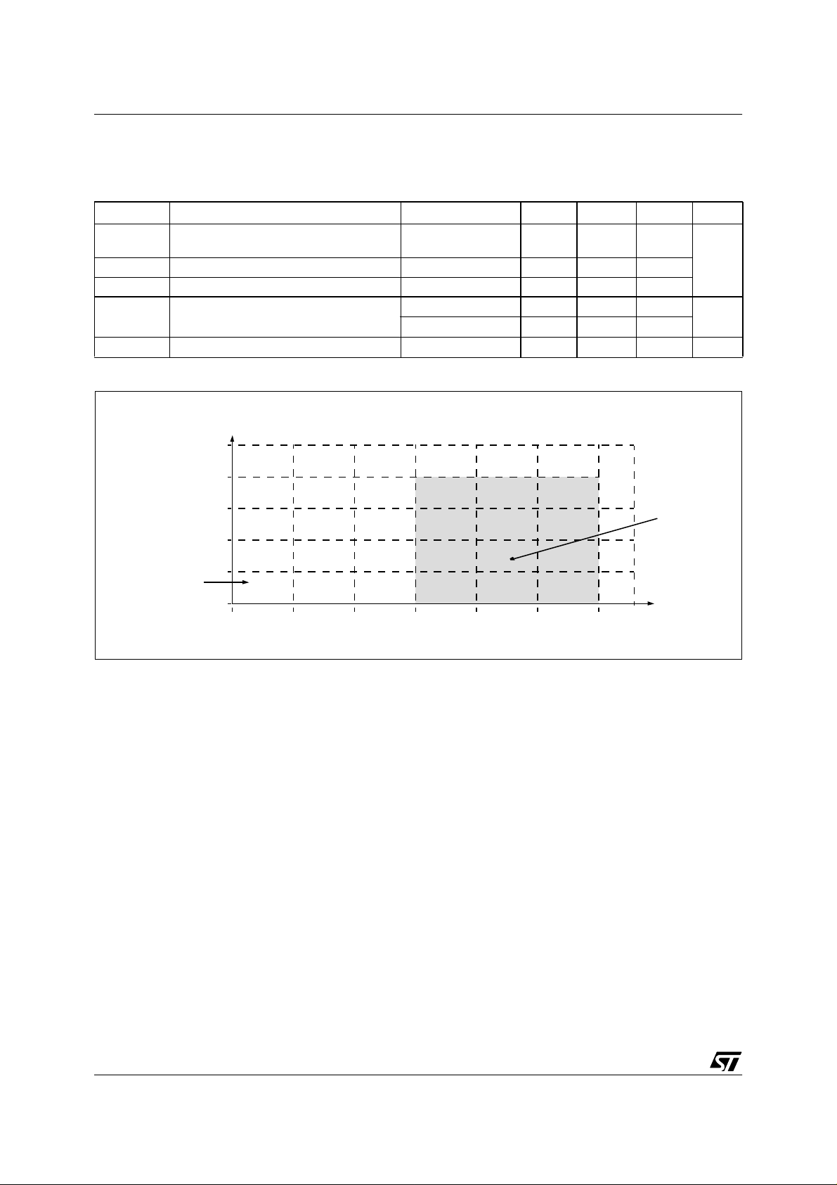
ST7263B
13.3 OPERATING CONDITIONS
13.3.1 General Operating Condi tions
Symbol Parameter Conditions Min Typ Max U nit
Operating Supply Voltage
(No USB)
f
= 8 MHz 4 5 5.5
CPU
Analog reference voltage V
Analog reference voltage V
f
= 24 MHz 8
Operating frequency
OSC
f
= 12 MHz 4
OSC
Ambient temperatur e range
DD
SS
V
DD
V
SS
070°C
V
V
V
f
CPU
DD
DDA
SSA
T
A
V
MHz
Figure 47. f
FUNCTIONALITY
NOT GUARANTEED
CPU
IN THIS AREA
Maximum Operating Frequency Versus V
f
[MHz]
CPU
8
4
2
0
2.5 3.0 3.5 4 4.5 5 5.5
Supply Volta ge
DD
FUNCTIONALITY
GUARANTEED
FROM 4 TO 5.5 V
SUPPLY VOLTAGE [V]
98/132
Page 99

OPERATING CONDITIONS (Cont’d)
13.3.2 Operating Conditions with Low Voltage Detector (LVD)
, f
Subject to general operating conditions for V
DD
Symbol Parameter Conditions Min Typ
V
V
V
Vt
IT+
IThyst
POR
Low Voltage Reset Threshold (VDD rising) VDD Max. Variation 50V/ms 3.6 3.7 3.8 V
Low Voltage Reset Threshold (VDD falling) VDD Max. Variation 50V/ms 3.3 3.5 3.7 V
Hysteresis (V
VDD rise time rate
IT+
- V
) 180 200 220 mV
IT-
2)
Notes:
1. Not tested, guaranteed by design.
2. The V
rise time rate condition is needed to insure a correct device power-on and LVD reset. Not tested in production.
DD
, and TA. Refer to Figure 9 on page 17.
CPU
0.5 50 V/ms
1)
ST7263B
Max Unit
99/132
Page 100
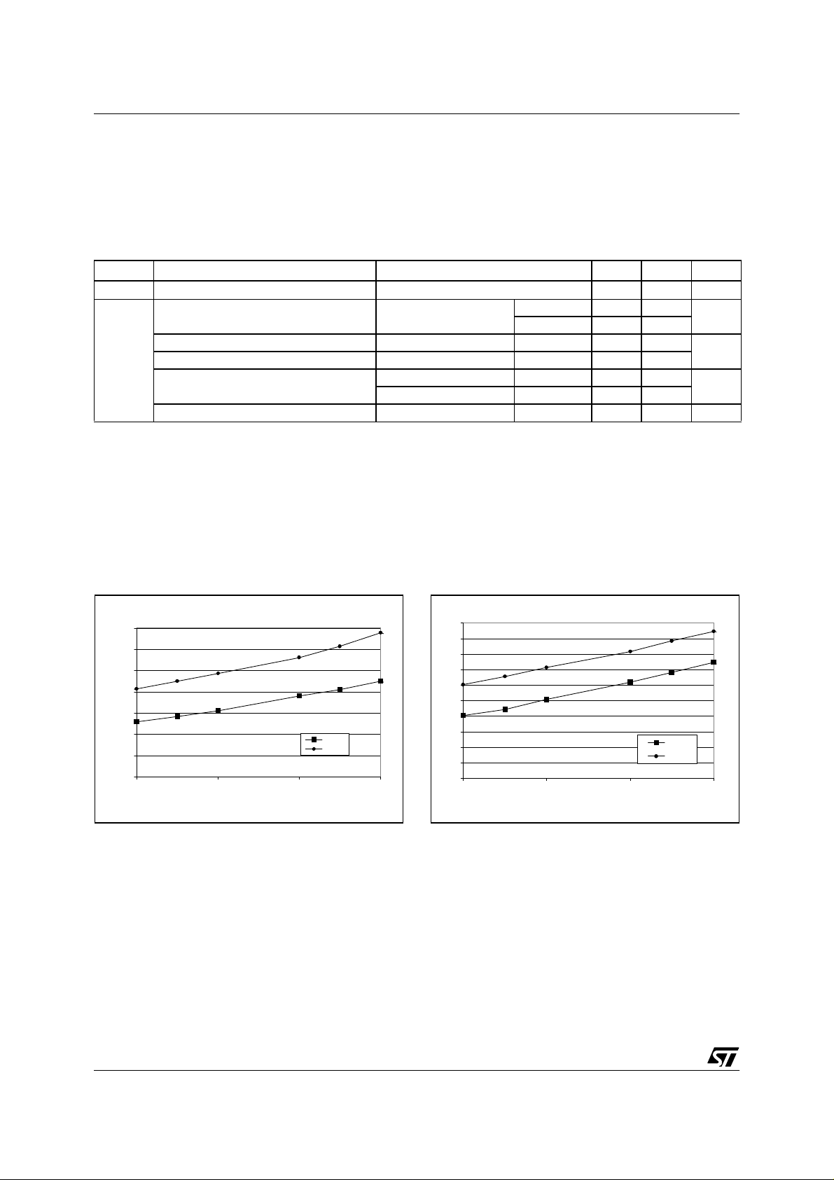
ST7263B
13.4 SUPPLY CURRENT CHARACTERISTICS
The following current consumption specified for
the ST7 functional operating modes over tempera-
added (except for HALT m ode for which the clock
is stopped).
ture range does not take into account the clock
source current consumption. To get the total device consumption, the two current values must be
Symbol Parameter Conditions Typ
I
∆
DD(∆Ta)
I
Note 1: Typical data are based on TA=25°C and not tested in production
Note 2: Oscillator and watchdog running.
Note 3: USB Transceiver and ADC are powered down.
Note 4: Low voltage reset function enabled.
Figure 48. Typ. IDD in RUN at 4 and 8 MHz f
Supply current variation vs. temperature Constant VDD and f
CPU RUN mode I/Os in input mode
CPU WAIT mode f
DD
CPU HALT mode
USB Suspend mode
4)
with LVD 120 150
without LVD 20 30
CPU
= 4 MHz 7.5 9
f
CPU
f
= 8 MHz 12 13.5
CPU
= 4 MHz 6 7.5
CPU
f
= 8 MHz 8.5 9.5
CPU
All others peripherals disabled.
CPU in HALT mode.
Current consumption of external pull-up (1.5Kohms to USBVCC) and pull-down (15Kohms to V
not included.
CPU
Figure 49. Typ. IDD in WAIT at 4 and 8 MHz f
1)
Max Unit
10 %
2)
120 150
SSA
mA
2)
mA
2)
3)
3)
A
µ
A
µ
)
CPU
14
12
10
8
6
Idd run ( mA )
4
2
0
44.555.5
Vdd (V )
4 mHz
8 mHz
10
9
8
7
6
5
4
Idd wait (mA)
3
2
1
0
44.5 55.5
Vdd (V)
4 mHz
8 mHz
100/132
 Loading...