

Page 1
查询ST16C554DCJ68 供应商
DESCRIPTION
ST16C554/554D
ST68C554
QUAD UART WITH 16-BYTE FIFOS
The ST16C554D is a universal asynchronous receiver
and transmitter (UART) with a dual foot print interface.
The 554D is an enhanced UART with 16 byte FIFOs,
receive trigger levels and data rates up to 1.5Mbps.
Onboard status registers provide the user with error
indications and operational status, modem interface
control. System interrupts may be tailored to meet
user requirements. An internal loopback capability
allows onboard diagnostics. The 554D is available in
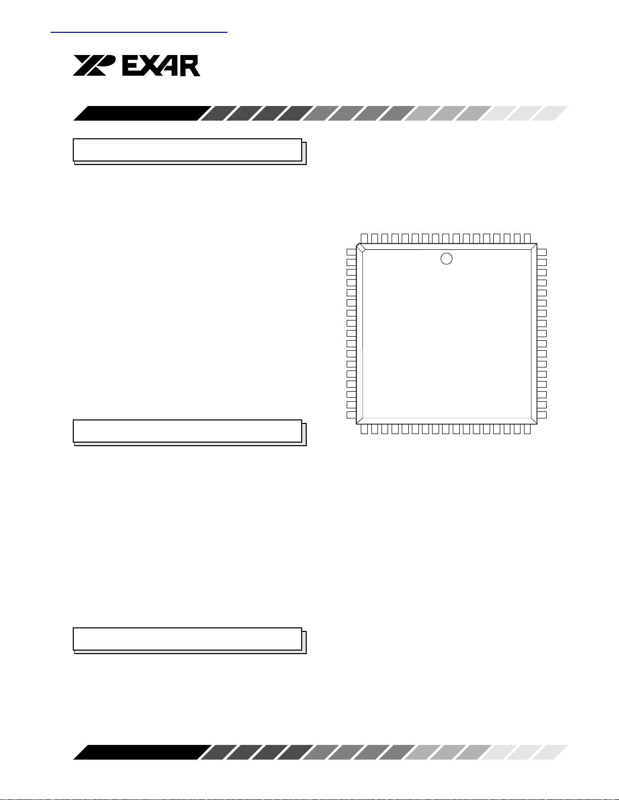
64 pin TQFP, and 68 pin PLCC packages. The 68 pin
PLCC package offer an additional 68 mode which
allows easy integration with Motorola, and other popu-
lar microprocessors. The ST16C554CQ64 (64 pin)
offers three state interrupt control while the
ST16C554DCQ64 provides constant active interrupt
outputs. The 64 pin devices do not offer TXRDY/
RXRDY outputs. The 554D combines the package
interface modes of the 16C554 and 68C554 series on
a single integrated chip.
FEATURES
• Compatibility with the Industry Standard
ST16C454, ST68C454, ST68C554, TL16C554
• 1.5 Mbps transmit/receive operation (24MHz)
• 16 byte transmit FIFO
• 16 byte receive FIFO with error flags
• Independent transmit and receive control
• Software selectable Baud Rate Generator
• Four selectable Receive FIFO interrupt trigger
levels
• Standard modem interface
-DSRA
-CTSA
-DTRA
VCC
-RTSA
INTA
-CSA
TXA
-IOW
TXB
-CSB
INTB
-RTSB
GND
-DTRB
-CTSB
-DSRB
PLCC Package
-CDA
-RIA
RXA
987654321
10
11
12
13
14
15
16
17
18
19
20
21
22
23
24
25
26
2728293031323334353637383940414243
-CDB
GNDD7D6D5D4D3D2D1D0
ST16C554DCJ68
16 MODE
-RIB
RXB
A2A1A0
VCC
16/-68
68676665646362
XTAL1
XTAL2
INTSEL
RESET
-TXRDY
-RXRDY
VCC
GND
RXD
-RID
-CDD
61
60
-DSRD
59
-CTSD
-DTRD
58
GND
57
-RTSD
56
55
INTD
54
-CSD
TXD
53
-IOR
52
TXC
51
-CSC
50
49
INTC
-RTSC
48
VCC
47
-DTRC
46
45
-CTSC
44
-DSRC
-RIC
RXC
-CDC
ORDERING INFORMATION
Part number Pins Package Operating temperature
ST16C554DCJ68 68 PLCC 0° C to + 70° C
ST16C554DCQ64 64 TQFP 0° C to + 70° C
ST16C554CQ64 64 TQFP 0° C to + 70° C
ST16C554DIJ68 68 PLCC -40° C to + 85° C
ST16C554DIQ64 64 TQFP -40° C to + 85° C
Rev. 3.10
EXAR Corporation, 48720 Kato Road, Fremont, CA 94538 • (510) 668-7000 • FAX (510) 668-7017
Page 2
ST16C554/554D/68C554
D
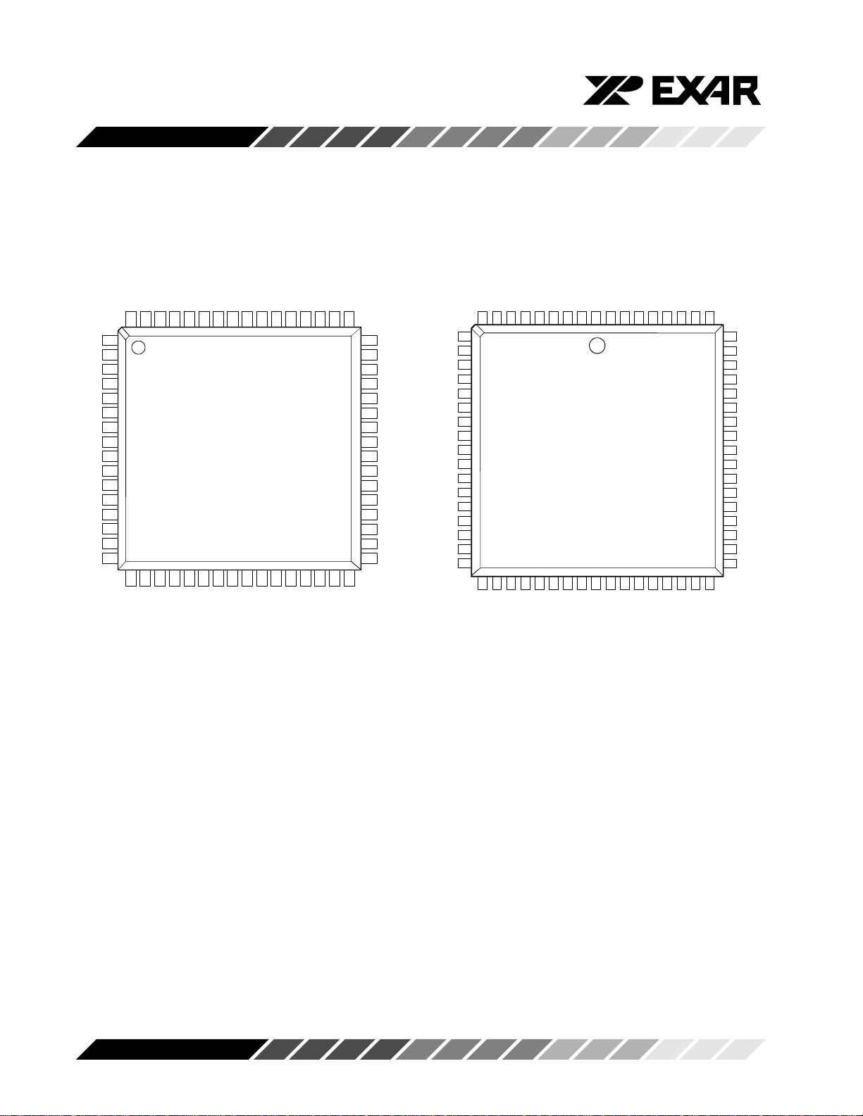
Figure 1, Package Descriptions
64 Pin TQFP Package 68 Pin PLCC Package
-CDA
-RIA
RXA
-DSRA
-CTSA
-DTRA
VCC
-RTSA
INTA
-CSA
TXA
-IOW
-TXB
-CSB
INTB
-RTSB
GND
-DTRB
-CTSB
GNDD7D6D5D4D3D2D1D0
646362616059585756555453525150
1
2
3
4
5
6
7
8
9
10
11
12
13
14
15
16
171819202122232425262728293031
-CDB
-DSRB
ST16C554CQ64
ST16C554DCQ64
RXB
VCC
A2A1A0
-RIB
XTAL1
XTAL2
VCC
RXD
-RID
-CDD
49
-DSRD
48
-CTSD
47
-DTRD
46
GND
45
-RTSD
44
INTD
43
-CSD
42
TXD
41
-IOR
40
TXC
39
-CSC
38
INTC
37
-RTSC
36
VCC
35
-DTRC
34
-CTSC
33
32
-RIC
RXC
GND
RESET
-CDC
-DSRC
-DSRA
-CTSA
-DTRA
VCC
-RTSA
-IRQ
-CS
TXA
R/-W
TXB
A3
N.C.
-RTSB
GND
-DTRB
-CTSB
-DSRB
-CDA-RIA
RXA
987654321
10
11
12
13
14
15
16
17
18
19
20
21
22
23
24
25
26
2728293031323334353637383940414243
-CDB
GNDD7D6D5D4D3D2D1D0
ST16C554DCJ68
68 MODE
-RIB
RXB
A2A1A0
VCC
16/-68
68676665646362
XTAL1
XTAL2
N.C.
-RESET
-TXRDY
-RXRDY
VCC
GND
RXD
-RID
-CD
61
60
-DSRD
59
-CTSD
-DTRD
58
GND
57
-RTSD
56
55
N.C.
54
N.C.
TXD
53
N.C.
52
TXC
51
50
A4
49
N.C.
-RTSC
48
VCC
47
-DTRC
46
45
-CTSC
44
-DSRC
-RIC
RXC
-CDC
Rev. 3.10
2
Page 3
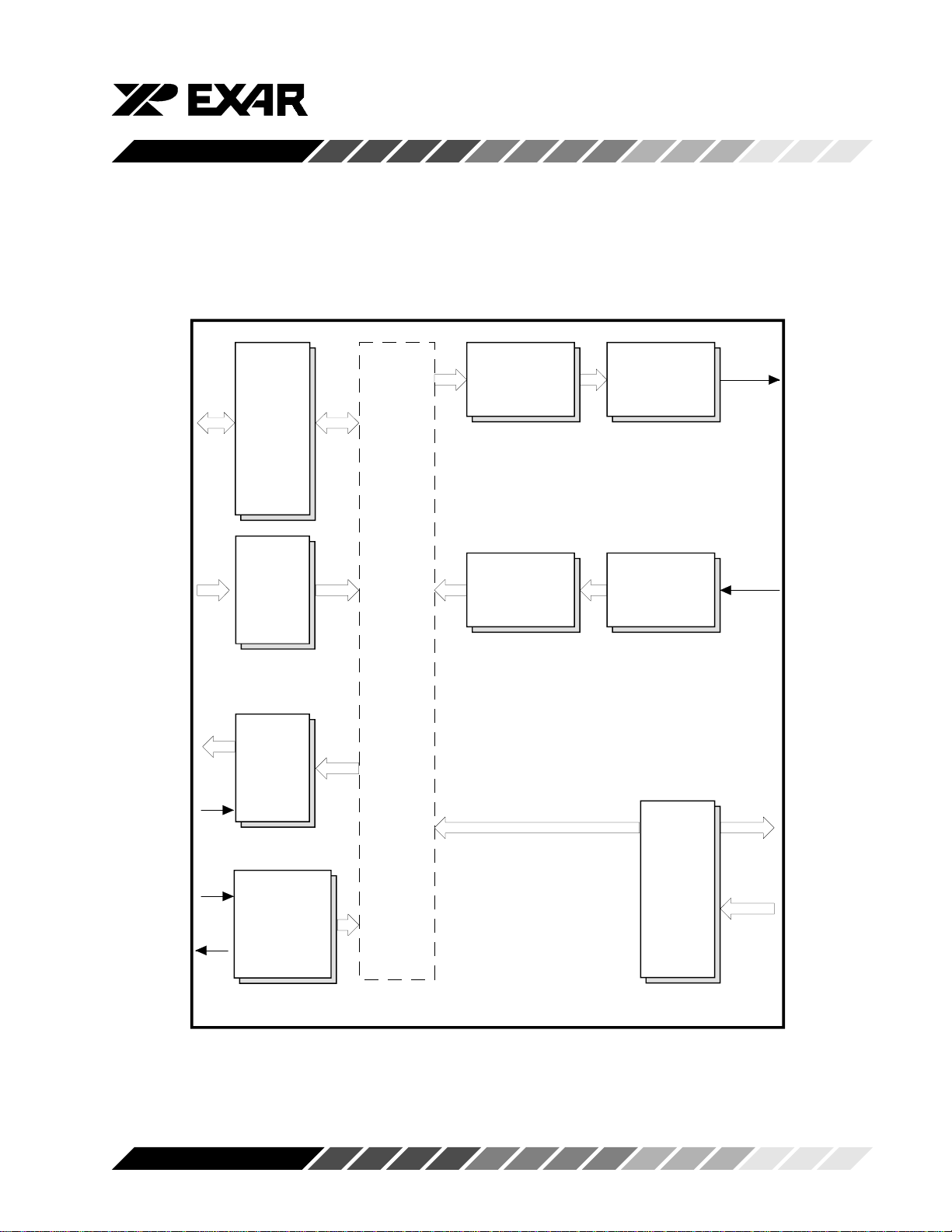
Figure 2, Block Diagram 16 Mode
I
ST16C554/554D/68C554
D0-D7
-IOR
-IOW
RESET
A0-A2
-CS A-D
NT A-D
-RXRDY
-TXRDY
INTSEL
Data bus
Register
Interrupt
&
Select
Control
Transmit
FIFO
Registers
Control Logic
Receive
Logic
&
Control signals
Inter Connect Bus Lines
Logic
FIFO
Registers
Transmit
Shift
Register
Receive
Shift
Register
TX A-D
RX A-D
-DTR A-D
-RTS A-D
Modem
XTAL1
&
XTAL2
Rev. 3.10
Clock
Generator
Baud Rate
3
Control
Logic
-CTS A-D
-RI A-D
-CD A-D
-DSR A-D
Page 4
ST16C554/554D/68C554
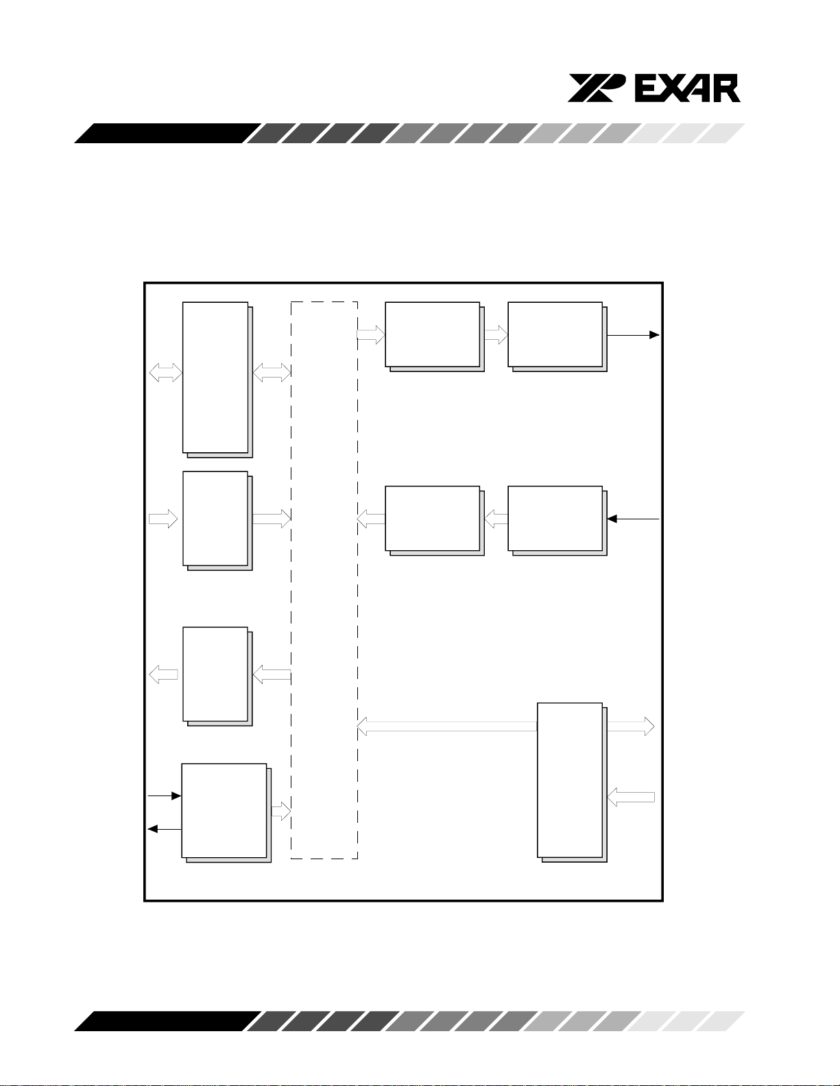
Figure 3, Block Diagram 68 Mode
D0-D7
R/-W
-RESET
A0-A4
-CS
-IRQ
-RXRDY
-TXRDY
Transmit
FIFO
Registers
&
Data bus
Control Logic
Receive
Logic
Select
Register
&
Control signals
Inter Connect Bus Lines
Logic
Control
Interrupt
FIFO
Registers
Transmit
Shift
Register
Receive
Shift
Register
TX A-D
RX A-D
-DTR A-D
-RTS A-D
XTAL1
XTAL2
Rev. 3.10
Modem
Control
&
Clock
Generator
Baud Rate
4
Logic
-CTS A-D
-RI A-D
-CD A-D
-DSR A-D
Page 5
ST16C554/554D/68C554
SYMBOL DESCRIPTION
Symbol Pin Signal Pin Description
68 64 type
16/-68 31 - I 16/68 Interface Type Select (input with internal pull-up). -
This input provides the 16 (Intel) or 68 (Motorola) bus
interface type select. The functions of -IOR, -IOW, INT A-
D, and -CS A-D are re-assigned with the logical state of this
pin. When this pin is a logic 1, the 16 mode interface
16C554D is selected. When this pin is a logic 0, the 68 mode
interface (68C554) is selected. When this pin is a logic 0, -
IOW is re-assigned to -R/W, RESET is re-assigned to -
RESET, -IOR is not used, and INT A-D(s) are connected in
a WIRE-OR configuration. The WIRE-OR outputs are
connected internally to the open source IRQ signal output.
This pin is not available on 64 pin packages which operate
in the 16 mode only.
A0 34 24 I Address-0 Select Bit. Internal registers address selection in
16 and 68 modes.
A1 33 23 I Address-1 Select Bit. Internal registers address selection in
16 and 68 modes.
A2 32 22 I Address-2 Select Bit. - Internal registers address selection
in 16 and 68 modes.
A3-A4 20,50 - I Address 3-4 Select Bits. - When the 68 mode is selected,
these pins are used to address or select individual UARTs
(providing -CS is a logic 0). In the 16 mode, these pins are
reassigned as chip selects, see -CSB and -CSC. These pins
are not available on 64 pin packages which operate in the
16 mode only.
-CS 16 - I Chip Select. (active low) - In the 68 mode, this pin functions
as a multiple channel chip enable. In this case, all four
UARTs (A-D) are enabled when the -CS pin is a logic 0. An
individual UART channel is selected by the data contents of
address bits A3-A4. When the 16 mode is selected (68 pin
device), this pin functions as -CSA, see definition under -CS
A-B. This pin is not available on 64 pin packages which
operate in the 16 mode only.
Rev. 3.10
5
Page 6
ST16C554/554D/68C554
SYMBOL DESCRIPTION
Symbol Pin Signal Pin Description
68 64 type
-CS A-B 16,20 7,11
-CS C-D 50,54 38,42 I Chip Select A, B, C, D (active low) - This function is
associated with the 16 mode only, and for individual chan-
nels, A through D. When in 16 Mode, these pins enable
data transfers between the user CPU and the ST16C554D
for the channel(s) addressed. Individual UART sections (A,
B, C, D) are addressed by providing a logic 0 on the
respective -CS A-D pin. When the 68 mode is selected, the
functions of these pins are reassigned. 68 mode functions
are described under the their respective name/pin head-
ings.
D0-D2 66-68 53-55 I/O
D3-D7 1-5 56-60 Data Bus (Bi-directional) - These pins are the eight bit, three
state data bus for transferring information to or from the
controlling CPU. D0 is the least significant bit and the first
data bit in a transmit or receive serial data stream.
GND 6,23 14,28
GND 40,57 45,61 Pwr Signal and power ground.
INT A-B 15,21 6,12
INT C-D 49,55 37,43 O Interrupt A, B, C, D (active high) - This function is associated
with the 16 mode only. These pins provide individual
channel interrupts, INT A-D. INT A-D are enabled when
MCR bit-3 is set to a logic 1, interrupts are enabled in the
interrupt enable register (IER), and when an interrupt con-
dition exists. Interrupt conditions include: receiver errors,
available receiver buffer data, transmit buffer empty, or
when a modem status flag is detected. When the 68 mode
is selected, the functions of these pins are reassigned. 68
mode functions are described under the their respective
name/pin headings.
INTSEL 65 - I Interrupt Select. (active high, with internal pull-down) - This
function is associated with the 16 mode only. When the 16
mode is selected, this pin can be used in conjunction with
MCR bit-3 to enable or disable the three state interrupts, INT
A-D or override MCR bit-3 and force continuous interrupts.
Interrupt outputs are enabled continuously by making this
Rev. 3.10
6
Page 7
ST16C554/554D/68C554
SYMBOL DESCRIPTION
Symbol Pin Signal Pin Description
68 64 type
pin a logic 1. Making this pin a logic 0 allows MCR bit-3 to
control the three state interrupt output. In this mode, MCR
bit-3 is set to a logic 1 to enable the three state outputs.
This pin is disabled in the 68 mode. Due to pin limitations on
64 pin packages, this pin is not available. To cover this
limitation, two 64 pin QFP package versions are offered.
The ST16C554DCQ64 operates in the continuos interrupt
enable mode by bonded this pin to VCC internally. The
ST16C554CQ64 operates with MCR bit-3 control by bond-
ing this pin to GND.
-IOR 52 40 I Read strobe. (active low Strobe) - This function is associ-
ated with the 16 mode only. A logic 0 transition on this pin
will load the contents of an Internal register defined by
address bits A0-A2 onto the ST16C554D data bus (D0-D7)
for access by an external CPU. This pin is disabled in the 68
mode.
-IOW 18 9 I Write strobe. (active low strobe) - This function is associ-
ated with the 16 mode only. A logic 0 transition on this pin
will transfer the contents of the data bus (D0-D7) from the
external CPU to an internal register that is defined by
address bits A0/A2. When the 16 mode is selected, this pin
functions as -R/W, see definition under R/W.
-IRQ 15 - O Interrupt Request or Interrupt A - This function is associ-
ated with the 68 mode only. In the 68 mode, interrupts from
UART channels A-D are WIRE-ORed internally to function
as a single IRQ interrupt. This pin transitions to a logic 0 (if
enabled by the interrupt enable register) whenever a UART
channel(s) requires service. Individual channel interrupt
status can be determined by addressing each channel
through its associated internal register, using -CS and A3-
A4. In the 68 mode an external pull-up resistor must be
connected between this pin and VCC. The function of this
pin changes to INTA when operating in the 16 mode, see
definition under INTA.
Rev. 3.10
7
Page 8
ST16C554/554D/68C554
SYMBOL DESCRIPTION
Symbol Pin Signal Pin Description
68 64 type
-RESET
RESET 37 27 I Reset. - In the 16 mode a logic 1 on this pin will reset the
internal registers and all the outputs. The UART transmitter
output and the receiver input will be disabled during reset
time. (See ST16C554D External Reset Conditions for ini-
tialization details.) When 16/-68 is a logic 0 (68 mode), this
pin functions similarly but, as an inverted reset interface
signal, -RESET.
-R/W 18 - I Read/Write Strobe (active low) - This function is associated
with the 68 mode only. This pin provides the combined
functions for Read or Write strobes. A logic 1 to 0 transition
transfers the contents of the CPU data bus (D0-D7) to the
register selected by -CS and A0-A4. Similarly a logic 0 to 1
transition places the contents of a 554D register selected by
-CS and A0-A4 on the data bus, D0-D7, for transfer to an
external CPU.
-RXRDY 38 - O Receive Ready (active low) - This function is associated
with 68 pin packages only. -RXRDY contains the wire OR-
ed status of all four receive channel FIFOs, RXRDY A-D.
A logic 0 indicates receive data ready status, i.e. the RHR
is full or the FIFO has one or more RX characters available
for unloading. This pin goes to a logic 1 when the FIFO/RHR
is full or when there are no more characters available in
either the FIFO or RHR. For 64/68 pin packages, individual
channel RX status is read by examining individual internal
registers via -CS and A0-A4 pin functions.
-TXRDY 39 - O Transmit Ready (active low) - This function is associated
with 68 pin package only. -TXRDY contains the wire OR-
ed status of all four transmit channel FIFOs, TXRDY A-D.
A logic 0 indicates a buffer ready status, i.e., at least one
location is empty and available in one of the TX channels (A-
D). This pin goes to a logic 1 when all four channels have no
more empty locations in the TX FIFO or THR.
VCC 13 4,21
VCC 47,64 35,52 I Power supply inputs.
Rev. 3.10
8
Page 9
ST16C554/554D/68C554
SYMBOL DESCRIPTION
Symbol Pin Signal Pin Description
68 64 type
XTAL1 35 25 I Crystal or External Clock Input - Functions as a crystal input
or as an external clock input. A crystal can be connected
between this pin and XTAL2 to form an internal oscillator
circuit (see figure 8). Alternatively, an external clock can be
connected to this pin to provide custom data rates (see
Baud Rate Generator Programming).
XTAL2 36 26 O Output of the Crystal Oscillator or Buffered Clock - (See also
XTAL1). Crystal oscillator output or buffered clock output.
-CD A-B 9,27 64,18
-CD C-D 43,61 31,49 I Carrier Detect (active low) - These inputs are associated
with individual UART channels A through D. A logic 0 on this
pin indicates that a carrier has been detected by the modem
for that channel.
-CTS A-B 11,25 2,16
-CTS C-D 45,59 33,47 I Clear to Send (active low) - These inputs are associated with
individual UART channels, A through D. A logic 0 on the -
CTS pin indicates the modem or data set is ready to accept
transmit data from the 554D. Status can be tested by
reading MSR bit-4.
-DSR A-B 10,26 1,17
-DSR C-D 44,60 32,48 I Data Set Ready (active low) - These inputs are associated
with individual UART channels, A through D. A logic 0 on
this pin indicates the modem or data set is powered-on and
is ready for data exchange with the UART. This pin has no
effect on the UARTs transmit or receive operation. This pin
has no effect on the UARTs transmit or receive operation.
-DTR A-B 12,24 3,15
-DTR C-D 46,58 34,46 O Data Terminal Ready (active low) - These inputs are
associated with individual UART channels, A through D. A
logic 0 on this pin indicates that the 554D is powered-on and
ready. This pin can be controlled via the modem control
register. Writing a logic 1 to MCR bit-0 will set the -DTR
output to logic 0, enabling the modem. This pin will be a logic
1 after writing a logic 0 to MCR bit-0. This pin has no effect
on the UARTs transmit or receive operation.
Rev. 3.10
9
Page 10
ST16C554/554D/68C554
SYMBOL DESCRIPTION
Symbol Pin Signal Pin Description
68 64 type
-RI A-B 8,28 63,19
-RI C-D 42,62 30,50 I Ring Indicator (active low) - These inputs are associated
with individual UART channels, A through D. A logic 0 on
this pin indicates the modem has received a ringing signal
from the telephone line. A logic 1 transition on this input pin
will generate an interrupt.
-RTS A-B 14,22 5,13
-RTS C-D 48,56 36,44 O Request to Send (active low) - These outputs are associated
with individual UART channels, A through D. A logic 0 on the
-RTS pin indicates the transmitter has data ready and
waiting to send. Writing a logic 1 in the modem control
register (MCR bit-1) will set this pin to a logic 0 indicating
data is available. After a reset this pin will be set to a logic
1. This pin has no effect on the UARTs transmit or receive
operation.
RX A-B 7,29 62,20
RX C-D 41,63 29,51 I Receive Data Input RX A-D. - These inputs are associated
with individual serial channel data to the ST16C554D. The
RX signal will be a logic 1 during reset, idle (no data), or
when the transmitter is disabled. During the local loopback
mode, the RX input pin is disabled and TX data is internally
connected to the UART RX Input, internally.
TX A-B 17,19 8,10
TX C-D 51,53 39,41 O Transmit Data - These outputs are associated with indi-
vidual serial transmit channel data from the 554D. The TX
signal will be a logic 1 during reset, idle (no data), or when
the transmitter is disabled. During the local loopback mode,
the TX input pin is disabled and TX data is internally
connected to the UART RX Input.
Rev. 3.10
10
Page 11
ST16C554/554D/68C554
GENERAL DESCRIPTION
The 554D provides serial asynchronous receive data
synchronization, parallel-to-serial and serial-to-paral-
lel data conversions for both the transmitter and
receiver sections. These functions are necessary for
converting the serial data stream into parallel data that
is required with digital data systems. Synchronization
for the serial data stream is accomplished by adding
start and stops bits to the transmit data to form a data
character (character orientated protocol). Data integ-
rity is insured by attaching a parity bit to the data
character. The parity bit is checked by the receiver for
any transmission bit errors. The electronic circuitry to
provide all these functions is fairly complex especially
when manufactured on a single integrated silicon
chip. The ST16C554D represents such an integration
with greatly enhanced features. The 554D is fabri-
cated with an advanced CMOS process to achieve low
drain power and high speed requirements.
The 554D is an upward solution that provides 16 bytes
of transmit and receive FIFO memory, instead of 1
bytes provided in the 16/68C454. The 554D is de-
signed to work with high speed modems and shared
network environments, that require fast data process-
ing time. Increased performance is realized in the
554D by the larger transmit and receive FIFOs. This
allows the external processor to handle more network-
ing tasks within a given time. This increases the
service interval giving the external CPU additional
time for other applications and reducing the overall
UART interrupt servicing time.
The 554D combines the package interface modes of
the 16C554D and 68C554 series on a single inte-
grated chip. The 16 mode interface is designed to
operate with the Intel type of microprocessor bus while
the 68 mode is intended to operate with Motorola, and
other popular microprocessors. Following a reset, the
554D is down-ward compatible with the ST16C454/
ST68C454 dependent on the state of the interface
mode selection pin, 16/-68.
The 554D is capable of operation to 1.5Mbps with a 24
MHz crystal or external clock input. With a crystal of
14.7464 MHz, the user can select data rates up to
921.6Kbps.
The rich feature set of the 554D is available through
internal registers. Selectable receive FIFO trigger
levels, selectable TX and RX baud rates, modem
interface controls. In the 16 mode INTSEL and MCR
bit-3 can be configured to provide a software con-
trolled or continuous interrupt capability. Due of pin
limitations for the 64 pin 554D this feature is offered by
two different QFP packages. The ST16C554DCQ64
operates in the continuos interrupt enable mode by
bonded INTSEL to VCC internally. The
ST16C554CQ64 operates in conjunction with MCR
bit-3 by bonding INTSEL to GND internally.
FUNCTIONAL DESCRIPTIONS
Interface Options
Two user interface modes are selectable for the 554D
package. These interface modes are designated as
the 16 mode and the 68 mode. This nomenclature
corresponds to the early 16C554D and 68C554 pack-
age interfaces respectively.
The 16 Mode Interface
The 16 mode configures the package interface pins for
connection as a standard 16 series (Intel) device and
operates similar to the standard CPU interface avail-
able on the 16C554D. In the 16 mode (pin 16/-68 logic
1) each UART is selected with individual chip select
(CSx) pins as shown in Table 2 below.
Table 2, SERIAL PORT CHANNEL SELECTION
GUIDE, 16 MODE INTERFACE
-CSA -CSB -CSC -CSD UART
CHANNEL
1111 None
0111 A
1011 B
1101 C
1110 D
Rev. 3.10
11
Page 12
ST16C554/554D/68C554
The 68 Mode Interface
The 68 mode configures the package interface pins for
connection with Motorola, and other popular micro-
processor bus types. The interface operates similar to
the 68C454/554. In this mode the 554D decodes two
additional addresses, A3-A4 to select one of the four
UART ports. The A3-A4 address decode function is
used only when in the 68 mode (16/-68 logic 0), and is
shown in Table 3 below.
Table 3, SERIAL PORT CHANNEL SELECTION
GUIDE, 68 MODE INTERFACE
-CS A4 A3 UART
CHANNEL
1 N/A N/A None
000 A
001 B
010 C
011 D
Internal Registers
The 554D provides 13 internal registers for monitoring
and control. These resisters are shown in Table 4
below. Twelve registers are similar to those already
available in the standard 16C454. These registers
function as data holding registers (THR/RHR), inter-
rupt status and control registers (IER/ISR), line status
and control registers (LCR/LSR), modem status and
control registers (MCR/MSR), programmable data
rate (clock) control registers (DLL/DLM), and a user
assessable scratchpad register (SPR). Register func-
tions are more fully described in the following para-
graphs.
Table 4, INTERNAL REGISTER DECODE
A2 A1 A0 READ MODE WRITE MODE
General Register Set (THR/RHR, IER/ISR, MCR/MSR, LCR/LSR, SPR):
0 0 0 Receive Holding Register Transmit Holding Register
0 0 1 Interrupt Enable Register
0 1 0 Interrupt Status Register FIFO Control Register
0 1 1 Line Control Register
1 0 0 Modem Control Register
1 0 1 Line Status Register
1 1 0 Modem Status Register
1 1 1 Scratchpad Register Scratchpad Register
Baud Rate Register Set (DLL/DLM): Note *2
0 0 0 LSB of Divisor Latch LSB of Divisor Latch
0 0 1 MSB of Divisor Latch MSB of Divisor Latch
Note *2: These registers are accessible only when LCR bit-7 is set to a logic 1.
Rev. 3.10
12
Page 13

ST16C554/554D/68C554
FIFO Operation
The 16 byte transmit and receive data FIFOs are
enabled by the FIFO Control Register (FCR) bit-0.
With 16C554 devices, the user can only set the
receive trigger level. The receiver FIFO section in-
cludes a time-out function to ensure data is delivered
to the external CPU. An interrupt is generated when-
ever the Receive Holding Register (RHR) has not
been read following the loading of a character or the
receive trigger level has not been reached.
Timeout Interrupts
The interrupts are enabled by IER bits 0-3. Care must
be taken when handling these interrupts. Following a
reset the transmitter interrupt is enabled, the 554D will
issue an interrupt to indicate that transmit holding
register is empty. This interrupt must be serviced prior
to continuing operations. The LSR register provides
the current singular highest priority interrupt only.
Servicing the interrupt without investigating further
interrupt conditions can result in data errors.
When two interrupt conditions have the same priority,
it is important to service these interrupts correctly.
Receive Data Ready and Receive Time Out have the
same interrupt priority (when enabled by IER bit-0).
The receiver issues an interrupt after the number of
characters have reached the programmed trigger
level. In this case the 554D FIFO may hold more
characters than the programmed trigger level. Follow-
ing the removal of a data byte, the user should recheck
LSR bit-0 for additional characters. A Receive Time
Out will not occur if the receive FIFO is empty. The
time out counter is reset at the center of each stop bit
received or each time the receive holding register
(RHR) is read. The actual time out value is T (Time out
length in bits) = 4 X P (Programmed word length) + 12.
To convert the time out value to a character value, the
user has to consider the complete word length, includ-
ing data information length, start bit, parity bit, and the
size of stop bit, i.e., 1X, 1.5X, or 2X bit times.
Example -A: If the user programs a word length of 7,
with no parity and one stop bit, the time out will be:
T = 4 X 7( programmed word length) +12 = 40 bit times.
The character time will be equal to 40 / 9 = 4.4
characters, or as shown in the fully worked out ex-
ample: T = [(programmed word length = 7) + (stop bit
= 1) + (start bit = 1) = 9]. 40 (bit times divided by 9) =
4.4 characters.
Example -B: If the user programs the word length = 7,
with parity and one stop bit, the time out will be:
T = 4 X 7(programmed word length) + 12 = 40 bit times.
Character time = 40 / 10 [ (programmed word length
= 7) + (parity = 1) + (stop bit = 1) + (start bit = 1) = 4
characters.
In the 16 mode for 68 pin packages, the system/board
designer can optionally provide software controlled
three state interrupt operation. This is accomplished
by INTSEL and MCR bit-3. When INTSEL interface
pin is left open or made a logic 0, MCR bit-3 controls
the three state interrupt outputs, INT A-D. When
INTSEL is a logic 1, MCR bit-3 has no effect on the INT
A-D outputs and the package operates with interrupt
outputs enabled continuously.
Programmable Baud Rate Generator
The 554D supports high speed modem technologies
that have increased input data rates by employing
data compression schemes. For example a 33.6Kbps
modem that employs data compression may require a
115.2Kbps input data rate. A 128.0Kbps ISDN modem
that supports data compression may need an input
data rate of 460.8Kbps. The 554D can support a
standard data rate of 921.6Kbps.
Single baud rate generator is provided for the
transmitter and receiver, allowing independent TX/
RX channel control. The programmable Baud Rate
Generator is capable of accepting an input clock up
to 24 MHz, as required for supporting a 1.5Mbps
data rate. The 554D can be configured for internal
or external clock operation. For internal clock
oscillator operation, an industry standard micropro-
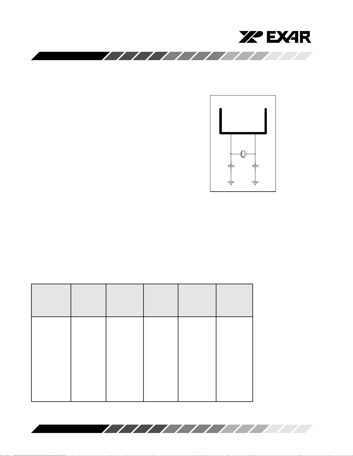
cessor crystal (parallel resonant/ 22-33 pF load) is
connected externally between the XTAL1 and
XTAL2 pins (see figure 8). Alternatively, an external
clock can be connected to the XTAL1 pin to clock
the internal baud rate generator for standard or
custom rates. (see Baud Rate Generator Program-
ming).
Rev. 3.10
13
Page 14
ST16C554/554D/68C554
The generator divides the input 16X clock by any
divisor from 1 to 216 -1. The 554D divides the basic
crystal or external clock by 16. Further division of this
16X clock provides two table rates to support low and
high data rate applications using the same system
design. Customized Baud Rates can be achieved by
selecting the proper divisor values for the MSB and
LSB sections of baud rate generator.
Programming the Baud Rate Generator Registers
DLM (MSB) and DLL (LSB) provides a user capability
for selecting the desired final baud rate. The example
in Table 5 below, shows the two selectable baud rate
tables available when using a 7.3728 MHz crystal.
Figure 8, Crystal oscillator connection
XTAL 1
C1
22pF
X1
1.8432 MHz
XTAL 2
C2
33pF
Table 5, BAUD RATE GENERATOR PROGRAMMING TABLE:
Output Output User User DLM DLL
Baud Rate Baud Rate 16 x Clock 16 x Clock Program Program
(1.8432 MHz (7.3728 MHz Divisor Divisor Value Value
Clock) Clock) (Decimal) (HEX) (HEX) (HEX)
50 200 2304 900 09 00
300 1200 384 180 01 80
600 2400 192 C0 00 C0
1200 4800 96 60 00 60
2400 9600 48 30 00 30
4800 19.2K 24 18 00 18
9600 38.4k 12 0C 00 0C
19.2k 76.8k 6 06 00 06
38.4k 153.6k 3 03 00 03
57.6k 230.4k 2 02 00 02
115.2k 460.8k 1 01 00 01
Rev. 3.10
14
Page 15

ST16C554/554D/68C554
DMA Operation
The 554D FIFO trigger level provides additional
flexibility to the user for block mode operation. LSR
bits 5-6 provide an indication when the transmitter is
empty or has an empty location(s). The user can
optionally operate the transmit and receive FIFOs in
the DMA mode (FCR bit-3). When the transmit and
receive FIFOs are enabled and the DMA mode is
deactivated (DMA Mode 0), the 554D activates the
interrupt output pin for each data transmit or receive
operation. When DMA mode is activated (DMA Mode
1), the user takes the advantage of block mode
operation by loading or unloading the FIFO in a block
sequence determined by the preset trigger level. In
this mode, the 554D sets the interrupt output pin when
characters in the transmit FIFOs are below the trans-
mit trigger level, or the characters in the receive FIFOs
are above the receive trigger level.
Loopback Mode
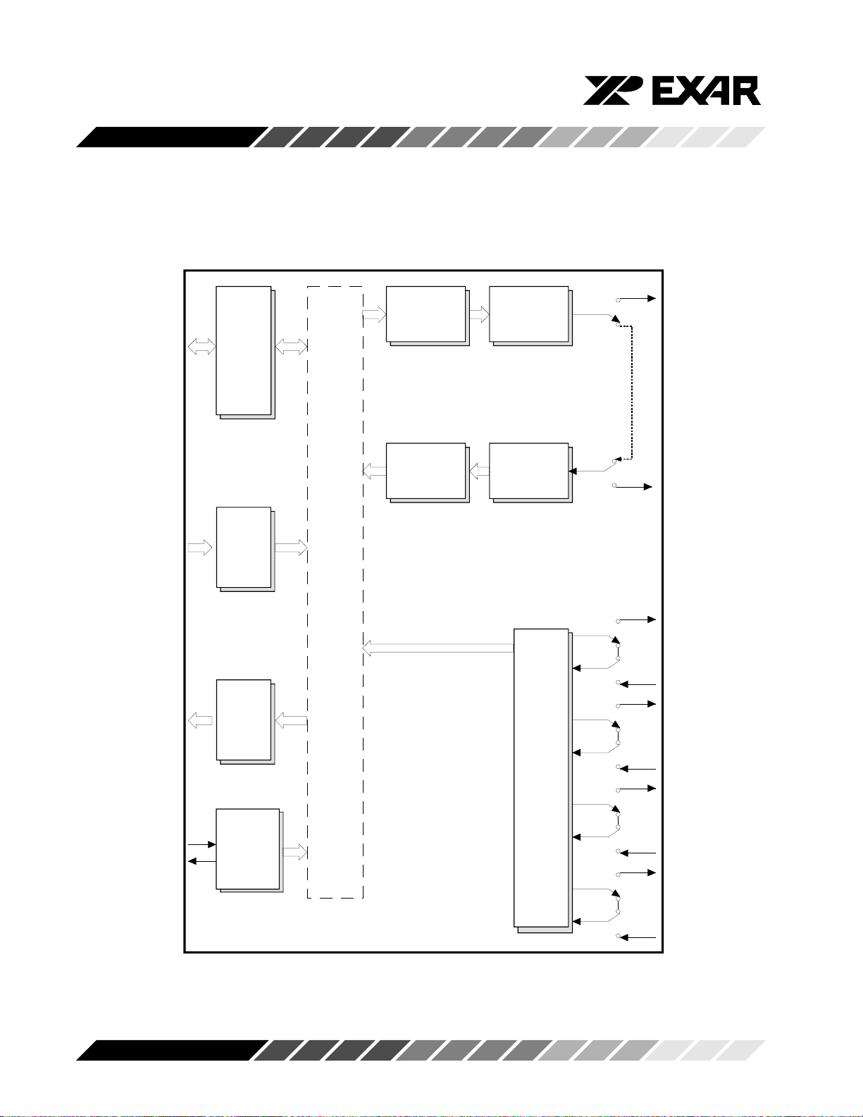
The internal loopback capability allows onboard diag-
nostics. In the loopback mode the normal modem
interface pins are disconnected and reconfigured for
loopback internally. MCR register bits 0-3 are used for
controlling loopback diagnostic testing. In the
loopback mode OP1 and OP2 in the MCR register
(bits 3/2) control the modem -RI and -CD inputs
respectively. MCR signals -DTR and -RTS (bits 0-1)
are used to control the modem -CTS and -DSR inputs
respectively. The transmitter output (TX) and the
receiver input (RX) are disconnected from their asso-
ciated interface pins, and instead are connected to-
gether internally (See Figure 12). The -CTS, -DSR, -
CD, and -RI are disconnected from their normal
modem control inputs pins, and instead are connected
internally to -DTR, -RTS, -OP1 and -OP2. Loopback
test data is entered into the transmit holding register
via the user data bus interface, D0-D7. The transmit
UART serializes the data and passes the serial data to
the receive UART via the internal loopback connec-
tion. The receive UART converts the serial data back
into parallel data that is then made available at the
user data interface, D0-D7. The user optionally com-
pares the received data to the initial transmitted data
for verifying error free operation of the UART TX/RX
circuits.
In this mode, the receiver and transmitter interrupts
are fully operational. The Modem Control Interrupts
are also operational. However, the interrupts can only
be read using lower four bits of the Modem Control
Register (MCR bits 0-3) instead of the four Modem
Status Register bits 4-7. The interrupts are still con-
trolled by the IER.
Rev. 3.10
15
Page 16
ST16C554/554D/68C554
Figure 12, INTERNAL LOOPBACK MODE DIAGRAM
D0-D7
-IOR,-IOW
RESET
A0-A2
-CS A-D
INT A-D
-RXRDY
-TXRDY
Transmit
FIFO
Registers
&
Data bus
Control Logic
Receive
FIFO
Registers
Logic
Select
Register
&
Control signals
Inter Connect Bus Lines
Logic
Control
Interrupt
Transmit
Shift
Register
Receive
Shift
Register
TX A-D
MCR Bit-4=1
RX A-D
-RTS A-D
-CD A-D
-DTR A-D
XTAL1
XTAL2
Rev. 3.10
-RI A-D
(-OP1 A-D)
Modem Control Logic
&
Clock
Generator
Baud Rate
16
-DSR A-D
(-OP2 A-D)
-CTS A-D
Page 17
ST16C554/554D/68C554
REGISTER FUNCTIONAL DESCRIPTIONS
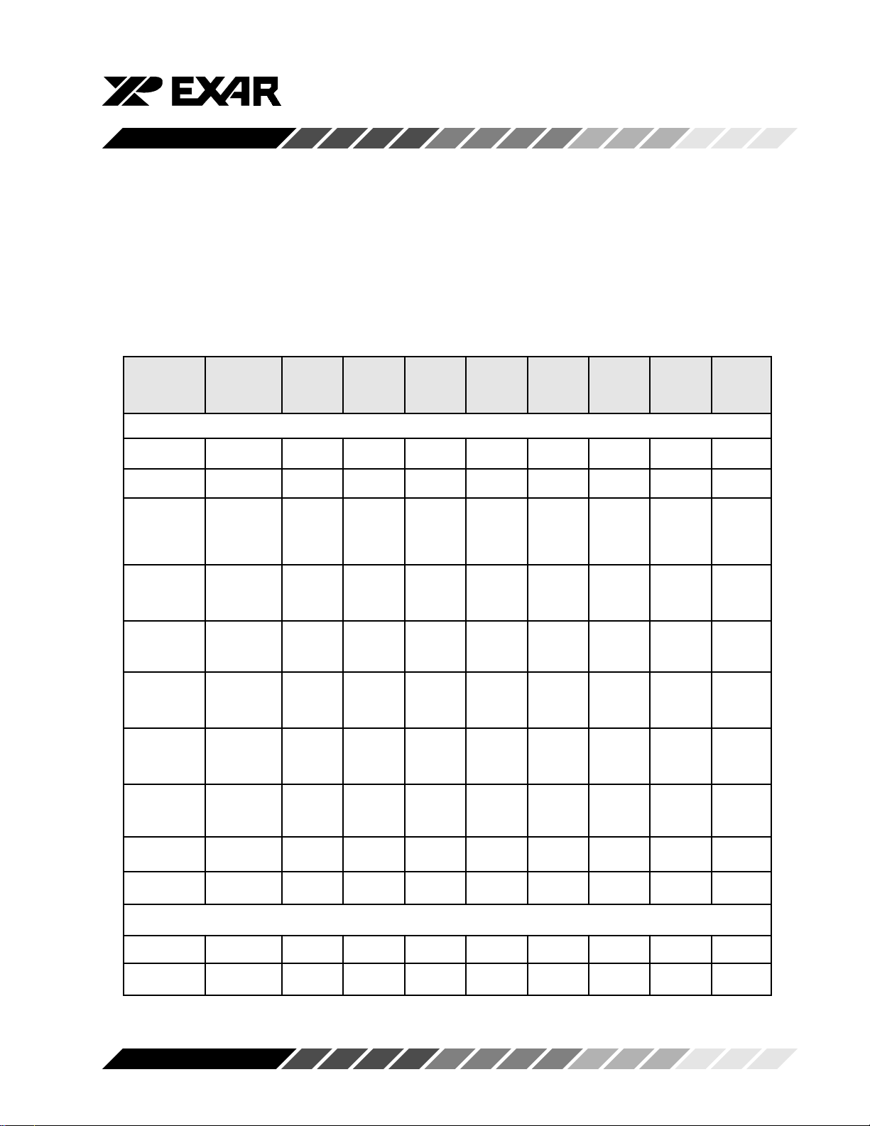
The following table delineates the assigned bit functions for the fifteen 554D internal registers. The assigned
bit functions are more fully defined in the following paragraphs.
Table 6, ST16C554D INTERNAL REGISTERS
A2 A1 A0 Register BIT-7 BIT-6 BIT-5 BIT-4 BIT-3 BIT-2 BIT-1 BIT-0
[Note *5]
General Register Set
0 0 0 RHR[XX] bit-7 bit-6 bit-5 bit-4 bit-3 bit-2 bit-1 bit-0
0 0 0 THR[XX] bit-7 bit-6 bit-5 bit-4 bit-3 bit-2 bit-1 bit-0
0 0 1 IER[00] 0000modem receive transmit receive
0 1 0 FCR RCVR RCVR 0 0 DMA XMIT RCVR FIFO
trigger trigger mode FIFO FIFO enable
(MSB) (LSB) select reset reset
0 1 0 ISR[01] FIFOs FIFOs 0 0 INT INT INT INT
enabled enabled priority priority priority status
0 1 1 LCR[00] divisor set set even parity stop word word
latch break parity parity enable bits length length
enable bit-1 bit-0
1 0 0 MCR[00] 0 0 0 loop -OP2/ -OP1 -RTS -DTR
back INTx
status line holding holding
interrupt status register register
interrupt
bit-2 bit-1 bit-0
enable
1 0 1 LSR[60] FIFO trans. trans. break framing parity overrun receive
1 1 0 MSR[X0] CD RI DSR CTS delta delta delta delta
1 1 1 SPR[FF] bit-7 bit-6 bit-5 bit-4 bit-3 bit-2 bit-1 bit-0
data empty holding interrupt error error error data
error empty ready
-CD -RI -DSR -CTS
Special Register set: Note *2
0 0 0 DLL[XX] bit-7 bit-6 bit-5 bit-4 bit-3 bit-2 bit-1 bit-0
0 0 1 DLM[XX] bit-15 bit-14 bit-13 bit-12 bit-11 bit-10 bit-9 bit-8
Note *2: The Special register set is accessible only when LCR bit-7 is set to 1.
Rev. 3.10
17
Page 18

ST16C554/554D/68C554
Note *5: The value between the square brackets
represents the registers initialized HEX value.
Transmit (THR) and Receive (RHR) Holding Reg-
isters
A) The receive data available interrupts are issued to
the external CPU when the FIFO has reached the
programmed trigger level. It will be cleared when the
FIFO drops below the programmed trigger level.
The serial transmitter section consists of an 8-bit
Transmit Hold Register (THR) and Transmit Shift
Register (TSR). The status of the THR is provided in
the Line Status Register (LSR). Writing to the THR
transfers the contents of the data bus (D7-D0) to the
THR, providing that the THR or TSR is empty. The
THR empty flag in the LSR register will be set to a logic
1 when the transmitter is empty or when data is
transferred to the TSR. Note that a write operation can
be performed when the transmit holding register
empty flag is set (logic 0 = FIFO full, logic 1= at least
one FIFO location available).
The serial receive section also contains an 8-bit
Receive Holding Register, RHR. Receive data is
removed from the 554D and receive FIFO by reading
the RHR register. The receive section provides a
mechanism to prevent false starts. On the falling edge
of a start or false start bit, an internal receiver counter
starts counting clocks at 16x clock rate. After 7 1/2
clocks the start bit time should be shifted to the center
of the start bit. At this time the start bit is sampled and
if it is still a logic 0 it is validated. Evaluating the start
bit in this manner prevents the receiver from assem-
bling a false character. Receiver status codes will be
posted in the LSR.
Interrupt Enable Register (IER)
B) FIFO status will also be reflected in the user
accessible ISR register when the FIFO trigger level is
reached. Both the ISR register status bit and the
interrupt will be cleared when the FIFO drops below
the trigger level.
C) The data ready bit (LSR BIT-0) is set as soon as a
character is transferred from the shift register to the
receive FIFO. It is reset when the FIFO is empty.
IER Vs Receive/Transmit FIFO Polled Mode Op-
eration
When FCR BIT-0 equals a logic 1; resetting IER bits
0-3 enables the 554D in the FIFO polled mode of
operation. Since the receiver and transmitter have
separate bits in the LSR either or both can be used in
the polled mode by selecting respective transmit or
receive control bit(s).
A) LSR BIT-0 will be a logic 1 as long as there is one
byte in the receive FIFO.
B) LSR BIT 1-4 will provide the type of errors encoun-
tered, if any.
C) LSR BIT-5 will indicate when the transmit FIFO is
empty.
The Interrupt Enable Register (IER) masks the inter-
rupts from receiver ready, transmitter empty, line
status and modem status registers. These interrupts
would normally be seen on the INT A-D output pins in
the 16 mode, or on WIRE-OR IRQ output pin, in the 68
mode.
IER Vs Receive FIFO Interrupt Mode Operation
When the receive FIFO (FCR BIT-0 = a logic 1) and
receive interrupts (IER BIT-0 = logic 1) are enabled,
the receive interrupts and register status will reflect
the following:
Rev. 3.10
D) LSR BIT-6 will indicate when both the transmit
FIFO and transmit shift register are empty.
E) LSR BIT-7 will indicate any FIFO data errors.
IER BIT-0:
This interrupt will be issued when the FIFO has
reached the programmed trigger level or is cleared
when the FIFO drops below the trigger level in the
FIFO mode of operation.
Logic 0 = Disable the receiver ready interrupt. (normal
18
Page 19

ST16C554/554D/68C554
default condition)
Logic 1 = Enable the receiver ready interrupt.
IER BIT-1:
This interrupt will be issued whenever the THR is
empty and is associated with bit-1 in the LSR register.
Logic 0 = Disable the transmitter empty interrupt.
(normal default condition)
Logic 1 = Enable the transmitter empty interrupt.
IER BIT-2:
This interrupt will be issued whenever a fully as-
sembled receive character is transferred from the
RSR to the RHR/FIFO, i.e., data ready, LSR bit-0.
Logic 0 = Disable the receiver line status interrupt.
(normal default condition)
Logic 1 = Enable the receiver line status interrupt.
IER BIT-3:
Logic 0 = Disable the modem status register interrupt.
(normal default condition)
Logic 1 = Enable the modem status register interrupt.
IER BIT 4-7:
Not used - Initialized to a logic 0.
FIFO Control Register (FCR)
This register is used to enable the FIFOs, clear the
FIFOs, set the transmit/receive FIFO trigger levels,
and select the DMA mode. The DMA, and FIFO
modes are defined as follows:
DMA MODE
Mode 0 Set and enable the interrupt for each
single transmit or receive operation, and is similar to
the ST16C454 mode. Transmit Ready (-TXRDY) will
go to a logic 0 when ever an empty transmit space is
available in the Transmit Holding Register (THR).
Receive Ready (-RXRDY) will go to a logic 0 when-
ever the Receive Holding Register (RHR) is loaded
with a character.
Mode 1 Set and enable the interrupt in a block
mode operation. The transmit interrupt is set when the
transmit FIFO is below the programmed trigger level.
-TXRDY remains a logic 0 as long as one empty FIFO
location is available. The receive interrupt is set when
the receive FIFO fills to the programmed trigger level.
However the FIFO continues to fill regardless of the
programmed level until the FIFO is full. -RXRDY
remains a logic 0 as long as the FIFO fill level is above
the programmed trigger level.
FCR BIT-0:
Logic 0 = Disable the transmit and receive FIFO.
(normal default condition)
Logic 1 = Enable the transmit and receive FIFO. This
bit must be a 1 when other FCR bits are written to or
they will not be programmed.
FCR BIT-1:
Logic 0 = No FIFO receive reset. (normal default
condition)
Logic 1 = Clears the contents of the receive FIFO and
resets the FIFO counter logic (the receive shift regis-
ter is not cleared or altered). This bit will return to a
logic 0 after clearing the FIFO.
FCR BIT-2:
Logic 0 = No FIFO transmit reset. (normal default
condition)
Logic 1 = Clears the contents of the transmit FIFO and
resets the FIFO counter logic (the transmit shift regis-
ter is not cleared or altered). This bit will return to a
logic 0 after clearing the FIFO.
FCR BIT-3:
Logic 0 = Set DMA mode 0. (normal default condi-
tion)
Logic 1 = Set DMA mode 1.
Transmit operation in mode 0:
When the 554D is in the ST16C450 mode (FIFOs
disabled, FCR bit-0 = logic 0) or in the FIFO mode
(FIFOs enabled, FCR bit-0 = logic 1, FCR bit-3 = logic
0) and when there are no characters in the transmit
FIFO or transmit holding register, the -TXRDY pin will
be a logic 0. Once active the -TXRDY pin will go to a
logic 1 after the first character is loaded into the
transmit holding register.
Receive operation in mode 0:
When the 554D is in mode 0 (FCR bit-0 = logic 0) or
in the FIFO mode (FCR bit-0 = logic 1, FCR bit-3 =
logic 0) and there is at least one character in the
receive FIFO, the -RXRDY pin will be a logic 0. Once
active the -RXRDY pin will go to a logic 1 when there
are no more characters in the receiver.
Rev. 3.10
19
Page 20
ST16C554/554D/68C554
Transmit operation in mode 1:
When the 554D is in FIFO mode ( FCR bit-0 = logic 1,
FCR bit-3 = logic 1 ), the -TXRDY pin will be a logic 1
when the transmit FIFO is completely full. It will be a
logic 0 if one or more FIFO locations are empty.
Receive operation in mode 1:
When the 554D is in FIFO mode (FCR bit-0 = logic 1,
FCR bit-3 = logic 1) and the trigger level has been
reached, or a Receive Time Out has occurred, the -
RXRDY pin will go to a logic 0. Once activated, it will
go to a logic 1 after there are no more characters in the
FIFO.
FCR BIT 4-5:
Not used - Initialized to a logic 0.
FCR BIT 6-7: (logic 0 or cleared is the default condi-
tion, Rx trigger level = 1)
These bits are used to set the trigger level for the
receive FIFO interrupt.
An interrupt is generated when the number of charac-
ters in the FIFO equals the programmed trigger level.
However the FIFO will continue to be loaded until it is
full.
Interrupt Status Register (ISR)
The 554D provides four levels of prioritized interrupts
to minimize external software interaction. The Inter-
rupt Status Register (ISR) provides the user with six
interrupt status bits. Performing a read cycle on the
ISR will provide the user with the highest pending
interrupt level to be serviced. No other interrupts are
acknowledged until the pending interrupt is serviced.
Whenever the interrupt status register is read, the
interrupt status is cleared. However it should be noted
that only the current pending interrupt is cleared by the
read. A lower level interrupt may be seen after reread-
ing the interrupt status bits. The Interrupt Source
Table 7 (below) shows the data values (bit 0-5) for the
four prioritized interrupt levels and the interrupt
sources associated with each of these interrupt levels:
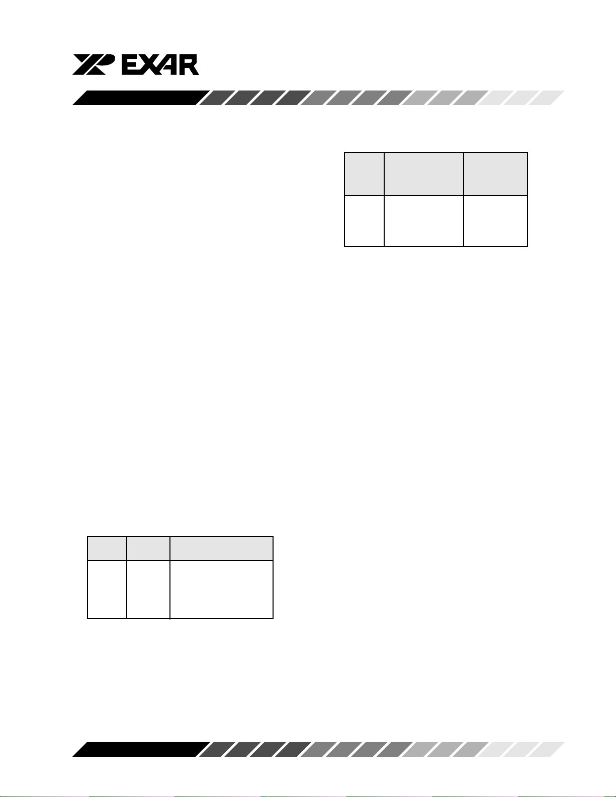
BIT-7 BIT-6 RX FIFO trigger level
00 1
01 4
10 8
11 14
Table 7, INTERRUPT SOURCE TABLE
Priority [ ISR BITS ]
Level Bit-5 Bit-4 Bit-3 Bit-2 Bit-1 Bit-0 Source of the interrupt
1 000110 LSR (Receiver Line Status Register)
2 000100 RXRDY (Received Data Ready)
2 001100 RXRDY (Receive Data time out)
3 000010 TXRDY ( Transmitter Holding Register Empty)
4 000000 MSR (Modem Status Register)
Rev. 3.10
20
Page 21
ST16C554/554D/68C554
ISR BIT-0:
Logic 0 = An interrupt is pending and the ISR contents
may be used as a pointer to the appropriate interrupt
service routine.
Logic 1 = No interrupt pending. (normal default condi-
tion)
ISR BIT 1-3: (logic 0 or cleared is the default condition)
These bits indicate the source for a pending interrupt
at interrupt priority levels 1, 2, and 3 (See Interrupt
Source Table).
ISR BIT 4-5:
Not used - Initialized to a logic 0.
ISR BIT 6-7: (logic 0 or cleared is the default condition)
These bits are set to a logic 0 when the FIFO is not
being used. They are set to a logic 1 when the FIFOs
are enabled.
Line Control Register (LCR)
The Line Control Register is used to specify the
asynchronous data communication format. The word
length, the number of stop bits, and the parity are
selected by writing the appropriate bits in this register.
LCR BIT 0-1: (logic 0 or cleared is the default condi-
tion)
These two bits specify the word length to be transmit-
ted or received.
BIT-1 BIT-0 Word length
00 5
01 6
10 7
11 8
BIT-2 Word length Stop bit
length
(Bit time(s))
0 5,6,7,8 1
1 5 1-1/2
1 6,7,8 2
LCR BIT-3:
Parity or no parity can be selected via this bit.
Logic 0 = No parity. (normal default condition)
Logic 1 = A parity bit is generated during the transmis-
sion, receiver checks the data and parity for transmis-
sion errors.
LCR BIT-4:
If the parity bit is enabled with LCR bit-3 set to a logic
1, LCR BIT-4 selects the even or odd parity format.
Logic 0 = ODD Parity is generated by forcing an odd
number of logic 1s in the transmitted data. The
receiver must be programmed to check the same
format. (normal default condition)
Logic 1 = EVEN Parity is generated by forcing an even
the number of logic 1s in the transmitted. The receiver
must be programmed to check the same format.
LCR BIT-5:
If the parity bit is enabled, LCR BIT-5 selects the
forced parity format.
LCR BIT-5 = logic 0, parity is not forced. (normal
default condition)
LCR BIT-5 = logic 1 and LCR BIT-4 = logic 0, parity bit
is forced to a logical 1 for the transmit and receive
data.
LCR BIT-5 = logic 1 and LCR BIT-4 = logic 1, parity bit
is forced to a logical 0 for the transmit and receive
data.
LCR BIT-2: (logic 0 or cleared is the default condition)
The length of stop bit is specified by this bit in
conjunction with the programmed word length.
Rev. 3.10
21
Page 22
ST16C554/554D/68C554
Logic 0 = Forces INT (A-D) outputs to the three state
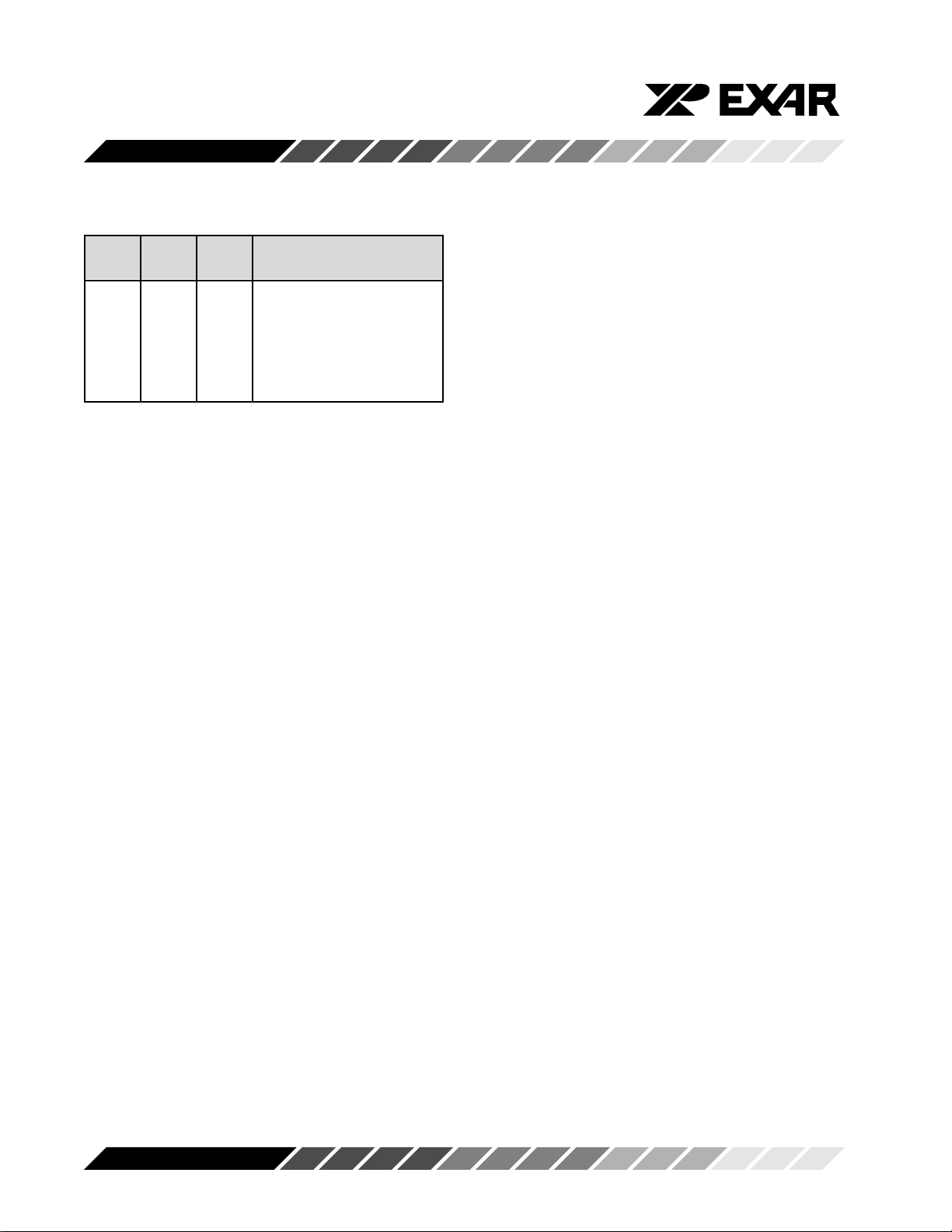
LCR LCR LCR Parity selection
Bit-5 Bit-4 Bit-3
X X 0 No parity
0 0 1 Odd parity
0 1 1 Even parity
1 0 1 Force parity 1
1 1 1 Forced parity 0
LCR BIT-6:
When enabled the Break control bit causes a break
condition to be transmitted (the TX output is forced to
a logic 0 state). This condition exists until disabled by
setting LCR bit-6 to a logic 0.
Logic 0 = No TX break condition. (normal default
condition)
Logic 1 = Forces the transmitter output (TX) to a logic
0 for alerting the remote receiver to a line break
condition.
LCR BIT-7:
Not used - Initialized to a logic 0.
Modem Control Register (MCR)
This register controls the interface with the modem or
a peripheral device.
MCR BIT-0:
Logic 0 = Force -DTR output to a logic 1. (normal
default condition)
Logic 1 = Force -DTR output to a logic 0.
MCR BIT-1:
Logic 0 = Force -RTS output to a logic 1. (normal
default condition)
Logic 1 = Force -RTS output to a logic 0.
MCR BIT-2:
This bit is used in the Loopback mode only. In the
loopback mode this bit is use to write the state of the
modem -RI interface signal via -OP1.
MCR BIT-3: (Used to control the modem -CD signal
in the loopback mode.)
mode during the 16 mode. (normal default condition)
In the Loopback mode, sets -OP2 (-CD) internally to a
logic 1.
Logic 1 = Forces the INT (A-D) outputs to the active
mode during the 16 mode. In the Loopback mode, sets
-OP2 (-CD) internally to a logic 0.
MCR BIT-4:
Logic 0 = Disable loopback mode. (normal default
condition)
Logic 1 = Enable local loopback mode (diagnostics).
MCR BIT 5-7:
Not used - Initialized to a logic 0.
Line Status Register (LSR)
This register provides the status of data transfers
between. the 554D and the CPU.
LSR BIT-0:
Logic 0 = No data in receive holding register or FIFO.
(normal default condition)
Logic 1 = Data has been received and is saved in the
receive holding register or FIFO.
LSR BIT-1:
Logic 0 = No overrun error. (normal default condition)
Logic 1 = Overrun error. A data overrun error occurred
in the receive shift register. This happens when addi-
tional data arrives while the FIFO is full. In this case
the previous data in the shift register is overwritten.
Note that under this condition the data byte in the
receive shift register is not transfered into the FIFO,
therefore the data in the FIFO is not corrupted by the
error.
LSR BIT-2:
Logic 0 = No parity error. (normal default condition)
Logic 1 = Parity error. The receive character does not
have correct parity information and is suspect. In the
FIFO mode, this error is associated with the character
at the top of the FIFO.
LSR BIT-3:
Logic 0 = No framing error. (normal default condition)
Logic 1 = Framing error. The receive character did not
Rev. 3.10
22
Page 23

ST16C554/554D/68C554
have a valid stop bit(s). In the FIFO mode this error is
associated with the character at the top of the FIFO.
LSR BIT-4:
Logic 0 = No break condition. (normal default condi-
tion)
Logic 1 = The receiver received a break signal (RX
was a logic 0 for one character frame time). In the
FIFO mode, only one break character is loaded into
the FIFO.
LSR BIT-5:
This bit is the Transmit Holding Register Empty indi-
cator. This bit indicates that the UART is ready to
accept a new character for transmission. In addition,
this bit causes the UART to issue an interrupt to CPU
when the THR interrupt enable is set. The THR bit is
set to a logic 1 when a character is transferred from the
transmit holding register into the transmitter shift
register. The bit is reset to logic 0 concurrently with the
loading of the transmitter holding register by the CPU.
In the FIFO mode this bit is set when the transmit FIFO
is empty; it is cleared when at least 1 byte is written to
the transmit FIFO.
LSR BIT-6:
This bit is the Transmit Empty indicator. This bit is set
to a logic 1 whenever the transmit holding register and
the transmit shift register are both empty. It is reset to
logic 0 whenever either the THR or TSR contains a
data character. In the FIFO mode this bit is set to one
whenever the transmit FIFO and transmit shift register
are both empty.
LSR BIT-7:
Logic 0 = No Error. (normal default condition)
Logic 1 = At least one parity error, framing error or
break indication is in the current FIFO data. This bit is
cleared when LSR register is read.
Modem Status Register (MSR)
This register provides the current state of the control
interface signals from the modem, or other peripheral
device that the 554D is connected to. Four bits of this
register are used to indicate the changed information.
These bits are set to a logic 1 whenever a control input
from the modem changes state. These bits are set to
a logic 0 whenever the CPU reads this register.
MSR BIT-0:
Logic 0 = No -CTS Change (normal default condition)
Logic 1 = The -CTS input to the 554D has changed
state since the last time it was read. A modem Status
Interrupt will be generated.
MSR BIT-1:
Logic 0 = No -DSR Change. (normal default condition)
Logic 1 = The -DSR input to the 554D has changed
state since the last time it was read. A modem Status
Interrupt will be generated.
MSR BIT-2:
Logic 0 = No -RI Change. (normal default condition)
Logic 1 = The -RI input to the 554D has changed from
a logic 0 to a logic 1. A modem Status Interrupt will be
generated.
MSR BIT-3:
Logic 0 = No -CD Change. (normal default condition)
Logic 1 = Indicates that the -CD input to the has
changed state since the last time it was read. A
modem Status Interrupt will be generated.
MSR BIT-4:
-CTS (active high, logical 1). Normally MSR bit-4 bit
is the compliment of the -CTS input. However in the
loopback mode, this bit is equivalent to the RTS bit in
the MCR register.
MSR BIT-5:
DSR (active high, logical 1). Normally this bit is the
compliment of the -DSR input. In the loopback mode,
this bit is equivalent to the DTR bit in the MCR register.
MSR BIT-6:
RI (active high, logical 1). Normally this bit is the
compliment of the -RI input. In the loopback mode this
bit is equivalent to the OP1 bit in the MCR register.
Rev. 3.10
23
Page 24
ST16C554/554D/68C554
MSR BIT-7:
CD (active high, logical 1). Normally this bit is the
compliment of the -CD input. In the loopback mode
this bit is equivalent to the OP2 bit in the MCR register.
Scratchpad Register (SPR)
The ST16C554D provides a temporary data register
to store 8 bits of user information.
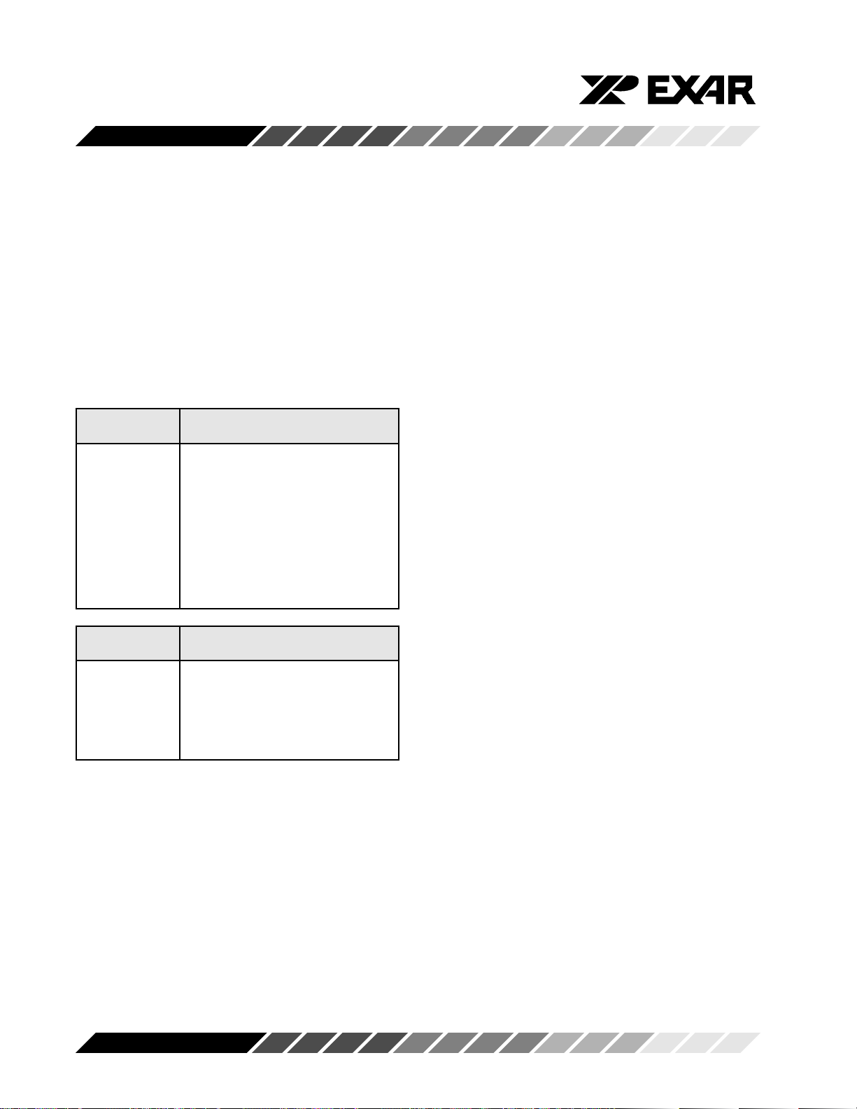
ST16C554D EXTERNAL RESET CONDITIONS
REGISTERS RESET STATE
IER IER BITS 0-7=0
ISR ISR BIT-0=1, ISR BITS 1-7=0
LCR LCR BITS 0-7=0
MCR MCR BITS 0-7=0
LSR LSR BITS 0-4=0,
LSR BITS 5-6=1 LSR, BIT 7=0
MSR MSR BITS 0-3=0,
MSR BITS 4-7= input signals
FCR FCR BITS 0-7=0
SIGNALS RESET STATE
TX A-D High
-RTS A-D High
-DTR A-D High
-RXRDY High
-TXRDY Low
Rev. 3.10
24
Page 25
ST16C554/554D/68C554
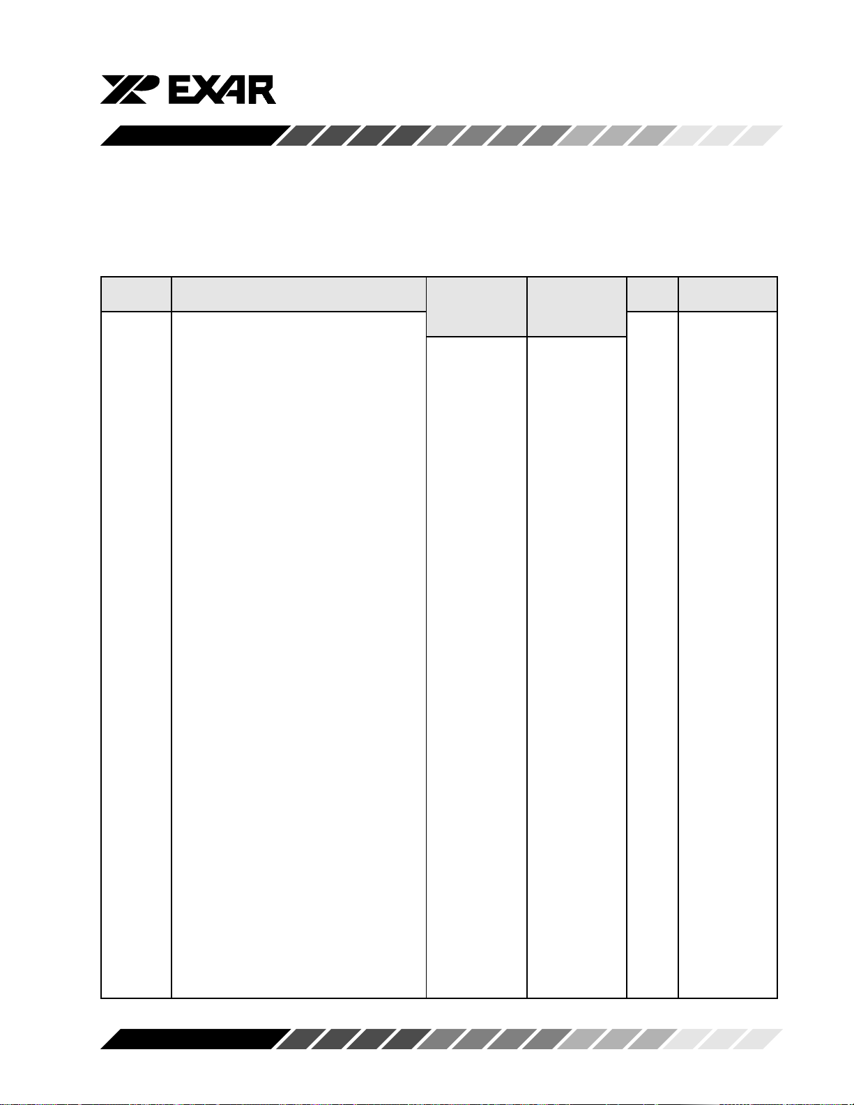
AC ELECTRICAL CHARACTERISTICS
TA=0° - 70°C (-40° - +85°C for Industrial grade packages), Vcc=3.3 - 5.0 V ± 10% unless otherwise specified.
Symbol Parameter Limits Limits Units Conditions
3.3 5.0
Min Max Min Max
T1w,T2w Clock pulse duration 17 17 ns
T3w Oscillator/Clock frequency 8 24 MHz
T6s Address setup time 5 0 ns
T7d -IOR delay from chip select 10 10 ns
T7w -IOR strobe width 35 25 ns
T7h Chip select hold time from -IOR 0 0 ns
T9d Read cycle delay 40 30 ns
T12d Delay from -IOR to data 35 25 ns
T12h Data disable time 25 35 15 ns
T13d -IOW delay from chip select 10 10 ns
T13w -IOW strobe width 35 25 ns
T13h Chip select hold time from -IOW 0 0 ns
T15d Write cycle delay 40 30 ns
T16s Data setup time 20 15 ns
T16h Data hold time 5 5 ns
T17d Delay from -IOW to output 50 40 ns 100 pF load
T18d Delay to set interrupt from MODEM 40 35 ns 100 pF load
input
T19d Delay to reset interrupt from -IOR 40 35 ns 100 pF load
T20d Delay from stop to set interrupt 1 1 Rclk
T21d Delay from -IOR to reset interrupt 45 40 ns 100 pF load
T22d Delay from stop to interrupt 45 40 ns
T23d Delay from initial INT reset to transmit 8 24 8 24 Rclk
start
T24d Delay from -IOW to reset interrupt 45 40 ns
T25d Delay from stop to set -RxRdy 1 1 Rclk
T26d Delay from -IOR to reset -RxRdy 45 40 ns
T27d Delay from -IOW to set -TxRdy 45 40 ns
T28d Delay from start to reset -TxRdy 8 8 Rclk
T30s Address setup time 10 10 ns
T30w Chip select strobe width 40 40 ns
T30h Address hold time 15 15 ns
T30d Read cycle delay 70 70 ns
T31d Delay from -CS to data 15 15 ns
T31h Data disable time 15 ns
T32s Write strobe setup time 10 10 ns
T32h Write strobe hold time 10 10 ns
T32d Write cycle delay 70 70 ns
Rev. 3.10
25
Page 26
ST16C554/554D/68C554
AC ELECTRICAL CHARACTERISTICS
TA=0° - 70°C (-40° - +85°C for Industrial grade packages), Vcc=3.3 - 5.0 V ± 10% unless otherwise specified.
Symbol Parameter Limits Limits Units Conditions
3.3 5.0
Min Max Min Max
T33s Data setup time 20 15 ns
T33h Data hold time 10 10 ns
TR Reset pulse width 40 40 ns
N Baud rate devisor 1 216-1 1 216-1 Rclk
Rev. 3.10
26
Page 27
ST16C554/554D/68C554
ABSOLUTE MAXIMUM RATINGS
Supply range 7 Volts
Voltage at any pin GND - 0.3 V to VCC +0.3 V
Operating temperature -40° C to +85° C
Storage temperature -65° C to 150° C
Package dissipation 500 mW
DC ELECTRICAL CHARACTERISTICS
TA=0° - 70°C (-40° - +85°C for Industrial grade packages), Vcc=3.3 - 5.0 V ± 10% unless otherwise specified.
Symbol Parameter Limits Limits Units Conditions
3.3 5.0
Min Max Min Max
V
ILCK
V
IHCK
V
IL
V
IH
V
OL
V
OL
V
OH
V
OH
I
IL
I
CL
I
CC
C
P
Clock input low level -0.3 0.6 -0.5 0.6 V
Clock input high level 2.4 VCC 3.0 VCC V
Input low level -0.3 0.8 -0.5 0.8 V
Input high level 2.0 2.2 VCC V
Output low level on all outputs 0.4 V IOL= 5 mA
Output low level on all outputs 0.4 V IOL= 4 mA
Output high level 2.4 V IOH= -5 mA
Output high level 2.0 V IOH= -1 mA
Input leakage ±10 ±10 µA
Clock leakage ±10 ±10 µA
Avg power supply current 3 6 mA
Input capacitance 5 5 pF
RIN Internal pull-up resistance 3 15 kΩ
Note: See the Symbol Description Table, for a listing of pins having internal pull-up resistors.
Rev. 3.10
27
Page 28
ST16C554/554D/68C554
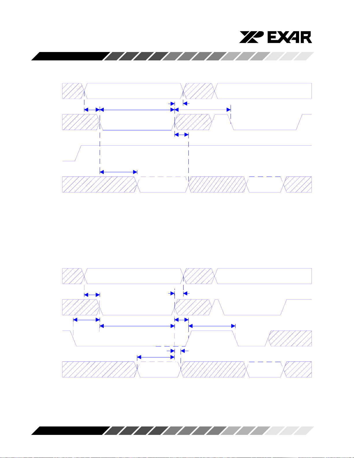
A0-A4
-CS
R/-W
D0-D7
T30s
T30w
T31d
T30h
T31h
General read timing in 68 mode
T30d
8654-RD-1
A0-A4
-CS
R/-W
D0-D7
Rev. 3.10
T32s
T30s
T30h
T32h
T30w
T33h
T33s
General write timing in 68 mode
28
T32d
8654-WD-1
Page 29
ST16C554/554D/68C554
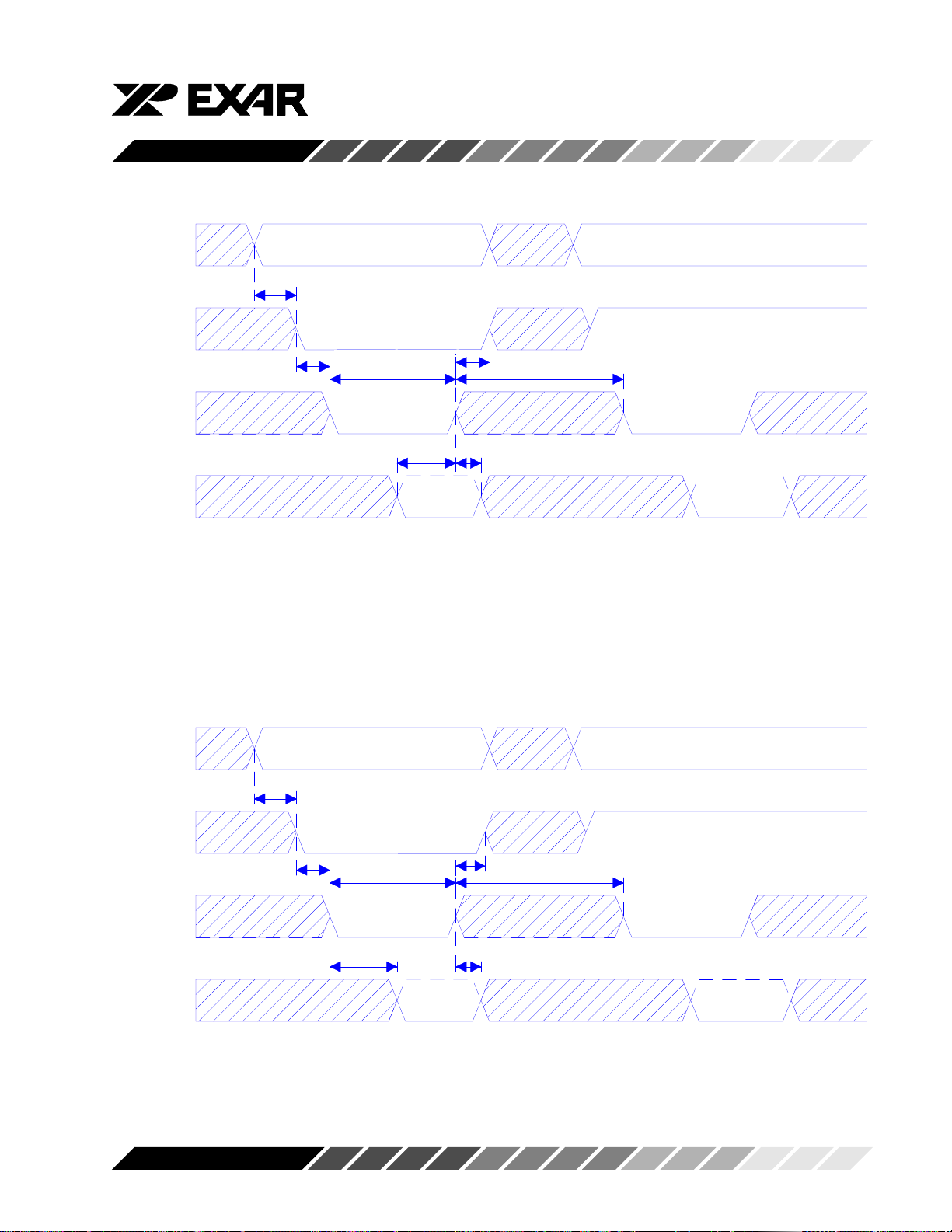
A0-A2
-CS
-IOW
D0-D7
T6s
Valid
Address
Active
T13wT13d
Active
T16s T16h
Data
T13h
T15d
General write timing in 16 mode
X552-WD-1
A0-A2
-CS
-IOR
D0-D7
Rev. 3.10
Valid
Address
T6s
Active
T7wT7d T7h T9d
Active
T12d T12h
Data
X552-RD-1
General read timing in 16 mode
29
Page 30
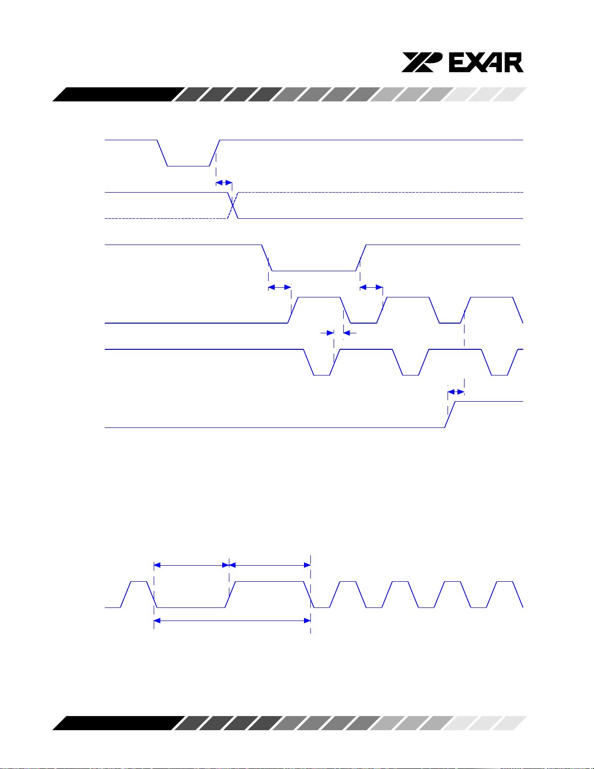
ST16C554/554D/68C554
-IOW
-RTS
-DTR
-CD
-CTS
-DSR
INT
-IOR
-RI
Active
Change of state
T17d
Change of state
Change of state
T18d T18d
Active Active
T19d
Active
Change of state
Active
Active Active
T18d
Change of state
EXTERNAL
CLOCK
T2w
Modem input/output timing
T1w
T3w
External clock timing
X552-MD-1
X654-CK-1
Rev. 3.10
30
Page 31
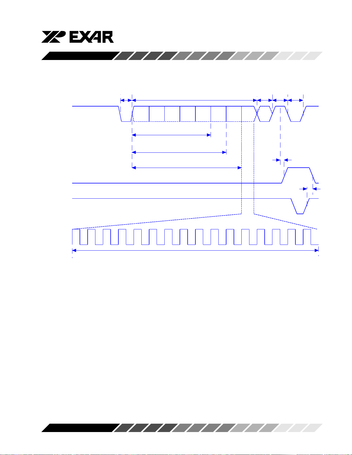
ST16C554/554D/68C554
RX
INT
-IOR
START
BIT
DATA BITS (5-8)
D0 D1 D2 D3 D4 D5 D6 D7
5 DATA BITS
6 DATA BITS
7 DATA BITS
PARITY
BIT
STOP
BIT
NEXT
DATA
START
BIT
T20d
Active
T21d
Active
16 BAUD RATE CLOCK
Receive timing
X552-RX-1
Rev. 3.10
31
Page 32
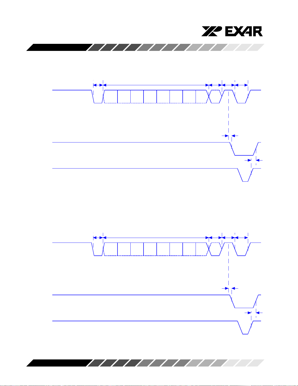
ST16C554/554D/68C554
RX
-RXRDY
-IOR
START
BIT
D0 D1 D2 D3 D4 D5 D6 D7
DATA BITS (5-8)
Receive ready timing in none FIFO mode
PARITY
BIT
STOP
BIT
NEXT
DATA
START
BIT
T25d
Active
Data
Ready
T26d
Active
X552-RX-2
RX
-RXRDY
-IOR
Rev. 3.10
START
BIT
D0 D1 D2 D3 D4 D5 D6 D7
DATA BITS (5-8)
Receive timing in FIFO mode
PARITY
BIT
STOP
BIT
First byte
that reaches
the trigger
level
T25d
Active
Data
Ready
T26d
Active
X552-RX-3
32
Page 33
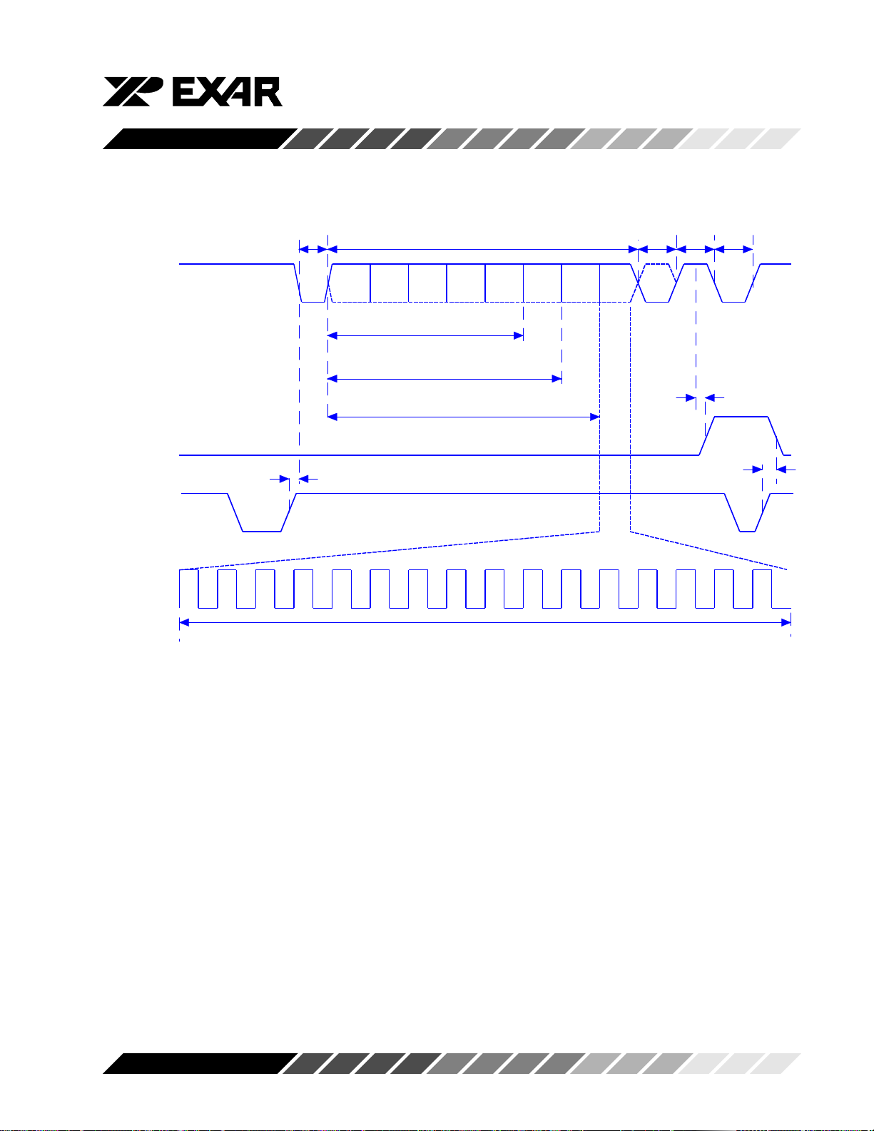
ST16C554/554D/68C554
TX
INT
-IOW
Active
START
BIT
DATA BITS (5-8)
D0 D1 D2 D3 D4 D5 D6 D7
5 DATA BITS
6 DATA BITS
7 DATA BITS
T23d
PARITY
BIT
STOP
BIT
NEXT
DATA
START
BIT
T22d
Active
Tx Ready
T24d
Active
16 BAUD RATE CLOCK
Transmit timing
X552-TX-1
Rev. 3.10
33
Page 34
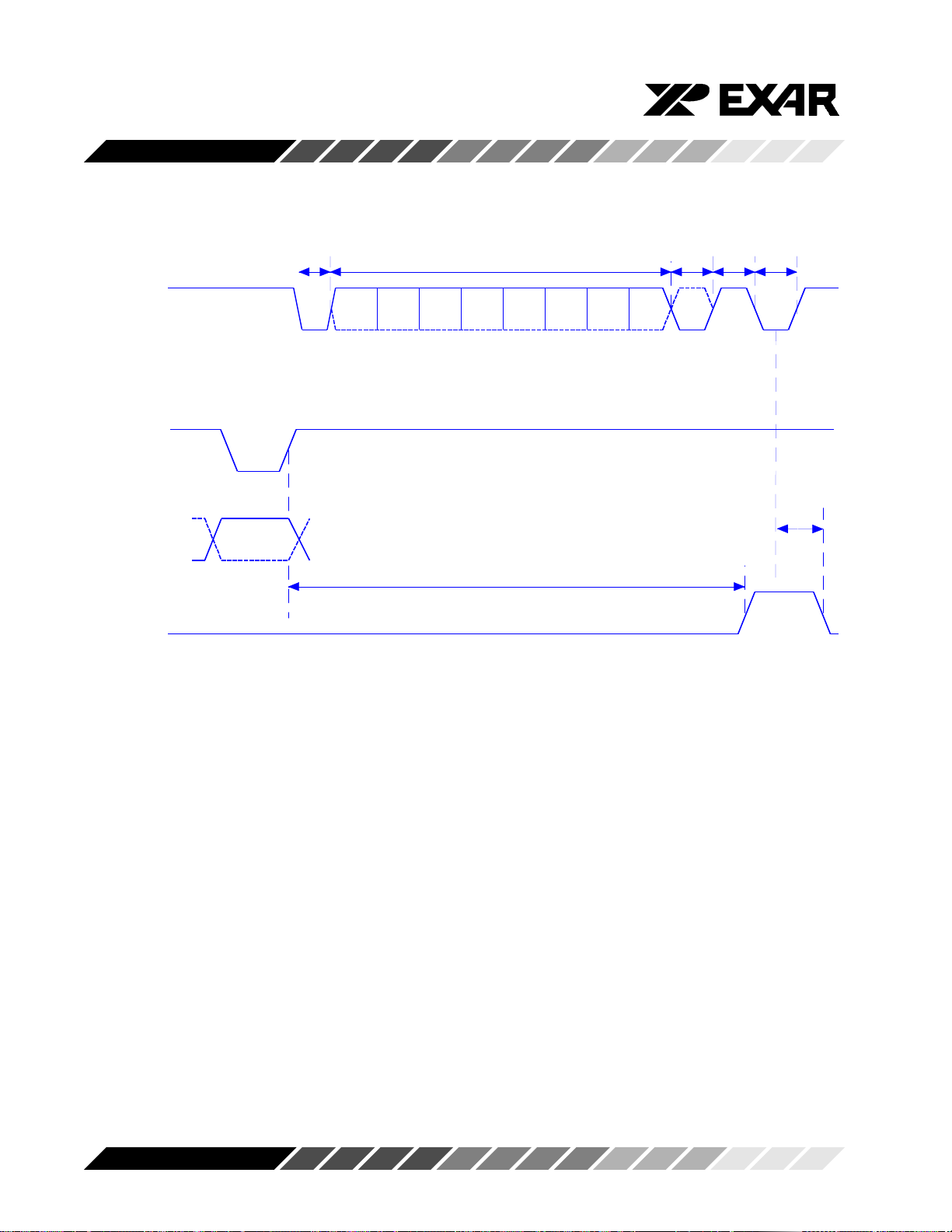
ST16C554/554D/68C554
TX
-IOW
D0-D7
-TXRDY
Active
BYTE #1
START
BIT
DATA BITS (5-8)
D0 D1 D2 D3 D4 D5 D6 D7
T27d
Active
Transmitter ready
PARITY
BIT
STOP
BIT
NEXT
DATA
START
BIT
T28d
Transmitter
not ready
X654-TX-2
Rev. 3.10
Transmit ready timing in none FIFO mode
34
Page 35
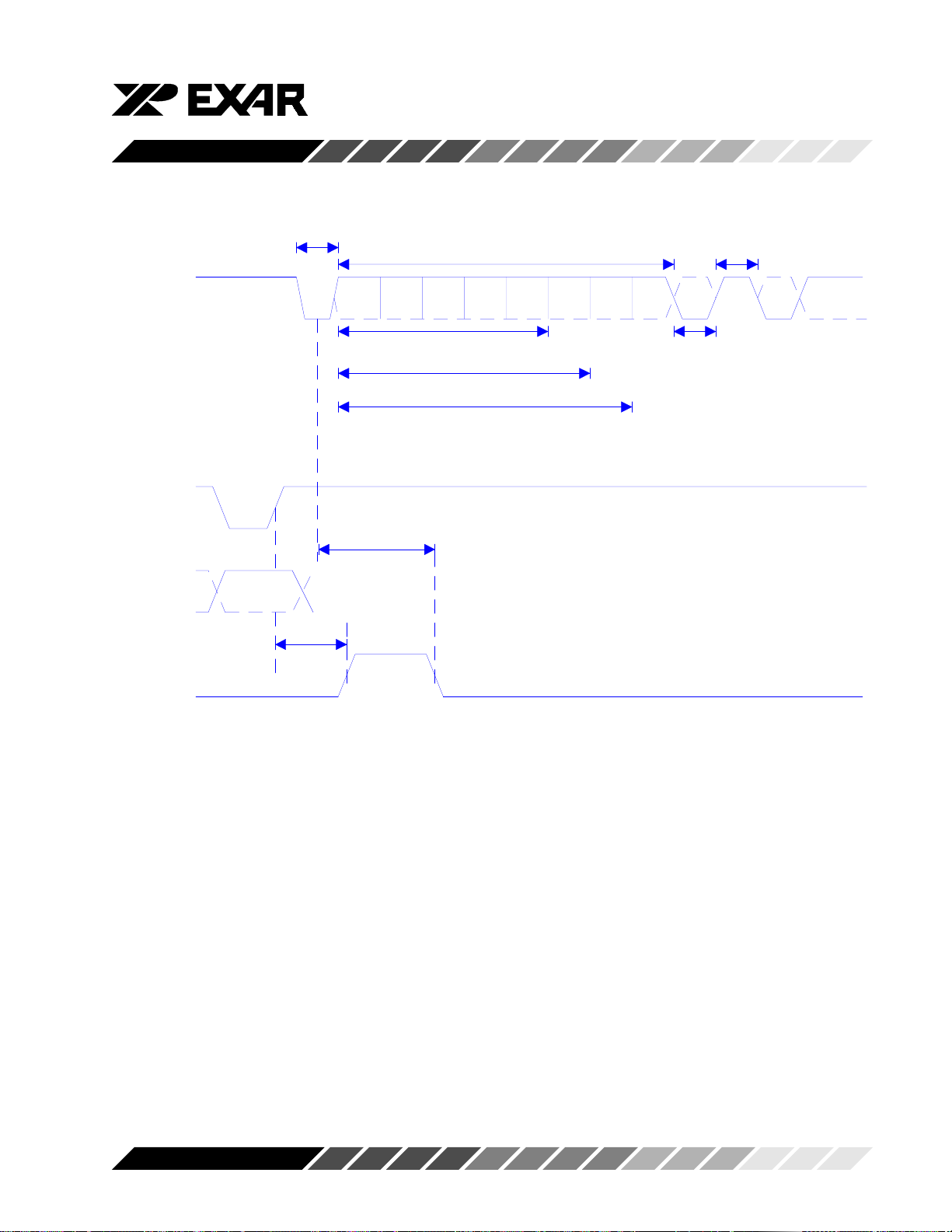
START BIT
ST16C554/554D/68C554
DATA BITS (5-8)
STOP BIT
TX
-IOW
D0-D7
-TXRDY
Active
BYTE #16
T27d
D0 D1 D2 D3 D4 D5 D6 D7
5 DATA BITS
6 DATA BITS
7 DATA BITS
T28d
FIFO Full
PARITY BIT
X552-TX-3
Rev. 3.10
Transmit ready timing in FIFO mode
35
Page 36

ST16C554/554D/68C554
Rev. 3.10
36
Page 37
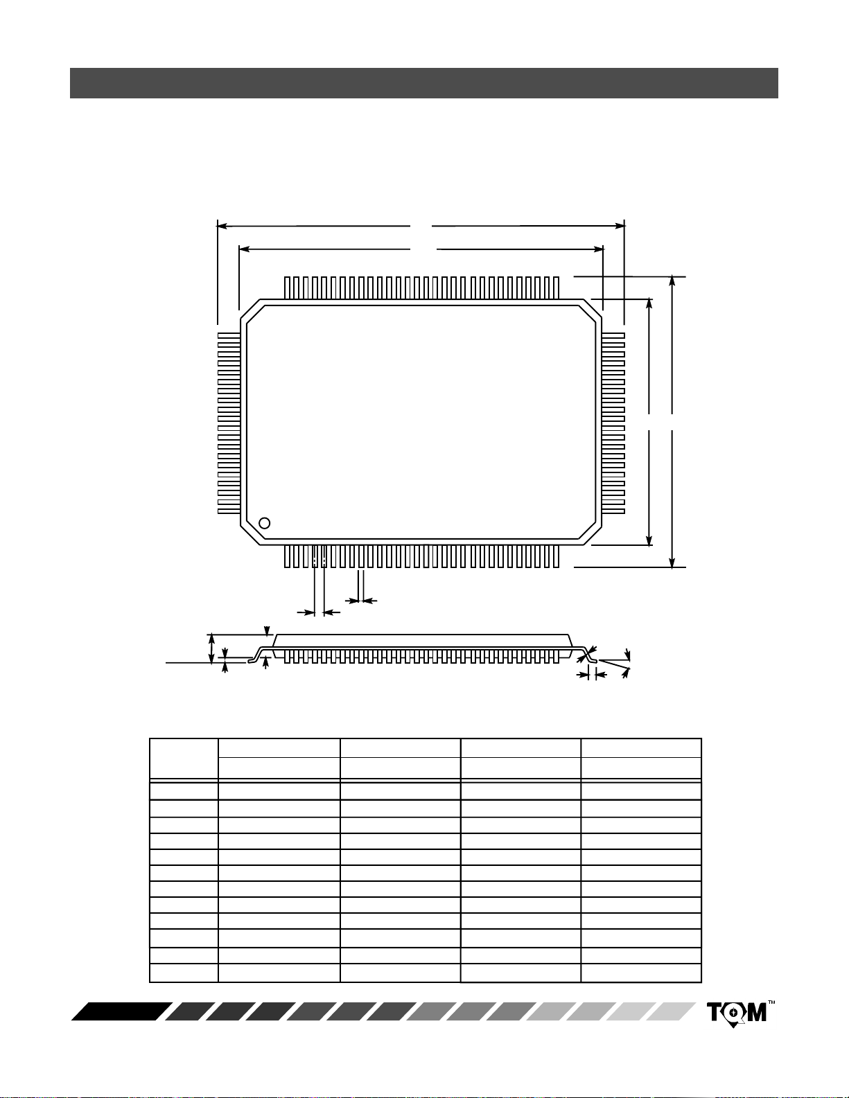
Package Dimensions
100 LEAD PLASTIC QUAD FLAT PACK
(14 mm x 20 mm, QFP)
Rev. 2.00
D
D
1
80 51
100
Seating Plane
81
130
A
2
A
B
e
50
E
E
1
31
C
α
A
1
L
1.6 mm Form 1.95 mm Form
INCHES MILLIMETERS
SYMBOL MIN MAX MIN MAX
A 0.102 0.130 2.60 3.30 0.102 0.134 2.60 3.40
A
1
A
2
B 0.009 0.015 0.22 0.38 0.009 0.015 0.22 0.38
C 0.005 0.009 0.13 0.23 0.005 0.009 0.13 0.23
D 0.904 0.923 22.95 23.45 0.931 0.951 23.65 24.15
D
1
E 0.667 0.687 16.95 17.45 0.695 0.715 17.65 18.15
E
1
e 0.0256 BSC 0.65 BSC 0.0256 BSC 0.65 BSC
L 0.029 0.040 0.73 1.03 0.026 0.037 0.65 0.95
0.002 0.010 0.05 0.25 0.002 0.014 0.05 0.35
0.100 0.120 2.55 3.05 0.100 0.120 2.55 3.05
0.783 0.791 19.90 20.10 0.783 0.791 19.90 20.10
0.547 0.555 13.90 14.10 0.547 0.555 13.90 14.10
INCHES MILLIMETERS
MIN MAX MIN MAX
α 0° 7° 0° 7° 0° 7° 0° 7°
Note: The control dimension is the millimeter column
Page 38
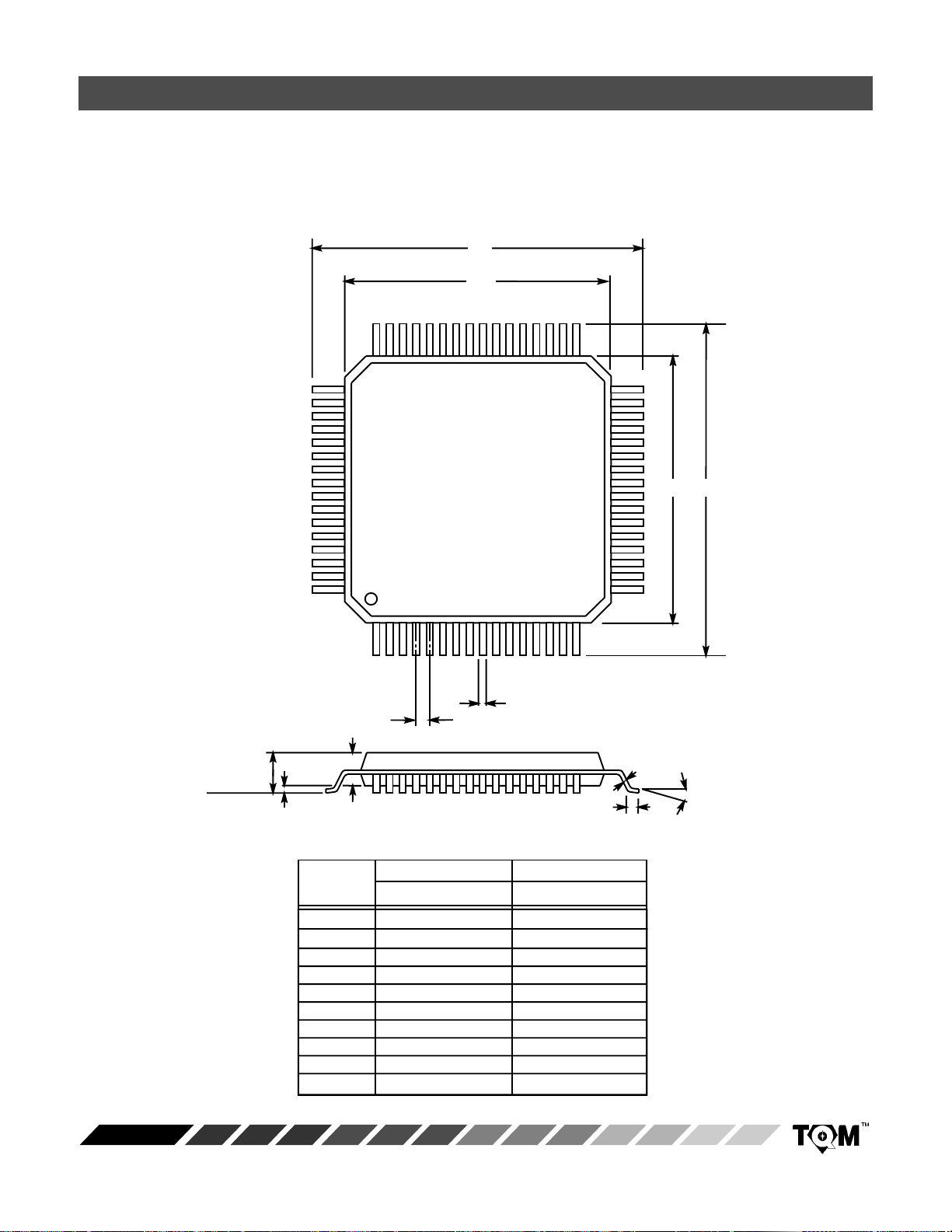
Package Dimensions
64 LEAD THIN QUAD FLAT PACK
(10 x 10 x 1.4 mm, TQFP)
Rev. 2.00
D
D
1
48 33
Seating Plane
49
64
116
A
2
A
e
B
32
D
D
1
17
C
α
A
1
L
INCHES MILLIMETERS
SYMBOL MIN MAX MIN MAX
A 0.055 0.063 1.40 1.60
A
1
A
2
B 0.005 0.009 0.13 0.23
C 0.004 0.008 0.09 0.20
D 0.465 0.480 11.80 12.20
D
1
e 0.020 BSC 0.50 BSC
L 0.018 0.030 0.45 0.75
0.002 0.006 0.05 0.15
0.053 0.057 1.35 1.45
0.390 0.398 9.90 10.10
α 0° 7° 0° 7°
Note: The control dimension is the millimeter column
Page 39
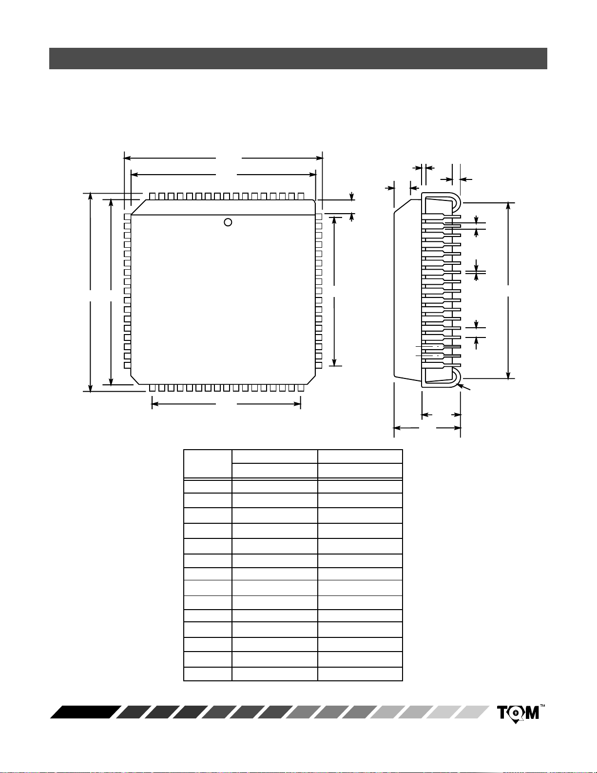
Package Dimensions
68 LEAD PLASTIC LEADED CHIP CARRIER
(PLCC)
Rev. 1.00
D D
D
D
1
1
268
1
D
3
45° x H2
D
3
45° x H1
C
A
A
1
Seating Plane
A
2
B
1
B
D
e
R
2
INCHES MILLIMETERS
SYMBOL MIN MAX MIN MAX
A 0.165 0.200 4.19 5.08
A
1
A
2
B 0.013 0.021 0.33 0.53
B
1
C 0.008 0.013 0.19 0.32
D 0.985 0.995 25.02 25.27
D
1
D
2
D
3
e 0.050 BSC 1.27 BSC
H1 0.042 0.056 1.07 1.42
H2 0.042 0.048 1.07 1.22
R 0.025 0.045 0.64 1.14
0.090 0.130 2.29 3.30
0.020 –––. 0.51 –––
0.026 0.032 0.66 0.81
0.950 0.958 24.13 24.33
0.890 0.930 22.61 23.62
0.800 typ. 20.32 typ.
Note: The control dimension is the inch column
Page 40

NOTICE
EXAR Corporation reserves the right to make changes to the products contained in this publication in order to improve design, performance or reliability . EXAR Corporation assumes no responsibility for the use of any circuits described herein, conveys no license under any patent or other right, and makes no representation that the circuits are
free of patent infringement. Charts and schedules contained here in are only for illustration purposes and may vary
depending upon a user’s specific application. While the information in this publication has been carefully checked;
no responsibility, however, is assumed for inaccuracies.
EXAR Corporation does not recommend the use of any of its products in life support applications where the failure or
malfunction of the product can reasonably be expected to cause failure of the life support system or to significantly
affect its safety or effectiveness. Products are not authorized for use in such applications unless EXAR Corporation
receives, in writing, assurances to its satisfaction that: (a) the risk of injury or damage has been minimized; (b) the
user assumes all such risks; (c) potential liability of EXAR Corporation is adequately protected under the circumstances.
Copyright 1994 EXAR Corporation
Reproduction, in part or whole, without the prior written consent of EXAR Corporation is prohibited.
 Loading...