Page 1

ST662A
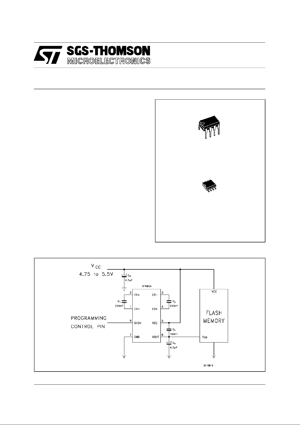
DC-DC CONVERTER FROM 5V TO 12V, 0.03A
FOR FLASH MEMORY PROGRAMMING SUPPLY
June 1997
■ OUTPUT VOLTAGE:12V± 5%
■ SUPPLYVOLTAGERANGE: 4.5V TO 5.5V
■ GUARANTEED OUTPUT CURRENT UPTO
30mA
■ VERYLOWQUIESCENTCURRENT: 100µA
■ LOGICCONTROLLEDELECTRONIC
SHUTDOWN: 1µA
■ JUSTCAPACITORSNEEDED(NO
INDUCTOR)
DESCRIPTION
The ST662A is a regulated charge pump DC-DC
converter.It provides12V ± 5% output voltage to
programbyte-wide flash memory, and can supply
30mA output current from inputas low as4.75V
A logic controlled shut down pin that interfaces
directly with microprocessor reduces the sypply
currentto only1µA
TYPICALAPPLICATION CIRCUIT
DIP-8
SO-8
1/12
Page 2

ABSOLUTE MAXIMUM RATINGS
Symbol Parameter Value Unit
V
cc
DC Input Voltage to GND -0.3 to 6 V
SHDN Shutdown Voltage -0.3 to V
CC
+0.3 V
I
o
OutputCurrent Continuous 50 mA
P
tot
Power Dissipation 500 mW
T
op
Operating Ambient Temperature Range(forAC SERIES)
(for AB SERIES)
0to70
-40to85
o
C
o
C
T
stg
StorageTemperature Range - 40 to 150
o
C
Absolute Maximum Rating are those values beyond which damage to the device may occur.
Functional operation under these condition is not implied.
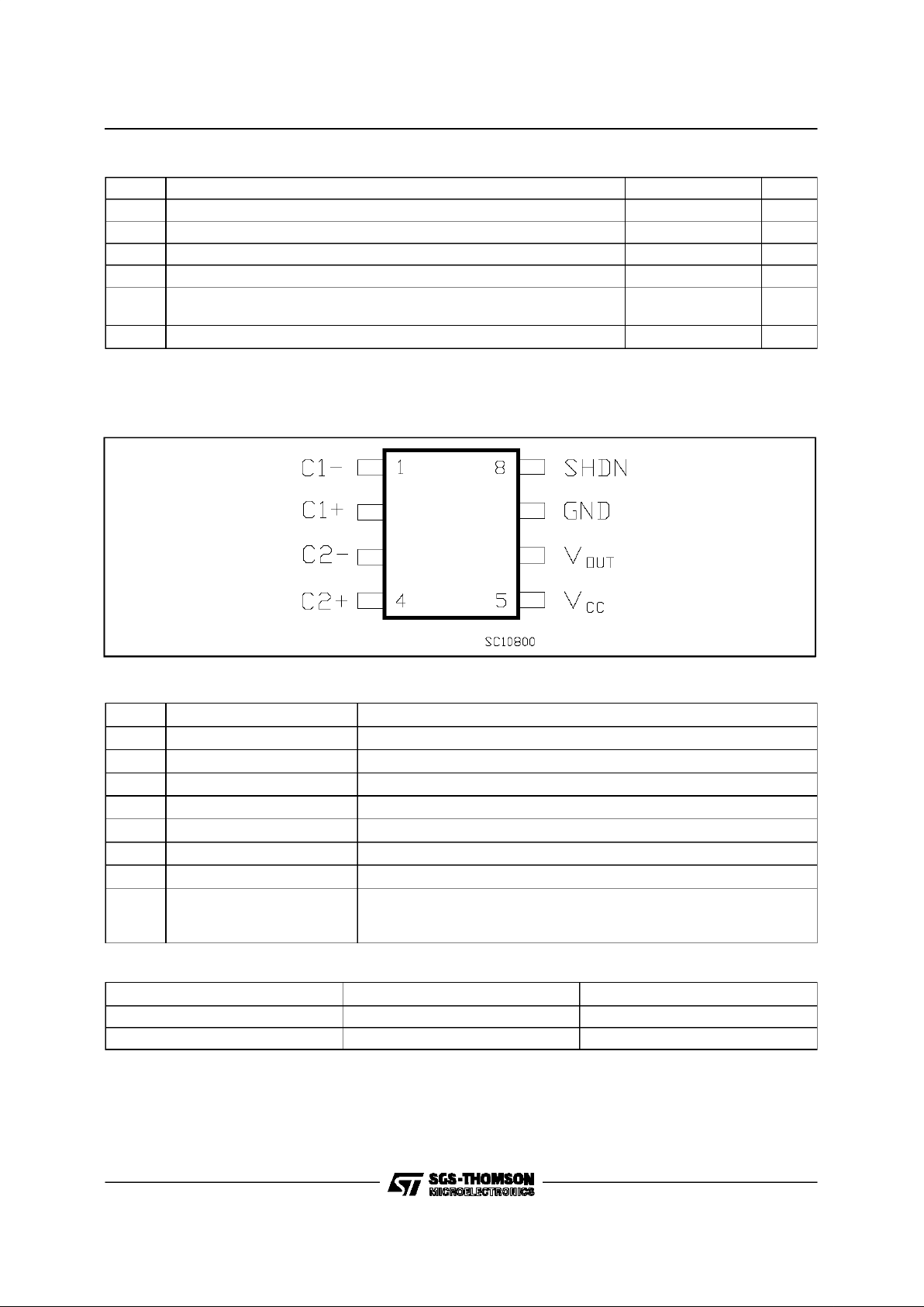
CONNECTION DIAGRAM AND (top view)
PINCONNECTIONS
Pin No Symbol Name and Function
1 C1- Negative Terminal For The FirstCharge Pump Capacitor
2 C1+ Positive Terminal For The FirstCharge Pump Capacitor
3 C2- Negative Terminal For The Second Charge Pump Capacitor
4 C2+ Positive Terminal For The SecondCharge Pump Capacitor
5V
CC
Supply Voltage
6V
OUT
12VOutputVoltage V
OUT=VCC
WheninSshutdownMode
7 GND Ground
8 SHDN ActiveHigh C-MOS logic level Shutdown Input. SHDNisinternally pulled up to
V
CC
. Connect to GND for NormalOperation. InShutdownmodethecharge
pumpsareturnedoff and V
OUT=VCC
ORDERING NUMBERS
Type DIP-8 SO-8 (*)
ST662AB ST662ABN ST662ABD
ST662AC ST662ACN ST662ACD
(*) AVAILABLE IN TAPE ANDREEL WITH ”-TR” SUFFIX
ST662A
2/12
Page 3

ELECTRICAL CHARACTERISTICS (Refer to the test circuits, VCC= 4.5V to 5.5V Ta=T
min
to T
max
unless otherwisespecified. TypicalValue are referred at Ta=25oC)
Symbol Parameter Test Conditions Min. Typ. Max. Unit
V
o
OutputVoltage Io= 0mA to20 mA 11.4 12 12.6 V
V
o
OutputVoltage Io= 0 mA to30mA VCC=4.75 to 5.5V 11.4 12 12.6 V
I
Q1
Quiescent Current No Load, V
SHDN
=0 100 500 µ A
I
Q2
Shutdown Current No Load, V
SHDN=VCC
110µA
I
SH
Shutdown Pin Current V
SHDN
=0V, VCC=5V
V
SHDN=VCC
=5V
-50 -12
0
-5 µA
µA
V
il
Shutdown Input LowThreshold 0.4 V
V
ih
Shutdown Input High
Threshold
2.4 V
f
o
OscillatorFrequency VCC= 5V, Io=30 mA 400 KHz
ν Power Efficecy V
CC
= 5V, Io=30mA 72 %
R
sw
VCC-V
OUT
Switch Impedance V
SHDN=VCC
=5V, Io=100µA12KΩ
Do not overload or short the Output to Ground. If the above conditions are observerd, the device may be damaged.
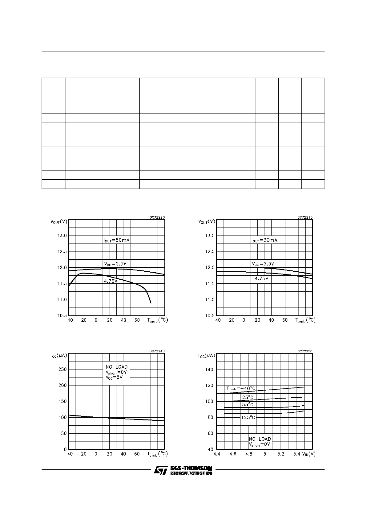
OutputVoltage vs Temperature
Supply Currentvs Temperature
OutputVoltage vs Temperature
SupplyCurrernt vs SupplyVoltage
ST662A
3/12
Page 4

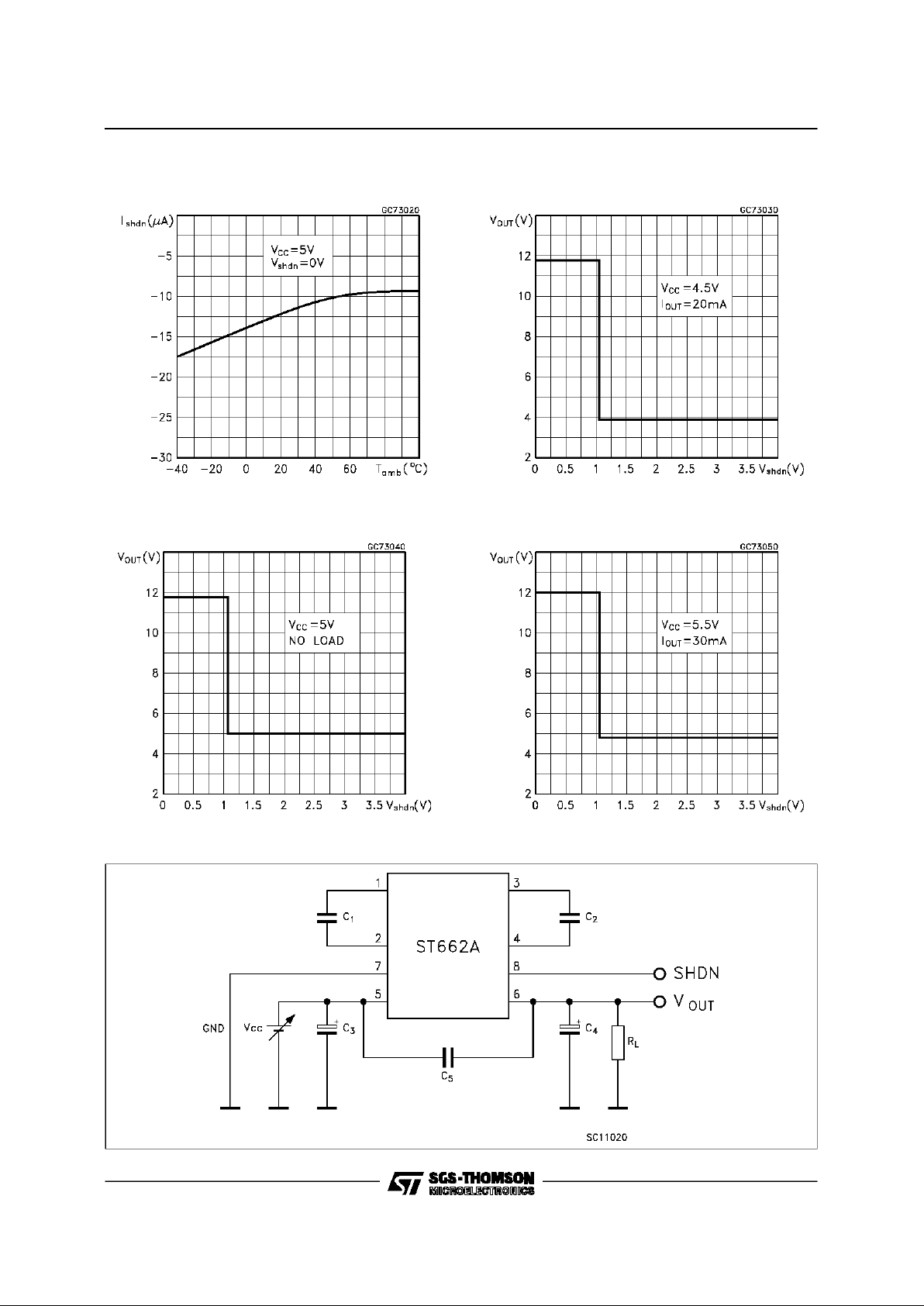
OutputVoltage vs Shutdown Input Voltage
Test Circuit
OutputVoltage vs Shutdown Input Voltage
SHDNPin Currentvs Temperature OutputVoltage vs Shutdown Input Voltage
ST662A
4/12
Page 5

DESCRIPTION
The ST662 is an IC developed to provide a 12V
regulated output 30mA from voltage input as low
as 4.75 without any inductors. It is useful for a
wide range of applications and its performances
makes it ideal for flash memory programming
supply.
An evaluation kit is provided to facilitate the
application. This include a single-side demo
board designed for surface-mount
components.The operating principle of ST662
(see fig. 1) is to charge C1 and C2 capacitor by
closing the S1 switch (while S2 is opened) at the
V
CC
voltage. After S1 will be opened and S2
closed so that C1 and C2 capacitors are placed
in series one to each other, and both are in series
with Vin.The sum of VC1 and VC2 and Vin is
applied to the capacitor C4. This works as
voltage tripler. An amplifier error checks the
output voltage and blocks the oscillator if the
output voltage is greaterthan12V.
The shutdown pin is internally pulled to V
CC
.
When it is held low the output voltage rises to
+12V. Fig.2 shows the transitiontime of the shut
down pin when the VSHDNgoes from 5V to 0V.
Input logic levels of this input are CMOS
compatible.
Applying a logic high at this input, the V
OUT
oscillator will be blocked and the V
OUT
will reach
theV
IN
value by D1. In this condition ICCwill be
Figure1: OperatingPrinciple Circuit
low as 1µA. The fig.3 shows the transition time
ofthe shut down pin when the VSHDNgoes from
0Vto 5V.
Figure2: Exiting Shutdown
TIME= 20us/DIV, VERTICAL = 5V/DIV
5V
0V
12V
5V
SHDN
Vout
Figure3: EnteringShutdown
TIME= 1ms/DIV, VERTICAL = 5V/DIV
5V
0V
12V
5V
SHDN
Vout
NOTE: VCC= 5V, I
OUT
= 200µA NOTE: VCC= 5V, I
OUT
=200µA
ST662A
5/12
Page 6

APPLICATIONCIRCUIT
Based on fast charge/discharge of capacitors,
this circuit involves high di/dt values limited only
by Ronof switches. This implies a critical layout
design due to the need to minimize inductive
paths and place capacitors as close as possible
to thedevice.
A good layout design is strongly recommended
for noise reason. For best performance, use very
short connections to the capacitors and the
valuesshown in table 1.
C3 and C4 must have low ESR in order to
minimize the output ripple. Their values can be
reduced to 2µF and 1µF, respectively, when
using ceramic capacitors, but mustbe of 10µFor
larger if aluminiumelectrolyticare chosen.
C5 must be placed as close to the device as
possible and could be omitted if very low output
noise performance are not required.
Fig 4 and Fig 5 show, respectively, our
EVALUATION kit layout and the relatively
electricalshematic.
Table 1: List of Components
CAPACITOR TYPE VALUE (µF)
Charge Pump C1 Cer amic 0.22
Charge Pump C2 Cer amic 0.22
Input C3 Elect r ol yt ic Tantalum 4.7
Out put C4 Elec t rol ytic Tant alum 4. 7
Decoupling C5 Ceramic 0. 1
Figure5: ElectricalSchematic
Figure4: KIT Lay-out
ST662A
6/12
Page 7

OutputVoltage vs Output Current
Load TransientResponse
TIME= 1ms/DIV
Iout
20mA/div
SHDN
Vout
Vout
100mV/div
Efficencyvs Output Current
Line Transient Response
TIME= 1ms/DIV
Vin
1V/div
Vout
200mV/div
5.5V
4.5V
ST662A OUTPUTPERFORMANCE
NOTE: VCC= 5V, I
OUT
= 0 to 30mA NOTE: VCC= 4.5 to 5.5V, I
OUT
= 30mA
ST662A
7/12
Page 8

Table 2: List of Components
CAPACITOR TYPE VALUE (µF)
C1A Ceramic 0.22
C2A Ceramic 0.22
C1B Ceramic 0.22
C2B Ceramic 0.22
C3 Elect r ol yt ic Tantalum 10
C4 Elect r ol yt ic Tantalum 10
C5 Ceramic 0.22
Figure6: ApplicationCircuit for TwoST662Ain Parallel
HOW TO INCREASE OUTPUT CURRENT OR
OUTPUTVOLTAGECAPABILITY
Current capability is limited by R
on
of internal
switches.It is possible to increaseit connectingin
parallel two or more ST662A devices; each one
of them cansupply 30mA. The figure 6 showsthe
electricschematic.The capacitors C3, C4 and C5
must be placed very close to the ICs on the
board. If this is not possible, you can place two
different capacitors, each of them of half value,
very close to the respective integrated circuit.
Fig. 8 show the Output Current capability of the
proposedcircuit.
If an output voltage greater than 12V is required,
it’s possible to realize the circuit of the following
diagram (figure 7). The relevant Output Current
capability is shown in figure 9 in which is shown
the output voltage vs load current.
ST662A
8/12
Page 9

Figure7: ApplicationCircuit for OutputVoltage greaterthan 12V
Figure8: OutputVoltage for the Applicationwith
Two Device in Parallel
Figure9: OutputVoltage forApplicationwith
OutputVoltage greater than12V
ST662A
9/12
Page 10

DIM.
mm inch
MIN. TYP. MAX. MIN. TYP. MAX.
A 3.3 0.130
a1 0.7 0.028
B 1.39 1.65 0.055 0.065
B1 0.91 1.04 0.036 0.041
b 0.5 0.020
b1 0.38 0.5 0.015 0.020
D 9.8 0.386
E 8.8 0.346
e 2.54 0.100
e3 7.62 0.300
e4 7.62 0.300
F 7.1 0.280
I 4.8 0.189
L 3.3 0.130
Z 0.44 1.6 0.017 0.063
P001F
Plastic DIP-8 MECHANICAL DATA
ST662A
10/12
Page 11

DIM.
mm inch
MIN. TYP. MAX. MIN. TYP. MAX.
A 1.75 0.068
a1 0.1 0.25 0.003 0.009
a2 1.65 0.064
a3 0.65 0.85 0.025 0.033
b 0.35 0.48 0.013 0.018
b1 0.19 0.25 0.007 0.010
C 0.25 0.5 0.010 0.019
c1 45 (typ.)
D 4.8 5.0 0.188 0.196
E 5.8 6.2 0.228 0.244
e 1.27 0.050
e3 3.81 0.150
F 3.8 4.0 0.14 0.157
L 0.4 1.27 0.015 0.050
M 0.6 0.023
S 8 (max.)
0016023
SO-8 MECHANICALDATA
ST662A
11/12
Page 12

Information furnished is believed to be accurateand reliable.However, SGS-THOMSONMicroelectronics assumes no responsabilityfor the
consequences of use of such informationnor for anyinfringement of patents or other rights ofthirdparties whichmay resultsfrom its use. No
licenseisgranted by implication or otherwise under anypatent orpatent rightsof SGS-THOMSON Microelectronics. Specifications mentioned
in this publicationare subject to change without notice.This publication supersedesandreplaces all informationpreviouslysupplied.
SGS-THOMSONMicroelectronicsproducts arenotauthorizedfor use ascritical components inlife support devicesorsystems withoutexpress
writtenapproval of SGS-THOMSON Microelectonics.
1997 SGS-THOMSONMicroelectronics- Printedin Italy- All Rights Reserved
SGS-THOMSONMicroelectronics GROUPOF COMPANIES
Australia- Brazil - Canada- China- France - Germany-Hong Kong - Italy-Japan - Korea - Malaysia - Malta - Morocco- The Netherlands-
Singapore- Spain- Sweden - Switzerland- Taiwan - Thailand - United Kingdom- U.S.A
.
ST662A
12/12
 Loading...