

Datasheet ST63T73J5B1, ST6373, ST63E73J5D1, ST6373J5B1, ST6373J3B1 Datasheet (SGS Thomson Microelectronics)
...Page 1
R
ST6373
8-BIT ROM/OTP/EPROM MCUs FOR DIGITALLY
CONTROLLED MULTISYNC/MULTISTANDARD MONITORS
■ 4.5V to 6V Operating Supply Voltage Range
■ Low Current Consumption
■
0to+70°C Operating Temperature Range
■
8 MHzclock Oscillator
■ 16K bytes ROM/OTP/EPROM
(8K and 12K ROM versions also available)
■
192 bytes RAM
■ 384 bytes general purpose EEPROM
■ 128 bytes dedicated EEPROM for DDC SPI
■ 22 fully programmable I/O pins, offering direct
LED drive capability, as well as interrupt
generation for keyboard inputs
■ Digital WATCHDOG timer
■ Three Timers, each comprising an 8-bit counter
and a 7- bit Prescaler
■ SYNC Processor:
– 12-bits HSYNC Event Counter
– 12-bits VSYNC Period Counter
– HSYNC and VSYNC Polarity Detection
– HSYNC and VSYNC Outputs
– HFLYBACK and VFLYBACK Inputs
– CLAMP and BLANK Outputs
■ 14-bit (PWM + BRM) D/A Converter
■ Nine 7-bit PWM D/A Converter Outputs
■
8-bit A/D Converter with 8 multiplexed inputs
■ DDC SPI with interrupt and 4 operating modes
■ A further SPI with interrupt and 2 operating
modes
■
Remote Control Signal Input (Non Maskable
Interrupt)
■ VSYNC Interrupt Input
■ Five Interrupt Vectors
■
XOR Register (Instruction Set expansion)
■ MIRROR Register (Instruction Set expansion)
(Refer to end of Document for Ordering Information)
PSDIP42
CSDIP42
February 1998 1/64
ThisisadvanceinformationfromSGS-THOMSON.Detailsaresubject tochangewithoutnotice.
1
Page 2

Table of Contents
ST6373 . . . . . . . . . . . . . . . . . . . . . . . . . . . . . . . . . . . . . . . . . . . . .1
1 GENERAL DESCRIPTION . . ....................................................4
1.1 INTRODUCTION . . . . . . . ..................................................4
1.2 PIN DESCRIPTION . . . . . . . ................................................6
1.3 MEMORY SPACES .......................................................8
1.3.1 Stack Space . . . . . . . . . . ..............................................8
1.3.2 Program Space . .. . . ................................................8
1.3.3 Data Space .......................................................10
1.3.4 Data RAM/EEPROM ................................................12
1.3.5 EEPROM Description . . . . . . . . . . . . . ..................................12
1.4 MEMORYPROGRAMMING ...............................................15
1.4.1 Program Memory . . . . . . . . . ..........................................15
1.4.2 Option Byte .......................................................15
1.4.3 Eprom Erasure . . . . . . . ..............................................15
2 CENTRAL PROCESSING UNIT . . . ..............................................16
2.1 INTRODUCTION . . . . . . . .................................................16
2.2 CPU REGISTERS .......................................................16
3 CLOCKS, RESET, INTERRUPTS AND POWER SAVING MODES .....................18
3.1 ON-CHIP CLOCK OSCILLATOR. . . . . . . . . . . . . . . . . . . . . . . . . . . . ................18
3.2 RESETS...............................................................19
3.2.1 RESET Input . . . . . . . ...............................................19
3.2.2 Power-on Reset . . . . . . . . . . . . . . . .....................................19
3.2.3 Watchdog Reset . ..................................................20
3.2.4 Application Note . . . . . . . . . . . . . . . .....................................20
3.2.5 MCU Initialization Sequence ..........................................20
3.3 HARDWARE ACTIVATED DIGITAL WATCHDOG FUNCTION . .. . . ...............21
3.4 INTERRUPT . . . . . . . . . . .. . . . .. . . .........................................23
3.4.1 Interrupt Vectors/Sources . ...........................................23
3.4.2 Interrupt Priority . . . . . . . . . . . . . . . .....................................24
3.4.3 Interrupt Option Register . . . . . . . . . . . . . . . . . . . . . ........................24
3.4.4 Interrupt Procedure .................................................25
3.4.5 ST6373 Interrupt Details . . . . . . . . . . . . . . . . . . . . . ........................25
3.5 POWER SAVING MODES. . . ..............................................28
3.5.1 WAIT Mode .......................................................28
3.5.2 STOP Mode . . . . . . . . . . . ............................................28
3.5.3 Exit from WAIT Mode . . . . . . . .........................................28
4 ON-CHIP PERIPHERALS ......................................................29
4.1 I/OPORTS.............................................................29
4.1.1 Details of I/O Ports A and B . . . . . . . . . . . . . . . . . . .........................30
4.1.2 Details of I/O Port C . . . ..............................................31
4.1.3 I/O Port Registers ..................................................34
4.2 TIMERS ...............................................................35
4.2.1 Timer Operating Modes . . . . ..........................................36
4.2.2 Timer StatusControl Registers (TSCR). . . ...............................37
4.2.3 Timer Counter Registers (TCR) . . . . . . . . . . . . . . .. . . . .....................37
64
2/64
Page 3

Table of Contents
4.2.4 Timer Prescaler Registers (PSC). . .....................................37
4.3 A/D CONVERTER (ADC) . . . . . . . . ..........................................38
4.3.1 Application Notes . . . . . . . . . ..........................................38
4.4 SYNC PROCESSOR . . . . . . . ..............................................40
4.4.1 Event Counter . . ...................................................40
4.4.2 Period Counter . . . . . . . ..............................................40
4.4.3 Polarity Detector . ..................................................40
4.4.4 Output Polarity Control ...............................................40
4.4.5 Video Blanking Generator . ...........................................41
4.5 14-BIT PWM D/A CONVERTER ............................................44
4.5.1 Output Details . . ...................................................44
4.5.2 HDA Tuning Cell Registers ...........................................44
4.6 7-BIT PWM D/A CONVERTERS ............................................45
4.6.1 Digital Outputs . . . . . . . ..............................................45
4.7 SERIAL PERIPHERAL INTERFACES. . . . . . . . . . . . . . . . . . . .....................46
4.7.1 SPI Modes ........................................................47
4.8 MIRROR REGISTER . . . . . . . ..............................................51
4.9 XOR REGISTER . . . . . . . .................................................51
5 SOFTWARE . . . . . . . . . .......................................................52
5.1 ST6 ARCHITECTURE . . . . . . . . . . . . . . . .....................................52
5.2 ADDRESSING MODES . . . . . . . . ...........................................52
5.3 INSTRUCTION SET ......................................................53
6 ELECTRICAL CHARACTERISTICS. . . . ..........................................58
6.1 ABSOLUTE MAXIMUM RATINGS. . . . . . . . . . . . . . . . . . .........................58
6.2 RECOMMENDED OPERATING CONDITIONS. . . . .............................58
6.3 DC ELECTRICAL CHARACTERISTICS . . ....................................59
6.4 AC ELECTRICAL CHARACTERISTICS . .....................................60
7 GENERAL INFORMATION . . . . . . . ..............................................61
7.1 PACKAGE MECHANICAL DATA. . . . . . . . .. . . . . . . . . . . . . . . . . . . ................61
7.2 ORDERING INFORMATION . . . . . . . . .. . . . ..................................62
3/64
1
Page 4

ST6373
1 GENERAL DESCRIPTION
1.1 INTRODUCTION
ST6373 Microcontrollers are members of the 8-bit
HCMOS ST637x family, a series of devices specially intended for Digitally Controlled Multi Frequency Monitor applications. All ST637x devices
are based on a building block approach: a common core is surrounded by a combination of onchip peripherals (macrocells) available from a
standard library.
ST6373 devices are available in functionally identical ROM, OTP (ST63T73) and EPROM
(ST63E73) versions, all with the same pinout.
ROM devices are available with 8, 12 or 16K Program memory, whereas OTP and EPROM versions are both available in 16K versions only. For
details relating to sales types, refer to Section 7.2.
Since ROM, OTP and EPROM versions are
functionally identical, the present Datasheet
will refer to the generic ST6373 device, except
where specific versions differ in detail.
The ST6373 devices feature:
– Nine PWM outputs, which can be used as Digital
to Analog converter outputs (withexternal RC filters). These are suitable for tuning and other
functions.
– A PWM output with Bit Rate Multiplier, to which
the above comments apply.
– An Event Counter especially designed to calcu-
late the HSYNC (or HDRIV) Frequency, using
one of the on-chip timers.
– A Period Counter especially designed to calcu-
late the VSYNC Period.
– A Polarity Detector for HSYNC (or HDRIV) and
VSYNC.
– HSYNC and VSYNC outputs with controlled po-
larity.
– Video Blanking and Clamping Outputs.
– Two I/O ports A & B usable for a keyboard wake-
up feature since an interrupt input ored on each
of their pins.
– An Analog to Digital converter connected to port
B which can be used to decode an analog key-
board or for AFC.
– A VSYNC input pin connected to an interrupt
vector and to the DDC SPI for DDC1 protocol.
– An NMI inputwhich canbe used, forexample, as
a Remote Control input for a TV application.
– A hardware DDC SPI able to manage DDC1
(VSYNC as clock), DDC2B and DDC2AB (I2C
BUS Multimaster and Slave). A 128-byte
dedicated EEPROM memory is available for
DDC1 and DDC2B.
– Hardware I2C SPI for internal monitor bus and to
manage, for example, an OSD.
– A Mirror Register and a XOR Register are includ-
ed to complement the basic ST6 instruction set.
Table 1. ST6373 Device Summary
DEVICE
CONFIGURATION
ST6373
ST63T73 16K OTP 192 512 8 1 9 ST63E73 16K EPROM 192 512 8 1 9 -
Note: See
4/64
Ordering Information in Table 23 at the end of the Datasheet.
Program
Memory
(Bytes)
8K ROM
12K ROM
16K ROM
RAM
(Bytes)
192 512 8 1 9 ST63E73,ST63T73
EEPROM
(Bytes)
A/D
Inputs
14-bit
D/ (PWM)
Output
7-bit
D/A (PWM)
Output
EMULATING
DEVICES
Page 5
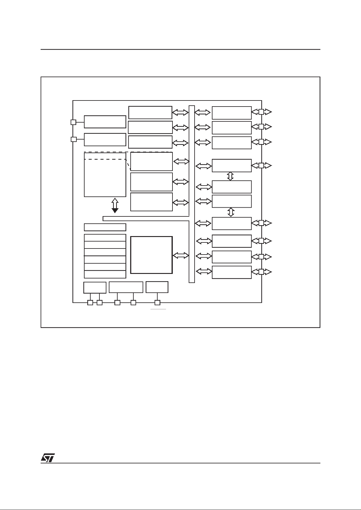
Figure 1. ST6373 Block Diagram
ST6373
TEST/V
(**)
PP
NMI
VSYNC
PWRIN
TEST
INTERRUPT
Inputs
USER PROGRAM
MEMORY
16 KBytes
PC
STACK LEVEL1
STACK LEVEL2
STACK LEVEL3
STACK LEVEL4
STACK LEVEL5
STACK LEVEL6
POWER
SUPPLY
OSCILLATOR
TIMER 1
TIMER 2
DIGITAL
WATCHDOG/TIMER
DATA ROM
USER
SELECTABLE
DATARAM
192 Bytes
DATA EEPROM
384 Bytes
8 BIT CORE
RESET
PORT A
PORT B
PORT C
DDC SPI (1)
EEPROM
128 Bytes (1)
TIMER 3
SYNC
PROCESSOR
I C SPI
D/A Outputs
A/D Inputs
PA0 -> PA7*
PB0 -> PB7*
PC0 -> PC7*
SCLD, SDAD
VSY NC, EXTCLK
HSYNC O, VSYNCO
HSYNC I, VSYNCI
HDRIV
HFLY, VFL Y
CLMPO, BLK O
SCLI, SDAI
HDA, DA0 -> DA8
AD0 -> AD7
V
DDVSS
OSCin OSCout RESET
(*)Refer to Pin Description for Add itional Information
(**)VPPinput for OTP/EPROM deviceprogramming
5/64
Page 6
ST6373
1.2 PIN DESCRIPTION
VDDand V
these two pins. VDDis power and VSSis the
Power is supplied to the MCU using
SS.
ground connection.
OSCin, OSCout.
These pins are internally connected to the on-chip oscillator circuit. A quartz
crystal or a ceramic resonator can be connected
between these two pins in order to allow the correct operation of the MCU with various stability/cost trade-offs. The OSCin pin is the input pin,
the OSCout pin is the output pin.
RESET. The active lowRESETpin is used to start
the microcontroller to the beginning of its program.
Additionally the quartz crystal oscillator will be disabled when theRESET pin is low toreduce power
consumption during reset phase.
TEST
. The TEST pin mustbe held at VSS for nor-
mal operation.
PA0, PA1, PA2/HSYNCO, PA3/VSYNCO,
PA4/CLMPO, PA5/BLKO, PA6/SCLI, PA7/SDAI
Port A.
–
Software configurable as push-pull output, open-drain output, Schmitt trigger input with
or without pull-up. Port A inputs can be also
ORed into the INT1 interrupt. Port A outputs
have a LED drive capability (10 mA). Pins PA2
and PA3 can be configured respectively as
HSYNC and VSYNC outputs.Pins PA4 and PA5
can be configured respectively as CLAMP and
BLANK Outputs.Pins PA6 and PA7 can be configurated as the I2C SPI pins SCLI and SDAI.The
push-pull output and the input pull-up options do
not exist for these two pins. After reset the PA0
to PA5 pins are configured as inputs with pull-up.
PB0/AD0, PB1/AD1, PB2/AD2, PB3/AD3,
PB4/AD4, PB5/AD5/HFLY, PB6/AD6/VFLY,
PB7/AD7
Port B
–
. Each pin can be software configured as
push-pull output, open-drain output, Schmitt trigger inputwith or without pull-up.Port B inputs can
be also ored into the INT1 interrupt. Pins PB5
and PB6 can be configured as HFLY and VFLY
inputs. In addition, any pin of port B can be software selected as the Analog-to-Digital converter
input. Only one pin should be selected at a time,
otherwise a conflict would result. After reset the
port B pins are configured as inputs with pull-up.
PC0/SCLD, PC1/SDAD, PC2, PC3/EXTCLK,
PC4/PWRIN, PC5, PC6/HSYNC, PC7/HDRIV
– Port C. Software configurable as open-drain out-
puts or Schmitt trigger inputs with or without pullups. When configured as outputs, pins PC0 to
PC3 are configured as 5V open-drain. Pins PC4
to PC7 are configured as open-drain 12V; the input pull-up option does not exist for these four
pins. Pins PC0, PC1 and PC3 can be configured
as the DDCSPI pins SCLD, SDADand EXTCLK.
The input pull-up option does not exist for PC0
and PC1. Pins PC6 and PC7 can be configured
as HSYNC and HDRIV inputs.After reset: PC3 is
configured as input with pull-up. PC0, PC1 &
PC4 to PC7 are configured in input without pullup. PC2 is in output mode with the value 1 (high
impedance).
DA0-DA8. These pins are the nine PWM D/A outputs of the on-chip D/A converters. These lines
have push-pull outputs with 5V drive. The output
repetition rate is 31.25KHz (with 8MHz clock).
VSYNC. This is the Vertical Synchronization pin.
This pin is connected to an internal interrupt and is
configured as input with pull-up and Schmitt trigger.
HDA. This is the output pin of the on-chip 14-bit
PWM D/A Converter. This line is a push-pull output with standard drive.
NMI
. This pin is the Non-Maskable interrupt input
and is configured as input withpull-up and Schmitt
trigger.
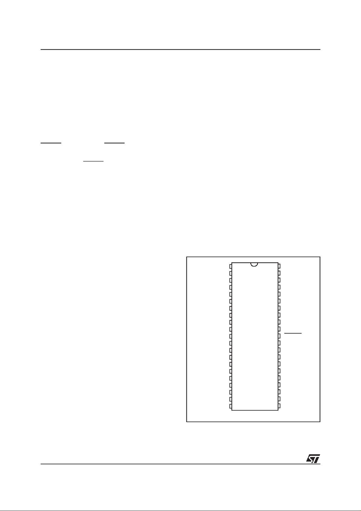
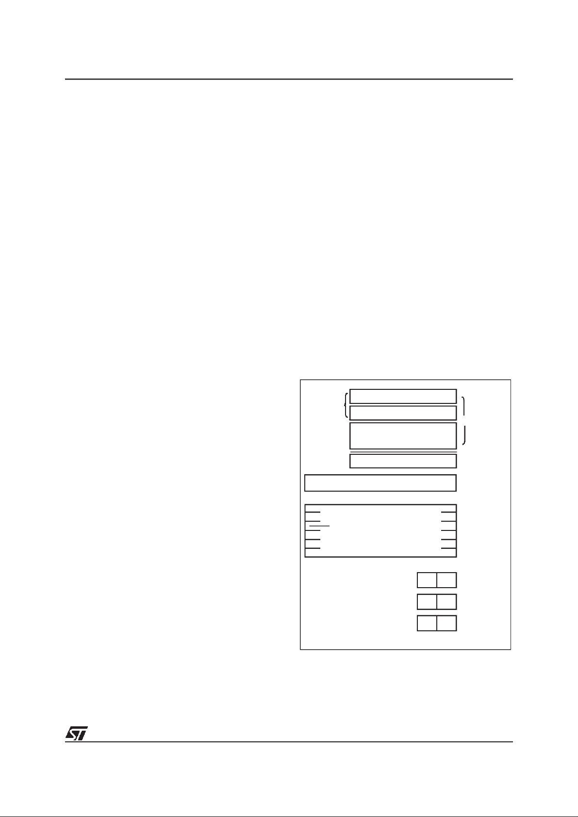
Figure 2. ST6373 Pin configuration
V
DD
O0/DA0
O1/DA1
O2/DA2
O3/DA3
AD0/PB0
AD1/PB1
AD2/PB2
AD3/PB3
AD4/PB4
HFLY/AD5/PB5
VFLY/AD6/PB6
AD7/PB7
PA0
PA1
HSYNCO/PA2
VSYNCO/PA3
CLMPO/PA4
BLKO/PA5
SCLI/PA6
SDAI/PA7
(1) This pin is also the VPPinput for OTP/EPROM devices
1
2
3
4
5
6
7
8
9
10
11
12
13
14
15
16
17
18
19
20
V
SS
21
42
PC0/SCLD
41
PC1/SDAD
40
PC2
39
PC3/EXTCLK
38
PC4/PWRIN
37
PC5
36
PC6/HSYNC
35
PC7/HDRIV
34
HDA
33
RESET
32
OSCout
31
OSCin
30
TEST/V
29
28
VSYNC
27
NMI
26
DA4/O4
25
DAR/O5
24
DA6/O6
23
DA7/O7
22
DA8/O8
PP
(1)
6/64
Page 7

Table 2. Pin Summary
Pin Function Description
DA0 to DA8 Output, Push-Pull
HDA Output, Push-Pull
NMI Input, Pull-up, Schmitt Trigger Input
VSYNC Input, Pull-up, Schmitt Trigger
TEST Input, Pull-Down
OSCin Input, Resistive Bias, SchmittTrigger to Reset Logic Only
OSCout Output, Push-Pull
RESET Input, Pull-up, Schmitt Trigger Input
PA0-PA5 I/O, Push-Pull/Open Drain, Software Input Pull-up, Schmitt Trigger Input
PA6-PA7 I/O, Open-Drain, No Input Pull-up, Schmitt Trigger Input
PB0-PB7 I/O, Push-Pull/Open Drain, Software Input Pull-up, Schmitt Trigger Input, Analog Input
PC0-PC1 I/O, Open-Drain, No Input Pull-up, Schmitt Trigger Input
PC2-PC3 I/O, Open-Drain, 5V, Software Input Pull-up, Schmitt Trigger Input
PC4-PC7 I/O, Open-Drain, 12V, No Input Pull-up, Schmitt Trigger Input
V
DD,VSS
Power Supply Pins
ST6373
7/64
Page 8
ST6373
1.3 MEMORY SPACES
The MCU operates in three different memory
spaces: Stack Space, Program Space and Data
Space.
1.3.1 Stack Space
The stackspace consists of six 12bit registers that
are used for stacking subroutine and interrupt return addresses plus the current program counter
register.
1.3.2 Program Space
The program space is physically implemented in
the ROM and includes all the instructions that are
to be executed, as well as the data required for the
immediate addressing mode instructions, the reserved test area and user vectors. It is addressed
thanks to the 12-bit Program Counter register (PC
register) and theST6 Corecan directly address up
to 4K bytes of Program Space. Nevertheless, the
Program Space can be extended by the addition
of 2-Kbyte memory banks as it is shown inFigure
2, in which the 16K bytes memory is described.
These banks are addressed by pointing to the
000h-7FFh locations of the Program Space thanks
to the Program Counter, and by writing the appropriate code in the Program ROM Page Register
(PRPR) located at address CAh in the Data
Space. Because interrupts and common subrouroutines should be available all the time only the
Figure 4. Memory Addressing Diagram
lower 2K byte of the 4K program space are bank
switched while the upper 2K byte can be seen as
static space. Table 3 gives the different codesthat
allows the selection of the corresponding banks.
Note that,from thememory point ofview, the Page
1 and the Static Page represent the same physical
memory: it is only a different way ofaddressing the
same location.
Figure 3.16K-Byte Program Space Addressing
Program
counter
space
0FFFh
0800h
07FFh
0000h
0000h
Static
Page
Page 1
Page 0
Page1
Static
Page
Page
Page Page Page Page Page
2345 67
1FFFh
PROGRAM COUNTER
STACK LEVEL 1
STACK LEVEL 2
STACK LEVEL 3
STACK LEVEL 4
STACK LEVEL 5
STACK LEVEL 6
0000h
0FF0h
RESET VECTORS
0FFFh
PROGRAM SPACE
ROM
INTERRUPT&
0-63
000h
03Fh
040h
07Fh
080h
081h
082h
083h
084h
0C0h
0FFh
DATA SPACE
RAM / EEPROM
BANKING AREA
DATA ROM
WINDOW
X REGISTER
Y REGISTER
V REGISTER
W REGISTER
RAM
DATA ROM
WINDOW SELECT
DATA RAM
BANK SELECT
ACCUMULATOR
8/64
Page 9
MEMORY SPACES (Cont’d)
Program ROM Page Register (PRPR)
Address: CAh - Write only
Reset Value: XXh
70
- - - - - PRPR2 PRPR1 PRPR0
Care is required when handling the PRPR as it is
write only. For this reason, it is not allowed to
change the PRPR contents while executing interrupts drivers, asthe driver cannotsaveand thanrestore its previous content. Anyway, this operation
may be necessary if the sum of common routines
and interrupt drivers will take more than 2K bytes;
in this case could be necessary to divide theinterrupt driver in a (minor) partin the static page (start
D7-D3. These bits are not used but have to be
written to “0”.
PRPR2-PRPR0.
These are the program ROM
banking bits and the value loaded selects the corresponding page to be addressed in the lower part
of 4Kprogram address space as specified inTable
3.This register is undefined on reset.
Note:
Only the lower part of address space has been
bankswitched because interrupt vectors and common subroutines should be available all the time.
The reason of this structure is due to the fact that it
is not possible to jump from a dynamic page to another, unless jumping back to the static page,
changing contents of PRPR, and, then, jumping to
a different dynamic page.
and end), and in thesecond (major) part in one dynamic page.Ifitis impossible to avoid the writingof
this register in interrupts drivers, an image of this
register mustbesavedina RAM location, andeach
time the program writes the PRPR bit writes also
the image register. The image register must be
written first, so if an interrupt occurs between the
two instructions the PRPR is not affected.
Table 3.ProgramMemoryPageRegisterCoding
PRPR2 PRPR1 PRPR0 PC11 Memory Page
X X X 1 Static Page (Page 1)
0000Page0
0 0 1 0 Page 1 (Static Page)
0100Page2
0110Page3
1000Page4
1010Page5
1100Page6
1110Page7
ST6373
Table 4. ST6373 Program Memory Map
Program Memory Page Device Address Description
PAGE 0
PAGE 1
“STATIC”
PAGE 2
PAGE 3
PAGE 4
PAGE 5
PAGE 6
PAGE 7
0000h-007Fh
0080h-07FFh
0800h-0F9Fh
0FA0h-0FEFh
0FF0h-0FF7h
0FF8h-0FFBh
0FFCh-0FFDh
0FFEh-0FFFh
0000h-000Fh
0010h-07FFh
0000h-000Fh
0010h-07FFh
0000h-000Fh
0010h-07FFh
0000h-000Fh
0010h-07FFh
0000h-000Fh
0010h-07FFh
0000h-000Fh
0010h-07FFh
User ROM (End of 12K)
User ROM (End of 16K)
Note*): all reserved areas must be set to FFh in the ROM code.
*)
Reserved
User ROM
User ROM
Reserved
Interrupt Vectors
Reserved
NMI Vector
Reset Vector
Reserved
User ROM
Reserved
User ROM (End of 8K)
Reserved
User ROM
Reserved
Reserved
User ROM
Reserved
9/64
Page 10

ST6373
MEMORY SPACES (Cont’d)
1.3.3 Data Space
The ST6 Coreinstruction set operates on a specific space, referred to as the Data Space, which
contains all the data necessary for the program.
Figure 5. Data Space
DATA RAM/EEPROM
BANK AREA
DATA ROM
WINDOWAREA
X REGISTER 080h
Y REGISTER 081h
V REGISTER 082h
W REGISTER 083h
DATA RAM
PORT A DATA REGISTER 0C0h
PORT B DATA REGISTER 0C1h
PORT C DATA REGISTER 0C2h
RESERVED 0C3h
PORT A DIRECTIONREGISTER 0C4h
PORT B DIRECTIONREGISTER 0C5h
PORT C DIRECTION REGISTER 0C6h
RESERVED 0C7h
INTERRUPT OPTIONREGISTER 0C8h
DATA ROM WINDOW REGISTER 0C9h
PROGRAM ROM PAGEREGISTER 0CAh
I C SPI DATA REGISTER 0CBh
DDC SPI DATA REGISTE R 0CCh
PORT A OPTION REGISTER 0CDh
PORT B OPTION REGISTER 0CEh
RESERVED 0CFh
ADC RE SULT REGISTER 0D0h
ADC CONTROL REGISTER 0D1h
TIMER 1 PRESCALERR EGISTER 0D2h
TIMER 1 COUNTER REGISTER 0D3h
TIMER 1 STATUS/CONTROL REGISTER 0D4h
TIMER 2 PRESCALERR EGISTER 0D5h
TIMER 2 COUNTER REGISTER 0D7h
WATCHDOG REGISTER 0D8h
000h
03Fh
040h
07Fh
084h
0BFh
*)
*)
The Data Space allows the addressing of RAM
(192 bytes), EEPROM (384 bytes plus 128 bytes
for the DDC SPI), ST6 Core and peripheral registers, as well as read-only data such as constants
and look-up tables.
MIRROR REGISTER 0D9h
TIMER 3 PRESCALERREGISTER 0DAh
TIMER 3 COUNTER REGISTER 0DBh
TIMER 3 STATUS/CONTROL REGISTER 0DCh
EVE NT COUNTER DATA REGISTER 1 0DDh
EVE NT COUNTER DATA REGISTER 2 0DEh
SYNC PROCESSOR CONTROL REGISTE R 0DFh
D/A 0/4 DATA CONTROL REGISTER 0E0h
D/A 1/5 DATA CONTROL REGISTER 0E1h
D/A 2/6 DATA CONTROL REGISTER 0E2h
D/A 3/7 DATA CONTROL REGISTER 0E3h
D/A 8 DATA CONTROL REGISTER 0E4h
I C SPI CONTROL REGISTE R 1 0E5h
I C SPI CONTROL REGISTE R 2 0E6h
D/A BA NK REGISTER 0E7h
DATA RAM BANK REGISTER 0E8h
DDC EEPROM CONTROL REGISTER 0E9h
EEPROM CO NTROL R EGISTER 0EAh
DDC SPI CONTROL REGISTER 1 0EBh
DDC SPI CONTROL REGISTER 2 0ECh
NMI/PWRIN/VSYNC INTERRU PT REGISTER 0EDh
HDA DATA REGISTER 1 0EEh
HDA DATA REGISTER 2 0EFh
PERIOD COUNTER DATA REGISTER 0F0h
PERIOD COUNTER 1 AND BLANK CTRLREG. 0F1h
AUTO-COU NTER REGISTER 0F2h
SCL LATCHAND DDC2B ADDRESSCTRL REG. 0F3h
XOR REGISTER 0F4h
RESERVED
ACCUMULATOR 0FFh
*)
*)
*)
*)
*)
*)
*)
*)
*)
*)
*)
*)
*)
0F5h
0FEh
*) These registers contain write only bits, in which
case the bit operation instructions are not possible.
10/64
Page 11
MEMORY SPACES (Cont’d)
Data ROM Addressing.All the read-only data are
physically implemented in the ROM in which the
Program Space is also implemented. The ROM
therefore contains theprogram tobe executedand
also the constants and the look-up tables needed
for the program. The locations of Data Space in
which the different constants and look-up tables
are addressed by the ST6 Core can be considered
as being a 64-byte window through which it is possible to access to the read-only data stored in the
ROM. This window is located from the 40h address to the 7Fh address in the Dataspace and allows the direct reading of the bytes from the 000h
address to the 03Fh address in the ROM. All the
bytes of the ROM can be used to store either instructions or read-only data. Indeed, the window
can be moved by step of 64 bytes along the ROM
in writing the appropriate code in the Write-only
Data ROM Window register (DRWR, location
C9h). The effective address of the byte to be read
as a data in the ROM is obtained by the concatenation ofthe 6 less significant bits of the address in
the Data Space (as less significant bits) and the
content of the DRWR (as most significant bits). So
when addressing location 40h of data space, and
0 is loaded in the DRWR, the physical addressed
location in ROM is 00h.
Figure 6. Data ROM Window Memory Addressing
ST6373
Data ROM Window Register (DWR)
Address: C9h - Write only
Reset Value: XXh
70
DWR7 DWR6 DWR5 DWR4 DWR3 DWR2 DWR1 DWR0
DWR7-DWR0. These are the Data Rom Window
bits that correspond to the upper bits of data ROM
program space. Thisregister is undefined after reset.
Note:
Care is required when handling the DRWR as it is
write only. For this reason, it is not allowed to
change the DRWR contents while executing interrupts drivers, as the driver cannot save and than
restore its previous content. If it is impossible to
avoid the writing of this register in interrupts drivers, an image of this register must be saved in a
RAM location, and each time the program writes
the DRWR it writes also the image register. The
image register must be written first, so if an interrupt occurs between the two instructions the
DRWR register is not affected.
DATA ROM
WINDOW REGISTER
CONTENTS
(DWR)
Example:
DWR=28h
ROM
ADDRESS:A19h
13
12
7
65432 0
0
0
00000000
11
11
1
01
0
01
543210
67891011
543210
0000
1
1
0
11
00
1
PROGRAM SPACE ADDRESS
READ
DATA SPACE ADDRESS
40h-7Fh
IN INSTRUCTION
DATA SPACE ADDRESS
1
59h
VR01573B
11/64
Page 12
ST6373
MEMORY SPACES (Cont’d)
1.3.4 Data RAM/EEPROM
In the ST6373, 64 bytes of data RAM are directly
addressable in the data space from 80h to BFh addresses. The additional 128 bytes of RAM, and the
384 + 128 bytes of EEPROM can be addressed
using the 64-byte banks located between addresses 00H and 3Fh. Bank selection is carried out by
programming the Data RAM Bank Register (DRBR) located at address E8h of the Data Space. In
this way each bank of RAM or EEPROM can select 64 bytes at a time. No more than one bank
should be set at a time.
Data RAM Bank Register (DRBR)
Address: E8h - Write only
Reset Value: XXh
70
DRBR7DRBR6DRBR5DRBR4DRBR3DRBR2DRBR1DRBR
DRBR6
. This bit is reserved and must be held at
0
“0”.
DRBR5, DRBR4
. Each of these bits,when set,will
select one page of the EEPROM dedicated to the
DDC SPI.
DRBR3, DRBR2
. Each of these bits,when set,will
select oneRAM page.
DRBR7, DRBR1, DRBR0. These bits select the
EEPROM pages.
This register isundefined after reset.
Table 5 summarizes how to set the Data RAM
Bank Register in order to select the various banks
or pages.
Note:
Care is required when handling the DRBR as it is
write only. For this reason, it is not allowed to
change the DRBR contents while executing interrupts drivers, as the driver cannot save and than
restore its previous content. If it is impossible to
avoid the writing of this register in interrupts drivers, an image of this register must be saved in a
RAM location, and each time the program writes
the DRBRit writes also the image register. The image register must be written first, so if an interrupt
occurs between the two instructions the DRBR is
not affected.
1.3.5 EEPROM Description
The data space of ST6373 devices, from 00h to
3Fh, is paged as described in Table 5. The 512
bytes of EEPROM are located in eight pages of 64
bytes (see Table 3 below).
Table 5. Data RAM Bank Register Set-up
DRBR Value
Hex. Binary
01h 0000 0001 EEPROM Page 0
02h 0000 0010 EEPROM Page 1
03h 0000 0011 EEPROM Page 2
04h 0000 0100 RAM Page 2
08h 0000 1000 RAM Page 3
10h 0001 0000 DDC EEPROM Page 0
20h 0010 0000 DDC EEPROM Page 1
81h 1000 0001 EEPROM Page 3
82h 1000 0010 EEPROM Page 4
83h 1000 0011 EEPROM Page 5
Selection
12/64
Page 13

MEMORY SPACES (Cont’d)
By programming the Data RAM Bank Register,
DRBR, the user can select the bank or page leaving unaffected the means of addressing the static
registers. The way to address the “dynamic” page
is to set the DRBR as described in Table 5 (e.g. to
select EEPROM page 0,the DRBR has tobe loaded with content 01h, see Data RAM/EEPROM addressing for additional information). Bits 0,1 and
4,5,7 of the DRBR are dedicated to the standard
EEPROM and DDC EEPROM respectively.
The EEPROM pages do not require dedicated instructions to be accessed in reading or writing.
The standard EEPROM is controlled by the EEPROM Control Register, EECR, the DDC EEPROM
is controlled by the DDC EPROM Control Register
DEECR, in the same way. Any EEPROM location
can be read just like any other data location, also
in terms of access time.
To write an EEPROM location takes an average
time of 5ms and during this time the EEPROM is
not accessible by the Core. A busy flag can be
read by the Core to know the EEPROM status before trying any access. In writing the EEPROM can
work in two modes: Byte Mode (BMODE) and Parallel Mode (PMODE). TheBMODE is the normal
way to use the EEPROM and consists in accessing one byteat a time. The PMODE consists in accessing 8 bytes per time.
SB. WRITE ONLY. If this bit is setthe EEPROM is
disabled (any access will be meaningless) and the
power consumption of theEEPROM is reduced to
the leakage values.
D5, D4. Reserved for testing purposes, they must
be set to zero.
PS
. SET ONLY. Once in Parallel Mode, as soon
as the user software sets the PS bit the parallel
writing of the 8 adjacent registers will start. PS is
internally reset at the end of the programming procedure. Note that less than 8 bytes can be written;
after parallel programming the remaining undefined bytes will have no particular content.
PE. WRITEONLY. This bit must be setbythe user
program in order to perform parallel programming
(more bytes per time). IfPE is setand the “parallel
start bit” (PS) is low, up to 8 adjacent bytes can be
written at the maximum speed, the content being
stored in volatile registers. These 8 adjacent bytes
can be considered as row, whose A7, A6, A5, A4,
A3 are fixed while A2, A1 and A0 are the changing
bytes. PE is automatically reset at the end of any
parallel programming procedure. PE can be reset
by the user software before starting the programming procedure, leaving unchanged the EEPROM
registers.
BS. READ ONLY.This bit willbe automatically set
by the CORE when the user program modifies an
EEPROM register. The user program has to test it
EEPROM Control Register (EECR)
Address: EAh - Read/Write
Reset Value: 00h
70
Re-
-SB
served
Re-
served
PS PE BS EN
DDC EEPROM Control Register (DDCEECR)
Address: E9h - Read/Write
Reset Value: 00h
70
Re-
-SB
D7
. Not used
served
Re-
served
PS PE BS EN
before any read or write EEPROM operation; any
attempt to access the EEPROM while “busy bit” is
set will be aborted and the writing procedure in
progress completed.
EN
. WRITE ONLY. This bit MUST be set to one in
order to write any EEPROM register. If the user
program will attempt to write the EEPROM when
EN= “0” the involved registers will be unaffected
and the “busy bit” will not be set.
Notes
:
When the EEPROM is busy (BS = “1”) the EECR
cannot be accessed in write mode, it is only possible to read BS status.This implies that, as long as
the EEPROM is busy, it is not possible to change
the status of the EEPROM control register. EECR
bits 4 and 5 are reserved for test purposes, and
must never be set.
ST6373
13/64
Page 14

ST6373
MEMORY SPACES (Cont’d)
Additional Notes on Parallel Mode. If the user
wants to perform a parallel programming the first
action should be the setting of the PE bit; from this
moment, the first time the EEPROM will be addressed in writing, the ROW address will be
latched and it will be possible to change it only at
the end of the programming procedure or by resetsetting PE without programming the EEPROM.
After the ROW address latching the Core can
“see” just one EEPROM row (the selected one)
and any attempt to write or read other rows will
produce errors. Do not read the EEPROM while
PE is set.
As soon as PE bit is set, the 8 volatile ROW latches are cleared. From this moment the user can
load data in the wholeROW or just in a subset. PS
setting will modify the EEPROM registers corresponding to the ROW latches accessed after PE.
For example, ifthe software sets PE and accesses
EEPROM in writing at addresses 18h,1Ah,1Bh
and then sets PS, these three registers will be
modified at thesame time;the remaining bytes will
have no particular content. Note that PE is internally reset at the end of the programming procedure. This implies that the user must set PE bit between two parallel programming procedures. Anyway the user can set and then reset PE without
performing any EEPROM programming. PS is a
set only bit and is internally resetat the end of the
programming procedure. Note that if the user tries
to set PS while PE is not set there will not be any
programming procedure and the PS bit will be unaffected. Consequently PS bit can not be set if EN
is low. PS can be affected by the user set if, and
only if, EN and PE bits are also set to one.
14/64
Page 15

1.4 MEMORY PROGRAMMING
ST6373
1.4.1 Program Memory
The ST6373 OTP and EPROM MCUs can be programmed with a range of EPROM programming
tools available from SGS-THOMSON.
EPROM/OTP programming mode is set by a
+12.5V voltage applied to the TEST/VPPpin. The
programming flow is described in the User Manual
of the EPROM Programming Tool.
1.4.2 Option Byte
The Option Byte allows OTP and EPROM versions to be configured to offer the same features
available as mask options in ROM devices. The
Option Byte’s content is automatically read, and
the selected options enabled on Reset.
The Option Byte can onlybe accessed during programming mode. Access is either automatic (copy
from a master device) or by selecting the OPTION
BYTE PROGRAMMING mode ofthe programmer.
The option byte is located in a non-user map. No
address needs to be specified.
Option Byte
0 = 100KHz (default)
1 = 400KHz
All other bits must be programmed asshown in the
register table above.
The Option byte is written during programming ei-
ther by using the PC menu (PC driven Mode) or
automatically (stand-alone mode).
1.4.3 Eprom Erasure
Thanks to the transparent window present in the
EPROM package, its memory contents may be
erased by exposure to UV light.
Erasure begins when thedevice is exposed to light
with a wavelength shorter than 4000Å. It should be
noted that sunlight, as well as some types of artificial light, includes wavelengths in the 3000-4000Å
range which, on prolonged exposure, can cause
erasure of memory contents. It is thus recommended that EPROM devices be fitted with an
opaque label over the window area in order to prevent unintentional erasure.
The recommended erasure procedure forEPROM
devices consists of exposure to short wave UV
light having a wavelength of 2537Å. The minimum
70
recommended integrated dose (intensity x exposure time) for complete erasure is 15Wsec/cm2.
0000X 010
This is equivalent to an erasure time of 15-20 minutes using a UV source having an intensity of
12mW/cm2at a distance of 25mm (1 inch) from
bit 3 =
I2C Clock Speed
:
the device window.
15/64
Page 16
ST6373
2 CENTRAL PROCESSING UNIT
2.1 INTRODUCTION
The CPU Core ofST6devicesisindependent ofthe
I/O or Memory configuration. As such, it may be
thought of as an independent central processor
communicating with on-chip I/O, Memory and Peripherals via internal address, data, and control
buses. In-core communication is arranged as
shown in Figure 1; the controller being externally
linked to both the Reset and Oscillator circuits,
while thecore islinked to the dedicatedon-chip peripherals via the serial data bus and indirectly, for
interrupt purposes, through the control registers.
2.2 CPU REGISTERS
The ST6 Family CPU core features six registers
and three pairs of flags available to the programmer. These are described in the following paragraphs.
Accumulator (A)
. The accumulator is an 8-bit
general purpose register used in all arithmetic calculations, logical operations, and data manipulations. The accumulator can be addressed in Data
space as a RAMlocation at address FFh. Thus the
ST6 can manipulate the accumulator just like any
other register in Data space.
Figure 7. ST6 Core Block Diagram
0,01 TO 8MHz
RESET
OSCin
Indirect Registers (X, Y).
These two indirect registers are used as pointers to memory locations in
Data space. They are used in the register-indirect
addressing mode. These registers can be addressed in thedata space as RAM locations at addresses 80h (X) and 81h (Y). They can also be accessed with the direct, short direct, or bit direct addressing modes. Accordingly, the ST6 instruction
set can use theindirect registers as any other register of the data space.
Short Direct Registers (V, W).
These two registers are used to save a byte in short direct addressing mode. They can be addressed in Data
space as RAM locations at addresses 82h (V) and
83h (W). They can also be accessed using the direct and bit direct addressing modes. Thus, the
ST6 instruction set can use the short direct registers as any other register of the data space.
Program Counter (PC). The program counter is a
12-bit register which contains the address of the
next ROM location to be processed by the core.
This ROM location may be an opcode, an operand, or the address of an operand. The 12-bit
length allows the direct addressing of 4096 bytes
in Program space.
OSCout
16/64
PROGRAM
ROM/EPROM
12
CONTROLLER
OPCODE
Program Counter
and
6 LAYER STACK
FLAG
VALUES
2
FLAGS
CONTROL
SIGNALS
A-DATA
ADDRESS/READ LINE
ADDRESS
DECODER
B-DATA
ALU
RESULTS TO DATA SPACE(WRITE LINE)
INTERRUPTS
256
DATA SPACE
DATA
RAM/EEPROM
DATA
ROM/EPROM
DEDICATIONS
ACCUMULATOR
VR01811
Page 17
CPU REGISTERS (Cont’d)
However, if the program space contains more than
4096 bytes, the additional memory in program
space can be addressed by using the Program
Bank Switch register.
The PC value is incremented after reading theaddress ofthe current instruction. To executerelative
jumps, the PC and the offset are shifted through
the ALU, where they are added; the result is then
shifted back into the PC. The program counter can
be changed in the following ways:
- JP (Jump) instruction. . . . . PC=Jump address
- CALL instruction . . . . . ....PC=Calladdress
- Relative Branch Instruction. PC= PC +/- offset
- Interrupt . . . . . . . . . . . . . .PC=Interrupt vector
- Reset . ................PC=Reset vector
- RET & RETI instructions . .. . PC= Pop (stack)
- Normal instruction . . . . . . .......PC=PC+1
Flags (C, Z). The ST6 CPU includes three pairs of
flags (Carry and Zero), each pair being associated
with one of the three normal modes of operation:
Normal mode, Interrupt mode and Non Maskable
Interrupt mode. Each pair consists of a CARRY
flag and a ZERO flag. One pair (CN, ZN) is used
during Normal operation, another pair is used during Interrupt mode (CI, ZI),and a third pair is used
in the Non Maskable Interrupt mode (CNMI, ZNMI).
The ST6 CPU uses the pair of flags associated
with the current mode: as soon as an interrupt (or
a Non Maskable Interrupt) is generated, the ST6
CPU uses the Interrupt flags (resp. the NMI flags)
instead of the Normal flags. When the RETI instruction is executed, the previously used set of
flags is restored. It should be noted that each flag
set can only be addressed in its own context (Non
Maskable Interrupt, Normal Interrupt or Main routine). The flags are not cleared during context
switching andthus retain their status.
The Carry flag is set when a carry or a borrow occurs during arithmetic operations; otherwise it is
cleared. The Carry flag is also set to the value of
the bit tested in a bit test instruction; it also participates in the rotate left instruction.
The Zero flag is set if the result of the lastarithmetic or logical operation was equal to zero; otherwise it is cleared.
Switching between the three sets of flags is performed automatically when an NMI, an interrupt or
a RETI instructions occurs. As the NMI mode is
ST6373
automatically selected after the reset of the MCU,
the ST6 core uses at first the NMIflags.
Stack.
ware stack which eliminates the need for a stack
pointer. The stack consists of six separate 12-bit
RAM locations that do not belong to the data
space RAM area. When a subroutine call (or interrupt request) occurs,the contents ofeach level are
shifted into the next higher level, while the content
of the PC is shifted into the first level (the original
contents of the sixth stack level are lost). When a
subroutine or interrupt return occurs (RET or RETI
instructions), the first level register is shifted back
into the PC and the value of each level is popped
back into the previous level. Since the accumulator, in common with all other data space registers,
is not stored in this stack, management of these
registers should be performed within the subroutine. The stack will remain in its “deepest” position
if morethan 6 nested calls or interrupts areexecuted, and consequently the last return address will
be lost. It will also remain in its highest position if
the stack is empty and a RET or RETI is executed.
In this case the next instruction will be executed.
Figure 8. ST6 CPU Programming Mode
l
The ST6 CPU includes a true LIFO hard-
X REG. POINTER
INDEX
REGISTER
INTERRUPTFLAGS
NMI FLAGS
b7
b7
b7
b7
b7
PROGRAMCOUNTER
SIX LEVELS
STACKREGISTER
YREG.POINTER
VREGISTER
WREGISTER
ACCUM ULATOR
b0
b0
b0
b0
b0
b0b11
CZNORMAL FLAGS
CZ
CZ
SHORT
DIRECT
ADDRESSING
MODE
VA000 423
17/64
Page 18
ST6373
3 CLOCKS, RESET, INTERRUPTS AND POWERSAVING MODES
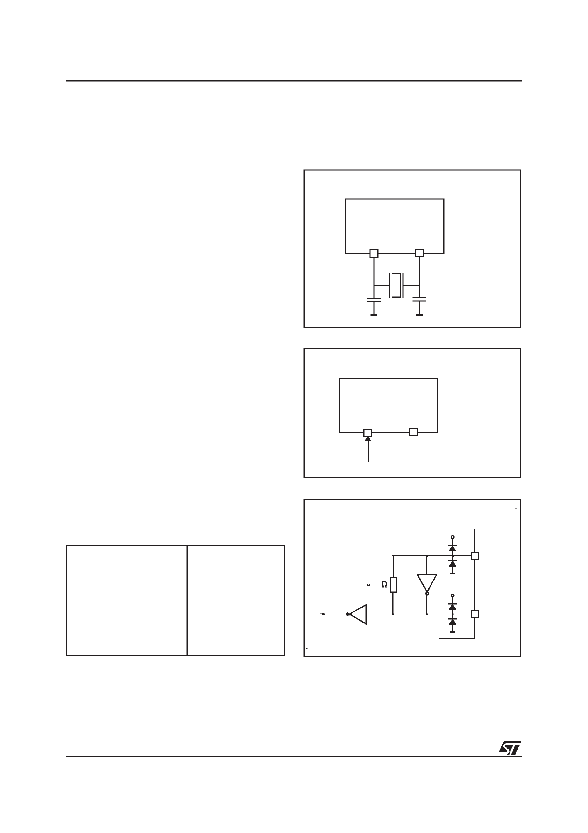
3.1 ON-CHIP CLOCK OSCILLATOR
The internal oscillator circuit is designed to require
a minimum of external components. A crystal
quartz, a ceramic resonator, or an external signal
(provided to the OSCin pin) may be used to generate a system clockwith various stability/cost tradeoffs. The typical clock frequency is 8MHz. Please
note that different frequencies will affect the operation of those peripherals (D/As, SPI) whose reference frequencies are derived from the system
clock.
The different clock generator connection schemes
are shown inFigure 1 and 2. One machine cycle
takes 13 oscillator pulses; 12 clock pulses are
needed to increment the PC while and additional
13th pulse is needed to stabilize the internal latches during memory addressing. This means that
with a clock frequency of 8MHz the machine cycle
is 1.625µSec.
The crystal oscillator start-up time is a function of
many variables: crystal parameters (especially
RS), oscillator load capacitance (CL), IC parameters, ambient temperature, and supply voltage.It
must be observed thatthe crystal or ceramic leads
and circuit connections must be as short as possible. Typical values for CL1 and CL2 are in the
range of 15pF to 22pF but these should be chosen
based on the crystal manufacturers specification.
Typical input capacitance for OSCin and OSCout
pins is 5pF.
The oscillatoroutput frequency is internally divided
by 13 to produce the machine cycle and by 12 to
produce the Timers and the Watchdog clock. A
byte cycle is the smallest unit needed to execute
any operation (i.e., increment the program counter). An instruction may need two, four, or five byte
cycles to be executed (SeeTable 1).
Table 6. Instruction Timing with 8MHz Clock
Figure 9. Clock Generator Option 1
CRYSTAL/RESONATOR CLOCK
ST6xxx
OSC
C
L1
OSC
in
out
C
L2
VA0016B
Figure 10. Clock Generator Option 2
EXTERNAL CLOCK
ST6xxx
OSC
OSC
in
out
NC
VA0015C
Figure 11. OSCin, OSCout Diagram
OSCin, OSCout (QUARTZ PINS)
V
DD
Instruction Type Cycles
Branch if set/reset 5 Cycles 8.125µs
Branch & Subroutine Branch 4 Cycles 6.50µs
Bit Manipulation 4 Cycles 6.50µs
Load Instruction 4 Cycles 6.50µs
Arithmetic & Logic 4 Cycles 6.50µs
Conditional Branch 2 Cycles 3.25µs
Program Control 2 Cycles 3.25µs
18/64
Execution
Time
OSCin
1M
In
V
DD
OSCout
VA00462
Page 19
3.2 RESETS
ST6373
The MCU can be reset in three ways:
– by the external Reset input being pulled low;
– by Power-on Reset;
– by the digital Watchdog peripheral timing out.
3.2.1 RESET Input
The RESET pin may be connected to a device of
the application board in order to reset the MCU if
required. The RESET pin may be pulled low in
RUN, WAIT or STOP mode. This input can be
used to reset the MCU internal state and ensure a
correct start-up procedure. The pin is active low
and features a Schmitt trigger input. The internal
Reset signal is generated by adding a delay to the
external signal. Therefore even short pulses on
the RESET pin are acceptable, provided VDDhas
completed its rising phase and that the oscillatoris
running correctly (normal RUN or WAIT modes).
The MCU is kept in the Reset state as long as the
RESET pin is held low.
If RESET activation occurs in RUN or WAIT
modes, processing of the user program isstopped
(RUN mode only), theInputs and Outputs are configured as inputs with pull-up resistors if available.
When the level on the RESET pin then goes high,
the initialization sequence is executed following
expiry of the internal delay period.
If RESET pin activation occurs in the STOP mode,
the oscillator starts up and all Inputs and Outputs
are configured as inputs with pull-up resistors if
available. When the level of theRESET pin then
goes high, the initialization sequence is executed
following expiry of the internal delay period.
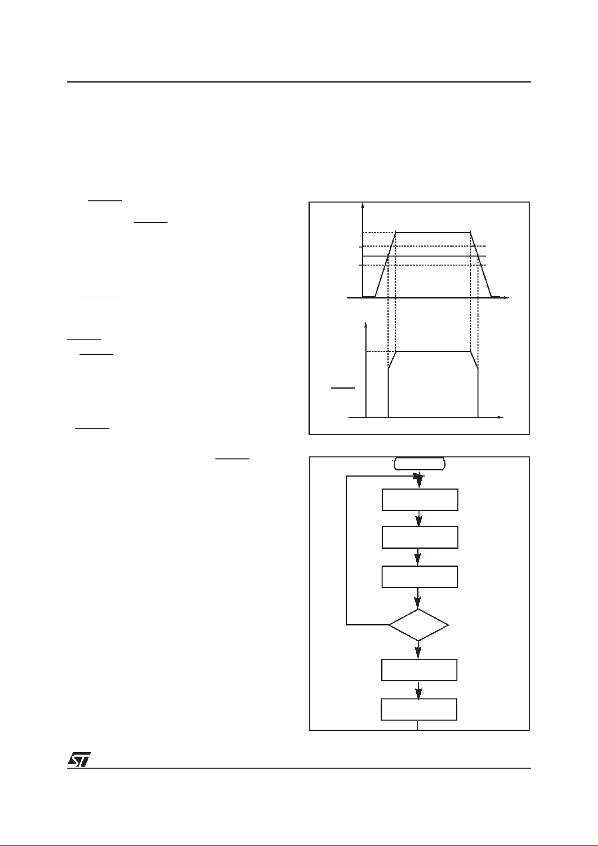
3.2.2 Power-on Reset
The function of the POR circuit consists in waking
up the MCU at an appropriate stage during the
power-on sequence. At the beginning of this sequence, the MCU is configured in the Reset state:
all I/O ports are configured as inputs with pull-up
resistors and noinstruction is executed. When the
power supply voltage rises to a sufficient level, the
oscillator starts to operate, whereupon an internal
delay is initiated, in order to allow the oscillator to
fully stabilize before executing the first instruction.
The initialization sequence is executed immediately following the internal delay.
The internal delay is generated by an on-chip
counter. Theinternal reset line is released 2048internal clock cycles after release of the external reset.
The internal POR device is a static mechanism
which forces the reset state when VDDis below a
threshold voltage in the range 3.4 to 4.2Volts (see
Figure 1).The circuit guarantees that the MCU will
exit or enter the reset state correctly, without spurious effects, ensuring, for example, that EEPROM
contents are not corrupted.
Note
: This featureisnot available on OTP/EPROM
Devices.
Figure 12. Power ON/OFF Reset operation
V
DD
4.2
Threshold
3.4
t
V
DD
POWER
ON/OFF
RESET
t
VR02037
Figure 13. Reset and Interrupt Processing
RESET
NMI MASK SET
INT LATCH CLEARED
( IF PRESENT )
SELECT
NMI MODE FLAGS
PUT FFEH
ON A DDRESSBUS
YES
IS RESET STILL
PRESENT?
NO
LOAD PC
FROM RESET LOCATION S
FFE/FFF
FETCH INSTRUCTION
VA000427
19/64
Page 20
ST6373
RESETS (Cont’d)
3.2.3 Watchdog Reset
The MCU provides a Watchdog timer function in
order to ensure graceful recovery from software
upsets. If the Watchdog register is not refreshed
before an end-of-count condition is reached, the
internal reset will be activated. This, amongst other things, resets the watchdog counter.
The MCU restarts just as though the Reset had
been generated by theRESET pin, including the
built-in stabilisation delay period.
3.2.4 Application Note
No external resistor is required between VDDand
the Reset pin, thanks to the built-in pull-up device.
3.2.5 MCU Initialization Sequence
When a reset occurs the stack is reset, the PC is
loaded with the address of the Reset Vector (located in program ROMstarting at address 0FFEh). A
jump to the beginning of theuser program mustbe
coded at this address. Following a Reset, the Interrupt flag is automatically set, so that the CPU is
in Non Maskable Interrupt mode; this prevents the
initialisation routine from being interrupted. The initialisation routine should therefore be terminated
by a RETI instruction, in order to revert to normal
mode andenable interrupts. Ifno pending interrupt
is present at theend of the initialisation routine, the
MCU will continue by processing the instruction
immediately following the RETI instruction. If, however, a pending interrupt is present, it will be serviced.
Figure 14. Reset and Interrupt Processing
RESET
JP:2 BYTES/4CYCLES
RESET
VECTOR
INITIALIZATION
ROUTINE
JP
RETI: 1 BYTE/2 CYCLES
RETI
VA00181
Figure 15. Reset Circuit
RESET
(ACTIVE LOW)
OSCILLATOR
SIGNAL
1k
V
DD
300k
TO ST6
ST6
INTERNAL
RESET
COUNTER
RESET
WATCHDOG RESET
POWER ON/OFFRESET
VA0200E
20/64
Page 21

3.3 HARDWARE ACTIVATED DIGITAL WATCHDOG FUNCTION
ST6373
The hardware activated digital watchdog function
consists of a down counter that is automatically initialized after reset so that this function does not
need to be activated by the user program. As the
watchdog function is always activated this down
counter can not be used as a timer. The watchdog
is using one data space register (HWDR location
D8h). The watchdog register is set to FEh on reset
and immediately starts to count down, requiring no
software start. Similarly the hardware activated
watchdog can not be stopped or delayed by software.
The watchdog time can be programmed using the
6 MSBs in the watchdog register, this gives the
possibility to generate a reset in a time between
3072 to 196608 oscillator cycles in 64 possible
steps. (With a clock frequency of 8MHzthis means
from 384ms to 24.576ms). The reset is prevented
if the register is reloaded with the desired value
before bits 2-7 decrement from all zeros to all
ones.
The presence of the hardware watchdog deactivates the STOP instruction and a WAIT instruction
is automatically executed instead of a STOP. Bit 1
of the watchdog register (set to one at reset) can
be used to generate a software reset if cleared to
zero). Figure 1shows the watchdog block diagram
while Figure 2shows its working principle.
Figure 16. Hardware Activated Watchdog Block Diagram
RESET
S
Q
RSFF
R
-2
DB1.7 SETLOAD
7
-2
SET
8
-12
DB0
8
WRITE
DATA BUS
OSCILLATOR
CLOCK
RESET
VA00010
21/64
Page 22

ST6373
HARDWARE ACTIVATED DIGITAL WATCHDOG FUNCTION (Cont’d)
Hardware Activated Watchdog Register
(HWDR)
Address: D8h - Read/Write
Reset Value: 0FEh
70
Figure 17. Hardware Activated Watchdog
Working Principle
D0
BIT7
T1 T2 T3 T4 T5 T6 SR C
T1-T6. These are the watchdog counter bits. It
should be noted that D7 (T1) is the LSB of the
counter and D2 (T6) is the MSB of the counter,
these bits are in the opposite order to normal.
SR. This bit is set to one during the reset phase
and will generate a software reset if cleared to zero.
C. This is the watchdog activation bit that is hardware set. The watchdog function is always activated independently of changes of value of this bit.
The register reset value is FEh (Bit 1-7 set to one,
Bit 0 cleared).
D1
D2
D3
D4
D5
D6
D7
BIT6
BIT5
BIT4
BIT3
BIT2
WATCHDOG CONTROL REGISTER
BIT1
BIT0
8-BIT
DOWN COUNTER
RESET
OSC-12
VA00190
22/64
Page 23

3.4 INTERRUPT
ST6373
The MCU Core can manage 4 different maskable
interrupt sources, plus one non-maskable interrupt
source (top priority level interrupt). Each source is
associated with a particular interrupt vector that
contains a Jump instruction tothe related interrupt
service routine. Each vector is located in the Program Space at a particular address (see Table 7).
When a source provides an interrupt request, and
the request processing is also enabled by the
MCU Core, then the PC register is loaded with the
address of the interrupt vector (i.e. of theJump instruction). Finally, the PC executes the Jump instruction and the interrupt routine is processed.
The relationship between vector and source and
the associated priority is hardware fixed for
ST6373 devices. For some interrupt sources it is
also possible to select by software the kind of
event that will generate the interrupt.
All interrupts can bedisabled by writing tothe GEN
bit (global interrupt enable) of the interrupt option
register (address C8h). Following a reset, the
ST6373 is in non maskable interrupt mode, so no
interrupts will be accepted and NMI flags will be
used, until a RETI instruction is executed. If aninterrupt is executed, one special cycle is made by
the core, during that the PC is set to the related interrupt vector address. A jump instruction at this
address has to redirect program execution to the
beginning of the related interrupt routine. The interrupt detecting cycle, also resets the related interrupt flag (not available to the user), so that another interrupt can be stored for this current vector,
while its driver is under execution.
If additional interrupts arrive from the same
source, they will be lost. NMI can interrupt other interrupt routines at any time, while other interrupts
cannot interrupt each other. If more than one interrupt is waiting for service, they are executed according to their priority. The lower the number, the
higher the priority. Priority is, therefore, fixed. Interrupts are checked during the last cycle of an in-
struction (RETI included). Level sensitive interrupts have to be valid during this period.
Table 7 details the different interrupt vectors/sources relationships.
3.4.1 Interrupt Vectors/Sources
The MCU Core includes 5 different interrupt vectors in order to branch to 5 different interrupt routines. The interrupt vectors are located in the fixed
(or static) page of the Program Space.
Table 7. Interrupt Vectors/Sources
Relationships
Interrupt Source
NMI pin
Timer 3
I/O Port A, I/O Port B
Timer 2
ADC
I2C
SPI
VSYNC,
Timer 1
DDC SPI
PWRIN
Associated
Vector
Interrupt
Vector # 0 (NMI)
Interrupt
Vector # 1
Interrupt
Vector #2
Interrupt
Vector #3
Interrupt
Vector #4
Vector
Address
0FFCh-0FFDh
0FF6h-0FF7h
0FF4h-0FF5h
0FF2h-0FF3h
0FF0h-0FF1h
The interrupt vector associated with the nonmaskable interrupt source is named interrupt vector #0. Itis located at the (FFCh, FFDh) addresses
in the Program Space. This vector is associated
with the NMI pin.
The interrupt vectors located at addresses
(FF6h,FF7h), (FF4h,FF5h), (FF2h,FF3h),
(FF0h,FF1h) are named interrupt vectors #1, #2,
#3 and #4 respectively. These vectors are associated with TIMER 3, Port A and Port B interrupts
(#1), Timer 2, VSYNC and I2C SPI (#2), TIMER 1
and the DDC SPI (#3) and the ADC and PC4
(PWRIN) (#4).
23/64
Page 24

ST6373
INTERRUPTS(Cont’d)
3.4.2 Interrupt Priority
The non-maskable interrupt request has the highest priority and can interrupt any other interrupt
routines at any time, nevertheless the other interrupts cannot interrupt each other. If more than one
interrupt request is pending, they are processed
by the MCU Core according to their priority level:
vector #1 has the higher priority while vector #4
the lower. The priority of each interrupt source is
hardware fixed.
3.4.3 Interrupt Option Register
The Interrupt Option Register (IOR register, location C8h) is used to enable/disable the individual
interrupt sources and to select the operating mode
of the external interrupt inputs. This register is addressed in the Data Space as a RAM location at
address C8h, nevertheless it is write-only register
that can not be accessed with single-bit operations. The operating modes of the external interrupt inputs associated to interrupt vectors #1 and
#2 are selected through bits 4 and 5 of the IOR
register.
Interrupt Option Register (IOR)
Address: (C8h) - Write only
Reset Value: XX00XXXXb
70
-
EL1 ES2 GEN ----
D7
. Not used.
EL1. This is the Edge/Level selection bit of interrupt #1. When set to one, the interrupt is generated on low level of the related signal; when cleared
to zero, the interrupt is generated on falling edge.
The bit is cleared tozero after reset.
ES2
. This is the edge selection bit on interrupt #2.
This bit is used in ST6373 devices for VSYNC detection, the interrupt for Timer 2 and the I2CSPI.It
is cleared to zero on reset (falling edge), and must
be maintained at 0 ifthe Timer 2 and I2C interrupts
are to be used. The VSYNC interrupt may be configured to act on the falling edge (ES2=0) or rising
edge (ES2=1) according to the system design.
GEN
. This is the global enable bit. When set to
one all interrupts are globally enabled; when this
bit is cleared to zeroall interrupts are disabled (excluding NMI) independently to the individual interrupt enable bitof each peripheral.
D3 - D0
. These bits are not used.
NMI/PWR/VSync Interrupt Register (NPVIR)
70
D7 D6 D5 D4 D3 D2 D1 D0
b7: VSYNCST: (Read & Write, 0 written on Reset)
VSYNCEN
b6:
: (Read & Write, 0 written on Reset)
b5:PWRFLAG:(Read&Write,UndefinedonReset)
b4: PWINTEN: (Write Only, 0 written on Reset)
PWREDGE
b3:
: (Write Only, 0 written on Reset)
b2:NMIFLAG:(Read &Write,UndefinedonReset)
b1: NMINTEN: (Write Only, 0 written on Reset)
b0: NMIEDGE: (Write Only, 0 written onReset)
Note thatNObit operation instructionsare possible.
The input latch is activatedoneither the positive or
negative edge of the NMI (respectively PWRIN)
signal: if NMIEDGE (resp. PWREDGE) is high the
latch will be triggered onthe rising edge of the signal at NMI (resp. PWRIN); if thisbit is low the latch
will be triggered on the falling edge.
An interrupt can be generated if it is enabled: if
NMINTEN (resp. PWINTEN) is high, then the output of the latch may generate an interrupt on vector #0 (resp. vector #4); if this bit is low the interrupt is disabled.
The status of the latch is read with NMIFLAG (resp. PWRFLAG): if NMIFLAG (resp. PWRFLAG) is
high, a signal has been latched. The latch can be
reset by setting NMIFLAG (resp. PWRFLAG).
The VSYNC input is linked to the interrupt vector#
2 through a latch.
If 1 is written in VSYNCST the latch will be triggered on the rising edge of the signal at VSYNC, if
VSYNCST is low the latch will be triggered on the
falling edge (0 written on Reset).
An interrupt can be generated only if VSYNCEN is
at 1. Writing a 1 in VSYNCEN will also reset the
latch (0 written on Reset).
The status of the latch is read through the bit
VSYNCEN; reading a 1 means that a signal has
been latched.
The status of the VSYNC pin is read with the
VSYNCST bit.
24/64
Page 25

INTERRUPTS(Cont’d)
3.4.4 Interrupt Procedure
The interrupt procedure is very similar toa call procedure; the user can consider the interrupt as an
asynchronous call procedure. As this is an asynchronous event the user does not know about the
context and the time at which it occurred. As a result the user should save all the data space registers which will be used inside the interrupt routines. There are separate sets of processor flags
for normal, interrupt and non-maskable interrupt
modes which are automatically switched and so
these do not need to be saved.
The following list summarizes the interrupt procedure (refer also to Figure 20. Interrupt Processing
Flow Chart):
– Interrupt detection
– The flags C and Z of the main routine are ex-
changed with the flags C and Z of the interrupt
routine (resp. the NMI flags)
– The value of the PC is stored in the first level of
the stack - The normal interrupt lines are inhibit-
ed (NMI still active)
– The edge flip-flop is reset
– The related interrupt vector is loaded in the PC.
– User selected registers are saved inside the in-
terrupt service routine (normally on a software
stack)
– The source of the interrupt is found by polling (if
more than one source is associated to the same
vector)
– Interrupt servicing
– Return from interrupt (RETI)
– Automatically the MCU Core switches back to
the normal flags (resp. the interrupt flags) and
pops the previous PC value from the stack
The interrupt routine begins usually by the identifi-
cation of the device that has generated the interrupt request. The user should save the registers
which are used inside the interrupt routine (that
holds relevant data) into asoftware stack.
After the RETI instruction execution, the Core carries out the previous actions and the main routine
can continue.
ST6373
Figure 18. Interrupt Processing Flow-Chart
INSTRUCTION
FETCH
INSTRUCTION
EXECUTE
INSTRUCTION
WAS
THE INSTRUCTION
A RETI
YES
YES
NO
?
NO
CLEAR
INTERRUPT MASK
SELECT
PROGRAM FLAGS
” POP ”
THE STACKED PC
?
YES
3.4.5 ST6373 Interrupt Details
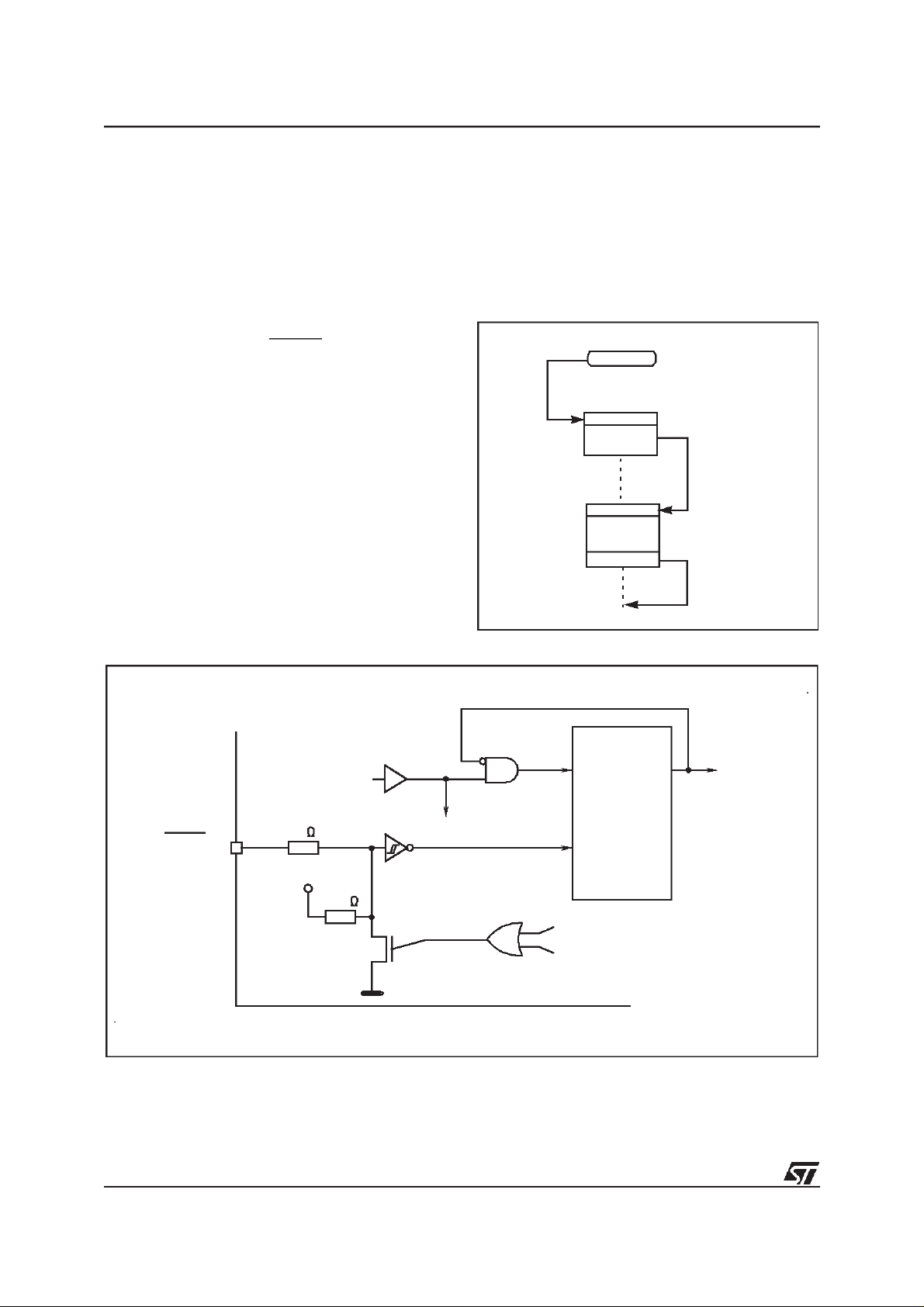
Interrupt #0. The NMI Interrupt is connected to the
first interrupt #0 (NMI, Pin 27). If the NMIinterrupt
is disabled at the latch circuitry, then it willbe high.
The #0 interrupt input detects a high to low level.
Note that once #0 has been latched, then the only
way to remove the latched #0 signal is to service
the interrupt. #0 can interrupt the other interrupts.
NO
IS THE CORE
ALREADY IN
NORMAL MODE ?
INTERNAL MODE FLAG
CHECK IF THERE IS
AN INTERRUPT REQUEST
AND INTERRUPT MASK
LOAD PC FROM
INTERRUPT VECTOR
( FFC / FFD )
SET
INTERRUPT MASK
PUSH THE
PC INTO THE STACK
SELECT
VA000014
25/64
Page 26

ST6373
INTERRUPTS(Cont’d)
Interrupt #1. The TIMER 3 Interrupt and the Port
A and B interrupts are connected by a logical AND
function to interrupt #1 (0FF6h). The TIMER 3 interrupt generates a low level (which is latched in
the timer) requiring that the Interrupt 1 Edge/Level
bit is set to 1. The I/O Port A and B interrupts may
be set to generate an interrupt on the falling edge
or low level state of the input (EL1 = 1 or EL1 = 0
respectively) according to the external connections.Note that if a low level is maintained on an
I/O bit configured as acting on a Low Level after
the interrupt is generated, the MCU will return to
the interrupt state after exiting the RETI instruction
from the first interrupt service.
Interrupt #2.The VSYNC, Timer 2 and I2C SPI In-
terrupt areconnected by a logical AND function to
interrupt #2. Bit 5 of the interrupt option register
C8h is used to select the negative edge (ES2=0)
or the positive edge (ES2=1) to trigger the interrupt #2.For the correct operation of the Timer 2
and I2C SPI interrupts, the falling edge should be
selected (ES2 = 0).For theVSYNC interrupt, either
edge can be selected, depending on the operation
required. For example if the rising edge on VSYNC
is the trigger, and after receiving the interrupt
edge, the VSYNC trigger level is switched to the
falling edge, the time between the risingand falling
edge (e.g. the display time)to be determined. The
VSYNC interrupt is controlled in Register NPVIR
at address EDh.
Note that once an edge has beenlatched, then the
only way to remove the latched signalis to service
the interrupt. Care must be taken not to generate
spurious interrupts. For example, changing the
edge selection bit from falling edge to rising edge
when the VSYNC input is high (or disabled in NP-
VIR) will cause a spurious interrupt.(see Interrupt
Circuit Diagram)
Interrupt #3
. The TIMER 1 and DDCSPI Interrupt
are connected by a logical AND function to interrupt #3. This interrupt is triggered ondetection of a
low level latched in the timer and DDC SPI.
Interrupt #4
. The PWRIN and Analog to Digital
Converter Interrupts are connected by a Logical
AND to interrupt #4 (0FF0h). The PWRINinterrupt
is controlled through the NPVIR Register at address EDh, and the Phase Unlock interrupt is controlled through SPCR at address DFh. The #4 interrupt input detects a low level. A simple latch is
provided from the PC4 (PWRIN) pin in order to
generate the PWRINT signal. This latch can be
triggered by either the positive or negative edge of
the PWRIN signal (bit 3, PWREDGE, of register
NPVIR EDh). The latch isreset by software.
Notes
:
Global disable does not reset edge sensitive interrupt flags.These edge sensitive interrupts become
pending again when global disabling is released.
Moreover, edge sensitive interrupts are stored in
the related flags also when interrupts are globally
disabled, unless each edge sensitive interrupt is
also individually disabled before the interrupting
event happens. Global disable is done by clearing
the GEN bit of Interrupt option register, while any
individual disable is done in the control register of
the peripheral. The on-chip Timer peripherals
have an interrupt request flag bit (TMZ), this bit is
set to one when the device wants to generate an
interrupt request and a mask bit (ETI) that must be
set to one to allow the transfer of the flag bit to the
Core.
26/64
Page 27

INTERRUPTS(Cont’d)
Figure 19. Interrupt Circuit Diagram
START FROM
RE
ST6373
IT
VA0426Q
STOP/WA
(FF2,3)
INT #3
Start
2
I
IORREG.C8H,bit5
FF
INT #2 (FF4,5)
CLR
CLK Q
INT #1 (FF6,7)
INT #0 - NMI (FFC,D)
Start
0
I
FF
CLR
CLK Q
FF
NPVIR Bit 2
CLR
CLK Q
NPVIR Bit 0
NPVIR BIT 1
FF
0
QCLK
CLR
1
MUX
IORREG.C8H,bit6
Start
1
I
INT #4 (FF0,1)
h, bit 4 : GEN
IOR REGC
ADC
ADCR Bit 7SLACR Bit 1
NPVIR Bit 4
QCLK
NPVIR Bit 5
FF
CLR
V
DD
DD
V
2
I C SPI
PBE
SINGLE BIT ENABLE
FROM REGISTER PORT A,B
NMI
PBEPBE
A,B
PORT
TIMER 3
TSCR3 Bit 6
DD
V
Bits
TIMER 2
NPVIR Bit 6
SYNC
V
SCR1 Bit 5
TSCR2 Bit 6
PI
TIMER 1
DDC S
SCR1 Bit 5
TSCR1 Bit 6
DD
V
NPVIR Bit 3
PC4/PWRIN
27/64
Page 28

ST6373
3.5 POWER SAVING MODES
STOP and WAIT modes have been implemented
in the ST638x in order to reduce the current consumption of the device during idle periods. These
two modes are described in the following paragraphs. Since the hardware activated digital
watchdog function is present, the STOP instruction is de-activated and any attempt to execute it
will cause the automatic execution of a WAIT instruction.
3.5.1 WAIT Mode
The configuration of the MCU in the WAIT mode
occurs as soon as the WAIT instruction is executed. The microcontroller can also be considered as
being in a “software frozen” state where the Core
stops processing the instructions of the routine,
the contents of the RAM locations and peripheral
registers are saved as long as the power supply
voltage is higher than the RAM retention voltage
but where the peripherals are still working. The
WAIT mode is used when the user wants to reduce the consumption of the MCU when it is in
idle, while not losing count of time or monitoring of
external events. The oscillator is not stopped in order to provide clock signal to the peripherals. The
timers counting may be enabled (writing the PSI
bit in TSCR1 register) and the timer interrupt may
be also enabled before entering the WAIT mode;
this allows the WAIT mode to be left when timer interrupt occurs. If the exit from the WAIT mode is
performed with a general RESET (either from the
activation of the external pin or by watchdog reset)
the MCU will enter a normal reset procedure as
described in the RESET chapter. If an interrupt is
generated during WAIT mode the MCU behaviour
depends on the state of the MCU Core before the
initialization ofthe WAIT sequence, but also of the
kind of the interrupt request that is generated. This
case will be described in the following paragraphs.
In any case, the MCU Core does not generate any
delay afterthe occurrence of the interrupt because
the oscillator clock is still available.
3.5.2 STOP Mode
Since the hardware activated watchdog is present
on the ST638x, the STOP instruction has been deactivated. Any attempt to execute a STOP instruction will cause a WAIT instruction to be executed
instead.
3.5.3 Exit from WAIT Mode
The following paragraphs describe the output procedure of the MCU Core from WAIT mode when
an interrupt occurs. It must be noted that the restart sequence depends onthe original stateof the
MCU (normal, interrupt or non-maskable interrupt
mode) before the start of the WAIT sequence, but
also of the typeof theinterrupt request that is generated. In all cases the GEN bit of IOR has to be
set to 1 in order to restart from WAIT mode. Contrary to the operation of NMI in the run mode, the
NMI is masked in WAIT mode if GEN=0.
Normal Mode. If the MCU Core was in the main
routine when the WAIT instruction has been executed, the Core exits from WAIT mode as soon as
an interrupt occurs; the corresponding interrupt
routine is executed, and at the end of the interrupt
service routine, the instruction that follows the
WAIT instruction is executed if no other interrupts
are pending.
Non-maskable Interrupt Mode
. If the WAIT instruction has been executed during the execution
of the non-maskable interrupt routine, the MCU
Core outputs from WAIT mode as soon as any interrupt occurs: the instruction that follows the
WAIT instruction is executed and the MCU Core is
still in the non-maskable interrupt mode even if another interrupt hasbeen generated.
Normal Interrupt Mode. If the MCU Core was in
the interrupt mode before the initialization of the
WAIT sequence, it outputs from the wait mode as
soon as any interrupt occurs. Nevertheless, two
cases have to be considered:
– If the interrupt is a normal interrupt, the interrupt
routine in which the WAIT was entered will be
completed with the execution of the instruction
that follows the WAIT and theMCU Core is still in
the interrupt mode. At the end of this routine
pending interrupts will be serviced in accordance
to their priority.
– If the interrupt is a non-maskable interrupt, the
non-maskable routine is processed at first.Then,
the routine in which the WAIT was entered will be
completed with the execution of the instruction
that follows the WAIT and theMCU Core is still in
the normal interrupt mode.
Notes
:
If all the interrupt sources are disabled, the restart
of the MCU can only be done by a Reset activation. The Wait instruction is not executed if an enabled interrupt request is pending. In ST638x devices, the hardware activated digital watchdog
function is present. As the watchdog is always activated, the STOP instruction is de-activated and
any attempt to execute the STOP instruction will
cause an execution of a WAIT instruction.
28/64
Page 29

4 ON-CHIP PERIPHERALS
4.1 I/O PORTS
ST6373
The ST6373 microcontroller uses three I/O ports
(A,B,C) with up to eight pins on each port. Each
line can be individually programmed either in the
input mode or the output mode with the following
software selectable options:
– Input without interrupt and without pull-up (Ports
A, B and C)
–Input withpull-up andwithinterrupt (PA0-PA5and
Port B)
– Inputwith pull-up without interrupt (PA0-PA5 and
Port B, PC2-PC7)
– Analog Inputs (PB0-PB7)
– Open-drain output 12V, no pull-up (PC4-PC7)
– Open-drain output 5V (PA0-PA7, PB0-PB7,
PC0-PC3)
– Push-pull output (PA0-PA5, PB0-PB7)
– SPI control signals (PA6,PA7 for I2C SPI,
PC0,PC1,PC3 for DDC SPI)
– Horizontal Timing inputs (PC6/HSYNC,
PC7/HDRIV
– External Power In Interrupt (PC4)
The lines are organized in three ports (Ports A, B,
C). The ports occupy 8 registers in the data space.
Each bit ofthese registers isassociated with a particular line (for instance, the bits 0 of the Port A Data, Direction and Option registers are associated
with the PA0 line of Port A).
The three Data registers (DRA, DRB, DRC) are
used to read the voltage level values of the lines
programmed in theinput mode, or to write the logic
value of the signal to be output on the lines configured in the output mode. The port Data Registers
can be read to get the effective logic levels of the
pins, but they can be also written by the user software, in conjunction with the related Data Direction Register and Option Register (Ports A and B
only), to select the different input mode options.
Single-bit operations on I/O registers (bit set/reset
instructions) are possible but care is necessary
because reading in input mode is made from I/O
pins and therefore might be influenced by the external load, while writing will directly affect the Port
data register causing an undesired changes of the
input configuration.
The three Data Direction registers (DDRA, DDRB,
DDRC) allow the selection of the direction of each
pin (input or output).
The two Option registers (ORAand ORB) are used
to select the different port options available both in
input and in output mode for Ports A and B only.
All the I/O registers can be read or written as any
other RAM location of the data space, so no extra
RAM cell is needed for port data storing and manipulation. During the initialization of the MCU, all
theI/Oregistersarecleared and theinputmodewith
pull-up is selected on all the pins thus avoiding pin
conflicts (with the exception of PC2 which is set to
output mode with the value 1 (high impedance).
Figure 20. I/O Port Block Diagram (PA0-PA5 and Port B)
S
CONTROLS
IN
SHIFT
REGISTER
S
OUT
TO INTE RRUPT
TO AD C
RESET
DATA
DIRECTION
REGISTER
DATA
REGISTER
OPTION
REGISTER
V
DD
V
DD
INPUT/OUTPUT
VA000413
29/64
Page 30

ST6373
I/O PORTS (Cont’d)
4.1.1 Details of I/O Ports A and B
Each pin of Ports A and B can be individually programmed as input or output with different input
and output configurations.
This is achieved by writing the relevant bit in the
data register (DR), data direction register (DDR)
and option register (OR). Table 8 shows all the
port configurations that can be selected by user
software.
4.1.1.1 Input Option Description
Pull-up, High Impedance Option
. All the input
lines can be individually programmed with or without an internal pull-up according to the codes programmed in the ORand DR registers. Ifthe pull-up
Table 8. I/O Port Options Selection (Ports A and B only)
DDR OR DR Mode Option
0 0 0 Input With pull-up, no interrupt (Reset state)
0 0 1 Input No pull-up, no interrupt
0 1 0 Input With pull-up, with interrupt
011
1 0 X Output Open-drain output (10mA sink current for Port A pins)
1 1 X Output Push-pull output (10mA sink current for Port A pins)
Input No pull-up, no interrupt (Port A pins)
Input Analog input (Port B pins)
is not selected, the input pin is in the high impedance state.
Interrupt Option
. All the input lines can be individually connected by software totheinterrupt linesof
the MCU core according to the codes programmed
in the OR and DR registers. The pins of Port A and
B are “ORed” and are connected to the interrupt
associated to the vector #1.
Analog Input Option. The PB0-PB7 pins can be
configured to be analog inputs according to the
codes programmed in the OR and DR registers.
These analog inputs are connected to the on-chip
8-bit Analog to Digital Converter. ONLY ONE pin
should be programmed as analog input at a time,
otherwise the selected inputs will be shorted.
Note X: Means don’t care.
30/64
Page 31

I/O PORTS (Cont’d)
4.1.1.2 Output Option Description
Output Option
Port A and B pins in output modes can be set to
Open Drain or Push-Pull modes (not for PA6 and
PA7). Port A bits set to output have a maximum
10mA current sink LED drive capability.
4.1.1.3 I2C SPI Input/Output
If the user uses the I2C serial peripheral interface,
the I/Olines PA6 and PA7 should be set in output
mode with the open-drain configuration; the corresponding data bit must set to one.
Note
. Switching the I/O ports with interrupt (Ports
A and B) from one state to another should be done
in a way that no unwanted side effects can happen. The recommended safe transitions are
shown below. All other transitions are risky and
should be avoided during change of operation
mode as it is most likely that there will be an unwanted side-effect such as interrupt generation or
two pins shorted together by the analog input
lines.
Single bit instructions (SET, RES, JRR and JRS)
should be used very carefully with Port A and B
data registers because these instructionsmake an
implicit read and write back of the whole addressed register byte. In port input mode however
data register address reads from input pins, not
from data register latches and data register information in input mode is used to set characteristics
therefore these characteristics may be unintentionally reprogrammed, depending on the state of
input pins. As general rule isbetter to use single bit
instructions on data register only when the whole
port is in output mode. If input or mixed configuration is needed itis recommended tokeep a copyof
the data register in RAM. On this copy it is possible
to use single bit instructions, then the copy register
could be written into the port data register.
SET bit, datacopy
LD a, datacopy
LD DRA, a
4.1.2 Details of I/O Port C
Port C
. When programmed as an input aninternal
pull-up can be switched active under program control. When programmed as an output the Port C
I/O pins will operate inthe open-drain mode. PC0PC3 are available as open-drain capable of withstanding a maximum VDD+0.3V. PC4-PC7 are
available as open-drain capable of withstanding
12V and have no resistive pull-up in input mode.
If the user uses the DDC serial peripheral interface, the I/O lines PC0 and PC1 should be set in
output mode while the open-drain configuration is
hardware fixed; the corresponding data bit must
set to one.If the latched interrupt functions are
used (HSYNC,(HSYNC, HDRIVE, PWRIN) then
the corresponding pins should be set to input
mode.
of the input pin (interrupt, pull-up, analog input),
Figure 21. State Transition Diagram for Safe Transitions (Ports A and B)
ST6373
Interrupt
pull-up
Input
pull-up (Reset
state)
Output
Open Drain
Output
Push-pull
Note
*.xxx = DDR,OR, DR bits respectively
010*
000
100
110
011
001
101
111
Input
Analog
Input
Output
Open Drain
Output
Push-pull
31/64
Page 32

ST6373
I/O PORTS (Cont’d)
Table 9. I/O Port Option Selections
MODE AVAILABLE ON
PA0-PA7
Input
PB0-PB7
PC0-PC7
Input
with pull up
Input
with pull up
with interrupt
PA0-PA5
PB0-PB7
PC2, PC3
PA0-PA5
PB0-PB7
(1)
SCHEMATIC
Data in
Interrupt
Data in
Interrupt
Data in
Interrupt
Analog Input PB0-PB7
Open drain output
5mA / V
DD
+0.3V
Open drain output
10mA / V
DD
+0.3V
Open drain output
PB0-PB7
PC0-PC7
PA0-PA7
PC4-PC7
5mA / 12V
Push-pull output
PB0-PB7
5mA
Push-pull output
PA0-PA5
10mA
Note 1
. Provided the correct configuration has been selected.
ADC
Data out
Data out
32/64
Page 33

I/O PORTS (Cont’d)
4.1.2.1 Port C I/O Pin Programming
Each Port C pin can be individually programmed
as input or output. This is achieved by writing to
the relevant bit in the data (DRC) and data direction register (DDRC). Table 9 shows all the port
configurations that can be selected by the user
software.
4.1.2.2 Port C Input/Output Configurations
The following schematics show the I/O lines hardware configuration for the different options. Figure
31 shows the I/O configuration for an I/O pin with
open-drain 12V capability (standard drive and high
drive). Figure 32 shows the I/O configuration for an
I/O pin with open-drain 5V capability.
Note:
All the Port A, B and C I/O lines have Schmitt-trig-
ger input configuration with a typical hysteresis of
1V.
ST6373
Table 10. I/O Port Options Selection (Port C)
DDR DR Mode Option
0 0 Input With on-chip pull-up resistor
0 1 Input Without on-chip pull-up resistor
1 X Output Open-drain
Note
: X. Means don’t care.
Figure 22. I/O Configuration Diagram
(Open Drain 12V)
I/O HIGH DRIVE, OPEN DRAIN 12V
Out
In
N
I/O
(5mA, 1V)
VA00342
Figure 23. I/O Configuration Diagram (Open Drain 5V)
OPEN-DRAIN OUTPUT
*
In
Out
*
In Input mode only, SW programmable ( 200k )
N
V
DD
I/O (OPEN-DRAIN, 5V)
~
VA00345A
33/64
Page 34

ST6373
4.1.3 I/O Port Registers
4.1.3.1 Data Registers
Ports A, B, C Data Register
Address:C0h (PA), C1h (PB), C2h (PC)
Read/Write
Reset Value: 00h
70
PA/PB
PA/PB
PA/PB
PA/PB
PA/PB
PA/PB
PA/PB
/PC7
/PC6
/PC5
/PC4
/PC3
/PC2
/PC1
PA/PB
/PC0
PA7-PA0. These are the I/O Port A data bits. Reset at power-on.
PB7-PB0
. These are the I/O Port B data bits. Re-
set at power-on.
PC7-PC0
. These are the I/O Port C data bits. Set
to 04H at power-on. Bit 2 (PC2 pin) is set to one
(open-drain therefore high impedance).
4.1.3.2 Data Direction Registers
Ports A, B, C Data Direction Register
Address: C4h (PA), C5h (PB), C6h (PC) Read/Write
Reset Value: 00h
70
PA/PB
PA/PB
PA/PB
PA/PB
PA/PB
PA/PB
PA/PB
/PC7
/PC6
PA7-PA0
/PC5
/PC4
/PC3
/PC2
. These are the I/O Port A data direction
/PC1
PA/PB
/PC0
bits. When a bit is cleared to zero the related I/O
line is in input mode, if bit is set to one the related
I/O line is in output mode. Reset at power-on.
PB7-PB0
. These are the I/O Port B data direction
bits. When a bit is cleared to zero the related I/O
line is in input mode, if bit is set to one the related
I/O line is in output mode. Reset at power-on.
PC7-PC0
-
bits. When a bit is cleared to zero the related I/O
. These are the I/O Port C data direction
line is in input mode, if bit is set to one the related
I/O line is in output mode. Set to 04H at power-on.
Bit 2 (PC2 pin) is set to one (output mode selected).
4.1.3.3 Option Registers
Port A, B, C Option Register
Address: CCh (PA), CDh (PB) - Read/Write
Reset value:00h
70
PA/PB7PA/PB6PA/PB5PA/PB4PA/PB3PA/PB2 PA/PB1 PA/PB0
PA7-PA0.
These are the I/O Port A option bits.
These are set in conjunction with the corresponding dataand data direction bits toset the individual
Port A bit I/O mode.
PB7-PB0
. These are the I/O Port B option bits.
These are set in conjunction with the corresponding dataand data direction bits toset the individual
Port B bit I/O mode.
Notes
: The WAIT instruction allows the MCUto be
used insituations where low power consumption is
required. This can only be achieved, however, if
the I/O pins are programmed as inputs with well
defined logic levels or have no power consuming
resistive loads inoutput mode.
Single-bit operations on I/O registers are possible
but care is necessary because reading in input
mode is from I/O pins while writing will directly affect the Port data register.
34/64
Page 35

4.2 TIMERS
ST6373
The ST638x devices offer two on-chip Timer peripherals consisting of an 8-bit counter with a 7-bit
programmable prescaler, thus giving a maximum
count of 215, and a control logic that allows configuration the peripheral operating mode. Figure 1
shows the Timer block diagram. The content of the
8-bit counters can be read/written in the Timer/Counter registers TCR that are addressed in
the data space as RAM locations at addresses
D3h (Timer 1), DBh (Timer 2). The state of the 7bit prescaler can be read in the PSC register at addresses D2h (Timer 1) and DAh (Timer 2). The
control logic is managed by TSCR registers at D4h
(Timer 1) and DCh (Timer 2) addresses as described in the following paragraphs.
The following description applies to all Timers. The
8-bit counter is decrement by the output (rising
edge) coming from the 7-bit prescaler and can be
loaded and read under program control. When it
decrements to zero then theTMZ(timer zero) bit in
the TSCR is set to one. If the ETI (enable timer interrupt) bit in the TSCR isalso set to one an interrupt request, associated to interrupt vector #3 for
Timer 1 and #1 for Timer 2, is generated. The interrupt of the timer can be used to exit the MCU
from the WAIT mode.
Figure 24. Timer Peripheral Block Diagram
The prescaler decrements on rising edge. The
prescaler input is the oscillator frequency divided
by 12. Depending on the division factor programmed by PS2/PS1/PS0 (seeTable 1 ) bits in
the TSCR, the clock input of the timer/counter register is multiplexed to different sources. On division factor 1, the clock input of the prescaler is
also that of timer/counter; on factor 2,bit 0 of prescaler register is connected to the clock input of
TCR.
This bit changes its state with the half frequency of
prescaler clock input. On factor 4, bit 1 of PSC is
connected to clock input of TCR, and so on. On division factor 128, theMSB bit 6 of PSC is connected toclock inputof TCR. The prescaler initialize bit
(PSI) in the TSCRregister must be set to one to allow the prescaler (and hence the counter) to start.
If it is cleared to zero then all of the prescaler bits
are set to one and the counter is inhibited from
counting.The prescaler can be given any value between 0 and 7Fh by writing to the related register
address, if bit PSI in the TSCR register is set to
one. The tap of the prescaler is selected using the
PS2/PS1/PS0 bits in the control register.Figure 2
illustrates the Timer working principle.
TIMER
PSC
f
OSC
DATABUS 8
8
6
5
4
3
2
1
0
:12
SELECT
1OF8
SYNCHRONIZATION
LOGIC
8
8-BIT
COUNTER
8
b5
b7 b6
TMZ ETI TOUT
3
LATCH
b4 b3 b2
STATUS/CONTROL
REGISTER
DOUT
b1 b0
PSI
PS2
PS1 PS0
INTERRUPT
LINE
VA00009
35/64
Page 36

ST6373
TIMERS (Cont’d)
4.2.1 Timer Operating Modes
Since in the ST638x devices the external TIMER
pin is not connected, the only allowed operating
mode is the output mode, which is selected by setting bit 4 and by clearing bit 5 in the TSCR1 register. This procedure will enable Timer 1 and
Timer 2.
Output Mode (TSCR1 D4 = 1, TSCR1 D5 = 0).On
this mode the timer prescaler is clocked by the
prescaler clock input (OSC/12). The user can select the desired prescaler division ratio through the
PS2/PS1/PS0 bits. When TCR count reaches 0, it
sets the TMZ bit in the TSCR.
The TMZ bit can be tested under program control
to perform timer functions whenever it goes high.
Bits D4 and D5 on TSCR2 (Timer 2) register are
not implemented.
Timer Interrupt
When the counter register decrements tozero and
the software controlled ETI (enable timerinterrupt)
bit is set toone then an interrupt request associated to interrupt vector #3 (for Timer 1), to interrupt
Figure 25. Timer Working Principle
vector #1 (for Timer 2) is generated. When the
counter decrements to zero also the TMZ bit in the
TSCR register is set to one.
Notes:
TMZ is set when the counter reaches 00h; howev-
er, it may be set by writing 00h in the TCRregister
or setting the bit 7 of the TSCR register. TMZ bit
must be cleared by user software when servicing
the timer interrupt to avoid undesired interrupts
when leaving the interrupt service routine. Afterreset, the 8-bit counter register is loaded to FFh
while the 7-bit prescaler is loaded to 7Fh, and the
TSCR register is cleared which means that timer is
stopped (PSI=0) and timer interrupt disabled.
A write to the TCR register will predominate over
the 8-bit counter decrement to 00h function, i.e. if a
write and a TCR register decrement to 00h occur
simultaneously, the write will take precedence,
and the TMZ bit is not set until the 8-bit counter
reaches 00h again. Thevalues of the TCR and the
PSC registers can be read accurately at any time.
CLOCK
7-BIT PRESCALER
BIT0 BIT1 BIT2
10234
BIT0 BIT1
BIT2
BIT3
8-1 MULTIPLEXER
BIT3 BIT4 BIT5
8-BIT COUNTER
BIT5BIT4
5
BIT6
BIT6
67
BIT7
PS0
PS1
PS2
VA00186
36/64
Page 37

TIMERS (Cont’d)
4.2.2 Timer Status Control Registers (TSCR)
Timers 1 and 2
Address: D4h (Timer 1), DCh (Timer 2) Read/Write
Reset Value: 00h
70
TMZ ETI D5 D4 PSI PS2 PS1 PS0
TMZ. Low-to-high transition indicates that the timer count register has decremented tozero. This bit
must be cleared by user software before to start
with a new count.
written in TSCR1 by user’s software to enable the
operation of Timer 1 and 2.
Table 11. Prescaler Division Factors
PS2 PS1 PS0 Divided By
000 1
001 2
010 4
011 8
10016
10132
11064
111128
ETI. This bit, when set, enables the timer interrupt
(vector #3 for Timer 1, vector #2 for Timer 2 request). If ETI=0 the timer interrupt is disabled. If
ETI= 1 and TMZ= 1 an interrupt request is generated.
D5. This is the timers enable bit D5. It must be
cleared to 0 together with a set to 1 of bit D4 to enable Timer 1 and Timer 2 functions. It is not implemented on registers TSCR2.
D4. This is the timers enable bit D4. This bit must
be set to 1 together with a clear to 0 ofbit D5 to en-
4.2.3 Timer Counter Registers (TCR)
Timer Counter 1 and 2
Address: D3h (Timer Counter 1), DBh (Timer
Counter 2) - Read/Write
Reset Value: FFh
70
D7 D6 D5 D4 D3 D2 D1 D0
able all Timers (Timer 1 and 2) functions. It is not
implemented on registers TSCR2.
Bit 7-0 = D7-D0:
Counter Bits.
ST6373
D5 D4 Timers
0 0 Disabled
0 1 Enabled
1 X Reserved
PSI
. Used to initialize the prescaler and inhibit its
counting while PSI = 0 the prescaler is set to 7Fh
and the counter is inhibited. When PSI = 1 the
prescaler is enabled to count downwards. As long
as PSI= 0 both counter and prescaler are not running.
PS2-PS0
. These bits select the divisionratio of the
prescaler register. (see Table 11)
The TSCR1 and TSCR2 registers are cleared on
reset. The correct D4-D5 combination must be
4.2.4 Timer Prescaler Registers (PSCR)
Timer Prescalers 1 and 2
Address: D2h (Timer Prescaler 1), DAh (Timer
Prescaler 2) - Read/Write
Reset Value: 7Fh
70
D7 D6 D5 D4 D3 D2 D1 D0
Bit 7 =D7: Always read as ”0”.
Bit 6-0 = D6-D0: Prescaler Bits.
37/64
Page 38

ST6373
4.3 A/D CONVERTER (ADC)
The A/D converter peripheral is an 8-bit analog to
digital converter with analog inputs as alternate I/O
functions (the number of which is device dependent), offering 8-bit resolution with a typical conversion time of 70us (at an oscillator clock frequency
of 8MHz).
The ADC converts the input voltage by a process
of successive approximations, using a clock frequency derived from the oscillator with a division
factor of twelve. With an oscillator clock frequency
less than 1.2MHz, conversion accuracy is decreased.
Selection of the input pin is done by configuring
the related I/O line as an analog input via the Option and Data registers (refer to I/O ports description for additional information). Only one I/O line
must be configured as an analog input at any time.
The user must avoid any situation in which more
than one I/O pin is selected as an analog input simultaneously, to avoid device malfunction.
The ADC uses two registers in the data space: the
ADC data conversion register, ADR, which stores
the conversion result, and the ADC control register, ADCR, used to program the ADC functions.
A conversion is started by writing a“1” to the Start
bit (STA) in the ADC control register. This automatically clears (resets to “0”) the End Of Conversion Bit (EOC). When a conversion is complete,
the EOC bit is automatically set to “1”, in order to
flag that conversion is complete and that the data
in the ADC data conversion register is valid. Each
conversion has to be separately initiated by writing
to the STA bit.
The STA bit is continuously scanned so that, if the
user sets it to “1” while a previous conversion is in
progress, a new conversion is started before completing the previous one. The start bit (STA) is a
write only bit, any attempt to read it will show a logical “0”.
The A/D converter features a maskable interrupt
associated with the end of conversion. This interrupt is associated with interrupt vector #4 and occurs when the EOC bit is set (i.e. when a conversion is completed). The interrupt is masked using
the EAI (interrupt mask) bit in the control register.
The power consumption of the device can be reduced by turning off the ADC peripheral. This is
done by setting the PDS bit in the ADC control register to “0”. If PDS=“1”, the A/D is powered and enabled for conversion. This bit must be set at least
one instruction before the beginning of the conversion to allow stabilisation of the A/D converter.
This action is also needed before entering WAIT
mode, since the A/D comparator is not automatically disabled in WAIT mode.
During Reset, any conversion in progress is
stopped, the control register is reset to 40h and the
ADC interrupt is masked (EAI=0).
Figure 26. ADC Block Diagram
INTERRUPT
Ain
CONTROL REGISTER
CONTROL SIGNALS
CONVERTER
8
CORE
RESULT REGISTER
CLOCK
RESET
AV
AV
8
CORE
SS
DD
VA00418
4.3.1 Application Notes
The A/D converter does not feature a sample and
hold circuit. The analog voltage to be measured
should therefore be stable during the entire conversion cycle.Voltage variation should not exceed
±1/2 LSB for the optimum conversion accuracy. A
low pass filter may be used at the analog input
pins to reduce input voltage variation during conversion.
When selected as an analog channel, the input pin
is internally connected to a capacitor Cadof typically 12pF. For maximum accuracy, this capacitor
must be fully charged at the beginning of conversion. In the worst case, conversion starts one instruction (6.5 µs) after the channel has been selected. In worst case conditions, the impedance,
ASI, of the analog voltage source is calculated using the following formula:
6.5µs=9xCadxASI
(capacitor charged to over 99.9%), i.e. 30 kΩincluding a 50% guardband. ASI can be higher if C
has been charged for a longer period by adding in-
ad
structions before the start of conversion (adding
more than 26 CPU cycles is pointless).
38/64
Page 39

A/D CONVERTER (Cont’d)
Since the ADC is on the same chip as the micro-
processor, the user should not switch heavily loaded output signals during conversion, if high precision is required. Such switching will affect the supply voltages used as analog references.
The accuracy of the conversion depends on the
quality of the power supplies (VDDand VSS). The
user must take special care to ensure a well regulated reference voltage is present on the VDDand
VSSpins (power supply voltage variations must be
less than 5V/ms). This implies, in particular, that a
suitable decoupling capacitor is used at the V
pin.
DD
The converter resolution is given by:
V
–
DDVSS
----------------------------
256
The Input voltage (Ain) which is to be converted
must be constant for 1µs before conversion and
remain constant during conversion.
Conversion resolution can be improved if the power supply voltage (VDD) to the microcontroller is
lowered.
In orderto optimise conversion resolution, the user
can configure the microcontroller in WAIT mode,
because this mode minimises noise disturbances
and power supply variations due to output switching. Nevertheless, the WAIT instruction should be
executed as soon as possible after the beginning
of the conversion, because execution of the WAIT
instruction maycause a small variation of the V
voltage. The negative effect ofthis variation is min-
DD
imized at the beginning of the conversion when the
converter is less sensitive, rather than at the end
of conversion, when the less significant bits are
determined.
The best configuration, from an accuracy standpoint, is WAIT mode with the Timer stopped. Indeed, only the ADC peripheral and the oscillator
are then still working. The MCU must be woken up
from WAIT mode by the ADC interrupt at the end
of the conversion. It should be noted that waking
up the microcontroller could also be done using
ST6373
the Timer interrupt, but in this case the Timer will
be working and the resulting noise could affect
conversion accuracy.
A/D Converter Control Register (ADCR)
Address: 0D1h — Read/Write
Reset value: 40h
70
EAI EOC STA PDS D3 D2 D1 D0
Bit 7 =
“1” the A/D interrupt (vector #4) is enabled, when
EAI=0 the interrupt is disabled.
Bit 6 =
read only bit indicates when a conversion has
been completed. This bit is automatically reset to
“0” when the STA bit is written. If the user is using
the interrupt option then this bit can be used as an
interrupt pending bit. Data in the data conversion
register arevalid only when this bit is set to “1”.
Bit 5 = STA
ing a “1” to this bitwill start a conversion on the selected channel and automatically reset to “0” the
EOC bit. If thebit is setagain when a conversion is
in progress, the present conversion is stopped and
a new one willtake place. This bit is writeonly, any
attempt to read it will show a logical zero.
Bit 4 =
vates the A/D converter if set to“1”. Writinga “0” to
this bit will put the ADC in power down mode (idle
mode).
Bit 3-0 =
A/D Converter Data Register (ADR)
Address: 0D0h — Read only
Reset value: XXh
Bit 7-0 = D7-D0
EAI
:
Enable A/D Interrupt.
EOC
:
End of conversion. Read Only
: Start of Conversion. Write Only
PDS
: Power Down Selection.
D3-D0.
70
D7 D6 D5 D4 D3 D2 D1 D0
Not used
If this bit is setto
. This
. Writ-
This bit acti-
: 8 Bit A/D Conversion Result.
39/64
Page 40

ST6373
4.4 SYNC PROCESSOR
This Sync Processor is composed of five parts:
– The first one is a 12 bits Event Counter with
HSYNC (or HDRIV) as input especially design to
calculate the HSYNC (respectively HDRIV) Frequency.
– The second one is a 12-bits Period Counter es-
pecially designed to calculate the VSYNC period
and therefore his Frequency.
– The third one is a Polarity Detector for HSYNC
(or HDRIV) and VSYNC.
– The fourth part is a HSYNC,VSYNC and CLAMP
outputs generator.
– The last part is a Video Blanking generator.
4.4.1 Event Counter
The Counting is directly controlled by the Timer 3.
When PSI bit of Timer 3 Status Control Register is
low the Event Counter is in Reset Mode. At this
time the Timer 3 counter can be loaded by the
count period (forexample 10 ms).
When PSI is set the Event Counter start simultaneously with the Timer.
When the timer countregister has decremented to
zero the TMZ bit is set, an interrupt can be generated (if ETI bit is set) and the Event Counter stops.
The result number read inside the EVENT COUNTER REGISTERS corresponds to the rising edge
number of the Event Counter Clock occurred between the start and the stop. This Counter Clock is
set to one when the Counter is in reset (PSI=0) or
just stopped (after stop). It is equal to HSYNC
(HDRIV) between start and stop.
[If there is no HSYNC (HDRIV) theresult inside the
counter will be: XFFFh]
Example:
If the result is 5 the number of rising
edges is 6, the number of periods is: 4 < NP < 6).
Calculation: If the timer count is 10 msthe calcula-
tion of the HSYNC Frequency could be simple:
Freq. = N/10 KHz where N is the Event Counter result, the error is + or - one LSB max, it means 100
Hz. Of course the accuracy can be increased with
a higher timing count; 20 ms will give + or - 50 Hz.
4.4.2 Period Counter
The Vertical Period Counter is a 12-bits counter
with 8 us internal clock which measure by H/W the
duration between 2 VSYNC fallingedges. Accuracy is 120+/-0.1 Hz. FVmin =31 Hz. One measure-
ment start by setting the VACQuisition bit (write 1).
As this bit is inverted in reading, it is read at 1 after
Reset. As soon as the operation starts it is read at
0. At the end of the measurement,after the second
VSYNC Falling edge, the VACQuisition bit is read
again at 1.
Note: If FV < 31 Hz, VCOUNT = XFFFh = Max
If No V Sync, ACQ bit is not cleared
4.4.3 Polarity Detector
The VSYNC polarity detection is always active after reset so the software has only to read the Flag
(Bit 3 of SPCR) to determine the polarity. If thepolarity of VSYNC changes, the Flag will switch after
a typical delay of 1.5 ms. The VSYNC polarity can
be read continuously.
The HSYNC/HDRIV polarity is returned in the Flag
(Bit 2 of SPCR). It is always running typically toggles after one period of HSYNC/HDRIV when the
polarity changes.
The same delay has to be considered when
switching from HSYNC to HDRIV (Bit 0 of SPCR).
Refer to the VSYNC an HSYNC input Timings.
4.4.4 Output Polarity Control
The selection of HSYNCO instead of PA2 (respectively VSYNCO instead of PA3) is made with the
bit 7 (HVOS) of SPCR.
HSYNCO and VSYNCO can take two different values according to the bit 6 (HVGEN) of SPCR:
- HSYNCI (respectively VSYNCI)
- HGEN: 62.5 KHz / Pulse width = 2us
(respectively VGEN: 61 Hz / Pulse width: 64 us).
The control of the HSYNCO and VSYNCO polarity
is made with respectively the bit 4(HOPC) and bit
5 (VOPC) of SPCR.
The CLAMP output signal can be programmed after HSYNCO rising edge or HSYNCO falling edge
according to the bit 6 (CMCT) of ECCCR.
The CLAMP output polarity can be selected with
bit7 (COPC) of ECCCR.
The pulse width of CLMPO can have the values
250 ns, 500 ns or 1 ns according to the bits 5 and
4 (CMW1 and CMW0) of ECCCR.
Remark: when CMW1 = CMW0 = 0 PA4 is selected.
40/64
Page 41

SYNC PROCESSOR(Cont’d)
4.4.5 Video Blanking Generator
This block involves HFLY, VFLY inputs and
VSYNCO as input. The falling edges of HFLY (respectively VFLY) are detected on the flag bit 4
(HFLYF) of PCBCR (respectively bit 5 (VFLYF)).
HFLY flag (respectively VFLY flag) isreset by software writing zero.
Event Counter Register 1 (ECR1)
Address: DDh - Read-Only
Reset Value: FFh
70
H7 H6 H5 H4 H3 H2 H1 H0
The selection between PA5 and BLANK output is
done with bit 6 (BOS) of PCBCR;
b7-b0: 8 LSB bits of counting result, Read Only,
FFh after Reset.
SYNC Processor Control Register (SPCR)
Address: DFh - Read/Write
Reset Value: 00h
70
Event Counter2 And Clamp Control Register
(ECCCR)
Address: DEh - Read/Write
Reset Value: 0Fh
70
ST6373
HVOS HVGEN VOPC HOPC VPF HPF VACQ SHH
b7: HVOS: H/V
sync Outputs Selection
0=PA2/PA3 as normal port A configuration,
1=HsyncO instead of PA2, VsyncO instead of
PA3, Write Only, 0 at Reset.
Remark
: H/VSyncO are forced to push-pull out-
puts
: HVGEN:
b6
H/Vsync GENeration.
0= H/VsyncO <- H/VsyncI or H/VsyncIN (according to H/VOPC)
1 = HsyncO <- HGEN: 62.5KHz, Pulse: 2µs (positive polarity); VsyncO<- VGEN: 61Hz, Pulse: 64µs
(positive polarity), Write Only, 0 at Reset.
b5: VOPC:
Vsync Output Polarity Control
0=Vsynco <- VsyncI, 1= Vsynco <- VsyncIN, Write
Only, 0 after Reset.
HOPC:
b4:
Hsync Output Polarity Control
0=Hsynco <- HsyncI, 1=Hsynco<- HsyncIN, Write
Only, 0 after Reset.
VPF:
b3:
Vertical Polarity Flag
0=Positive, 1=Negative, Read Only, 0 after Reset.
HPF:
b2:
Horizontal Polarity Flag
0=Positive, 1=Negative, Read Only, 0 after Reset.
b1:
VACQ:
Start Vsync Period Acquisition,
Read/Write, 0 after Reset (inverted in reading)
SHH:
b0:
Selection of Hsync or Hdrive as input
0=Hsync, 1=Hdrive, Write Only, 0 after Reset.
COPC CMCT CMW1 CMW0 H11 H10 H9 H8
b7: COPC:
Clamp Output Polarity Control
0=positive - 1=negative
Write Only, 0 after Reset
CMCT:
b6:
Clamp Control
0=CLMPO after HsyncO rising edge,
1=CLMPO after HsyncO falling edge,
Write Only, 0 after Reset.
b5-b4:
Remark
CMW1, CMW0:
Clamp Pulse Width
: CLMPO is forced to push-pull outputs.
Write Only, 0 after Reset
CMW1 CMW0
0 0 Normal PA4
0 1 250 ns
1 0 500 ns
1 1 1000 ns
Clamp Pulse
Width
b3-b0: 4 MSB bits of Event Counting Result, Read
Only, XFh after Reset
Period Counter Register 1 (PCR1)
Address: DFh - Read-Only
Reset Value: FFh
70
V7 V6 V5 V4 V3 V2 V1 V0
b7-b0: 8 LSB bits of counting result, Read Only,
FFh after Reset.
41/64
Page 42

ST6373
SYNC PROCESSOR(Cont’d)
Period Counter 2 And Blank Control Register
(PCBCR)
Address: F1h - Read/Write
Reset Value: XFh
70
NU BOS VFLY HFLY V11 V10 V9 V8
Not Used
b7:
BOS:
b6:
Blank Output Selection
Figure 27. SYNC Processor Block Diagram
VSYNCEN
VSYNCI
HSYNCI
HDRIVE
Latch
Pulse
Detect
SHH
0
1
VSYNCI
H 12 bit Event Counter
HSYNCI
V 12 bit TIMER
(VACQ)
H Polarity Detector
HPF
(timer 3)
HOPC
HSYNCO
POLARITY
0=PA5, 1=BLANK, Write Only, 0 after Reset
VFLYF:
b5:
Vertical FLY-back Flag
Set on falling edge of VFLY/PB6 input, Read and
Write, cleared by S/W (write of zero), undefined after Reset
b4:
HFLYF:
Horizontal FLY-back Flag
Set on falling edge of HFLY/PB5 Input, Read and
Write, cleared by S/W (write of zero), undefined after Reset
b3 to b0: 4 MSB bits of period counting result,
Read Only, Fh After Reset
Polarity
Detector
VPF
Sync Generator
H/W Block
VSYNCO
POLARITY
1
0
HVGEN
VOPC
VSYNC+
Generator
61 Hz,64 µs
HSYNC+
Generator
62.5 kHz, 2 µs
BACK PORCH
CLAMP
GENERATOR
HVGEN
0
1
CLAMP
POLARITY
HVOS
To
Blk
HVOS
CMW0:1
VSYNCO
HSYNCO
CLMPO
42/64
PB5/HFLY
PB6/VFLY
PA3/VSYNCO
Blank Out Generation
To Edge detector (HFLYF)
To Edgedetector (VFLYF)
R
S
HFLY, VFLY, VSYNCO signals should have positive polarity
CMCT
BLKEN
COPC
PA5/BLK0
VR02089A
Page 43

SYNC PROCESSOR(Cont’d)
Figure 28. Synch Processor Timing
HSYNCO:
Maximumdelay is 250ns
CLMPO:
Programmableclampingwidth (250ns ; 500ns ; 1 µs)
ST6373
8.25 µs Min
HSYNC
Input Timing
VSYNC
Input Timing
8.125 µs Max
1.0 µs Min
10 µs 33.33 µs
(100kHz) (30kHz)
1536 µs Min
1024 µs Max
32 µs Min
8.33ms 25ms
(120Hz) (40Hz)
VR02090A
43/64
Page 44

ST6373
4.5 14-BIT PWM D/A CONVERTER
The PWM D/A CONVERTER (HDA) is composed
of a 14-bit counter that allows the conversion of
the digital content in an analog voltage, available
at the HDA output pin, by using Pulse Width Modification (PWM), and Bit Rate Multiplier (BRM)
techniques.
The tuning word consists of a 14-bit word contained in the registers HDADATA1 (location EEh)
and HDADATA2 (location EFh). Coarse tuning
(PWM) is performed using the seven MSBs, while
fine tuning (BRM) is performed using the data in
the seven LSBits. With all zeros loaded the output
is zero; as the tuning voltage increases from all zeros, the number of pulses in one period increase to
128 with all pulses being the same width. For values larger than 128, the PWM takes over and the
number of pulses in one period remains constant
at 128, but the width changes. At the other end of
the scale, when almost all ones are loaded, the
pulses will start to link together and the number of
pulses will decrease. When all ones are loaded,
the output will be almost 100% high but will have a
low pulse (1/16384 of the high pulse).
4.5.1 Output Details
Inside the on-chip D/A CONVERTER are included
the register latches, a reference counter, PWM
and BRM control circuitry. In the ST6373 theclock
for the 14-bit reference counter is 2MHz derived
from the8MHz system clock. From the circuit point
of view, the seven most significant bits control the
coarse tuning, while the sevenleast significant bits
control the fine tuning. From the application and
software point of view, the 14 bits can be considered as one binary number.
As already mentioned the coarse tuning consists
of a PWM signal with 128 steps; we can consider
the fine tuning to cover 128 coarse tuning cycles.
The addition of pulses is described in the following
Table.
The HDAoutput pin has astandard drive push-pull
output configuration.
Table 12. Fine Tuning Pulse Addition
Fine Tuning
(7 LSB)
0000001 64
0000010 32, 96
0000100 16, 48, 80, 112
0001000 8, 24, ....104,120
0010000 4, 12, ....116,124
0100000 2, 6, .....122,126
1000000 1, 3, .....125,127
N° of pulses added at the
following cycles
(0... 127)
4.5.2 HDA Tuning Cell Registers
HDA Data Register 1 (HDAR1)
Address: EEh - Write only
Reset Value: XXh
70
HDA7 HDA6 HDA5 HDA4 HDA3 HDA2 HDA1 HDA0
D7-D0
. These are the 8 least significant HDAdata
bits. Bit 0 is the LSB. This register is undefined on
reset.
HDA Data Register 2 (HDAR2)
Address: EFh - Write only
Reset Value: XXh
70
- - HDA13 HDA12 HDA11 HDA10 HDA9 HDA8
D7-D6
. These bits are not used.
D5-D0
. These are the 6 most significant HDA data
bits. Bit 5 is theMSB. This register is undefined on
reset.
44/64
Page 45

4.6 7-BIT PWM D/A CONVERTERS
ST6373
The D/A peripheral features nine PWM D/A outputs (31.25kHz repetition, DA0-DA8) with seven
bit resolution.
Each D/A converter is composed by the following
main blocks:
- pre-divider
- 7-bit counter
- data latches and compare circuits
The pre-divider uses the clock input frequency
(8MHz typical) and its output clocks the 7-bit freerunning up-counter. The data latched in the DTOA
Data/Control Registers control the nine D/A outputs (DA0,1,2,3,4,6,7 and 8). When the values in
the counter and data latch are equal, the relevant
output is set. The output is reset on the counter
overflow. When a DTOA output isdisabled (bit 7 of
corresponding Control Register is low) the output
is forced to zero whatever the value of bits 0 to 6.
When enabled (bit 7 = 1) the output depends on
bits 0 to 6. Ifall these bits are equal to zero therelevant output is an high logic level. All 1’s correspond to a pulse with a 1/128 duty cycle and almost 100% zero level.
The frequency of the PWM DTOAoutputs is 31.25
KHz. The duty cycle of the DTOA outputs change
in steps of 250ns.
The repetition frequency is related to the 8MHz
clock frequency. Use of a different oscillator frequency will result in a different repetition frequency. All D/A outputs are Push-pull with standard
current drive capability.
DTOA channels 0 to 7 are held in a bank of two
blocks of four registers selected according to the
status of DABS, bit 0 of the D/A Bank Register at
address E7h. DTOA channel 8 is directly addressed at address E4h without the need of the
D/A BANK REGISTER.
D7-D1
DABS
= Not Used.
. D/A BANK Selection, This bit is used toselect one of the two banks of 4 bytes located at addresses E0h to E3h. Read/Write, 0 after Reset.
0 = Select Bank 0
1 = Select Bank 1
Bank 0 is used for the DA0 to DA3 Outputs. Bank
1 is used for the DA4 to DA7 Outputs.
Table 13. Channel Address Selection
Bank Select Address
0 E0h DA0
0 E1h DA1
0 E2h DA2
0 E3h DA3
1 EOh DA4
1 E1h DA5
1 E2h DA6
1 E3h DA7
X E4h DA8
D/A Data Control Registers (DDCR)
Address: E0h to E3h, E4h -Write only
Reset Value: 0XXXXXXXXb
70
EN DAxC6 DAxC5 DAxC4 DAxC3 DAxC2 DAxC1 DAxC0
ENx
.Enable bit, Write Only, 0 after Reset.
0 = Disable Channel x
1 = Enable Channel x
DAxC6 to DAxC0: Data Control bits Channel x,
D/A BANK Register (DABR)
Address: E7h - Read/Write
Reset Value: 00h
70
D7 D6 D5 D4 D3 D2 D1 DABS
Write Only, Undefined after Reset.
4.6.1 Digital Outputs
The nine 7 bits PWM outputs can also be used as
simple outputs.
DDC Bit 7 DDCR bits 0 to 6 Output State
0 don’t care 0
1 all zero 1
Channel
Selected
45/64
Page 46

ST6373
4.7 SERIAL PERIPHERAL INTERFACES
The ST6373 features two on-chip Serial Peripheral Interfaces (SPIs) for synchronous communication with other local control/interface devices. The
two SPIs are similarin basic function, however the
first contains additional logic and EEPROM memory to manage the VESA DDC data protocol
(DDC1, DDC2B and DDC2AB) transmission and
reception. Both SPIs can manage Standard shift
modes (in addition to I2C mode), and Master/Slave
I2C Modes.
The serialmodes ofthe SPI are summarised in the
following table:
Table 14. SPI Modes
Slave Standard shift mode, with external
clock on EXTCLK
Master Standard shift mode with internal
clock
DDC1 mode with VSYNC as clock DDC SPI only
Multimaster/Slave
mode Both SPIs
I2C
DDC SPI only
Both SPIs
Figure 29. DDC SPI Block Diagram
ADDRESS
GENERATOR
1
The maximum external clock and VSYNC clock
speed is 25kHz.
The I2C Data Hold Time is 250ns minimum.
As the I2C SPI is derived from the DDC SPI, the
DDC SPI is shown, with the functional differences
shown.
For the DDC1and DDC2B an additional 128 bytes
of dedicated EEPROM can be used to load the
SPI withpredefined data automatically without any
CPU time consumption (see Block Diagram).
The Address Generator contains a 7-bits AutoCounter Register which allows the CPU to set a
EEPROM Start Address from 00h to 7Fh.
In DDC2B the Hardware Slave Address A0/A1h
can be enabled in parallel with the Programmed
I2C Slave Address.
ADDRESS BUS
DATA BUS
DATA
BUFFER
0
ADDRESS
DDC EEPROM
1
0
AUTO
VSYNC
DDC CONTROL
SCLD
SHIFT
REGISTER
1
0
SDAD
VR02034
46/64
Page 47

SERIAL PERIPHERAL INTERFACE (Cont’d)
4.7.1 SPI Modes
DDC1 Mode
. In this mode, the eight bits of the
data register are shifted out of the register, most
significant bit first, clocked on the rising edge of
the VSYNCinput. During the ninth period, the SDA
line remains high or low depending on the ACKC
bit. In Auto mode (AUTO=1), the 128 bytes of the
DDC EEPROM are sent in sequence until the
SCLD input goes low to indicate a DDC Acknowledgment, an interrupt is generated and the transfer is stopped. The data direction is from the MCU,
typically as data from the Monitor to the Host.
Slave Standard Shift Mode
. The operation of this
mode is the same as the DDC1 Mode except that
the clock used is taken from the external clock input (EXTCLK on PC3).
Master Standard Shift Mode
. This mode corresponds to the Standard Shift Protocol. Data in the
shift register is shifted out of the SDAD line at the
internal SPI clock speed after the transmission is
triggered. The synchronous clock for the data
transmission is output on the SCLD pin. An interrupt can be generated atthe end of transmission.
DDC2 orI2C Mode.This mode is used in conjunction with software to implement the I2C transmission protocol. In Master Mode, data written into the
data register (typically Address of the Slave and
Figure 30. DDC1 Mode AUTO Not Set
ST6373
the Read/Write (R/W) bit for I2C-bus) is shifted out
when triggered with a preceding Start Condition.
An Interrupt can be generated at the end of transmission or this can be detected by polling. Arbitration is managed by comparing the data on the
SDAD line with the corresponding data bit of the
shift register and an error is flagged if they are different. If the addressed Slave stretches the low
period of the SCLD line, the Master is forced into a
wait state.In Slave Mode, the data register is loaded with its own slave address, and the DDC SPI
waits for detection of a START Condition. The address received is compared to that set for the
slave, and if the address is correct, an acknowledge is sent and an interrupt can be generated,
the SCLD line is held low to allow the software to
prepare for the incoming data. If the request in the
R/W bit is set (0)the externalmaster wants to write
to the Slave, if reset, a data value is to be sent.
This is managed by the user software.
DDC2B Mode
DDC2 mode until a read command is received.
The SPI can then be programmed in AUTO mode
to send automatically the 128 bytes of the EEPROM until the end of the communication.
I2C SPI
The I2C SPI manages only the Standard Shift
Register Mode and the I2C-bus Mode of the DDC
SPI.
. The DDC2B mode follows the
VSYNC
SDA
START
D7
57614321089
D6 D5 D4 D3 D2 D1 D0 ACK
VR02035
47/64
Page 48

ST6373
SERIAL PERIPHERAL INTERFACE (Cont’d)
Figure 31.I CM aster Transm it to Slave Receiver
(Write Mode)
ACKNOWLEDGE
FROM SLAVE
WORD ADDRESSSLAVE ADDRESSSOAA AP
START R/W STOP
ACKNOWLEDGE
FROM SLAVE
MSB
DATA
ACKNOWLEDGE
FROM SLAVE
Figure 32. I C Master Re ads Sl ave Immediately After First Byte (Read Mode)
ACKNOWLEDGE
FROM SLAVE
MSB
SLAVE AD DRE SSS1AA1P
START R/W STOP
DATA
ACKNOWLED GE
FROM MASTER
MSB
n BYTES
NO ACKNOWLEDGE
FROM MASTER
DATA
Figure 33. I C Master Re ads Aft er S etting Slave Reg ister Ad dress (W rite A ddre ss, Read Da ta )
ACKNOWLED GE
FROM SLAVE
ACKNOWLEDGE
FROM SLAVE
48/64
SLAVE ADDRESSS WORD ADDRESS A P
START R/W STOP
ACKNOWLEDGE
FROM SLAVE
SLAVE ADDRESSS1AA1P
START R/W STOP
0AX
MSB
DATA
ACKNOWL EDGE
FROM MASTER
MSB
NO ACKNOWLEDG E
FROM MASTER
DATA
Page 49

SERIAL PERIPHERAL INTERFACE (Cont’d)
SPI Control Register 1 (SCR1)
DDC
Address: EBh - Read/Write
Reset Value: 00h
I C
Address: E5h - Read/Write
Reset Value: 00h
70
ENA MSS ENIT ACKC STAG STOG MS1 MS0
MS1,MS0. Mode Selection (MS1:MS0).
00
01 Slave Standard Shift [DDC SPI Only]
10 Master Standard Shift
11 Multimaster/Slave
DDC1 mode with VSYNCas clock [DDC SPI
Only]
I2C
MS1 is not used forI2CSPI
Note that NO bit operation instructions are possible on this register. (SET and RES)
ST6373
BUS fo r DDC 2
ENA
. S PI Enable bit.0 - Disable SPI1 - Enable S PI
Write Only, 0 after Reset .Rema rk: When the SPI is
disabled, the pins PC0, PC1 and PC3 can be used
as normal I/O pins.
MSS
. M ASTER/ SLAVE Selection (MSS).0 - Select SLAVE operation1 - Select MASTER operation
ENIT
. Enable SPI Interrupt. The interrupt occurs
on a falling edge of SBOR. In DDC1 Automatic
and in DDC2B Automatic the re is an interrupt only
if AUTO has been reset (refer to bitAUTO).
In I2C Slave mode the interrupt occurs at the end
of the address reception only if this address is
matched.
0 = Disable SPI Interrupt
1 = Enable SPI Interrupt
ACKC
. Acknowledge Control bit (A CKC). This bit
is used in I2C r eception to control whether not to
send the ac knowledge before a RESTART in
MASTER mode, or not to answer if too busy in
SLAVE mode.0 = Enable1 = Disable
Write O nly.
This bit is also used in DDC1 mode to change the
polarity of the Ac knowledge bit
.0 = Set Acknowledge t o high
1 = Set Acknowledge to low
STAG
. START Condition Generation for MASTER
I2C.[I2C BUS O NLY]0 = No G eneration1 = Generation Start condition
Write On ly.
STOG. STOP Condition Generation for MASTER
I2C.[I2C BUS O NLY]0 = No G eneration1 = Generation Stop condition
Write On ly.
SPI Control Register 2 (SCR2)
DDC
Address: ECh - Read/Write
Reset Value: 00h
I C
Address: E6h - Read/Write
Reset Value: 00h
70
AUTO INTF SCDF BBF TRS VSDAF NADF SBOR
AUTO. Automatic Operation mode (AUTO). This
bit is automatically reset
:- in DDC1 when SCL goes low
- in DDC2B when no acknowledge is received or
when the d ata on the SDA line is different from
the one being sent ( For exa mple parasitic al
STOP or START).
Write Only.
Not used for I2CSPI
INTF. Interrupt Flag (INTF). This f lag is set when
an interrupt occurs i f enabled. It must be reset before leaving th e interrupt routine.
Read and reset
SCDF
. START Condition Detection F lag. Th is flag
is set on a Start condition detection. It is also set in
DDC1 mode on a high t o low transition of SCL. It
must be reset before leaving the interrupt routine.
Read and reset.
BBF
. BUSY BUS Flag. (I2C BUS ONLY) Set o n a
first START Condition and Reset on the STOP
Condition.
Read and reset.
49/64
Page 50

ST6373
SERIAL PERIPHERAL INTERFACE (Cont’d)
TRS. Transmission/Reception Selection.
0 = Select Reception operation
1 = Select Transmission operation
Write Only.
This bit is also used in reading as a STOP Condi-
tion Detection Flag.
Read Only.
VSDAF
. Verification of SDA line Flag. This bit is
set as soon as the data on SDA line is different to
the data inside SSDR, mainly in transmission but
also during the slave address reception when the
SLAVE mode is selected. [I2C BUS ONLY]
0 = no difference detected
1 = Difference found on SDA
Read Only.
NADF
. No Acknowledge Detection Flag. [I2CBUS
ONLY]
0 = Detection Acknowledge
1 = No Detection of Acknowledge
Read Only.
SBOR
. SPI Byte Operation (Transmission or Reception). This bit is set to start an operation; inI2C
SLAVE mode it is automatically set when a Start
Condition is detected.
0 = No Operation
1 = Operation Start
Read and Set.
Note that NO bit operation instructions are possi-
ble on this register.
SPI Serial Data Register (SSDR)
DDC
Address: CCh - Read/Write
Reset Value: XXh
I C
Address: C Bh - Read/Write
Reset Value: XXh
70
SD7 SD 6 SD5 SD4 SD3 SD2 SD1 SD0
SD7-SD0. Data bits, R/W, Undefined after Reset.
This Serial Dat a Register i s c omposed of one Buff-
er Register and one Data Shift Register. When
AUTO = 1, the Shift Register is linked to the 128
byte DDC EEPROM dedicated to DDC1 and
DDC2B. The data wil l then automatically be s ent
without CP U operation. The 128 bytes DDC EEPROM can be addressed (programmed or read) by
the software only when bit AUT O = 0. Software
can address the buf fer and not the Shift Regist er.
- The d ata transfer from the Shift Register t o the
Buffer is always done a t the end of a normal reception (TRS = 0) before the reset of SBOR. The buf fer should not be read by the software during the
data transfer.
- With the DDC SPI, the loading ofthe Shift Register is done in two different wa ys depending on t he
AUTO bit:
When A UTO= 0the transfer is done from the Buffer to the Shift Regis ter on the setting of SBOR (or
also in I2C SLAVE mode, on a Start Condition Detection).
When AUTO = 1, the transfer is done from the
DDC EEPROM to the Shift Register at the end of
each byte transmis sion. (The first byte is loaded
when SBOR isset simultaneously wi th AUTO)
Note:
When SBOR = 1, the loading o f the Buffer does
not affect the Shift Register.
Auto-counter Register (ACR)
Address: F2h - Read/Write
Reset Value: 00h
70
- D6D5D4D3D2D1D0
b7: No t us ed
b6 to b0: 7 bits Auto-Counter, Read/Write, 00h af-
ter Reset.
Through thes e 7 bits the DDC1/DDC2B Address
Generator can be set at any EEPROM Start Address from 0 0h to 7Fh. The content of the counter
can be read at any time during the DDC1 or
DDC2B Automat ic Mode.
50/64
Page 51

SERIAL PERIPHERAL INTERFACE (Cont’d)
SCL Latch And Ddc2b Address Control Regis-
ter (SLACR)
Address: F3h - Read/Write
Reset Value: 40h
70
SCL
SCL
- - - - HSAE
FLAG
ITEN
SCL
EDGE
b0: SCLEDGE:
SCL EDGE selection bit
input latch is activated on either the positive or
negative edge of SCL line: ifSCLEDGE is high the
latch will be triggered on the rising edge of SCL; if
this bit is low the latch will be triggered on the falling edge (Write Only, 0 after Reset).
Remark: In DDC1, it is not necessary to use the
SCL latch interrupt because theDDC1 SCLFalling
edge interrupt can be activated (see DDC1 mode).
b7 to b4: Not used
b3: HSAE:
bit allows the Slave I2C to check, after a Start Condition Detection, both the Address A0/A1h for
DDC2B and the Programmed Address for the
switch to DDC2AB.
Note
always valid.
Hardware Slave Address Enable
. This
that software address contained in SSDR is
4.8 MIRROR REGISTER
This is an 8-bits Register at address D9h. It is
cleared on Reset. After writing, the read value is
the reversed byte:
Bit0 -> Bit7, Bit1 -> Bit6, Bit2 -> Bit5, Bit3 -> Bit4,
Bit4 -> Bit3, Bit5 -> Bit2, Bit6 -> Bit1, Bit7 -> Bit0
0=Disable, 1=Enable, Write only, 1 after Reset
SCLFLAG:
b2:
SCL FLAG bit.
This bit is set on
SCL rising or falling edge according to the polarity
bit SCLEDGE. This flag can be reset by writing a 1
in SCLFLAG bit (Read and Reset, undefined after
reset).
b1: SCLITEN:
SCL INterrupt ENable bit
.If this bit
is set an interrupt on vector # 3 is generated when
the SCL flag is set (Write Only, 0 after Reset).
4.9 XOR REGISTER
This is a8-bit Register at address F4h. It is cleared
on Reset. After writing, the new content value is
the previous content ”XORed” with the written value.
To reset this register the user must read its contents and rewrite it (A XOR A = 0).
ST6373
.The SCL
51/64
Page 52

ST6373
5 SOFTWARE
5.1 ST6 ARCHITECTURE
The ST6 software has been designed to fully use
the hardware in the most efficient way possible
while keeping byte usage to a minimum; in short,
to provide byte efficient programming capability.
The ST6 core has the ability to set or clear any
register or RAM location bit of the Data spacewith
a single instruction. Furthermore, the program
may branch to a selected address depending on
the status of any bit of the Data space. The carry
bit is stored with the value of the bit when the SET
or RES instruction is processed.
5.2 ADDRESSING MODES
The ST6 core offers nine addressing modes,
which are described in the following paragraphs.
Three different address spaces are available: Program space, Data space, and Stack space. Program space contains the instructions which are to
be executed, plus the data for immediate mode instructions. Data space contains the Accumulator,
the X,Y,V and W registers, peripheral and Input/Output registers, the RAM locations and Data
ROM locations (for storage of tables and constants). Stack space contains six12-bit RAM cells
used to stack the return addresses for subroutines
and interrupts.
Immediate
the operand of the instruction follows the opcode
location. As the operand is a ROM byte, the immediate addressing mode is used to access constants which do not change during program execution (e.g., a constant used to initialize a loop counter).
Direct. Inthe direct addressing mode, the address
of the byte which is processed by the instruction is
stored in the location which follows theopcode. Direct addressing allows the user to directly address
the 256 bytes in Data Space memory with a single
two-byte instruction.
Short Direct
registers X,Y,V,W (locations 80h, 81h,82h, 83h)in
the short-direct addressing mode. In this case, the
instruction is only one byte and the selection of the
location to be processed is contained in the opcode. Short direct addressing is a subset of the direct addressing mode. (Note that80h and 81h are
also indirect registers).
Extended
12-bit address needed to define the instruction is
obtained by concatenating the four less significant
. In the immediate addressing mode,
. The core can address the four RAM
. In the extended addressing mode, the
bits of the opcode with the byte following the opcode. The instructions (JP, CALL) which use the
extended addressing mode are able to branch to
any address of the 4K bytes Program space.
An extended addressing mode instruction is twobyte long.
Program Counter Relative
ing mode is only used in conditional branch instructions. The instruction is used to perform a test
and, ifthe condition is true, a branch with a span of
-15 to +16 locations around the address of the relative instruction. If the condition is not true, the instruction which follows the relative instruction is
executed. The relative addressing mode instruction is one-byte long. The opcode is obtained in
adding the three most significant bits which characterize the kind of the test, one bit which determines whether the branch is a forward (when it is
0) or backward (when it is 1) branch and the four
less significant bits which give the span of the
branch (0h to 0Fh) which must be added or subtracted to the address of the relative instruction to
obtain the address of the branch.
Bit Direct. In the bit direct addressing mode, the
bit to be set or cleared is part of the opcode, and
the byte following the opcode points to the address of the byte in which the specified bit must be
set or cleared. Thus, any bit in the 256 locations of
Data space memory can be set or cleared.
Bit Test & Branch. The bit test and branch addressing mode is a combination of direct addressing and relative addressing. The bit test and
branch instruction is three-byte long. The bit identification and the tested condition are included in
the opcode byte. The address of the byte to be
tested follows immediately the opcode in the Program space. The third byte is the jump displacement, which is in the range of -126 to +129. This
displacement can be determined using a label,
which is converted by the assembler.
Indirect. In the indirect addressing mode, the byte
processed by the register-indirect instruction is at
the address pointed by the content ofone of theindirect registers, X or Y (80h,81h). The indirect register is selected by the bit 4 of the opcode. A register indirect instruction is one byte long.
Inherent
information necessary to execute the instruction is
contained in the opcode. These instructions are
one byte long.
. In the inherent addressing mode, all the
. Therelative address-
52/64
Page 53

5.3 INSTRUCTION SET
ST6373
The ST6 core offers a set of 40 basic instructions
which, when combined with nine addressing
modes, yield 244 usable opcodes. They can be divided into six different types: load/store, arithmetic/logic, conditional branch, control instructions,
jump/call, and bit manipulation. The following paragraphs describe the different types.
All the instructions belonging to a given type are
Load & Store
. These instructions use one, two or
three bytes in relation with the addressing mode.
One operand is the Accumulator for LOAD and the
other operand is obtained from data memory using
one of the addressing modes.
For Load Immediate one operand can be any of
the 256 data space bytes while the other is always
immediate data.
presented in individual tables.
Table 15. Load & Store Instructions
Instruction Addressing Mode Bytes Cycles
LD A, X Short Direct 1 4 ∆ *
LD A, Y Short Direct 1 4 ∆ *
LD A, V Short Direct 1 4
LD A, W Short Direct 1 4 ∆ *
LD X, A Short Direct 1 4 ∆ *
LD Y, A Short Direct 1 4
LD V, A Short Direct 1 4 ∆ *
LD W, A Short Direct 1 4
LD A, rr Direct 2 4 ∆ *
LD rr, A Direct 2 4 ∆ *
LD A, (X) Indirect 1 4
LD A, (Y) Indirect 1 4 ∆ *
LD (X), A Indirect 1 4 ∆ *
LD (Y), A Indirect 1 4
LDI A, #N Immediate 2 4 ∆ *
LDI rr, #N Immediate 3 4 * *
Flags
ZC
∆
∆
∆
∆
∆
*
*
*
*
*
Notes:
X,Y. Indirect Register Pointers, V & W ShortDirect Registers
#. Immediate data (stored in ROM memory)
rr. Data space register
∆. Affected
*. Not Affected
53/64
Page 54

ST6373
INSTRUCTION SET(Cont’d)
Arithmetic and Logic. These instructions are
used to perform the arithmetic calculations and
logic operations. In AND, ADD, CP, SUB instructions one operand isalways the accumulator while
the other can be either a data space memory con-
Table 16. Arithmetic & Logic Instructions
Instruction Addressing Mode Bytes Cycles
ADD A, (X) Indirect 1 4 ∆∆
ADD A, (Y) Indirect 1 4 ∆∆
ADD A, rr Direct 2 4
ADDI A, #N Immediate 2 4 ∆∆
AND A, (X) Indirect 1 4 ∆∆
AND A, (Y) Indirect 1 4
AND A, rr Direct 2 4 ∆∆
ANDI A, #N Immediate 2 4 ∆∆
CLR A Short Direct 2 4
CLR r Direct 3 4 * *
COM A Inherent 1 4
CP A, (X) Indirect 1 4 ∆∆
CP A, (Y) Indirect 1 4 ∆∆
CP A, rr Direct 2 4
CPI A, #N Immediate 2 4 ∆∆
DEC X Short Direct 1 4 ∆ *
DEC Y Short Direct 1 4
DEC V Short Direct 1 4 ∆ *
DEC W Short Direct 1 4 ∆ *
DEC A Direct 2 4
DEC rr Direct 2 4 ∆ *
DEC (X) Indirect 1 4 ∆ *
DEC (Y) Indirect 1 4 ∆ *
INC X Short Direct 1 4 ∆ *
INC Y Short Direct 1 4
INC V Short Direct 1 4 ∆ *
INC W Short Direct 1 4 ∆ *
INC A Direct 2 4
INC rr Direct 2 4 ∆ *
INC (X) Indirect 1 4 ∆ *
INC (Y) Indirect 1 4
RLC A Inherent 1 4 ∆∆
SLA A Inherent 2 4 ∆∆
SUB A, (X) Indirect 1 4 ∆∆
SUB A, (Y) Indirect 1 4 ∆∆
SUB A, rr Direct 2 4
SUBI A, #N Immediate 2 4 ∆∆
Notes:
X,Y.Indirect Register Pointers, V & W Short Direct RegistersD. Affected
#. Immediate data (storedin ROM memory)*. NotAffected
rr. Data space register
tent or an immediate value in relation with the addressing mode. In CLR, DEC, INC instructions the
operand can be any of the 256 data space addresses. In COM, RLC, SLA the operand is always
the accumulator.
Flags
ZC
∆∆
∆∆
∆∆
∆∆
∆∆
∆
∆
∆
∆
∆
∆∆
*
*
*
*
*
54/64
Page 55

INSTRUCTION SET(Cont’d)
Conditional Branch. The branch instructions
achieve a branch in the program when the selected condition is met.
Bit Manipulation Instructions. These instructions can handle any bit in data space memory.
One group either sets or clears. The other group
Control Instructions. The control instructions
control the MCU operations during program execution.
Jump and Call. These two instructions are used
to perform long (12-bit) jumps or subroutines call
inside the whole program space.
(see Conditional Branch) performs the bit test
branch operations.
Table 17. Conditional Branch Instructions
Instruction Branch If Bytes Cycles
JRC e C = 1 1 2 * *
JRNC e C = 0 1 2 * *
JRZ e Z = 1 1 2 * *
JRNZ e Z = 0 1 2 * *
JRR b, rr, ee Bit = 0 3 5 * D
JRS b, rr, ee Bit = 1 3 5 * D
Notes
:
b. 3-bit address rr. Dataspace register
e. 5 bit signed displacement in the range -15 to +16<F128M> ∆. Affected
ee. 8 bit signed displacement in the range -126 to +129 *. Not Affected
Flags
ZC
ST6373
Table 18. Bit Manipulation Instructions
Instruction Addressing Mode Bytes Cycles
SET b,rr Bit Direct 2 4 * *
RES b,rr Bit Direct 2 4 * *
Notes:
b. 3-bit address; *. Not<M> Affected
rr. Data space register;
Flags
ZC
Table 19. Control Instructions
Instruction Addressing Mode Bytes Cycles
NOP Inherent 1 2 * *
RET Inherent 1 2 * *
RETI Inherent 1 2 ∆∆
STOP (1) Inherent 1 2 * *
WAIT Inherent 1 2 * *
Notes:
1. This instruction is deactivated and a WAIT is automatically executed instead of a STOP if the watchdog function is selected.
∆. Affected
*. Not Affected
Flags
ZC
Table 20. Jump & Call Instructions
Instruction
CALL abc Extended 2 4 * *
JP abc Extended 2 4 * *
Notes:
abc. 12-bit address;
*. Not Affected
Addressing Mode Bytes Cycles
Flags
ZC
55/64
Page 56

ST6373
Opcode Map Summary.The following table containsan opcode map for the instructions used by the ST6
LOW
HI HI
0
0000
1
0001
2
0010
3
0011
4
0100
5
0101
6
0110
7
0111
8
1000
9
1001
A
1010
B
1011
C
1100
D
1101
E
1110
F
1111
Abbreviations for Addressing Modes: Legend:
dir Direct # Indicates Illegal Instructions
sd Short Direct e 5 Bit Displacement
imm Immediate b 3 Bit Address
inh Inherent rr 1byte dataspace address
ext Extended nn 1 byte immediate data
b.d Bit Direct abc 12 bit address
bt Bit Test ee 8 bit Displacement
pcr Program Counter Relative
ind Indirect
0
0000
2 JRNZ 4 CALL 2 JRNC 5 JRR 2 JRZ 2 JRC 4 LD
e abc e b0,rr,ee e # e a,(x)
1 pcr 2 ext 1 pcr 3 bt 1 pcr 1 prc 1 ind
2 JRNZ 4 CALL 2 JRNC 5 JRS 2 JRZ 4 INC 2 JRC 4 LDI
e abc e b0,rr,ee e x e a,nn
1 pcr 2 ext 1 pcr 3 bt 1 pcr 1 sd 1 prc 2 imm
2 JRNZ 4 CALL 2 JRNC 5 JRR 2 JRZ 2 JRC 4 CP
e abc e b4,rr,ee e # e a,(x)
1 pcr 2 ext 1 pcr 3 bt 1 pcr 1 prc 1 ind
2 JRNZ 4 CALL 2 JRNC 5 JRS 2 JRZ 4 LD 2 JRC 4 CPI
e abc e b4,rr,ee e a,x e a,nn
1 pcr 2 ext 1 pcr 3 bt 1 pcr 1 sd 1 prc 2 imm
2 JRNZ 4 CALL 2 JRNC 5 JRR 2 JRZ 2 JRC 4 ADD
e abc e b2,rr,ee e # e a,(x)
1 pcr 2 ext 1 pcr 3 bt 1 pcr 1 prc 1 ind
2 JRNZ 4 CALL 2 JRNC 5 JRS 2 JRZ 4 INC 2 JRC 4 ADDI
e abc e b2,rr,ee e y e a,nn
1 pcr 2 ext 1 pcr 3 bt 1 pcr 1 sd 1 prc 2 imm
2 JRNZ 4 CALL 2 JRNC 5 JRR 2 JRZ 2 JRC 4 INC
e abc e b6,rr,ee e # e (x)
1 pcr 2 ext 1 pcr 3 bt 1 pcr 1 prc 1 ind
2 JRNZ 4 CALL 2 JRNC 5 JRS 2 JRZ 4 LD 2 JRC
e abc e b6,rr,ee e a,y e #
1 pcr 2 ext 1 pcr 3 bt 1 pcr 1 sd 1 prc
2 JRNZ 4 CALL 2 JRNC 5 JRR 2 JRZ 2 JRC 4 LD
e abc e b1,rr,ee e # e (x),a
1 pcr 2 ext 1 pcr 3 bt 1 pcr 1 prc 1 ind
2 RNZ 4 CALL 2 JRNC 5 JRS 2 JRZ 4 INC 2 JRC
e abc e b1,rr,ee e v e #
1 pcr 2 ext 1 pcr 3 bt 1 pcr 1 sd 1 prc
2 JRNZ 4 CALL 2 JRNC 5 JRR 2 JRZ 2 JRC 4 AND
e abc e b5,rr,ee e # e a,(x)
1 pcr 2 ext 1 pcr 3 bt 1 pcr 1 prc 1 ind
2 JRNZ 4 CALL 2 JRNC 5 JRS 2 JRZ 4 LD 2 JRC 4 ANDI
e abc e b5,rr,ee e a,v e a,nn
1 pcr 2 ext 1 pcr 3 bt 1 pcr 1 sd 1 prc 2 imm
2 JRNZ 4 CALL 2 JRNC 5 JRR 2 JRZ 2 JRC 4 SUB
e abc e b3,rr,ee e # e a,(x)
1 pcr 2 ext 1 pcr 3 bt 1 pcr 1 prc 1 ind
2 JRNZ 4 CALL 2 JRNC 5 JRS 2 JRZ 4 INC 2 JRC 4 SUBI
e abc e b3,rr,ee e w e a,nn
1 pcr 2 ext 1 pcr 3 bt 1 pcr 1 sd 1 prc 2 imm
2 JRNZ 4 CALL 2 JRNC 5 JRR 2 JRZ 2 JRC 4 DEC
e abc e b7,rr,ee e # e (x)
1 pcr 2 ext 1 pcr 3 bt 1 pcr 1 prc 1 ind
2 JRNZ 4 CALL 2 JRNC 5 JRS 2 JRZ 4 LD 2 JRC
e abc e b7,rr,ee e a,w e #
1 pcr 2 ext 1 pcr 3 bt 1 pcr 1 sd 1 prc
1
0001
2
0010
3
0011
4
0100
5
0101
6
0110
0111
LOW
7
0
0000
1
0001
2
0010
3
0011
4
0100
5
0101
6
0110
7
0111
8
1000
9
1001
A
1010
B
1011
C
1100
D
1101
E
1110
F
1111
56/64
Page 57

ST6373
Opcode Map Summary.(Continued)
LOW
HI HI
0
0000
1
0001
2
0010
3
0011
4
0100
5
0101
6
0110
7
0111
8
1000
9
1001
A
1010
B
1011
C
1100
D
1101
E
1110
F
1111
Abbreviations for Addressing Modes: Legend:
dir Direct # Indicates Illegal Instructions
sd Short Direct e 5 Bit Displacement
imm Immediate b 3 Bit Address
inh Inherent rr 1byte dataspace address
ext Extended nn 1 byte immediate data
b.d Bit Direct abc 12 bit address
bt Bit Test ee 8 bit Displacement
pcr Program Counter Relative
ind Indirect
8
1000
2 JRNZ 4 JP 2 JRNC 4 RES 2 JRZ 4 LDI 2 JRC 4 LD
e abc e b0,rr e rr,nn e a,(y)
1 pcr 2 ext 1 pcr 2 b.d 1 pcr 3 imm 1 prc 1 ind
2 JRNZ 4 JP 2 JRNC 4 SET 2 JRZ 4 DEC 2 JRC 4 LD
e abc e b0,rr e x e a,rr
1 pcr 2 ext 1 pcr 2 b.d 1 pcr 1 sd 1 prc 2 dir
2 JRNZ 4 JP 2 JRNC 4 RES 2 JRZ 4 COM 2 JRC 4 CP
e abc e b4,rr e a e a,(y)
1 pcr 2 ext 1 pcr 2 b.d 1 pcr 1 prc 1 ind
2 JRNZ 4 JP 2 JRNC 4 SET 2 JRZ 4 LD 2 JRC 4 CP
e abc e b4,rr e x,a e a,rr
1 pcr 2 ext 1 pcr 2 b.d 1 pcr 1 sd 1 prc 2 dir
2 JRNZ 4 JP 2 JRNC 4 RES 2 JRZ 2 RETI 2 JRC 4 ADD
e abc e b2,rr e e a,(y)
1 pcr 2 ext 1 pcr 2 b.d 1 pcr 1 inh 1 prc 1 ind
2 JRNZ 4 JP 2 JRNC 4 SET 2 JRZ 4 DEC 2 JRC 4 ADD
e abc e b2,rr e y e a,rr
1 pcr 2 ext 1 pcr 2 b.d 1 pcr 1 sd 1 prc 2 dir
2 JRNZ 4 JP 2 JRNC 4 RES 2 JRZ 2 STOP 2 JRC 4 INC
e abc e b6,rr e e (y)
1 pcr 2 ext 1 pcr 2 b.d 1 pcr 1 inh 1 prc 1 ind
2 JRNZ 4 JP 2 JRNC 4 SET 2 JRZ 4 LD 2 JRC 4 INC
e abc e b6,rr e y,a e rr
1 pcr 2 ext 1 pcr 2 b.d 1 pcr 1 sd 1 prc 2 dir
2 JRNZ 4 JP 2 JRNC 4 RES 2 JRZ 2 JRC 4 LD
e abc e b1,rr e # e (y),a
1 pcr 2 ext 1 pcr 2 b.d 1 pcr 1 prc 1 ind
2 RNZ 4 JP 2 JRNC 4 SET 2 JRZ 4 DEC 2 JRC 4 LD
e abc e b1,rr e v e rr,a
1 pcr 2 ext 1 pcr 2 b.d 1 pcr 1 sd 1 prc 2 dir
2 JRNZ 4 JP 2 JRNC 4 RES 2 JRZ 4 RCL 2 JRC 4 AND
e abc e b5,rr e a e a,(y)
1 pcr 2 ext 1 pcr 2 b.d 1 pcr 1 inh 1 prc 1 ind
2 JRNZ 4 JP 2 JRNC 4 SET 2 JRZ 4 LD 2 JRC 4 AND
e abc e b5,rr e v,a e a,rr
1 pcr 2 ext 1 pcr 2 b.d 1 pcr 1 sd 1 prc 2 dir
2 JRNZ 4 JP 2 JRNC 4 RES 2 JRZ 2 RET 2 JRC 4 SUB
e abc e b3,rr e e a,(y)
1 pcr 2 ext 1 pcr 2 b.d 1 pcr 1 inh 1 prc 1 ind
2 JRNZ 4 JP 2 JRNC 4 SET 2 JRZ 4 DEC 2 JRC 4 SUB
e abc e b3,rr e w e a,rr
1 pcr 2 ext 1 pcr 2 b.d 1 pcr 1 sd 1 prc 2 dir
2 JRNZ 4 JP 2 JRNC 4 RES 2 JRZ 2 WAIT 2 JRC 4 DEC
e abc e b7,rr e e (y)
1 pcr 2 ext 1 pcr 2 b.d 1 pcr 1 inh 1 prc 1 ind
2 JRNZ 4 JP 2 JRNC 4 SET 2 JRZ 4 LD 2 JRC 4 DEC
e abc e b7,rr e w,a e rr
1 pcr 2 ext 1 pcr 2 b.d 1 pcr 1 sd 1 prc 2 dir
9
1001
A
1010
B
1011
C
1100
D
1101
E
1110
1111
LOW
F
0
0000
1
0001
2
0010
3
0011
4
0100
5
0101
6
0110
7
0111
8
1000
9
1001
A
1010
B
1011
C
1100
D
1101
E
1110
F
1111
57/64
Page 58

ST6373
6 ELECTRICAL CHARACTERISTICS
6.1 ABSOLUTE MAXIMUM RATINGS
This product contains devices to protect the inputs
against damage due to high static voltages, however it is advised to take normal precaution to
avoid application of any voltage higher than maximum rated voltages.
For proper operation it is recommended that VI
and VO must be higher than VSS and smaller than
VDD. Reliability is enhanced if unused inputs are
connected to an appropriated logic voltage level
(VDD or VSS).
Tj=TA + PD x RthJA
Where :TA = Ambient Temperature.
RthJA =Package thermal resistance(junc-
tion-to ambient).
PD = Pint + Pport.
Pint =IDD x VDD (chip internal power).
Pport =Port power dissipation(determined
by the user).
Power Considerations.The average chip-junction temperature, Tj, in Celsius can be obtained
from:
Symbol Parameter Value Unit
V
DD
V
I
V
I
V
O
V
O
I
O
I
O
IV
DD
IV
SS
T
j
T
STG
Note
: Stresses above those listed as
and functional operation of the device at these conditions is not implied. Exposure to maximum rating conditions for extended periods may
affect device reliability.
Supply Voltage -0.3 to 7.0 V
Input Voltage (AD IN) VSS - 0.3 to +
13
V
Input Voltage (Other inputs) VSS - 0.3 to +13 V
Output Voltage (PA4-PA7, PC4-PC7) VSS - 0.3 to VDD + 0.3
Output Voltage (Other outputs) VSS - 0.3 to VDD + 0.3
)
(1)
V
V
Current Drain per Pin Excluding VDD, VSS, PA0-PA7 + 10 mA
Current Drain per Pin (PA0-PA7) + 20 mA
Total Current into VDD (source) 50 mA
Total Current out of VSS (sink) 150 mA
Junction Temperature 150 °C
Storage Temperature -60 to 150 °C
“absolute maximum ratings” may cause permanent damage to the device. This is a stress rating only
THERMAL CHARACTERISTICS
Symbol Parameter Test Conditions
RthJA Thermal Resistance
PSDIP42 67 °C/W
CSDIP42 Not Specified
6.2 RECOMMENDED OPERATING CONDITIONS
Symbol Parameter Test Conditions
Operating Temperature 1 Suffix Versions 0 70 °C
A
Operating Supply Voltage 4.5 5.0 5.5 V
DD
Oscillator Frequency
RUN & WAITModes
58/64
V
f
OSC
T
Value
Min. Typ. Max.
Value
Min. Typ. Max.
Cycle
0.01 8.1 MHz
Operand
Bytes
Addressing Mode
2
JRC
e
1prc
Unit
Unit
Mnemonic
Page 59

6.3 DC ELECTRICAL CHARACTERISTICS
(TA = 0 to +70°C, VDD= 4.5V unless otherwise specified).
Table 21: DC ELECTRICAL CHARACTERISTICS
ST6373
Symbol Parameter Test Conditions
Input Low Level Voltage All I/O Pins 0.3xV
Input High Level Voltage All I/O Pins 0.7xV
Hysteresis Voltage(1) All I/O Pins
V
=5V
DD
Low Level Output Voltage PB0-PB7, PC0-PC7
V
V
V
HYS
V
IL
IH
OL
DA0/O0-DA8/O8
= 1.6mA
I
OL
= 5mA
I
OL
V
OL
V
OL
V
OL
V
OH
V
OH
V
OH
I
PU
I
PU
I
IL
Low Level Output Voltage PA0-PA7
= 1.6mA
I
OL
= 10mA
I
OL
Low Level Output Voltage OSCout
I
= 0.4mA
OL
Low Level Output Voltage HDA Output
= 0.5mA
I
OL
= 1.6mA
I
OL
High Level Output Voltage PA0-PA7,PB0-PB7
= – 1.6mA 4.1
I
OH
High Level Output Voltage OSCout,
= – 0.4mA 4.1
I
OH
High Level Output Voltage HDA
= - 0.5mA 4.1
I
OH
Input Pull Up Current
Input Mode with Pull-up
Input Pull Up Current
Input Mode with Pull-up
Input Pull-down
PA0-PA7,PB0-PB7,
PC0-PC7, NMI, VSYNC
V
IN=VSS
RESET
V
IN=VSS
OSCin 100
current in RESET Mode
I
IL
I
IH
I
IL
I
IH
V
RAM RAM Retention Voltage in
DD
Input Leakage Current OSCin
V
IN=VSS
VIN=V
DD
Input Leakage Current All I/O Input Mode
no Pull-up
V
IN=VSS
VIN=V
DD
RESET Mode
I
IL
I
IH
I
OH
I
OH
A
DI
Input Leakage Current Reset Pin withPull-up
V
IN=VSS
Output Leakage Current PC0-PC7
V
OH=VDD
Output Leakage Current High
Voltage
ADC Input Current
PC4-PC7
= 12V
V
OH
VDD= 4.5V 1.0
During Conversation
Value
Min. Typ. Max.
DD
1.0 V
0.4
1.0
0.4
1.0
0.4 V
0.4
1.0
– 100 – 50 – 25 µA
–50 –25 –10 µA
–10
0.1
–10
–10
–1
1
– 0.1
10
10
10
1.5 V
–50 –30 –5
Cycle
Operand
Bytes
Addressing Mode
2
1prc
10
JRC
e
40
DD
Unit
V
V
V
V
V
V
V
V
A
µ
µA
µA
A
µ
µA
A
µ
A
µ
Mnemonic
A
µ
A
µ
59/64
Page 60

ST6373
Table 21: DC ELECTRICAL CHARACTERISTICS
Symbol Parameter Test Conditions
I
DD
I
DD
I
DD
V
ON
V
OFF
V
AN
Note 1. Not 100% Tested
Supply Current RUN Mode f
Supply Current WAITMode f
Supply Current
RESET,Oscillator Stopped
= 8MHz, ILoad= 0mA
OSC
= 6.0V
V
DD
= 8MHz, ILoad= 0mA
OSC
=6V
V
DD
f
= Not App,
OSC
ILoad= 0mA
=6V
V
DD
Reset Trigger Level ON RESET Pin 0.3xV
Reset Trigger Level OFF RESET Pin 0.8xV
ADC Conversion Range V
Min. Typ. Max.
SS
Value
616mA
310mA
0.1 1 mA
DD
Unit
DD
V
V
V
DD
V
6.4 AC ELECTRICAL CHARACTERISTICS
(TA = 0 to +70°C, f
Symbol Parameter Test Conditions
t
WRES
t
OHL
t
OLH
t
HD
f
SPI
f
DAC
t
WEE
c
YEE
r
TEE
C
C
OUT
C
OSC
Notes:
1. A clock other than 8MHz will affect the frequency response of those peripherals (D/A, and SPIs) whose clock is derived from thesystem
clock.
2. The rise and fall times of PORT A have been increased inorder to avoid current spikes while maintaining a high drive capability
3. Not 100% Tested
4. Based on extrapolated data
Minimum Pulse Width RESET Pin 125 ns
High to Low Transition Time All OutputsPins
Low to High Transition Time All Outputs Pins
SPI Data HOLD Time 250 ns
SPI Baud Rate 100 kHz
D/A Converter Repetition
Frequency
EEPROM Write Time TA=25°C One Byte 5 ms
EEPROM WRITE/ERASE
Cycles
EEPROM Data Retention
Input Capacitance
IN
Output Capacitance
Oscillator Pins Internal
Capacitance
=8MHz, VDD=4.5 to 5.5V unless otherwise specified)
OSC
(2)
300,000 > 1
(1)
= 5V,CL = 100pF
V
DD
= 5V,CL = 100pF
V
DD
QAL
OT
Acceptance Criteria
(4)
(3)
(3)
(3)
TA=25°C 10 years
All Inputs Pins 10 pF
All Outputs Pins 10 pF
Value
Min. Typ. Max.
40 ns
40 ns
31.25 kHz
million
5pF
Unit
cycles
60/64
Page 61

7 GENERAL INFORMATION
7.1 PACKAGE MECHANICAL DATA
Figure 34. ST6373 and ST63T73 42-Pin Plastic Shrink Dual-In-Line Package
ST6373
K
2
B
1
B
e
N
K
1
D
See LeadDetail
3
E
1
G
e
A
e
B
A
2
A
A
L
1
e
1
N/2
VR01725F
Figure 35. ST63E73 42-Pin Ceramic Shrink Dual-In-Line Package
Dim.
A
A1
A2 3.05 3.81 4.57 0.150 0.120 0.180
B
B1
C 0.23 0.25 0.38 0.010 0.009 0.015
D
e3 -----E1
e
eA 15.24 0.600 0.000 0.000
eB
G
K1 -----K2
L
N
mm inches
Min Typ Max Min Typ Max
5.08 0.000 0.000 0.200
0.51 0.000 0.020 0.000
0.38 0.46 0.56 0.018 0.015 0.022
0.89 1.02 1.14 0.040 0.035 0.045
36.58 36.83 37.08 1.450 1.440 1.460
15.24 16.00 0.000 0.600 0.630
1.78 0.070 0.000 0.000
18.54 0.000 0.000 0.730
12.70 13.72 14.48 0.540 0.500 0.570
------
2.54 3.30 3.56 0.130 0.100 0.140
Number of Pins
42
Dim.
A
A1 1.27 0.050
B
B1
C 0.25 0.010
D
E 15.49 0.610
E1
K
L3.2 0.125
e1
N 42
mm inches
Min Typ Max Min Typ Max
4.5 0.177
0.45 0.018
0.89 0.035
37.3 1.470
14.98 0.590
--
1.78 0.070
Number of Pins
61/64
Page 62

ST6373
7.2 ORDERING INFORMATION
The following chapter deals with the procedure for
transfer the Program/Data ROM codes to SGSTHOMSON.
Communication of the ROM Codes
. To communicate the contents of Program/Data ROM memories to SGS-THOMSON, the customer must send:
– one file in INTEL INTELLEC 8/MDS FORMAT
(either as an EPROM or as a MS-DOS diskette)
for the PROGRAM Memory;
– one file in INTEL INTELLEC 8/MDS FORMAT
(either as an EPROM or as a MS-DOS diskette)
for the EEPROM initial content (this file is optional).
The program ROM should respect the ROM Memory Map as in Table 22.
The ROM code must be generated with an ST6
assembler. Before programming the EPROM, the
EPROM programmer buffer must be filled with
FFh.
For shipment to SGS-THOMSON, the master
EPROMs should be placed in a conductive IC carrier and packed carefully.
Table 22. ROM Memory Map
ROM Page Device Address Description
PAGE 0
PAGE 1
“STATIC”
PAGE 2
PAGE 3
PAGE 4
PAGE 5
PAGE 6
PAGE 7
0000h-007Fh
0080h-07FFh
0800h-0F9Fh
0FA0h-0FEFh
0FF0h-0FF7h
0FF8h-0FFBh
0FFCh-0FFDh
0FFEh-0FFFh
0000h-000Fh
0010h-07FFh
0000h-000Fh
0010h-07FFh
0000h-000Fh
0010h-07FFh
0000h-000Fh
0010h-07FFh
0000h-000Fh
0010h-07FFh
0000h-000Fh
0010h-07FFh
Customer EEPROM Initial Contents Format
a The content should be written as an INTEL IN-
TELLEC format file.
b In the case of 512 bytesof EEPROM, the starting
address is 000h and the end address is 1FFh.
The order of the pages (64 bytes each) is as
shown in the specification.
c Undefined or don’t care bytes should have the
content FFh.
Listing Generation & Verification. When SGSTHOMSONreceives the Codes, a computer listing
is generated from them. This listing refers exactly
to the mask that will be used to produce the microcontroller. The listing is then returned to the customer, and it must be thoroughly check,complete,
sign and return it to SGS-THOMSON. The signed
list constitutes a part of the contractual agreement
for the creation of the customer mask. The SGSTHOMSON sales organization will be pleased to
provide detailed information regarding contractual
matters.
Reserved
User ROM
User ROM
Reserved
Interrupt Vectors
Reserved
NMI Vector
Reset Vector
Reserved
User ROM
Reserved
User ROM
Reserved
User ROM
Reserved
User ROM
Reserved
User ROM
Reserved
User ROM
62/64
1
Page 63

ST6373 ROM MICROCONTROLLER OPTION LIST
Customer . . . . . . . .............................................
Address ....................................................
Contact ....................................................
PhoneNo ....................................................
Reference . . . . . . . .............................................
Device [ ] ST6373J2 [ ] ST6373J3 [ ] ST6373J5
8K ROM 12K ROM 16K ROM
192 RAM 192 RAM 192 RAM
512 EEPROM 512 EEPROM 512 EEPROM
ST6373
Special Marking [ ] No
[ ] Yes “________________”
(Authorized characters are letters, digits, ’ . ’, ’ - ’, ’ / ’ and spaces only)
Maximum character count is 16 characters
Default marking is sales type (part number)
MASK OPTION:
I2C Clock Speed [ ] 100KHz (default)
[ ] 400KHz
All options MUST be defined before acceptance
Signature . . . . . . . .............................................
Date ....................................................
63/64
Page 64

ST6373
Table 23. ORDERING INFORMATION TABLE
Sales Type
Program
Memory
EEPROM DDC
ST6373J2B1/XXX 8K ROM
ST6373J3B1/XXX 12K ROM
ST6373J5B1/XXX 16K ROM
512 Bytes Yes 1 9
ST63T73J5B1 16K OTP
ST63E73J5D1 16K EPROM 25°C CSDIP42
Note:“XXX”Is the ROM code identifierthat is allocated by SGS-THOMSONafter receipt of allrequired options and the relatedROM file.
DAC
14 Bit 7 Bit
Temp.
Range
Package
0 to +70 ° C PSDIP42
Emulating
Devices
ST63E73J5D1,
ST63T73J5B1
-
Information furnished is believedto be accurate and reliable. However, SGS-THOMSONMicroelectronics assumes no responsibility for the
consequences of use of such information nor for any infringement of patents or other rights of third parties which may result from itsuse. No
license is granted by implication or otherwise under any patent or patent rights of SGS-THOMSON Microelectronics. Specifications
mentioned in this publication aresubject to change withoutnotice. This publication supersedes and replaces all information previously
supplied.SGS-THOMSON Microelectronics products are not authorized for use as critical components in life support devices orsystems
Purchase of I2C Components by SGS-THOMSON Microelectronics conveys a license under the Philips I2C Patent. Rights to use these
components in an I2C system is granted provided thatthe system conforms to the I2C Standard Specification as defined by Philips.
Australia - Brazil - Canada - France - Germany - Italy - Japan - Korea - Malaysia - Malta - Morocco - The Netherlands - Singapore Spain -
without the express written approval of SGS-THOMSON Microelectronics.
1998 SGS-THOMSON Microelectronics - All rights reserved.
SGS-THOMSON Microelectronics Group of Companies
Sweden - Switzerland - Taiwan - Thailand - United Kingdom- U.S.A.
64/64
 Loading...