

Page 1

ST6369
DATA SHEET
Page 2

USE INLIFE SUPPORTDEVICES OR SYSTEMS MUSTBE EXPRESSLYAUTHORIZED.
SGS-THOMSON PRODUCTS ARE NOT AUTHORIZED FOR USE AS CRITICAL COMPONENTS INLIFE SUPPORT DEVICES OR SYSTEMS WITHOUT THE EXPRESSWRITTEN APPROVAL OF SGS-THOMSON Microelectronics.
As used herein :
1. Life support devices or systems are those which (a) are
intended for surgical implant into the body, or (b) support
or sustain life, and whose failure to perform, when properly used in accordance with instructions for use provided with the product, can be reasonably expected to
result in significant injury to the user.
2. A criticalcomponent is any component of alife support
device or system whose failure to perform can reasonably be expected to cause the failure of the life support
device or system, or to affect its safety or effectiveness.
Page 3

ST6369 DATASHEET INDEX
Pages
ST6369 ............................................. 1
GENERAL DESCRIPTION . . . . . . . . . . . . .......................... 2
PINDESCRIPTION ......................................... 4
ST6369 CORE . . . . . . . . . . . . . . . . . . . . . . . . . . . . . . . . . . . . . . . . . . . . 6
MEMORYSPACES . . . . . . . . . . . . . . . . . . ....................... 9
INTERRUPT . . . .......................................... 15
RESET . . . . . . . . . . . . . . . . . . . . . . . . . . . . . . . . . . . . . . . . . . . . . . . . 19
WAIT& STOPMODES . . . . . . . . . . . . . . . . ....................... 21
ON-CHIPCLOCK OSCILLATOR . . . . . . . . . . . . . . . . . . . . . . . . . . . . . . . . . . 22
INPUT/OUTPUT PORTS . . . . . . . . . . . . . . . . . . . . . . . . . . . . . . . . . . . . . . 23
TIMERS . . . . . . . . . . . . . . . . . . . . . . . . . . . . . . . . . . . . . . . . . . . . . . . 26
HARDWARE ACTIVATEDDIGITAL WATCHDOG FUNCTION . . . . . . ............. 29
SERIALPERIPHERALINTERFACE . . . . . . . . . . . . . . . . . . . . . . . . . . . . . . . . . 30
14-BITPWMD/A CONVERTER . . . . . . . . . . . . ....................... 39
6-BITPWMD/A CONVERTERS . . . . . . . . . . . . . . . . . . . . . . . . . . . . . . . . . . 40
A/D COMPARATOR . . . . . . . . . . . . . . . . . ........................ 40
DEDICATED LATCHES . . . . . . . . . . . . . . . . . . . . . . . . . . . . . . . . . ...... 42
SOFTWARE DESCRIPTION. . . . . ................................ 43
ABSOLUTEMAXIMUMRATINGS . . . . . . . . . . . . . . . . . . . . . . . . . . . . . . . . . . 48
PACKAGEMECHANICAL DATA . . . . . . . . . . . . . . . . . . . . . . . . . . . . . . . . . . 52
ORDERINGINFORMATION TABLE . . . . . . . . . . . . . . . . . . . . . ............ 53
ST63E69
ST63T69
............................................ 55
GENERAL DESCRIPTION . . . . . . . . . . . . .......................... 56
PINDESCRIPTION ......................................... 58
ST63E69,T69EPROM/OTPDESCRIPTION. . . . . . . . . . . . . . . . . . . . . . . . . . . . . 60
ABSOLUTEMAXIMUMRATINGS . . . . . . . . . . . . . . . . . . . . . . . . . . . . . . . . . . 61
ORDERINGINFORMATION . . . . . . . . . . . . . . . . . . . . . . . . . . . . . . . . . . . . 67
Page 4

Page 5
8-BIT HCMOS MCU FOR
D
IGITAL CONTROLLED MULTI FREQUENCYMONITOR
ST6369
4.5 to6V supply operatingrange
8MHzMaximum Clock Frequency
UserProgram ROM: 7948 bytes
Reserved Test ROM: 244 bytes
Data ROM: user selectable size
Data RAM: 256 bytes
Data EEPROM: 384 bytes
40-PinDual in Line Plastic Package
Up to 23 software programmable general pur-
pose Inputs/Outputs, including 2 direct LED
driving Outputs
Two Timerseach includingan 8-bit counter with
a 7-bitprogrammable prescaler
Digital WatchdogFunction
Serial Peripheral Interface(SPI)supporting
S-BUS/I
2
C BUSand standardserial protocols
One 14-BitPWM D/AConverter
Six 6-Bit PWM D/AConverters
One A/Dconverterwith 0.5V resolution
Five interrupt vectors(HSYNC/NMI,Timer1 &2,
VSYNC,PWR INT.)
On-chipclock oscillator
ST6369 is supported by pin-to-pin EPROMand
OTPversions.
The development tool of the ST6369 microcon-
troller consists of the ST6369-EMU emulation
and development system to be connectedvia a
standard RS232 serial line to an MS-DOSPersonal Computer.
This is Preliminary information from SGS-THOMSON. Details are subject tochange withoutnotice.
February 1993
(Ordering Information at the end of the datasheet)
1
PDIP40
PRELIMINARY DATA
DEVICE
ROM
(Bytes)
RAM
(Bytes)
EEPROM
(Bytes)
D/A
Conv.
ST6369 8K 256 384 7
DEVICE SUMMARY
1/67
Page 6
V
DD
PC0 ( SCL )
PC1 ( SDA )
PC2
PC3 ( SEN )
PC4 ( PWRIN )
PC5
PC6 ( HSYNC )
PC7
RESET
OSCOUT
OSCIN
HDA
TEST
VSYNC
N.C.
N.C.
O0
O1
SS
V
DA1
DA0
DA2
DA3
DA4
DA5
PB1
PB2
AD
PB4
PB5
PB6
PA0
PA1
PA2
PA3
PA4
PA5
PA6 ( HD0 )
PA7 ( HD1 )
40
39
38
37
36
35
34
33
32
31
30
29
28
27
26
25
24
23
22
21
20
19
18
17
16
15
14
13
12
11
10
7
9
8
6
5
4
3
2
1
VR0G1375
ST6369
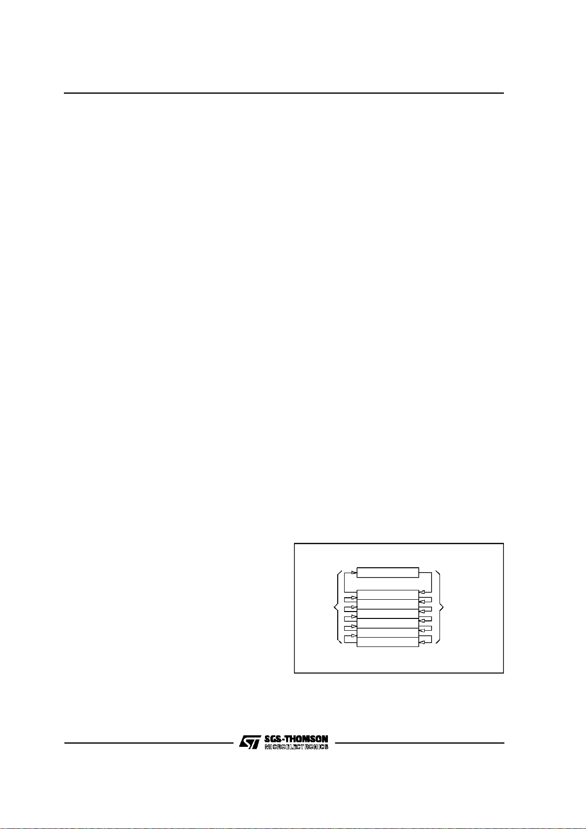
Figure1. ST6369 Pin Configuration GENERAL DESCRIPTION
The ST6369 microcontroller is member of the 8-bit
HCMOSST638xfamily,a seriesofdevicesspecially
orientedtoDigitalControlled MultiFrequencyMonitor applications. ST6369members are based on a
building block approach: a common core is surrounded by a combination of on-chip peripherals
(macrocells)availablefromastandardlibrary.These
peripheralsare designed with the same Core technology providing full compatibility and short design
time. Many of these macrocells are speciallydedicated to DCMF Monitor applications. The macrocellsof the ST6369 are: twoTimer peripheralseach
includingan 8-bitcounterwith a 7-bit software programmableprescaler(Timer), a digitalhardwareactivatedwatchdogfunction(DHWD), a 14-bitvoltage
synthesistuningperipheral,aSerialPeripheralInterface (SPI), six 6-bit PWM D/A converters, an A/D
converter with 0.5V resolution, a 14-bit PWM D/A
converter. In addition the following memory resources are available: program ROM (8K bytes),
dataRAM (256bytes),EEPROM (384bytes).
ST6369
2/67
Page 7
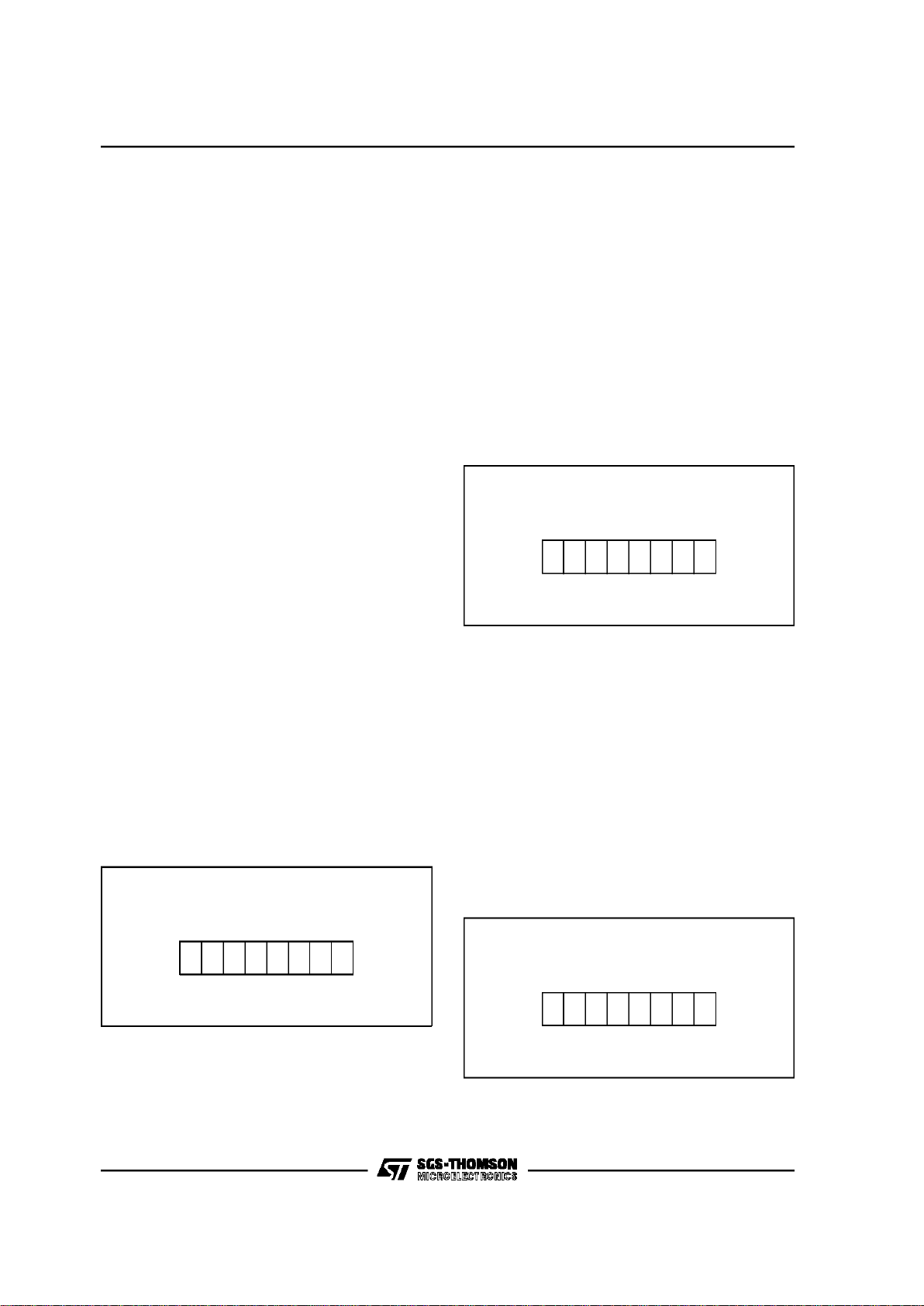
STACK LEVEL 1
STACK LEVEL 2
STACK LEVEL 3
STACK LEVEL 4
STACK LEVEL 5
STACK LEVEL 6
PC
D/AOutputs
TIMER 2
INTERRUPT
Inputs
TEST
TIMER 1
PORT C
PORT B
PORT A
A/D Input
DIGITAL
WATCHDOG/TIMER
SERIAL PERIPHE RAL
INTERFACE
V
DD
V
SS
OSCin OSCout
RESET
VR0B1 753
PA0 PA7 *
HDA,DA0 DA5
HSYNC/PC6
VSYNC
TEST
AD
PB0 PB7 *
PC2,PC4 PC7 *
PC0 / SCL
PC1 / SDA
PC3 / SEN
POWER SUPPLY OSCILLATOR RESET
8-BIT CORE
USER PROGRAM
ROM
8 kBytes
DATA ROM
USER SELECTABLE
DATA EEPROM
384 Bytes
DATA RAM
256 Bytes
* Refer To Pin Configuration For Additional Information
Figure2. ST6369 Block Diagram
DEVICE
ROM
(Bytes)
RAM
(Bytes)
EEPROM
(Bytes)
A/D
14-bit
D/A
6-bit
D/A
EMULATING
DEVICES
ST6369 8K 256 384 1 1 6 ST63E69, ST63T69
Table 1. Device Summary
ST6369
3/67
Page 8

PIN DESCRIPTION
V
DD
andVSS. Power issupplied to the MCU using
these twopins. V
DD
ispower and VSSistheground
connection.
OSCIN, OSCOUT. These pins are internally con-
nected to the on-chip oscillator circuit. A quartz
crystal or a ceramic resonator can be connected
between these two pins in order to allow the correct operation of the MCU with various stability/costtrade-offs. The OSCIN pin isthe input pin,
the OSCOUTpin is the output pin.
RESET. The activelow RESET pin is used to start
the microcontrollerto the beginning ofits program.
Additionally the quartz crystal oscillator will be disabled when theRESET pin islow to reduce power
consumption duringreset phase.
TEST. The TEST pin mustbe held at V
SS
for nor-
mal operation.
PA0-PA7. These 8 linesare organizedas oneI/O
port (A). Eachline may be configuredas either an
input withor withoutpull-upresistor or as an output
under softwarecontrol of the datadirectionregister. PinsPA4 toPA7 are configured as open-drain
outputs (12V drive). On PA4-PA7 pins the input
pull-up option is not available while PA6 and PA7
have additional current driving capability (25mA,
V
OL
:1V).PA0 to PA3pins areconfigured as push-
pull.
PB1-PB2, PB4-PB6. These 5 linesare organized
as one I/O port (B).Each line may be configuredas
either aninput withorwithoutinternalpull-up resistor or as an output under software control of the
data directionregister.
PC0-PC7. These 8 lines are organized as oneI/O
port (C). Each line may be configured as either an
input with or without internal pull-up resistoror as
an output under softwarecontrol of thedata direction register. Pins PC0 to PC3 are configured as
open-drain(5V drive)in output mode while PC4 to
PC7 are open-drain with 12V drive and the input
pull-up options does not exist on these four pins.
PC0, PC1 and PC3 lines when in output mode are
“ANDed” with the SPI control signals and are all
open-drain.PC0is connected to the SPI clock signal (SCL), PC1 with the SPI data signal (SDA)
while PC3 is connected with SPI enable signal
(SEN, used in S-BUSprotocol). Pin PC4 and PC6
can also be inputstosoftwareprogrammableedge
sensitive latches which can generate interrupts;
PC4 can be connected to Power Interrupt while
PC6 can be connected to the HSYNC/NMI interrupt line.
DA0-DA5. These pins are the six PWM D/A outputs of the 6-bit on-chip D/A converters. These
lines have open-drain outputs with 12V drive. The
output repetition rate is 31.25KHz (with 8MHz
clock).
AD. This is the input of the on-chip 10 levelscomparator that can be used to implement the Analog
Keyboard function. This pin is an highimpedance
input able to withstand signals with a peak amplitude upto 12V.
VSYNC. This is the Vertical Synchronization pin.
This pinis connected to an internal timer interrupt.
O0,O1. Thesetwo lines are outputopen-drain pins
with 12Vdrive.
HDA. This is the output pin of the on-chip 14-bit
PWMD/A Converter.This line isapush-pulloutput
with standarddrive.
ST6369
4/67
Page 9

Pin Function Description
DA0 to DA5 Output, Open-Drain, 12V
AD Input,High Impedance, 12V
HDA Output, Push-Pull
VSYNC Input, Pull-up, Schmitt Trigger
TEST Input, Pull-Down
OSCIN Input, Resistive Bias,Schmitt Triggerto Reset Logic Only
OSCOUT Output,Push-Pull
RESET Input, Pull-up, Schmitt Trigger Input
PA0-PA3 I/O, Push-Pull, Software Input Pull-up, Schmitt Trigger Input
PA4-PA5 I/O, Open-Drain, 12V,No Input Pull-up, Schmitt Trigger Input
PA6-PA7 I/O, Open-Drain, 12V,No Input Pull-up, Schmitt Trigger Input, High Drive
PB1-PB2 I/O, Push-Pull, Software Input Pull-up, Schmitt Trigger Input
PB4-PB6 I/O, Push-Pull, Software Input Pull-up, Schmitt Trigger Input
PC0-PC3 I/O, Open-Drain,5V , SoftwareInput Pull-up,Schmitt Trigger Input
PC4-PC7 I/O, Open-Drain,12V, No Input Pull-up, Schmitt Trigger Input
O0, O1 Output, Open-Drain, 12V
V
DD,VSS
Power Supply Pins
Table 2. Pin Summary
ST6369
5/67
Page 10
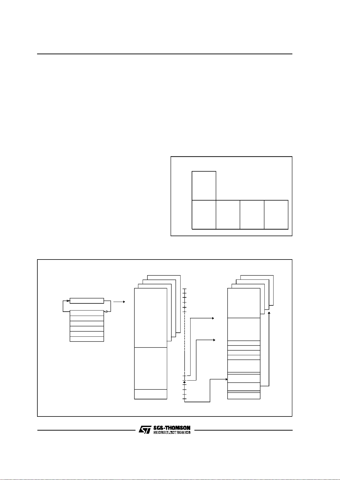
ST6369 CORE
The Core of the ST6369 is implemented independently from the I/O or memory configuration.
Consequently,it can betreatedas an independent
centralprocessorcommunicatingwithI/Oandmemoryvia internaladdresses,data,andcontrolbusses.
The in-core communication is arranged as shown
in the followingblock diagram figure; the controller
being externallylinkedto both thereset and the oscillator, while the core is linked to thededicatedonchip macrocells peripherals via the serial data bus
and indirectly for interrupt purposes through the
control registers.
Registers
The ST6369 Core has five registers and three
pairs of flags available to the programmer. They
are shown in Figure 4 and are explainedin the following paragraphstogether with the program and
data memorypage registers.
Accumulator (A). The accumulator is an 8-bit
general purpose register used in all arithmeticcalculations, logical operations, and data manipulations. The accumulator is addressed in the data
space asRAM locationat the FFH address.
Accordingly, the ST6369 instruction set can use
the accumulatoras anyother register of the data
space.
Figure3. Core Block Diagram
SHORT
DIRECT
ADDRESSING
MODE
V REGISTER
W REGISTER
PROGRAMCOUNTER
SIX LEVELS
STACKREGISTER
C
C
C
Z
Z
Z
NORMAL FLAGS
INTERRUPT FLAGS
NMI FLAGS
INDEX
REGISTER
VA000423
b7
b7
b7
b7
b7
b0
b0
b0
b0
b0
b0b11
ACCUMULATOR
Y REG. POINTER
X REG. POINTER
Figure4. Core ProgrammingModel
ST6369
6/67
Page 11
ST6369 CORE(Continued)
Indirect Registers (X, Y). These two indirect reg-
istersare usedas pointers tothe memorylocations
in the dataspace. They are usedin theregister-indirect addressing mode.These registers can be
addressed in the data space as RAM locations at
the 80H(X)and 81H (Y) addresses.They can also
be accessed with the direct, short direct, or bit direct addressing modes. Accordingly, the ST638x
instructionsetcan use the indirect registers as any
other registerof the data space.
Short Direct Registers (V, W). These two registers are used to save one byte in short direct addressing mode.These registerscan be addressed
in the data spaceas RAM locationsat the82H (V)
and 83H (W) addresses. They can also be accessed with the direct and bit direct addressing
modes. Accordingly, the ST638x instruction set
can use the shortdirect registers as any other register ofthe data space.
Program Counter (PC)
The program counter is a 12-bit registerthat contains the address of the next ROM location to be
processed by thecore.This ROM locationmay be
an opcode, an operand, or an address ofoperand.
The 12-bit length allows the direct addressing of
4096 bytes in the program space. Nevertheless, if
the program space contains more than 4096 locations, thefurtherprogram spacecan be addressed
by using theProgramROMPage Register.The PC
value isincremented,after it is read forthe address
of the current instruction,by sendingit through the
ALU, so giving the address of the nextbyte in the
program.Toexecuterelativejumpsthe PCand the
offset values are shifted through the ALU, where
they will be added, and the result is shifted back
into the PC. The program countercan be changed
in thefollowingways:
JP (Jump)instruction....PC=Jump address
CALL instruction...........PC=Call address
Relative Branch
instructions...................PC=PC+offset
Interrupt........................PC=Interruptvector
Reset............................PC=Resetvector
RET &RETI instructions............PC=Pop (stack)
Normal instruction........PC=PC+1
WHEN CALL
OR
INTERRUPT REQUEST
OCCURS
STACK LEVEL 1
STACK LEVEL 2
STACK LEVEL 3
STACK LEVEL 4
STACK LEVEL 5
STACK LEVEL 6
PROGRAM COUNTER
WHEN
RET OR RETI
OCCURS
VA000424
Figure5. Stack Operation
Flags (C, Z)
The ST6369 Core includesthree pairsof flagsthat
correspondto 3 different modes:normalmode,interrupt mode and Non-Maskable-Interrupt-Mode.
Each pair consistsof a CARRY flag and a ZERO
flag. One pair (CN, ZN) is used duringnormal operation, one pair is used during the interruptmode
(CI,ZI)andone is usedduring thenot-maskableinterruptmode (CNMI, ZNMI).
The ST6369 Core uses the pair of flags that correspondsto the actualmode: as soon as an interrupt
(resp. a Non-Maskable-Interrupt) is generated,the
ST6369Core uses the interruptflags(resp.the NMI
flags)insteadofthenormalflags.Whenthe RETIinstructionis executed,the normalflags(resp.the interrupt flags) are restored if the MCU was in the
normalmode (resp.inthe interruptmode)beforethe
interrupt.Shouldbe observedthateach flag setcan
onlybe addressedin itsownroutine(Not-maskable
interrupt,normalinterruptormainroutine).Theinterruptflags arenot clearedduring the contextswitchingand so,they remainin thestatethey were at the
exitof the lastroutineswitching.
The Carry flag is set when a carry or a borrow occurs during arithmetic operations, otherwise it is
cleared. The Carry flag is also set to the value of
the bit tested in a bit test instruction, and participates in the rotate left instruction.
TheZeroflagissetif theresultofthelastarithmetic
or logical operation wasequal to zero, otherwise it
is cleared.
The switching between these three sets is automaticallyperformedwhen anNMI,an interrupt and
a RETI instructions occur. As the NMI mode is
automatically selected after the reset ofthe MCU,
the ST6369Core uses at first the NMI flags.
ST6369
7/67
Page 12
ST6369 CORE (Continued)
Stack
The ST6369 Core includes true LIFO hardware
stack that eliminates the need fora stack pointer.
The stackconsists ofsixseparate12-bit RAMlocations that do not belong to the data space RAM
area. When a subroutine call (or interruptrequest)
occurs,the contentsofeach levelis shiftedinto the
next levelwhile the contentofthe PC is shiftedinto
the first level (the value of the sixth level will be
lost). When subroutine or interrupt return occurs
(RET or RETI instructions), the first levelregisteris
shifted back into the PCand thevalue of eachlevel
is shifted back into the previous level. These two
operating modes are describedin Figure 5. Since
the accumulator,as all otherdata space registers,
is notstored inthisstack the handling of thisregisters shall be performed inside the subroutine. The
stack pointer will remain in its deepest position,if
more than 6 calls or interrupts are executed, so
that the last return address will be lost. It will also
remain in its highest position if the stack is empty
and a RET or RETI is executed. In this case the
next instructionwill be executed.
Memory Registers
The PRPR can be addressed like a RAM location
in the Data Spaceat the CAH address; nevertheless it is a write-only register that can not be accessed with single-bit operations.This register is
used to select the 2-Kbyte ROM bank of the Program Spacethat will be addressed.The number of
the pagehastobe loaded inthePRPR.ThePRPR
is not cleared during the MCU initialization and
should thereforebe defined before jumpingout of
the static page. Refer to the Program Space description for additional information concerning the
use of this register. The PRPR is not modified
when an interruptor a subroutine occurs.
PRPR
Program ROMPage Register
(CAH, Write Only)
D7 D6 D5 D4 D3 D2 D1 D0
Figure6. Program ROMPage Register
DRBR
Data RAM Bank Register
(E8H, Write Only)
D7 D6 D5 D4 D3 D2 D1 D0
Figure7. Data RAM Bank Register
DRWR
Data ROM Window Register
(C9H, Write Only)
D7 D6 D5 D4 D3 D2 D1 D0
Figure8. Data ROM WindowRegister
The DRBR can be addressedlike a RAMlocation
in the Data Space at the E8H address, nevertheless it is write-only register that can not be accessed with single-bit operations. This register is
used to select the desired 64-byteRAM/EEPROM
bank of the Data Space. The numberof the bank
has to be loaded inthe DRBR and the instruction
has to point to the selected location as itwas inthe
0 bank (from 00H address to 3FH address). This
register is undefined afterReset. Refer to the Data
Space description for additional information. The
DRBR register is not modified when a interrupt or
a subroutine occurs.
TheDRWR registercanbeaddressedlike a RAMlocationintheDataSpaceattheC9Haddress,nevertheless it is write-only register that can not be
accessed with single-bit operations.This registeris
used to move up and down the 64-byte read-only
datawindow(from the 40H address to 7FHaddress
of the Data Space)along the ROM of the MCU by
stepof 64 bytes.Theeffectiveaddressof thebyteto
bereadasadata inthe ROMisobtainedbythe concatenationofthe6lesssignificantbitsoftheaddress
given in the instruction(as less significant bits)and
the content of the DRWR (as most significant
bits). Refer to the Data Space descriptionfor additionalinformation.
ST6369
8/67
Page 13
MEMORY SPACES
The MCUs operate in three different memory
spaces: Stack Space, Program Space and Data
Space. A descriptionof these spaces is shown in
Figure 9.
Stack Space
Thestack spaceconsistsof six 12 bit registers that
areusedfor stackingsubroutineandinterrupt return
addressesplusthecurrentprogramcounterregister.
Program Space
The program space is physically implemented in
the ROM and includes all the instructionsthat are
to be executed, as well as the data requiredforthe
immediate addressing mode instructions, the reserved test area and uservectors. It is addressed
thanks to the 12-bit Program Counter register (PC
register) and so, the ST6369 Core can directlyaddress up to 4Kbytesof ProgramSpace.Nevertheless, the Program Space can be extended by
the addition of 2-KbyteROM banks as it is shown
in Figure 11 in which a 8K bytes memory is described.Thesebanks areaddressed bypointing to
the 000H-7FFH locations of the Program Space
thanks to the Program Counter, andby writingthe
appropriatecode in theProgram ROM Page Register (PRPR) located at the CAH address of the
Data Space.Becauseinterruptsand common sub-
PROGRAM SPACE
VR001568
INTERRUPT &
RESET VECTORS
ACCUMULATOR
WREGISTER
RAM
DATA ROM
WINDOW
RAM / EEPROM
BANKING AREA
DATA SPACE
DATA RAM
BANK SELECT
DATA ROM
WINDOW SELECT
VREGISTER
YREGISTER
XREGISTER
0-63
0000h
07FFh
0800h
0FF0h
0FFFh
000h
03Fh
040h
070h
080h
081h
082h
083h
084h
0FFh
0C0h
ROM
ROM
STACK LEVE L 1
STACK LEVE L 2
STACK LEVE L 3
STACK LEVE L 4
STACK LEVE L 5
STACK LEVE L 6
PROGRAM COUNTER
STACK SPACE
Figure9. Memory Addressing Description Diagram
routines should be availableall the time only the
lower 2K byte of the 4K programspace are bank
switched while the upper 2K byte can be seen as
static space. Table 3 gives thedifferent codes that
allows the selection of the corresponding banks.
Note that,fromthe memory point of view,thePage
1 and the StaticPage represent the same physical
memory:it isonly adifferentway ofaddressingthe
same location.
Program
counter
space
0000H 1FFFH
0FFFH
Static Page
Page 1
0800H
07FFH
Page 0
Page 1
Static Page
Page 2 Page 3
0000H
Figure10. 8K Bytes Program Space Addressing Description
ST6369
9/67
Page 14
D7-D2.Thesebitsare not used but haveto bewritten to “0”.
PRPR1-PRPR0. These are the program ROM
banking bits and thevalue loaded selects the corresponding page to be addressedin the lower part
of 4Kprogramaddress spaceas specifiedin Table
3. Thisregisteris undefined onreset.
MEMORY SPACES(Continued)
Note. Only the lower part of address space has
been bankswitchedbecause interrupt vectors and
common subroutines should be available all the
time. The reason of this structureis dueto the fact
that it isnot possible to jumpfrom a dynamicpage
to another,unlessjumping back to the staticpage,
changingcontents of PRPR,and, then, jumping to
a differentdynamicpage.
Care is required when handlingthe PRPR as it is
write only. For this reason, it is not allowed to
change the PRPR contents while executing interrupts drivers, as the driver cannot save and than
restore its previous content. Anyway, this operation may be necessary if thesum ofcommon routines and interrupt driverswill take more than 2K
bytes; in this case could benecessaryto divide the
interrupt driver in a (minor) part in the static page
(start and end), and in the second (major) part in
one dynamic page. If it is impossible to avoid the
writing of this register in interrupts drivers, an image of this register must be saved in a RAMlocation, and eachtime theprogramwrites the PRPRit
writes also the image register.The image register
must be written first, so if an interruptoccurs between the two instructions the PRPR is not affected.
PRPR
Program ROMPage Register
(CAH, Write Only)
D7 D6 D5 D4 D3 D2 D1 D0
PRPR0
PRPR1
UNUSED
UNUSED
UNUSED
Figure11. Program ROM Page Register
PRPR1 PRPR0 PC11
Memory
Page
X X 1 StaticPage (Page 1)
0 0 0 Page0
010
Page 1
(Static Page)
1 0 0 Page2
1 1 0 Page3
Table 3. Program ROM Page RegisterCoding
ROM Page Device Address Description
PAGE 0
0000H-007FH
0080H-07FFH
Reserved
User ROM
PAGE 1
“STATIC”
0800H-0F9FH
0FA0H-0FEFH
0FF0H-0FF7H
0FF8H-0FFBH
0FFCH-0FFDH
0FFEH-0FFFH
User ROM
Reserved
Interrupt Vectors
Reserved
NMI Vector
Reset Vector
PAGE 2
0000H-000FH
0010H-07FFH
Reserved
User ROM
PAGE 3
0000H-000FH
0010H-07FFH
Reserved
User ROM
Table 4. ST6369 Program ROM Map
ST6369
10/67
Page 15
MEMORY SPACES(Continued)
b7 b0
000H
DATARAM/EEPROM
BANK AREA
03FH
040H
DATA ROM
WINDOW AREA
07FH
X REGISTER 080H
Y REGISTER 081H
V REGISTER 082H
W REGISTER 083H
084H
DATA RAM
0BFH
PORT A DATA REGISTER 0C0H
PORT B DATA REGISTER 0C1H
PORT C DATAREGISTER 0C2H
RESERVED 0C3H
PORT ADIRECTION REGISTER 0C4H
PORT BDIRECTION REGISTER 0C5H
PORT CDIRECTION REGISTER 0C6H
RESERVED 0C7H
INTERRUPT OPTION REGISTER 0C8H
DATA ROM WINDOW REGISTER 0C9H
PROGRAM ROM PAGE REGISTER 0CAH
RESERVED 0CBH
SPI DATAREGISTER 0CCH
0CDH
RESERVED
0D1H
TIMER 1PRESCALER REGISTER 0D2H
TIMER 1 COUNTER REGISTER 0D3H
TIMER1 STATUS/CONTROL REG. 0D4H
0D5H
RESERVED
0D7H
WATCHDOG REGISTER 0D8H
Figure12. Data Space
b7 b0
RESERVED 0D9H
TIMER 2 PRESCALER REGISTER 0DAH
TIMER2 COUNTER REGISTER 0DBH
TIMER 2STATUSCONTROL REG. 0DCH
0DDH
RESERVED
0DFH
DA0 DATA/CONTROL REGISTER 0E0H
DA1 DATA/CONTROL REGISTER 0E1H
DA2 DATA/CONTROL REGISTER 0E2H
DA3 DATA/CONTROL REGISTER 0E3H
AD, HSYNC RESULT REGISTER 0E4H
OUTPUTS CONTROL REGISTER 0E5H
DA4 DATA/CONTROL REGISTER 0E6H
DA5 DATA/CONTROL REGISTER 0E7H
DATA RAM BANK REGISTER 0E8H
DEDIC. LATCHES CONTROL REG. 0E9H
EEPROMCONTROL REGISTER 0EAH
SPICONTROL REGISTER 1 0EBH
SPICONTROL REGISTER 2 0ECH
RESERVED 0EDH
HDA DATA REGISTER 1 0EEH
HDA DATA REGISTER 2 0EFH
0F0H
RESERVED
0FEH
ACCUMULATOR 0FFH
Figure13. Data Space (Continued)
Data Space
The instruction set of the ST6369Core operates
on a specific space, named Data Space thatcontains all the data necessaryfor the processing of
the program. The Data Space allows the ad-
dressing of RAM (256 bytes), EEPROM (384
bytes), ST6369 Core/peripheral registers, and
read-only data such as constants and the look-up
tables.
ST6369
11/67
Page 16

MEMORY SPACES(Continued)
Data ROMAddressing.All theread-onlydata are
physically implemented in the ROM in which the
Program Space is also implemented. The ROM
thereforecontains theprogram to be executedand
also the constants and thelook-up tablesneeded
for the program. The locations of Data Space in
which the different constants and look-up tables
are addressedby the ST6369 Core can beconsidered asbeing a 64-bytewindow through which it is
possible to access to the read-only data stored in
the ROM.This window is located from the 40Haddress to the 7FHaddress in theData spaceandallows the direct reading of the bytes from the 000H
address to the 03FH address in the ROM. All the
bytes of the ROMcan be used to store either instructions or read-only data. Indeed, the window
can be moved by step of 64bytes along the ROM
in writing the appropriate code in the Write-only
Data ROM Window register (DRWR, location
C9H). The effectiveaddress of the byte to be read
as a datainthe ROMisobtained bytheconcatenation of the 6 less significant bits of the address in
the Data Space (as less significant bits) and the
content ofthe DRWR(as mostsignificant bits). So
when addressing location 40H of data space, and
0 is loaded in the DRWR, the physicaladdressed
location in ROM is 00H.
DWR6-DWR0. These are the Data Rom Window
bits that correspond to the upper bits ofdata ROM
program space. This registeris undefinedafter reset.
Note.CareisrequiredwhenhandlingtheDRWR as
it is write only. For this reason, it is not allowed to
change the DRWR contents while executing interruptsdrivers, as thedrivercannotsaveand thanrestoreits previouscontent.If it is impossibleto avoid
thewriting ofthisregisterininterruptsdrivers, animageofthisregistermustbe savedinaRAMlocation,
and each time the program writes the DRWR it
writes also the image register. The image register
must be written first, so if an interrupt occurs betweenthe two instructionsthe DRWRregister is not
affected.
DWR
Data ROMWindow Register
(C9H, Write Only)
D7 D6 D5 D4 D3 D2 D1 D0
DWR0 = Data ROMWindow 0
DWR1 = Data ROMWindow 1
DWR2 = Data ROMWindow 2
DWR3 = Data ROMWindow 3
DWR4 = Data ROMWindow 4
DWR5 = Data ROMWindow 5
DWR6 = Data ROMWindow 6
UNUSED
Figure14. Data ROM Window Register
DATA ROM
WINDOW REGISTER
CONTENTS
DATA SPACE ADDRESS
40h-7Fh
IN INSTRUCTION
PROGRAM SPACE ADDRESS
65432 0
543210
543210
READ
1
67891011
0
1
VR01573B
12
1
0
DATA SPACE ADDRESS
59h
0000
0
1
00
1
11
Example:
(DWR)
DWR=28h
11000000001
ROM
ADDRESS:A19h
11
13
01
7
0
0
Figure15. Data ROM Window Memory Addressing
ST6369
12/67
Page 17
DRBR
Data RAM
Bank Register
(E8H, Write Only)
D7 D6 D5 D4 D3 D2 D1 D0
DRBR0
DRBR1
DRBR2
DRBR3
DRBR4
DRBR5
DRBR6
DRBR7
Figure16. Data RAM Bank Register
MEMORY SPACES(Continued)
Data RAM/EEPROM
IntheST636964 bytesofdataRAM are directlyaddressable in the data space from 80H to BFH addresses.Theadditional192 bytesof RAM, the 384
bytes of EEPROM can be addressed using the
banks of64 byteslocated between addresses 00H
and 3FH. The selection of the bank is done by programming the Data RAM Bank Register (DRBR)
located at the E8H address of the Data Space. In
this way each bank of RAM, EEPROM can select
64 bytes at a time. No more than one bank should
be set at a time.
DRBR7,DRBR1,DRBR0. These bits select the
EEPROM pages.
DRBR4,DRBR3,DRBR2.Each of these bits,when
set,will select one RAM page.
This registeris undefined afterreset.
Table 5 summarizes how to set the Data RAM
Bank Register in order to select the various banks
or pages.
Note :
Care is required when handling the DRBR asit is
write only. For this reason, it is not allowed to
change the DRBR contentswhile executing interrupts drivers, as the driver cannot save and than
restore its previous content. If it is impossible to
avoid the writing of this register in interrupts drivers, an image of this register must be saved in a
RAM location, and each time the program writes
the DRBRit writes also the image register.
The image registermustbe written first,so if an interrupt occurs between the two instructions the
DRBR is not affected.
EEPROMDescription
The data space ofST6369 family from00H to3FH
is paged as described in Table 5. 384 bytes of
EEPROMlocated in six pages of 64 bytes(pages
0,1,2,3,4and 5, see Table 5).
DRBR Value
Selection
Hex. Binary
01H 0000 0001 EEPROM Page0
02H 0000 0010 EEPROM Page1
03H 0000 0011 EEPROM Page2
81H 1000 0001 EEPROM Page3
82H 1000 0010 EEPROM Page4
83H 1000 0011 EEPROM Page5
04H 0000 0100 RAM Page 2
08H 0000 1000 RAM Page 3
10H 0001 0000 RAM Page 4
Table 5. Data RAMBank Register Set-up
ST6369
13/67
Page 18
Through the programmingof the Data RAM Bank
Register (DRBR=E8H) the user can select the
bank or page leaving unaffected the way to address the static registers. The way to address the
“dynamic”page is tosetthe DRBRas described in
Table 5(e.g.to selectEEPROMpage 0,the DRBR
has to be loaded with content 01H, see Data
RAM/EEPROMaddressing for additional information). Bits 0, 1 and 7 ofthe DRBR are dedicated to
the EEPROM.
The EEPROM pages do not require dedicated instructions to be accessedin readingor writing.The
EEPROM is controlled by the EEPROM Control
Register(EECR=EAH). AnyEEPROM location can
bereadjust likeanyotherdatalocation,alsointerms
ofaccesstime.
To write an EEPROM location takes an average
time of 5 ms (10ms max) and during this timethe
EEPROM is not accessible by the Core. A busy
flag canbe readby the Coretoknow the EEPROM
status before trying any access. In writing the
EEPROM can work in two modes: Byte Mode
(BMODE) and Parallel Mode (PMODE).
The BMODE is the normal way to use the
EEPROMand consistsin accessingone byte at a
time. The PMODE consists in accessing 8 bytes
per time.
D7. Not used
SB. WRITEONLY. If thisbit isset the EEPROMis
disabled (any access will be meaningless) and
the power consumption of the EEPROM is reduced tothe leakage values.
D5, D4. Reserved for testingpurposes,they must
be setto zero.
PS.SET ONLY. Oncein Parallel Mode,assoon as
the user softwaresets the PS bit the parallel writing ofthe 8adjacent registerswill start.PS isinternally reset at the end of the programming
procedure.Note thatless than8 bytescan be written; after parallel programming the remaining undefined byteswill have no particularcontent.
PE. WRITE ONLY. This bit must be set by the
userprogram in orderto performparallel programming (more bytes per time). If PE is set and the
“parallelstartbit”(PS)is low, up to 8adjacentbytes
can be writtenat the maximum speed, the content
being storedin volatileregisters.These 8 adjacent
bytes can be considered as row, whose A7, A6,
A5, A4, A3 are fixed while A2, A1 and A0 are the
changing bytes. PE is automatically reset at the
end of any parallel programming procedure. PE
can be reset by the user software before starting
the programming procedure, leaving unchanged
the EEPROMregisters.
BS.READ ONLY. This bitwill be automaticallyset
by the CORE when the user program modifies an
EEPROMregister. The user program hasto test it
before any read or write EEPROM operation; any
attemptto accessthe EEPROMwhile “busy bit” is
setwillbeabortedandthewriting procedureinprogress completed.
EN. WRITE ONLY.This bit MUSTbe set to one in
order to write any EEPROM register. If the user
program will attempt to write the EEPROM when
EN= “0” the involved registers will be unaffected
and the”busy bit”will notbe set.
AfterRESE TthecontentofEECRregisterwillbe00H.
Notes :
When the EEPROM is busy (BS=”1”) the EECR
can notbe accessed inwrite mode, it is only possible to read BSstatus.This implies that as long as
the EEPROM is busy it is not possible to change
the status of the EEPROM control register. EECR
bits 4 and 5 are reserved for test purposes, and
must never be set to “1”.
Additional Notes on Parallel Mode. If the user
wants to perform a parallel programming the first
action should betheset to one the PEbit; fromthis
moment the first time the EEPROM will be addressed in writing, the ROW address will be
latched and it will be possibleto changeit only at
the endofthe programming procedureor by reset-
MEMORY SPACES(Continued)
EECR
EEPROM Control Register
(EAH, Read/Write)
D7 D6 D5 D4 D3 D2 D1 D0
EN = EEPROMEnable Bit
BS = EEPROM Busy Bit
PE = Parallel Mode Enable Bit
PS = Parallel Start Bit
Reserved (Mustbe set Low)
Reserved (Mustbe set Low)
SB =Stand-by Enable Bit
Unused
Figure17. EEPROM Control Register
ST6369
14/67
Page 19

ting PE without programming the EEPROM.After
the ROWaddress latching the Core can “see” just
one EEPROMrow (the selected one) and any attempt to write or read other rows will produceerrors. Donot read the EEPROMwhile PEis set.
As soon asPE bitis set,the 8volatile ROW latches
are cleared. From this moment the user can load
data in the whole ROW or just in a subset.PS setting willmodify theEEPROM registerscorresponding to the ROW latches accessed after PE. For
example, if the software sets PE and accesses
EEPROMinwritingataddresses18H,1AH,1BHand
thensetsPS,thesethreeregisterswill bemodifiedat
thesame time;the remainingbyteswill haveno particularcontent.NotethatPE isinternallyresetat the
endof theprogramming procedure.Thisimplies that
the user must set PE bit between two parallelprogrammingprocedures.Anywaytheusercansetand
thenresetPEwithoutperforminganyEEPROMprogramming.PS is a setonly bitand isinternallyreset
atthe end of the programmingprocedure.Notethat
if theusertriestosetPSwhilePEisnotsettherewill
not be any programming procedure and the PS bit
will be unaffected.ConsequentlyPS bitcan not be
setifENis low.PScanbeaffectedbythe usersetif,
andonlyif,ENand PE bits arealsosetto one.
MEMORY SPACES(Continued)
INTERRUPT
The ST6369 Core can manage 4 different maskable interrupt sources, plus one non-maskable interrupt source (top priority level interrupt). Each
sourceisassociated with aparticularinterruptvector that contains a Jump instruction to the related
interrupt serviceroutine. Each vector is located in
the Program Space at a particular address (see
Table 6). When a source provides an interruptrequest, and therequest processingis alsoenabled
by theST6369 Core,then thePC registerisloaded
with the address of the interrupt vector (i.e.of the
Jumpinstruction).Finally,the PC isloaded withthe
address of the Jump instruction and the interrupt
routine is processed.
The relationship between vector and source and
the associatedpriority ishardware fixed for the differentST638xdevices. Forsome interrupt sources
it is also possible to select by software the kind of
event that will generatethe interrupt.
All interruptscan be disabled by writingto theGEN
bit (global interruptenable) of the interrupt option
register (address C8H). After a reset, ST6369 is in
non maskable interruptmode, so no interrupts will
be accepted and NMI flags will be used, until a
RETI instruction is executed.If an interruptis executed, one special cycle is made by the core,during that the PC is set to the related interrupt vector
address. A jump instructionat thisaddress has to
redirect program execution to thebeginningof the
relatedinterruptroutine.Theinterruptdetectingcycle, also resets the relatedinterrupt flag(not available to the user), so that another interrupt can be
stored for this current vector, while its driver is under execution.
If additionalinterruptsarrivefromthe same source,
they will be lost. NMI can interrupt other interrupt
routines at any time,while other interrupts cannot
interrupt each other. If more than one interrupt is
waiting forservice, they are executed according to
their priority. The lower the number, the higher the
priority. Priority is, therefore, fixed. Interrupts are
checked during the last cycle of an instruction
(RETIincluded). Level sensitive interrupts have to
be validduring this period.
Table 6 details the different interrupt vectors/sourcesrelationships.
InterruptVectors/Sources
The ST6369 Core includes 5 different interrupt
vectors in order to branch to 5 different interrupt
routines. The interrupt vectors are located in the
fixed (or static)page ofthe ProgramSpace.
ST6369
15/67
Page 20
The interruptvectorassociatedwith thenon-maskable interrupt source is named interrupt vector#0.
It is located at the (FFCH,FFDH) addressesin the
Program Space.This vector is associatedwith the
PC6/IRINpin.
The interrupt vectors located at addresses
(FF6H,FF7H), (FF4H,FF5H), (FF2H,FF3H),
(FF0H,FF1H) are named interrupt vectors #1, #2,
#3 and #4respectively.These vectorsare associated with TIMER 2 (#1), VSYNC (#2), TIMER 1
(#3) and PC4(PWRIN)(#4).
InterruptPriority
The non-maskable interrupt request has the highest priority and can interrupt any other interrupt
routines at any time, nevertheless the other interrupts cannot interrupteach other. Ifmore than one
interrupt requestis pending,they areprocessedby
the ST6369 Core according to their priority level:
vector#1 has the higherprioritywhile vector#4the
lower. Thepriority of each interrupt sourceis hardware fixed.
InterruptOption Register
The Interrupt Option Register (IOR register, location C8H) is used to enable/disablethe individual
interrupt sources and to select the operating mode
of theexternal interrupt inputs.Thisregistercanbe
addressed in the Data Space as RAM location at
the C8H address, nevertheless it is write-only register that can not be accessed with single-bit operations. The operating modes of the external
interrupt inputs associated to interrupt vectors #1
and #2are selectedthrough bits4 and5 of theIOR
register.
D7. Not used.
EL1. This is the Edge/Level selection bit of inter-
rupt#1.When set to one,the interruptisgenerated
on low level of the related signal; when cleared to
zero,the interruptisgenerated on falling edge.The
bit iscleared to zero after reset.
ES2. This is the edge selection bit on interrupt#2.
ThisbitisusedontheST6369deviceswithon-chip
OSDgenerator for VSYNC detection.
GEN.Thisis theglobalenablebit.Whensetto oneall
interruptsaregloball yenabled;whe nthisbitis cleared
tozero all interruptsaredisabl ed(excludingNMI).
D3 - D0. Thesebits are not used.
Interrupt Source
Associated
Vector
Vector Address
PC6/IRIN
Pin (1)
Interrupt
Vector # 0 (NMI)
0FFCH-0FFDH
Timer 2
Interrupt
Vector # 1
0FF6H-0FF7H
Vsync
Interrupt
Vector # 2
0FF4H-0FF5H
Timer 1
Interrupt
Vector # 3
0FF2H-0FF3H
PC4/PWRIN
Interrupt
Vector # 4
0FF0H-0FF1H
Note: 1. This pin isassociated with the NMIInterrupt Vector
Table 6. Interrupt Vectors/Sources
Relationships
INTERRUPT(Continued)
IOR
InterruptOption Register
(C8H, Write Only)
D7 D6 D5 D4 D3 D2 D1 D0
Unused
GEN = Global EnableBit
ES2 = Edge SelectionBit
EL1 = EdgeLevelSelection Bit
Unused
Unused
GEN = Global EnableBit
ES2 = Edge SelectionBit
EL1 = EdgeLevelSelection Bit
Unused
Figure18. InterruptOption Register
ST6369
16/67
Page 21

InterruptProcedure
The interruptprocedure is verysimilar to a callprocedure; the user can consider the interruptas an
asynchronous call procedure. As this is an asynchronous event the user does notknow about the
context and thetime at which itoccurred. As a result the user should save all the data space registers whichwill be usedinsidetheinterruptroutines.
There are separatesets of processor flags for normal, interrupt and non-maskable interrupt modes
which are automaticallyswitched and so these do
not need to be saved.
The following list summarizes the interruptprocedure (refer also to Figure 19. InterruptProcessing
Flow Chart):
-
Interrupt detection
-
The flags C and Z of the main routine are exchanged with the flags C and Z of the interrupt
routine (resp.the NMIflags)
-
The valueof thePC is storedin the firstlevel of
the stack- The normalinterrupt lines are inhibited (NMI still active)
-
The edgeflip-flop is reset
-
The relatedinterrupt vectoris loaded inthe PC.
-
User selected registers are saved insidethe interrupt service routine (normally on a software
stack)
-
The source of the interrupt is found by polling
(if more than one source is associated to the
same vector)
-
Interrupt servicing
-
Return from interrupt (RETI)
-
Automatically the ST63xx core switches back
to the normal flags (resp the interrupt flags)
and pops the previous PC value from the stack
The interruptroutine begins usually by the identification of the device that has generated the interrupt request. The user should save the registers
which are used inside the interrupt routine (that
holds relevantdata) intoa software stack.
Afterthe RETIinstruction execution,the Core carries out theprevious actions and the main routine
can continue.
ST6369 Interrupt Details
IR Interrupt (#0). The IRIN/PC6 Interrupt is con-
nected to the firstinterrupt#0 (NMI, 0FFCH).If the
IRINT interrupt is disabled at the Latch circuitry,
then it will be high. The #0 interrupt input detectsa
high to low level. Note that once #0 has been
latched, then the only way to remove the
latched #0 signal is to service the interrupt. #0
can interrupt the other interrupts. A simple latch
is provided from the PC6(IRIN) pin in order to
generate the IRINT signal. This latch can be triggered by either the positive or negative edge of
IRIN signal. IRINT is inverted with respect to the
latch. The latch can be read by software and reset bysoftware.
INTERRUPT(Continued)
LOAD PC FROM
INTERRUPT VECTOR
( FF C / FFD )
SET
INTERRUPT MASK
PUSH THE
PC INTO THE STACK
SELECT
INTERNAL MODE FLAG
CHECK IF THERE IS
AN INTERRUPT REQUEST
AND INTERRUPT MASK
INSTRUCTION
WAS
THE INSTRUCTION
ARETI
IS THE CORE
ALREADY IN
NORMAL MODE ?
FETCH
INSTRUCTION
EXECUTE
INSTRUCTION
CLEAR
INTERRUPT MASK
SELECT
PROGRAM FLAGS
” POP ”
THE STACKED PC
NO
NO
YES
YES
?
?
NO
YES
VA000014
Figure19. InterruptProcessingFlow-Chart
ST6369
17/67
Page 22

INTERRUPT(Continued)
TIMER 2 Interrupt (#1). The TIMER 2 Interrupt is
connectedto theinterrupt#1(0FF6H). TheTIMER2
interrupt generatesa low level (which is latchedin
thetimer). Onlythelowlevelselection for#1 can be
used.Bit6 of theinterrupt opti onregi ster C8 Hhasto
beset.
VSYNC Interrupt (#2). The VSYNC Interrupt is
connected to the interrupt #2. When disabled the
VSYNC INT signal is low. The VSYNC INT signal
is invertedwith respect to the signal appliedto the
VSYNC pin. Bit 5 of the interrupt option register
C8H is used to selectthe negative edge (ES2=0)
or the positive edge (ES2=1); the edge will depend on theapplication. Note thatonce an edge
has been latched, then the only way to remove
the latchedsignal is to service the interrupt.Care
must be taken not to generate spurious interrupts. This interruptmay be used for synchronize
to the VSYNCsignalin order to change characters
in the OSD only when the screen is on vertical
blanking (if desired). This method may also be
used toblink characters.
TIMER 1 Interrupt(#3). The TIMER 1 Interruptis
connected to the fourthinterrupt#3 (0FF2H)which
detectsa low level(latched in the timer).
PWR Interrupt (#4). The PWR Interrupt is connected to the fifth interrupt #4 (0FF0H). If the
PWRINT is disabled at the PWR circuitry, then it
will be high. The #4 interrupt input detects a low
level. A simple latch is provided from the PC4
(PWRIN)pinin order to generate the PWRINT signal. This latch can be triggered by either thepositive or negative edge of the PWRIN signal.
PWRINT is inverted with respectto the latch. The
latch can be resetby software.
Notes Global disable does not reset edge sensitive interruptflags. These edge sensitive interrupts
becomependingagainwhenglobaldisablingis released. Moreover, edge sensitive interrupts are
stored in therelated flags also when interrupts are
globallydisabled,unlesseachedge sensitiveinterrupt is also individually disabled before the interrupting event happens. Global disable is done by
clearing the GEN bit of Interrupt option register,
while any individual disable is done in the control
register of the peripheral. The on-chip Timer peripheralshavean interruptrequestflagbit(TMZ ), this
bit isset to one when thedevicewantstogeneratean
interruptrequestandama skbit(ETI)thatmustbeset
tooneto allowthe transferof the flagbit totheCore.
ST6369
18/67
Page 23

VA000200
TO ST6
RESET
ST6
INTERNAL RESET
OSCILLATOR
SIGNAL
WATCHDOG RESET
V
DD
300k
RESET
(ACTIVE LOW)
COUNTER
1.0k
Figure20. Internal Reset Circuit
RESET
The ST6369 devices can be resetin twoways: by
theexternalresetinput(RESET)tied low and by the
hardwareactivateddigitalwatchdogperipheral.
RESETInput
Theexternalactivelow reset pin isusedtoresetthe
ST6369 devices and provide an orderly software
startup procedure. The activation of the Reset pin
may occur at any time in the RUNor WAIT mode.
Even short pulsesat the reset pin will be accepted
sincethe resetsignalis latchedinternallyandisonly
cleared after 2048 clocks at the oscillatorpin. The
clocks from the oscillator pin to the reset circuitry
are bufferedbya schmitttriggersothatan oscillator
in start-up conditions will not give spurious clocks.
When the reset pin is held low, the external crystal
oscillatoris also disabledin order to reducecurrent
consumption. The MCU is configured in the Reset
modeas longas the signalofthe RESET pinis low.
The processing of the program is stoppedand the
standardInput/Outputports (portA, port B and port
C) are inthe inputstate.As soonas the levelon the
resetpinbecomeshigh,theinitializationsequenceis
executed.Refer to the MCU initialization sequence
foradditionalinformation.
WatchdogReset
The ST6369 devicesare provided withan on-chip
hardware activateddigital watchdogfunction inorder to providea graceful recovery from a software
upset.Ifthe watchdog registeris not refreshed and
the end-of-count is reached, then the reset state
will be latched into the MCU andan internalcircuit
pulls down the reset pin. This also resets the
watchdog which subsequently turns off the pulldown and activates thepull-up device at thereset
pin. This causes the positivetransition at the reset
pin. The MCU will then exit the reset state after
2048 clockson the oscillator pin.
ApplicationNotes
Anexternalresistorbetween V
DD
and theresetpin
is not requiredbecausean internal pull-up device
is provided.Theusermay prefer to addan external
pull-up resistor.
An internal Power-on device does notguarantee
that the MCU will exit the reset state when V
DD
is
above 4.5V and therefore the RESET pin should
be externallycontrolled.
ST6369
19/67
Page 24

RESET
IS RESET
STILL PRESENT ?
YES
NO
VA000427
NMI MASK SET
INT LATCH CLEARED
( IF PRESENT )
SELECT
NMI MODE FLAGS
PUT FFEh
ON ADDRESS BUS
LOAD PC
FROM RESET LOCATIONS
FFE / FFF
FETCH INSTRUCTION
Figure21. Reset & Interrupt Processing
Flow-Chart
JP
RESET VECTOR
INITIALIZATION
ROUTINE
JP: 2 BYTES/4 CYCLES
RETI: 1BYTES/2 CYCLES
RETI
VA000181
RESET
Figure22. Restart InitializationProgram
Flow-Chart
MCU InitializationSequence
When a reset occurs the stackis resetto program
counter, the PC is loaded with the addressof the
reset vector (located in the program ROM at addresses FFEH & FFFH). A jump instruction to the
beginning of the program has to be written into
these locations.After a resetthe interruptmask is
automatically activated so that the Coreis in nonmaskable interruptmode to prevent false or ghost
interrupts during the restartphase. Therefore the
restart routine should be terminatedby a RETIinstruction to switch to normalmode and enable interrupts. If no pending interrupt is present at the
end of the reset routine, the ST6369 will continue
with the instruction after the RETI; otherwise the
pendinginterrupt will be serviced.
RESETLow Power Mode
When the reset pin is low, the quartz oscillator is
Disabled allowing reduced current consumption.
When the reset pin is raisedthe quartzoscillator is
enabled and oscillations will start to build up.The
internal resetcircuitrywill count 2048clocks on the
oscillator pin before allowingthe MCUto go out of
the resetstate;theclocks areafter a schmitttrigger
so thatfalse or multiple counts arenot possible.
RESET(Continued)
ST6369
20/67
Page 25

WAIT & STOPMODES
The STOP and WAIT modes have been implemented in the ST6369 Core inorder toreduce the
consumption of the device when the latter has no
instruction to execute. These two modes are described in the following paragraphs.On ST6369 as
the hardwareactivateddigital watchdog functionis
present the STOPinstruction is de-activated and
any attempt to execute it will cause the automatic
execution ofa WAIT instruction.
WAIT Mode
Theconfigurationofthe MCUintheWAITmodeoccurs as soon as the WAIT instruction is executed.
Themicrocontrollercan alsobeconsideredasbeing
in a “software frozen” state where the Core stops
processing the instructions of the routine, the contents of the RAM locationsand peripheralregisters
are saved as long as the power supply voltage is
higherthantheRAMretentionvoltagebutwherethe
peripheralsarestill working.
The WAIT mode is used when the user wants to
reduce the consumptionof the MCU when it is in
idle, while not losing count of timeor monitoring of
external events. The oscillator is not stopped in
order to provide clock signal to the peripherals.
The timers counting may be enabled (writing the
PSI bit in TSCR register) and the timer interrupt
may be also enabled before entering the WAIT
mode; this allows the WAIT mode to be left when
timer interrupt occurs. If the exit from the WAIT
mode is performed with a general RESET (either
from the activation of the external pin or by watchdog reset) the MCUwill enter a normal reset procedure as described in the RESETchapter. If an
interrupt is generated during WAIT mode the
MCU behaviour depends on the state of the
ST6369 Core before the initialization of the WAIT
sequence,but also of the kind of the interrupt request that is generated. This case will be described in the following paragraphs. In any case,
the ST6369 Core does not generateanydelayafter the occurrence of the interrupt because the
oscillator clock is still available.
STOP Mode
On ST6369the hardware watchdogispresent and
the STOPinstruction has been de-activated. Any
attempt to execute a STOP will cause the automatic executionof a WAIT instruction.
Exit from WAIT Mode
The following paragraphsdescribe the outputprocedure ofthe ST6369 Core from WAITmodewhen
an interruptoccurs.Itmust benoted thattherestart
sequence depends on the original state of the
MCU (normal, interrupt or non-maskableinterrupt
mode) before the startof the WAIT sequence,but
also ofthe type of the interrupt request that is generated.In all casesthe GENbitof IORhas tobe set
to 1 in order to restartfrom WAIT mode. Contrary
to theoperation of NMI in the run mode,the NMIis
maskedin WAITmode ifGEN=0.
Normal Mode. IftheST6369Corewasinthemain
routinewhentheWAITinstructi onhasbeenexecuted,
theST6369Coreoutputsfromthewai tmodeas soon
asany interruptoccurs;the re l atedinterr uptroutineis
executedandattheendoftheinterruptserviceroutine
theinstructionthatfollowstheWAITinstru cti onisexecutedif no otherinterruptsarepending.
Non-maskable Interrupt Mode. If the WAIT instruction has been executedduring the execution
of the non-maskableinterrupt routine, the ST6369
Core outputs fromthe wait modeas soon as any
interrupt occurs: the instruction that follows the
WAITinstructionis executedand the ST6369Core
is still in the non-maskableinterrupt mode even if
another interrupthas been generated.
Normal Interrupt Mode. If the ST6369 Core was
in the interruptmode beforethe initialization of the
WAITsequence, it outputsfrom the wait mode as
soon as any interrupt occurs. Nevertheless, two
caseshave to be considered:
– If theinterrupt is a normal interrupt,the inter-
rupt routine in which the WAIT was entered
will becompleted with theexecutionof the instruction that follows the WAIT and the
ST6369 Core is still in the interrupt mode. At
the end of this routine pending interrupts will
be serviced in accordance to their priority.
– If the interrupt is a non-maskable interrupt,
the non-maskable routine is processed at
first. Then, the routinein which theWAITwas
entered will be completed withthe execution
of the instruction that follows the WAIT and
the ST6369 Core is still in the normal interrupt mode.
Notes :
If all theinterrupt sources are disabled,the restart
oftheMCUcanonlybe done bya Resetactivation.
The Wait instruction is not executed if an enabled
interrupt request is pending. In the ST6369 the
hardware activated digital watchdog function is
present. As the watchdog is always activated the
STOP instruction is de-activated and any attempt
to executethe STOP instruction will cause anexecution of a WAITinstruction.
ST6369
21/67
Page 26

ON-CHIPCLOCK OSCILLATOR
The internal oscillator circuit is designed to require
a minimum of external components. A crystal
quartz, a ceramicresonator, or an external signal
(provided to the OSCIN pin) maybeusedtogenerate a systemclockwith various stability/costtradeoffs. The typical clock frequency is 8MHz. Please
note thatdifferentfrequencieswill affect theoperation of those peripherals (D/As, SPI) whose referencefrequenciesarederived fromthesystemclock.
The different clock generator options connection
methodsare shownin Figures23 and 24.One machine cycle takes 13 oscillator pulses; 12 clock
pulses are needed to increment the PC while and
additional13thpulseis neededto stabilizetheinternal latchesduringmemoryaddressing.This means
thatwith a clockfrequencyof 8MHz the machinecycle is 1.625µSec.
The crystal oscillator start-up time is a function of
manyvariables:crystal parameters(especially RS),
oscillatorloadcapacitance(CL),ICparameters,ambienttemperature,andsupplyvoltage.Itmustbeobservedthat the crystalor ceramic leads and circuit
connections must be as short as possible. Typical
valuesforCL1 andCL2 are in therangeof 15pFto
22pFbuttheseshouldbechosenbasedon thecrystalmanufacturersspecification.TypicalinputcapacitanceforOSCINandOSCOUTpinsis5pF.
The oscillatoroutputfrequencyis internallydivided
by 13 to produce the machine cycle and by 12 to
produce theTimerand the Watchdogclock.A byte
cycle is the smallest unit neededto execute any
operation (i.e.,incrementthe program counter).An
instruction may need two, four, or five byte cycles
to beexecuted (See Table 7).
Instruction Type Cycles
Execution
Time
Branch if set/reset 5 Cycles 8.125µs
Branch & SubroutineBranch 4 Cycles 6.50µs
Bit Manipulation 4 Cycles 6.50µs
Load Instruction 4 Cycles 6.50µs
Arithmetic & Logic 4 Cycles 6.50µs
Conditional Branch 2 Cycles 3.25µs
Program Control 2 Cycles 3.25µs
Table 7. IntructionsTimingwith 8MHz Clock
Figure23. Clock GeneratorOption(1)
Figure24. Clock GeneratorOption(2)
Figure25. OSCIN,OSCOUTDiagram
ST6369
22/67
Page 27

INPUT/OUTPUT PORTS
The ST6369 microcontrollers use three standard
I/Oports (A,B,C)withup to eightpinson each port;
refer to the devicepin configurationsto see which
pins areavailable.
Each linecan beindividuallyprogrammed eitherin
the input mode or the output mode as follows by
software.
- Output
- Input with on-chip pull-up resistor (selectedby
software)
- Input withouton-chip pull-up resistor (selected
by software)
Note: pins with 12V open-drain capability do not
have pull-upresistors.
In output mode the following hardware configurations are available:
- Open-drain output 12V (PA4-PA7,PC4-PC7)
- Open-drain output 5V (PC0-PC3)
- Push-pull output (PA0-PA3,PB0-PB6)
The lines areorganizedinthree ports(portA,B,C).
The ports occupy 6 registers in the data space.
Each bitof theseregisters isassociatedwitha particular line (for instance, the bits 0 of the Port A
Data and Direction registers are associated with
the PA0line of Port A).
There arethree Data registers(DRA,DRB, DRC),
that are used toread thevoltage level valuesof the
lines programmedin the inputmode, or towrite the
logic value of the signal to be output on the lines
configured inthe outputmode.The port DataRegisters canbe read togetthe effectivelogiclevels of
the pins,but they can be also writtenby the user
software, in conjunction with the related Data Direction Register, to select the differentinput mode
options. Single-bit operations on I/O registers (bit
set/resetinstructions)are possible but care is necessary because reading in input mode is made
from I/Opins and therefore might be influenced by
the external load, while writing will directly affect
the Port data register causing an undesired
changes of the input configuration. The threeData
Direction registers (DDRA, DDRB, DDRC) allow
the selectionof the direction of each pin (input or
output).
All theI/O registers can be read or written as any
other RAM location of the dataspace, so no extra
RAM cell is needed for port data storing and manipulation. During the initialization of the MCU, all
the I/O registers are cleared and the input mode
with pull-upis selected on all the pinsthusavoiding
pin conflicts(withtheexceptionofPC2 thatisset in
output modeand is set high ie. highimpedance).
Details of I/O Ports
Whenprogrammedas an input a pull-up resistor (if
available) can be switched active under program
control. When programmed as an output the I/O
port will operate either in thepush-pullmode orthe
open-drainmode according to the hardware fixed
configuration as specified below.
Port A. PA0-PA3are available as push-pullwhen
outputs. PA4-PA7are available as open-drain (no
push-pull programmability) capable of withstanding 12V(no resistivepull-up in input mode). PA6PA7 hasbeen speciallydesignedforhigher driving
capability and are able to sink 25mA with a maximum V
OL
of1V.
Port B. All lines are configured as push-pullwhen
outputs.
Port C. PC0-PC3are available asopen-draincapable ofwithstanding a maximum V
DD
+0.3V.PC4PC7 are available as open-drain capable of
withstanding 12V (no resistive pull-up in input
mode).Some lines are also usedas I/Obuffersfor
signals coming fromthe on-chip SPI.
In this case the final signal on the output pin is
equivalent to a wired AND with the programmed
data output.
If the user needs to use the serial peripheral, the
I/O line should be set in output mode while the
open-drain configuration is hardware fixed; the
corresponding data bit must set to one. If the
latchedinter r uptfuncti onsareused(HSYNC ,PWRIN)
then the corresponding pins should be set to input
mode.
On ST6369 the I/O pins with double or special
functionsare:
- PC0/SCL (connected to the SPI clocksignal)
- PC1/SDA(connected to the SPI datasignal)
- PC3/SEN(connected to the SPI enable signal)
- PC4/PWRIN (connected to the PWRIN inter-
rupt latch)
- PC6/HSYNC (connected to the HSYNC inter-
rupt latch)
Allthe PortA,B and C I/Olineshave Schmitt-trigger
inputconfigurationwithatypicalhysteresisof 1V.
ST6369
23/67
Page 28

PA7-PA0.Thesearethe I/O portA databits.Reset
at power-on.
PB7-PB0.These are the I/OportB databits.Reset
at power-on.
PC7-PC0. Set to 04Hat power-on.Bit 2 (PC2 pin)
is set to one (open drain therefore high impedence).
PA7-PA0. These are the I/O port A data direction
bits. When a bit is cleared to zero the related I/O
line is in input mode, if bit is setto one the related
I/Oline is in output mode. Reset atpower-on.
PB7-PB0. These are the I/Oport B data direction
bits. When a bit is cleared to zero the related I/O
line is in input mode, if bit is setto one the related
I/Oline is in output mode. Reset atpower-on.
PC7-PC0. These are the I/Oport C datadirection
bits. When a bit is cleared to zero the related I/O
line is in input mode, if bit is setto one the related
I/Oline is in output mode.Set to 04Hat power-on.
Bit 2 (PC2 pin) is set to one (output mode selected).
DDR DR Mode Option
0 0 Input
With on-chip pull-up
resistor
0 1 Input
Without on-chip pull-up
resistor
1 X Output Open-drain or Push-Pull
Note: X: Means don’tcare.
Table 8. I/O Port Options Selection
DRA, DRB, DRC
Port A, B, C Data Register
( C0H PA, C1H PB, C2H PC Read/ Write )
D7 D6 D5 D4 D3 D2 D1 D0
PA0 - PA7 =Data Bits
PB0 - PB7 =Data Bits
PC0 - PC7 = Data Bits
Figure26. Port A, B, CData Register
DDRA, DDRB,DDRC
Port A, B, CData Direction Register
( C4H PA,C5H PB, C6H PCRead/ Write )
D7 D6 D5 D4 D3 D2 D1 D0
PA0 - PA7 =Data Direction Bits
PB0 - PB7 =Data Direction Bits
PC0 - PC7 = Data DirectionBits
“0” Defines bitas Inpu t
”1” Defines bitas Output
Figure27. Port A, B, CData Register
I/O Pin Programming
Eachpincanbe individuallyprogrammedasinputor
outputwith differentinputandoutputconfigurations.
This isachieved by writing to the relevant bit in the
data (DR) and data direction register (DDR). Table 8 showsall theport configurationsthat can be
selected by the user software.
INPUT/OUTPUT PORTS (Continued)
ST6369
24/67
Page 29

Figure28. I/O Configuration Diagram
(Open Drain 12V)
Figure29. I/O Configuration Diagram (Open Drain 5V, Push-pull)
Input/Output Configurations
The following schematics show the I/Olines hardware configuration for the different options. Figure 28 shows the I/O configuration for an I/O pin
with open-drain12V capability(standard drive and
high drive). Figure 29 showsthe I/Oconfiguration
for an I/Opin withpush-pulland withopendrain 5V
capability.
Notes :
The WAIT instruction allows the ST6369 to be
used insituationswhere lowpower consumptionis
needed. This can only be achievedhowever if the
I/Opins either are programmed asinputs with well
defined logic levels or have no power consuming
resistiveloadsin outputmode.The unavailable I/O
lines PB0,PB3and PB7should be programmed in
output mode.
Single-bit operations on I/O registers are possible
but care is necessary because reading in input
mode is made from I/O pins while writing will directlyaffectthe Portdataregistercausingan undesired changes of the input configuration.
INPUT/OUTPUT PORTS (Continued)
ST6369
25/67
Page 30

TIMERS
TheST6369devices offertwoon-chipTimerperipherals consistingof an 8-bitcounter with a 7-bitprogrammableprescaler, thusgiving amaximumcount
of2
15
,and a controllogicthat allowsconfiguringthe
peripheral operating mode. Figure 30 shows the
timerblock diagram.The contentofthe 8-bitcounters can be read/writtenin the Timer/Counter registersTCRthatcanbeaddressedinthedataspaceas
RAMlocation at addressesD3H(Timer 1)andDBH
(Timer2). The state of the 7-bitprescaler can be
readinthe PSCregisterataddressesD2H(Timer 1)
andDAH (Timer 2). The controllogicis managedby
TSCRregistersatD4H(Timer1)andDCH(Timer 2)
addressesas describedinthefollowing paragraphs.
The following description applies to both Timer 1
and Timer2. The 8-bit counter isdecrement by the
output (rising edge) coming from the 7-bit prescaler and can be loaded and read under program
control. Whenit decrements to zero thenthe TMZ
(timer zero) bit in the TSCR is set to one. If the ETI
(enable timerinterrupt) bit in the TSCR is also set
to one an interruptrequest, associatedto interrupt
vector#3 (forTimer1) and #1for Timer2, isgenerated. The interruptof the timer can be usedto exit
the MCUfrom the WAIT mode.
The prescaler decrements on rising edge. The
prescaler input is the oscillator frequencydivided
by 12.
Depending on the division factor programmed by
PS2/PS1/PS0(see table 9) bits in the TSCR, the
clock input of the timer/counter register is multiplexed todifferentsources.
Ondivisi onfactor1, the clockinputof the presc al eris
alsothatoftimer/counter;on factor2,bit0ofprescaler
regis terisconnectedto the clockinputof TCR .
This bitchanges its statewith the halffrequencyof
prescaler clock input.On factor 4, bit 1 of PSC is
connectedto clockinput ofTCR, and so on. Ondivision factor 128, the MSB bit 6 of PSC is connected to clock input of TCR. The prescaler
initialize bit (PSI)in the TSCRregister mustbe set
to one to allow the prescaler (and hence the
counter) to start. If it is cleared to zero then all of
the prescalerbits are set to one and the counter is
inhibited fromcounting.
The prescaler can be given any value between 0
and 7FH by writing to the related register address,
if bitPSIin theTSCR register isset to one. Thetap
of the prescaler is selected using the
PS2/PS1/PS0bitsin the controlregister. Figure 31
shows the timerworking principle.
Figure30. Timer Peripheral Block Diagram
ST6369
26/67
Page 31

TIMERS(Continued)
Timer OperatingModes
As on ST6369 devices the external TIMER pin is
not available the only allowed operating mode is
the outputmodethathave tobe selectedbysetting
to 1 bit 4 and byclearing to 0 bit 5 in the TSCR1
register. This procedure will enable both Timer 1
and Timer2.
OutputMode(TSCR1 D4 = 1, TSCR1 D5= 0). On
this mode the timer prescaler is clocked by the
prescaler clock input (OSC/12). The user can select thedesired prescaler division ratio through the
PS2/PS1/PS0bits. WhenTCR count reaches 0, it
sets the TMZbit in theTSCR.
The TMZ bit canbe testedunder program control
to performtimer functions whenever it goes high.
Bit D4and D5on TSCR2(Timer 2) register are not
implemented.
Timer Interrupt
When thecounter registerdecrementsto zero and
the softwarecontrolled ETI(enable timer interrupt)
bit is set to one then an interrupt request associ-
ated tointerruptvector#3(for Timer 1) and to interrupt vector #1 (forTimer2) isgenerated. When the
counter decrements to zero also the TMZbit in the
TSCRregister isset toone.
Notes :
TMZ is set when the counter reaches 00H ; however,it may be set bywriting 00Hin the TCR register or setting the bit 7 of the TSCR register. TMZ
bit must be cleared by user software when servicing thetimer interruptto avoid undesired interrupts
when leavingthe interruptserviceroutine. After reset, the 8-bit counter register is loaded to FFH
while the 7-bitprescaler is loaded to 7FH,and the
TSCRregister is clearedwhich meansthat timer is
stopped (PSI=0)and timer interruptdisabled.
A write to the TCR register will predominate over
the 8-bit counter decrement to 00H function, i.e. if
a write and aTCRregisterdecrementto00H occur
simultaneously,the write will takeprecedence, and
the TMZbitisnotsetuntilthe 8-bit counterreaches
00H again. The values of the TCR and the PSC
registers can be readaccuratelyat anytime.
Figure31. Timer Working Principle
ST6369
27/67
Page 32

PS2 PS1 PS0 Divided By
000 1
001 2
010 4
011 8
10016
10132
11064
1 1 1 128
Table 9. Prescaler DivisionFactors
TSCR
Imer 1&2 Status Control Registers
DAH Timer 1, DCH Timer 2,
Read/ Write
D7 D6 D5 D4 D3 D2 D1 D0
PS0 = Prescaler Mux. Select
PS1 = Prescaler Mux. Select
PS2 = Prescaler Mux. Select
PSI = Prescaler Initialize Bit
D4 = TimersEnable Bit
*
D5 = TimersEnable Bit
*
ETI = Enable Timer Interrupt
TMZ= Timer Zero Bit
*
OnlyAvailable in TSCR1
Figure32. Timer Status ControlRegisters
TIMERS(Continued)
TMZ.Low-to-high transitionindicatesthat thetimer
count register has decrement to zero. This bit
must be cleared by user software before to start
with a newcount.
ETI. This bit, when set, enables the timer interrupt
(vector#3forTimer1,vector#1forTimer2)request.
If ETI=0the timerinterruptis disabled.If ETI=1 and
TMZ=1 an interruptrequestisgenerated.
D5. This is the timers enable bit D5. It must be
cleared to0 togetherwith a set to1 ofbit D4 to enable both Timer 1 and Timer 2 functions. It is not
implemented on TSCR2register.
D4. This is the timers enable bit D4. This bit must
be setto1 togetherwith a clear to 0 ofbit D5 toenable both Timer 1 and Timer 2 functions. It is not
implemented on TSCR2register.
D5 D4 Timers
0 0 Disabled
0 1 Enabled
1 X Reserved
PS1. Used to initializethe prescaler and inhibit its
countingwhile PSI = 0 theprescaler is set to 7FH
andthe counterisinhibited.When PSI =1 the prescaler is enabled to count downwards. As long as
PSI=0 bothcounterandprescalerare not running.
PS2-PS0.These bitsselect the division ratioof the
prescaler register. (see table 9)
The TSCR1 and TSCR2registers are cleared on
reset. The correct D4-D5 combination must be
written in TSCR1by user’s software to enable the
operation ofTimer 1 and Timer 2.
TCR
Timer Counter 1&2 Register
D3H Timer 1, DBH Timer 2, Read/ Write
D7 D6 D5 D4 D3 D2 D1 D0
D7 - D0 = Counter bits
Figure33. Timer Counter Registers
PSC
TimerPrescaler 1&2 Register
D2H Timer 1, DAH Timer 2, Read/ Write
D7 D6 D5 D4 D3 D2 D1 D0
D6 - D0 = Prescaler bits
Always read as “0”
Figure34. Timer Counter Registers
ST6369
28/67
Page 33

Figure35. Hardware ActivatedWatchdog Block Diagram
Figure36. Hardware Activated Watchdog
WorkingPrinciple
HARDWAREACTIVATED DIGITAL WATCHDOG
FUNCTION
The hardware activated digital watchdog function
consistsof a downcounterthatis automaticallyinitialized after reset so that this function does not
need to be activated by the user program. As the
watchdog function is always activated this down
counter cannot be used as a timer.The watchdog
is using one data space register (HWDR location
D8H). The watchdog register is setto FEHonreset
and immediatelystartsto countdown, requiringno
software start. Similarly the hardware activated
watchdog can not be stopped or delayed by software.
The watchdog timecan beprogrammed using the
6 MSbits in the watchdog register, this gives the
possibility to generate a reset in a time between
3072 to 196608 oscillator cycles in 64 possible
steps.(Witha clockfrequencyof8MHz this means
from384µs to24.576ms).The reset isprevented if
the register isreloaded with the desiredvaluebefore bits 2-7 decrement from all zeros to all ones.
The presence of the hardware watchdog deactivates theSTOP instructionand aWAIT instruction
is automaticallyexecuted instead of a STOP.Bit 1
of the watchdog register (set to one at reset)can
be used to generate a software reset if cleared to
zero). Figure 35 shows the watchdog block diagram whileFigure 36 showsits workingprinciple.
ST6369
29/67
Page 34

HWDR
Hardware Activated Watchdog Register
(D8H, Read/ Write)
D7 D6 D5 D4 D3 D2 D1 D0
C = Watchdog Activation Bit
SR = SoftwareReset Bit
T1-T6 = Counter Bits
Figure37. Watchdog Register
HARDWAREACTIVATED DIGITAL WATCHDOG
FUNCTION(Continued)
T1-T6. These are the watchdog counter bits. It
should be noted that D7 (T1) is the LSB of the
counter and D2 (T6) is the MSB of the counter,
these bitsare inthe opposite order to normal.
SR. This bit is set to one during thereset phase
and will generate a software reset if cleared to
zero.
C. This is the watchdogactivation bit thatis hardware set. The watchdog function is always activated independentlyofchangesof valueof this bit.
The registerreset value is FEH (Bit 1-7 set to one,
Bit 0cleared).
SERIALPERIPHERALINTERFACE
The ST6369 Serial Peripheral Interface(SPI) has
been designedto be costeffective and flexible in
interfacing the variousperipherals in TV applications.
It maintains the software flexibility butaddshardware configurations suitable to drive devices
which require a fastexchange of data. The three
pins dedicated for serial data transfer (single master only) can operatein the followingways:
- asstandard I/O lines (software configuration)
- as S-BUS oras I
2
CBUS (twopins)
- asstandard (shift register)SPI
When using the hardware SPI,a fixedclockrate of
62.5kHz is provided.
It has tobe noted that the firstbit that is output on
the data line bythe 8-bit shift registeris the MSB.
SPI Data/Control Registers
For I/O details on SCL (Serial Clock), SDA (Serial
Data) and SEN (Serial Enable) please refer to I/O
Ports description with reference to the following
registers:
PortC data register, Address C2H (Read/Write).
- BITD0 “SCL”
- BITD1 “SDA”
- BITD3 “SEN”
Port C data direction register, Address C6H
(Read/Write).
SSDR
SPI SerialData Register
(CCH, Read/ Write)
D7 D6 D5 D4 D3 D2 D1 D0
D0-D7 = Data Bits
Figure38. SPI Serial Data Register
D7-D0. These are the SPI data bits. They can be
neither read nor written when SPI is operating
(BUSY bit set). They are undefinedafter reset.
ST6369
30/67
Page 35

D7-D4. These bits are not used.
STR. Thisis Startbit forI
2
CBUS/S-BUS. This bit is
meaninglesswhen STD/SPIenable bit is clearedto
zero.If thisbitis set toone STD/SPI bit is alsoset to
“1” and SPI Start generation,before beginningof
transmission,is enabled.Settozero afterreset.
STP. This is Stopbitfor I
2
CBUS/S-BUS.This bitis
meaningless when STD/SPI enable bit is cleared
to zero. If this bit is set to one STD/SPI bit isalso
set to“1” and SPI Stop condition generationis enabled. STPbit must be reset when standard protocol is used (this is also the default reset
conditions).Set tozero afterreset.
STD, SPI Enable. This bit, in conjunctionwith SBUS/I
2
CBUS bit, allows the SPI disable and will
select between I
2
CBUS/S-BUS and Standard
shift register protocols. If this bit is set to one, it
selects both I
2
CBUS and S-BUS protocols; final
selection between them is made by SBUS/I
2
CBUS bit. Ifthis bitis cleared to zero when
S-BUS/I
2
CBUS is set to “1” the Standard shift
register protocol is selected. If this bit is cleared
to ”0” when S-BUS/I
2
CBUS is cleared to 0 the SPI
is disabled. Set to zero afterreset.
S-BUS/I
2
CBUS Selection.This bit, in conjunction
with STD/SPI bit, allows the SPI disable and will
select between I
2
CBUS and S-BUS protocols. If
this bitis cleared to “0” whenSTDbit isalso ”0”,the
SPIinterfaceis disabled.Ifthisbitiscleared tozero
when STDbit isset to“1”,the I
2
CBUS protocolwill
be selected. If this bit is set to ”1”when STD bit is
set to “1”, the S-BUS protocol will be selected.
Cleared to zero after reset.
SCR1
SPI Control Register 1
(EBH, Write only)
D7 D6 D5 D4 D3 D2 D1 D0
S-BUS/I2CBUS Selection
STD/SPIEnable
STP = Stop Bit
STR = Start Bit
Unused
Figure39. SPI Control Register1
SERIAL PERIPHERALINTERFACE(Continued)
D7-D4. These bits are not used.
TX/RX.Write Only.Whenthis bit is set,currentbyte
operation is a transmission. When it is reset, current operation is a reception. Set to zero after reset.
VRY/S.Read Only/WriteOnly. This bit has two different functions in relation toread or write operation. Reading Operation: when STD and/or TRX
bits is cleared to 0, this bit is meaningless.When
bits STD and TX are set to 1, this bit is set each
time BSY bit is set. This bit is reset during byteoperation if real data on SDAline are differentfrom
the output from the shiftregister. Set to zero after
reset. Writing Operation: it enables (if set to one)
or disables(if cleared to zero)the interrupt coming
from VSYNC pin. Undefined after reset. Refer to
OSDdescription foradditional information.
ACN.ReadOnly.IfSTD bit(D1 ofSCR1 register)is
cleared to zerothis bit is meaningless.When STD
is setto one,this bitis set to one if noAcknowledge
has been received. In this case it is automatically
reset when BSY is set again. Set to zero after reset.
BSY.Read/Set Only. This is the busy bit.When a
one isloaded into this bit theSPI interface startthe
transmission of the data byte loaded into SSDR
data register or receivingand building the receive
data into the SSDR data register. This is done in
accordance with the protocol, direction and
start/stop condition(s). This bit is automatically
cleared at the end of the current byte operation.
Cleared tozero after reset.
Note :
The SPI shiftregister is also the data transmission
register and the data receivedregister; this feature
is madepossible byusing the serialstructureofthe
ST6369and thus reducing size and complexity.
D1
STD/SP
D0
S-BUS/I
2
C BUS
SPI Function
0 0 Disabled
0 1 STD ShiftReg.
10I
2
C BUS
1 1 S-BUS
Table 10. SPI Modes Selection
SCR2
SPIControl Register2
(ECH, Read/ Write)
D7 D6 D5 D4 D3 D2 D1 D0
BSY = Busy Bit0
ACN = Acknowledge Bit
VRY/S = Verify/Sync.Enable
TX/RX = Enable Bit
Unused
Figure40. SPI Control Register2
ST6369
31/67
Page 36

During transmission or reception of data, all access to serial data register is therefore disabled.
The reception or transmission of data is startedby
setting the BUSY bit to “1”; this will be automatically reset at the end of the operation.After reset,
the busybitis clearedto ”0”, andthe hardware SPI
disabled by clearing bit 0 and bit 1 of SPI control
register 1 to “0”. The outputs from the hardware
SPIare ”ANDed”to the standard I/O softwarecontrolled outputs. If the hardware SPI is in operation
the PortC pins related tothe SPIshould be configured as outputs usingthe DataDirection Register
and shouldbe sethigh.WhentheSPIisconfigured
as the S-BUS, the three pins PC0, PC1 and PC3
become thepins SCL,SDA and SENrespectively.
When configuredas the I
2
CBUS thepins PC0 and
PC1 are configured asthe pins SCLand SDA;PC3
is not driven and can beused as a general purpose
I/O pin. In the case of the STD SPI the pins PC0
and PC1 become the signals CLOCKand DATA,
PC3 isnot driven and can be usedas general purpose I/Opin. The VERIFYbit isavailablewhen the
SPI is configured as either S-BUS or I
2
CBUS. At
the start of a byte transmission,the verifybit is set
to one.If at any time during the transmissionof the
followingeight bits, the data on the SDA line does
not matchthe data forcedby the SPI (while SCL is
high), then the VERIFY bit is reset. The verify is
available only during transmission for the S-BUS
and I
2
CBUS; for other protocol it is not defined.
The SDAand SCL signalentering the SPI arebuffered in order to remove any minor glitches. When
STD bit isset to one (S-BUSor I
2
CBUS selected),
and TRXbit is reset(receivingdata), and STOPbit
is set(last byte of current communication), the SPI
interface does not generatethe Acknowledge, according to S-BUS/I
2
CBUS specifications. PCOSCL, PC1-SDA and PC3-SEN lines are standard
drive I/O port pins with open-drain output configuration (maximum voltage that can be applied to
these pinsis V
DD
+ 0.3V).
S-BUS/I
2
CBUS Protocol Information
The S-BUS is a three-wire bidirectional data-bus
with functional features similar to the I
2
CBUS. In
fact the S-BUS includes decoding of Start/Stop
conditions and the arbitration procedure in case of
multimastersystemconfiguration(the ST6369SPI
allows a single-master only operation). The SDA
line, in the I
2
CBUS represents the ANDcombinationof SDAand SEN lines intheS-BUS.IftheSDA
and theSEN linesare short-circuitconnected,they
appear as the SDA line of the I
2
CBUS. The
Start/Stop conditionsare detected (by the external
peripherals suited to work with S-BUS/I
2
CBUS) in
thefollowingway:
-
On S-BUS by a transitionof the SEN line (1 to 0
Start, 0 to 1 Stop)while the SCL line is at high
level.
-
On I2CBUS by a transition of the SDA line (10
Start, 01Stop) while the SCL line is at high
level.
Start and Stop condition are always generated by
the master (ST6369 SPI can only work as single
master).Thebusisbusyafterthestartconditionand
can be considered again free only when a certain
time delayis left after the stop condition. In the SBUS configuration the SDA line is only allowed to
changeduringthetime SCLlineislow.Afterthestart
informationtheSENline returnstohigh levelandremainsunchangedfor all thedatatransmission time.
Whenthe transmissionis completedtheSDA lineis
setto highleveland, at thesametime,the SENline
returnsto the low level inorderto supplythestopinformationwith alow tohightransition,whiletheSCL
lineisathighlevel.OntheS-BUS,asontheI
2
CBUS,
each eight bitinformation (byte) is followed by one
acknowledged bit which is a high level put on the
SDA line by the transmitter. A peripheral that acknowledgeshastopulldowntheSDAlineduringthe
acknowledge clock pulse. An addressed receiver
hasto generatean acknowledgeafterthe reception
ofeachbyte;otherwisethe SDA line remains atthe
high level during the ninth clock pulse time. In this
case the mastertransmittercan generate the Stop
condition, via the SEN (or SDAin I
2
CBUS) line, in
order toabort the transfer.
SERIAL PERIPHERALINTERFACE(Continued)
ST6369
32/67
Page 37

Start/StopAcknowledge.The timing specsof the
S-BUS protocol requirethat data on the SDA (only
on this line for I
2
CBUS) and SEN lines be stable
during the “high” time of SCL. Two exceptions to
this rule are foreseen and theyare usedto signal
the startand stopcondition of data transfer.
- On S-BUS by a transition of the SEN line (10
Start, 01 Stop) while the SCL line is at high
level.
-OnI
2
CBUS by a transitionof the SDA line (10
Start, 01 Stop) while the SCL line is at high
level.
Data are transmitted in 8-bit groups; after each
group, aninth bit is interposed, withthepurpose of
acknowledging the transmitting sequence (the
transmitdeviceplacea “1” on thebus, the acknowledgingreceiver a ”0”).
Interface Protocol.This paragraphdeals with the
description of data protocol structure. The interface protocolincludes:
- A start condition
- A “slave chip address” byte, transmitted by the
master,containingtwo differentinformation:
a. the code identifying the device the master
wants to address(this informationis presentin
the firstsevenbits)
b. the direction of transmission on the bus (this
information is given in the 8th bit of the byte);
“0” means ”Write”, that is from the master to
the slave, while “1” means ”Read”. The addressed slavemustalways acknowledge.
The sequence from, now on,is differentaccording
to the value ofR/W bit.
SERIAL PERIPHERALINTERFACE(Continued)
1. R/W= “0” (Write)
In all thefollowing bytes the master acts as trans-
mitter;the sequence follows with:
a. an optionaldata byteto address(if needed)the
slavelocationto be written (it canbe a wordaddressina memoryoraregister address,etc.).
b. a “data” byte which will be written at the ad-
dressgiven in the previous byte.
c. further data bytes.
d. a STOPcondition
A data transferis always terminatedby a stopcon-
dition generatedfrom the master.The ST6369 peripheral must finish with a stop condition before
anotherstartisgiven.Figure44showsanexample
of writeoperation.
2. R/W= “1”(Read)
In this case the slave acts as transmitter and,
therefore,the transmissiondirection ischanged.In
read mode two differentconditions can be considered:
a. The master reads slave immediatelyafter first
byte. In this case afterthe slave address sent
from the master with read condition enabled
the master transmitter becomes master re-
ceiver and the slave receiver becomes slave
transmitter.
b. The master reads a specifiedregister or loca-
tion of the slave.In this case the firstsent byte
will contain the slaveaddress with write condi-
tion enabled, then thesecond bytewill specify
the address of the register to be read. At this
momenta new start is given together withthe
slave addressin readmodeand the procedure
will proceedas described in previouspoint “a”.
ST6369
33/67
Page 38

SERIAL PERIPHERALINTERFACE(Continued)
Figure41.Master Transmit to Slave Receiver (Write Mode)
S SLAVE ADDRESS 0 A WORD ADDRESS A DATA A P
ACKNOWLEDGE
FROM SLAVE
ACKNOWLEDGE
FROM SLAVE
ACKNOWLEDGE
FROM SLAVE
START
R/W STOP
MSB
Figure42.Master Reads Slave Immediately After First Byte (read Mode)
S SLAVE ADDRESS 1 A DATA A DATA 1 P
MSB
MSB
STOP
START
ACKNOWLEDGE
FROM SLAVE
ACKNOWLEDGE
FROM MASTER
NO ACKNOWLEDGE
FROM MASTER
R/W
n BYTES
Figure43.Master Reads After Setting Slave Register Address (WriteAddress, ReadData)
S SLAVE ADDRESS 0 A X WORD ADDRESS A P
ACKNOWLEDGE
FROM SLAVE
ACKNOWLEDGE
FROM SLAVE
R/W
STOP
START
S SLAVE ADDRESS 1 A DATA A DATA 1 P
MSB
MSB
ACKNOWLEDGE
FROM SLAVE
ACKNOWLEDGE
FROM MASTER
NO ACKNOWLEDGE
FROM MASTER
START R/W STOP
ST6369
34/67
Page 39

Figure44. S-BUS Timing Diagram
SERIAL PERIPHERALINTERFACE(Continued)
S-BUS/I
2
CBUS Timing Diagrams
The clock ofthe S-BUS/I
2
CBUS ofthe ST6369 SPI
(single master only) has a fixed bus clock frequency of 62.5KHz. All the devices connected to
the bus must be able to follow transfers with fre-
quencies up to 62.5KHz, either by being able to
transmit or receive atthat speed or by applying the
clock synchronization procedure which will force
the master into a wait state and stretch low periods.
ST6369
35/67
Page 40

SERIAL PERIPHERALINTERFACE(Continued)
Figure45. I
2
C BUS TimingDiagram
Note: The thirdpin,SEN, should be high; it is notused in the I2CBUS.Logically SDA is the AND of the S-BUSSDA and SEN.
ST6369
36/67
Page 41

SERIAL PERIPHERALINTERFACE(Continued)
CompatibilityS-BUS/I
2
CBUS
Using the S-BUS protocol it is possible to implement
mixedsys temincludi ngS-BUS /I
2
CBUSbus peripher-
als.In orderto have thecompatibilitywith the I
2
CBUS
peripheral s ,thedevicesincludingtheS-BUSinterface
must have their SDA and SEN pins connectedtogetherasshownin thefollowingFigure 46(aandb).
Itis also possibleto use mixed S-BUS/I
2
CBUSprotocolsasshowedinFigure46(c).S-BUSperipherals
will only react to S-BUS protocol signals, while
I
2
CBUS peripherals will only react to I2CBUS signals. Multimaster configuration is not possible with
theST6369SPI(singlemasteronly).
(a)
(b)
(c)
Figure46. S-BUS/I2C BUS Mixed Configurations
ST6369
37/67
Page 42

SERIAL PERIPHERALINTERFACE(Continued)
Figure47.Sofware Bus (Hardware Bus Disabled) Timing Diagram
STD SPIProtocol (Shift Register)
This protocol is similar to the I
2
CBUS with the exception that there is no acknowledge pulse and
there areno stopor start bits.The clockcannot be
slowed down by the externalperipherals.
In this case all three outputs shouldbe high in order notto lock the software I/Osfrom functioning.
SPI Standard Bus Protocol: The standard bus
protocol is selected by loading the SPI Control
Register 1 (SCR1 Add. EBH). Bit 0 named I
2
C
mustbe set at one andbit 1 named STD mutbe reset.When the standard bus protocolis selected bit
2 ofthe SCR1 is meaningless.
This bitnamed STOP bitis usedonly in I
2
CBUS or
SBUS. However take care thet THE STOP BIT
MUSTBE RESETWHEN THE STANDARD PROTOCOLISUSED.This bit is set toZERO afterRESET.
ST6369
38/67
Page 43

14-BIT PWM D/A CONVERTER
The ST6369 PWM D/A CONVERTER (HDA) is
composed of a 14-bit counter thatallows the conversion of the digital contentin an analog voltage,
available at the HDA output pin, by using Pulse
Width Modification (PWM),and BitRate Multiplier
(BRM) techniques.
The tuning word consists of a 14-bit word contained inthe registersHDADATA1(location0EEH)
and HDADATA2 (location 0EFH). Coarse tuning
(PWM)isperformedusing theseven MSBits,while
fine tuning (BRM) is performed using the data in
the seven LSBits.With all zerosloaded the output
is zero;asthe tuning voltageincreasesfromall zeros, the number of pulses in one period increasto
128 with all pulses being the same width. For values larger than 128, the PWM takes over and the
number of pulses in one period remains constant
at 128, but the width changes.At the otherend of
the scale, when almost all ones are loaded, the
pulses will startto linktogether and the number of
pulses will decrease. When all ones are loaded,
the outputwill be almost100% high but will have a
low pulse (1/16384 of the high pulse).
OutputDetails
Inside the on-chip D/A CONVERTERare included
the registerlatches,areferencecounter,PWMand
BRM control circuitry. In the ST6369 the clock for
the 14-bit reference counter is 2MHzderived from
the 8MHz system clock. From the circuit point of
view, the seven most significant bits control the
coarse tuning, while the sevenleastsignificantbits
control the fine tuning. From the application and
software point of view, the 14 bits can be considered asone binary number.
As already mentionedthe coarsetuningconsistsof
a PWMsignal with128 steps; we can considerthe
fine tuning to cover 128 coarsetuning cycles. The
addition of pulses is described in thefollowing Table.
FIne Tuning
(7 LSB)
N° of Pulses added at
the following cycles
(0...127)
0000001 64
0000010 32, 96
0000100 16, 48, 80, 112
0001000 8, 24, ....104, 120
0010000 4, 12, ....116, 124
0100000 2, 6, .....122, 126
1000000 1, 3, .....125, 127
Table 11. Fine Tuning PulseAddition
The HDA outputpin has astandard drivepush-pull
output configuration.
HDA Tuning CellRegisters
D7-D0. These are the 8 least significant HDAdata
bits. Bit 0 is the LSB.This register is undefined on
reset.
D7-D6. These bits are not used.
D5-D0. These are the 6 mostsignificant HDA data
bits. Bit 5 is the MSB.This registeris undefinedon
reset.
HDADR1
HDA Data Register 1
(0EEH, Write only)
D7 D6 D5 D4 D3 D2 D1 D0
HDA Data Bits (LSB)
Figure48. HDA DataRegister 1
HDADR2
HDA Data Register 2
(0EFH, Write only)
D7 D6 D5 D4 D3 D2 D1 D0
HDA Data Bits (LSB)
Unused
Figure49. HDA DataRegister 2
ST6369
39/67
Page 44

6-BIT PWMD/A CONVERTERS
The D/A macrocell contains up to six PWM D/A
outputs (31.25kHzrepetition, DA0-DA5)withsixbit
resolution.
Each D/Aconverterof ST6369 is composedby the
followingmain blocks:
- pre-divider
- 6-bitcounter
- data latches andcompare circuits
The pre-divider uses the clock input frequency
(8MHz typical) and itsoutput clocks the 6-bit freerunning counter.Thedata latchedin thesix registers (E0H, E1H, E2H, E3H, E6H and E7H)control
the six D/A outputs (DA0,1,2,3, 4 and 5). Whenall
zeros are loaded the relevant output is an high
logic level;all 1’s correspond to a pulse witha 1/64
duty cycleand almost 100% zero level.
The repetition frequency is 31.25KHz and is related to the 8MHz clock frequency. Use of a different oscillator frequency will result in a different
repetition frequency. All D/A outputs are opendrain with standard current drive capability and
able to withstand up to12V.
DA0-DA5. These are the6 bits of the PWMdigital
to analog converter.Undefined afterreset.
A/D COMPARATOR
A/D INPUT,HSYNC/PC6 RESULT,
VSYNC RESULT ANDO0, O1 OUTPUTS
The A/D macrocell contains an A/D comparator
with fivelevelsatintervalsof1V from1V to5V. The
levels canall belowered by 0.5Vto effectivelydouble theresolution.
The A/D used to perform the AFC function(when
high threshold is selected) has the following voltage levels: 1,2,3,4and 5V. Bits 0-2 of AFC result
register (E4H address) will provide the result in binary form (less than 1V is 000, greater than 5V is
101).
If the applicationrequires a greater resolution, the
sensitivity can bedoubled by clearing to zero bit 2
of the OUTPUTScontrol register,address E5H.In
this case all levelsare shifted lower by 0.5V.If the
two resultsare now added within a software routine then the A/D S-curve can be located within a
resolution of 0.5V.
The A/D input has high impedance able to withstand up to 13V signals (input level tolerances
± 200mVabsolute and± 100mvrelative to5V).
DA0, DA1, DA2, DA3, DA4, DA5
DA0 toDA5 Data/control Registers
(E0H, E1H, E2H, E3H,E6H, E7H Write Only)
D7 D6 D5 D4 D3 D2 D1 D0
Data Bit0
Data Bit1
Data Bit2
Data Bit3
Data Bit4
Data Bit5
Unused
Unused
Figure50. DA0-DA5 Data/Control Registers
Figure51.6-bit PWMD/A Output Configuration
Figure52. A/D InputsConfiguration Diagram
ST6369
40/67
Page 45

D7-D5. These bits are not used.
VSYNC. This bit reads the status of the VSYNC
pin. Itis invertedwith respect to the pin.
HSYNC. This bit reads the status of the HSYNC
latch. If a signal has been latched this bit will be
high.
AD2-AD0. These bits store the real time conversion of the value presenton theAD input pin. Undefined reset value.
D7, D6,D5, D4, D3. These bitsare notused.
ADRR
AD Result Register
(E4H, Read Only)
D7 D6 D5 D4 D3 D2 D1 D0
AD2-AD0 A/D= Conv Result
HSYNC
VSYNC
Unused
Figure53. A/D, HSYNC and VSYNC Result
Register
OCR
OutputsControl Register
(E5H, Write Only)
D7 D6 D5 D4 D3 D2 D1 D0
O0 Data bit
O1 Data bit
A/D Shift Bit
Unused
Figure54. Outputs Control Register
A/D COMPARATOR(Continued)
A/D Shift. This bit determines thevoltage range of
the AFCinput. Writing a zero will select the 0.5Vto
4.5V range. Writing a one will select the 1.0V to
5.0V range. Undefined afterreset.
O1,O0. Thesebits control the output pins O1,O0.
They are undefined afterreset.
ST6369
41/67
Page 46

DLCR
Dedicated Latches Control
Register
(E9H, Write Only)
D7 D6 D5 D4 D3 D2 D1 D0
Unused
HSYEDGE
HSYINTEN
RESHSYLAT
PWREDGE
PWRINTEN
RESPWRLAT
Unused
Figure55. Dedicated Latches Control Register
DEDICATEDLATCHES
Two latchesare availablewhich may generate interruptsto the ST6369 core.
The HSYNC latch is seteither by thefalling or rising edge of the signal on pin PC6(HSYNC).If bit 1
(HSYEDGE) of the latches register (E9H) is high,
then thelatch will be triggered onthe rising edge of
the signal at PC6(HSYNC). Ifbit 1 (HSYEDGE)is
low, then the latch will be triggered on the falling
edge of the signal at PC6(HSYNC). The HSYNC
latchcan be resetby settingbit 3 (RESHSYLAT)of
the latches register; the bit is set only and a high
should be written every time the HSYNC latch
needs to be reset. If bit 2 (HSYINTEN) of the
latches register (E9H) is high, then the output of
the HSYNC latch, HSYNCN, may generate an interrupt (#0). HSYNCN is inverted with respect to
the stateof the HSYNC latch. If bit 2 (HSYINTEN)
is low, then the output of the HSYNC latch,
HSYNCN,is forced high.The state of theHSYNC
latch may be read frombit 3 (HSYNC) of register
E4H; if the HSYNC latch is set, then bit 3 will be
high.
The PWR latch is set either bythe falling or rising
edge of the signal on pin PC4(PWRIN). If bit 4
(PWREDGE)of the latches register(E9H) is high,
then thelatch will be triggered onthe rising edge of
the signal at PC4(PWRIN). If bit 4 (PWREDGE)is
low, then the latch will be triggered on the falling
edge ofthe signalat PC4(PWRIN). The PWR latch
can be resetby setting bit 6 (RESPWRLAT)of the
latches register; the bit is set only and a high
should be written everytime thePWR latch needs
to bereset. Ifbit5 (PWRINTEN)of the latches register (E9H) is high, then the output of the PWR
latch, PWRINTN, may generatean interrupt (#4).
PWRINTN is inverted with respectto the state of
the PWR latch. If bit 5 (PWRINTEN) is low, then
the output of the PWR latch, PWRINTN, is forced
high.
D0. This bit is not used
D7. Thisbit is not used
RESPWRLAT.ResetsthePWRlatch;thisbit is set
only.
PWRINTEN. This bit enablesthe PWRINTN signal
(#4) fromthe latchto the ST6369 core. Undefined
afterreset.
PWREDGE. The bit determines the edge which
will cause the PWRIN latch to be set.If this bit is
high, thanthe PWRIN latchwill be set on therising
edge ofthe PWRINsignal. Undefined afterreset.
RESHSYLAT.Resets the HSYNC latch; this bitis
set only.
HSYINTEN. This bit enables the HSYNCN signal
(#0) fromthe latchto the ST6369 core. Undefined
afterreset.
HSYEDGE.The bit determinesthe edge whichwill
cause the HSYNC latch to be set.If this bit ishigh,
than the HSYNC latch willbeset on the rising edge
of the HSYNCsignal.Undefinedafter reset.
ST6369
42/67
Page 47

SOFTWARE DESCRIPTION
The ST6369 softwarehas been designed to full y
usethehardwareinthe mostefficientwaypossibl e
whil e keeping byte usage to a minimum; in short
to provide byte efficient programming capabil ity.
The ST6369 Core has the abil ity to set or cl ear
any registeror RAMl ocation bit ofthe Dataspace
with asingl e instruction.Furthermore,theprogram
may branch to a selected addressdepending on
the status of any bit of the Data space. The carry
bit isstored withthe val ue ofthe bitwhen the SET
or RES instructionis processed.
Addressing Modes
The ST6369 Core has 9 addressing modes which
are described in the fol l owing paragraphs. The
ST6369 Core uses three different address
spaces: Program space, Data space, and Stack
space. Program space contains the instructions
which are to beexecuted, pl us the data for immediate mode instructions. Data space contains the
Accumulator, the X,Y,V and W registers, peripheral andInput/Outputregisters,the RAMl ocations
and DataROMl ocations (forstorageoftabl esand
constants). Stack space contains six 12-bit RAM
cel l s used to stackthe return addresses for subroutines and interrupts.
Immediate. In the immediate addressing mode,
the operand of the instruction fol l ows theopcode
l ocation.Astheoperandisa ROMbyte,theimmediate addressingmodeisusedtoaccessconstants
which do not change during program execution
(e.g., a constantused toinitial ize al oop counter).
Direct. In the direct addressing mode,the address
of the byte that is processed by the instruction is
stored in the l ocation that foll ows the opcode.
Direct addressing al l ows the user to directly address the 256 bytesin DataSpacememory with a
singl e two-byteinstruction.
Short Direct. The Core can addressthe fourRAM
registersX,Y,V,W(l ocations 80H,81H, 82H, 83H)
in the short-direct addressing mode. In this case,
the instruction is only one byte and the selection
of the l ocation to be processed is contained in the
opcode. Short direct addressing is a subsetof the
direct addressing mode. (Note that 80H and 81H
are al so indirectregisters).
Extended. In the extended addressingmode, the
12-bit address needed to define the instructionis
obtained byconcatenatingthe four l ess significant
bits of the opcode with the byte fol lowing the
opcode. The instructions (JP, CALL) that use the
extended addressing mode are abl e to branch to
any address of the 4Kbytes Program space.
An extended addressing mode instruction is twobyte l ong.
ProgramCounter Relative.Therel ativeaddressing mode is onl y used in conditional branch instructions.The instructionis used to perform a test
and, if the condition istrue, a branch witha span of
-15 to +16 l ocations around the address of the
rel ative instruction.If the conditionis not true, the
instruction that foll ows the rel ative instruction is
executed. The rel ative addressing mode instruction is one-byte l ong. The opcode is obtained in
adding the three most significant bits thatcharacterize the kind of the test, one bit that determines
whether the branch is a forward (when it is 0) or
backward (when it is 1) branch and the fourl ess
significant bits that give the span ofthe branch(0H
to FH) that must be added or subtracted to the
address of the rel ative instruction to obtain the
address of the branch.
Bit Direct. In the bit direct addressing mode, the
bit to be set or cl eared is part of the opcode, and
the byte fol l owing the opcode points to the address of the byte in whichthe specifiedbit mustbe
set or cleared. Thus,any bit in the 256 l ocations
of Data spacememory can be set or cl eared.
Bit Test & Branch. The bit test and branch addressing modeis acombination of directaddressing and rel ative addressing. The bit test and
branch instruction is three-bytel ong. The bit identification and the tested condition are incl uded in
the opcode byte. The address of the byte to be
tested fol l ows immediately the opcode in the
Program space. The third byte is the jump displ acement, which is in the range of -126 to +129.
This displ acement can be determined using a
l abel , whichis converted by the assembl er.
Indirect. In the indirect addressingmode, the byte
processed by the register-indirect instruction is at
the address pointed by the content of one of the
indirect registers, X or Y (80H,81H). The indirect
register is sel ected by the bit 4 of the opcode. A
register indirect instructionis one byte l ong.
Inherent.In the inherent addressingmode,al l the
information necessary to execute the instruction is
contained in the opcode. These instructions are
one byte l ong.
ST6369
43/67
Page 48

SOFTWARE DESCRIPTION (Continued)
InstructionSet
The ST6369 Core has a set of 40 basic instructions. When these instructions are combinedwith
nine addressing modes, 244 usabl e opcodes can
be obtained. They can be dividedinto six different
types:l oad/store, arithmetic/l ogic, conditional
branch, control instructions, jump/call , bit manipulation. Thefol l owing paragraphsdescribethe
differenttypes.
Al l the instructions within a given type are presentedin individual tabl es.
Load & Store.These instructions use one,two or
three bytes in rel ation with the addressing mode.
One operand isthe Accumulator forLOAD andthe
other operand isobtained fromdata memoryusing
one of the addressingmodes.
ForLoadImmediateone operand can beanyofthe
256 data space bytes whil e the other is al ways
immediate data. See Tabl e 12.
Instruction Addressing Mode Bytes Cycles
Flags
ZC
LD A, X Short Direct 1 4 ∆ *
LD A, Y Short Direct 1 4 ∆ *
LD A, V Short Direct 1 4 ∆ *
LD A, W Short Direct 1 4 ∆ *
LD X, A Short Direct 1 4 ∆ *
LD Y,A Short Direct 1 4 ∆ *
LD V,A Short Direct 1 4 ∆ *
LD W, A Short Direct 1 4 ∆ *
LD A, rr Direct 2 4 ∆ *
LD rr, A Direct 2 4 ∆ *
LD A, (X) Indirect 1 4 ∆ *
LD A, (Y) Indirect 1 4 ∆ *
LD (X), A Indirect 1 4 ∆ *
LD (Y), A Indirect 1 4 ∆ *
LDI A, #N Immediate 2 4 ∆ *
LDI rr, #N Immediate 3 4 * *
Notes:
X,Y.Indirect Register Pointers,V & W Short Direct Registers
# . Immediate data (stored in ROM memory)
rr. Data space register
∆ . Affected
* . Not Affected
Table12. Load& Store Instructions
ST6369
44/67
Page 49

SOFTWARE DESCRIPTION (Continued)
Arithmetic and Logic. These instructions are
used to perform the arithmetic cal cul ations and
l ogic operations. In AND, ADD, CP,SUB instructions one operand is al ways the accumul ator
whil e theother canbe either a dataspacememory
content or an immediateval ue inrel ationwith the
addressing mode. In CLR, DEC, INC instructions
the operand can be any of the 256 data space
addresses. In COM, RLC, SLA the operand is
al ways the accumul ator.See Table 13.
Instruction Addressing Mode Bytes Cycles
Flags
ZC
ADD A, (X) Indirect 1 4 ∆∆
ADD A, (Y) Indirect 1 4 ∆∆
ADD A, rr Direct 2 4 ∆∆
ADDI A, #N Immediate 2 4 ∆∆
AND A, (X) Indirect 1 4 ∆ *
AND A, (Y) Indirect 1 4 ∆ *
AND A, rr Direct 2 4 ∆ *
ANDI A, #N Immediate 2 4 ∆ *
CLR A Short Direct 2 4 ∆∆
CLR rr Direct 3 4 * *
COM A Inherent 1 4 ∆∆
CP A, (X) Indirect 1 4 ∆∆
CP A, (Y) Indirect 1 4 ∆∆
CP A, rr Direct 2 4 ∆∆
CPI A, #N Immediate 2 4 ∆∆
DEC X ShortDirect 1 4 ∆ *
DEC Y ShortDirect 1 4 ∆ *
DEC V ShortDirect 1 4 ∆ *
DEC W Short Direct 1 4 ∆ *
DEC A Direct 2 4 ∆ *
DEC rr Direct 2 4 ∆ *
DEC (X) Indirect 1 4 ∆ *
DEC (Y) Indirect 1 4 ∆ *
INC X ShortDirect 1 4 ∆ *
INC Y ShortDirect 1 4 ∆ *
INC V ShortDirect 1 4 ∆ *
INC W Short Direct 1 4 ∆ *
INC A Direct 2 4 ∆ *
INC rr Direct 2 4 ∆ *
INC (X) Indirect 1 4 ∆ *
INC (Y) Indirect 1 4 ∆ *
RLC A Inherent 1 4 ∆∆
SLAA Inherent 2 4 ∆∆
SUB A, (X) Indirect 1 4 ∆∆
SUB A, (Y) Indirect 1 4 ∆∆
SUB A, rr Direct 2 4 ∆∆
SUBI A, #N Immediate 2 4 ∆∆
Notes:
X,Y.Indirect Register Pointers,V & W Short Direct Registers ∆. Affected
# . Immediate data (stored in ROM memory) * . Not Affected
rr. Data space register
Table13. Arithmetic& Logic Instructions
ST6369
45/67
Page 50

SOFTWARE DESCRIPTION(Continued)
Conditional Branch. The branch instructions
achieveabranchintheprogramwhen theselected
condition is met. See Table 14.
Bit Manipulation Instructions. These instructions can handle any bit in data space memory.
One group either sets or cl ears. The other group
(see Conditional Branch) performs the bit test
branch operations.See Table 15.
Control Instructions. The control instructions
control the MCU operationsduring program execution. See Tabl e 16-
JumpandCall.Thesetwo instructionsareusedto
perform l ong (12-bit) jumps or subroutines cal l
inside the whol e program space. Refer to Tabl e
17.
Instruction Branch If Bytes Cycles
Flags
ZC
JRC e C = 1 1 2 * *
JRNC e C = 0 1 2 * *
JRZ e Z = 1 1 2 * *
JRNZ e Z = 0 1 2 * *
JRR b, rr,ee Bit = 0 3 5 * ∆
JRS b, rr, ee Bit = 1 3 5 * ∆
Notes:
b. 3-bit address rr. Data space register
e. 5 bit signed displacementin the range -15 to +16 ∆ . Affected
ee. 8 bit signed displacement in the range -126 to +129 * . Not Affected
Table14. ConditionalBranch Instructions
Instruction
Addressing
Mode
Bytes Cycles
Flags
ZC
SET b,rr Bit Direct 2 4 * *
RES b,rr Bit Direct 2 4 * *
Notes:
b. 3-bit address; * . Not Affected
rr. Data space register;
Table15. BitManipulationInstructions
Instruction
Addressing
Mode
Bytes Cycles
Flags
ZC
NOP Inherent 1 2 * *
RET Inherent 1 2 * *
RETI Inherent 1 2 ∆∆
STOP(1) Inherent 1 2 * *
WAIT Inherent 1 2 * *
Notes:
1. This instructionis deactivated and a WAITis automatically executed instead of a STOP if the hardware activated
watchdog function isselected.
∆ . Affected
* . Not Affected
Table16. Control Instructions
Instruction
Addressing
Mode
Bytes Cycles
Flags
ZC
CALL abc Extended 2 4 * *
JP abc Extended 2 4 * *
Notes:
abc.12-bit address;
* . Not Affected
Table17. Jump& CallInstructions
ST6369
46/67
Page 51

SOFTWARE DESCRIPTION(Continued)
Low
01234567
0000 0001 0010 0011 0100 0101 0110 0111
Hi
0
0000
2 JRNZ 4 CALL 2 JRNC 5 JRR 2 JRZ 2 JRC 4 LD
e abc e b0,rr,ee e # e a,(x)
1 pcr 2 ext 1 pcr 3 bt 1 pcr 1 prc 1 ind
1
0001
2 JRNZ 4 CALL 2 JRNC 5 JRS 2 JRZ 4 INC 2 JRC 4 LDI
e abc e b0,rr,ee e x e a,nn
1 pcr 2 ext 1 pcr 3 bt 1 pcr 1 sd 1 prc 2 imm
2
0010
2 JRNZ 4 CALL 2 JRNC 5 JRR 2 JRZ 2 JRC 4 CP
e abc e b4,rr,ee e # e a,(x)
1 pcr 2 ext 1 pcr 3 bt 1 pcr 1 prc 1 ind
3
0011
2 JRNZ 4 CALL 2 JRNC 5 JRS 2 JRZ 4 LD 2 JRC 4 CPI
e abc e b4,rr,ee e a,x e a,nn
1 pcr 2 ext 1 pcr 3 bt 1 pcr 1 sd 1 prc 2 imm
4
0100
2 JRNZ 4 CALL 2 JRNC 5 JRR 2 JRZ 2 JRC 4 ADD
e abc e b2,rr,ee e # e a,(x)
1 pcr 2 ext 1 pcr 3 bt 1 pcr 1 prc 1 ind
5
0101
2 JRNZ 4 CALL 2 JRNC 5 JRS 2 JRZ 4 INC 2 JRC 4 ADDI
e abc e b2,rr,ee e y e a,nn
1 pcr 2 ext 1 pcr 3 bt 1 pcr 1 sd 1 prc 2 imm
6
0110
2 JRNZ 4 CALL 2 JRNC 5 JRR 2 JRZ 2 JRC 4 INC
e abc e b6,rr,ee e # e (x)
1 pcr 2 ext 1 pcr 3 bt 1 pcr 1 prc 1 ind
7
0111
2 JRNZ 4 CALL 2 JRNC 5 JRS 2 JRZ 4 LD 2 JRC
e abc e b6,rr,ee e a,y e #
1 pcr 2 ext 1 pcr 3 bt 1 pcr 1 sd 1 prc
8
1000
2 JRNZ 4 CALL 2 JRNC 5 JRR 2 JRZ 2 JRC 4 LD
e abc e b1,rr,ee e # e (x),a
1 pcr 2 ext 1 pcr 3 bt 1 pcr 1 prc 1 ind
9
1001
2 JRNZ 4 CALL 2 JRNC 5 JRS 2 JRZ 4 INC 2 JRC
e abc e b1,rr,ee e v e #
1 pcr 2 ext 1 pcr 3 bt 1 pcr 1 sd 1 prc
A
1010
2 JRNZ 4 CALL 2 JRNC 5 JRR 2 JRZ 2 JRC 4 AND
e abc e b5,rr,ee e # e a,(x)
1 pcr 2 ext 1 pcr 3 bt 1 pcr 1 prc 1 ind
B
1011
2 JRNZ 4 CALL 2 JRNC 5 JRS 2 JRZ 4 LD 2 JRC 4 ANDI
e abc e b5,rr,ee e a,v e a,nn
1 pcr 2 ext 1 pcr 3 bt 1 pcr 1 sd 1 prc 2 imm
C
1100
2 JRNZ 4 CALL 2 JRNC 5 JRR 2 JRZ 2 JRC 4 SUB
e abc e b3,rr,ee e # e a,(x)
1 pcr 2 ext 1 pcr 3 bt 1 pcr 1 prc 1 ind
D
1101
2 JRNZ 4 CALL 2 JRNC 5 JRS 2 JRZ 4 INC 2 JRC 4 SUBI
e abc e b3,rr,ee e w e a,nn
1 pcr 2 ext 1 pcr 3 bt 1 pcr 1 sd 1 prc 2 imm
E
1110
2 JRNZ 4 CALL 2 JRNC 5 JRR 2 JRZ 2 JRC 4 DEC
e abc e b7,rr,ee e # e (x)
1 pcr 2 ext 1 pcr 3 bt 1 pcr 1 prc 1 ind
F
1111
2 JRNZ 4 CALL 2 JRNC 5 JRS 2 JRZ 4 LD 2 JRC
e abc e b7,rr,ee e a,w e #
1 pcr 2 ext 1 pcr 3 bt 1 pcr 1 sd 1 prc
Low
89ABCDEF
1000 1001 1010 1011 1100 1101 1110 1111
Hi
2 JRNZ 4 JP 2 JRNC 4 RES 2 JRZ 4 LDI 2 JRC 4 LD
0
0000
e abc e b0,rr e rr,nn e a,(y)
1 pcr 2 ext 1 pcr 2 b.d 1 pcr 3 imm 1 pcr 1 ind
2 JRNZ 4 JP 2 JRNC 4 SET 2 JRZ 4 DEC 2 JRC 4 LD
1
0001
e abc e b0,rr e x e a,rr
1 pcr 2 ext 1 pcr 2 b.d 1 pcr 1 sd 1 pcr 2 dir
2 JRNZ 4 JP 2 JRNC 4 RES 2 JRZ 4 COM 2 JRC 4 CP
2
0010
e abc e b4,rr e a e a,(y)
1 pcr 2 ext 1 pcr 2 b.d 1 pcr 1 inh 1 pcr 1 ind
2 JRNZ 4 JP 2 JRNC 4 SET 2 JRZ 4 LD 2 JRC 4 CP
3
0011
e abc e b4,rr e x,a e a,rr
1 pcr 2 ext 1 pcr 2 b.d. 1 pcr 1 sd 1 pcr 2 dir
2 JRNZ 4 JP 2 JRNC 4 RES 2 JRZ 2 RETI 2 JRC 4 ADD
4
0100
e abc e b2,rr e e a,(y)
1 pcr 2 ext 1 pcr 2 b.d 1 pcr 1 inh 1 pcr 1 ind
2 JRNZ 4 JP 2 JRNC 4 SET 2 JRZ 4 DEC 2 JRC 4 ADD
5
0101
e abc e b2,rr e y e a,rr
1 pcr 2 ext 1 pcr 2 b.d 1 pcr 1 sd 1 pcr 2 dir
2 JRNZ 4 JP 2 JRNC 4 RES 2 JRZ 2 STOP 2 JRC 4 INC
6
0110
e abc e b6,rr e e (y)
1 pcr 2 ext 1 pcr 2 b.d 1 pcr 1 inh 1 pcr 1 ind
2 JRNZ 4 JP 2 JRNC 4 SET 2 JRZ 4 LD 2 JRC 4 INC
7
0111
e abc e b6,rr e y,a e rr
1 pcr 2 ext 1 pcr 2 b.d 1 pcr 1 sd 1 pcr 2 dir
2 JRNZ 4 JP 2 JRNC 4 RES 2 JRZ 2 JRC 4 LD
8
1000
e abc e b1,rr e # e (y),a
1 pcr 2 ext 1 pcr 2 b.d 1 pcr 1 pcr 1 ind
2 JRNZ 4 JP 2 JRNC 4 SET 2 JRZ 4 DEC 2 JRC 4 LD
9
1001
e abc e b1,rr e v e rr,a
1 pcr 2 ext 1 pcr 2 b.d 1 pcr 1 sd 1 pcr 2 dir
2 JRNZ 4 JP 2 JRNC 4 RES 2 JRZ 4 RLC 2 JRC 4 AND
A
1010
e abc e b5,rr e a e a,(y)
1 pcr 2 ext 1 pcr 2 b.d 1 pcr 1 inh 1 pcr 1 ind
2 JRNZ 4 JP 2 JRNC 4 SET 2 JRZ 4 LD 2 JRC 4 AND
B
1011
e abc e b5,rr e v,a e a,rr
1 pcr 2 ext 1 pcr 2 b.d 1 pcr 1 sd 1 pcr 2 dir
2 JRNZ 4 JP 2 JRNC 4 RES 2 JRZ 2 RET 2 JRC 4 SUB
C
1100
e abc e b3,rr e e a,(y)
1 pcr 2 ext 1 pcr 2 b.d 1 pcr 1 inh 1 pcr 1 ind
2 JRNZ 4 JP 2 JRNC 4 SET 2 JRZ 4 DEC 2 JRC 4 SUB
D
1101
e abc e b3,rr e w e a,rr
1 pcr 2 ext 1 pcr 2 b.d 1 pcr 1 sd 1 pcr 2 dir
2 JRNZ 4 JP 2 JRNC 4 RES 2 JRZ 2 WAIT 2 JRC 4 DEC
E
1110
e abc e b7,rr e e (y)
1 pcr 2 ext 1 pcr 2 b.d 1 pcr 1 inh 1 pcr 1 ind
2 JRNZ 4 JP 2 JRNC 4 SET 2 JRZ 4 LD 2 JRC 4 DEC
F
1111
e abc e b7,rr e w,a e rr
1 pcr 2 ext 1 pcr 2 b.d 1 pcr 1 sd 1 pcr 2 dir
Abbreviations for Addressing Modes: Legend:
dir Direct # Indicates Illegal Instructions
sd Short Direct e 5 Bit Displacement
imm Immediate b 3 Bit Address
inh Inherent rr1byte dataspace address
ext Extended nn 1 byteimmediate data
b.d Bit Direct abc 12 bitaddress
bt Bit Test ee 8 bit Displacement
pcr Program Counter Relative
ind Indirect
Cycles
2 JRC Mnemonic
Operand
e
Bytes
1 pcr
Addressing Mode
ST6369
47/67
Page 52

ABSOLUTEMAXIMUM RATINGS
This product contains devices to protectthe inputs
against damage due to high staticvol tages, however itis advisedtotakenormal precautiontoavoid
appl ication of any vol tage higher than maximum
rated vol tages.
For properoperationit is recommendedthatV
I
and
V
O
mustbe higherthanVSSandsmal l erthanVDD.
Rel iability is enhancedif unused inputs are connected to an appropriated l ogic vol tage l evel
(V
DD
or VSS).
Power Considerations. The average chip-junction temperature, Tj, in Celsius can be obtained
from:
Tj = T
A
+ PD x RthJA
Where :T
A
= AmbientTemperature.
RthJA= Package thermal resistance
(junction-to ambient).
PD = Pint + Pport.
Pint = I
DDxVDD
(chip internal power).
Pport = Portpower dissipation
(determinatedby the user).
Symbol Parameter Value Unit
V
DD
Supply Voltage -0.3 to 7.0 V
V
I
Input Voltage(AD IN) V
SS
-0.3 to +13 V
V
I
Input Voltage(Other Inputs) V
SS
- 0.3 to VDD+0.3 V
V
O
Output Voltage(PA4-PA7, PC4-PC7, DA0-DA5) VSS-0.3 to +13 V
V
O
Output Voltage(Other Outputs) V
SS
- 0.3 to VDD+0.3 V
I
O
Current Drain per Pin Excluding VDD,VSS, PA6, PA7 ± 10 mA
I
O
Current Drain per Pin (PA6,PA7) ± 50 mA
IV
DD
TotalCurrent intoVDD(source) 50 mA
IV
SS
TotalCurrent outof VSS(sink) 150 mA
Tj Junction Temperature 150 °C
T
STG
Storage Temperature -60 to 150 °C
Note : Stresses above those listed as “absolute maximum ratings” may cause permanent damage to the device . This is a stressrating only
and functional operation of the device at these conditions is not implied. Exposure to maximum rating conditions for extended periods may
affectdevice reliability.
Symbol Parameter Test Conditions
Value
Unit
Min. Typ. Max.
RthJA Thermal Resistance PSDIP42 67 °C/W
THERMAL CHARACTERISTIC
Symbol Parameter TestConditions
Value
Unit
Min. Typ. Max.
T
A
Operating Temperature 1 Suffix Version 0 70 °C
V
DD
Operating Supply Voltage 4.5 5.0 6.0 V
f
OSC
Oscillator Frequency
RUN & WAITModes
8 8.1 MHz
f
OSDOSC
On-screen Display Oscillator
Frequency
8.0 MHz
RECOMMENDED OPERATING CONDITIONS
ST6369
48/67
Page 53

EEPROMINFORMATION
The ST63xxEEPROMsingl e poly processhas been speciall ydevel oped toachieve 300.000
Write/Erasecycl es and a 10years data retention.
Symbol Parameter TestConditions
Value
Unit
Min. Typ. Max.
V
IL
Input Low Level Voltage All I/O Pins 0.2xV
DD
V
V
IH
Input High LevelVoltage All I/O Pins 0.8xV
DD
V
V
HYS
Hysteresis Voltage(1)
All I/O Pins
V
DD
=5V
1.0 V
V
OL
Low Level Output Voltage
DA0-DA5,
PB1-PB2, PB4-PB6,
PC0-PC7,
O0, O1, PA0-PA5
V
DD
= 4.5V
I
OL
= 1.6mA
I
OL
= 5.0mA
0.4
1.0
V
V
V
OL
Low Level Output Voltage
PA6-PA7
V
DD
= 4.5V
I
OL
= 1.6mA
I
OL
= 25mA
0.4
1.0
V
V
V
OL
Low Level Output Voltage
OSCOUT
VDD= 4.5V
I
OL
= 0.4mA
0.4 V
V
OL
Low Level Output Voltage
HDA Output
V
DD
= 4.5V
I
OL
= 0.5mA
I
OL
= 1.6mA
0.4
1.0
V
V
V
OH
High Level Output Voltage
PB1-PB2, PB4-PB6,
PA0-PA3,
V
DD
= 4.5V
I
OH
= – 1.6mA
4.1 V
V
OH
High Level Output Voltage
OSCOUT,
VDD= 4.5V
I
OH
= – 0.4mA
4.1 V
V
OH
High Level Output Voltage
HDA Output
VDD= 4.5V
I
OH
= - 0.5mA
4.1 V
I
PU
Input Pull Up Current
Input Mode with Pull-up
PB1-PB2, PB4-PB6,
PA0-PA3, PC0-PC3
V
IN=VSS
– 100 – 50 – 25 mA
I
IL
I
IH
Input Leakage Current
OSCIN
VIN=V
SS
VIN=V
DD
–10
0.1
–1
1
– 0.1
10
µA
I
IL
Input Pull-down
current in Reset
OSCIN 100 µA
I
IL
I
IH
Input Leakage Current
All I/O Input Mode
no Pull-up
V
IN=VDD
orV
SS
–10 10 µA
DC ELECTRICALCHARACTERISTICS
(T
A
=0 to +70°Cunl ess otherwise specified)
ST6369
49/67
Page 54

Symbol Parameter TestConditions
Value
Unit
Min. Typ. Max.
V
DD
RAM
RAM Retention Voltage in
RESET
1.5 V
I
IL
I
IH
Input Leakage Current
Reset Pin with Pull-up
V
IN=VSS
– 50 – 30 – 10 µA
I
IL
I
IH
Input Leakage Current
AD Pin
V
IH=VDD
VIL=V
SS
VIH= 12.0V
–1
1
40
µA
I
OH
Output Leakage Current
DA0-DA5, PA4-PA5,
PC0-PC7, O0, O1
V
OH=VDD
10 µA
I
OH
Output Leakage Current High
Voltage
DA0-DA5, PA4-PA7,
PC4-PC7, O0, O1
V
OH
= 12V
40 µA
I
DD
Supply Current RUN Mode
f
OSC
= 8MHz, ILoad= 0mA
V
DD
= 6.0V
616mA
I
DD
Supply Current WAITMode
f
OSC
= 8MHz, ILoad= 0mA
V
DD
=6V
310mA
I
DD
Supply Current at transition
to RESET
f
OSC
= Not App,
ILoad= 0mA
V
DD
=6V
0.1 1 mA
V
ON
Reset Trigger Level ON RESET Pin 0.3xV
DD
V
V
OFF
Reset Trigger Level OFF RESETPin 0.8xV
DD
V
V
TA
Input Level Absolute
Tolerance
AD Pin
V
DD
=5V
±200 mV
V
TR
Input Level Relatice
Tolerance (1)
AD Pin
Relative to otherlevels
V
DD
=5V
±100 mV
Note: 1. Not 100% Tested
DC ELECTRICALCHARACTERISTICS (Continued)
ST6369
50/67
Page 55

Symbol Parameter TestConditions
Value
Unit
Min. Typ. Max.
t
WRES
Minimum Pulse Width RESET Pin 125 ns
tO
HL
High to Low Transition Time
PA6, PA7
V
DD
= 5V, CL= 1000pF (2)
100 ns
tO
HL
High to Low Transition Time
DA0-DA5,
PB1-PB2, PB4-PB6,
PC0-PC7,
V
DD
= 5V, CL= 100pF
20 ns
tO
LH
Low to High Transition Time
PA0-PA3,
PB1-PB2, PB4-PB6,
PC0-PC3
V
DD
= 5V, CL= 100pF
20 ns
tO
H
Data HOLD Time
SPI after clock goes low
I
2
CBUS/S-BUS Only
175 ns
f
DA
D/A Converter Repetition
Frequency
(1)
31.25 kHz
f
SIO
SIO Baud Rate
(1)
62.50 kHz
t
WEE
EEPROM Write Time TA=25°C One Byte 5 10 ms
Endurance
EEPROM WRITE/ERASE
Cycles
Q
ALOT
Acceptance Criteria
300.000
>1
million
cycles
Retention EEPROM Data Retention (4) T
A
=25°C 10 years
C
IN
Input Capacitance (3) All Inputs Pins 10 pF
C
OUT
Output Capacitance (3) All outputs Pins 10 pF
COSCIN,
COSCOUT
Oscillator Pins Internal
Capacitance(3)
5pF
Notes:
1. Aclock other than8 MHz will affect the frequency response of those peripherals (D/A, 62.5kHz andSPI) whose clock is
derived from the system clock.
2. The rise and fall times of PORT Ahave been reduced in order to avoid current spikes while maintaining a high drive capability
3. Not 100% Tested
4. Based on extrapolated data
AC ELECTRICALCHARACTERISTICS
(T
A
=0 to +70°C,f
OSC
=8MHz,VDD=4.5 to 6.0V unl ess otherwise specified )
ST6369
51/67
Page 56

PACKAGE MECHANICAL DATA
Figure56. ST6369 40 Pin Plastic Dual-In-Line Package
Dim. mm inches
Min Typ Max Min Typ Max
A 2.2 4.8 0.086 0.189
A1 0.51 1.77 0.010 0.069
B 0.38 0.58 0.015 0.023
B1 0.97 1.52 0.055 0.065
C 0.2 0.3 0.008 0.009
D 50.30 52.22 1.980 20.560
D1––––––
E 16.3 0.641
E1 12.9 0.508
K1––––––
K2––––––
L 3.18 4.44 1.25 0.174
e1 2.54 0.10
Number of Pins
N40
ORDERING INFORMATION
The fol lowing chapter deal s with the procedure
for transferthe Program/DataROMcodesto SGSTHOMSON.
Communicationof the ROM Codes. To communicate thecontents ofProgram/Data ROM memories toSGS-THOMSON,the customerhas tosend:
– one fil e in INTELINTELLEC 8/MDS FORMAT
(either as an EPROMor in a MS-DOS5” diskette) for the PROGRAM Memory
– one fil e in INTELINTELLEC 8/MDS FORMAT
(either as an EPROMor in a MS-DOS5” diskette) forthe EEPROMinitial content(thisfil e is
optional)
Theprogram ROMshoul d respecttheROMMemory Map asin Tabl e 18.
The ROM code must be generated with ST6 assembl er. Before programming the EPROM, the
buffer of the EPROM programmer must be fil l ed
with FFH.
For shipment to SGS-THOMSON the EPROMs
shoul d be pl aced in a conductive IC carrier and
packaging careful l y.
Customer EEPROM Initial Contents:
Format
ST6369
52/67
Page 57

a. The content shoul d be written into an INTEL
INTELLECformat fil e.
b. Inthe case of 384bytes of EEPROM,the start-
ing address is 000H and the end address is
7FH. Theorder of the pages (64 bytes each) is
an in the specification (ie. b7, b1 b0:001, 010,
011, 101, 110.111).
c. Undefinedor don’t care bytes shoul d havethe
content FFH.
Listing Generation & Verification. When SGSTHOMSON receives the Codes, they are com-
ROM Page
Device
Address
EPROM
Address (1)
Description
Page 0
0000H-007FH
0080H-07FFH
0000H-007FH
0080H-07FFH
Reserved
User ROM
Page 1
“STATIC”
0800H-0F9FH
0FA0H-0FEFH
0FF0H-0FF7H
0FF8H-0FFBH
0FFCH-0FFDH
0FFEH-0FFFH
0800H-0F9FH
0FA0H-0FEFH
0FF0H-0FF7H
0FF8H-0FFBH
0FFCH-0FFDH
0FFEH-0FFFH
User ROM
Reserved
Interrupt Vectors
Reserved
NMI Vector
Reset Vector
Page 2
0000H-000FH
0010H-07FFH
1000H-100FH
1010H-17FFH
Reserved
User ROM
PAGE3
0000H-000FH
0010H-07FFH
1800H-180FH
1810H-1FFFH
Reserved
user ROM
Notes:
1. EPROMaddresses are relatedto the use of ST63E69 emulationdevices.
Table18. ROMMemory Map
pared and a computer l isting is generated from
them.This l isting refers extractly tothe mask that
wil l beused to producethe microcontrol l er.Then
the l isting is returned to the customer that must
thoroughly check, compl ete, sign and return it to
SGS-THOMSON.Thesigned l istconstitutesa part
ofthecontractual agreementforthecreationofthe
customermask.SGS-THOMSONsal es organization wil l providedetail ed informationon contractual points.
ST6369 MICROCON-
TROLLER OPTION LIST
Sales Type ROM/EEPROM Size
D/A
Converter
Temperature Range Package
ST6369B1/XX 8K/384 Bytes 7 0 to + 70 °C PDIP40
Note: “XX” Is the ROM code identifierthat isallocated by SGS-THOMSON after receipt of all required options and the related ROMfile.
ORDERING INFORMATION TABLE
ST6369
53/67
Page 58

Customer: . . . . . . . . . . . . . . . . . . . . . . . . . . . . . . . . . . . . . . . . .
Address: . . . . . . . . . . . . . . . . . . . . . . . . . . . . . . . . . . . . . . . . .
Contact: . . . . . . . . . . . . . . . . . . . . . . . . . . . . . . . . . . . . . . . . .
Phone No: . . . . . . . . . . . . . . . . . . . . . . . . . . . . . . . . . . . . . . . . .
Reference: . . . . . . . . . . . . .............................
Package [ ](p) TemperatureRange [ ](t)
For markingone line with 16 charactersmaximum is possibl e
Special Marking [ ] (y/n) Line1 “_ _ _ _ _ _ _ __ _ _ _ _ __ _”(N)
Notes:
(p) B= Dual in Line Pl astic
(t) 1= 0 to70°C
(N) Letters, digits,’
.’, ’ - ’, ’/ ’ and spaces onl y
Marking: the defaul t marking is equivalent tothe sal estype onl y (part number).
CHECK LIST:
YES NO
ROM CODE [ ] [ ]
EEPROMCode (if Desired) [ ] [ ]
Signature
Date
ST6369
54/67
Page 59

8-BIT EPROM HCMOS MCUs FOR
D
IGITAL CONTROLLED MULTI FREQUENCYMONITOR
ST63E69
ST63T69
4.5 to6V supply operatingrange
8MHzMaximum Clock Frequency
UserProgram EPROM: 7948 bytes
Reserved Test EPROM: 244 bytes
Data ROM: user selectable size
Data RAM: 256 bytes
Data EEPROM: 384 bytes
40-PinCeramicDual inLine PackageforEPROM
version
40-Pin Plastic Dual in Line Package for OTP
version
Up to 23 software programmable general purpose Inputs/Outputs, including 2 direct LED
driving Outputs
Two Timerseach includingan 8-bit counter with
a 7-bitprogrammable prescaler
Digital WatchdogFunction
Serial Peripheral Interface(SPI)supporting
S-BUS/I
2
C BUSand standardserial protocols
One 14-BitPWM D/AConverter
Six 6-Bit PWM D/AConverters
One A/Dconverterwith 0.5V resolution
Five interrupt vectors(HSYNC/NMI,Timer1 &2,
VSYNC,PWR INT.)
On-chipclock oscillator
These EPROMand OTP versionsare fully pinto
pin compatiblewith ST6369 ROMversion.
The development tool of the ST6369 microcon-
trollers consists of the ST6369-EMUemulation
and development system to be connectedvia a
standard RS232 serial line to an MS-DOSPersonal Computer.
EPROMprogramming board ST6369-EPB
This is Preliminary information from SGS-THOMSON. Details are subject tochange withoutnotice.
February 1993
(Ordering Information at the end of the datasheet)
40
1
PDIP40
PRELIMINARY DATA
EPROM
DEVICE
OTP
DEVICE
EPROM
(Bytes)
EEPROM
(Bytes)
D/A
Conv.
ST63E69 ST63T69 8K 384 7
DEVICE SUMMARY
1
CDIP40W
55/67
Page 60

V
DD
PC0 ( SCL )
PC1 ( SDA )
PC2
PC3 ( SEN )
PC4 ( PWRIN )
PC5
PC6 ( HSYNC )
PC7
RESET
OSCOUT
OSCIN
HDA
TEST / V
PP
VSYNC
N.C.
N.C.
O0
O1
SS
V
DA1
DA0
DA2
DA3
DA4
DA5
PB1
PB2
AD
PB4
PB5
PB6
PA0
PA1
PA2
PA3
PA4
PA5
PA6 ( HD0 )
PA7 ( HD1 )
40
39
38
37
36
35
34
33
32
31
30
29
28
27
26
25
24
23
22
21
20
19
18
17
16
15
14
13
12
11
10
7
9
8
6
5
4
3
2
1
VR0F1375
ST63E69
ST63T69
Figure1. ST63E69, T69 Pin Configuration GENERALDESCRIPTION
TheST63E69microcontrollerismember of the8-bit
HCMOSST638xfamily,a seriesofdevicesspecially
orientedtoDigitalControlled MultiFrequencyMonitorapplications.TheyaretheEPROM/OTPversions
oftheST6369ROMdeviceandaresuitableforproductprototypingand low volumeproduction.ST6369
is based on a building block approach:a common
coreis surroundedby a combinationof on-chipperipherals (macrocells) availablefrom a standard library.Theseperipheralsaredesignedwith thesame
Core technology providing full compatibility and
shortdesigntime.Manyofthesemacrocellsarespeciallydedicatedto DCMF monitorapplications.The
macrocellsof the ST6369 are: two Timerperipherals each includingan 8-bitcounterwitha 7-bit software programmable prescaler (Timer), a digital
hardware activated watchdog function (DHWD), a
14-bit voltage synthesis tuning peripheral, a Serial
PeripheralInterface (SPI), six 6-bitPWM D/A converters,an A/D converterwith0.5Vresolution,a14bit PWM D/A converter. In addition the following
memory resources are available: programEPROM
(8K), data RAM (256 bytes), EEPROM(384 bytes).
ST63E69,ST63T69
56/67
Page 61

STACK LEVEL 1
STACK LEVEL 2
STACK LEVEL 3
STACK LEVEL 4
STACK LEVEL 5
STACK LEVEL 6
PC
D/AOutputs
TIMER 2
INTERRUPT
Inputs
TEST
TIMER 1
PORT C
PORT B
PORT A
A/D Input
DIGITAL
WATCHDOG/TIMER
SERIAL PERIPHERAL
INTERFACE
V
DD
V
SS
OSCin OSCout
RESET
VR0D1753
PA0 PA7 *
HDA,DA0 DA5
HSYNC/PC6
VSYNC
TEST / V
PP
AD
PB0 PB7 *
PC2,PC4 PC7 *
PC0 / SCL
PC1 / SDA
PC3 / SEN
POWER SUPPLY OSCILLATOR RESET
8-BIT CORE
USER PROGRAM
EPROM
8 kBytes
DATA ROM
USER SELECTABLE
DATA EEPROM
384 Bytes
DATA RAM
256 B ytes
* Refer To P in Configuration For A dditional Information
Figure2. ST63E69, T69 Block Diagram
DEVICE
EPROM
(Bytes)
OTPROM
(Bytes)
RAM
(Bytes)
EEPROM
(Bytes)
A/D
14-bit
D/A
6-bit
D/A
TARGET
ROM DEVICE
ST63E69 8K 256 384 1 1 6 ST6369
ST63T69 8K 256 384 1 1 6 ST6369
Table 1. Device Summary
ST63E69,ST63T69
57/67
Page 62

PIN DESCRIPTION
V
DD
andVSS. Power issupplied to the MCU using
these twopins. V
DD
ispower and VSSistheground
connection.
OSCIN, OSCOUT. These pins are internally con-
nected to the on-chip oscillator circuit. A quartz
crystal or a ceramic resonator can be connected
between these two pins in order to allow the correct operation of the MCU with various stability/costtrade-offs. The OSCIN pin isthe input pin,
the OSCOUTpin is the output pin.
RESET. The activelow RESET pin is used to start
the microcontrollerto the beginning ofits program.
Additionally the quartz crystal oscillator will be disabled when theRESET pin islow to reduce power
consumption duringreset phase.
TEST/V
PP
. The TESTpin must be held at VSSfor
normal operation.
If thispin is connectedto a+12.5V level during the
reset phase, The EPROM programming mode is
entered.
CAUTION: Exceeding 13V on TEST/V
PP
pin will
permanently damaged the device
PA0-PA7. These 8 linesare organizedas oneI/O
port (A). Eachline may be configuredas either an
input withor withoutpull-upresistor or as an output
under softwarecontrol of the datadirectionregister. PinsPA4 toPA7 are configured as open-drain
outputs (12V drive). On PA4-PA7 pins the input
pull-up option is not available while PA6 and PA7
have additional current driving capability (25mA,
V
OL
:1V).PA0 to PA3pins areconfigured as push-
pull.
PB1-PB2, PB4-PB6. These 5 linesare organized
as one I/O port (B).Each line may be configuredas
either aninput withorwithoutinternalpull-up resistor or as an output under software control of the
data directionregister.
PC0-PC7. These 8 lines are organized as oneI/O
port (C). Each line may be configured as either an
input with or without internal pull-up resistoror as
an output under softwarecontrol of thedata direction register. Pins PC0 to PC3 are configured as
open-drain(5V drive)in output mode while PC4 to
PC7 are open-drain with 12V drive and the input
pull-up options does not exist on these four pins.
PC0, PC1 and PC3 lines when in output mode are
“ANDed” with the SPI control signals and are all
open-drain.PC0is connected to the SPI clock signal (SCL), PC1 with the SPI data signal (SDA)
while PC3 is connected with SPI enable signal
(SEN, used in S-BUSprotocol). Pin PC4 and PC6
can also be inputstosoftwareprogrammableedge
sensitive latches which can generate interrupts;
PC4 can be connected to Power Interrupt while
PC6 can be connected to the HSYNC/NMI interrupt line.
DA0-DA5. These pins are the six PWM D/A outputs of the 6-bit on-chip D/A converters. These
lines have open-drain outputs with 12V drive. The
output repetition rate is 31.25KHz (with 8MHz
clock).
AD. This is the input of the on-chip 10 levelscomparator that can be used to implement the Analog
Keyboard function. This pin is an highimpedance
input able to withstand signals with a peak amplitude upto 12V.
VSYNC. This is the Vertical Synchronization pin.
This pinis connected to an internal timer interrupt.
O0,O1. Thesetwo lines are outputopen-drain pins
with 12Vdrive.
HDA. This is the output pin of the on-chip 14-bit
PWMD/A Converter.This line isapush-pulloutput
with standarddrive.
ST63E69,ST63T69
58/67
Page 63

Pin Function Description
DA0 to DA5 Output, Open-Drain, 12V
AD Input, High Impedance, 12V
HDA Output, Push-Pull
TEST/V
PP
Input, Pull-Down, VPPEPROM Programming Voltage Input
OSCIN Input, Resistive Bias,Schmitt Triggerto Reset Logic Only
OSCOUT Output,Push-Pull
RESET Input, Pull-up, Schmitt Trigger Input
PA0-PA3 I/O, Push-Pull, Software Input Pull-up, Schmitt Trigger Input
PA4-PA5 I/O, Open-Drain, 12V,No Input Pull-up, Schmitt Trigger Input
PA6-PA7 I/O, Open-Drain, 12V,No Input Pull-up, Schmitt Trigger Input, High Drive
PB1-PB2 I/O, Push-Pull, Software Input Pull-up, Schmitt Trigger Input
PB4-PB6 I/O, Push-Pull, Software Input Pull-up, Schmitt Trigger Input
PC0-PC3 I/O, Open-Drain,5V , SoftwareInput Pull-up,Schmitt Trigger Input
PC4-PC7 I/O, Open-Drain,12V, No Input Pull-up, Schmitt Trigger Input
O0, O1 Output, Open-Drain, 12V
V
DD,VSS
Power Supply Pins
Table 2. Pin Summary
ST63E69,ST63T69
59/67
Page 64

ST63E69,T69EPROM/OTPDESCRIPTION.
The ST63E69 is the EPROM version of the
ST6369 ROM product. Itis intended for use during
the developmentofan application,and for pre-production and small volume production. The
ST63T69OTP has the same characteristics.They
both include EPROMmemory instead of the ROM
memory of the ST6369, and so the program and
constantsoftheprogramcan beeasily modifiedby
the user with the ST63E69EPROM programming
board fromSGS-THOMSON.
The Table 3 is a summary of the EPROM/ROM
map and its reservedarea.
Froma userpoint ofview(withthe following exceptions) the ST63E69,T69 productshave exactly the
same softwareand hardwarefeatures of theROM
version. An additional mode is used to configure
the partforprogramming of the EPROM, this is set
by a+12.5V voltage applied to the TEST/V
PP
pin.
The programming of the ST63E69,T69 is described in the User Manual of the EPROM Programming board.
On theST63E69,all the 7948 bytes of PROGRAM
memory are available for the user, as all the
EPROMmemorycanbe erasedby exposuretoUV
light. On the ST63T69 (OTP device) a reserved
area for test purposes exists, as for the ST6369
ROM device.In order to avoid any discrepancybetween program functionality when using the
EPROM,OTP and ROM it is recommendednot to
use these reserved areas, even when using the
ST63E69.
THE READER IS ASKED TO REFER TO THE
DATASHEET OF THE ST6369 ROM-BASED DEVICE FOR FURTHERDETAILS.
EPROMERASING
The EPROM of the windowed package of the
ST63E69 may beerased byexposureto UltraViolet light.
The erasure characteristic of the ST63E69
EPROM is such that erasure begins when the
memory is exposed to light with wave lengths
shorter than approximately 4000Å. It should be
noted that sunlight and some types of fluorescent
lamps havewavelengthsintherange3000-4000Å.
It is thus recommended that the window of the
ST63E69 package be covered by anopaquelabel
to prevent unintentional erasure problems when
testing the application in such an environment.
The recommended erasure procedure of the
ST63E69 EPROM is exposureto shortwaveultraviolet light which has wavelength 2537Å. The integrated dose (i.e. UV intensityx exposure time) for
erasure should be a minimum of 15 W-sec/cm
2
.
Theerasure time with thisdosageisapproximately
15 to 20 minutes using an ultraviolet lamp with
12000µW/cm
2
power rating. The ST63E69should
be placed within 2.5 cm (1 inch) of the lamp tubes
during erasure.
ROM Page Device Address Description
PAGE 0
0000H-007FH
0080H-07FFH
Reserved
User ROM
PAGE 1
“STATIC”
0800H-0F9FH
0FA0H-0FEFH
0FF0H-0FF7H
0FF8H-0FFBH
0FFCH-0FFDH
0FFEH-0FFFH
User ROM
Reserved
Interrupt Vectors
Reserved
NMI Vector
Reset Vector
PAGE 2
0000H-000FH
0010H-07FFH
Reserved
User ROM
PAGE 3
0000H-000FH
0010H-07FFH
Reserved
User ROM
Table 3. EPROM/ROM Map
ST63E69,ST63T69
60/67
Page 65

ABSOLUTEMAXIMUM RATINGS
This product contains devices to protectthe inputs
against damage due to high static voltages, however itis advisedto takenormalprecaution toavoid
application of any voltage higher than maximum
rated voltages.
For properoperationit is recommendedthatV
I
and
V
O
mustbe higherthan VSSandsmaller thanVDD.
Reliability is enhanced if unused inputs are connected to an appropriatedlogic voltagelevel (V
DD
or VSS).
Symbol Parameter Value Unit
V
DD
Supply Voltage -0.3 to 7.0 V
V
I
Input Voltage (AD IN) V
SS
- 0.3 to +13 V
V
I
Input Voltage (Other Inputs) V
SS
-0.3 to VDD+0.3 V
V
O
Output Voltage (PA4-PA7, PC4-PC7, DA0-DA5) VSS- 0.3 to +13 V
V
O
Output Voltage (Other Outputs) V
SS
-0.3 to VDD+0.3 V
V
PP
EPROM programming Voltage -0.3 to 13.0 V
I
O
Current Drain per Pin Excluding VDD,VSS, PA6, PA7 ± 10 mA
I
O
Current Drain per Pin (PA6, PA7) ± 50 mA
IV
DD
Total Current into VDD(source) 50 mA
IV
SS
Total Current out of VSS(sink) 150 mA
Tj Junction Temperature 150 °C
T
STG
Storage Temperature -60 to 150 °C
Note : Stresses abovethose listedas “absolutemaximum ratings” maycause permanent damagetothe device .Thisis a stress rating only and
functional operation of the device at these conditions is not implied. Exposure to maximum rating conditions for extended periods may affect
device reliability.
Symbol Parameter Test Conditions
Value
Unit
Min. Typ. Max.
T
A
Operating Temperature 0 70 °C
V
DD
Operating Supply Voltage 4.5 5.0 6.0 V
V
PP
EPROM programming Voltage 12.0 12.5 13.0 V
f
OSC
Oscillator Frequency
RUN &WAIT Modes
8 8.1 MHz
RECOMMENDED OPERATINGCONDITIONS
Power Considerations. The average chip-junc-
tion temperature, Tj, in Celsius can be obtained
from:
Tj = TA+PDx RthJA
Where :T
A
= Ambient Temperature.
RthJA= Package thermal resistance
(junction-to ambient).
P
D
=Pint +Pport.
Pint = I
DDxVDD
(chip internal power).
Pport = Port power dissipation
(determinatedby the user).
ST63E69,ST63T69
61/67
Page 66

Symbol Parameter Test Conditions
Value
Unit
Min. Typ. Max.
V
IL
Input Low Level Voltage All I/O Pins 0.2xV
DD
V
V
IH
Input High Level Voltage All I/O Pins 0.8xV
DD
V
V
HYS
Hysteresis Voltage(1)
All I/O Pins
V
DD
=5V
1.0 V
V
OL
Low LevelOutput Voltage
DA0-DA5,
PB1-PB2, PB3-PB6
PC0-PC7,
O0, O1, PA0-PA5
V
DD
=4.5V
I
OL
= 1.6mA
I
OL
= 5.0mA
0.4
1.0
V
V
V
OL
Low LevelOutput Voltage
PA6-PA7
V
DD
=4.5V
I
OL
= 1.6mA
I
OL
= 25mA
0.4
1.0
V
V
V
OL
Low LevelOutput Voltage
OSCOUT
VDD=4.5V
I
OL
= 0.4mA
0.4 V
V
OL
Low LevelOutput Voltage
HDA Output
V
DD
=4.5V
I
OL
= 0.5mA
I
OL
= 1.6mA
0.4
1.0
V
V
V
OH
High LevelOutput Voltage
PB1-PB2, PB3-PB6,
PA0-PA3
V
DD
=4.5V
I
OH
= – 1.6mA
4.1 V
V
OH
High LevelOutput Voltage
OSCOUT,
VDD=4.5V
I
OH
= –0.4mA
4.1 V
V
OH
High LevelOutput Voltage
HDA Output
VDD=4.5V
I
OH
= -0.5mA
4.1 V
DC ELECTRICALCHARACTERISTICS
(T
A
=0 to +70°Cunless otherwise specified)
Symbol Parameter Test Conditions
Value
Unit
Min. Typ. Max.
RthJA Thermal Resistance PDIP40 67 °C/W
THERMAL CHARACTERISTIC
EEPROMINFORMATION
The ST63xxEEPROMsingle polyprocesshas been speciallydeveloped to achieve 300.000 Write/Erase
cycles and a 10 yearsdata retention.
ST63E69,ST63T69
62/67
Page 67

Symbol Parameter Test Conditions
Value
Unit
Min. Typ. Max.
I
PU
Input Pull Up Current
Input Mode with Pull-up
PB1-PB2, PB3-PB6,
PA0-PA3, PC0-PC3
V
IN=VSS
– 100 – 50 – 25 mA
I
IL
I
IH
Input Leakage Current
OSCIN
VIN=V
SS
VIN=V
DD
–10
0.1
–1
1
– 0.1
10
µA
I
IL
Input Pull-down
current in Reset
OSCIN
100 µA
I
IL
I
IH
Input Leakage Current
All I/O Input Mode
no Pull-up
V
IN=VDD
orV
SS
–10 10 µA
V
DD
RAM
RAM Retention Voltage in
RESET
1.5 V
I
IL
I
IH
Input Leakage Current
Reset Pin with Pull-up
V
IN=VSS
–50 –30 –10 µA
I
IL
I
IH
Input Leakage Current
AD Pin
V
IH=VDD
VIL=V
SS
VIH= 12.0V
–1
1
40
µA
I
OH
Output Leakage Current
DA0-DA5, PA4-PA5,
PC0-PC7, O0,O1
V
OH=VDD
10 µA
I
OH
Output Leakage Current High
Voltage
DA0-DA5, PA4-PA7,
PC4-PC7, O0,O1
V
OH
= 12V
40 µA
I
DD
Supply Current RUN Mode
f
OSC
= 8MHz, ILoad= 0mA
V
DD
= 6.0V
616mA
I
DD
Supply Current WAIT Mode
f
OSC
= 8MHz, ILoad= 0mA
V
DD
=6V
310mA
I
DD
Supply Current at transition to
RESET
f
OSC
= Not App,
ILoad= 0mA
V
DD
=6V
0.1 1 mA
V
ON
Reset Trigger Level ON RESET Pin 0.3xV
DD
V
V
OFF
Reset Trigger Level OFF RESET Pin 0.8xV
DD
V
V
TA
Input Level Absolute Tolerance
AD Pin
V
DD
=5V
±200 mV
V
TR
Input Level Relatice Tolerance
(1)
AD Pin
Relative to other levels
V
DD
=5V
±100 mV
Note: 1. Not 100%Tested
DC ELECTRICALCHARACTERISTICS(Continued)
ST63E69,ST63T69
63/67
Page 68

Symbol Parameter Test Conditions
Value
Unit
Min. Typ. Max.
t
WRES
Minimum Pulse Width RESET Pin 125 ns
tO
HL
High toLow Transition Time
PA6, PA7
V
DD
=5V, CL = 1000pF (2)
100 ns
tO
HL
High toLow Transition Time
DA0-DA5,
PB1-PB2, PB4-PB6
PC0-PC7
V
DD
=5V, CL = 100pF
20 ns
tO
LH
Low toHigh TransitionTime
PB1-PB2 , PB4-PB6,
PA0-PA3,
PC0-PC3
V
DD
=5V, CL = 100pF
20 ns
tO
H
Data HOLD Time
SPI after clock goes low
I
2
CBUS/S-BUS Only
175 ns
f
DA
D/A ConverterRepetition
Frequency
(1)
31.25 kHz
f
SIO
SIO Baud Rate
(1)
62.50 kHz
t
WEE
EEPROM Write Time TA=25°C, One Byte 5 10 ms
Endurance EEPROM WRITE/ERASE Cycles
Q
ALOT
Acceptance Criteria
300.000
>1
million
cycles
Retention EEPROM Data Retention (4) T
A
=25°C 10 years
C
IN
Input Capacitance (3) All Inputs Pins 10 pF
C
OUT
Output Capacitance (3) Alloutputs Pins 10 pF
COSCIN,
COSCOUT
Oscillator Pins Internal
Capacitance(3)
5pF
Notes:
1. A clockother than8 MHz will affectthe frequency response of those peripherals (D/A, 62.5kHz and SPI) whose clockis
derived from the systemclock.
2. The riseand fall times of PORT A have been reduced inorder toavoid current spikes while maintaining a high drive capability
3. Not 100% Tested
4. Based on extrapolated data
AC ELECTRICALCHARACTERISTICS
(T
A
=0 to +70°C,f
OSC
=8MHz,VDD=4.5 to 6.0V unless otherwisespecified )
ST63E69,ST63T69
64/67
Page 69

ORDERING INFORMATION
To ensure compatibility between the EPROM/OTP
parts and the correspondingROMfamilies, the following information is provided. The user should
take this information into account when programming thememoryof the EPROMparts.
Communicationof the ROM Codes. To communicate the contents of memories to SGS-THOMSON,the customerhas to send:
– one file in INTEL INTELLEC 8/MDS FORMAT
(either as an EPROM or in aMS-DOS 5” diskette)
for theEEPROMinitialcontent (this file is optional)
– afilled Option Listform as describedin theOPTION LISTparagraph.
The ROM code must be generated with ST6 assembler. Before programming the EPROM, the
buffer of the EPROM programmer must be filled
with FFh.
For shipment to SGS-THOMSON the EPROMs
should be placed in a conductive IC carrier and
packaging carefully.
Customer EEPROMInitial Contents:
Format
a. The content should be written intoan INTELINTELLECformatfile.
b. In the case of 384bytes of EEPROM,the starting address is 000h and the end address is 7Fh.
The order of thepages (64 bytes each)is anin the
specification (ie. b7, b1 b0: 001, 010, 011, 101,
110. 111).
c. Undefined or don’t care bytes should have the
content FFh.
Listing Generation & Verification. When SGS-
THOMSON receives the Codes, they are compared and a computer listing is generated from
them. This listing refersextractly to the maskthat
will be used to produce the microcontroller. Then
the listing is returned to the customer that must
thoroughly check, complete, sign and return it to
SGS-THOMSON.The signedlistconstitutesa part
of the contractualagreement for the creationofthe
customer mask. SGS-THOMSON sales organization will providedetailed informationon contractual
points.
ST63E69,ST63T69
65/67
Page 70

ST63E69, T69 MICROCONTROLLER OPTIONLIST
Customer: . . . . . . . . . . . . . . . . . . . . . . . . . . . . . . . . . . ..........
Address: . . . . . . . . . . . . . . . . . . . . . . . . . ...................
Contact: . . . . . . ......................................
Phone No: . . . . . . . . . . . . . . . . . . . . . . . . . . . . . . . . . . . . . . . . . . . .
Reference: . . . . . . . . . . . . . . . . . . . . . . . . . . . . . . . . . . . . ........
Device [ ] (d) Package [ ] (p) TemperatureRange [ ] (t)
For markingone line with 16 charactersmaximum is possible
Special Marking[ ] (y/n) Line1 “ _ _ _ _ _ _ _ _ _ _ _ _ _ _ _ _ ” (N)
(For Plastic Packageonly)
Notes:
(d) 1= ST63E69, 2 = ST63T69
(p) B= Plastic Dual in Line, D= Ceramic Dual in line with Window
(t) 1=0 to70°C
(N) Letters, digits,’
.’, ’ - ’, ’ / ’ andspaces only
Marking: the default marking is equivalentto the sales type only (part number).
CHECK LIST:
YES NO
EEPROMCode (ifDesired) [ ] [ ]
Signature ...................................
Date ...........................................
ST63E69,ST63T69
66/67
Page 71

Sales Type EPROM/EEPROM Size
D/A
Converter
Temperature Range Package
ST63E69D1/XX 8K/384 Bytes 7 0 to + 70°C CDIP40W
ST63T69B1/XX 8K/384 Bytes 7 0 to + 70 °C PDIP40
Note: “XX” Is the ROM codeidentifier that is allocated by SGS-THOMSON after receipt of all required options and the relatedROM file.
ORDERING INFORMATION TABLE
Information furnished is believed to be accurate and reliable. However,SGS-THOMSON Microelectronics assumes no responsability for the
consequences ofuse of such information nor for any infringement of patents or other rights of thirdparties which may result from itsuse. No
license isgranted by implication or otherwise under anypatent or patent rights ofSGS-THOMSON Microelectronics. Specifications mentioned
in thispublicationare subjectto change without notice. This publication supersedesand replaces all informationpreviously supplied.
SGS-THOMSON Microelectronics products are not authorized for use as critical components in life support devices or systems without the
express writtenapproval of SGS-THOMSON Microelectronics.
1994 SGS-THOMSON Microelectronics - All rightsreserved.
Purchase of I
2
C Components by SGS-THOMSON Microelectronics conveys alicense under the Philips I2C Patent.
Rights to use these components inan I
2
C system is granted provided that the system conforms tothe I2C Standard
Specification as defined by Philips.
SGS-THOMSON Microelectronics Group of Companies
Australia - Brazil - France - Germany - Hong Kong - Italy - Japan - Korea - Malaysia - Malta - Morocco - The Netherlands
Singapore -Spain - Sweden - Switzerland - Taiwan- Thailand - UnitedKingdom - U.S.A.
ST63E69,ST63T69
67/67
 Loading...