

Datasheet ST63T156B1, ST63T142B1, ST63T140B1, ST63T126B1, ST63142B1 Datasheet (SGS Thomson Microelectronics)
...Page 1

ST63140, ST63146
ST63126, ST63156
DATA SHEET
1stEdition
OCTOBER 1993
Page 2

USE INLIFE SUPPORTDEVICES OR SYSTEMS MUSTBE EXPRESSLYAUTHORIZED.
SGS-THOMSON PRODUCTS ARE NOT AUTHORIZED FOR USE AS CRITICAL COMPONENTS INLIFE SUPPORT DEVICES OR SYSTEMS WITHOUT THE EXPRESSWRITTEN APPROVAL OF SGS-THOMSON Microelectronics.
As used herein :
1. Life support devices or systems are those which (a) are
intended for surgical implant into the body, or (b) support
or sustain life, and whose failure to perform, when properly used in accordance with instructions for use provided with the product, can be reasonably expected to
result in significant injury to the user.
2. A criticalcomponent is any component of alife support
device or system whose failure to perform can reasonably be expected to cause the failure of the life support
device or system, or to affect its safety or effectiveness.
Page 3

ST631xx DATASHEET INDEX
Pages
ST63140, ST63142
ST63126, ST63156
.................................... 1
GENERAL DESCRIPTION . . . . . . . . . . . . . . . . . . . . . . . . . . . . . . . . . . . . . . 3
PINDESCRIPTION ......................................... 5
ST631xxCORE . . . . . . . . . . . . . . . . . . . . . . . . . . . . . . ............. 7
MEMORYSPACES . . . . . . . . . . . . . . . . . . . . . . . . . . . . . . . . . . . ...... 10
STACKSPACE . . . . . . . . . . . . . . . . . . . . . . . . . . . . . . . . . . . . . . . . . . . 16
INTERRUPT . . . .......................................... 16
RESET . . . . . . . . . . . . . . . . . . . . . . . . . . . . . . . . . . . . . . . . . . . . . . . . 20
WAIT& STOPMODES . . . . . . . . . . . . . . . . . . . . . . . . . . . . . . . . . . . . . . . 22
ON-CHIPCLOCK OSCILLATOR . . . . . . . . . . . . . . . . . . . . . . . . . . . . . . . . . . 23
INPUT/OUTPUTPORTS . . . . . . . . . . . . . . . . . . . . . . . . . . . . . . . . . . . . . . 24
TIMERS . . . . . . . . . . . . . . . . . . . . . . . . . . . . . . . . . . . . . . . . . . . . . . . 27
HARDWARE ACTIVATEDDIGITALWATCHDOG FUNCTION . . . . . . ............. 30
SERIALPERIPHERALINTERFACE . . . . . . . . . . . . . . . . . . . . . . . . . . . . . . . . . 31
14-BITVOLTAGESYNTHESISTUNING
PERIPHERAL . . . . . . . . . . . . . . . . . . . . . . . . . . . . . . . . . . . . . . . . . . . . 40
6-BITPWMD/A CONVERTERAND 62.5kHz OUTPUT FUNCTION . . . . . . . . . . . . . . . . 41
AFC A/DINPUT,KEYBOARDINPUTS
AND BANDSWITHOUTPUTS . . . . . . . . . . . . . . . . . . . . . . . . . . . . . . . . . . . . 43
INFRAREDINPUT (IRIN) . . .................................... 44
ON-SCREENDISPLAY(OSD) . . . . . ............................... 45
SOFTWARE DESCRIPTION . . . . . ................................ 54
ABSOLUTEMAXIMUMRATINGS . . . . . . . . . . . . . . . . . . . . . ............. 59
EEPROMINFORMATION . . . . . . . . . . . . . . . . . . . . . . . . . . . . . . . . . . . . . . 60
PACKAGEMECHANICAL DATA . . . . . . . . . . . . . . . . . . . . . . . . . . . . . . . . . . 63
ORDERINGINFORMATIONTABLE . . . . . . . . . . . . . . . . . . . . . . . . . . . . . . . . . 65
ST63E140/T140, E142/T142
ST63E126/T126, E156/T156
............................. 67
GENERAL DESCRIPTION . . . . . . . . . . . . .......................... 69
PINDESCRIPTION ......................................... 71
EPROM/OTPDESCRIPTION. . . . . . . . . . . . . . . . . . ................... 74
ABSOLUTEMAXIMUMRATINGS . . . . . . . . . . . . . . . . . . . . . . . . . . . . . . . . . . 75
EEPROMINFORMATION . . . . . . . . . . . . . . . . . . . . . . . . . . . . . . . . . . . . . . 76
PACKAGEMECHANICAL DATA . . . . . . . . . . . . . . . . . . . . . . . . . . . . . . . . . . 79
ORDERINGINFORMATIONTABLE . . . . . . . . . . . . . . . . . . . . ............. 82
Page 4

Page 5
8-BIT HCMOS MCUs FOR
TV FREQUENCY & VOLTAGE SYNTHESIS WITHOSD
ST63140, ST63142
ST63126, ST63156
4.5 to6V operating Range
8MHzMaximum Clock Frequency
UserProgram ROM: 7948 bytes
Reserved Test ROM: 244 bytes
Data ROM: user selectablesize
Data RAM: 256 bytes
Data EEPROM: 128 bytes
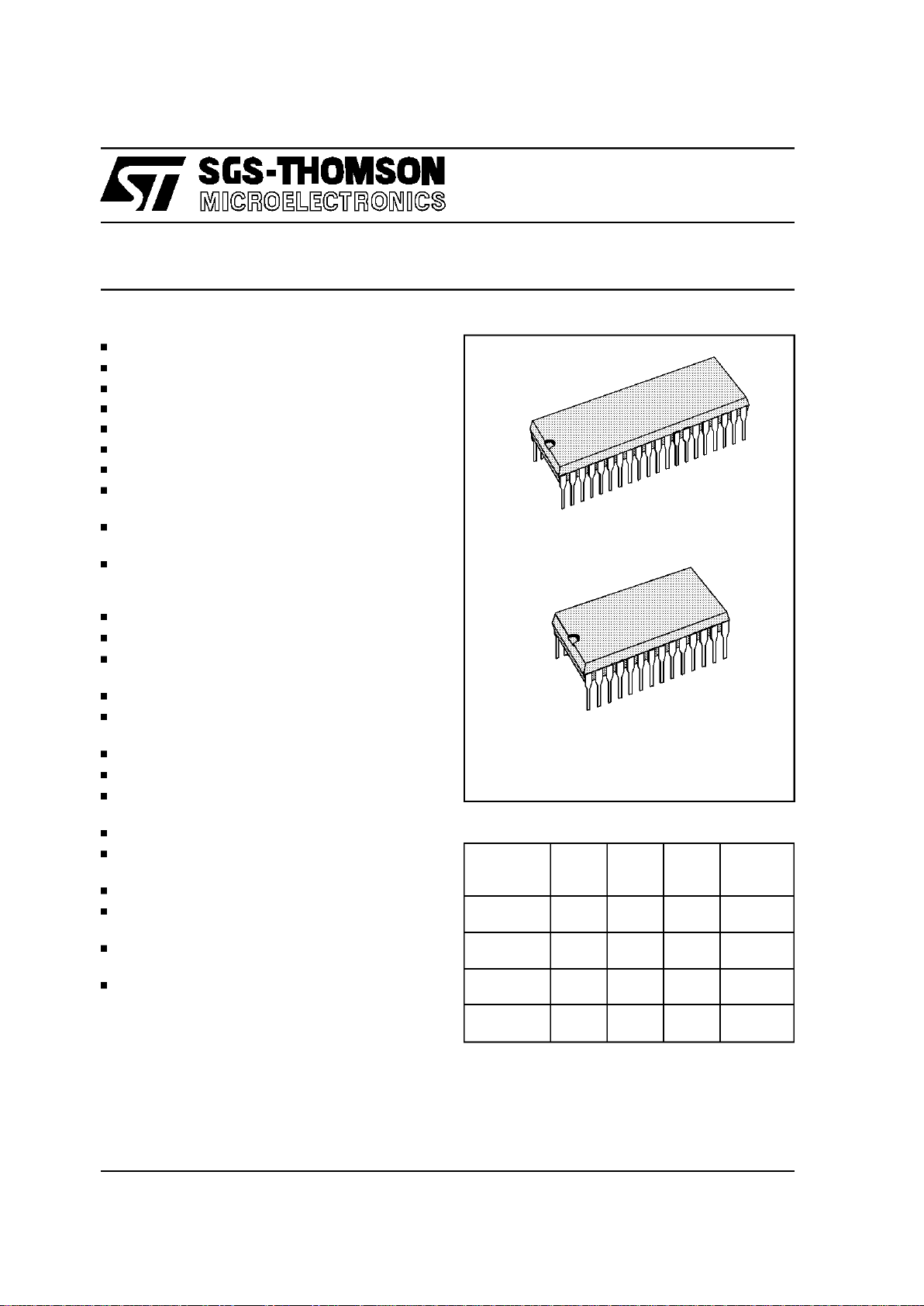
40-Pin Dual in Line Plastic Package for the
ST63126,156
28-Pin Dual in Line Plastic Package for the
ST63140,142
Up to 18 software programmable general pur-
pose Inputs/Outputs, including 8 direct LED
driving Outputs
3 Inputsfor keyboard scan (KBY0-2)
Up to 4 high voltage outputs(BSW0-3)
Two Timerseach includingan 8-bit counter with
a 7-bitprogrammable prescaler
Digital WatchdogFunction
Serial Peripheral Interface(SPI)supporting
S-BUS/I
2
C BUSand standardserial protocols
Up to Four 6-bit PWMD/A Converters
62.5kHz Output pin
14 bitcounter for voltagesynthesis tuning
(ST63156, ST63140)
AFCA/D converterwith 0.5V resolution
Four interrupt vectors (IRIN/NMI, Timer 1 & 2,
VSYNC.)
On-chipclock oscillator
5 Lines by 15 Characters On-ScreenDisplay
Generatorwith 128 Characters(2 banks)
All ROM types are supported by pin-to-pin
EPROMand OTP versions.
The development tool of the ST631xxmicrocon-
trollersconsistsof the ST63TVS-EMUemulation
and development system to be connectedvia a
standard RS232 serial line to an MS-DOSPersonal Computer.
This is Preliminary information from SGS-THOMSON. Details are subject tochange withoutnotice.
October 1993
PRELIMINARY DATA
DEVICE
ROM
(Bytes)
TUN. I/O Pins Package
ST63126 8K FS 12 PDIP40
ST63156 8K VS 11 PDIP40
ST63140 8K VS 6 PDIP28
ST63142 8K FS 6 PDIP28
DEVICE SUMMARY
1
PDIP28
1
PDIP40
(Ordering Information at the end of the datasheet)
1/82
Page 6
Figure1. ST63126, 156 Pin Configuration
Figure2. ST63140, 142 Pin Configuration
DA0
DA3
PC5 (R)
IRIN
OUT1
DA1
DA2
PA1
(SCL) PB5
(SDA) PB6
12
11
10
9
(SEN) PB7
KBY2
KBY
KBY0
8
7
6
5
BSW3
BSW2
BSW0
4
3
2
1
PA3
PA2
21
22
PA4
RESET
OSCin
OSCout
PC1
23
24
25
26
27
28
PA5
PA6
TEST
AFC
(VSYNC) PB2
(HSYNC) PB3
OSDOSCin
OSDOSCout
29
30
31
32
33
34
35
PC6 (G)
PC7 (B)
36
37
38
39
40
VA00282
V
DD
13
14
15
16
17
18
19
20
V
SS
1
BSW1
PC3 (BLANK)
PC2 (ON/OFF)
(1)
PC0
DA0
DA3
PC5 (R)
IRIN
OUT1
DA1
DA2
PA1
(SCL) PB5
(SDA) PB6
12
11
10
9
(SEN) PB7
KBY2
KBY
KBY0
8
7
6
5
BSW3
BSW2
BSW0
4
3
2
1
PA3
PA2
21
22
PA4
RESET
OSCin
OSCout
PC1
23
24
25
26
27
28
PA5
PA6
TEST
AFC
(VSYNC) PB2
(HSYNC) PB3
OSDOSCin
OSDOSCout
29
30
31
32
33
34
35
PC6 (G)
PC7 (B)
36
37
38
39
40
VA00288
V
DD
13
14
15
16
17
18
19
20
V
SS
1
BSW
PC3 (BLANK)
PC2 (ON/OFF)
VS
(1)
BSW0
BSW1
BSW2
KBY0
KBY1
KBY2
OSDOSCout
OSDOSCin
PB3 (HSYNC)
PB2 (VSYNC)
AFC
TEST
PA4
V
DA0
OUT1
VS
PC6 (G)
PC4
PC3 (BLANK)
PC2
OSCout
OSCin
RESET
PA0
PA1
PA2
1
2
3
4
5
6
7
8
9
10
11
12
13
14 15
16
17
18
19
20
21
22
23
24
25
26
27
28
VR001389
DD
V
SS
(1)
BSW0
BSW1
BSW2
KBY0
KBY1
KBY2
OSDOSCout
OSDOSCin
PB3 (HSYNC)
PB2 (VSYNC)
AFC
TEST
PA4
V
V
DA0
OUT1
IRIN
PC6 (G)
PC5 (R)
PC4
PC2
OSCout
OSCin
RESET
PA0
PA1
PA2
1
2
3
4
5
6
7
8
9
10
11
12
13
14 15
16
17
18
19
20
21
22
23
24
25
26
27
28
VR001390
DD
SS
(1)
Note 1. This pin isalso theVPPinputfor EPROM based devices
ST63126
ST63156
ST63140
ST63142
Note 1. This pin isalso theVPPinputfor EPROM based devices
ST63140,142,126,156
2/82
Page 7

GENERAL DESCRIPTION
The ST63140, 142, 126, 156 microcontrollers are
members of the 8-bit HCMOS ST631xx family, a
series of devices specially oriented to TV applications.DifferentROMsizeand peripheralconfigurations areavailableto give themaximumapplication
and cost flexibility. All ST631xx members are
based on a building block approach: a common
core issurrounded by acombinationof on-chipperipherals(macrocells)available from a standard library. These peripherals are designed with the
same Core technology providing full compatibility
and short design time. Many of these macrocells
are specially dedicated to TV applications. The
macrocells of the ST631xx family are: two Timer
peripherals each includingan 8-bit counter with a
7-bit software programmable prescaler (Timer), a
digital hardware activated watchdog function
(DHWD), a 14-bitvoltage synthesis tuningperipheral, a Serial Peripheral Interface (SPI), up to four
6-bit PWM D/A converters,an AFCA/D converter
with 0.5V resolution, an on-screen display (OSD)
with 15 characters per line and 128 characters (in
two bankseach of 64 characters).In addition the
following memory resources are available: program ROM (7K),data RAM(256 bytes),EEPROM
(128 bytes).
Refer to pin configuration figures and to ST631xx
device summary (Table 1) for the definition of
ST631xx family members and asummaryof differences among the different types.
ST63140,142,126,156
3/82
Page 8
STACK LEVEL 1
STACK LEVEL 2
STACK LEVEL 3
STACK LEVEL 4
STACK LEVEL 5
STACK LEVEL 6
PC
D/AOutputs
TIMER 2
IR INTERRUPT
Input
TEST
TIMER 1
PORT C
PORT B
PORT A
VS output &
AFC Input
ON-SCREEN
DISPLAY
DIGITAL
WATCHDOG/TIMER
SERIAL PERIPHERAL
INTERFACE
V
DD
V
SS
OSCin
OSDOSCin OSDOSCout
OSCout
RESET
R, G, B, BLANK
HSYNC (PB3)
VSYNC (PB2)
VR01753E
PA0 - PA7
*
DA0 - DA3
IRIN/NMI
TEST
AFC & VS
*
PB2 - PB7
*
PC0 - PC7
*
POWER SUPPLY OSCILLATOR RESET
8-BIT CORE
USER PROGRAM
ROM
8 KBytes
DATA ROM
USER SELECTABLE
DATA EEPROM
128 Bytes
DATA RAM
256 Bytes
* Refer To Pin Configuration For Additional Information
Figure3. ST631xx Block Diagram
DEVICE
ROM
(Bytes)
RAM
(Bytes)
EEPROM
(Bytes)
I/O
KBY
I/O
BSW
OUT
AFC VS D/A PACK.
EMUL.
DEVICES
ST63126 8K 256 128 12 3 4 YES NO 4 PDIP40 ST63E126
ST63156 8K 256 128 11 3 4 YES YES 4 PDIP40 ST63E156
ST63140 8K 256 128 6 3 3 YES YES 1 PDIP28 ST6E140
ST63142 8K 256 128 6 3 3 YES NO 1 PDIP28 ST63E142
Table 1. Device Summary
ST63140,142,126,156
4/82
Page 9

PIN DESCRIPTION
V
DD
andVSS. Power issupplied to the MCU using
these twopins. V
DD
ispower and VSSistheground
connection.
OSCin, OSCout. These pins are internally con-
nected to the on-chip oscillator circuit. A quartz
crystal or a ceramic resonator can be connected
between these two pins in order to allow the correct operation of the MCU with various stability/cost trade-offs. The OSCin pin is the input pin,
the OSCoutpin is the output pin.
RESET. The activelow RESET pin is used to start
the microcontrollertothe beginningof its program.
TEST. The TEST pin mustbe held at V
SS
for nor-
mal operation.
PA0-PA7. These 8 linesare organizedas oneI/O
port (A). Eachline may be configuredas either an
input or as an output under softwarecontrol of the
data direction register. Port A has an open-drain
(12V drive) output configuration with direct LED
driving capability (30mA,1V).
PB2-PB3,PB5-PB7.These lines are organizedas
one I/O port (B). Each line may be configured as
either aninput withorwithoutinternalpull-up resistor or as an output under software control of the
data direction register. PB2-PB3 have a push-pull
configuration in output mode while PB5-PB7 are
open-drain (5Vdrive).
PB2 and PB3 lines are connected to the VSYNC
and HSYNCcontrol signals ofthe OSD cell;to provide the right signals to the OSD these I/O lines
should beprogrammedin input mode andthe user
can read “on the fly” the state of VSYNC and
HSYNC signals. PB2 is also connected with the
VSYNCInterrupt.The activepolarityofVSYNC Interrupt signalis softwarecontrolled. The activepolarity of these synchronization input pins to the
OSD macrocell can be selected by the user as
ROMmaskoption. Ifthe deviceis specified tohave
negative logic inputs, then when thesesignals are
low the OSD oscillatorstops. If the device is specified to have positivelogic inputs,then when these
signals are highthe OSDoscillatorstops.
PB5, PB6 and PB7 lines, when in output modes,
are “ANDed” with the SPI control signals. PB5 is
connected with the SPI clock signal (SCL), PB6
with the SPI data signal (SDA) while PB7 is connected with SPI enable signal (SEN).
PC0-PC7. These 8 lines are organized as oneI/O
port (C). Each line may be configured as either an
input with or without internal pull-up resistoror as
an output under softwarecontrol of the data direction register.PC0-PC2, PC4have apush-pull configuration in output mode while PC3, PC5-PC7
(OSDsignals)are open-drain(5V drive).PC3,PC5 ,
PC6 and PC7 lines when in output mode are
“ANDed” with the character and blank signals of
the OSD cell. PC3 is connected with the OSD
BLANKsignal,PC5,PC6 and PC7 withthe OSDR,
G and B signals. The active polarity of these signals canbe selected bythe userasROM maskoption. PC2 is also used as TV set ON-OFF switch
(5V drive).
DA0-DA3. These pins are the four PWM D/A outputs (with32kHzrepetition)ofthe6-bit on-chipD/A
converters.The PWM function can be disabledby
software and these lines can be used as general
purpose open-drain outputs (12V drive).
IRIN. This pin is the externalNMI of the MCU.
OUT1. This pin is the 62.5kHz output specially
suited to drivemulti-standard chroma processors.
This functioncan be disabled by software and the
pin can be used as general purpose open-drain
output (12V drive).
BSW0-BSW3. These output pins can be used to
selectupto 4tuningbands.These lines are configured asopen-drainoutputs (12Vdrive).
KBY0-KBY2.Thesepinsareinputonlyand can be
used forkeyboardscan. They have CMOS threshold levels with Schmitt Trigger and on-chip 100kΩ
pull-up resistors.
AFC. This is the input of theon-chip 10 level comparator that can be used to implement the AFC
function. This pin is an high impedance input able
to withstand signals with a peak amplitude up to
12V.
OSDOSCin, OSDOSCout. These are the On
Screen Display oscillator terminals. An oscillation
capacitorand coil network have tobeconnected to
provide theright signal to theOSD.
VS. This is the output pinof theon-chip 14-bitvoltage synthesis tuning cell (VS). The tuning signal
present at this pin gives anapproximate resolution
of 40kHz per stepover the UHFband.This lineis a
push-pull output with standard drive (ST63140,
ST63156 only).
ST63140,142,126,156
5/82
Page 10

Pin Function Description
DA0 to DA3 Output, Open-Drain, 12V
BSW0 to BSW3 Output, Open-Drain, 12V
IRIN Input, Resistive Bias, Schmitt Trigger
AFC Input, High Impedance, 12V
OUT1 Output, Open-Drain, 12V
KBY0 to KBY2 Input, Pull-up, Schmitt Trigger
R,G,B, BLANK Output, Open-Drain, 5V
HSYNC, VSYNC Input, Pull-up, Schmitt Trigger
OSDOSCin Input, High Impedance
OSDOSCout Output, Push-Pull
TEST Input, Pull-Down
OSCin Input, Resistive Bias, Schmitt Trigger to Reset Logic Only
OSCout Output, Push-Pull
RESET Input, Pull-up, Schmitt Trigger Input
VS Output,Push-Pull
PA0-PA6 I/O, Open-Drain, 12V,No Input Pull-up, Schmitt Trigger, High Drive
PB2-PB3, PB5-PB7 I/O, Push-Pull, 5V, Input Pull-up, Schmitt Trigger
PB5-PB7 I/O, Open-Drain, 5V, Input Pull-up, Schmitt Trigger
PC0-PC2, PC4 I/O, Push-Pull, 5V, Input Pull-up, Schmitt Trigger
PC3, PC5-PC7 I/O, Open-Drain, 5V, Input Pull-up, Schmitt Trigger
V
DD,VSS
Power Supply Pins
Table 2. Pin Summary
ST63140,142,126,156
6/82
Page 11
The Core of the ST631xx Family is implemented
independently from the I/O or memory configuration. Consequently,it can be treated as an independent centralprocessorcommunicatingwith I/O
and memoryvia internaladdresses,data,and control busses. The in-core communication is arranged as shown in the following block diagram
figure; thecontrollerbeing externallylinkedto both
the resetand theoscillator, whilethe core is linked
to thededicatedon-chip macrocellsperipheralsvia
the serial data bus and indirectly for interrupt purposes throughthe control registers.
Registers
The ST631xx Family Core has six registers and
three pairs of flags available to the programmer.
They are shown in Figure 5 and are explained in
the following paragraphs together with the program and data memorypage registers.
Accumulator (A). The accumulator is an 8-bit
general purpose register used in all arithmeticcalculations, logical operations, and data manipulations. The accumulator is addressed in the data
space asRAM locationat address FFh.
Accordingly, the ST631xx instruction set can use
the accumulatoras anyother register of the data
space.
VR001811
PROGRAM
ROM/EPROM
RESET
OPCODE
FLAG
VALUES
CONTROL
SIGNALS
12
FLAGS
ALU
A-DATA
B-DATA
2
256
DATA SPACE
DATA
RAM / EEPROM
DATA
ACCUMULATOR
INTERRUPTS
RESULTS TO DATA SPACE ( WRITE LINE )
0,01 TO 8MHz
ADDRESS / READ LINE
DEDICATIONS
CONTROLLER
ROM / EPROM
OSCin OSCout
ADDRESS
DECODER
Program Counter
and
6 LAYER STACK
Figure4. ST631xx Core Block Diagram
SHORT
DIRECT
ADDRESSING
MODE
V REGISTER
W REGISTER
PROGRAMCOUNTER
SIX LEVELS
STACKREGISTER
C
C
C
Z
Z
Z
NORMAL FLAGS
INTERRUPTFLAGS
NMI FLAGS
INDEX
REGISTER
VA000423
b7
b7
b7
b7
b7
b0
b0
b0
b0
b0
b0b11
ACCUMULATOR
Y REG. POINTER
X REG. POINTER
Figure5. ST631xx Core Programming Model
ST631xx CORE
ST63140,142,126,156
7/82
Page 12

ST631xx CORE(Continued)
Indirect Registers (X, Y). These two indirect reg-
istersare usedas pointers tothe memorylocations
in the dataspace. They are usedin theregister-indirect addressing mode.These registers can be
addressed in the data space as RAM locations at
the 80h (X)and 81h (Y)addresses.They can also
be accessed with the direct, short direct, or bit direct addressing modes. Accordingly,the ST631xx
instructionsetcan use the indirect registers as any
other registerof the data space.
Short Direct Registers (V, W). These two registers are used to save one byte in short direct addressing mode.These registerscan be addressed
in the data space as RAM locations atthe 82h (V)
and 83H (W) addresses. They can also be accessed with the direct and bit direct addressing
modes. Accordingly, the ST631xx instruction set
can use the shortdirect registers as any other register ofthe data space.
Program Counter (PC)
The program counter is a 12-bit registerthat contains the address of the next ROM location to be
processed by the core. This ROM location may be
an opcode, an operand, or an address of operand.
The 12-bit length allows the direct addressing of
4096 bytes in the program space. Nevertheless, if
the program space contains more than 4096 locations, thefurtherprogram spacecan be addressed
by using theProgramROMPage Register.The PC
value isincremented,after it is read forthe address
of thecurrent instruction,by sendingit through the
ALU, so giving the addressof the next byte in the
program.Toexecuterelativejumpsthe PCand the
offset values are shifted through the ALU, where
they will be added, and the result is shifted back
into the PC. The program countercan be changed
in thefollowingways:
JP (Jump)instruction....PC= Jump address
CALL instruction...........PC=Call address
Relative Branch
instructions...................PC= PC+offset
Interrupt........................PC=Interrupt vector
Reset............................PC=Reset vector
RET &RETI instructions............PC=Pop (stack)
Normal instruction........PC= PC+1
Flags (C, Z)
The ST631xx Core includes three pairs of flags
that correspond to 3 different modes: normal
mode, interrupt mode and Non-Maskable-Interrupt-Mode. Each pair consists of a CARRY flag
and aZEROflag. One pair (CN,ZN) is used during
normal operation, one pair is used during the interrupt mode (CI,ZI) and one is used during the notmaskable interrupt mode (CNMI,ZNMI).
TheST631xxCoreuses the pairofflags that corresponds to the actualmode: as soonas aninterrupt
(resp.a Non-Maskable-Interrupt)isgenerated, the
ST631xx Core uses the interrupt flags (resp. the
NMI flags) instead of the normal flags. When the
RETI instruction is executed, the normal flags
(resp. the interrupt flags) are restoredif the MCU
was in the normal mode (resp. in the interrupt
mode) before the interrupt. Should be observed
that each flagset can only be addressedin its own
routine (Not-maskable interrupt, normal interrupt
or mainroutine).Theinterrupt flags arenot cleared
during thecontext switching and so, theyremain in
the state they were at the exit of the last routine
switching.
The Carry flag is set when a carry or a borrow occurs during arithmetic operations, otherwise it is
cleared. The Carry flag is also set to the value of
the bit tested in a bit test instruction, and participates in the rotate left instruction.
TheZeroflagissetif theresultofthelastarithmetic
or logical operation wasequal to zero, otherwise it
is cleared.
The switching between these three sets is automaticallyperformedwhen anNMI,an interrupt and
a RETI instructions occur. As the NMI mode is
automatically selected after the reset ofthe MCU,
the ST631xxCore uses at firstthe NMI flags.
ST63140,142,126,156
8/82
Page 13

ST631xxx CORE(Continued)
Stack
The ST631xx Core includes true LIFO hardware
stack that eliminates the need fora stack pointer.
The stackconsists ofsixseparate12-bit RAMlocations that do not belong to the data space RAM
area. When a subroutine call (or interruptrequest)
occurs,the contentsofeach levelis shiftedinto the
next levelwhile the contentofthe PC is shiftedinto
the first level (the value of the sixth level will be
lost). When subroutine or interrupt return occurs
(RET or RETI instructions), the first levelregisteris
shifted back into the PCand thevalue ofeachlevel
is shifted back into the previous level. These two
operating modes are describedin Figure 6. Since
the accumulator,as all otherdata space registers,
is not stored inthis stack the handling ofthisregisters shall be performed inside the subroutine. The
stack pointer will remain in its deepest position,if
more than 6 calls or interrupts are executed, so
that the last return address will be lost. It will also
remain in its highest position if the stack is empty
and a RET or RETI is executed. In this case the
next instructionwill be executed.
WHEN CALL
OR
INTERRUPT REQUEST
OCCURS
STACK LEVEL 1
STACK LEVEL 1
STACK LEVEL 1
STACK LEVEL 1
STACK LEVEL 1
STACK LEVEL 1
PROGRAM COUNTER
RET OR RETI
WHEN
OCCURS
VA000424
Figure6. Stack Operation
ST63140,142,126,156
9/82
Page 14
PROGRAM SPACE
VR001568
INTERRUPT &
RESET VECTORS
ACCUMULATOR
WREGISTER
RAM
DATA ROM
WINDOW
RAM / EEPROM
BANKING AREA
DATA SPACE
DATA RAM
BANK SELECT
DATA ROM
WINDOW SELECT
VREGISTER
YREGISTER
XREGISTER
0-63
0000h
07FFh
0800h
0FF0h
0FFFh
000h
03Fh
040h
070h
080h
081h
082h
083h
084h
0FFh
0C0h
ROM
ROM
STACKLEVEL 1
STACKLEVEL 2
STACKLEVEL 3
STACKLEVEL 4
STACKLEVEL 5
STACKLEVEL 6
PROGRAM COUNTER
STACK SPACE
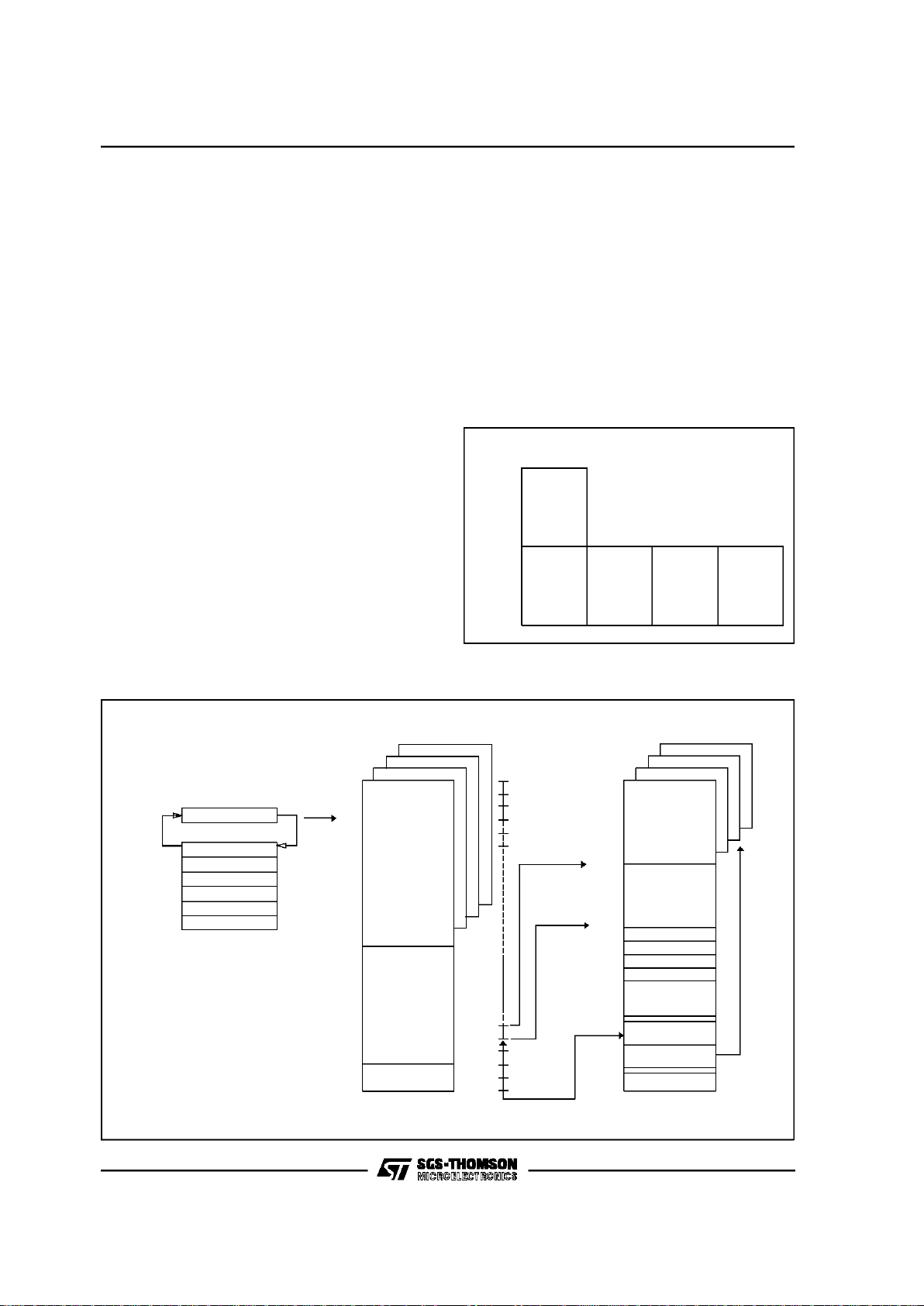
Figure7. ST631xx Memory AddressingDescription Diagram
MEMORY SPACES
The MCUs operate in three different memory
spaces: Program Space, Data Space, and Stack
Space. A descriptionof these spaces is shown in
the followingFigures.
Program Space
The program space is physically implemented in
the ROM and includes all the instructionsthat are
to be executed, as well as the data requiredforthe
immediate addressing mode instructions, the reserved test area and uservectors. It is addressed
thanks to the 12-bit Program Counter register (PC
register)andso, the ST631xxCore can directlyaddress upto 4K bytesof Program Space.Nevertheless, the ProgramSpace can be extended by the
addition of 2-KbyteROM banks as it is shown in
Figure 8 in which the 8K bytes memory is described.
These banks are addressed by pointing to the
000h-7FFhlocations of the Program Spacethanks
to the Program Counter, and by writing the appropriate code in the Program ROM Page Register
(PRPR) located at address CAh of the Data
Space. Because interrupts and common subroutines should beavailableall the time onlythe lower
2K bytes of the 4K program space are bank
switched while the upper 2K bytescan be seen as
Program
counter
space
0000h 1FFFh
0FFFh
Static Page
Page 1
0800h
07FFh
Page 0
Page 1
Static Page
Page 2 Page 3
0000h
Figure8. ST631xx 8K Bytes ProgramSpace
AddressingDescription
staticspace. Table 3givesthecodesthat allow the
selection of the correspondingbanks.
Note that,fromthe memory point of view,thePage
1 and the StaticPage represent the same physical
memory:it isonly adifferentway ofaddressingthe
same location. On the ST631xx a total of 8192
bytes of ROM have been implemented; 7948 are
availableas user ROM while 244 are reserved for
testing.
ST63140,142,126,156
10/82
Page 15
D7-D2. These bits are not used.
PRPR1-PRPR0. These are the program ROM
banking bits and thevalue loaded selects the corresponding page to be addressedin the lower part
of 4K programaddressspaceasspecifiedinTable3.
This registeris undefinedon reset.
Note:
Only the lower part of address space has been
bankswitched because interrupt vectors and common subroutines should be availableall the time.
The reasonof this structureis due tothe fact thatit
is notpossible tojump froma dynamic page to another, unless jumping back to the static page,
changingcontents of PRPR,and, then,jumping to
a differentdynamic page.
PRPR1 PRPR0 PC11 Memory Page
X X 1 Static Page (Page1)
0 0 0 Page 0
0 1 0 Page 1 (Static Page)
1 0 0 Page 2
1 1 0 Page 3
Table 3. Program ROM Page Register Coding
Care is required when handlingthe PRPR as it is
write only. For this reason, it is not allowed to
change the PRPR contents while executing interrupts drivers, as the driver cannot save and than
restore its previous content. Anyway, this operation may be necessary if thesum ofcommon routines and interrupt driverswill take more than 2K
bytes; in this case could benecessaryto divide the
interrupt driver in a (minor) part in the static page
(start and end), and in the second (major) part in
one dynamic page. If it is impossible to avoid the
writing of this register in interrupts drivers, an image of this register must be saved in a RAMlocation, and eachtime theprogramwrites the PRPRit
writes also the image register.The image register
must be written first, so if an interruptoccurs between the two instructions the PRPR is not affected.
MEMORY SPACES(Continued)
PRPR
Program ROMPage Register
(CAh, Write Only)
D7 D6 D5 D4 D3 D2 D1 D0
PRPR0 = PROG.ROMSelect0
PRPR1 = PROG.ROMSelect1
UNUSED
UNUSED
UNUSED
UNUSED
UNUSED
UNUSED
Figure11. Program ROM Page Register
ROM Page Device Address Device Address
(1)
Description
PAGE 0
0000h-007Fh
0080h-07FFh
0000h-007Fh
0080h-07FFh
Reserved
User ROM
PAGE 1
“STATIC”
0800h-0F9Fh
0FA0h-0FEFh
0FF0h-0FF7h
0FF8h-0FFBh
0FFCh-0FFDh
0FFEh-0FFFh
0800h-0F9Fh
0FA0h-0FEFh
0FF0h-0FF7h
0FF8h-0FFBh
0FFCh-0FFDh
0FFEh-0FFFh
User ROM
Reserved
Interrupt Vectors
Reserved
NMI Vector
Reset Vector
PAGE 2
0000h-000Fh
0010h-07FFh
1000h-100Fh
1010h-17FFh
Reserved
User ROM
PAGE 3
0000h-000Fh
0010h-07FFh
1800h-180Fh
1810h-1FFFh
Reserved
User ROM
Table 4. ST631xx Program ROM Map
Note 1. EPROM addresses relate to the use of ST63E1xx EPROMEmulation device.
This register is undefined on reset. Neither
read nor single bit instructions may be used to
address thisregister.
ST63140,142,126,156
11/82
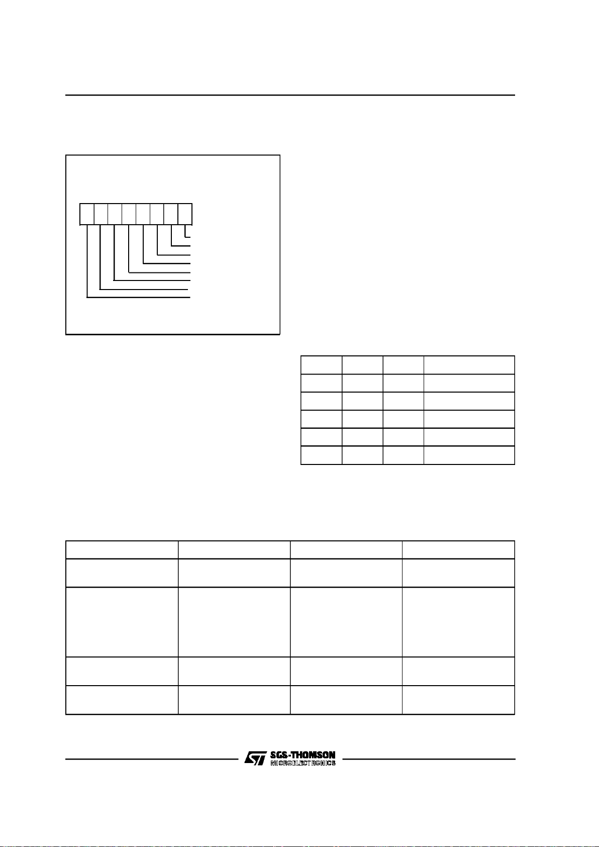
Page 16
b7 b0
000h
DATA RAM/EEPROM/OSD
BANK AREA
03Fh
040h
DATA ROM
WINDOW AREA
07Fh
X REGISTER 080h
Y REGISTER 081h
V REGISTER 082h
W REGISTER 083h
084h
DATA RAM
0BFh
PORT A DATA REGISTER 0C0h
PORT B DATA REGISTER 0C1h
PORT C DATA REGISTER 0C2h
RESERVED 0C3h
PORT ADIRECTION REGISTER 0C4h
PORT BDIRECTION REGISTER 0C5h
PORT C DIRECTION REGISTER 0C6h
RESERVED 0C7h
INTERRUPT OPTION REGISTER 0C8h
DATA ROMWINDOW REGISTER 0C9h
PROGRAM ROM PAGEREGISTER 0CAh
RESERVED 0CBh
SPIDATA REGISTER 0CCh
0CDh
RESERVED
0D1h
TIMER 1 PRESCALER REGISTER 0D2h
TIMER 1COUNTER REGISTER 0D3h
TIMER 1 STATUS/CONTROL REG. 0D4h
0D5h
RESERVED
0D7h
WATCHDOG REGISTER 0D8h
Figure12. ST631xx Data Space
b7 b0
RESERVED 0D9h
TIMER 2 PRESCALER REGISTER 0DAh
TIMER 2 COUNTER REGISTER 0DBh
TIMER 2 STATUS CONTROL REG. 0DCh
0DDh
RESERVED
0DFh
DA0 DATA/CONTROL REGISTER 0E0h
DA1 DATA/CONTROL REGISTER 0E1h
DA2 DATA/CONTROL REGISTER 0E2h
DA3 DATA/CONTROL REGISTER 0E3h
AFC RESULTREGISTER 0E4h
KEYBOARDINPUT REGISTER 0E5h
RESERVED 0E6h
RESERVED 0E7h
DATA RAM BANK REGISTER 0E8h
BSWCONTROL REGISTER 0E9h
EEPROM CONTROL REGISTER 0EAh
SPI CONTROL REGISTER 1 0EBh
SPI CONTROL REGISTER 2 0ECh
VS DATA REGISTER 1 0EDh
VS DATA REGISTER 2 0EEh
OSD CHARAC. BANK SELECTREG. 0EFh
0F0h
RESERVED
0FEh
ACCUMULATOR 0FFh
OSDCONTROLREGISTERSLOCATED
IN PAGE6 OFBANKED DATA RAM
VERTICAL STARTADDRESS REG. 010h
HORIZONTALSTARTADDRESSREG. 011h
VERTICAL SPACEREGISTER 012h
HORIZONTAL SPACEREGISTER 013h
BACKGROUND COLOUR REGISTER 014h
GLOBAL ENABLEREGISTER 017h
Figure13. ST631xx Data Space(Continued)
MEMORY SPACES(Continued)
Data Space
The instruction set of the ST631xx Core operates
on a specificspace, named DataSpace that contains all the data necessary for the processingof
the program. The Data Space allows the address-
ing of RAM (256 bytes for the ST631xx family),
EEPROM (128 bytes), ST631xx Core/peripheral
registers, and read-only data such as constants
and thelook-up tables.
ST63140,142,126,156
12/82
Page 17

DWR
Data ROMWindow Register
(C9h, Write Only)
D7 D6 D5 D4 D3 D2 D1 D0
DWR0 = Data ROMWindow 0
DWR1 = Data ROMWindow 1
DWR2 = Data ROMWindow 2
DWR3 = Data ROMWindow 3
DWR4 = Data ROMWindow 4
DWR5 = Data ROMWindow 5
DWR6 = Data ROMWindow 6
UNUSED
Figure14. Data ROM Window Register
Data ROMAddressing.All theread-only data are
physically implemented in the ROM in which the
Program Space is also implemented. The ROM
thereforecontains theprogram tobe executedand
also the constants and the look-up tables needed
for the program. The locations of Data Space in
which the different constants and look-up tables
are addressed by the ST631xx Core can be considered as being a 64-byte window throughwhich
it ispossible toaccessto the read-only data stored
in the ROM. This window is located from address
40H toaddress 7Fh in the Dataspace and allows
the direct reading of the bytes from the address
000h to address03Fh in the ROM. All the bytesof
the ROMcan be usedto storeeither instructionsor
read-onlydata. Indeed,the window can be moved
by step of 64 bytes along the ROM in writing the
appropriatecodein the Write-only Data ROMWindow register(DRWR, location C9h).The effective
address ofthebyteto beread as adata in theROM
is obtained by the concatenation of the 6 lesssignificant bits of the addressin the Data Space (as
less significant bits)and the contentof theDRWR
(as most significant bits). So when addressing location 40h of data space, and 0 isloaded in the
DRWR, the physicaladdressed location in ROMis
00h.
D7. This bit is not used.
DWR6-DWR0.ThesearetheDataRomW in dowbits
thatcorrespondtotheupperbitsofdataROMprogram
space.Thisregisterisundefinedafterreset.
This register is undefined on reset. Neither
read nor single bit instructions may be usedto
address thisregister.
Note. Care is required when handlingthe DRWR
as it is write only. For this reason, it is not allowed
to change the DRWRcontents while executinginterruptsdrivers,as the drivercannot saveand than
restore its previous content. If it is impossible to
avoid the writing of this register in interrupts drivers, an image of this register must be saved in a
RAM location, and each time the program writes
the DRWRitwritesalsothe image register.The image register must be writtenfirst,so if an interrupt
occurs between the two instructions the DRWR
register is not affected.
MEMORY SPACES(Continued)
DATA ROM
WINDOW REGISTER
CONTENTS
DATA SPACE ADDRESS
40h-7Fh
IN INSTRUCTION
PROGRAM SPACE ADDRESS
65432 0
543210
543210
READ
1
67891011
0
1
VR01573B
12
1
0
DATA SPACE ADDRESS
59h
0000
0
1
00
1
11
Example:
(DWR)
DWR=28h
11000000001
ROM
ADDRESS:A19h
11
13
01
7
0
0
Figure15. Data ROM Window Memory Addressing
ST63140,142,126,156
13/82
Page 18

DRBR
Data RAM
Bank Register
(E8h, Write Only)
D7 D6 D5 D4 D3 D2 D1 D0
DRBR0 = Data RAM Bank0
DRBR1= Data RAM Bank 0
DRBR2= Data RAM Bank 0
DRBR3= Data RAM Bank 0
DRBR4= Data RAM Bank 0
DRBR5= Data RAM Bank 0
DRBR6= Data RAM Bank 0
UNUSED
Figure16. Data RAM Bank Register
MEMORY SPACES(Continued)
Data RAM/EEPROM/OSDRAM Addressing
In all members of the ST631xx family 64 bytes of
data RAM are directly addressable in the data
space from 80h toBFh addresses.The additional
192 bytesof RAM, the 128 bytesof EEPROM,and
the OSD RAM can be addressedusing the banks
of 64 bytes located between addresses 00h and
3Fh.Theselection of the bankisdone byprogramming theDataRAM BankRegister(DRBR)located
at the E8h address of the Data Space. In thisway
each bankofRAM,EEPROMorOSDRAMcan select 64 bytes at a time. No more than one bank
should beset at a time.
D7. This bit is not used.
DRBR6, DRBR5.Each of these bits, when set,will
selectone OSDRAM register page.
DRBR4,DRBR3,DRBR2.Each of these bits,when
set,will select one RAM page.
DRBR1,DRBR0. These bits select the EEPROM
pages.
This register is undefined after reset. Neither
read nor single bit instructions may be used to
address thisregister.
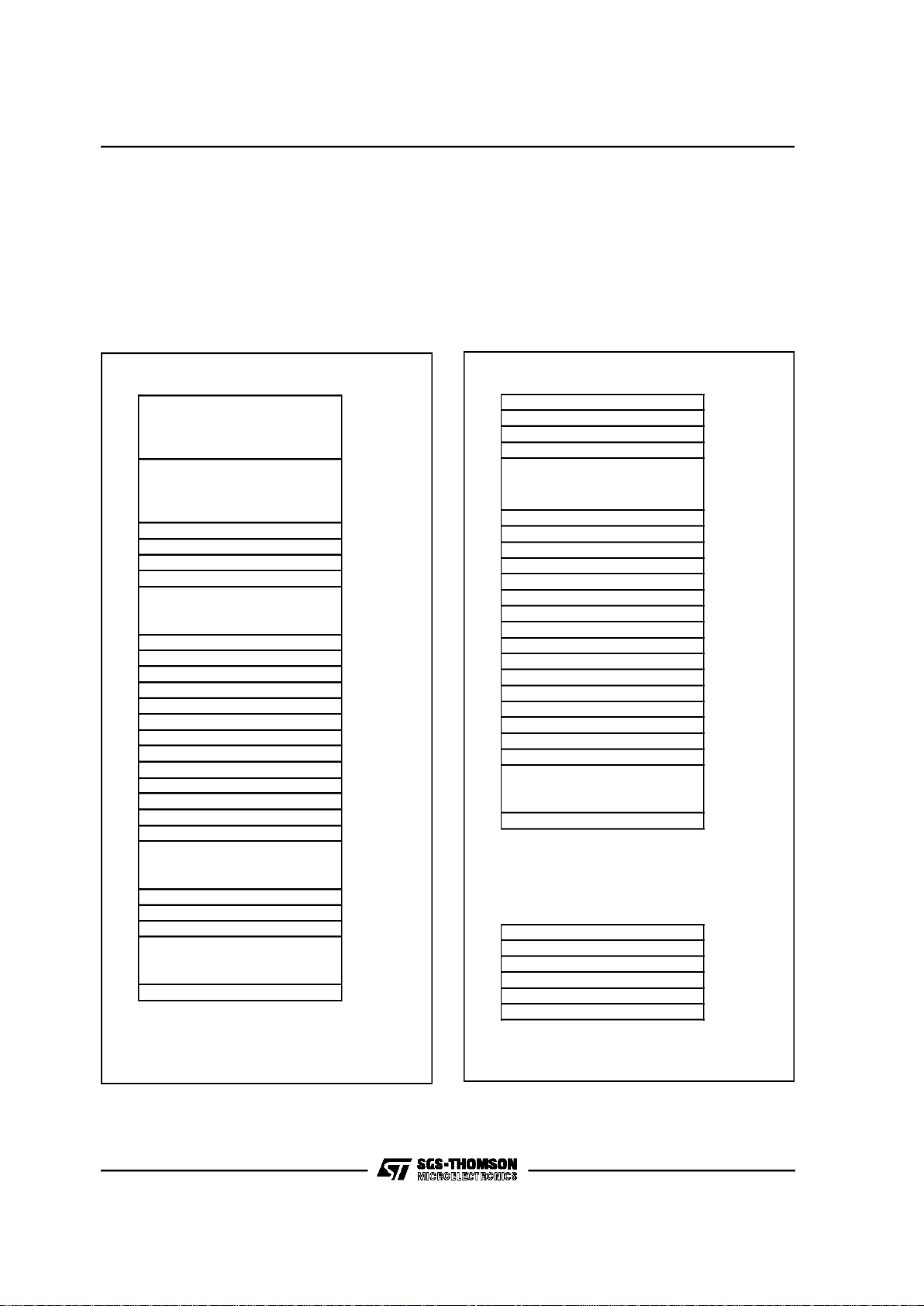
Table 5 summarizes how to set the Data RAM
Bank Register in order to select the various banks
or pages.
Note :
Care is required when handling the DRBR asit is
write only. For this reason, it is not allowed to
change the DRBR contentswhile executing interrupts drivers, as the driver cannot save and than
restore its previous content. If it is impossible to
avoid the writing of this register in interrupts drivers, an image of this register must be saved in a
RAM location, and each time the program writes
the DRBRit writes also the image register.
The image registermustbe written first,so if an interrupt occurs between the two instructions the
DRBR is not affected.
DRBR Value
Selection
Hex. Binary
01h 0000 0001 EEPROM Page 0
02h 0000 0010 EEPROM Page 1
04h 0000 0100 RAM Page 2
08h 000 1000 RAM Page 3
10h 0001 0000 RAM Page 4
20h 0010 0000 OSD Page 5
40h 0100 0000 OSD Page 6
Table 5. Data RAMBank Register Set-up
ST63140,142,126,156
14/82
Page 19

EEPROMDescription
The dataspace of ST631xxfamily from 00hto 3Fh
is paged as described in Table 5. 128 bytes of
EEPROMlocated in 2 pagesof 64 bytes (pages0,
and 1, see Table 5).
Through the programming of the Data RAM Bank
Register (DRBR=E8h) the user can select the
bank or page leaving unaffected the way to address the static registers. The way to address the
“dynamic”page is tosetthe DRBRas described in
Table 5(e.g.to selectEEPROMpage 0,the DRBR
has to be loaded with content 01h, see Data
RAM/EEPROM/OSD RAM addressing for additional information). Bits 0 and 1 of the DRBR are
dedicated tothe EEPROM.
The EEPROM pages do not require dedicated instructionstobeaccessed in reading or writing.The
EEPROM is controlled by the EEPROM Control
Register (EECR=EAh).AnyEEPROMlocation can
be read just like any other data location, also in
terms ofaccesstime.
To write an EEPROM location takes an average
time of 5 ms (10ms max) and during this timethe
EEPROM is not accessible by the Core. A busy
flag canbe readby the Coretoknow the EEPROM
status before trying any access. In writing the
EEPROM can work in two modes: Byte Mode
(BMODE) and Parallel Mode (PMODE). The
BMODE is the normal way to use the EEPROM
and consists in accessing one byte at a time. The
PMODE consists inaccessing 8 bytesper time.
D7. Not used
SB.WRITEONLY. Ifthis bit isset theEEPROMis
disabled (any accesswill be meaningless)and the
power consumption of the EEPROMis reducedto
the leakage values.
D5, D4.Reserved,they must be setto zero.
PS.SET ONLY. Oncein Parallel Mode,assoon as
the usersoftwaresets the PSbitthe parallelwriting
of the 8 adjacentregisters will start.PSis internally
reset at the end of the programming procedure.
Note that less than 8 bytes can be written; after
parallel programming the remaining undefined
bytes will haveno particular content.
PE.WRITE ONLY. This bit must be setby theuser
program in order to performparallel programming
(more bytes per time). IfPE is set and the “parallel
start bit” (PS) is low, up to8 adjacentbytes can be
written at the maximum speed, the content being
stored in volatile registers.These 8 adjacent bytes
can be considered as row, whose A7, A6, A5, A4,
A3 arefixed while A2, A1 and A0 are thechanging
bytes. PE is automatically reset at the end of any
parallelprogramming procedure.PE can be reset
by the user software before starting the programming procedure,leaving unchanged theEEPROM
registers.
BS.READ ONLY. This bit will be automaticallyset
by the CORE when the user program modifies an
EEPROMregister. The user program hasto test it
before any read or write EEPROM operation; any
attemptto access the EEPROM while “busy bit” is
setwillbeabortedandthewriting procedureinprogress completed.
EN. WRITE ONLY.This bit MUSTbe set to one in
order to write any EEPROM register. If the user
program will attempt to write the EEPROM when
EN= “0” the involved registers will be unaffected
and the“busy bit”will notbe set.
AfterRESETthecontentofEECRregist erwi llbe 00h.
Notes :
When the EEPROM is busy (BS=“1”) the EECR
can notbe accessed inwrite mode, it is only possible to read BSstatus.This implies that as long as
the EEPROM is busy it is not possible to change
the status of the EEPROM control register. EECR
bits 4 and 5 are reserved for test purposes, and
must never be set to “1”.
MEMORY SPACES(Continued)
EECR
EEPROM Control Register
(EAh, Read/Write)
D7 D6 D5 D4 D3 D2 D1 D0
EN = EEPROMEnable Bit
BS = EEPROM Busy Bit
PE = Parallel Mode Enable Bit
PS = Parallel Start Bit
Reserved (Mustbe set Low)
Reserved (Mustbe set Low)
SB =Stand-by Enable Bit
Unused
Figure17. EEPROM Control Register
ST63140,142,126,156
15/82
Page 20

Additional Notes on Parallel Mode. If the user
wants to perform a parallel programming the first
action should be the set toone thePEbit; from this
moment the first time the EEPROM will be addressed in writing, the ROW address will be
latched and it will be possible to change it only at
the end ofthe programmingprocedureor by resetting PE without programming the EEPROM.After
the ROWaddress latching the Core can “see” just
one EEPROMrow (the selected one) and any attempt to write or read other rows will produceerrors. Donot read the EEPROMwhile PEis set.
As soon asPE bitis set,the 8volatile ROW latches
are cleared. From this moment the user can load
data in the whole ROW or just in a subset.PS setting willmodify the EEPROMregisterscorresponding to the ROW latches accessed after PE. For
example, if the software sets PE and accesses
EEPROM in writing at addresses 18h,1Ah,1Bh
and then sets PS, these three registers will be
modified atthe same time; theremainingbytes will
have no particular content. Note that PE is internally reset at the end of the programming procedure. This implies that the user must set PE bit
between two parallel programming procedures.
Anywaytheuser can set andthen resetPEwithout
performing any EEPROM programming. PS is a
set only bit and is internally reset atthe end of the
programming procedure. Note that ifthe usertries
to set PS while PE is not set there will not be any
programming procedure and thePS bit will be unaffected.Consequently PS bitcan notbe set if EN
is low. PS can be affectedby the user set if, and
only if,EN and PE bits are also set to one.
STACK SPACE
The stackspace consistsof six 12bit registersthat
are used for stacking subroutine and interrupt return addresses plus the current program counter
register.
MEMORY SPACES(Continued)
INTERRUPT
The ST631xxCore can manage 4 different maskable interrupt sources, plus one non-maskable interrupt source (top priority level interrupt). Each
sourceisassociated with aparticularinterruptvector that contains a Jump instruction to the related
interrupt serviceroutine. Each vector is located in
the Program Space at a particular address (see
Table 6). When a source provides an interruptrequest, and therequest processingis alsoenabled
by the ST631xx Core, then the PC register is
loaded withthe address of the interrupt vector (i.e.
of the Jump instruction). Finally, the PC is loaded
with theaddress of the Jumpinstructionand the interruptroutine isprocessed.
The relationship between vector and source and
the associatedpriority ishardware fixed for the different ST631xx devices. For some interrupt
sourcesit is also possible to selectby softwarethe
kind ofevent that will generate the interrupt.
All interruptscan be disabled by writingto theGEN
bit (global interruptenable) of the interrupt option
register(addressC8h). Aftera reset,ST631xxis in
non maskable interruptmode, so no interruptswill
be accepted and NMI flags will be used, until a
RETI instruction is executed.If an interruptis executed, one special cycle is made by the core,during that the PC is set to the related interrupt vector
address. A jump instructionat thisaddress has to
redirect program execution to thebeginningof the
relatedinterruptroutine.Theinterruptdetectingcycle, also resets the relatedinterrupt flag(not available to the user), so that another interrupt can be
stored for this current vector, while its driver is under execution.
If additionalinterruptsarrivefromthe same source,
they will be lost. NMI can interrupt other interrupt
routines at any time,while other interrupts cannot
interrupt each other. If more than one interrupt is
waiting forservice, they are executed according to
their priority. The lower the number, the higher the
priority. Priority is, therefore, fixed. Interrupts are
checked during the last cycle of an instruction
(RETIincluded). Level sensitive interrupts have to
be validduring this period.
ST63140,142,126,156
16/82
Page 21
InterruptVectors/Sources
The ST631xx Core includes 5 different interrupt
vectors in order to branch to 5 different interrupt
routines. The interrupt vectors are located in the
fixed (or static)page of the Program Space.
The interruptvectorassociatedwith thenon-maskable interrupt source is named interrupt vector#0.
It is located at addresses FFCh,FFDh in the Program Space. This vector is associated with the
PC6/IRINpin.
The interrupt vectors located at addresses
(FF6h,FF7h), (FF4h,FF5h), (FF2h,FF3h),
(FF0h,FF1h) are named interrupt vectors #1, #2,
#3 and #4respectively.These vectorsare associated with TIMER 2 (#4), VSYNC (#2), and TIMER
1 (#3). Interrupt vector (#1) is not used on
ST631xx.
InterruptPriority
The non-maskable interrupt request has the highest priority and can interrupt any other interrupt
routines at any time, nevertheless the other interrupts cannot interrupteach other. Ifmore than one
interrupt requestis pending,they areprocessedby
the ST631xx Core according to their prioritylevel:
vector#1 has the higherprioritywhile vector#4the
lower. Thepriority of each interrupt sourceis hardware fixed.
InterruptOption Register
The Interrupt Option Register (IOR register, location C8h) is used to enable/disable the individual
interrupt sources and to select the operating mode
of theexternal interrupt inputs.Thisregistercanbe
addressed in the Data Space as RAM location at
the C8h address,nevertheless it is write-only register that can not be accessed with single-bit operations. The operating modes of the external
interrupt inputs associated to interrupt vectors #1
and #2are selectedthrough bits5 and6 of theIOR
register.
Interrupt
Source
Associated
Vector
Vector Address
IRIN/NMI
Pin
(1)
Interrupt
Vector # 0 (NMI)
0FFCh-0FFDh
None
(2)
Interrupt
Vector # 1
0FF6h-0FF7h
Vsync
Interrupt
Vector # 2
0FF4h-0FF5h
Timer 1
Interrupt
Vector # 3
0FF2h-0FF3h
Timer 2
Interrupt
Vector # 4
0FF0h-0FF1h
Notes:
1. This pin is associated with the NMIInterrupt Vector
2. This vectoris not used in ST631xx.
Table 6. Interrup tVectors/SourcesRelati ons hi ps
INTERRUPT(Continued)
IOR
InterruptOption Register
(C8h, Write Only)
D7 D6 D5 D4 D3 D2 D1 D0
Unused
GEN = Global EnableBit
ES2 = Edge SelectionBit
EL1 = EdgeLevelSelection Bit
Unused
Figure18. InterruptOption Register
D7. Not used.
EL1. This is the Edge/Level selection bit of inter-
rupt#1.When set to one,the interruptisgenerated
on low level of the related signal; when cleared to
zero,the interruptisgenerated on falling edge.The
bit iscleared tozero after reset and as nointerrupt
source is associated to vector#1 on ST631xx, the
user must keepthis bit atzeroto avoid ghostinterruptsfrom this source.
ES2. This is the edge selection bit on interrupt#2.
This bit is used on the ST631xx devices with onchip OSDgenerator for VSYNC detection.
GEN.This isthe global enablebit. When setto one
all interrupts are globallyenabled; when thisbit is
cleared to zero all interruptsare disabled(EXcluding NMI).
D3 - D0. Thesebits are not used.
ST63140,142,126,156
17/82
Page 22

Interrupt Procedure. The interrupt procedure is
very similar to a call procedure, indeed the user
can considerthe interrupt asan asynchronouscall
procedure. As this is an asynchronous event the
user doesnot know about the contextand the time
at which it occurred. As a result the user should
saveall the dataspace registerswhich willbe used
inside the interrupt routines. There are separate
sets of processor flags for normal, interrupt and
non-maskable interrupt modes whichare automatically switched and so these do not need to be
saved.
The following list summarizes the interrupt procedure:
ST631xxactions
-
Interrupt detection
-
The flags C and Z of the main routine are exchanged with the flags C and Z of the interrupt
routine (orthe NMI flags)
-
The valueof thePC is storedin the firstlevel of
the stack
-
The normal interrupt lines are inhibited (NMI
still active)
-
First internal latch is cleared
-
The relatedinterrupt vectoris loaded inthe PC.
User actions
-
User selected registers are saved insidethe interrupt service routine (normally on a software
stack)
-
The source of the interrupt is found by polling
(if more than one source is associated to the
same vector)the interrupt flag of the source.
-
Interrupt servicing
-
Return from interrupt (RETI)
ST631xxactions
-
Automatically the ST631xx core switches back
to the normal flags (or the interrupt flags) and
pops the previous PC value fromthe stack
The interruptroutine begins usually by the identification of the device that has generated the interrupt request (bypolling).The user should save the
registers which are used inside the interrupt routine (thatholds relevantdata)intoa softwarestack.
After the RETIinstruction execution, the corecarries out theprevious actions and the main routine
can continue.
ST631xx InterruptDetails
IR Interrupt (#0). The IRIN Interrupt is connected
to the firstinterrupt #0 (NMI,0FFCh). If enabled,
then an interruptwill begenerated ona rising edge
at the pin.
Interrupt(#1).OnST631xx no sourcesareassociated to vector (#1). To avoid any ghost interrupt
due to interrupt(#1) the user must keep the EL1
bit ofIOR registerto zero.
INTERRUPT(Continued)
LOAD PC FROM
INTERRUPT VECTOR
( FF C / FFD )
SET
INTERRUPT MASK
PUSH THE
PC INTO THE STACK
SELECT
INTERNAL MODE FLAG
CHECK IF THERE IS
AN INTERRUPT REQUEST
AND INTERRUPT MASK
INSTRUCTION
WAS
THE INSTRUCTION
ARETI
IS THE CORE
ALREADY IN
NORMAL MODE ?
FETCH
INSTRUCTION
EXECUTE
INSTRUCTION
CLEAR
INTERRUPT MASK
SELECT
PROGRAM FLAGS
” POP ”
THE STACKED PC
NO
NO
YES
YES
?
?
NO
YES
VA000014
Figure19. InterruptProcessingFlow-Chart
ST63140,142,126,156
18/82
Page 23

INTERRUPT(Continued)
VSYNC Interrupt (#2). The VSYNC Interrupt is
connected to the interrupt #2. When disabled the
VSYNC INT signal is low.Bit 5of the interrupt option register C8h is used to select the negative
edge (ES2=0) or the positive edge (ES2=1); the
edge willdependontheapplication.Notethat once
an edge has been latched, then the only wayto remove the latched signal is to service the interrupt.
Care mustbe takennotto generatespurious interrupts. This interruptmay be used for synchronize
to theVSYNCsignal inorder tochange characters
in the OSD only when the screen is on vertical
blanking (if desired). This method may also be
used toblink characters.
TIMER 1 Interrupt(#3). The TIMER 1 Interruptis
connected to the fourth interrupt#3 (0FF2h) which
detectsa low level(latched in the timer).
TIMER 2 Interrupt(#4). The TIMER 2 Interruptis
connected to the fifth interrupt #4 (0FF0h) which
detectsa high to low level (latched inthe timer).
Notes: Global disable does notreset edge sensitive interruptflags. These edge sensitive interrupts
becomependingagainwhenglobaldisablingis released. Moreover, edge sensitive interrupts are
stored in therelated flags also when interrupts are
globallydisabled,unlesseachedge sensitiveinterrupt is also individually disabled before the interrupting event happens. Global disable is done by
clearing the GEN bit of Interrupt option register,
while any individual disable is done in the control
register of the peripheral. The on-chip Timer peripherals have an interrupt request flag bit (TMZ),
this bit is setto one when the device wantsto generate an interruptrequest and amaskbit (ETI) that
must be setto one to allowthe transfer of the flag
bit tothe Core.
ST63140,142,126,156
19/82
Page 24

Figure20. Internal Reset Circuit
The ST631xx device can be reset in twoways: by
the external reset input (RESET ) tied low, by
power-on reset and by the digital Watchdog peripheral.
RESETInput
The externalactive low RESET pin is usedto reset
the ST631xx devices and provide an orderly software startup procedure. The activation of the RESET pin may occur in the RUN or WAIT mode.
Even shortpulses at theresetpin will be accepted
since the reset signal is latched internally and is
only cleared after2048 clocks at the oscillator pin.
The clocksfrom the oscillator pin to the reset circuitry are buffered by a Schmitt Trigger so that an
oscillator in start-up conditions will not give spurious clocks. The MCU is configured in the Reset
mode aslong asthe signaloftheRESET pin is low.
The processing of the program is stopped andthe
standardInput/Outputports(portA, portBand port
C) are in the input state (except PC2). As soon as
the level on the RESETpin becomes high, the initialization sequence isexecuted.
WatchdogReset
The ST631xx devices are provided with an onchip hardware activated digital watchdogfunction
in order to provide a graceful recovery from a software upset. If the watchdog register is not refreshed and the end-of-countis reached, then the
reset state will be latched into the MCU and an internal circuit pulls down the RESET pin. Thisalso
resets the watchdog which subsequentlyturns off
the pull-down and activates the pull-up device at
the RESETpin. This causes the positive transition
at theRESETpin.The MCU will then exitthe reset
state after 2048 clocks on the oscillatorpin.
ApplicationNotes
An external resistor between V
DD
and reset pin is
not required becausean internal pull-up device is
provided. The user may prefer to add an external
pull-up resistor.
An internal Power-on device does notguarantee
that the MCU will exit the reset state when V
DD
is
above 4.5V and therefore the RESET pin should
be externallycontrolled.
RESET
ST63140,142,126,156
20/82
Page 25

MCU InitializationSequence
When a reset occurs the stack is resetto the program counter,the PCis loaded with the address of
the reset vector (located in the program ROM at
addressesFFEh& FFFh).A jump instructionto the
beginning of the program has to be written into
these locations. After a reset a NMI is automatically activated so that the core is in non-maskable
interrupt mode to prevent false orghost interrupts
during therestartphase. Therefore the restartroutine should be terminated by a RETIinstruction to
switch to normal mode and enableinterrupts.If no
pendinginterrupt is presentat the end of thereset
routine the ST631xx will continue with the instruction after the RETI; otherwisethe pendinginterrupt
will be serviced.
RESET
IS RESET
STILL PRESENT ?
YES
NO
VA000427
NMI MASK SET
INT LATCH CLEARED
( IF PRESENT )
SELECT
NMI MODE FLAGS
PUT FFEh
ON ADDRESS BUS
LOAD PC
FROM RESET LOCATIONS
FFE / FFF
FETCH INSTRUCTION
Figure21. Reset & Interrupt Processing
Flow-Chart
JP
RESET VECTOR
INITIALIZATION
ROUTINE
JP: 2 BYTES/4 CYCLES
RETI: 1BYTES/2 CYCLES
RETI
VA000181
RESET
Figure22. Restart InitializationProgram
Flow-Chart
RESET(Continued)
ST63140,142,126,156
21/82
Page 26

The STOP and WAIT modes have been implemented in theST631xxCore in order toreduce the
consumption of the device when the latter has no
instruction to execute. These two modes are described in the followingparagraphs. On ST631xx
as the hardware activated digital watchdog function ispresent the STOPinstructionis de-activated
and any attempt to executeit will cause the automatic executionof a WAIT instruction.
WAIT Mode
The configuration of the MCU in the WAIT mode
occurs as soon as the WAIT instruction is executed. The microcontroller can also be considered
as being in a “software frozen” state where the
Core stops processing the instructionsof the routine, thecontents of theRAM locations andperipheral registers are saved as long as the power
supply voltage is higher than the RAM retention
voltage but where theperipheralsare still working.
The WAITmodeis usedwhenthe userwantstoreduce theconsumptionoftheMCU whenit isinidle,
while not losing count of time or monitoring of external events.The oscillatoris not stopped in order
to provide clock signal to theperipherals. The timers countingmay be enabled (writing the PSI bit in
TSCR register)and the timer interruptmay bealso
enabled before entering the WAIT mode; this allows theWAITmode to be leftwhen timerinterrupt
occurs. If the exit from the WAIT mode is performed with a general RESET (either fromthe activation ofthe external pin orby watchdogreset) the
MCU will enter a normal reset procedure as described in the RESET chapter. If an interrupt is
generatedduring WAIT mode theMCU behaviour
dependson thestate of the ST631xx Core before
the initializationof the WAITsequence, but also of
the kind ofthe interrupt request that is generated.
This case will be described in the followingparagraphs. In any case, the ST631xx Core does not
generate any delay afterthe occurrenceof the interruptbecausetheoscillatorclock is still available.
STOP Mode
On ST631xx the hardware watchdog is present
and the STOPinstruction has been de-activated.
Any attempt to execute a STOP will cause the
automatic execution of a WAITinstruction.
Exit from WAIT Mode
The following paragraphsdescribe the outputprocedure of the ST631xx Core from WAIT mode
when an interrupt occurs. Itmust be notedthat the
restart sequence depends on the original state of
the MCU (normal, interruptor non-maskable interrupt mode) before the startof the WAITsequence,
but also ofthe type of the interrupt request that is
generated. In all cases the GENbit ofIOR has to
be set to 1 in order to restart from WAIT Mode.
Contraryto the operationof NMI in the RUN Mode,
the NMIis masked in WAITMode if GEN=0.
Normal Mode. If the ST631xx Core was in the
main routine when the WAIT instruction has been
executed, the ST631xxCore outputs from the wait
mode as soon as any interrupt occurs; the related
interrupt routine is executed and at the end of the
interrupt service routine the instruction that follows
the WAIT instruction is executed if no other interruptsare pending.
Non-maskable Interrupt Mode. If the WAIT instruction has been executedduring the execution
ofthenon-maskableinterruptroutine,the ST631xx
Core outputs fromthe wait modeas soon as any
interrupt occurs: the instruction that follows the
WAIT instruction is executed and the ST631xx
Core is still in the non-maskable interrupt mode
even ifanotherinterrupt has been generated.
Normal InterruptMode. If the ST631xx Corewas
in the interruptmode beforethe initialization of the
WAITsequence, it outputsfrom the wait mode as
soon as any interrupt occurs. Nevertheless, two
caseshave to be considered:
-
If the interrupt is a normal interrupt, the interrupt routine in which the WAITwas enteredwill
be completedwith the execution of the instruction that follows the WAIT and the ST631xx
Core is still in the interruptmode. At the end of
this routine pending interrupts will be serviced
in accordanceto their priority.
-
If the interrupt is a non-maskable interrupt, the
non-maskable routine is processed at first.
Then, the routine in which the WAIT was entered will be completed with the execution of
the instruction that follows the WAIT and the
ST631xx Core is still in the normal interrupt
mode.
Notes :
If all theinterrupt sources are disabled,the restart
oftheMCUcanonlybe done bya Resetactivation.
The Wait instruction is not executed if an enabled
interrupt request is pending. In the ST631xx the
hardware activated digital watchdog function is
present. As the watchdog is always activated the
STOP instruction is de-activated and any attempt
to executethe STOP instruction will cause anexecution of a WAITinstruction.
WAIT & STOPMODES
ST63140,142,126,156
22/82
Page 27

Instruction Type Cycles
Execution
Time
Branch if set/reset 5 Cycles 8.125µs
Branch & SubroutineBranch 4 Cycles 6.50µs
Bit Manipulation 4 Cycles 6.50µs
Load Instruction 4 Cycles 6.50µs
Arithmetic & Logic 4 Cycles 6.50µs
Conditional Branch 2 Cycles 3.25µs
Program Control 2 Cycles 3.25µs
Table 7. IntructionsTimingwith 8MHz Clock
Figure23. Clock GeneratorOption(1)
Figure24. Clock GeneratorOption(2)
Figure25. OSCin,OSCout Diagram
The internal oscillator circuit is designed to require
a minimum of external components. A crystal
quartz, a ceramicresonator, or an external signal
(provided tothe OSCin pin) maybe used to generate a systemclockwith various stability/costtradeoffs. The typical clock frequency is 8MHz. Please
note thatdifferent frequencieswill affectthe operation of those peripherals (D/As, SPI, 62.5 kHz
OUT) whose reference frequencies are derived
from thesystem clock.
The different clock generator options connection
methods areshown inFigures24 and25.One machine cycle takes 13 oscillator pulses; 12 clock
pulses are needed to increment the PCwhile and
additional13th pulse is neededto stabilize the internal latches during memory addressing. This
meansthatwitha clockfrequencyof 8MHzthe machine cycleis 1.625µSec.
The crystal oscillator start-up time is a function of
many variables: crystal parameters (especially
RS), oscillator load capacitance(CL), IC parameters, ambient temperature, and supply voltage.It
must be observed that the crystal or ceramic leads
and circuit connections must be as short as possible. Typical values for CL1 and CL2 are in the
range of15pF to 22pF butthese should be chosen
based on the crystal manufacturers specification.
Typical input capacitance for OSCin and OSCout
pins is 5pF.
The oscillatoroutputfrequencyis internallydivided
by 13 to produce the machine cycle and by 12 to
produce theTimerand the Watchdogclock.A byte
cycle is the smallest unit neededto execute any
operation (i.e.,incrementthe program counter).An
instruction may need two, four, or five byte cycles
to be executed (See Table 7).
ON-CHIPCLOCK OSCILLATOR
ST63140,142,126,156
23/82
Page 28

INPUT/OUTPUT PORTS
The ST631xx microcontrollers use three standard
I/Oports (A,B,C)withup to eightpinson each port;
refer to the devicepin configurationsto see which
pins areavailable.
Each linecan beindividuallyprogrammed eitherin
the input mode or the output mode as follows by
software.
-
Output
-
Input with on-chip pull-up resistor (selected by
software)
-
Input without on-chip pull-up resistor (selected
by software)
Note: pins with 12V open-drain capability do not
have pull-upresistors.
In output mode the following hardware configurations are available:
-
Open-drain output 12V (PA0-PA7)
-
Open-drain output 5V (PB5-PB7, PC3, PC5PC7)
-
Push-pull output (PB0-PB4,PC0-PC2, PC4)
The linesare organizedin threeports(port A,B,C).
The ports occupy 6 registers in the data space.
Each bitof theseregisters isassociatedwitha particular line (for instance, the bits 0 of the Port A
Data and Direction registers are associated with
the PA0line of Port A).
There are three Data registers(DRA, DRB,DRC),
that are used toread thevoltage level valuesof the
lines programmedin the inputmode, or towrite the
logic value of the signal to be output on the lines
configured inthe outputmode.The port DataRegisters canbe read togetthe effectivelogiclevels of
the pins,but they can be also writtenby the user
software, in conjunction with the related Data Direction Register, to select the differentinput mode
options. Single-bit operations on I/O registers (bit
set/resetinstructions)are possible but care is necessary because reading in input mode is made
from I/Opins and therefore might be influenced by
the external load, while writing will directly affect
the Port data register causing an undesired
changes of the input configuration. The threeData
Direction registers (DDRA, DDRB, DDRC) allow
the selectionof the direction of each pin (input or
output).
All theI/O registers can be read or written as any
other RAM location of the data space.During the
initialization of the MCU, all the I/O registers are
cleared andthe input modewith pull-up is selected
on all the pins thus avoiding pin conflicts (with the
exception of PC2 which is set in outputmode and
is setlow).
Details of I/O Ports
Whenprogrammedas an input a pull-up resistor (if
available) can be switched active under program
control. When programmed as an output the I/O
port will operate either in thepush-pullmode orthe
open-drainmode according to the hardware fixed
configuration as specified below.
Port A. PA0-PA7 are available as an open-drain
only (no push-pull programmability and no resistive pull-up in input mode) capableof withstanding
12V while thenormal open drain has standardratings of V
DD
+0.3V.ThisI/O porthas beenspecially
designed for direct LED driving and isable to sink
up to30mAwith a maximumV
OL
of1V.
SomePort Band C lines are also used as I/Obuffers for signals coming from the on-chip SPI and
OSD.
In this case the final signal on the output pin is
equivalent to a wired AND with the programmed
data output.
If the user needs to use the SPI or the OSD, then
the I/Oline should be set in output modewhile the
open-drainconfiguration is fixed in hardware ; the
correspondingdata bitmust be set to one.
PB2 and PB3 must be programmed in input mode
to provide the HSYNC and VSYNC inputsignalsto
the OSD.
On ST631xx the I/O pins with double or special
functionsare:
-
PB2/VSYNC (connected to the OSD VSYNC
signal)
-
PB3/HSYNC (connected to the OSD HSYNC
signal)
-
PB5/SCL(connected to the SPI clock signal)
-
PB6/SDA(connected to theSPI data signal)
-
PB7/SEN(connected to theSPI enable signal)
-
PC2-ON-OFF,this I/O is specially suited to TV
SET ON-OFF and for this reason at reset the
related Data Direction bit will be automatically
set toone (I/Oline is in output mode), while the
rest of the port is in input mode
-
PC3/BLANK (connected to the OSD Blank signal)
-
PC5/R, PC6/G, PC7/B (connected to the OSD
R-G-Bsignals)
All the PortA,B and C I/O lines have Schmitt-trigger input configurationwith a typical hysteresisof
1V.
ST63140,142,126,156
24/82
Page 29

DDR DR Mode Option
0 0 Input
With on-chip pull-up
resistor
0 1 Input
Without on-chip pull-up
resistor
1 X Output Open-drain or Push-Pull
Note: X: Means don’tcare.
Table 8. I/O Port Options Selection
DRA, DRB, DRC
Port A, B, C Data Register
( C0hPA, C1h PB,C2h PCRead/ Write )
D7 D6 D5 D4 D3 D2 D1 D0
PA0 - PA7 =Data Bits
PB0 - PB7 =Data Bits
PC0 - PC7 = Data Bits
Figure24. Port A, B, CData Register
DDRPA, DDRPB,DDRPC
Port A, B, CData Direction Register
( C4h PA, C5h PB, C6h PCRead/ Write )
D7 D6 D5 D4 D3 D2 D1 D0
PA0 - PA7 =Data Direction Bits
PB0 - PB7 =Data Direction Bits
PC0 - PC7 = Data DirectionBits
“0” Defines bitas Inpu t
”1” Defines bitas Output
Figure25. Port A, B, CData Direction Register
INPUT/OUTPUT PORTS(Continued)
PA7-PA0. These are the I/O port A data direction
bits. When a bit is cleared to zero the related I/O
line is in input mode, if bit is setto one the related
I/Oline is in output mode. Reset atpower-on.
PB7-PB0. These are the I/Oport B data direction
bits. When a bit is cleared to zero the related I/O
line is in input mode, if bit is setto one the related
I/Oline is in output mode. Reset atpower-on.
PC7-PC0. These are the I/Oport C datadirection
bits. When a bit is cleared to zero the related I/O
line is in input mode, if bit is setto one the related
I/Oline is inoutput mode. Set to 04h at power-on.
Bit2 (PC2 pin)is setto one (output mode selected)
as thisline is intended for TV ON-OFF switching.
I/O Pin Programming
Eachpincanbe individuallyprogrammedas inputor
outputwith differentinputand outputconfigurations.
This is achieved by writingto the relevant bit in the
data (DR)and datadirection register(DDR). Table
8 shows all the portconfigurations that can beselected bythe user software.
PA7-PA0.These are the I/OportA databits.Reset
at power-on.
PB7-PB0.These are the I/OportB databits.Reset
at power-on.
PC7-PC0. Theseare the I/Oport C databits. Reset
atpower-on.
ST63140,142,126,156
25/82
Page 30

Figure26. I/O Configuration Diagram
(Open Drain 12V)
Figure27. I/O Configuration Diagram (Open Drain 5V, Push-pull)
Input/Output Configurations
The following schematics show the I/Olines hardware configuration for the different options. Figure
30 shows the I/Oconfiguration for an I/O pin with
open-drain 12Vcapability(standard drive and high
drive). Figure 31 shows the I/Oconfiguration foran
I/Opin with push-pull and with opendrain5Vcapability.
Notes :
The WAIT instruction allows the ST631xx to be
used insituationswhere lowpower consumptionis
needed. This can only be achievedhowever if the
I/Opins either are programmed asinputs with well
defined logic levels or have no power consuming
resistive loads in output mode.As the same die is
used for the different ST631xx versions the unavailable I/O lines of ST631xx should be programmedin output mode.
Single-bit operations on I/O registers are possible
but care is necessary because reading in input
mode is made from I/O pins while writing will directlyaffectthe Portdataregistercausingan undesired changes of the input configuration.
INPUT/OUTPUT PORTS(Continued)
ST63140,142,126,156
26/82
Page 31

The ST631xx devices offer two on-chipTimer peripheralsconsisting of an 8-bit counterwith a 7-bit
programmable prescaler, thus giving a maximum
count of 2
15
, and a control logic that allowsconfiguring the peripheral operating mode. Figure 30
shows the timerblock diagram. The content of the
8-bit counters can be read/written in the
Timer/Counter registers TCR that can be addressed in the data space as RAM location at addresses D3h (Timer 1) and DBh (Timer 2). The
state of the 7-bit prescaler can be read in the PSC
register at addresses D2h (Timer 1) and DAh
(Timer 2). The control logic is managed by TSCR
registers at D4h (Timer 1) and DCh (Timer 2) addresses as described in thefollowing paragraphs.
The following description applies to both Timer 1
and Timer2. The 8-bit counter isdecrement by the
output (rising edge) coming from the 7-bit prescaler and can be loaded and read under program
control. When it decrements to zero then theTMZ
(timer zero) bit in the TSCR is set to one. If the ETI
(enable timerinterrupt) bit in the TSCR is also set
to one an interruptrequest, associatedto interrupt
vector#3 (forTimer1) and #1for Timer2, isgenerated. The interruptof the timer can be usedto exit
the MCUfrom the WAIT mode.
Figure28. Timer Peripheral Block Diagram
TIMERS
The prescaler decrements on rising edge. The
prescaler input is the oscillator frequencydivided
by 12or an external clock at TIMER pin (this is not
availablein ST631xx).
Depending on the division factor programmed by
PS2/PS1/PS0(see table 9) bits in the TSCR, the
clock input of the timer/counter register is multiplexed todifferentsources.
Ondivisi onfactor1, the clockinputof the presc al eris
alsothatoftimer/counter;on factor2,bit 0 ofprescal e r
regis terisconnectedto the clockinputof TCR .
This bitchanges its statewith the halffrequencyof
prescaler clock input.On factor 4, bit 1 of PSC is
connectedto clock input of TCR, and so on. Ondivision factor 128, the MSB bit 6 of PSC is connected to clock input of TCR. The prescaler
initialize bit (PSI)in theTSCRregister mustbe set
to one to allow the prescaler (and hence the
counter) to start. If it is cleared to zero then all of
the prescalerbits are set to one and the counter is
inhibited fromcounting.
The prescaler can be given any value between 0
and 7Fh by writingto the relatedregister address,
if bitPSIin theTSCR register isset to one. Thetap
of the prescaler is selected using the
PS2/PS1/PS0bitsin the controlregister. Figure 33
shows the timerworking principle.
ST63140,142,126,156
27/82
Page 32

TIMERS(Continued)
Timer OperatingModes
As the external TIMER pin is not available on
ST631xxdevices,the only allowedoperatingmode
is theoutput mode thathave to beselectedby settingto 1 bit4andby clearingto 0bit5in theTSCR1
register.ThisprocedurewillenablebothTimer1 and
Timer2.
OutputMode(TSCR1 D4 = 1, TSCR1 D5 =0).On
this mode the timer prescaler is clocked by the
prescaler clock input (OSC/12). The user can select thedesired prescaler division ratio through the
PS2/PS1/PS0bits. WhenTCR count reaches 0, it
sets the TMZbit in theTSCR.
The TMZ bit canbe testedunder program control
to performtimer functions whenever it goes high.
Bit D4and D5on TSCR2(Timer 2)registerare not
implemented.
Timer Interrupt
When thecounter registerdecrementsto zero and
the softwarecontrolled ETI(enable timer interrupt)
bit is set to one then an interrupt request associated tointerruptvector#3 (forTimer1)and tointerrupt vector #4 (forTimer2) is generated.When the
counter decrementsto zero also the TMZ bit in the
TSCR registeris set to one.
Figure29. Timer Working Principle
Notes :
TMZ is set when the counter reaches 00h ; however,it may be set by writing 00h inthe TCR register or setting the bit 7 of the TSCR register. TMZ
bit must be cleared by user software when servicing thetimer interruptto avoid undesired interrupts
when leavingthe interruptserviceroutine. After reset,the 8-bit counterregisterisloadedto FFhwhile
the 7-bitprescaler isloaded to 7Fh , andthe TSCR
register is cleared which means that timer is
stopped (PSI=0)and timer interruptdisabled.
A write to the TCR register will predominate over
the 8-bitcounterdecrementto 00h function,i.e. if a
write and a TCR register decrement to 00h occur
simultaneously,the write will takeprecedence, and
the TMZbitisnotsetuntilthe 8-bit counterreaches
00h again. The values of the TCR and the PSC
registers can be readaccuratelyat anytime.
ST63140,142,126,156
28/82
Page 33

PS2 PS1 PS0 Divided By
000 1
001 2
010 4
011 8
10016
10132
11064
1 1 1 128
Table 9. Prescaler DivisionFactors
TSCR
Timer 1&2 Status Control
Registers
D4h Timer 1, DCh Timer 2,
Read/ Write
D7 D6 D5 D4 D3 D2 D1 D0
PS0 = Prescaler Mux. Select
PS1 = Prescaler Mux. Select
PS2 = Prescaler Mux. Select
PSI = Prescaler Initialize Bit
D4 = TimersEnable Bit
*
D5 = TimersEnable Bit
*
ETI = Enable Timer Interrupt
TMZ= Timer Zero Bit
*
OnlyAvailable in TSCR1
Figure30. Timer Status ControlRegisters
TIMERS(Continued)
TCR
Timer Counter 1&2 Register
D3h Timer 1, DBh Timer 2, Read/ Write
D7 D6 D5 D4 D3 D2 D1 D0
D7 - D0 = Counter bits
Figure31. Timer Counter Registers
PSC
TimerPrescaler 1&2 Register
D2h Timer 1, DAh Timer 2, Read/ Write
D7 D6 D5 D4 D3 D2 D1 D0
D6 - D0 = Prescaler bits
Always read as “0”
Figure32. Timer Counter Registers
TMZ.Low-to-high transitionindicatesthat thetimer
count registerhas decrementto zero. Thisbitmust
be cleared by user software before to start with a
new count.
ETI. This bit, when set, enables the timer interrupt
(vector#3forTimer1,vector#4forTimer2)request.
If ETI=0the timerinterruptis disabled.If ETI=1 and
TMZ=1 an interrupt requestis generated.
D5. This is the timers enable bit D5. It must be
cleared to0 togetherwith a set to1 ofbit D4to enable both Timer 1 and Timer 2 functions. It is not
implemented on TSCR2register.
D4. This is the timers enable bit D4. This bit must
be setto1 togetherwith a clear to 0 ofbit D5 toenable both Timer 1 and Timer 2 functions. It is not
implemented on TSCR2register.
D5 D4 Timers
0 0 Disabled
0 1 Enabled
1 X Reserved
PSI. Used to initialize the prescaler and inhibit its
countingwhilePSI=0 theprescalerissetto7Fhand
the counteris inhibited.WhenPSI = 1the prescaler
is enabledto countdownwards.As long as PSI=0
bothcounterandprescalerarenot running.
PS2-PS0.These bitsselect the division ratioof the
prescaler register (seeTable 9)
The TSCR1 and TSCR2registers are cleared on
reset. The correct D4-D5 combination must be
written in TSCR1by user’s software to enable the
operation ofTimer 1 and Timer 2.
ST63140,142,126,156
29/82
Page 34

Figure33. Hardware Activated Watchdog Block Diagram
Figure34. Hardware Activated Watchdog
WorkingPrinciple
The hardware activated digital watchdog function
consistsof a downcounterthatis automaticallyinitialized after reset so that this function does not
need to be activated by the user program. As the
watchdog function is always activated this down
counter cannot be used as a timer.The watchdog
is using one data space register (HWDR location
D8h). Thewatchdog register is set to FEh on reset
and immediatelystartsto countdown, requiringno
software start. Similarly the hardware activated
watchdog can not be stopped or delayed by software.
Thewatchdogtimecan be programmedusing the 6
MSbitsinthewatchdogregister,this givesthepossibilityto generatea reset in a time between3072 to
196608oscillatorcyclesin 64 possiblesteps(With a
clockfrequencyof 8MHz this means from 384µsto
24.576ms).The resetis preventedif the register is
reloaded with the desired value before bits 2-7
decrement from all zeros to all ones.
Thepresenceofthehardwarewatchdogdeactivates
theSTOPinstructionanda WAITinstruction isautomatically executed instead of a STOP. Bit 1 ofthe
watchdogregister(set to one atreset)can be used
togeneratea software resetifclearedtozero).
HARDWARE ACTIVATED DIGITALWATCHDOG
FUNCTION
ST63140,142,126,156
30/82
Page 35

HWDR
Hardware Activated Watchdog Register
(D8h, Read/ Write)
D7 D6 D5 D4 D3 D2 D1 D0
C = Watchdog Activation Bit
SR = SoftwareReset Bit
T1-T6 = Counter Bits
Figure35. WatchdogRegister
HARDWARE ACTIVATED DIGITALWATCHDOG
FUNCTION (Continued)
T1-T6. These are the watchdog counter bits. It
should be noted that D7 (T1) is the LSB of the
counter and D2 (T6) is the MSB of the counter,
these bitsare inthe opposite order to normal.
SR. This bit is set to one during the reset phase
and will generate a software reset if cleared to
zero.
C. This is the watchdogactivation bit thatis hardware setto one; the user can not change the value
of this bit. The watchdog function is always activated independentlyofchangesof valueof this bit.
The register reset value is FEh (Bit 1-7 set to one,
Bit 0cleared).
SSDR
SPI SerialData Register
(CCh, Read/Write)
D7 D6 D5 D4 D3 D2 D1 D0
D0-D7 = Data Bits
Figure36. SPI Serial Data Register
SERIALPERIPHERALINTERFACE
The ST631xxSerial Peripheral Interface (SPI)has
been designed to be cost effective and flexible in
interfacing the variousperipherals in TV applications.
It maintains the software flexibility but adds hardware configurationssuitabletodrivedeviceswhich
require a fast exchange of data. The three pins
dedicated for serial data transfer (single master
only) can operate in the followingways:
- asstandard I/O lines (software configuration)
- asS-BUS or as I
2
CBUS(two pins)
- asstandard (shift register)SPI
When using the hardware SPI,a fixedclockrate of
62.5kHz is provided.
It has tobe noted that the firstbit that is output on
the data line bythe 8-bit shift registeris the MSB.
SPI Data/Control Registers
For I/O details on SCL (Serial Clock), SDA (Serial
Data) and SEN (Serial Enable) please refer to I/O
Ports description with reference to the following
registers:
PortB data register, Address C1h (Read/Write).
- BITD5 “SCL”
- BITD6 “SDA”
- BITD7 “SEN”
Port B data direction register, Address C5h
(Read/Write).
D7-D0. These are the SPI data bits. They can be
neither read nor written when SPI is operating
(BUSY bit set). They are undefinedafter reset.
ST63140,142,126,156
31/82
Page 36

SCR1
SPI Control Register 1
(EBh, Write Only)
D7 D6 D5 D4 D3 D2 D1 D0
S-BUS/I2CBUS Selection
STD/SPIEnable
STP = Stop Bit 2
STR = Start Bit 3
Unused
Figure37. SPI Control Register 1
SERIAL PERIPHERALINTERFACE(Continued)
D1
STD/SP
D0
S-BUS/I
2
C BUS
SPI Function
0 0 Disabled
0 1 STDShift Reg.
10I
2
C BUS
1 1 S-BUS
Table 10. SPI Modes Selection
SCR2
SPIControl Register2
(ECh, Read/ Write)
D7 D6 D5 D4 D3 D2 D1 D0
BSY = Busy Bit0
ACN = Acknowledge Bit
VRY/S = Verify/Sync.Enable
TX/RX = Enable Bit
Unused
Figure38. SPI Control Register 2
D7-D4. These bits are not used.
STR. Thisis Startbit forI
2
CBUS/S-BUS.This bit is
meaninglesswhen STD/SPIenable bit isclearedto
zero.If thisbitis set toone STD/SPIbitis also setto
“1” and SPI Start generation, before beginning of
transmission,is enabled.Settozeroafterreset.
STP. This is Stopbitfor I
2
CBUS/S-BUS.This bitis
meaningless when STD/SPI enable bit is cleared
to zero. If this bit is set to one STD/SPI bit isalso
set to“1” and SPI Stop condition generation is enabled. STPbit must be reset when standard protocol is used (this is also the default reset
conditions).Set tozero afterreset.
STD, SPI Enable. This bit, in conjunction with SBUS/I
2
CBUS bit, allows the SPI disable and will
select between I
2
CBUS/S-BUS and Standard
shift register protocols. If this bit is set to one, it
selects both I
2
CBUS and S-BUS protocols; final
selectionbetweenthem is madeby S-BUS/I
2
CBUS
bit.If thisbit isclearedto zerowhenS-BUS/I
2
CBUS
is set to “1” the Standard shift register protocol is
selected. If this bit is cleared to “0” when SBUS/I
2
CBUS is cleared to 0 the SPI is disabled.
Set tozero afterreset.
S-BUS/I
2
CBUS Selection.This bit, in conjunction
with STD/SPI bit, allows the SPI disable and will
select between I
2
CBUS and S-BUS protocols. If
this bitis cleared to “0” whenSTDbit is also“0”,the
SPIinterfaceis disabled.Ifthisbitiscleared tozero
when STDbit isset to “1”, the I
2
CBUS protocol will
be selected. If this bit is set to “1”when STDbit is
set to “1”, the S-BUS protocol will be selected.
Cleared to zero after reset.
D7-D4. These bits are not used.
TX/RX.WriteOnly.Whenthis bit is set,currentbyte
operation is a transmission. When it is reset, current operation is a reception. Set to zero after reset.
VRY/S.Read Only/WriteOnly. This bit has two different functions in relation toread or write operation. Reading Operation: when STD and/or TRX
bits is cleared to 0, this bit is meaningless.When
bits STD and TX are set to 1, this bit is set each
time BSY bit is set. This bit is reset during byteoperation if real data on SDAline are differentfrom
the output from the shiftregister. Set to zero after
reset. Writing Operation: it enables (if set to one)
or disables(if cleared to zero)the interrupt coming
from VSYNC pin. Undefined after reset. Refer to
OSDdescription foradditional information.
ACN.ReadOnly.IfSTD bit(D1 ofSCR1 register)is
cleared to zerothis bit is meaningless.When STD
is setto one,this bitis set to one if noAcknowledge
has been received. In this case it is automatically
reset when BSY is set again. Set to zero after reset.
BSY.Read/Set Only. This is the busy bit.When a
one isloaded intothisbit theSPIinterfacestartthe
transmission of the data byte loaded into SSDR
data register or receivingand building the receive
data into the SSDR data register. This is done in
accordance with the protocol, direction and
start/stop condition(s). This bit is automatically
cleared at the end of the current byte operation.
Cleared tozero after reset.
Note :
The SPI shiftregister is also the data transmission
register and the data receivedregister; this feature
is madepossible byusing the serialstructureofthe
ST631xx and thus reducing sizeand complexity.
ST63140,142,126,156
32/82
Page 37

During transmission or reception of data, all access to serial data register is therefore disabled.
The reception or transmission of data is startedby
setting the BUSY bit to “1”; this will be automatically reset at the end of the operation.After reset,
the busybitis clearedto “0”, and thehardwareSPI
disabled by clearing bit 0 and bit 1 of SPI control
register 1 to “0”. The outputs from the hardware
SPI are “ANDed”to thestandard I/Osoftware controlled outputs. If the hardware SPI is in operation
the PortC pins related tothe SPIshould be configured as outputs usingthe DataDirection Register
and shouldbe sethigh.WhentheSPIisconfigured
as the S-BUS, the three pins PC0, PC1 and PC3
become thepins SCL,SDA and SENrespectively.
When configuredas the I
2
CBUS thepins PC0 and
PC1 are configured asthe pins SCLand SDA;PC3
is not driven and can beused as a general purpose
I/O pin. In the case of the STD SPI the pins PC0
and PC1 become the signals CLOCKand DATA,
PC3 isnot driven and can be usedas general purpose I/Opin. The VERIFYbit isavailablewhen the
SPI is configured as either S-BUS or I
2
CBUS. At
the start of a byte transmission,the verifybit is set
to one.If at any time during the transmissionof the
followingeight bits, the data on the SDA line does
not matchthe data forcedby the SPI (while SCL is
high), then the VERIFY bit is reset. The verify is
available only during transmission for the S-BUS
and I
2
CBUS; for other protocol it is not defined.
The SDAand SCL signalentering the SPI arebuffered in order to remove any minor glitches. When
STD bit isset to one (S-BUSor I
2
CBUS selected),
and TRXbit is reset(receivingdata), and STOPbit
is set(last byte of current communication), the SPI
interface does not generatethe Acknowledge, according to S-BUS/I
2
CBUS specifications. PCOSCL, PC1-SDA and PC3-SEN lines are standard
driveI/O portpinswithopen-drainoutputconfiguration(maximum voltagethat can be appliedto these
pinsis V
DD
+0.3V).
S-BUS/I
2
CBUS ProtocolInformation
The S-BUS is a three-wire bidirectional data-bus
with functional features similar to the I
2
CBUS. In
fact the S-BUS includes decoding of Start/Stop
conditions and the arbitration procedure in case of
multimaster system configuration (the ST631xx
SPI allows a single-master only operation). The
SDA line, in the I
2
CBUS represents the ANDcombination ofSDA and SENlines in theS-BUS. If the
SDA and the SEN lines are short-circuit connected, they appear as the SDA line of the
I
2
CBUS. The Start/Stopconditionsare detected (by
the external peripherals suited to work with SBUS/I
2
CBUS)in thefollowingway:
-
On S-BUS by a transitionof the SEN line (1 to0
Start, 0 to 1 Stop)while the SCL line is at high
level.
-
On I2CBUS by a transition of the SDA line (10
Start, 01Stop) while the SCL line is at high
level.
Start and Stop condition are always generated by
the master (ST631xx SPI can only work as single
master).Thebusisbusyafterthestartconditionand
can be considered again free only when a certain
time delayis left after the stop condition.In theSBUS configuration the SDA line is only allowed to
changeduringthetimeSCLlineis low.Afterthestart
informationtheSENlinereturnstohigh levelandremainsunchangedfor all thedatatransmission time.
Whenthe transmissionis completedthe SDA lineis
setto highleveland, at thesametime,the SENline
returnsto thelowlevelinorderto supplythe stopinformationwith alow to high transition,whiletheSCL
lineisathighlevel.OntheS-BUS,asontheI
2
CBUS,
each eight bitinformation(byte)is followed by one
acknowledged bit which is a high level put on the
SDA line by the transmitter. A peripheral that acknowledgeshastopulldowntheSDAlineduringthe
acknowledge clock pulse. An addressed receiver
hasto generatean acknowledgeafterthereception
ofeachbyte;otherwisethe SDA line remains atthe
high level during the ninth clock pulse time. In this
case the mastertransmittercan generate the Stop
condition, via the SEN (or SDAin I
2
CBUS) line, in
order toabort the transfer.
SERIAL PERIPHERALINTERFACE(Continued)
ST63140,142,126,156
33/82
Page 38

Start/StopAcknowledge.The timing specsof the
S-BUS protocol requirethat data on the SDA (only
on this line for I
2
CBUS) and SEN lines be stable
during the “high” time of SCL. Two exceptions to
this rule are foreseen and theyare usedto signal
the startand stopcondition of data transfer.
-
On S-BUS by a transition of the SEN line (10
Start, 01 Stop) while the SCL line is at high
level.
-
On I2CBUS by a transition of the SDA line (10
Start, 01 Stop) while the SCL line is at high
level.
Data are transmitted in 8-bit groups; after each
group, aninth bit is interposed,with thepurpose of
acknowledging the transmitting sequence (the
transmitdeviceplacea “1” onthe bus, the acknowledgingreceiver a “0”).
Interface Protocol.This paragraphdeals with the
description of data protocol structure. The interface protocolincludes:
- A start condition
- A “slave chip address” byte, transmitted by the
master,containingtwo differentinformation:
a. the code identifying the device the master
wants to address(this informationis presentin
the firstsevenbits)
b. the direction of transmission on the bus (this
information is given in the 8th bit of the byte);
“0” means “Write”, that is from the master to
the slave, while “1” means “Read”. The addressed slavemustalways acknowledge.
The sequence from, now on, is different according
to the value ofR/W bit.
1. R/W= “0” (Write)
In all thefollowing bytes the master acts as trans-
mitter;the sequence follows with:
a. an optionaldata byteto address(if needed)the
slavelocationto be written(itcanbe a wordaddressina memory or a register address,etc.).
b. a “data” byte which will be written at the ad-
dressgiven in the previous byte.
c. furtherdata bytes.
d. a STOPcondition
A data transferis always terminatedby a stopcon-
dition generated from the master. The ST631xx
peripheral must finish with a stop condition before
anotherstartisgiven.Figure44showsanexample
of writeoperation.
2. R/W= “1”(Read)
In this case the slave acts as transmitter and,
therefore,the transmissiondirection ischanged.In
read mode two differentconditions can be considered:
a. The master reads slave immediately after first
byte. In this case afterthe slave address sent
from the master with read condition enabled
the master transmitter becomes master re-
ceiver and the slave receiver becomes slave
transmitter.
b. The master reads a specifiedregister or loca-
tion of the slave.In this case the firstsent byte
will contain the slaveaddress with write condi-
tion enabled, then thesecond bytewill specify
the address of the register to be read. At this
moment a new startis given together with the
slave addressin readmodeand the procedure
will proceedas described in previouspoint “a”.
SERIAL PERIPHERALINTERFACE(Continued)
ST63140,142,126,156
34/82
Page 39

ACKNOWLEDGE
FROM SLAVE
ACKNOWLEDGE
FROM SLAVE
ACKNOWLEDGE
FROM SLAVE
START R/W STOP
START
R/W
STOP
START
STOP
Figure 39.MasterTransmit to Slave Receiver (WriteMode)
S SLAVE ADDRESS 0 A WORD ADDRESS A DATA A P
ACKNOWLEDGE
FROM SLAVE
ACKNOWLEDGE
FROM MASTER
NO ACKNOWLEDGE
FROM MASTER
R/W n BYTES
Figure 40.MasterReads Slave Immediately After First Byte (read Mode)
S SLAVE ADDRESS 1 A DATA A DATA 1 P
MSB
MSB
MSB
Figure41.Master Reads After Setting Slave Register Address (WriteAddress, ReadData)
S SLAVE ADDRESS 0 A X WORD ADDRESS A P
ACKNOWLEDGE
FROM SLAVE
ACKNOWLEDGE
FROM SLAVE
R/W
STOP
START
S SLAVE ADDRESS 1 A DATA A DATA 1 P
MSB
MSB
ACKNOWLEDGE
FROM SLAVE
ACKNOWLEDGE
FROM MASTER
NO ACKNOWLEDGE
FROM MASTER
SERIAL PERIPHERALINTERFACE(Continued)
ST63140,142,126,156
35/82
Page 40

Figure42. S-BUS Timing Diagram
SERIAL PERIPHERALINTERFACE(Continued)
S-BUS/I
2
CBUS Timing Diagrams
The clock of the S-BUS/I
2
CBUS of the ST631xx
SPI (single master only) has afixed bus clock frequency of 62.5kHz. All the devices connected to
the bus must be able to follow transfers with
frequenciesup to62.5kHz, either bybeing able to
transmit or receive atthat speed or by applying the
clock synchronization procedure which will force
the master into a wait state and stretch low periods.
ST63140,142,126,156
36/82
Page 41

Figure43. I2C BUS TimingDiagram
Note: The thirdpin,SEN, should be high; it is notused in the I2CBUS.Logically SDA is the AND of the S-BUSSDA and SEN.
SERIAL PERIPHERALINTERFACE(Continued)
ST63140,142,126,156
37/82
Page 42

CompatibilityS-BUS/I2CBUS
Using the S-BUS protocol it is possible to implement mixed systemincluding S-BUS/I
2
CBUS bus
peripherals.In order tohave the compatibility with
the I
2
CBUS peripherals, the devices including the
S-BUS interface must have their SDA and SEN
pins connected together asshown in the following
(a)
(b)
(c)
Figure44.S-BUS/I2C BUS Mixed Configurations
SERIAL PERIPHERALINTERFACE(Continued)
Figure 44(aand b). It isalso possible to use mixed
S-BUS/I
2
CBUS protocols as showed in Figure 48
(c). S-BUS peripherals will only react to S-BUS
protocol signals, while I
2
CBUS peripherals will
only reacttoI
2
CBUS signals.Multimaster configuration isnot possible with theST631xx SPI(single
master only).
ST63140,142,126,156
38/82
Page 43

Figure45.STD Bus (HardwareBus Disabled)TimingDiagram
STD SPIProtocol (Shift Register)
This protocol is similar to the I
2
CBUS with the exception that there is no acknowledge pulse and
there areno stopor start bits.The clockcannot be
slowed down by the externalperipherals.
The I/O ports associated with the SPI should be
programmed asoutputs withdata high in ordernot
to inhibit thefunctionalityof the hardwareSPI.
SPI APPLICATIONNOTES
Stop Clock Slowdown: In the ST631xxfamily of
deviceswhenoperating in theI
2
C orSBUSmodes,
there is no internal clock slowdown for the final
STOP clock. Slowdown means that if an external
peripheral requires extra time it will hold the
ST631xx SCL clocklow. To be fullyI
2
C and SBUS
compatible in this respect, the SW should check
SERIAL PERIPHERALINTERFACE(Continued)
that the SCL line is indeed high beforeproceeding
with the START of another I
2
C orSBUS transmission. In all other cases the SCL clock slowdown
featureis operational.
SPI Standard Bus Protocol: The standard bus
protocol is selected by loading the SPI Control
Register1(SCR1Add.EBh).Bit0 namedI
2
C must
be set at one and bit1 named STD mut be reset.
When the standardbus protocolisselectedbit 2 of
the SCR1ismeaningless.
This bitnamed STOP bitis usedonly in I
2
CBUS or
SBUS. However take care thet THE STOP BIT
MUSTBE RESETWHEN THE STANDARD PROTOCOLISUSED.This bit is set toZERO afterRESET.
ST63140,142,126,156
39/82
Page 44

The ST631xxon-chip voltage synthesistuning peripheral has been integrated to allow the generation of tuning reference voltage in low/mid endTV
set applications. The peripheral is composed of a
14-bit counter that allows the conversion of the
digital contentin a tuning voltage,available at the
VS output pin, by using Pulse Width Modification
(PWM), and Bit Rate Multiplier (BRM) techniques.
The 14-bitcounter gives 16384 steps which allows
a resolution of approximately 2mV over a tuning
voltage of 32V; this correspondsto atuning resolution of about 40kHz per stepin theUHF band (the
actual value will dependon the characteristicsof
the tuner).
The tuning word consists of a 14-bit word contained in the registers VSDATA1 (location 0EDh)
and VSDATA2 (location 0EEh). Coarse tuning
(PWM)isperformedusing theseven MSBits,while
fine tuning (BRM) is performed using the data in
the seven LSBits.With all zerosloaded the output
is zero;asthe tuning voltageincreasesfromall zeros, the number of pulses in one period increasto
128 with all pulses being the same width. For values larger than 128, the PWM takes over and the
number of pulses in one period remains constant
at 128, but the width changes.At the otherend of
the scale, when almost all ones are loaded, the
pulses will startto linktogether and the number of
pulses will decrease. When all ones are loaded,
the outputwill be almost100% high but will have a
low pulse (1/16384 of the high pulse).
OutputDetails
Inside the on-chip VoltageSynthesisare included
the registerlatches,areferencecounter,PWMand
BRM control circuitry.In the ST631xx theclock for
the 14-bit reference counter is 2MHzderived from
the 8MHz system clock. From the circuit point of
view, the seven most significant bits control the
coarse tuning, whilethe sevenleastsignificantbits
control the fine tuning. From the application and
software point of view, the 14 bits can be considered asone binary number.
As already mentionedthe coarsetuningconsistsof
a PWMsignal with 128 steps; we can considerthe
fine tuning to cover 128 coarse tuning cycles.The
additionofpulsesisdescribedinthefollowingTable.
Fine Tuning
(7 LSB)
N° of Pulses added at
the following cycles
(0...127)
0000001 64
0000010 32, 96
0000100 16, 48, 80, 112
0001000 8, 24, ....104, 120
0010000 4, 12, ....116, 124
0100000 2, 6, .....122, 126
1000000 1, 3, .....125, 127
Table 11. Fine TuningPulse Addition
VSDR1
Voltage Synthesis Data Register 1
(EDh, Write only)
D7 D6 D5 D4 D3 D2 D1 D0
VS Data Bits (LSB)
Figure46. Voltage Synthesis Data Register1
14-BIT VOLTAGE SYNTHESISTUNING
PERIPHERAL
The VS output pin has a standard drivepush-pull
output configuration.
VS Tuning Cell Registers
D7-D0. These are the 8 least significant VS data
bits. Bit 0 is the LSB.This register is undefined on
reset.
VSDR2
Voltage Synthesis Data Register 2
(EEh, Write Only)
D7 D6 D5 D4 D3 D2 D1 D0
VS Data Bits (LSB)
Unused
Figure47. Voltage Synthesis Data Register2
D7-D6. These bits are not used.
D5-D0. These are the 6 mostsignificant VS data
bits. Bit 5 is the MSB.This registeris undefinedon
reset.
ST63140,142,126,156
40/82
Page 45

The D/Amacrocell containsfourPWM D/A outputs
(31.25kHz repetition, DA0-DA3) with six bitresolution plus a 62.5kHzopen-drain output pin (OUT1)
specially suited for multistandard chroma processors driving.Both the D/Aand OUT1functions can
bedisabled bysoftwareallowingthe DA0-DA3 and
OUT1 pins to be used as general purpose opendrain output pins able to withstand signals with up
to 12Vamplitude.
6-Bit D/A Converters
Each D/A converter of ST631xx is composed by
the followingmain blocks:
- pre-divider
- 6-bitcounter
- data latches andcompare circuits
The pre-divider uses the clock input frequency
(8MHz) and itsoutput clocks the 6-bit free-running
counter. The data latched in the four registers
(E0h, E1h, E2hand E3h)control the four D/A outputs (DA0,1,2 and 3). When all zeros are loaded
the relevantoutput is an high logic level; all1’s correspond to a pulse with a 1/64 duty cycle and almost 100% zero level. A 7th bit (bit D6) is used to
enable therelevantD/A output;whenzero,theD/A
is no longer enabled and it forces the output to
zero. If the other six bits are allzero thentheoutput
is controlledonly bythe enable bit.
The repetition frequency is 32.5kHz and isrelated
to the 8MHz clock frequency. All D/A outputs are
open-drain with standard current drive capability
and able towithstand up to 12V.
62.5 kHz Output
Thispin providesa 62.5kHz signalwith a 50%duty
cycle; the output is enabled by a dedicated enable
bit (E0h register bit 7). When the 62.5kHz frequency is disabledthen the output is controlledby
the OUT1 bit and theline can be used asgeneral
purposeopen-drain output (E1h bit 7). The OUT1
output isopen-drainwith standardcurrentdrive capability and able to withstand signals with up to
12V amplitude.
D/A and OUT1 Data/ControlRegisters
This paragraph deals with the description of D/A
and OUT1data/controlregisters.Somebits ofDA2
and DA3 data/controlregisters are used for external interrupt enable and A/D reference voltage
shift,please refertoA/Dand IR descriptionsfor additional information.
Figure48. 6-bit PWM D/A & 62.5kHzOutput
Configuration
DA0-DA5.These arethe 6 bits of the PWMdigital
to analogconverter . Undefined afterreset.
DAE.Thisis theD/A0 enablebit. Ifzero,theoutputof
theD/Ais forcedto zero;if one,theoutputof theD/A
dependsonbitsDA0..DA5.Und efinedafterreset.
FO1. This is the 62.5kHzfrequencyoutput/ OUT1
selection bit. If one, the OUT1 pin will give a
62.5kHz frequency; if zero the OUT1 pin can be
used as general purpose open-drain output and
the value present on the pindependson the value
of OUT1 bit programmed in the DA1 data/control
register.Undefined afterreset.
6-BIT PWM D/A CONVERTER AND 62.5 kHz
OUTPUT FUNCTION
DA0
DA0 Data/ControlRegisters
(E0h, Write Only)
D7 D6 D5 D4 D3 D2 D1 D0
Data Bit 0
Data Bit 1
Data Bit 2
Data Bit 3
Data Bit 4
Data Bit 5
DAE D/A Enable Bit
FO1 62.5 kHzSelectionBit
Figure49. DA0 Data/Enable Register
ST63140,142,126,156
41/82
Page 46

6-BIT PWM D/A CONVERTERS AND 62.5 kHz
OUTPUT FUNCTION(Continued)
DA0-DA5. These are the6 bits of the PWMdigital
to analog converter.Undefined afterreset.
DAE. This is the D/A 1 enable bit. If zero, the out-
put ofthe D/A is forced tozero; if one,the output of
the D/A depends on bitsDA0..DA5.Undefined after reset.
OUT1. This is the OUT1 data bit. The content of
this bit is output ontheOUT1pinwhenthe62.5kHz
frequency functionis disabled (FO1 bit in DA0 register iscleared to zero). Undefined afterreset.
DA0-DA5.These arethe 6 bits of the PWMdigital
to analogconverter bits. Undefined after reset.
DAE. This is theD/A 2 enable bit.If zero, the output ofthe D/Ais forcedto zero;ifone, the output of
the D/A depends on bitsDA0..DA5. Undefined after reset.
IEN. This is the external interrupt enable. If set to
one, the interruptcoming from the external interrupt pin is enabled, ifthis bit iscleared the interrupt
is disabled.Undefined after reset. This interrupt is
associatedto theNMI interrupt vector.Refer to IR
and interrupt descriptions for additional information.
DA1
DA1 Data/Control Registers
(E1h, Write Only)
D7 D6 D5 D4 D3 D2 D1 D0
Data Bit0
Data Bit1
Data Bit2
Data Bit3
Data Bit4
Data Bit5
DAE D/A Enable Bit
OUT1 Data Bit
Figure50. DA1 Data/Enable Register
DA0-DA5.These arethe 6 bits of the PWMdigital
to analogconverter.Undefinedafter reset.
DAE. This is theD/A 3 enable bit.If zero, the out-
put ofthe D/Ais forcedto zero;ifone, the output of
the D/A depends on bitsDA0..DA5. Undefined after reset.
ADSH.This is the analog todigital converter reference voltage shift bit. If set to one, the AFC block
has reference voltages on1V border.If set tozero,
on 0.5V border. Undefined after reset. Refer to
AFCfor additionalinformation.
DA2
DA2 Data/Control Registers
(E2h Write Only)
D7 D6 D5 D4 D3 D2 D1 D0
Data Bit0
Data Bit1
Data Bit2
Data Bit3
Data Bit4
Data Bit5
DAE D/A Enable Bit
IEN IR Interrupt Enable
Figure51. DA2 Data/Enable Register
DA3
DA3 Data/ControlRegisters
(E3h, Write Only)
D7 D6 D5 D4 D3 D2 D1 D0
Data Bit 0
Data Bit 1
Data Bit 2
Data Bit 3
Data Bit 4
Data Bit 5
DAE D/A Enable Bit
ADSH A/D ReferenceShift
Figure52. DA3 Data/Enable Register
ST63140,142,126,156
42/82
Page 47

AFC A/D INPUT, KEYBOARDINPUTS
AND BANDSWITH OUTPUTS
The AFC macrocell contains an A/D comparator
with fivelevelsat intervalsof 1V from 1V to5V. The
levels can allbe loweredby0.5Vto effectivelydouble the resolution. This A/D can be usedto perform
the AFC function. In addition this cell offers also a
keyboard input register of three bits used to perform a keyboard scan and 4 open-drain outputs
(able to withstand signals up to 12V) that can be
used toperformband switch function.
Figure53. AFC, KBY InputsConfiguration Diagrams
Figure54. BSW, DA, OUT1 Output ConfigurationDiagram
A/D Comparator
The A/D used to perform the AFC function(when
high threshold is selected) has the following voltage levels: 1,2,3,4and 5V. Bits 0-2 of AFC result
register (E4h address)will provide the result in binary form (less than 1V is 000, greater than 5V is
101).
If the application requires a greater resolution, the
sensitivitycan bedoubledby clearingtozerobit7of
DA3 Data/Control register, address E3h (refer to
D/A description for additional information). In this
case all levels are shiftedlower by 0.5V.If the two
results are now added within a software routine
thenthe A/DS-curvecanbelocatedwithinaresolutionof 0.5V.TheA/Dinputhas highimpedanceable
to withstand up to 13V signals (input level tolerances ± 200mv absolute and ± 100mvrelative to
5V).
AFC, Keyboard Inputs and Bandswitch Outputs Data/ControlRegisters
AFCR
AFC Result Register
(E4h, Read Only)
D7 D6 D5 D4 D3 D2 D1 D0
AD2-AD0 A/D= Conversion
Result
Unused
Figure55. AFC Result Register
D7-D3.These bits are not used.
AD0-AD2. These bits store the real time conver-
sion of the value present on the AFC input pin. No
resetvalue.
ST63140,142,126,156
43/82
Page 48

KBYREG
Keyboard Input Register
(E5h, Read Only)
D7 D6 D5 D4 D3 D2 D1 D0
KBY0 Input Data Bit
KBY1 Input Data Bit
KBY2 Input Data Bit
Unused
Figure56. Keyboard Input Register
D7-D3. These bits are not used.
KBY0-KBY2. These bits store the logic level pre-
sent at KBY0, KBY1and KBY2input pins. Noreset
value. This input pins haveCMOS levels withonchip pull-up resistor (100kΩ typical).
D6-D3. These bits are not used.
BSW0-BSW2,BSW3. The writing into these bits
will cause thecorrespondingBSW open-drain output line to switch to the programmedlevel. Undefined afterreset.
AFC A/D INPUT, KEYBOARDINPUTS
AND BANDSWITH OUTPUTS(Continued)
BSWREG
Bandswitch OutputRegister
(E9h, Write Only)
D7 D6 D5 D4 D3 D2 D1 D0
BSW0 Output Bit
BSW1 Output Bit
BSW2 Output Bit
Unused
BSW3 Output Bit
Figure57. Bandswitch Output Register
INFRARED INPUT (IRIN)
The IRIN pinis directlyconnected to the NMI interrupt and actsas external interrupt pin (refer to interruptdescription foradditional information).
The enable/disable of this interrupt can be managed with the write only IEN bit available in the
DA2 Data/Control Register (Address E2h, bit D7).
When this bitis setto one the interrupt is enabled
otherwise it isdisabled.
The IRIN pin isRISINGEDGEsensitive.
ApplicationNote
When the IR interrupt is enabled, then a rising
edge on the IR pin will generatean interrupt;if the
IR interrupt is disabled, no IR interrupts can occur.
Care should be takenbecause if the IR pin is high
when the IR interrupt is enabled, an interrupt will
also be generated; thefollowing method to eliminate noise can also be used if the SW engineer
wishes to enable/disablethe IR interrupt.
If a Low-cost infra-red receiver is used, the cusstomer may wish to testthe IR signal by software
after an interrupt in order to verify that there is a
good pulseand not just noise. The IRINpin cannot
be read, so in this case it should be connectedin
parallelwith anotherpin so the signal can be read.
Furthermore the IRIN pin is sensitive to a rising
edge interrupt;this means that the input tothe pin
should be low in the presenceof no infra-red signal, butsince most infra-redreceivermodulesgive
a high signal, the signal will need to be inverted
with a transistor.
ST63140,142,126,156
44/82
Page 49

The ST631xxOSD macrocellis a CMOSLSIcharacter generatorwhich enable displayof characters
and symbols on the TV screen. The character
rounding function enhancesthe readability of the
characters.The ST631xxOSDreceiveshorizontal
and vertical synchronization signal and outputs
screen information via R, G, B and blanking pins.
The maincharacteristicsof themacrocellare listed
below:
-
Number of display characters: 5 lines by 15
columns.
-
Number of character types: 128 characters in
two banks of 64 characters. Only one bank
per screen can be used.
-
Character size: Four character heights (18h,
36h 54h, 72h), two heights are available per
screen, programmableby line.
-
Character format: 6x9 dots with character
rounding function.
-
Character colour: Eight colours available programmable by word.
-
Display position: 64 horizontal positions by
2/f
osc
and 63 verticalpositions by 4 h
-
Word spacing: 64 positions programmable
from 2/f
osc
to 128/f
osc
.
-
Line spacing: 63 positions programmable from
4 to252 h.
-
Background: No background, square background or fringe background programmable by
word.
-
Background colour: Two of eight colours available programmableby word.
-
Display output: Three character data output
terminals (R,G,B)and a blank output terminal.
-
Display on/off: Display data may be programmed on or off by word or entire screen.
The entire screen may be blanked.
Format Specification
The entire display can be turned on or off through
the use of the global enable bit or the display may
be selectively turned on or off by word. To turn off
the entiredisplay,the global enable bit(GE)should
be zero.If the global enable is one, the display is
controlled bytheword enablebits (WE).Theglobal
enable bit is located in the global enable register
and the word enable bit is located in the space
character preceding theword.
Eachline mustbegin witha formatcharacterwhich
describes the format of that line and of the first
word. This characteris not displayed.
A space character defines the format of subsequent words. A space character is denoted by a
one inbit 6in thedisplay RAM. If bit 6 ofthedisplay
RAM is a zero, the othersix bits define one ofthe
64 displaycharacters.
The colour, background and enable can be programmed by word. This informationis encoded in
the space character between words or in the format character at the beginning of each line. Five
bitsdefine the colourand backgroundof thefollowing word, and determine whether it will be displayed or not.
Charactersare storedin a 6x9 dotformat.Onedot
is defined vertically as 2h (horizontal lines) and
horizontally as 2/f
osc
if the smallest character size
is enabled. There isno space between characters
or linesif thevertical spaceenable(VSE)and horizontal space enable (HSE) bitsare bothzero.This
allows the use of special graphics characters.
The normal alphanumericcharacter set is formatted to be 5 x 7 with one empty row at the top and
one at the bottom and one empty column at the
right.If VSEand HSE are bothzero,thenthe spacing betweenalphanumericcharacters is 1 dotand
the spacingbetweenlinesofalphanumericcharacters is 2h.
The character size is programmed by line through
the use of the size bit (S) in the formatcharacter
and the globalsize bits (GS1 and GS2).The vertical spacing enable bit (VSE) located in the format
character controls the spacing between lines. If
this bit is set to one, the spacing between lines is
defined by the verticalspacing register,otherwise
the spacingbetween lines is 0.
The spacing between words is controlled by the
horizontal space enable bit (HSE) located in the
spacecharacter.Ifthisbitis set to one,the spacing
between wordsis definedbythe horizontalspacing
register, otherwise the space character width of 6
dots is the spacing between words.
The formats for the display character, space
character and format character are described
hereafter.
ON-SCREEN DISPLAY(OSD)
ST63140,142,126,156
45/82
Page 50

Space Character Format
See DataRAM Table Description
for Specific Address
( Write Only)
D7 D6 D5 D4 D3 D2 D1 D0
HSE = Horizontal SpaceEnable
WE =Word Enable Bit
BGS = Backround Select
B = B Colour Bit
G = G ColourBit
R = R Colour Bit
Fixed to “1”
Unused
Figure58. Space Character Register
Explanation
ON-SCREEN DISPLAY(Continued)
D7. Not used.
D6. Thispin is fixed to “1”.
R, G,B.Colour.The 3colourcontrol bitsdefine the
colour of the following wordas shown in table below.
SpaceCha r act erRegisterCo lo u r Setting.
R G B Colour
0 0 0 Black
0 0 1 Blue
0 1 0 Green
0 1 1 Cyan
100 Red
1 0 1 Magenta
1 1 0 Yellow
1 1 1 White
BGS. Background Select.The background select
bit selectsthe desiredbackgroundforthefollowing
word. Thereare twopossiblebackgroundsdefined
by the bits in the Background Control Register.
“0”-The background on the following word is en-
abled byBG0 and the colour is set by R0, G0,
and B0.
“1”-The background on the following word is en-
abled byBG1 and the colour is set by R1, G1,
and B1.
WE. Word Enable. The word enable bit defines
whether or not thefollowingword isdisplayed.
“0” -The word is not displayed.
“1” -Ifthe global enable bit is one, then the word is
displayed.
HSE. Horizontal Space Enable. The horizontal
space enable bit determines the spacing between
words. The space between charactersis always0.
Thealphanumeric character set is implemented in
a 5 x 7 format with one emptycolumn to the right
and one empty row above and below so that the
space between alphanumeric characters will be
one dot.
“0” -The space between wordsisequal tothewidth
of the space character,which is 6 dots.
“1” -The space between words is defined by the
value in the horizontalspace register plus the
width of the spacecharacter.
Format Character
See DataRAM Table Description
for Specific Address
( Write Only)
D7 D6 D5 D4 D3 D2 D1 D0
VSE = Vertical SpaceEnable
WE = Word Enable Bit
BGS = Backround Select
B = B Colour Bit
G = G Colour Bit
R =R ColourBit
S = Character SizeControl Bit
Unused
Figure59. Format Character Register
Explanation
D7. This bit is not used
S. Character Size. The character size bit, along
with the global sizebits (GS2 and GS1)located in
the horizontalspace register, specifythe character
size for each lineas defined in Table 14.
R, G, B.Colour.The3 colourcontrolbits define the
colour of the followingword asshownin Table 13.
BGS. Background Select. The background select
bit selects the desiredbackgroundforthefollowing
word. There aretwopossible backgroundsdefined
by the bits in the BackgroundControl Register.
“0” -The background on the following word is en-
abled by BG0 and the colour is set byR0, G0,
and B0.
ST63140,142,126,156
46/82
Page 51

“1” -The background on thefollowing word is en-
abled byBG1 and the colour is set by R1, G1,
and B1.
WE. Word Enable. The word enable bit defines
whether or not the followingword is displayed.
“0” -Theword is not displayed.
“1” -Ifthe global enablebit is one, then the word is
displayed.
VSE. Vertical Space Enable. The vertical space
enable bit determinesthe spacing between lines.
“0” -Thespacebetweenlinesis equal to0h.Theal-
phanumericcharacter set is implemented in a
5 x7format with one emptycolumnto the right
and one empty row aboveand one below and
stored ina 6 x9 format.
“1” -The space between lines is defined by the
value in the verticalspace register.
Table 13.Format Character RegisterColour
Setting.
R G B Colour
0 0 0 Black
0 0 1 Blue
0 1 0 Green
0 1 1 Cyan
100 Red
1 0 1 Magenta
1 1 0 Yellow
1 1 1 White
Table14. FormatCharacterRegister Size
Setting
GS2 GS1 S Vertical Height Horizontal length
0 0 0 18h 6 TDOT
0 0 1 36h 12 TDOT
0 1 0 18h 6 TDOT
0 1 1 54h 18 TDOT
1 0 0 36h 12 TDOT
1 0 1 54h 18 TDOT
1 1 0 36h 12 TDOT
1 1 1 72h 24 TDOT
TDOT= 2/f
osc
ON-SCREEN DISPLAY(Continued)
Display Character
See Data RAM Table Description
for specific Addresses
( Write Only)
D7 D6 D5 D4 D3 D2 D1 D0
C5-C0 = Character Types
controlBit
Fixed to “0”
Unused
Figure60. Display Character Register
Explanation
D7. This bit is not used.
D6. This bit is fixed to “0”.
C5-C0. Character type. The 6 charactertype bits
define one of the 64 available character types.
These charactertypes are shown onthe following
pages.
Character Types
The character set is user defined as ROM mask
option.
Registerand RAM Addressing
The OSD containssevenregistersand 80 RAMlocations. The seven registers are the Vertical Start
Address register, Horizontal Start Address register, Vertical Space register, Horizontal Spaceregister, Background Control register, GlobalEnable
register and Character Bank Select register. The
Global Enable register can be writtenat any time
by the ST631xx Core. Theother sixregisters and
the RAMcan only beread orwritten to if the global
enable is zero.
The six registers and the RAM are located on two
pages of the paged memory of the ST631xx
MCUs; the Character Bank Select register is located outside the paged memoryat address EDh.
Each page contains 64 memory locations. This
paged memory is at memory locations00h to3Fh
in theST631xxmemorymap.A page ofmemory is
enabled by setting the desiredpage bit,located in
the Data RamBank Register,to a one. The page
register is location E8h. A one in bit five selects
page 5, located on the OSD and a onein bit 6 selects page 6 on the OSD. Table 15 shows the addressesof the OSD registers and RAM.
ST63140,142,126,156
47/82
Page 52

Table 15. OSD Control Registers and Data
RAM Addressing
Page Address Register or RAM
5 00h -3Fh RAM Locations 00h - 3Fh
6 00h -0Fh RAM Locations 00h - 0Fh
6 10h Vertical StartRegister
6 11h Horizontal StartRegister
6 12h Vertical Space Register
6 13h Horizontal Space Register
6 14h Background Control Register
6 17h Global EnableRegister
No
Page
EDh Character Bank Select Register
OSD GlobalEnable Register
This register contains the global enable bit (GE).It
is theonly registerthat can be written at any time
regardless of the stateof the GE bit. It is a write
only register.
Global Enable
Register
17h - Page 6
( Write Only)
D7 D6 D5 D4 D3 D2 D1 D0
GE = Global Enable Bit
Unused
Figure61. Global Enable Bit
ON-SCREEN DISPLAY(Continued)
D7-D1. These bits are not used
GE. Global Enable. This bit allows the entire dis-
play tobe turnedoff.
“0” - The entire displayis disabled.The RAMand
other registersofthe OSDcanbe accessedby
the Core.
“1” - Display of words is controlled bythe word enable bits (WE) located in the format or space character. Theother registers and RAM cannot be
accessed by the Core.
VSAR
Vertical Start Address Register
(10h - Page 6, Write Only)
D7 D6 D5 D4 D3 D2 D1 D0
VSA5-VSA0 = Vertical Start
Addressbits
FR = Fringe Backround
Controlbit
Unused
Figure62. Vertical Start Address Register
D7. This bit is not used
FR.Fringe Background.This bit changesthe back-
ground from a box background to a fringe background. The background is enabled by word as
defined by either BG0or BG1.
“0” -The background is defined to be a boxwhich
is 7 x 9 dots.
“1” -TThebackground isdefined to be a fringe.
VSA5-VSA0. Vertical Start Address. These bits
determine the start position of the first line in the
vertical direction.The 6 bits can specify 63 display
start positions of interval 4h. The firststartposition
will be the fourth line of the display. The vertical
start address is defined VSA0by thefollowingformula.
VerticalStartAddress= 4h(2
5
(VSA5)+ 24(VSA4)+
2
3
(VSA3) + 22(VSA2)+ 21(VSA1) + 20(VSA0))
The case of all Vertical Start Address bits being
zero is illegal.
ST63140,142,126,156
48/82
Page 53

D7. Thisbit isnot used.
SBD. Space Blanking Disable. This bit controls
whether or not the background is displayed when
outputting spaces. If two background colours are
used on adjacent words, then the background
should not be displayed on spaces in order to
make a nice break between colours. If an even
background around anarea of textis desired, as in
a menu, then thebackground should be displayed
when outputtingspaces.
“0” -Thebackground during spacesis controlledby
the backgroundenable bits(BG0and BG1)located in the Background Control register.
“1” -Thebackground is notdisplayed whenoutput-
ting spaces.
HSA5, HSA0 - Horizontal Start Address bits.
These bits determine the start position of the first
characterin the horizontal direction. The 6 bits can
specify64 displaystartpositions ofinterval 2/f
osc
or
400ns. The first start position will be at 4.0µs because of the time needed to access RAM and
ROM before the first character can be displayed.
The horizontal start address is defined by the following formula.
Horizontal Start Address = 2/f
osc
(10.0 + 25(HSA5)
+2
4
(HSA4) + 23(HSA3) + 22(HSA2) + 21(HSA1) +
2
0
(HSA0))
D7. This bit is not used
SCB. Screen Blanking. This bit allows the entire
screento be blanked.
“0” -The blanking output signal (VBLK) is active
only when displayingcharacters.
“1” -The blanking output signal (VBLK) is always
active.Characters in the display RAMare still
displayed.
When this bit is set to one, the screen is blanked
also without setting the Global Enable bit to one
(OSDdisabled).
VS5 , VS0. Vertical Space.These bits determine
the spacingbetween lines if theVertical SpaceEnable bit(VSE)inthe formatcharacteris one. If VSE
is zero therewill be no spaces between lines. The
Vertical Space bits can specify one of 63 spacing
values from 4h to252h. The space betweenlines
is definedby the followingformula.
Space between lines = 4h(2
5
(VS5) + 24(VS4) +
2
3
(VS3) + 22(VS2) + 21(VS1) + 20(VS0))
The case of all Vertical Start Address bits being
zero is illegal.
HSAR
Horizontal Start Address Register
(11h - Page 6, Write Only)
D7 D6 D5 D4 D3 D2 D1 D0
HSA5-HSA0 = Horizontal Start
Address bits
SBD = Space Blanking
Disabled bit
Unused
Figure63. Horizontal Start Address Register
ON-SCREEN DISPLAY(Continued)
VSR
Vertical Space Register
(12h - Page 6, Write Only)
D7 D6 D5 D4 D3 D2 D1 D0
VS5-VS0 =VerticalSpace
SCB = ScreenBlankingbit
Unused
Figure64. Vertical Space Register
ST63140,142,126,156
49/82
Page 54

GS2,GS1. Global Size.These bits along with the
size bit (S) located in the Character format word
specify the charactersize for eachline as defined
in Table 16.
Table16. Horizontal Space RegisterSize
Setting.
GS2 GS1 S Vertical Height
Horizontal
Length
0 0 0 18h 6 TDOT
0 0 1 36h 12 TDOT
0 1 0 18h 6 TDOT
0 1 1 54h 18 TDOT
1 0 0 36h 12 TDOT
1 0 1 54h 18 TDOT
1 1 0 36h 12 TDOT
1 1 1 72h 24 TDOT
Note: TDOT= 2/f
OSC
HS5, HS0 . Horizontal Space . These bits determine the spacing between words if the Horizontal
SpaceEnablebit(HSE)locatedinthespacecharacteris aone.Thespacebetweenwords isthenequal
tothewidth of thespacecharacterplus thenumber
oftdotsspecifiedbythe HorizontalSpacebits.The6
bits can specify one of 64 spacingvalues ranging
from 2/f
osc
to128/f
osc
. The formulais shown below
for the smallest size character(18h). If larger size
charactersarebeingdisplayedthespacingbetween
words will increase proportionately. Multiply the
value below by 2, 3 or4 for character sizesof 36h,
54hand 72hrespectively.
Space between words (not including the space
character)=2/f
osc
(1+25(HS5)+24(HS4)+23(HS3)
+2
2
(HS2)+ 21(HS1)+20(HS0))
BackgroundControl Register
This register sets up two possible backgrounds.
The background select bit (BGS) in the format or
space character will determinewhich background
is selectedfor the currentword.
HSR
Horizontal Space Register
(13h - Page 6, Write Only)
D7 D6 D5 D4 D3 D2 D1 D0
HS5-HS0 = Horizontal Space
GS1 =Global Size Bit 1
GS2 =Global Size Bit 2
Figure65. Horizontal Space Register
ON-SCREEN DISPLAY(Continued)
BCR
Backround Control Register
(14h - Page 6, Write Only)
D7 D6 D5 D4 D3 D2 D1 D0
BK0 = Backround Enable Bit 0
BK1 = Backround Enable Bit 1
B0 =B Colour Backround Bit 0
B1 =B Colour Backround Bit 1
G0 = G Colour Backround Bit 0
G1 = G Colour Backround Bit 1
R0 = RColour Backround Bit 0
R1 = RColour Backround Bit 1
Figure66. BackgroundControl Register
R1,R0,G1,G0,B1,B0. BackgroundColour.
These bits define thecolour of the specified background, either background 1 or background 0 as
defined inTable 17.
Table 17. Background Register Colour
Setting.
RX GX BX Colour
0 0 0 Black
0 0 1 Blue
0 1 0 Green
0 1 1 Cyan
100 Red
1 0 1 Magenta
1 1 0 Yellow
1 1 1 White
ST63140,142,126,156
50/82
Page 55

BK1,BK0. Background Enable.These bits determine ifthe specifiedbackground isenabledor not.
“0” -Thefollowingworddoesnot haveabackground.
“1” -There is a background around the following
word.
D7-D1. These bits are not used
BS.Bank Select.Thisbit selectthecharacterbank
to be used. The lower bank is selected with0. The
value can be modified only when the OSD is OFF
(GE=0). No reset value.
CBSR
Character Bank Select Register
(EFh - No Page , Write Only)
D7 D6 D5 D4 D3 D2 D1 D0
BS =Bank Select Bit
Unused
Figure67. Character Bank Select Register
ON-SCREEN DISPLAY(Continued)
OSDData RAM
The contentsof the data RAM canbe accessedby
the ST631xxMCUs only whenthe globalenable bit
(GE)in theGlobal Enable registeris a zero.
The first characterin every line is theformat character.This characteris notdisplayed.Itdefines the
size of the characters in the line and contains the
vertical space enable bit. This character also definesthecolour, background anddisplay enable for
the first word in the line. Subsequentcharacters
are eitherspacesor one ofthe64availablecharacter types.
The space character defines the colour, background, display enable and horizontal space enable for the following word. Since there are 5
display lines of 15 characters each, the display
RAM must contain 5 lines x (15 characters+ 1 format character) or 80 locations. The RAMsize is 80
locations x 7 bits. The data RAM map is shown
inTable 12.
ST63140,142,126,156
51/82
Page 56

Column 0 1 2 3 4 5 6 7 8 9 10 11 12 13 14 15
A0 0101010101010101
A1 0011001100110011
A2 0000111100001111
A3 0000000011111111
Page A5 A4 LINE
5 0 0 1 FT Ch Ch Ch Ch Ch Ch Ch Ch Ch Ch Ch Ch Ch Ch Ch
5 0 1 2 FT Ch Ch Ch Ch Ch Ch Ch Ch Ch Ch Ch Ch Ch Ch Ch
5 1 0 3 FT Ch Ch Ch Ch Ch Ch Ch Ch Ch Ch Ch Ch Ch Ch Ch
5 1 1 4 FT Ch Ch Ch Ch Ch Ch Ch Ch Ch Ch Ch Ch Ch Ch Ch
6 0 0 5 FT Ch Ch Ch Ch Ch Ch Ch Ch Ch Ch Ch Ch Ch Ch Ch
Notes: FT. The format character required for each line. Characters in columns 1 thru 15 are displayed.
Ch. (Byte)Character (Index into OSDcharacter generator) or space character
AVAILABLE SCREENSPACE
Table 12. OSD RAM Map
EmulatorRemarks
There area few differences between emulatorand
silicon. For noise reasons, the OSD oscillator pins
are not available: the internal oscillator cannot be
disabled and replaced by an external coil. In the
emulator, the Character Bank Select register can
be writtenalso withGlobal Enable bitset,while this
is notallowedin the device.
ApplicationNotes
1 -The OSDcharacter generator iscomposed ofa
dual port video ram and some circuitry. It needs
two input signals VSYNCand HSYNC to syncronize itsdedicated oscillatorto the TV picture.It generates 4 output signals, that can be usedfrom the
TV set to generate the characterson the screen.
For instance,they can be used tofeed the SCART
plug, providing an adequate buffer to drive the low
impedance(75 Ω) of the SCART inputs.
2 - The Core sees the OSD as a number of RAM
locations (80)plus a certain number of controlregisters (6). These 86 locations are mapped in two
pages of the dynamic data ram address range
(0h..3Fh).
In page 5(load20h in the register0E8h),there are
64 bytes of RAM, the ones of the first 4 rows (16
bytes each row, 15 charactersper row maximum,
plus anhidden leading formatcharacter).Inpage6
(load 40hin register0E8h), the 16 bytes of the fifth
row (0..0Fh), and the 6 control registers
(10h..14h,17h).
3 - The videoRAM is a dual portram. That means
that it can be addressed either from the Core or
from the OSD circuitry itself. To reduce the complexity of the circuitry, and thus its cost, somerestrictions have been introduced in the use of the
OSD.
a. The Core can Only write to any of the 86 loca-
tions (either videoRAM or control registers).
b. The Core can Only write to any ofthe leading
85 locations when the OSD oscillator is OFF.
Only the last location (control register 17h in
page 6) can be addressedat any time. This is
the Global Enable Register, which contains
only the GE bit. If it is set, the OSD is on, if it is
resetthe OSD is off.
4 - The timing of the on/off switching of the OSD
oscillator is the following:
a. GE bit is set. The OSD oscillator will start on
the nextVSYNCsignal.
b. GE bit is reset. The OSD oscillator will be im-
mediately switched off.
ON-SCREEN DISPLAY(Continued)
ST63140,142,126,156
52/82
Page 57

To avoid a bad visual impression, it is important
that the GE bit is set before the end ofthe flyback
time when changingcharacters. This can be done
inside the VSYNC interrupt routine. The following
diagram can explain better:
Notes: A -Picture time:20 mSin PAL/SECAM.
B- VSYNC interrupt, if enabled.
C- Starting of OSD oscillator,if GE = 1.
D- Flyback time.
When modifying the picture display (i.e.: a bar
graph foran analog control),it isimportant thatthe
switching on of the GE bit is done before the the
end of the flyback time (D in Figure 68). If the GE
bit is set after the end of the flyback time then the
OSD will not start until the begining of the next
frame. This results in one framebeing lost and will
result in a Flicker on the screen.One method to be
sure toavoid the flicker is towaitfor theVSYNC interrupt at the startof the flyback;once theVSYNC
interrupt is detected, then the GE bit can beset to
zero, the characters changed, and the GE set to
one. Allthis should occurbefore the end of the flyback time inorder not tolose a frame. The correct
edge ofthe interruptmust be chosen.
The VSYNC pin may alternativelybe sampled by
software in order to know the status; this can be
done by readingbit 4 of register E4h; this bit isinverted with respectto theVSYNC pin.
6 - An OSD end of line Bar is present in the
ST63P1xxpiggyback and ST631xxROM,EPROM
and OTP devices when using the background
mode. Ifthis bar ispresentwithsoftwarerunning in
the piggybacksthen it is also present on the ROM
mask version. If the end of line bar is seen to be
eliminated by software in the piggyback,then it is
also beeliminatedin theROM mask version.
The bar appears at the end of the line in thebackground mode when the last character is a space
character, the firstformat character is defined with
S=0 (size 0)and the backround is not displayed
during thespace.Thebar is thecolour of thebackground defined by the space character. To eliminate thebar:
a. If two backgrounds are used then the bar
should be moved off the screen by using large
word spaces instead of character spaces. If
there arenotenoughspaces before theend of
the line, then the location of the valid characters should be moved so they appear at the
end of the line (andhence no bar); positioning
can be compensatedusing the horizontal start
register.
b. If only one background is used, then the other
background should be transparent in order to
eliminate the bar.
7 - The OSD oscillator external network should
consistofa capacitoron eachofthe OSDoscillator
pins to ground together with an inductance between pins.The usershould selectthetwo capacitors to be the same value (15pF to 25pF each is
recommended).The inductance is chosen to give
the desired OSD oscillator frequency for the application (typically 56µH).
Figure68. OSD OscillatorON/OFFTiming
ON-SCREEN DISPLAY(Continued)
ST63140,142,126,156
53/82
Page 58

The ST631xx software hasbeen designed to fully
use thehardware in themost efficientway possible
while keepingbyteusage toa minimum;in shortto
provide byte efficientprogramming capability.The
ST631xx Core has the ability to set or clear any
register or RAM locationbit ofthe Dataspace with
a singleinstruction.Furthermore,the program may
branch to a selected address depending on the
statusof any bit ofthe Data space. The carry bitis
stored with the value of the bit when the SET or
RES instructionis processed.
Addressing Modes
The ST631xx Core has nine addressing modes
which are described in the following paragraphs.
The ST631xx Core uses three different address
spaces : Program space, Data space, and Stack
space. Program space contains the instructions
which are tobe executed,plus the data for immediate mode instructions. Data space contains the
Accumulator,theX,Y,V and W registers,peripheral
and Input/Outputregisters, theRAM locations and
Data ROM locations (for storage of tables and
constants). Stack space contains six 12-bit RAM
cellsusedtostack thereturnaddressesforsubroutines and interrupts.
Immediate. In the immediate addressing mode,
the operand of the instructionfollows the opcode
location. As the operand is a ROMbyte, the immediate addressingmodeisusedtoaccessconstants
which do not change during program execution
(e.g., a constant used to initialize a loop counter).
Direct. In the direct addressing mode,the address
of the byte that is processed by the instruction is
storedinthelocationthatfollowstheopcode.Direct
addressing allows the user to directly address the
256 bytes in Data Space memory with a single
two-byte instruction.
Short Direct. The Core can addressthe fourRAM
registersX,Y,V,W(locations 80h,81h, 82h, 83h) in
the short-directaddressing mode. In thiscase, the
instructionis onlyone byte and the selection ofthe
location to be processed is contained in the opcode. Short direct addressing is a subset of the
direct addressing mode. (Note that 80h and 81h
are also indirect registers).
Extended. In the extended addressingmode, the
12-bit address needed to define the instructionis
obtained by concatenating the four lesssignificant
bits of the opcode with the byte following the opcode. The instructions (JP, CALL) that use the
extended addressing mode are able to branch to
any address of the 4Kbytes Program space.
An extended addressing mode instruction is twobyte long.
ProgramCounter Relative. The relativeaddressing modeis only usedinconditionalbranchinstructions.The instruction isused toperform a testand,
if the condition istrue, a branchwith a span of -15
to +16locations around theaddress of the relative
instruction. If the condition is not true, the instruction that follows the relativeinstruction is executed.
The relative addressing mode instruction is onebyte long. The opcode is obtained in adding the
threemostsignificantbitsthatcharacterizethekind
of the test, one bit that determines whether the
branchisaforward(whenitis0)orbackward(when
it is1) branch and the fourless significant bits that
give thespan of thebranch (0h to Fh) that must be
added or subtractedto the address of the relative
instruction to obtain the address of the branch.
Bit Direct. In the bit direct addressing mode, the
bit to be set or cleared is part of the opcode, and
the bytefollowingthe opcodepoints to the address
of the bytein which the specified bit must be setor
cleared. Thus,any bit in the 256 locations of Data
space memory can be set or cleared.
Bit Test & Branch. The bit test and branch addressing mode is a combinationof direct addressing andrelativeaddressing.The bittestand branch
instruction is three-byte long. The bitidentification
and thetestedconditionareincludedintheopcode
byte. The address of thebyte to be testedfollows
immediatelythe opcode inthe Program space.The
third byte is the jump displacement, which is in the
range of -126 to +129. This displacement can be
determinedusingalabel,which isconvertedbythe
assembler.
Indirect. In the indirect addressingmode, the byte
processed by the register-indirect instruction is at
the address pointed by the content of one of the
indirect registers, X or Y (80h,81h). The indirect
register is selected by the bit 4 of the opcode. A
register indirect instructionis one byte long.
Inherent.In the inherent addressing mode, all the
information necessary to execute the instruction is
contained in the opcode. These instructions are
one byte long.
SOFTWAREDESCRIPTION
ST63140,142,126,156
54/82
Page 59

InstructionSet
The ST631xx Core has a set of 40 basic instructions. When these instructions are combinedwith
nine addressing modes, 244 usable opcodescan
be obtained. They can be dividedinto six different
types:load/store, arithmetic/logic, conditional
branch, control instructions,jump/call,bit manipulation. The following paragraphs describe the different types.
All the instructions within a given type are presentedin individual tables.
Load & Store.These instructions use one,two or
three bytes in relation with the addressing mode.
One operandis the Accumulator forLOAD and the
other operand isobtained fromdata memoryusing
one of the addressingmodes.
ForLoadImmediateone operand can beanyofthe
256 data space bytes while the other is always
immediate data. See Table 13.
Instruction Addressing Mode Bytes Cycles
Flags
ZC
LD A, X Short Direct 1 4 ∆ *
LD A, Y Short Direct 1 4 ∆ *
LD A, V Short Direct 1 4 ∆ *
LD A, W Short Direct 1 4 ∆ *
LD X, A Short Direct 1 4 ∆ *
LD Y,A Short Direct 1 4 ∆ *
LD V,A Short Direct 1 4 ∆ *
LD W, A Short Direct 1 4 ∆ *
LD A, rr Direct 2 4 ∆ *
LD rr, A Direct 2 4 ∆ *
LD A, (X) Indirect 1 4 ∆ *
LD A, (Y) Indirect 1 4 ∆ *
LD (X), A Indirect 1 4 ∆ *
LD (Y), A Indirect 1 4 ∆ *
LDI A, #N Immediate 2 4 ∆ *
LDI rr, #N Immediate 3 4 * *
Notes:
X,Y.Indirect Register Pointers,V & W Short Direct Registers
# . Immediate data (stored in ROM memory)
rr. Data space register
∆ . Affected
* . Not Affected
Table13. Load& Store Instructions
SOFTWAREDESCRIPTION(Continued)
ST63140,142,126,156
55/82
Page 60

SOFTWAREDESCRIPTION(Continued)
Arithmetic and Logic. These instructions are
used to perform the arithmetic calculations and
logic operations. In AND, ADD, CP, SUB instructions one operandis always the accumulatorwhile
the other can be either a data space memory
content or an immediatevalue in relation with the
addressing mode. In CLR, DEC, INC instructions
the operand can be any of the 256 data space
addresses. In COM, RLC, SLA the operand is
always the accumulator.See Table 14.
Instruction Addressing Mode Bytes Cycles
Flags
ZC
ADD A, (X) Indirect 1 4 ∆∆
ADD A, (Y) Indirect 1 4 ∆∆
ADD A, rr Direct 2 4 ∆∆
ADDI A, #N Immediate 2 4 ∆∆
AND A, (X) Indirect 1 4 ∆ *
AND A, (Y) Indirect 1 4 ∆ *
AND A, rr Direct 2 4 ∆ *
ANDI A, #N Immediate 2 4 ∆ *
CLR A ShortDirect 2 4 ∆∆
CLR rr Direct 3 4 * *
COM A Inherent 1 4 ∆∆
CP A, (X) Indirect 1 4 ∆∆
CP A, (Y) Indirect 1 4 ∆∆
CP A, rr Direct 2 4 ∆∆
CPI A, #N Immediate 2 4 ∆∆
DEC X ShortDirect 1 4 ∆ *
DEC Y ShortDirect 1 4 ∆ *
DEC V ShortDirect 1 4 ∆ *
DEC W Short Direct 1 4 ∆ *
DEC A Direct 2 4 ∆ *
DEC rr Direct 2 4 ∆ *
DEC (X) Indirect 1 4 ∆ *
DEC (Y) Indirect 1 4 ∆ *
INC X ShortDirect 1 4 ∆ *
INC Y ShortDirect 1 4 ∆ *
INC V ShortDirect 1 4 ∆ *
INC W ShortDirect 1 4 ∆ *
INC A Direct 2 4 ∆ *
INC rr Direct 2 4 ∆ *
INC (X) Indirect 1 4 ∆ *
INC (Y) Indirect 1 4 ∆ *
RLC A Inherent 1 4 ∆∆
SLAA Inherent 2 4 ∆∆
SUB A, (X) Indirect 1 4 ∆∆
SUB A, (Y) Indirect 1 4 ∆∆
SUB A, rr Direct 2 4 ∆∆
SUBI A, #N Immediate 2 4 ∆∆
Notes:
X,Y.Indirect Register Pointers,V & W Short Direct Registers ∆. Affected
# . Immediate data (stored in ROM memory) * . NotAffected
rr. Data space register
Table14. Arithmetic& Logic Instructions
ST63140,142,126,156
56/82
Page 61

SOFTWAREDESCRIPTION(Continued)
Conditional Branch. The branch instructions
achieve abranch inthe program whenthe selected
condition is met. See Table15.
Bit Manipulation Instructions. These instructionscanhandle any bitin dataspacememory.One
group either sets or clears. The other group (see
Conditional Branch) performs the bit test branch
operations.See Table 16.
Control Instructions. The control instructions
controlthe MCUoperationsduring programexecution. See Table17.
JumpandCall.Thesetwo instructionsareusedto
perform long (12-bit) jumps or subroutines call
inside thewhole programspace. Referto Table18.
Instruction Branch If Bytes Cycles
Flags
ZC
JRC e C = 1 1 2 * *
JRNC e C = 0 1 2 * *
JRZ e Z = 1 1 2 * *
JRNZ e Z = 0 1 2 * *
JRR b, rr,ee Bit = 0 3 5 * ∆
JRS b, rr, ee Bit= 1 3 5 * ∆
Notes:
b. 3-bit address rr. Data space register
e. 5 bit signed displacementin the range -15 to +16 ∆ . Affected
ee. 8 bit signed displacement in the range -126 to +129 * . Not Affected
Table15. Conditional Branch Instructions
Instruction
Addressing
Mode
Bytes Cycles
Flags
ZC
SET b,rr Bit Direct 2 4 * *
RES b,rr Bit Direct 2 4 * *
Notes:
b. 3-bit address; * . Not Affected
rr. Data space register;
Table16. BitManipulationInstructions
Instruction
Addressing
Mode
Bytes Cycles
Flags
ZC
NOP Inherent 1 2 * *
RET Inherent 1 2 * *
RETI Inherent 1 2 ∆∆
STOP(1) Inherent 1 2 * *
WAIT Inherent 1 2 * *
Notes:
1. This instructionis deactivated and a WAITis automatically executed instead of a STOPif the hardware activated
watchdog function isselected.
∆ . Affected
* . Not Affected
Table17. Control Instructions
Instruction
Addressing
Mode
Bytes Cycles
Flags
ZC
CALL abc Extended 2 4 * *
JP abc Extended 2 4 * *
Notes:
abc.12-bit address;
* . Not Affected
Table18. Jump& CallInstructions
ST63140,142,126,156
57/82
Page 62

SOFTWAREDESCRIPTION(Continued)
OpcodeMapSummary.Thefollowingtable containsan opcodemap forthe instructionsusedon theMCU.
Low
01234567
0000 0001 0010 0011 0100 0101 0110 0111
Hi
0
0000
2 JRNZ 4 CALL 2 JRNC 5 JRR 2 JRZ 2 JRC 4 LD
e abc e b0,rr,ee e # e a,(x)
1 pcr 2 ext 1 pcr 3 bt 1 pcr 1 prc 1 ind
1
0001
2 JRNZ 4 CALL 2 JRNC 5 JRS 2 JRZ 4 INC 2 JRC 4 LDI
e abc e b0,rr,ee e x e a,nn
1 pcr 2 ext 1 pcr 3 bt 1 pcr 1 sd 1 prc 2 imm
2
0010
2 JRNZ 4 CALL 2 JRNC 5 JRR 2 JRZ 2 JRC 4 CP
e abc e b4,rr,ee e # e a,(x)
1 pcr 2 ext 1 pcr 3 bt 1 pcr 1 prc 1 ind
3
0011
2 JRNZ 4 CALL 2 JRNC 5 JRS 2 JRZ 4 LD 2 JRC 4 CPI
e abc e b4,rr,ee e a,x e a,nn
1 pcr 2 ext 1 pcr 3 bt 1 pcr 1 sd 1 prc 2 imm
4
0100
2 JRNZ 4 CALL 2 JRNC 5 JRR 2 JRZ 2 JRC 4 ADD
e abc e b2,rr,ee e # e a,(x)
1 pcr 2 ext 1 pcr 3 bt 1 pcr 1 prc 1 ind
5
0101
2 JRNZ 4 CALL 2 JRNC 5 JRS 2 JRZ 4 INC 2 JRC 4 ADDI
e abc e b2,rr,ee e y e a,nn
1 pcr 2 ext 1 pcr 3 bt 1 pcr 1 sd 1 prc 2 imm
6
0110
2 JRNZ 4 CALL 2 JRNC 5 JRR 2 JRZ 2 JRC 4 INC
e abc e b6,rr,ee e # e (x)
1 pcr 2 ext 1 pcr 3 bt 1 pcr 1 prc 1 ind
7
0111
2 JRNZ 4 CALL 2 JRNC 5 JRS 2 JRZ 4 LD 2 JRC
e abc e b6,rr,ee e a,y e #
1 pcr 2 ext 1 pcr 3 bt 1 pcr 1 sd 1 prc
8
1000
2 JRNZ 4 CALL 2 JRNC 5 JRR 2 JRZ 2 JRC 4 LD
e abc e b1,rr,ee e # e (x),a
1 pcr 2 ext 1 pcr 3 bt 1 pcr 1 prc 1 ind
9
1001
2 JRNZ 4 CALL 2 JRNC 5 JRS 2 JRZ 4 INC 2 JRC
e abc e b1,rr,ee e v e #
1 pcr 2 ext 1 pcr 3 bt 1 pcr 1 sd 1 prc
A
1010
2 JRNZ 4 CALL 2 JRNC 5 JRR 2 JRZ 2 JRC 4 AND
e abc e b5,rr,ee e # e a,(x)
1 pcr 2 ext 1 pcr 3 bt 1 pcr 1 prc 1 ind
B
1011
2 JRNZ 4 CALL 2 JRNC 5 JRS 2 JRZ 4 LD 2 JRC 4 ANDI
e abc e b5,rr,ee e a,v e a,nn
1 pcr 2 ext 1 pcr 3 bt 1 pcr 1 sd 1 prc 2 imm
C
1100
2 JRNZ 4 CALL 2 JRNC 5 JRR 2 JRZ 2 JRC 4 SUB
e abc e b3,rr,ee e # e a,(x)
1 pcr 2 ext 1 pcr 3 bt 1 pcr 1 prc 1 ind
D
1101
2 JRNZ 4 CALL 2 JRNC 5 JRS 2 JRZ 4 INC 2 JRC 4 SUBI
e abc e b3,rr,ee e w e a,nn
1 pcr 2 ext 1 pcr 3 bt 1 pcr 1 sd 1 prc 2 imm
E
1110
2 JRNZ 4 CALL 2 JRNC 5 JRR 2 JRZ 2 JRC 4 DEC
e abc e b7,rr,ee e # e (x)
1 pcr 2 ext 1 pcr 3 bt 1 pcr 1 prc 1 ind
F
1111
2 JRNZ 4 CALL 2 JRNC 5 JRS 2 JRZ 4 LD 2 JRC
e abc e b7,rr,ee e a,w e #
1 pcr 2 ext 1 pcr 3 bt 1 pcr 1 sd 1 prc
Low
89ABCDEF
1000 1001 1010 1011 1100 1101 1110 1111
Hi
2 JRNZ 4 JP 2 JRNC 4 RES 2 JRZ 4 LDI 2 JRC 4 LD
0
0000
e abc e b0,rr e rr,nn e a,(y)
1 pcr 2 ext 1 pcr 2 b.d 1 pcr 3 imm 1 pcr 1 ind
2 JRNZ 4 JP 2 JRNC 4 SET 2 JRZ 4 DEC 2 JRC 4 LD
1
0001
e abc e b0,rr e x e a,rr
1 pcr 2 ext 1 pcr 2 b.d 1 pcr 1 sd 1 pcr 2 dir
2 JRNZ 4 JP 2 JRNC 4 RES 2 JRZ 4 COM 2 JRC 4 CP
2
0010
e abc e b4,rr e a e a,(y)
1 pcr 2 ext 1 pcr 2 b.d 1 pcr 1 inh 1 pcr 1 ind
2 JRNZ 4 JP 2 JRNC 4 SET 2 JRZ 4 LD 2 JRC 4 CP
3
0011
e abc e b4,rr e x,a e a,rr
1 pcr 2 ext 1 pcr 2 b.d. 1 pcr 1 sd 1 pcr 2 dir
2 JRNZ 4 JP 2 JRNC 4 RES 2 JRZ 2 RETI 2 JRC 4 ADD
4
0100
e abc e b2,rr e e a,(y)
1 pcr 2 ext 1 pcr 2 b.d 1 pcr 1 inh 1 pcr 1 ind
2 JRNZ 4 JP 2 JRNC 4 SET 2 JRZ 4 DEC 2 JRC 4 ADD
5
0101
e abc e b2,rr e y e a,rr
1 pcr 2 ext 1 pcr 2 b.d 1 pcr 1 sd 1 pcr 2 dir
2 JRNZ 4 JP 2 JRNC 4 RES 2 JRZ 2 STOP 2 JRC 4 INC
6
0110
e abc e b6,rr e e (y)
1 pcr 2 ext 1 pcr 2 b.d 1 pcr 1 inh 1 pcr 1 ind
2 JRNZ 4 JP 2 JRNC 4 SET 2 JRZ 4 LD 2 JRC 4 INC
7
0111
e abc e b6,rr e y,a e rr
1 pcr 2 ext 1 pcr 2 b.d 1 pcr 1 sd 1 pcr 2 dir
2 JRNZ 4 JP 2 JRNC 4 RES 2 JRZ 2 JRC 4 LD
8
1000
e abc e b1,rr e # e (y),a
1 pcr 2 ext 1 pcr 2 b.d 1 pcr 1 pcr 1 ind
2 JRNZ 4 JP 2 JRNC 4 SET 2 JRZ 4 DEC 2 JRC 4 LD
9
1001
e abc e b1,rr e v e rr,a
1 pcr 2 ext 1 pcr 2 b.d 1 pcr 1 sd 1 pcr 2 dir
2 JRNZ 4 JP 2 JRNC 4 RES 2 JRZ 4 RLC 2 JRC 4 AND
A
1010
e abc e b5,rr e a e a,(y)
1 pcr 2 ext 1 pcr 2 b.d 1 pcr 1 inh 1 pcr 1 ind
2 JRNZ 4 JP 2 JRNC 4 SET 2 JRZ 4 LD 2 JRC 4 AND
B
1011
e abc e b5,rr e v,a e a,rr
1 pcr 2 ext 1 pcr 2 b.d 1 pcr 1 sd 1 pcr 2 dir
2 JRNZ 4 JP 2 JRNC 4 RES 2 JRZ 2 RET 2 JRC 4 SUB
C
1100
e abc e b3,rr e e a,(y)
1 pcr 2 ext 1 pcr 2 b.d 1 pcr 1 inh 1 pcr 1 ind
2 JRNZ 4 JP 2 JRNC 4 SET 2 JRZ 4 DEC 2 JRC 4 SUB
D
1101
e abc e b3,rr e w e a,rr
1 pcr 2 ext 1 pcr 2 b.d 1 pcr 1 sd 1 pcr 2 dir
2 JRNZ 4 JP 2 JRNC 4 RES 2 JRZ 2 WAIT 2 JRC 4 DEC
E
1110
e abc e b7,rr e e (y)
1 pcr 2 ext 1 pcr 2 b.d 1 pcr 1 inh 1 pcr 1 ind
2 JRNZ 4 JP 2 JRNC 4 SET 2 JRZ 4 LD 2 JRC 4 DEC
F
1111
e abc e b7,rr e w,a e rr
1 pcr 2 ext 1 pcr 2 b.d 1 pcr 1 sd 1 pcr 2 dir
Abbreviations for Addressing Modes: Legend:
dir Direct # Indicates Illegal Instructions
sd Short Direct e 5 BitDisplacement
imm Immediate b 3 BitAddress
inh Inherent rr1byte dataspace address
ext Extended nn 1 byte immediate data
b.d BitDirect abc 12 bitaddress
bt BitTest ee 8 bit Displacement
pcr Program Counter Relative
ind Indirect
Cycles
2 JRC Mnemonic
Operand
e
Bytes
1 pcr
Addressing Mode
ST63140,142,126,156
58/82
Page 63

ABSOLUTEMAXIMUM RATINGS
This product contains devices to protectthe inputs
against damage due to high static voltages, however itis advisedto takenormalprecaution toavoid
application of any voltage higher than maximum
rated voltages.
For properoperationit is recommendedthatV
I
and
V
O
mustbe higher than VSSand smaller than VDD.
Reliability is enhanced if unused inputs are connected to an appropriatedlogic voltagelevel (V
DD
or VSS).
Power Considerations. The average chip-junction temperature, Tj, in Celsius can be obtained
from:
Tj = T
A
+ PD x RthJA
Where :T
A
= AmbientTemperature.
RthJA= Package thermal resistance
(junction-to ambient).
PD = Pint+ Pport.
Pint = I
DDxVDD
(chip internal power).
Pport = Portpower dissipation
(determinatedby the user).
Symbol Parameter Value Unit
V
DD
Supply Voltage -0.3 to 7.0 V
V
I
Input Voltage(AFC IN) V
SS
-0.3 to +13 V
V
I
Input Voltage(Other Inputs) V
SS
- 0.3 to VDD+0.3 V
V
O
Output Voltage(PA4-PA7, PC4-PC7, DA0-DA5) VSS-0.3 to +13 V
V
O
Output Voltage(Other Outputs) V
SS
- 0.3 to VDD+0.3 V
I
O
Current Drain per Pin Excluding VDD,VSS, PA6, PA7 ± 10 mA
I
O
Current Drain per Pin (PA6,PA7) ± 50 mA
IV
DD
TotalCurrent intoVDD(source) 50 mA
IV
SS
TotalCurrent outof VSS(sink) 150 mA
Tj Junction Temperature 150 °C
T
STG
Storage Temperature -60 to 150 °C
Note : Stresses above those listed as “absolute maximum ratings” may cause permanent damage to the device . This is a stressrating only
and functional operation of the device at these conditions is not implied. Exposure to maximum rating conditions for extended periods may
affectdevice reliability.
Symbol Parameter Test Conditions
Value
Unit
Min. Typ. Max.
RthJA Thermal Resistance
PDIP40
PDIP28
38
55
°C/W
THERMAL CHARACTERISTIC
Symbol Parameter Test Conditions
Value
Unit
Min. Typ. Max.
T
A
Operating Temperature 0 70 °C
V
DD
Operating Supply Voltage 4.5 5.0 6.0 V
f
OSC
Oscillator Frequency
RUN & WAITModes
8 8.1 MHz
f
OSDOSC
On-screen Display Oscillator
Frequency
8.0 MHz
RECOMMENDED OPERATINGCONDITIONS
ST63140,142,126,156
59/82
Page 64

The ST631xxEEPROM single poly process has been speciallydevelopedto achieve 300.000
Write/Erasecycles and a 10yearsdata retention.
Symbol Parameter TestConditions
Value
Unit
Min. Typ. Max.
V
IL
Input Low Level Voltage All I/O Pins, KBY0-2 0.3xV
DD
V
V
IH
Input High LevelVoltage All I/O Pins, KBY0-2 0.75xV
DD
V
V
HYS
Hysteresis Voltage
(1)
All I/O Pins, KBY0-2
V
DD
=5V
1.0 V
V
OL
Low Level Output Voltage
Port B/C, DA0-3,
BSW0-3, OUT1,
VS, OSD Outputs,
V
DD
= 4.5V
I
OL
= 1.6mA
I
OL
= 5.0mA
0.4
1.0
V
V
V
OL
Low Level Output Voltage
Port A
V
DD
= 4.5V
I
OL
= 3.2mA
I
OL
= 30mA
0.4
1.0
V
V
V
OL
Low Level Output Voltage
OSDOSCout, OSCout
VDD= 4.5V
I
OL
= 0.1mA 0.4
V
V
OH
High Level Output Voltage
Port B/C
(2)
,VS
V
DD
= 4.5V
I
OH
= – 1.6mA 4.1
V
V
OH
High Level Output Voltage
OSDOSCout, OSCout,
V
DD
= 4.5V
I
OL
= – 0.1mA 4.1
V
I
PU
Input Pull Up Current
Input Mode with Pull-up
Port B/C, KBY0-2
V
IN=VSS
(2)
– 100 – 50 – 25 mA
I
IL
I
IH
Input Leakage Current
OSCin
VIN=V
SS
VIN=V
DD
–10
0.1
–1
1
– 0.1
10
µA
I
IL
I
IH
Input Leakage Current
All I/O Input Mode
no Pull-up
OSDOSCin
V
IN=VDD
orV
SS
–10 10 µA
I
IL
I
IH
Input Leakage Current
Reset Pin with Pull-up
V
IN=VSS
– 50 – 30 – 10 µA
I
IL
I
IH
Input Leakage Current
AFC Pin
V
IH=VDD
VIL=V
SS
VIH= 12.0V
–1
1
40
µA
I
OH
Output Leakage Current
Port A, DA0-3, BSW0-3
OUT1, OSDout
V
OH=VDD
10 µA
I
OH
Output Leakage Current High
Voltage
Port A, DA0-3, BSW0-3
OUT1
V
OH
= 12V
40 µA
DC ELECTRICALCHARACTERISTICS
(T
A
=0 to +70°C unless otherwise specified)
EEPROMINFORMATION
ST63140,142,126,156
60/82
Page 65

Symbol Parameter TestConditions
Value
Unit
Min. Typ. Max.
I
DD
Supply Current RUN Mode
f
OSC
= 8MHz, ILoad= 0mA
V
DD
= 6.0V
616mA
I
DD
Supply Current WAITMode
f
OSC
= 8MHz, ILoad= 0mA
V
DD
=6V
310mA
V
ON
Reset Trigger Level ON RESET Pin 0.3xV
DD
V
V
OFF
Reset Trigger Level OFF RESET Pin 0.8xV
DD
V
V
TA
Input Level Absolute
Tolerance
A/D AFC Pin
V
DD
=5V
±200 mV
V
TR
Input Level RelaticeTolerance
A/D AFC Pin
Relative to otherlevels
V
DD
=5V
±100 mV
Notes:
1. Not 100% Tested
2. Input pull-upoption only
DC ELECTRICALCHARACTERISTICS (Continued)
ST63140,142,126,156
61/82
Page 66

Symbol Parameter TestConditions
Value
Unit
Min. Typ. Max.
t
WRES
Minimum Pulse Width RESET Pin 125 ns
tO
HL
High to Low Transition Time
PA6, PA7
V
DD
= 5V, CL= 1000pF (2)
100 ns
tO
HL
High to Low Transition Time
DA0-DA5, PB0-PB6, OSD
Outputs, PC0-PC7,
V
DD
= 5V, CL= 100pF
20 ns
tO
LH
Low to High Transition Time
PB0-PB6, PA0-PA3,OSD
Outputs, PC0-PC3
V
DD
= 5V, CL= 100pF
20
ns
tO
H
Data HOLD Time
SPI after clock goes low
I
2
CBUS/S-BUS Only
175 ns
f
DA
D/A Converter Repetition
Frequency
(1)
31.25 kHz
f
SIO
SIO Baud Rate
(1)
62.50 kHz
t
WEE
EEPROM Write Time TA=25°C One Byte 5 10 ms
Endurance
EEPROM WRITE/ERASE
Cycles
Q
ALOT
Acceptance Criteria
300.000
>1
million
cycles
Retention EEPROM Data Retention (4) T
A
=25°C 10 years
C
IN
Input Capacitance (3) All Inputs Pins 10 pF
C
OUT
Output Capacitance (3) All outputs Pins 10 pF
COSCin,
COSCout
Oscillator Pins Internal
Capacitance(3)
5pF
COSDin,
COSDout
OSD Oscillator External
Capacitance
Recommended 15 25 pF
Notes:
1. A clock other than 8 MHz will affect the frequency response of those peripherals (D/A,62.5kHz and SPI) whose clock is
derived from the system clock.
2. The rise and fall times of PORT Ahave been reduced in order to avoid current spikes while maintaining a high drive capability
3. Not 100% Tested
4. Based on extrapolated data
AC ELECTRICALCHARACTERISTICS
(T
A
=0 to +70°C, f
OSC
=8MHz,VDD=4.5 to 6.0V unless otherwise specified )
ST63140,142,126,156
62/82
Page 67

PACKAGE MECHANICAL DATA
Figure69. ST631xx 40 Pin Plastic Dual-In-line Package
Figure70. ST631xx 28-Pin Dual-In-line Package
Dim. mm inches
Min Typ Max Min Typ Max
A 2.2 4.8 0.086 0.189
A1 0.51 1.77 0.010 0.069
B 0.38 0.58 0.015 0.023
B1 0.97 1.52 0.055 0.065
C 0.20 0.30 0.008 0.009
D 50.30 52.22 1.980 20.560
D1––––––
E 15.2 0.600
E1 12.9 0.508
K1––––––
K2––––––
L 3.18 4.44 1.25 0.174
e1 2.54 0.10
Number of Pins
N40
Dim. mm inches
Min Typ Max Min Typ Max
A 2.2 4.8 0.086 0.189
A1 0.51 1.77 0.010 0.069
B 0.38 0.58 0.015 0.023
B1 0.97 1.52 0.055 0.065
C 0.20 0.30 0.008 0.009
D 35.06 36.22 1.400 1.425
D1––––––
E 15.2 0.600
E1 12.9 0.508
K1––––––
K2––––––
L 3.18 4.44 1.25 0.174
e1 2.54 0.10
Number of Pins
N28
ST63140,142,126,156
63/82
Page 68

ROM Page
Device
Address
EPROM
Address
(1)
Description
Page 0
0000h-007Fh
0080h-07FFh
0000h-007Fh
0080h-07FFh
Reserved
User ROM
Page 1
“STATIC”
0800h-0F9Fh
0FA0h-0FEFh
0FF0h-0FF7h
0FF8h-0FFBh
0FFCh-0FFDh
0FFEh-0FFFh
0800h-0F9Fh
0FA0h-0FEFh
0FF0h-0FF7h
0FF8h-0FFBh
0FFCh-0FFDh
0FFEh-0FFFh
User ROM
Reserved
Interrupt Vectors
Reserved
NMI Vector
Reset Vector
Page 2
0000h-000Fh
0010h-07FFh
1000h-100Fh
1010h-17FFh
Reserved
User ROM
Page 3
0000h-000Fh
0010h-07FFh
1800h-180Fh
1810h-1FFFh
Reserved
user ROM
Note 1. EPROM addresses are related to theuse of ST63E1xx EPROM emulation devices.
Table19. ROMMemory Map
ORDERING INFORMATION
The followingchapter deals with the procedure for
transfer the Program/Data ROM codes to SGSTHOMSON.
Communicationof the ROM Codes. To communicate thecontents ofProgram/Data ROM memories toSGS-THOMSON, the customer has tosend
a 5” Diskette with:
– onefilein INTELINTELLEC8/MDSFORMAT
forthe PROGRAMMemory
– onefilein INTELINTELLEC8/MDSFORMAT
for the ODD andEVEN ODD OSD Characters
– one fileinINTELINTELLEC8/MDSFORMAT
for the EEPROMinitial content
(this fileis optional)
– a filledOption Listform as described in the
OPTIONLIST paragraph.
The programROM should respectthe ROMMemory Map as in Table19.
The ROM code must be generated with ST6 assembler. Before programming the EPROM, the
buffer of the EPROM programmer must be filled
with FFh.
ST63140,142,126,156
64/82
Page 69

Figure71. OSD TestCharacter
Customer EEPROM Initial Contents:
Format
a. The content should be written into an INTEL
INTELLECformat file.
b. Undefinedor don’t care bytes should have the
content FFh.
OSD TestCharacter.INORDER TOALLOWTHE
TESTING OF THE ON-CHIP OSD MACROCELL
THE FOLLOWINGCHARACTER MUST BE PROVIDED AT THE FIXED 3Fh (63) POSITION OF
THE SECONDOSD BANK.
Listing Generation & Verification. When SGSTHOMSONreceives the files,a computer listing is
generated fromthem.Thislistingrefers extractlyto
the maskthatwill beusedtoproducethe microcontroller.Then the listing is returned to the customer
that must thoroughly check, complete, sign and
returnitto SGS-THOMSON. Thesignedlist constitutes a part of the contractual agreement for the
creation of the customer mask. SGS-THOMSON
sales organizationwill provide detailed information
on contractualpoints.
Sales Type ROM/EEPROM Temperature Range Package
ST63140B1/XX
8K (EPROM)
/
128 Bytes
0to +70°C PDIP28
ST63142B1/XX 0 to + 70 ° C PDIP28
ST63126B1/XX 0 to + 70 ° C PDIP40
ST63156B1/XX 0 to + 70 ° C PDIP40
Note. /XX Is the ROMCode idebtifierthat is allocated by SGS-THOMSONafter receiptof allrequiredoptionsand the relatedROM file
ORDERING INFORMATION TABLE
ORDERING INFORMATION(Continued)
ST63140,142,126,156
65/82
Page 70

ST631xx MICROCONTROLLER OPTION LIST
Customer: . . . . . . . . . . . . . . . . . . . . . . . . . . . . . . . . . . . . . . . . .
Address: . . . . . . . . . . . . . . . . . . . . . . . . . . . . . . . . . . . . . . . . .
Contact: . . . . . . . . . . . . . . . . . . . . . . . . . . . . . . . . . . . . . . . . .
Phone No: . . . . . . . . . . . . . . . . . . . . . . . . . . . . . . . . . . . . . . . . .
Reference: . . . . . . . . . . . . .............................
Device [ ] ST63140 [ ]ST63142 [ ] ST63126 [ ] ST63156
TemperatureRange 0 to 70°C
For markingone linewith 12 charactersmaximum is possible
Special Marking [ ] No
[ ] Yes Line1 “ _ _ _ _ _ _ __ _ _ _ _ ”
Letters, digits, ’
.’, ’ - ’, ’/ ’ and spacesonly
the defaultmarking is equivalent tothe sales typeonly (part number).
OSD POLARITY OPTIONS (Put a cross on selecteditem) :
POSITIVE NEGATIVE
VSYNC,HSYNC [ ] [ ]
R,G,B [ ] [ ]
BLANK [ ] [ ]
CHECK LIST:
YES NO
ROM CODE [ ] [ ]
OSD Code: ODD & EVEN [ ] [ ]
EEPROMCode (if Desired) [ ] [ ]
Signature ...................................
Date ...........................................
ST63140,142,126,156
66/82
Page 71

8-BIT EPROM HCMOS MCUs FOR
TV FREQUENCY & VOLTAGE SYNTHESIS WITHOSD
ST63E140/T140, E142/T142
ST63E126/T126, E156/T156
4.5 to6V operating Range
8MHzMaximum Clock Frequency
UserProgram EPROM: 7948 bytes
Reserved Test EPROM: 244 bytes
Data EPROM: user selectablesize
Data RAM: 256 bytes
Data EEPROM: 128 bytes
40-PinDual in Line Package for the
ST63x126,x156
28-PinDual in Line Package for the
ST63x140,x142
Up to 18 software programmable general
purpose Inputs/Outputs, including 8 direct LED
driving Outputs
3 Inputsfor keyboard scan (KBY0-2)
Up to 4 high voltage outputs(BSW0-3)
Two Timerseach includingan 8-bit counter with
a 7-bitprogrammable prescaler
Digital WatchdogFunction
Serial Peripheral Interface(SPI)supporting
S-BUS/I
2
C BUSand standardserial protocols
Up to Four 6-bit PWMD/A Converters
62.5kHz Output pin
14 bitcounter for voltagesynthesis tuning
(ST63156, ST63140)
AFCA/D converterwith 0.5V resolution
Four interrupt vectors (IRIN/NMI, Timer 1 & 2,
VSYNC.)
On-chipclock oscillator
5 Lines by 15 Characters On-ScreenDisplay
Generatorwith 128 Characters(2 banks)
TheseEPROMand OTP versionsare fully pin to
pincompatiblewith theirrespectiveROMversions
The development tool of the ST631xx
microcontrollers consists of the ST63TVS-EMU
emulation and development system to be
connectedvia a standardRS232 serialline to an
MS-DOSPersonal Computer.
EPROMprogramming board ST63E1XX-EPB
This is Preliminary information from SGS-THOMSON. Details are subject tochange withoutnotice.
October 1993
PRELIMINARY DATA
1
1
28
1
1
(OrderingInformationat the endof thedatasheet)
67/82
Page 72

Figure1. ST63E126/T126,E156/T156 Pin Configuration
Figure2. ST63E140/T140,E142/T142 Pin Configuration
DA0
DA3
PC5 (R)
IRIN
OUT1
DA1
DA2
PA1
(SCL) PB5
(SDA) PB6
12
11
10
9
(SEN) PB7
KBY2
KBY
KBY0
8
7
6
5
BSW3
BSW2
BSW0
4
3
2
1
PA3
PA2
21
22
PA4
RESET
OSCin
OSCout
PC1
23
24
25
26
27
28
PA5
PA6
TEST
AFC
(VSYNC) PB2
(HSYNC) PB3
OSDOSCin
OSDOSCout
29
30
31
32
33
34
35
PC6 (G)
PC7 (B)
36
37
38
39
40
VA00282
V
DD
13
14
15
16
17
18
19
20
V
SS
1
BSW1
PC3 (BLANK)
PC2 (ON/OFF)
(1)
PC0
DA0
DA3
PC5 (R)
IRIN
OUT1
DA1
DA2
PA1
(SCL) PB5
(SDA) PB6
12
11
10
9
(SEN) PB7
KBY2
KBY
KBY0
8
7
6
5
BSW3
BSW2
BSW0
4
3
2
1
PA3
PA2
21
22
PA4
RESET
OSCin
OSCout
PC1
23
24
25
26
27
28
PA5
PA6
TEST
AFC
(VSYNC) PB2
(HSYNC) PB3
OSDOSCin
OSDOSCout
29
30
31
32
33
34
35
PC6 (G)
PC7 (B)
36
37
38
39
40
VA00288
V
DD
13
14
15
16
17
18
19
20
V
SS
1
BSW
PC3 (BLANK)
PC2 (ON/OFF)
VS
(1)
BSW0
BSW1
BSW2
KBY0
KBY1
KBY2
OSDOSCout
OSDOSCin
PB3 (HSYNC)
PB2 (VSYNC)
AFC
TEST
PA4
V
DA0
OUT1
VS
PC6 (G)
PC4
PC3 (BLANK)
PC2
OSCout
OSCin
RESET
PA0
PA1
PA2
1
2
3
4
5
6
7
8
9
10
11
12
13
14 15
16
17
18
19
20
21
22
23
24
25
26
27
28
VR001389
DD
V
SS
(1)
BSW0
BSW1
BSW2
KBY0
KBY1
KBY2
OSDOSCout
OSDOSCin
PB3 (HSYNC)
PB2 (VSYNC)
AFC
TEST
PA4
V
V
DA0
OUT1
IRIN
PC6 (G)
PC5 (R)
PC4
PC2
OSCout
OSCin
RESET
PA0
PA1
PA2
1
2
3
4
5
6
7
8
9
10
11
12
13
14 15
16
17
18
19
20
21
22
23
24
25
26
27
28
VR001390
DD
SS
(1)
ST63E126/T126 ST63E156/T156
Note 1. This pin is also theVPPinputfor EPROM based devices
ST63E140/T140
ST63E142/T142
Note 1. This pin is also theVPPinputfor EPROM based devices
ST63E140,E142,E126,E156, T140,T142,T126,T156
68/82
Page 73

GENERAL DESCRIPTION
The ST63E140/T140, E142/T142, E126/T126,
E156/T156 microcontrollersare members of the 8bit HCMOS ST631xx family, a series of devices
specially oriented to TV applications.Different peripheral configurations are available to give the
maximum application and cost flexibility. All
ST631xx members are based on a building block
approach: a common coreis surrounded bya combination of on-chip peripherals(macrocells) available froma standardlibrary.Theseperipheralsare
designed with thesameCoretechnology providing
full compatibility and short design time. Many of
these macrocells are specially dedicated to TV applications.
The macrocells of the ST631xx family are: two
Timer peripherals each including an 8-bit counter
with a 7-bit software programmable prescaler
(Timer), a digital hardware activated watchdog
function(DHWD), a14-bit voltage synthesistuning
peripheral, a Serial Peripheral Interface (SPI), up
to four6-bitPWMD/Aconverters,an AFC A/D converter with 0.5V resolution, an on-screen display
(OSD)with 15 characters per line and 128characters (in two banks each of64 characters).In addition thefollowingMemory resourcesare available:
program EPROM (8K), data RAM (256 bytes),
EEPROM(128 bytes).
Refer to pin configuration figures and to ST631xx
device summary (Table 1) for the definition of
ST631xx family members and asummaryof differences among the different types.
ST63E140,E142,E126,E156, T140,T142,T126,T156
69/82
Page 74

STACK LEVEL 1
STACK LEVEL 2
STACK LEVEL 3
STACK LEVEL 4
STACK LEVEL 5
STACK LEVEL 6
PC
D/AOutputs
TIMER 2
IR INTERRUPT
Input
TEST
TIMER 1
PORT C
PORT B
PORT A
VS output &
AFC input
ON-SCREEN
DISPLAY
DIGITAL
WATCHDOG/TIMER
SERIAL PERIPHERAL
INTERFACE
V
DD
V
SS
OSCin
OSDOSCin OSDOSCout
OSCout
RESET
R, G, B, BLANK
HSYNC (PB3)
VSYNC (PB2)
VR01753F
PA0 - PA7
*
DA0 - DA3
IRIN/NMI
TEST/V
PP
AFC & VS
*
PB2 - PB7
*
PC0 - PC7
*
POWER SUPPLY OSCILLATOR RESET
8-BIT CORE
USER PROGRAM
EPROM
8 KBytes
DATA ROM
USER SELECTABLE
DATA EEPROM
128 Bytes
DATA RAM
256 Bytes
* Refer To Pin Configuration For Additional Information
Figure3. ST631xx family Block Diagram
DEVICE
EPROM
(Bytes)
OTP
ROM
(Bytes)
RAM
(Bytes)
EEPROM
(Bytes)
I/O
KBY
I/O
BSW
OUT
AFC VS D/A PACK.
TARGET
ROM
DEVICES
ST63E140 8K 256 128 6 3 3 YES YES 1 PDIP28 ST63140
ST63T140 8K 256 128 6 3 3 YES YES 1 PDIP28 ST63140
ST63E142 8K 256 128 6 3 3 YES NO 1 PDIP28 ST63142
ST631T42 8K 256 128 6 3 3 YES NO 1 PDIP28 ST63142
ST63E126 8K 256 128 12 3 4 YES NO 4 PDIP40 ST63126
ST63T126 8K 256 128 12 3 4 YES NO 4 PDIP40 ST63126
ST63E156 8K 256 128 11 3 4 YES YES 4 PDIP40 ST63156
ST63T156 8K 256 128 11 3 4 YES YES 4 PDIP40 ST63156
Table 1. Device Summary
ST63E140,E142,E126,E156, T140,T142,T126,T156
70/82
Page 75

PIN DESCRIPTION
V
DD
andVSS. Power issupplied to the MCU using
these twopins. V
DD
ispower and VSSistheground
connection.
OSCin, OSCout. These pins are internally con-
nected to the on-chip oscillator circuit. A quartz
crystal or a ceramic resonator can be connected
between these two pins in order to allow the correct operation of the MCU with various stability/cost trade-offs. The OSCin pin is the input pin,
the OSCoutpin is the output pin.
RESET. The activelow RESET pin is used to start
the microcontrollertothe beginningof its program.
TEST/V
PP
. The TESTpin must be held at VSSfor
normal operation. If this pin is connected to a
12.5V level during the reset phase, the EPROM
programming mode is entered.
Caution.Exceeding13VonTEST/V
PP
pinwill per-
manently damagedthe device.
PA0-PA7. These 8 linesare organizedas oneI/O
port (A). Eachline may be configuredas either an
input or as an output under softwarecontrol of the
data direction register. Port A has an open-drain
(12V drive) output configuration with direct LED
driving capability (30mA,1V).
PB2-PB3,PB5-PB7.These lines are organizedas
one I/O port (B). Each line may be configured as
either aninput withorwithoutinternalpull-up resistor or as an output under software control of the
data direction register. PB2-PB3 have a push-pull
configuration in output mode while PB5-PB7 are
open-drain (5Vdrive).
PB2 and PB3 lines are connected to the VSYNC
and HSYNCcontrol signals ofthe OSD cell;to provide the right signals to the OSD these I/O lines
should beprogrammedin input mode andthe user
can read “on the fly” the state of VSYNC and
HSYNC signals. PB2 is also connected with the
VSYNCInterrupt.The activepolarityofVSYNC Interrupt signalis softwarecontrolled. The activepolarity of these synchronization input pins to the
OSD macrocell can be selected by the user as
ROMmaskoption. Ifthe deviceis specified tohave
negative logic inputs, then when thesesignals are
low the OSD oscillatorstops. If the device is specified to have positivelogic inputs,then when these
signals are highthe OSDoscillatorstops.
PB5, PB6 and PB7 lines, when in output modes,
are “ANDed” with the SPI control signals. PB5 is
connected with the SPI clock signal (SCL), PB6
with the SPI data signal (SDA) while PB7 is connected with SPI enable signal (SEN).
PC0-PC7. These 8 lines are organized as oneI/O
port (C). Each line may be configured as either an
input with or without internal pull-up resistoror as
an output under softwarecontrol of the data direction register.PC0-PC2, PC4have apush-pull configuration in output mode while PC3, PC5-PC7
(OSDsignals)are open-drain(5V drive).PC3,PC5 ,
PC6 and PC7 lines when in output mode are
“ANDed” with the character and blank signals of
the OSD cell. PC3 is connected with the OSD
BLANKsignal,PC5,PC6 and PC7 withthe OSDR,
G and B signals. The active polarity of these signals canbe selected bythe userasROM maskoption. PC2 is also used as TV set ON-OFF switch
(5V drive).
DA0-DA3. These pins are the four PWM D/A outputs (with32kHzrepetition)ofthe 6-biton-chipD/A
converters.The PWM function can be disabledby
software and these lines can be used as general
purpose open-drain outputs (12V drive).
IRIN. This pin is the externalNMI of the MCU.
OUT1. This pin is the 62.5kHz output specially
suited to drivemulti-standard chroma processors.
This functioncan be disabled by software and the
pin can be used as general purpose open-drain
output (12V drive).
BSW0-BSW3. These output pins can be used to
selectupto 4tuningbands.These lines are configured asopen-drainoutputs (12Vdrive).
KBY0-KBY2.Thesepinsareinputonlyand can be
used forkeyboardscan. They have CMOS threshold levels with Schmitt Trigger and on-chip 100kΩ
pull-up resistors.
AFC. This is the input of theon-chip 10 level comparator that can be used to implement the AFC
function. This pin is an high impedance input able
to withstand signals with a peak amplitude up to
12V.
OSDOSCin, OSDOSCout. These are the On
Screen Display oscillator terminals. An oscillation
capacitorand coil network have tobeconnected to
provide theright signal to theOSD.
VS. This is the output pin of theon-chip 14-bitvoltage synthesis tuning cell (VS). The tuning signal
present at this pin gives anapproximate resolution
of 40kHz perstepover theUHF band.This lineis a
push-pull output with standard drive (ST63140,
ST63156 only).
ST63E140,E142,E126,E156, T140,T142,T126,T156
71/82
Page 76

Pin Function Description
DA0 to DA3 Output, Open-Drain, 12V
BSW0 to BSW3 Output, Open-Drain, 12V
IRIN Input, Resistive Bias, Schmitt Trigger
AFC Input, High Impedance, 12V
OUT1 Output, Open-Drain, 12V
KBY0 to KBY2 Input, Pull-up, Schmitt Trigger
R,G,B, BLANK Output, Open-Drain, 5V
HSYNC, VSYNC Input, Pull-up, Schmitt Trigger
OSDOSCin Input, High Impedance
OSDOSCout Output, Push-Pull
TEST/V
PP
Input, Pull-Down
OSCin Input, Resistive Bias, Schmitt Trigger to Reset Logic Only
OSCout Output, Push-Pull
RESET Input, Pull-up, Schmitt Trigger Input
VS Output, Push-Pull
PA0-PA6 I/O, Open-Drain, 12V,No Input Pull-up, Schmitt Trigger, High Drive
PB2-PB3, PB5-PB7 I/O, Push-Pull, 5V, Input Pull-up, Schmitt Trigger
PB5-PB7 I/O, Open-Drain, 5V, Input Pull-up, Schmitt Trigger
PC0-PC2, PC4 I/O, Push-Pull, 5V, Input Pull-up, Schmitt Trigger
PC3, PC5-PC7 I/O, Open-Drain, 5V, Input Pull-up, Schmitt Trigger
V
DD,VSS
Power Supply Pins
Table 2. Pin Summary
PIN DESCRIPTION(Continued)
ST63E140,E142,E126,E156, T140,T142,T126,T156
72/82
Page 77

MEMORY SPACE
EPROM Page Device Address EPROM Address Description
Page 0
0000h-007Fh
0080h-07FFh
0000h-007Fh
0080h-07FFh
Reserved
User ROM
Page 1
“STATIC”
0800h-0F9Fh
0FA0h-0FEFh
0FF0h-0FF7h
0FF8h-0FFBh
0FFCh-0FFDh
0FFEh-0FFFh
0800h-0F9Fh
0FA0h-0FEFh
0FF0h-0FF7h
0FF8h-0FFBh
0FFCh-0FFDh
0FFEh-0FFFh
User ROM
Reserved
Interrupt Vectors
Reserved
NMI Vector
Reset Vector
Page 2
0000h-000Fh
0010h-07FFh
1000h-100Fh
1010h-17FFh
Reserved
User ROM
Page 3
0000h-000Fh
0010h-07FFh
1800h-180Fh
1810h-1FFFh
Reserved
user ROM
Table 3. EPROM Memory Map
ST63E140,E142,E126,E156, T140,T142,T126,T156
73/82
Page 78

EPROM/OTPDESCRIPTION.
The ST63E1xxrepresentsthe genericpartnumber
for the EPROM versions of the ST63140, 42, 26,
56 ROM products. They are intended for use during the development of an application, and for preproduction andsmall volume production.
The ST63T1xx OTP have the same characteristics.
They both include EPROMmemory instead of the
ROM memoryof theST631xx,and so the program
and constantsof theprogramcan be easilymodified by the user with the ST63E1XXEPROMProgrammi ngBoardfromSGS- T H O M SO N.
The ROM mask options of the ST631xx for OSD
polarities(HSYNC, VSYNC, R, G, B, BLANK)are
emulated with anEPROM OPTIONBYTE. This is
programmed by the SGS-THOMSON EPROM
programming board and itsassociated software.
The EPROM Option Byte content will define the
OSD optionsas follows:
70
Opt7 Opt6 Opt5 Opt4 Opt3 Opt 2 Opt 1 Opt 0
Opt7-Opt6.Devicespecific bits
(1)
Opt5 :This bit define the BLANKpolarity,
if 0 the polarity will be negative
if 1 the polarity will be positive..
Opt 4 : Thisbit define the RGBpolarity,
if 0 the polarity will be negative
if 1 the polarity will be positive..
Opt 3 : Thisbit define the OSDH/Vsync polarity,
if 0 the polarity will be negative
if 1 the polarity will be positive.
Opt2-Opt0.Devicespecific bits
(1)
Note 1. Device specific bits. These reserved bits
must beprogrammedaccordingtothefollowingtable for their relevantdevice.
Fromauserpointof view (withthefollowingexceptions) the ST63E1xx,T1xx products have exactly
the same software and hardware features of the
ROM version. An additional mode is used to configurethepartforprogrammingof the EPROM,this
is set by a+12.5V voltageappliedto the TEST/V
PP
pin.TheprogrammingoftheST63E1xx,T1xxis described in the User Manual of the EPROM Programming board.
On the ST63E1xx, all the 7948 bytes of PROGRAMmemoryare availablefortheuser,as all the
EPROMmemorycanbeerasedby exposuretoUV
light. On the ST63T1xx (OTP device) a reserved
area for test purposes exists, as for the ST631xx
ROMdevice.Inorder toavoid anydiscrepancybetween program functionality when using the
EPROM, OTP and ROM it is recommended NOT
TO USE THESE RESERVEDAREAS, even when
using the ST63E1xx.The Table 3 isa summary of
the EPROM/ROMMap and itsreserved area.
THE READER IS ASKED TO REFER TO THE
DATASHEET OF THE ST631xx ROM-BASED
DEVICE FORFURTHER DETAILS.
EPROMERASING
The EPROM of the windowed package of the
ST63E1xx may be erased by exposure to Ultra
Violetlight.
The erasure characteristic of the ST63E1xx
EPROM is such that erasure begins when the
memory is exposed to light with wave lengths
shorter than approximately 4000Å. It should be
noted that sunlight and some types of fluorescent
lamps havewavelengthsintherange3000-4000Å.
It is thus recommended that the window of the
ST63E1xxpackagebecoveredby anopaquelabel
to prevent unintentional erasure problems when
testing the application in such an environment.
The recommended erasure procedure of the
ST63E1xx EPROM is exposure to short wave ultravioletlightwhich haswavelength2537Å. Theintegrated dose (i.e. UV intensity x exposure time)
forerasure shouldbe aminimumof 15 W-sec/cm
2
.
Theerasure time with thisdosageisapproximately
15 to 20 minutes using an ultraviolet lamp with
12000µW/cm
2
power rating. The ST63E1xx
should beplaced within 2.5cm(1 inch)of thelamp
tubes during erasure.
Sales Type Opt7-Opt6 Opt2-Opt0
ST63E140/T140 0 0 1 0 0
ST63E142/T142 0 0 1 0 1
ST63E126/T126 0 0 1 0 1
ST63E156/T156 0 0 1 0 1
ST63E140,E142,E126,E156, T140,T142,T126,T156
74/82
Page 79

ABSOLUTEMAXIMUM RATINGS
This product contains devices to protectthe inputs
against damage due to high static voltages, however itis advisedto takenormalprecaution toavoid
application of any voltage higher than maximum
rated voltages.
For properoperationit is recommendedthatV
I
and
V
O
mustbe higherthan VSSandsmaller thanVDD.
Reliability is enhanced if unused inputs are connected to an appropriatedlogic voltagelevel (V
DD
or VSS).
Power Considerations. The average chip-junction temperature, Tj, in Celsius can be obtained
from:
Tj = T
A
+PD x RthJA
Where :T
A
= AmbientTemperature.
RthJA= Packagethermal resistance
(junction-to ambient).
PD = Pint+ Pport.
Pint = I
DDxVDD
(chipinternal power).
Pport = Port power dissipation
(determinatedby the user).
Symbol Parameter Value Unit
V
DD
Supply Voltage -0.3 to 7.0 V
V
I
Input Voltage (AFC IN) V
SS
- 0.3 to +13 V
V
I
Input Voltage (Other Inputs) V
SS
-0.3 to VDD+0.3 V
V
O
Output Voltage (PA4-PA7, PC4-PC7, DA0-DA5) VSS- 0.3 to +13 V
V
O
Output Voltage (Other Outputs) V
SS
-0.3 to VDD+0.3 V
V
PP
EPROM programming Voltage -0.3 to 13.0 V
I
O
Current Drain per Pin Excluding VDD,VSS, PA6, PA7 ± 10 mA
I
O
Current Drain per Pin (PA6, PA7) ± 50 mA
IV
DD
Total Current into VDD(source) 50 mA
IV
SS
Total Current out of VSS(sink) 150 mA
Tj Junction Temperature 150 °C
T
STG
Storage Temperature -60 to150 °C
Note : Stresses abovethose listedas “absolutemaximum ratings” maycause permanent damagetothe device . Thisis astress ratingonly and
functional operation of the device at these conditions is not implied. Exposure to maximum rating conditions for extended periods may affect
device reliability.
Symbol Parameter Test Conditions
Value
Unit
Min. Typ. Max.
T
A
Operating Temperature 0 70 °C
V
DD
Operating Supply Voltage 4.5 5.0 6.0 V
f
OSC
Oscillator Frequency
RUN &WAIT Modes
8 8.1 MHz
f
OSDOSC
On-screen Display Oscillator
Frequency
8.0 MHz
RECOMMENDED OPERATINGCONDITIONS
ST63E140,E142,E126,E156, T140,T142,T126,T156
75/82
Page 80

The ST631xxEEPROMsingle poly processhas been speciallydevelopedto achieve 300.000
Write/Erasecyclesand a10 years data retention.
Symbol Parameter Test Conditions
Value
Unit
Min. Typ. Max.
V
IL
Input Low Level Voltage AllI/O Pins,KBY0-2 0.3xV
DD
V
V
IH
Input High Level Voltage All I/O Pins, KBY0-2 0.75xV
DD
V
V
HYS
Hysteresis Voltage
(1)
All I/O Pins, KBY0-2
V
DD
=5V
1.0 V
V
OL
Low LevelOutput Voltage
Port B/C, DA0-3,
BSW0-3, OUT1,
VS, OSD Outputs,
V
DD
=4.5V
I
OL
= 1.6mA
I
OL
= 5.0mA
0.4
1.0
V
V
V
OL
Low LevelOutput Voltage
Port A
V
DD
=4.5V
I
OL
= 3.2mA
I
OL
= 30mA
0.4
1.0
V
V
V
OL
Low LevelOutput Voltage
OSDOSCout, OSCout
V
DD
=4.5V
I
OL
= 0.1mA 0.4
V
V
OH
High LevelOutput Voltage
Port B/C
(2)
,VS
V
DD
=4.5V
I
OH
= – 1.6mA 4.1
V
V
OH
High LevelOutput Voltage
OSDOSCout, OSCout,
VDD=4.5V
I
OL
= – 0.1mA 4.1
V
I
PU
Input Pull Up Current
Input Mode with Pull-up
Port B/C, KBY0-2
V
IN=VSS
(2)
– 100 – 50 – 25 mA
I
IL
I
IH
Input Leakage Current
OSCin
V
IN=VSS
VIN=V
DD
–10
0.1
–11– 0.1
10
µA
I
IL
I
IH
Input Leakage Current
All I/O Input Mode
no Pull-up
OSDOSCin
V
IN=VDD
orV
SS
–10 10 µA
I
IL
I
IH
Input Leakage Current
Reset Pin with Pull-up
V
IN=VSS
– 50 – 30 – 10 µA
I
IL
I
IH
Input Leakage Current
AFC Pin
V
IH=VDD
VIL=V
SS
VIH= 12.0V
–1
1
40
µA
I
OH
Output Leakage Current
Port A, DA0-3, BSW0-3
OUT1, OSDout
V
OH=VDD
10 µA
I
OH
Output Leakage Current High
Voltage
Port A, DA0-3, BSW0-3
OUT1
V
OH
= 12V
40 µA
DC ELECTRICALCHARACTERISTICS
(T
A
=0 to +70°C unless otherwise specified)
EEPROMINFORMATION
ST63E140,E142,E126,E156, T140,T142,T126,T156
76/82
Page 81

Symbol Parameter Test Conditions
Value
Unit
Min. Typ. Max.
I
DD
Supply Current RUN Mode
f
OSC
= 8MHz, ILoad= 0mA
V
DD
= 6.0V
616mA
I
DD
Supply Current WAIT Mode
f
OSC
= 8MHz, ILoad= 0mA
V
DD
=6V
310mA
V
ON
Reset Trigger Level ON RESET Pin 0.3xV
DD
V
V
OFF
Reset Trigger Level OFF RESET Pin 0.8xV
DD
V
V
TA
Input Level Absolute Tolerance
A/D AFC Pin
V
DD
=5V
±200 mV
V
TR
Input Level Relatice Tolerance
A/D AFC Pin
Relative to other levels
V
DD
=5V
±100 mV
DC ELECTRICAL CHARACTERISTICS (Continued)
ST63E140,E142,E126,E156, T140,T142,T126,T156
77/82
Page 82

Symbol Parameter Test Conditions
Value
Unit
Min. Typ. Max.
t
WRES
Minimum Pulse Width RESET Pin 125 ns
tO
HL
High to Low TransitionTime
PA6, PA7
V
DD
= 5V, CL = 1000pF (2)
100 ns
tO
HL
High to Low TransitionTime
DA0-DA5, PB0-PB6, OSD
Outputs, PC0-PC7,
V
DD
= 5V, CL = 100pF
20 ns
tO
LH
Low toHigh TransitionTime
PB0-PB6, PA0-PA3,OSD
Outputs, PC0-PC3
V
DD
= 5V, CL = 100pF
20
ns
tO
H
Data HOLD Time
SPI after clock goes low
I
2
CBUS/S-BUS Only
175 ns
f
DA
D/A Converter Repetition
Frequency
(1)
31.25 kHz
f
SIO
SIO BaudRate
(1)
62.50 kHz
t
WEE
EEPROM Write Time TA=25°C One Byte 5 10 ms
Endurance EEPROM WRITE/ERASE Cycles
Q
ALOT
Acceptance Criteria
300.000
>1
million
cycles
Retention EEPROM Data Retention (4) T
A
=25°C 10 years
C
IN
Input Capacitance (3) All InputsPins 10 pF
C
OUT
Output Capacitance (3) All outputs Pins 10 pF
COSCin,
COSCout
Oscillator Pins Internal
Capacitance(3)
5pF
COSDin,
COSDout
OSD OscillatorExternal
Capacitance
Recommended 15 25 pF
Notes:
1.A clockother than 8 MHz will affectthe frequency response of those peripherals (D/A,62.5kHz and SPI) whose clockis
derived from the systemclock.
2. The rise and falltimes of PORT A have beenreduced inorder to avoidcurrent spikes whilemaintaining a high drive capability
3. Not 100% Tested
4. Based on extrapolated data
AC ELECTRICAL CHARACTERISTICS
(T
A
=0 to +70°C,f
OSC
=8MHz,VDD=4.5to 6.0V unless otherwisespecified )
ST63E140,E142,E126,E156, T140,T142,T126,T156
78/82
Page 83

PACKAGE MECHANICAL DATA
Figure69. 40 PinCeramic Dual-In-linePackage
Figure70. 28-PinCeramic Dual-In-linePackage
Dim. mm inches
Min Typ Max Min Typ Max
A
A1
B 0.45 .018
B1
C
D 50.8 2.00
D1
E 15.2 BSD 0.600 BSD
E1
K 13.2 .52
L
e1
Ø
Number of Pins
N40
Dim. mm inches
Min Typ Max Min Typ Max
A 5.71 .225
A1 0.50 1.78 .020 .070
B 0.40 0.55 .016 .022
B1 1.17 1.42 .046 .056
C 0.22 0.31 .009 .012
D 38.10 1.500
D1 15.2 24.9 .060 .098
E 15.2 BSD 0.600 BSD
E1 13.05 13.36 .514 .526
L 3.00 .118
e1 2.29 2.79 .090 .110
Ø 6.86 7.36 .270 .290
Numberof Pins
N28
ST63E140,E142,E126,E156, T140,T142,T126,T156
79/82
Page 84

ORDERING INFORMATION
To ensure compatibility between the EPROM/OTP
parts and the correspondingROMfamilies, the following information is provided. the user should
take this information into account when programming the memory and OSD characters of the
EPROMparts.
Communicationof the ROM Codes. To communicate the contents of memories to SGS-THOMSON,the customerhas to send:
– one file in INTEL INTELLEC 8/MDS FORMAT (either as an EPROMor in a MS-DOS5”
diskette)fortheODDandEVENOSDCharacter
OSDROM/EEPR OM
– one file in INTEL INTELLEC 8/MDS FORMAT (either as an EPROMor in a MS-DOS5”
diskette) for the EEPROMinitial content (this
file is optional)
– a filled Option List form as described in the
OPTIONLISTparagraph.
The ROM code must be generated with ST6 assembler. Before programming the EPROM, the
buffer of the EPROM programmer must be filled
with FFh.
For shipment to SGS-THOMSON the EPROMs
should be placed in a conductive IC carrier and
packaging carefully.
CustomerEEPROM InitialContents:
Format
a. The content should be written into an INTEL INTELLEC format file.
b. Undefinedor don’t care bytes should have the
content FFh.
OSDTestCharacter.INORDERTOALLOWTHE
TESTING OF THE ON-CHIP OSD MACROCELL
THE FOLLOWING CHARACTER MUST BE PROVIDED AT THE FIXED 3Fh (63) POSITION OF
THE SECONDOSD BANK.
Listing Generation & Verification. When SGSTHOMSONreceives the files,a computer listing is
generated fromthem.Thislisting refers extractlyto
the mask that will be used to produce the microcontroller. Then the listing is returned to the customer that must thoroughly check,complete, sign
and return it to SGS-THOMSON. The signed list
constitutesa part of the contractual agreement for
the creation of the customer mask. SGS-THOMSON sales organization will provide detailed information on contractualpoints.
Figure71. OSD Test Character
ST63E140,E142,E126,E156, T140,T142,T126,T156
80/82
Page 85

ST63E1xx/T1xx MICROCONTROLLER OPTIONLIST
Customer: .......................................................
Address: . .. . . . . . . . . .. . . ........................................
Contact: . . . ....................................................
Phone No: . . . . . . .. . . .. . . . . . ......................................
Reference: .......................................................
Device [ ] ST63E140 [ ] ST63E142 [ ] ST63E126 [ ] ST63E156
[ ]ST63T140 [ ] ST63T142 [ ] ST63T126 [ ] ST63T156
TemperatureRange 0 to 70°C
For markingone line with 10 charactersmaximum is possible
Special Marking [ ] No
[ ] Yes Line1 “_ _ _ _ ______”
Letters, digits, ’
.’, ’ - ’, ’ / ’ and spacesonly
thedefaultmarking isequivalent to the sales type only (part number).
CHECK LIST:
YES NO
OSD Code: ODD & EVEN [ ] [ ]
EEPROMCode (ifDesired) [ ] [ ]
Signature ...................................
Date ...........................................
ST63E140,E142,E126,E156, T140,T142,T126,T156
81/82
Page 86

Information furnished is believed to be accurate and reliable. However,SGS-THOMSON Microelectronics assumes no responsability for the
consequences ofuse of such information nor for any infringement of patents or other rights of thirdparties which may result from itsuse. No
license isgranted by implication or otherwise under anypatent or patent rights ofSGS-THOMSON Microelectronics. Specifications mentioned
in thispublicationare subjectto change without notice. This publication supersedesand replaces all informationpreviously supplied.
SGS-THOMSON Microelectronics products are not authorized for use as critical components in life support devices or systems without the
express writtenapproval of SGS-THOMSON Microelectronics.
1994 SGS-THOMSON Microelectronics - All rightsreserved.
Purchase of I
2
C Components by SGS-THOMSON Microelectronics conveys alicense under the Philips I2C Patent.
Rights to use these components in anI
2
C system is granted provided thatthe system conforms to the I2C Standard
Specification as defined by Philips.
SGS-THOMSON Microelectronics Group of Companies
Australia - Brazil - France - Germany - Hong Kong - Italy - Japan - Korea - Malaysia - Malta - Morocco - The Netherlands
Singapore -Spain - Sweden - Switzerland - Taiwan- Thailand - UnitedKingdom - U.S.A.
Sales Type ROM/EEPROM Temperature Range Package
ST63E140D1
8K (EPROM)
/
128 Bytes
0to+70°C CDIP28
ST63E142D1 0 to + 70 ° C CDIP28
ST63E126D1 0 to + 70 ° C CDIP40
ST63E156D1 0 to + 70 ° C CDIP40
ST63T140B1
8K (OTPROM)
/
128 Bytes
0to+70°C PDIP28
ST63T142B1 0 to + 70 °C PDIP28
ST63T126B1 0 to + 70 °C PDIP40
ST63T156B1 0 to + 70 °C PDIP40
ORDERINGINFORMATION TABLE
ST63E140,E142,E126,E156, T140,T142,T126,T156
82/82
 Loading...