

Datasheet ST62T62BM6, ST62T62BM3, ST62T52BM6, ST62T52BM3, ST62P52BM6 Datasheet (SGS Thomson Microelectronics)
...Page 1

April 1998 1/68
R
ST62T52B
ST62T62B/E62B
8-BIT OTP/EPROM MCUs WITH
A/D CONVERTER, AUTO-RELOAD TIMER AND EEPROM
■
3.0 to 6.0V Supply Operating Range
■
8 MHz Maximum Clock Frequency
■
-40 to +125°C Operating Temperature Range
■
Run, Wait and Stop Modes
■
5 Interrupt Vectors
■
Look-up Table capability in Program Memory
■
Data Storage in Program Memory:
User selectable size
■
Data RAM: 128 bytes
■
Data EEPROM: 64 bytes (none on ST 62T 52B)
■
User Programmable Options
■
9 I/O pins, fully programmable as:
– Input with pull-up resistor
– Input without pull-up resistor
– Input with interrupt generation
– Open-drain or push-pull output
– Analog Input
■
5 I/O lines can sink up to 20mA to drive LEDs or
TRIACs directly
■
8-bit Timer/Counter with 7-bit programmable
prescaler
■
8-bit Auto-reload Timer with 7-bit programmable
prescaler (AR Timer)
■
Digital Watchdog
■
8-bit A/D Converter with 4 analog inputs
■
On-chip Clock oscillator can be driven by Quartz
Crystal Ceramic resonator or RC network
■
User configurable Power-on Reset
■
One external Non-Maskable Interrupt
■
ST626x-EMU2 Emulation and Development
System (connects to an MS-DOS PC via a
parallel port)
DEVICE SUMMARY
(See end of Datasheet for Ordering Information)
PDIP16
PSO16
CDIP16W
DEVICE
EPROM
(Bytes)
OTP
(Bytes)
EEPROM
ST62T52B 1836 ST62T62B 1836 64
ST62E62B 1836 64
1
Rev. 2.4
Page 2

2/68
Table of Contents
68
2
ST62T52B / ST62T62B/E62B . . . . . . . . . . . . . . . . . . . . . . . . . . . 1
1 GENERAL DESCRIPTION . . . . . . . . . . . . . . . . . . . . . . . . . . . . . . . . . . . . . . . . . . . . . . . . . . . . . . 4
1.1 INTRODUCTION . . . . . . . . . . . . . . . . . . . . . . . . . . . . . . . . . . . . . . . . . . . . . . . . . . . . . . . . . 4
1.2 PIN DESCRIPTIONS . . . . . . . . . . . . . . . . . . . . . . . . . . . . . . . . . . . . . . . . . . . . . . . . . . . . . . 5
1.3 MEMORY MAP . . . . . . . . . . . . . . . . . . . . . . . . . . . . . . . . . . . . . . . . . . . . . . . . . . . . . . . . . . 6
1.3.1 Introduction . . . . . . . . . . . . . . . . . . . . . . . . . . . . . . . . . . . . . . . . . . . . . . . . . . . . . . . . 6
1.3.2 Program Space . . . . . . . . . . . . . . . . . . . . . . . . . . . . . . . . . . . . . . . . . . . . . . . . . . . . . 7
1.3.3 Data Space . . . . . . . . . . . . . . . . . . . . . . . . . . . . . . . . . . . . . . . . . . . . . . . . . . . . . . . . 8
1.3.4 Stack Space . . . . . . . . . . . . . . . . . . . . . . . . . . . . . . . . . . . . . . . . . . . . . . . . . . . . . . . . 8
1.3.5 Data Window Register (DWR) . . . . . . . . . . . . . . . . . . . . . . . . . . . . . . . . . . . . . . . . . . 9
1.3.6 Data RAM/EEPROM Bank Register (DRBR) . . . . . . . . . . . . . . . . . . . . . . . . . . . . . . 10
1.3.7 EEPROM Description . . . . . . . . . . . . . . . . . . . . . . . . . . . . . . . . . . . . . . . . . . . . . . . 11
1.4 PROGRAMMING MODES . . . . . . . . . . . . . . . . . . . . . . . . . . . . . . . . . . . . . . . . . . . . . . . . . 13
1.4.1 Option Byte . . . . . . . . . . . . . . . . . . . . . . . . . . . . . . . . . . . . . . . . . . . . . . . . . . . . . . . 13
1.4.2 Program Memory . . . . . . . . . . . . . . . . . . . . . . . . . . . . . . . . . . . . . . . . . . . . . . . . . . . 13
1.4.3 . EEPROM Data Memory . . . . . . . . . . . . . . . . . . . . . . . . . . . . . . . . . . . . . . . . . . . . . 13
2 CENTRAL PROCESSING UNIT . . . . . . . . . . . . . . . . . . . . . . . . . . . . . . . . . . . . . . . . . . . . . . . . . 14
2.1 INTRODUCTION . . . . . . . . . . . . . . . . . . . . . . . . . . . . . . . . . . . . . . . . . . . . . . . . . . . . . . . . 14
2.2 CPU REGISTERS . . . . . . . . . . . . . . . . . . . . . . . . . . . . . . . . . . . . . . . . . . . . . . . . . . . . . . . 14
3 CLOCKS, RESET, INTERRUPTS AND POWER SAVING MODES . . . . . . . . . . . . . . . . . . . . . 16
3.1 CLOCK SYSTEM . . . . . . . . . . . . . . . . . . . . . . . . . . . . . . . . . . . . . . . . . . . . . . . . . . . . . . . . 16
3.1.1 Main Oscillator . . . . . . . . . . . . . . . . . . . . . . . . . . . . . . . . . . . . . . . . . . . . . . . . . . . . . 16
3.2 RESETS . . . . . . . . . . . . . . . . . . . . . . . . . . . . . . . . . . . . . . . . . . . . . . . . . . . . . . . . . . . . . . . 18
3.2.1 RESET Input . . . . . . . . . . . . . . . . . . . . . . . . . . . . . . . . . . . . . . . . . . . . . . . . . . . . . . 18
3.2.2 Power-on Reset . . . . . . . . . . . . . . . . . . . . . . . . . . . . . . . . . . . . . . . . . . . . . . . . . . . . 18
3.2.3 Watchdog Reset . . . . . . . . . . . . . . . . . . . . . . . . . . . . . . . . . . . . . . . . . . . . . . . . . . . 19
3.2.4 Application Notes . . . . . . . . . . . . . . . . . . . . . . . . . . . . . . . . . . . . . . . . . . . . . . . . . . . 19
3.2.5 MCU Initialization Sequence . . . . . . . . . . . . . . . . . . . . . . . . . . . . . . . . . . . . . . . . . . 19
3.3 DIGITAL WATCHDOG . . . . . . . . . . . . . . . . . . . . . . . . . . . . . . . . . . . . . . . . . . . . . . . . . . . . 21
3.3.1 Digital Watchdog Register (DWDR) . . . . . . . . . . . . . . . . . . . . . . . . . . . . . . . . . . . . . 23
3.3.2 Application Notes . . . . . . . . . . . . . . . . . . . . . . . . . . . . . . . . . . . . . . . . . . . . . . . . . . . 23
3.4 INTERRUPTS . . . . . . . . . . . . . . . . . . . . . . . . . . . . . . . . . . . . . . . . . . . . . . . . . . . . . . . . . . 25
3.4.1 Interrupt request . . . . . . . . . . . . . . . . . . . . . . . . . . . . . . . . . . . . . . . . . . . . . . . . . . . . 25
3.4.2 Interrupt Procedure . . . . . . . . . . . . . . . . . . . . . . . . . . . . . . . . . . . . . . . . . . . . . . . . . 26
3.4.3 Interrupt Option Register (IOR) . . . . . . . . . . . . . . . . . . . . . . . . . . . . . . . . . . . . . . . . 27
3.4.4 Interrupt Sources . . . . . . . . . . . . . . . . . . . . . . . . . . . . . . . . . . . . . . . . . . . . . . . . . . . 27
3.5 POWER SAVING MODES . . . . . . . . . . . . . . . . . . . . . . . . . . . . . . . . . . . . . . . . . . . . . . . . . 29
3.5.1 WAIT Mode . . . . . . . . . . . . . . . . . . . . . . . . . . . . . . . . . . . . . . . . . . . . . . . . . . . . . . . 29
3.5.2 STOP Mode . . . . . . . . . . . . . . . . . . . . . . . . . . . . . . . . . . . . . . . . . . . . . . . . . . . . . . . 29
3.5.3 Exit from WAIT and STOP Modes . . . . . . . . . . . . . . . . . . . . . . . . . . . . . . . . . . . . . . 30
4 ON-CHIP PERIPHERALS . . . . . . . . . . . . . . . . . . . . . . . . . . . . . . . . . . . . . . . . . . . . . . . . . . . . . . 31
4.1 I/O PORTS . . . . . . . . . . . . . . . . . . . . . . . . . . . . . . . . . . . . . . . . . . . . . . . . . . . . . . . . . . . . . 31
4.1.1 Operating Modes . . . . . . . . . . . . . . . . . . . . . . . . . . . . . . . . . . . . . . . . . . . . . . . . . . . 32
4.1.2 Safe I/O State Switching Sequence . . . . . . . . . . . . . . . . . . . . . . . . . . . . . . . . . . . . . 33
4.1.3 ARTimer alternate functions . . . . . . . . . . . . . . . . . . . . . . . . . . . . . . . . . . . . . . . . . . 35
4.2 TIMER . . . . . . . . . . . . . . . . . . . . . . . . . . . . . . . . . . . . . . . . . . . . . . . . . . . . . . . . . . . . . . . . 36
Page 3

3/68
Table of Contents
3
4.2.1 Timer Operation . . . . . . . . . . . . . . . . . . . . . . . . . . . . . . . . . . . . . . . . . . . . . . . . . . . . 37
4.2.2 Timer Interrupt . . . . . . . . . . . . . . . . . . . . . . . . . . . . . . . . . . . . . . . . . . . . . . . . . . . . . 37
4.2.3 Application Notes . . . . . . . . . . . . . . . . . . . . . . . . . . . . . . . . . . . . . . . . . . . . . . . . . . . 37
4.2.4 Timer Registers . . . . . . . . . . . . . . . . . . . . . . . . . . . . . . . . . . . . . . . . . . . . . . . . . . . . 38
4.3 AUTO-RELOAD TIMER . . . . . . . . . . . . . . . . . . . . . . . . . . . . . . . . . . . . . . . . . . . . . . . . . . . 39
4.3.1 AR Timer Description . . . . . . . . . . . . . . . . . . . . . . . . . . . . . . . . . . . . . . . . . . . . . . . . 39
4.3.2 Timer Operating Modes . . . . . . . . . . . . . . . . . . . . . . . . . . . . . . . . . . . . . . . . . . . . . . 39
4.3.3 AR Timer Registers . . . . . . . . . . . . . . . . . . . . . . . . . . . . . . . . . . . . . . . . . . . . . . . . . 43
4.4 A/D CONVERTER (ADC) . . . . . . . . . . . . . . . . . . . . . . . . . . . . . . . . . . . . . . . . . . . . . . . . . 45
4.4.1 Application Notes . . . . . . . . . . . . . . . . . . . . . . . . . . . . . . . . . . . . . . . . . . . . . . . . . . . 45
5 SOFTWARE . . . . . . . . . . . . . . . . . . . . . . . . . . . . . . . . . . . . . . . . . . . . . . . . . . . . . . . . . . . . . . . . 47
5.1 ST6 ARCHITECTURE . . . . . . . . . . . . . . . . . . . . . . . . . . . . . . . . . . . . . . . . . . . . . . . . . . . . 47
5.2 ADDRESSING MODES . . . . . . . . . . . . . . . . . . . . . . . . . . . . . . . . . . . . . . . . . . . . . . . . . . . 47
5.3 INSTRUCTION SET . . . . . . . . . . . . . . . . . . . . . . . . . . . . . . . . . . . . . . . . . . . . . . . . . . . . . . 48
6 ELECTRICAL CHARACTERISTICS . . . . . . . . . . . . . . . . . . . . . . . . . . . . . . . . . . . . . . . . . . . . . . 53
6.1 ABSOLUTE MAXIMUM RATINGS . . . . . . . . . . . . . . . . . . . . . . . . . . . . . . . . . . . . . . . . . . . 53
6.2 RECOMMENDED OPERATING CONDITIONS . . . . . . . . . . . . . . . . . . . . . . . . . . . . . . . . . 54
6.3 DC ELECTRICAL CHARACTERISTICS . . . . . . . . . . . . . . . . . . . . . . . . . . . . . . . . . . . . . . 55
6.4 AC ELECTRICAL CHARACTERISTICS . . . . . . . . . . . . . . . . . . . . . . . . . . . . . . . . . . . . . . 56
6.5 A/D CONVERTER CHARACTERISTICS . . . . . . . . . . . . . . . . . . . . . . . . . . . . . . . . . . . . . . 56
6.6 TIMER CHARACTERISTICS . . . . . . . . . . . . . . . . . . . . . . . . . . . . . . . . . . . . . . . . . . . . . . . 57
6.7 SPI CHARACTERISTICS . . . . . . . . . . . . . . . . . . . . . . . . . . . . . . . . . . . . . . . . . . . . . . . . . 57
6.8 ARTIMER ELECTRICAL CHARACTERISTICS . . . . . . . . . . . . . . . . . . . . . . . . . . . . . . . . . 57
7 GENERAL INFORMATION . . . . . . . . . . . . . . . . . . . . . . . . . . . . . . . . . . . . . . . . . . . . . . . . . . . . . 58
7.1 PACKAGE MECHANICAL DATA . . . . . . . . . . . . . . . . . . . . . . . . . . . . . . . . . . . . . . . . . . . . 58
7.2 ORDERING INFORMATION . . . . . . . . . . . . . . . . . . . . . . . . . . . . . . . . . . . . . . . . . . . . . . . 59
ST62P52B / ST62P62B . . . . . . . . . . . . . . . . . . . . . . . . . . . . . . . 61
1 GENERAL DESCRIPTION . . . . . . . . . . . . . . . . . . . . . . . . . . . . . . . . . . . . . . . . . . . . . . . . . . . . . 62
1.1 INTRODUCTION . . . . . . . . . . . . . . . . . . . . . . . . . . . . . . . . . . . . . . . . . . . . . . . . . . . . . . . . 62
1.2 ORDERING INFORMATION . . . . . . . . . . . . . . . . . . . . . . . . . . . . . . . . . . . . . . . . . . . . . . . 62
1.2.1 Transfer of Customer Code . . . . . . . . . . . . . . . . . . . . . . . . . . . . . . . . . . . . . . . . . . . 62
1.2.2 Listing Generation and Verification . . . . . . . . . . . . . . . . . . . . . . . . . . . . . . . . . . . . . 62
ST6252B / ST 6262B . . . . . . . . . . . . . . . . . . . . . . . . . . . . . . . . . 65
1 GENERAL DESCRIPTION . . . . . . . . . . . . . . . . . . . . . . . . . . . . . . . . . . . . . . . . . . . . . . . . . . . . . 66
1.1 INTRODUCTION . . . . . . . . . . . . . . . . . . . . . . . . . . . . . . . . . . . . . . . . . . . . . . . . . . . . . . . . 66
1.2 ROM READOUT PROTECTION . . . . . . . . . . . . . . . . . . . . . . . . . . . . . . . . . . . . . . . . . . . . 66
1.3 ORDERING INFORMATION . . . . . . . . . . . . . . . . . . . . . . . . . . . . . . . . . . . . . . . . . . . . . . . 68
1.3.1 Transfer of Customer Code . . . . . . . . . . . . . . . . . . . . . . . . . . . . . . . . . . . . . . . . . . . 68
1.3.2 Listing Generation and Verification . . . . . . . . . . . . . . . . . . . . . . . . . . . . . . . . . . . . . 68
Page 4

4/68
ST62T52B ST62T62B/E62B
1 GENERAL DESCRIPTIO N
1.1 INTRODUCTION
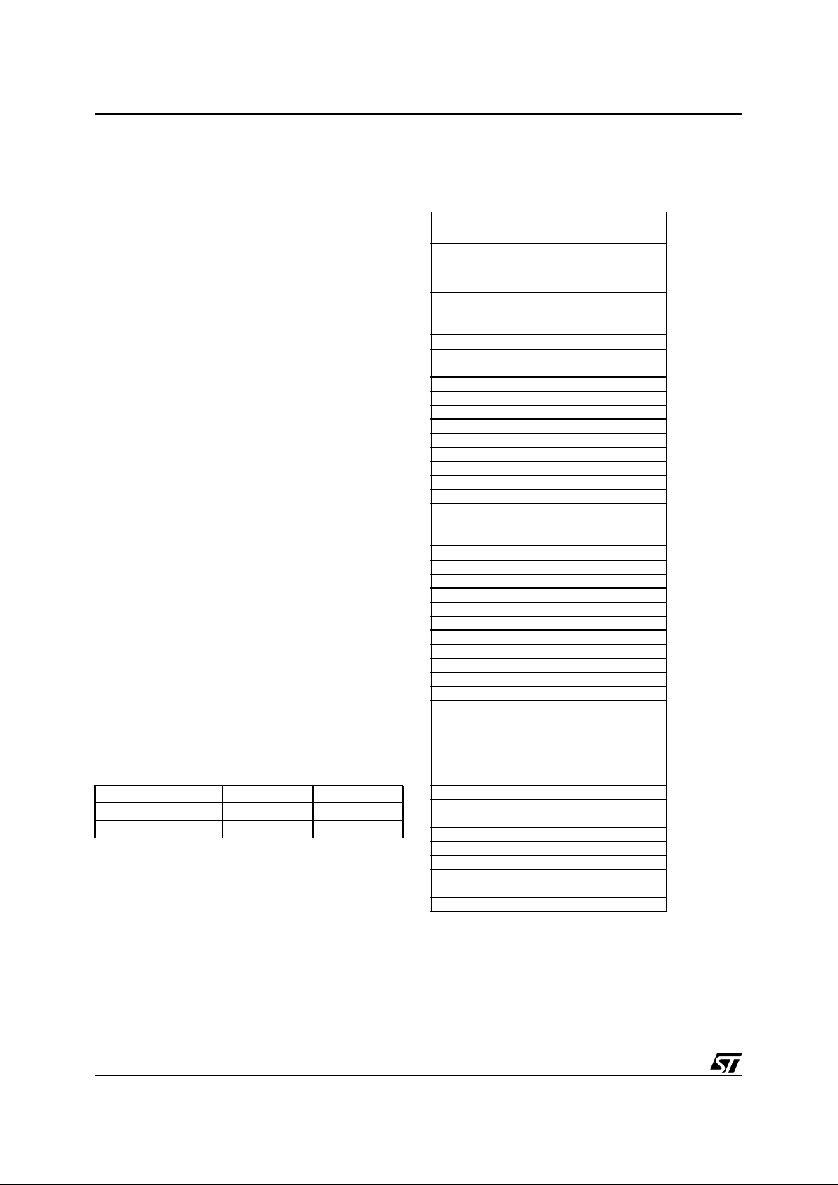
The ST62T52B and ST62T62B devices is low cost
members of the ST62xx 8-bit HCMOS family of
microcontrollers, which is targeted at low to medium complexity applications. All ST62xx devices
are based on a bui lding block approach: a common core is surrounded by a number of on-chip
peripherals.
The ST62E62B is the erasable EPROM version of
the ST62T62B device, which may be used t o em ulate the ST62T52B and ST62T62B devices as
well as the ST6252B and ST6262B ROM devices.
OTP and EPROM dev ices are functionally identical. The ROM based versions offer the same functionality selecting as ROM options the options de-
fined in the programmable option byte of the
OTP/EPROM versions.
OTP devices of f er al l the advantages of us er programmability at low cost, which make them the
ideal choice in a wide range of applications where
frequent code changes, m ultiple code versions or
last minute programmability are required.
These compact low-cost devices feature a Tim er
comprising an 8-bit counter and a 7-bit programmable prescaler, an 8-bit Auto-Reload Timer,
EEPROM data capability (except ST62T52 B), an
8-bit A/D Converter with 4 analog inputs and a
Digital Watchdog timer, making them well suited
for a wide range of automot ive, appliance and industrial applications.
Figure 1. Bloc k D ia gram
TEST
NMI
INTERRUPT
PROGRAM
PC
STACK LEVEL 1
STACK LEVEL 2
STACK LEVEL 3
STACK LEVEL 4
STACK LEVEL 5
STACK LEVEL 6
POWER
SUPPLY
OSCILLATOR
RESET
DATA ROM
USER
SELECTABLE
DATA RAM
PORT A
PORT B
TIMER
DIGITAL
8 BIT CORE
TEST/V
PP
8-BIT
A/D CONVERTER
PA4..PA5 / Ain
PB0, PB2..PB3 / 20 mA Sink
V
DDVSS
OSCin OSCout RESET
WATCHDOG
MEMORY
PB6 / ARTimin / 20 mA Sink
PORT C
PC2..PC3 / Ain
AUTORELOAD
TIMER
PB7 / ARTimout / 20 mA Sink
128 Bytes
1836 bytes OTP
(ST62T52B, T62B)
1836 bytes EPROM
(ST62E62B)
DATA EEPROM
64 Bytes
(ST62T62B/E62B)
4
Page 5

5/68
ST62T52B ST62T62B/E62B
1.2 PIN DESCRIPTIONS
V
DD
and V
SS
. Power is supplied to the MCU via
these two pins. V
DD
is the power connection and
VSS is the ground connection.
OSCin and OSCout.
These pins are internally
connected to the on-chip oscillator circuit. A quartz
crystal, a ceramic resonator or an exte rnal clock
signal can be connected between these two pins.
The OSCin pin is the input pin, the OSCout pin is
the output pin.
RESET
. The active-low RESET pin is used to re-
start the microcontroller.
TEST/V
PP
.
The TEST m ust be held at V
SS
for normal operation. If TEST pin is connected to a
+12.5V level during the reset phase, the
EPROM/OTP programming Mode is entered.
NMI.
The NMI pin provides the capability for asynchronous interruption, by applying an external non
maskable interrupt to the MCU. The NMI input is
falling edge sensitive. It is provided with an onchip pullup resistor and Schmitt trigger characteristics.
PA4-P A5 .
These 2 lines are organized as one I/O
port (A). Each line may be configured under software control as inputs with or without internal pullup resistors, interrupt generating in puts with pullup resistors, open-drain or push-pull outputs, analog inputs for the A/D converter.
PB0, PB2-PB3, PB6-PB7.
These 5 lines are organized as one I/O port (B). Each line may be configured under software control as inputs with or
without internal pull-up resistors, interrupt generating inputs with pull-up resistors, open-drain or
push-pull outputs. PB6/ARTIMin and PB7/ARTI-
Mout are either Port B I/O bits or the Input and
Output pins of the ARTimer.
Reset state of PB2-PB3 pins can be defined by
option either with pull-up or high impedance.
PB0, PB2-PB3, PB6-PB7 scan also sink 20mA for
direct LED driving.
PC2-PC3
. These 2 lines are organized as one I/O
port (C). Each line may be configured under software control as inpu t with or without internal pul lup resistor, interrupt generating input with pull-up
resistor, analog input for the A/D convert er, opendrain or push-pull output.
Figure 2. ST62T52B, E62B and T62B Pin
Configuration
1
2
3
4
5
6
7
89
10
11
12
13
14
15
16
PB0
V
PP
/TEST
PB2
PB3
V
DD
ARTIMin/PB6
PC2/Ain
PC3/Ain
PA5/Ain
PA4/Ain
ARTIMout/PB7
V
SS
NMI
RESET
OSCout
OSCin
5
Page 6

6/68
ST62T52B ST62T62B/E62B
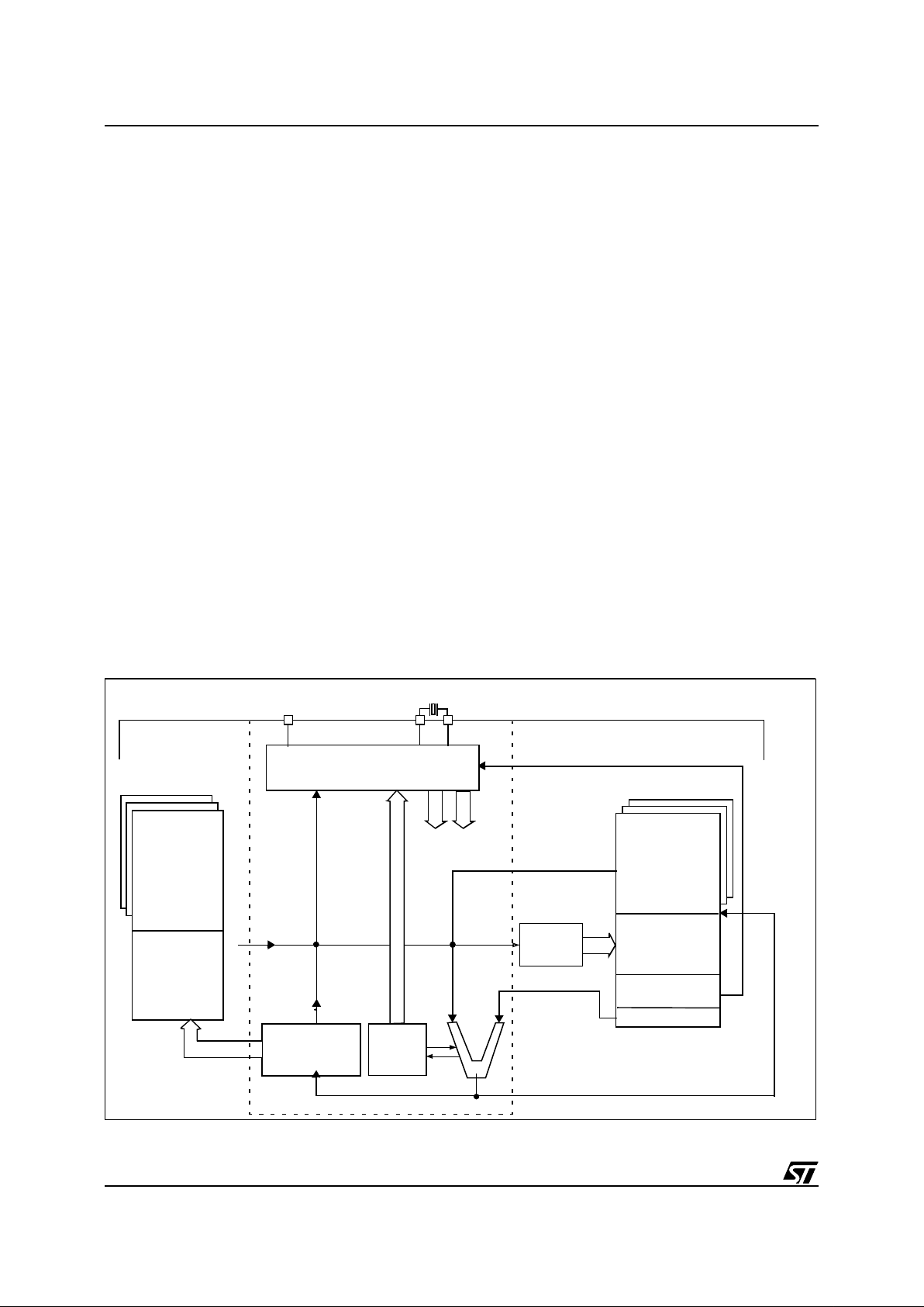
1.3 MEMORY MAP
1.3.1 Introduction
The MCU operates in three separate memory
spaces: Program space, Data space, and Stack
space. Operation in these three memory spaces is
described in the following paragraphs.
Briefly, Program space contains user program
code in OTP and user vectors; Data space c ontains user data in RAM and in OTP, and Stack
space accommodat es six levels of stack for subroutine and interrupt service routine nesting.
Figure 3. Me m ory A ddressing D iagram
PROGRAM SPACE
PROGRAM
INTERRUPT &
RESET VECTORS
ACCUMULATOR
DATA RAM
BANK SELECT
WINDOW SELECT
RAM
X REGISTER
Y REGISTER
V REGISTER
W REGISTER
DATA READ-ONLY
WINDOW
RAM / EEPROM
BANKING AREA
000h
03Fh
040h
07Fh
080h
081h
082h
083h
084h
0C0h
0FFh
0-63
DATA SPACE
0000h
0FF0h
0FFFh
MEMORY
MEMORY
DATA READ-ONL Y
MEMORY
6
Page 7

7/68
ST62T52B ST62T62B/E62B
MEMORY MAP
(Cont’d)
1.3.2 Program Space
Program Space comprises the instructions to be
executed, the data required for immediate addressing mode instructions, the reserved factory
test area and the user vectors. Program Space is
addressed via the 12-bit Program Counter register
(PC register).
1.3.2.1 Program Memory Protection
The Program Memory in O TP or EP ROM dev ices
can be protected against external readout of
memory by selecting the READOUT PROTECTION option in the option byte.
In the EPROM parts, READOUT PROTECTION
option can be disactivated only by U.V. erasure
that also results into the whole EPROM context
erasure.
Note:
Once the Readout Protection is activated, it
is no longer poss ible, even for SGS-THOM SON,
to gain access to the OTP contents. Returned
parts with a protecti on set can therefore not be accepted.
Figure 4. ST62T52B/T62B Program
Memory Ma p
0000h
RESERVED
*
USER
PROGRAM MEMORY
(OTP/EPROM)
1836 BYTES
0F9Fh
0FA0h
0FEFh
0FF0h
0FF7h
0FF8h
0FFBh
0FFCh
0FFDh
0FFEh
0FFFh
RESERVED
*
RESERVED
INTERRUPT VECTORS
NMI VECTOR
USER RESET VECTOR
(*) Reserved areas should be filled with 0FFh
0880h
087Fh
7
Page 8
8/68
ST62T52B ST62T62B/E62B
MEMORY MAP
(Cont’d)
1.3.3 Data Space
Data Space accommodates all the data necessary
for processing the user program. This space comprises the RAM res ource, the processor c ore and
peripheral registers, as well as read-only data
such as constants and look-up tables in
OTP/EPROM.
1.3.3.1 Data ROM
All read-only data is physical ly stored in program
memory, which also accommoda tes the Program
Space. The program m emory consequently contains the program code to be executed, as well as
the constants and look -up tables required by the
application.
The Data Space locations in which the different
constants and look-up tables are addressed by
the processor core may be thought of as a 64-byte
window through which it is possible to access the
read-only data stored in OTP/EPROM.
1.3.3.2 Data RAM/EEPROM
In ST62T52B, T62B and ST62E 62B devices, the
data space includes 60 bytes of RAM, the accumulator (A), the indirect registers (X), (Y), the
short direct registers (V), (W), the I/O port registers, the peripheral data an d cont rol reg isters, the
interrupt option register and the Data ROM Window register (DRW register).
Additional RAM and EEPROM pages can also be
addressed using banks of 64 bytes located between addresses 00h and 3Fh.
1.3.4 Stack Space
Stack space consists of six 12-bit registers which
are used to stack subro utine and interrupt return
addresses, as well as the current program counter
contents.
Table 1. Additional RAM / EEPROM Banks
Table 2. ST62T52B, T62B and ST62E62B Data
Memory Space
Device RAM EEPROM
ST62T52B 1 x 64 bytes ST62T62B 1 x 64 bytes 1 x 64 bytes
RAM / EEPROM banks
000h
03Fh
DATA ROM WINDOW AREA
040h
07Fh
X REGISTER 080h
Y REGISTER 081h
V REGISTER 082h
W REGISTE R 083h
DATA RAM 60 BYTES
084h
0BFh
PORT A DATA REGISTE R 0C0h
PORT B DATA REGISTE R 0C1h
PORT C DATA REGISTER 0C2h
RESERVED 0C3h
PORT A DIRECTION REGISTER 0C4h
PORT B DIRECTION REGISTER 0C5h
PORT C DIRECTION REGISTER 0C6h
RESERVED 0C7h
INTERRUPT OPTION REGISTER 0C8h*
DATA ROM WINDOW REGISTER 0C9h*
RESERVED
0CAh
0CBh
PORT A OPTION RE GI STER 0CCh
PORT B OPTION RE GI STER 0CDh
PORT C OPTION REGISTER 0CEh
RESERVED 0 CFh
A/D DATA REGISTER 0D0h
A/D CONT RO L REGISTE R 0D1h
TIMER PRESCALER REGISTER 0D2h
TIMER COUNTER REGISTER 0D3h
TIMER STATUS CONTROL REGIST ER 0D4h
AR TIMER MODE CONTROL REGISTER 0D5h
AR TIMER STATUS/CONTROL REGISTER1 0D6h
AR TIMER STATUS/CONTROL REGISTER2 0D7h
WATCHDOG REGISTER 0D8h
AR TIMER RELOAD/CAPTURE REGISTE R 0D9h
AR TIMER COMPARE REGISTER 0DAh
AR TIMER LOAD REGISTER 0DBh
OSCILLATOR CONTROL REGISTER 0DCh*
MISCELLANEOUS 0DDh
RESERVED
0DEh
0E7h
DATA RAM/EEPROM REGISTER 0E8h*
RESERVED 0E9h
EEPROM CONTROL REGISTER 0EAh
RESERVED
0EBh
0FEh
ACCUMULATOR 0FFh
* WRITE ONLY REGIST ER
8
Page 9

9/68
ST62T52B ST62T62B/E62B
MEMORY MAP
(Cont’d)
1.3.5 Data Window Register (DWR)
The Data read-only memory window is located
from address 0040h to address 007Fh in Data
space. It allows direct reading of 64 consec utive
bytes located anywhere in program memory, between address 0000h and 0FFFh (top memory address depends on the specific device). All the program memory can therefore be used to store either
instructions or read-only data. Indeed, the window
can be moved in steps of 64 b ytes along t he program memory by writing the appropriate code in the
Data Window Register (DWR).
The DWR can b e addressed like any RAM location in the Data Spac e, it is howev er a write-only
register and therefore cannot be accessed using
single-bit operations. This register is used to position the 64-byte read-only data window (from address 40h to address 7Fh of the Data space) in
program memory in 64-byte steps. The ef fective
address of the byte to be read as data in program
memory is obtained by concatenating the 6 least
significant bits of the register address given in t he
instruction (as least significant bits) and the content of the DWR register (as most significant bits),
as illustrated in Figure 5 below. For instance,
when addressing location 0040h of the Data
Space, with 0 loaded in the DWR register, the
physical location addressed in program memory is
00h. The DWR register is not cleared on reset,
therefore it must be written to prior to the first access to the Data read-only memory window area.
Data Window Register (DWR)
Address: 0C9h — Write Only
Bits 6, 7 = Not used.
Bit 5-0 =
DWR5-DWR0:
Data read-only memory
Window Register Bits.
These are the Data readonly memory Window bits that correspond to the
upper bits of the data read-only memory space.
Caution:
This register is undef ine d o n res et. Ne ither read nor single bit instructions may be used to
address this register.
Note:
Care is required when ha ndling the DWR
register as it is write only. For this reason, the
DWR contents should not be changed while executing an interrupt service routine, as the service
routine cannot save and then restore the register’s
previous contents. If it is impossible to a void writing to the DWR during the interrupt service routine, an image o f the register must be saved in a
RAM location, and each time the program writes
to the DWR, it must also write to the image register. The image register must be written first so
that, if an interrupt occurs between the two i nstructions, the DWR is not affected.
Figure 5. Data read-only memory Window Memo ry Add ressi ng
70
- - DWR5 DWR4 DWR3 DWR2 DWR1 DWR0
DATA ROM
WINDOW REGISTER
CONTENTS
DATA SPACE ADDRESS
40h-7Fh
IN INSTRUCTION
PROGRAM SPACE ADDRESS
765432 0
543210
543210
READ
1
67891011
0
1
VR01573C
12
1
0
DATA SPACE ADDRESS
:
:
59h
000
0
1
00
1
11
Example:
(DWR)
DWR=28h
11
0000000
1
ROM
ADDRESS:A19h
11
13
0
1
9
Page 10

10/68
ST62T52B ST62T62B/E62B
MEMORY MAP
(Cont’d)
1.3.6 Data RAM/EEPROM Bank Register
(DRBR)
Address: E8h — Write only
Bit 7-5 = These bits are not used
Bit 4 -
DRBR4
. This bit, when set, selects RAM
Page 2.
Bit 1-3. Not used
Bit 0.
DRBR0
. This bit, when set, selects EEP-
ROM page 0.
The selection of the bank is made by program-
ming the Data RAM Bank Switch register (DRBR
register) located at address E8h of the Data
Space according to Table 1. No more than one
bank should be set at a time.
The DRBR register can be addressed like a RAM
Data Space at the address E8h; nevert heless it is
a write only register that cannot be accessed with
single-bit operations. This register is used to select the desired 64-byte RAM bank of the Data
Space. The number of banks has to be loaded in
the DRBR register and the instruction has to point
to the selected location as if it was in bank 0 (from
00h address to 3Fh address).
This register is not cleared during the MCU initialization, therefore it must be written before the first
access to the Data Space bank region. Refer to
the Data Space description for additional information. The DRBR register is not modified when an
interrupt or a subroutine occurs.
Notes
:
Care is required when handling the DRBR register
as it is write only. For this reason, it is not allowed
to change the DRBR contents whi le executing interrupt service routine, as the service routine cannot save and then restore its previous content. If it
is impossible to avoid the writing of this register in
interrupt service routine, an image of this register
must be saved in a RAM lo cation, and each time
the program writes to DRBR it must write also to
the image register. The image register must be
written first, so if an interrupt occurs between the
two instructions the DRBR is not affected.
In DRBR Regis ter, only 1 bit must be set. Ot herwise two or more pages are enabled in parallel,
producing errors.
Table 3. Data RAM Bank Register Set-up
70
---
DRBR
4
---
DRBR
0
DRBR ST62T52B ST62T62B
00 None None
01 Not available EEPROM page 0
02 Not Available Not Available
08 Not available Not available
10h RAM Page 2 RAM Page 2
other Reserved Reserved
10
Page 11

11/68
ST62T52B ST62T62B/E62B
MEMORY MAP
(Cont’d)
1.3.7 EEPROM Description
EEPROM memory is located in 64-byte pages in
data space. This memory may be used by the user
program for non-volatile data storage.
Data space from 00h to 3Fh is paged as described
in Table 4 . Ro w Arrangement for Pa rallel W riting
of EEPROM Locations. EEPROM locations are
accessed directly by addressing these paged sections of data space.
The EEPROM does not require dedicated instructions for rea d or write access. Once selected via the
Data RAM Bank Register, the active EEPROM
page is controlled by the EEPROM Control Re g ister (EECTL), which is described below.
Bit E20FF of the EECTL register must be reset prior
to any write or read access to the EE PR OM. If no
bank has been selected, or if E2OFF is set, any access is meaningless.
Programming must be enabled by setting the
E2ENA bit of the EECTL register.
The E2BUSY bit of the EECTL register is set when
the EEPROM is performing a program ming cycle.
Any access to the EEPR O M wh en E2BU SY is set
is meaningless.
Provided E2OFF and E2BUSY are reset, an EEPROM location is read just like any other data location, also in terms of access time.
Writing to the EEPROM may be carried out in two
modes: Byte Mode (BMODE) and Parallel Mode
(PMODE). In BMODE, one byte is acc essed at a
time, while in PMOD E up to 8 bytes in the same
row are programmed simultaneously (with consequent speed and power consumption advantages,
the latter being particularly important in battery
powered circuits).
General Notes
:
Data should be written directly to the intended address in EEPROM space. There is no buffer memory between data RAM and the EEPROM space.
When the EEPROM is busy (E2BUSY = “1”)
EECTL cannot be accessed in write mode, it is
only possible to read t he s tatus of E 2BUSY . This
implies that as long a s the EEPROM is busy, it is
not possible to change the status of the EEPROM
Control Register. EECTL bits 4 and 5 are reserved
and must never be set.
Care is required when dealing with the EECTL register, as some bits are write onl y . For this reason,
the EECTL contents must not be altered while executing an interrupt service routine.
If it is impossible to avoid writing to this register
within an interrupt service routine, an image of the
register must be saved in a RAM location, and
each time the program writes to EECTL it must
also write to the image register. T he image re gister must be written to first so that, if an interrupt occurs between the two instructions, the EECT L will
not be affected.
Table 4. . Row Arrang emen t for Para llel Writing of EEPRO M Locations
Dataspace
addresses.
Banks 0 and 1.
Byte01234567
ROW7 38h-3Fh
ROW6 30h-37h
ROW5 28h-2Fh
ROW4 20h-27h
ROW3 18h-1Fh
ROW2 10h-17h
ROW1 08h-0Fh
ROW0 00h-07h
Up to 8 bytes in each row may be programmed simultaneously in Parallel Write mode.
The number of available 64-byte banks (1 or 2) is device dependent.
11
Page 12

12/68
ST62T52B ST62T62B/E62B
MEMORY MAP
(Cont’d)
Additional Notes on Parallel Mode:
If the user wishes to perform parallel programming, the first step should be to set the E2PAR2
bit. From this time on, the EEPROM will be addressed in write mode, the ROW address will be
latched and it will be possible to chan ge it only at
the end of the programming cycle, or by resetting
E2PAR2 without programming the EEPROM. After the ROW address is latched, the MCU can only
“see” the selected EEPROM row a nd any atte mpt
to write or read other rows will produce errors.
The EEPROM should not be read while E2PAR2
is set.
As soon as the E2 PAR2 bit is set, the 8 volatile
ROW latches are cleared. From this moment on,
the user can load data in all or in part of the ROW.
Setting E2PAR1 will modify the EEPROM registers corresponding to the ROW latches acces sed
after E2PAR2. For example, if the software sets
E2PAR2 and a cce sse s the EEPROM by wr i ting to
addresses 18h, 1Ah and 1Bh, and then sets
E2PAR1, these three registers will be modified simultaneously; the remaining bytes in the row will
be unaffected.
Note that E2PAR2 is internally reset at t he en d of
the programming cycle. This implies that the user
must set the E2PAR2 bit between two parallel programming cycles. Note that if the user tries to set
E2PAR1 while E2PAR2 is not set, there will be no
programming cycle and the E2PAR1 bit will be unaffected. Consequently, the E2PAR1 bit cannot be
set if E2ENA is low. The E2PAR1 bit can be set by
the user, only if the E2ENA and E2PAR2 bits are
also set.
EEPROM Control Regi s t e r (EEC T L)
Address: EAh — Read/Write
Reset status: 00h
Bit 7 = D7:
Unused.
Bit 6 =
E2OFF
:
Stand-by Enable Bit.
WRIT E ON LY.
If this bit is set the EEPROM is disabled (any access
will be meaningless) and the power consumption of
the EEPROM is reduced to its lowest value.
Bit 5-4 =
D5-D4
:
Reserved.
MUST be kept reset.
Bit 3 =
E2PAR1
:
Parallel Start Bit.
WRITE ONLY.
Once in Parallel Mode, as soon as the user software
sets the E2PAR1 bit, parallel writing of the 8 adjacent registers will start. This bit is internally reset at
the end of the programm ing procedure. Not e that
less than 8 bytes can be written if required, the undefined bytes being unaffected by the parallel programming cycle; this is explained in greater detail
in the Additional Notes on Parallel Mode overleaf.
Bit 2 =
E2PAR2
:
Parallel Mode En. Bit.
WRITE
ONLY. This bit must be set by the user program in
order to perform parallel programming. If E2PAR2
is set and the parallel start bit (E2PAR1) is reset,
up to 8 adjacent bytes can be written simultaneously. These 8 adjacent bytes are considered as a
row, whose addres s lines A7, A6, A5, A 4, A3 are
fixed while A2, A1 and A0 are the chan ging bits,
as illustrated in Table 4. E2PAR2 is automatical ly
reset at the end of any parallel progra mming procedure. It can be reset by the user software before
starting the programming procedure, thus leaving
the EEPROM registers unchanged.
Bit 1 =
E2BUSY
:
EEPROM Busy Bit.
READ ONLY. This bit is automatically set by the EEPROM
control logic when the EEPROM is in programming mode. Th e user program should test it before any EEPROM read or write operation; any attempt to access the EEPRO M while the busy bit is
set will be aborted and the writing procedure in
progress will be completed.
Bit 0 =
E2ENA
:
EEPROM Enable Bit.
WRITE ONLY. This bit enables programming of the EEPROM
cells. It must be s et before any write to the EEPROM register. Any attempt to write to the EEPROM when E2ENA i s low is m eanin gless and will
not trigger a write cycle.
70
D7
E2O
FF
D5 D4
E2PAR1E2PAR2E2BUSYE2E
NA
12
Page 13

13/68
ST62T52B ST62T62B/E62B
1.4 PROGRAMMING MODES
1.4.1 Option Byte
The Option B yte all o ws conf igurat ion capability to
the MCUs. Option byte’s content is automatically
read, and the selected options enabled, whe n the
chip reset is activated.
It can only be acces sed during the programming
mode. This access is made either automatically
(copy from a master device) or by selecting the
OPTION BYTE PROGRAMMING mode of the
programmer.
The option byte is located in a non-user map. No
address has to be specified.
EPROM Code Option Byte
PROTECT
. This bit allows the protection of the
software contents against piracy. When the bit
PROTECT is se t high, readout of the OTP contents is prevented by hardware. No programming
equipment is able to gain access to the user program. When this bit is low, the user program can
be read.
EXTCNTL
. This bit selects the External STOP
Mode capability. When EXTCNTL is high, pin NMI
controls if the STOP mode can be accessed when
the watchdog is active. When EXTCNTL is low,
the STOP instruction is processed as a WAIT as
soon as the watchdog is active.
PB2- 3 P UL L
. When set this bit removes pull-up at
reset on PB2-PB3 pins. When cleared PB2-PB3
pins have an internal pull-up resistor at reset.
D4
. Reserved. Must be cleared to zero.
WDACT
. This bit controls the watchdog activation.
When it is high, hardware activation is sel ected.
The software activation is sel ected when W D AC T
is low.
DELAY
. This bit enables the selection of the delay
internally generated after pin RESET is released.
When DELAY is low, the delay is 2048 cycles of
the oscillator, it is of 32768 cycles when DELAY is
high.
OSCIL
. When this bit is low, the oscillator must be
controlled by a quartz crystal, a ceramic resonator
or an external frequency. When it is high, the oscillator must be controlled by an RC ne twork, with
only the resistor having to be externally provided.
D0
. Reserved. Must be cleared to zero.
The Option byte is written during programming either by using t he PC menu (PC driven Mode) or
automatically (stand-alone mode)
1.4.2 Program Memory
EPROM/OTP programming mode is set by a
+12.5V voltage appl ied to the TE ST/V
PP
pin. The
programming flow of the ST62T62B is described
in the User Manual of the EP ROM Programming
Board.
The MCUs can be programmed with the
ST62E6xB EPROM programming tools available
from SGS-THOMS ON.
Table 5. ST62T52B/T62B Program Memory Map
Note
: OTP/EPROM dev ices can be programme d
with the development tools available from
SGS-THOMSON (ST62E6X-EPB or
ST626X-KIT).
1.4.3 . EEPROM Data Memory
EEPROM data pages are supplied in the virgin
state FFh. Partial or total programming of EEPROM data memory can be performed either
through the application software or through an external programmer. Any SGS-THOMSON tool
used for the program memory (OTP/EPROM) can
also be used to program the EEPROM data memory.
70
PROTECT
EXTC-
NTL
PB2-3
PULL
- WDACT DELAY OSCIL -
Device Address Description
0000h-087Fh
0880h-0F9Fh
0FA0h-0FEFh
0FF0h-0FF7h
0FF8h-0FFBh
0FFCh-0FFDh
0FFEh-0FFFh
Reserved
User ROM
Reserved
Interrupt Vectors
Reserved
NMI Interrupt Vector
Reset Vector
13
Page 14
14/68
ST62T52B ST62T62B/E62B
2 CENTRAL PR OCESSING UNIT
2.1 INTRODUCTION
The CPU Core of ST6 devices is independent of
the I/O or Memory configuration. As such, it may be
thought of as an independent central processor
communicating with on-chip I/O, M emory and Peripherals via internal address, data, and control
buses. In-core communication is arranged as
shown in Figure 6; the controller being externally
linked to both the Reset and Oscillator circuits,
while the core is linked to the dedicated on-chip peripherals via the serial data bus and indirectly, for
interrupt purposes, through the control registers.
2.2 CPU REGISTERS
The ST6 Family CPU core features six registers and
three pairs of flags available to the programmer.
These are described in the following paragraphs.
Accumulator (A)
. The accumulator is an 8-bit
general purpose register used in all arithmetic calculations, logical operations, and data manipulations. The accumulator can be addressed in Data
space as a RAM l ocation at address FFh. Thus
the ST6 can manipulate the ac cumulator just like
any other register in Data space.
Indirect Registers (X, Y).
These two indirect registers are used as pointers to memory locations in
Data space. They are used i n the regist er-indirect
addressing mode. These registers can be addressed in the data space as RAM locations at addresses 80h (X) and 81h (Y). They can also be accessed with the direct, short direct, or bit direct addressing modes. Accordingly, the ST6 instruction
set can use the indirect registers as any other register of the data space.
Short Direct Registers (V, W).
These two registers are used to save a byte in short direct addressing mode. T hey can be addressed in Data
space as RAM locations at addresses 82h (V) and
83h (W). They can also be accessed using the direct and bit direct addressing modes. Thus, the
ST6 instruction set can use the sho rt direct registers as any other register of the data space.
Program Counter (PC). The program cou nter is a
12-bit register which contains the address of the
next ROM location to be process ed by the core.
This ROM location may be an opcode, an operand, or the address of an operand. The 12-bit
length allows the direct addressing of 4096 bytes
in Program space.
Figure 6ST6 Core Block Diagram
PROGRAM
RESET
OPCODE
FLAG
VALUES
2
CONTROLLER
FLAGS
ALU
A-DATA
B-DATA
ADDRESS/READ LINE
DATA SPACE
INTERRUPTS
DATA
RAM/EEPROM
DATA
ROM/EPROM
RESULTS TO DATA SPACE (WRITE LINE)
ROM/EP ROM
DEDICA T I ONS
ACCUMULATOR
CONTRO L
SIGNALS
OSCin
OSCout
ADDRESS
DECODER
256
12
Program Co unter
and
6 LAYER STACK
0,01 TO 8MHz
VR01811
14
Page 15

15/68
ST62T52B ST62T62B/E62B
CPU REGISTERS
(Cont’d)
However, if the program space contains more
than 4096 bytes, the additional memory in program space can be address ed by using the Program Bank Switch register.
The PC value is incremented after reading the address of the current instruction. To execute relative jumps, the PC and the offset are shifted
through the ALU, where they are added; the result
is then shifted back into the PC. The program
counter can be changed in the following ways:
- JP (Jump) instructionPC=Jump address
- CALL instructionPC= Call address
- Relative Branch Instruction.PC= PC +/- offset
- Interrupt PC=Interrupt vector
- ResetPC= Reset vector
- RET & RETI instructionsPC= Pop (stack)
- Nor mal in structio nPC= PC + 1
Flags (C, Z)
. The ST6 CPU includes three pairs of
flags (Carry and Zero), each pair being associated
with one of the three normal modes of operat ion:
Normal mode, Interrupt mode and Non Maskable
Interrupt mode. Each pair consists of a CARRY
flag and a ZERO flag. One pair (CN, ZN) is used
during Normal operation, another pair is used during Interrupt mode (CI, ZI), and a third pair is used
in the Non Maskable Interrupt mode (CNMI, ZNMI).
The ST6 CPU uses the pair of flags associated
with the current mode: as soon a s an in terrupt (or
a Non Maskable Interrupt) is generated, the ST 6
CPU uses the Interrupt flags (resp. the NMI flags)
instead of the Normal flags. When the RETI instruction is executed, the previously used set of
flags is restored. It should be no ted tha t eac h flag
set can only be addressed in its own context (Non
Maskable Interrupt, Normal Interrupt or M ain routine). The flags are not cleared during context
switching and thus retain their status.
The Carry flag is set when a carry or a borrow occurs during arithmetic operations; otherwise it is
cleared. The Carry flag is al so set to the value of
the bit tested in a bit test instruction; it also participates in the rotate left instruction.
The Zero flag is set if the result of the last arithmetic or logical operation was equal to zero; otherwise it is cleared.
Switching between the three sets of flags is performed automatically when an NMI, an interrupt or
a RETI instructions occurs. As the NMI mode is
automatically selected after the reset of the M CU,
the ST6 core uses at first the NMI flags.
Stack.
The ST6 CPU includes a true LIFO hardware stack which elim inates the need for a stack
pointer. The stack consists of six separate 12-bit
RAM locations that do not belong to the data
space RAM area. When a subroutine call (or in terrupt request) occurs, the contents of each level
are shifted into the next higher level, while the
content of the PC is shifted into the first level (the
original contents of the sixth stack level are lost).
When a subroutine or interrupt return occurs (RET
or RETI instructions), the first level register is shifted back into the PC and the value o f each le vel is
popped back into the previous level. Since the accumulator, in common with all other data space
registers, is not stored in this stack, management
of these registers should be performed within the
subroutine. The st ack will remain in its “deepest”
position if more than 6 nested calls or interrupts
are executed, and consequently the last return address will be lost. It will also remain in its highest
position if the stack is empty and a RET or RETI is
executed. In this case the next instruction will be
executed.
Figure 7ST6 CPU Programmi ng Mode
l
SHORT
DIRECT
ADDRESSING
MODE
VREGISTER
WREGISTER
PROGRAM COUNTER
SIX LEVELS
ST ACK REGI STER
CZNORMAL FLAGS
INTERRUPT FLAGS
NMI FLAGS
INDEX
REGISTER
VA 000423
b7
b7
b7
b7
b7
b0
b0
b0
b0
b0
b0b11
ACCUMULATOR
Y R EG. POINTER
X R EG. POINTER
CZ
CZ
15
Page 16

16/68
ST62T52B ST62T62B/E62B
3 CLOCKS, RESET, INTER RUPTS AND POWER SAVIN G MO DES
3.1 CLOCK SYSTEM
The MCU features a Main Oscillator which can be
driven by an external clock, or used in conjunction
with an AT-cut parallel resonant crystal or a suitable ceramic resonator, or with an external resistor
(R
NET
).
Figure 8. illustrates various possible oscillator con-
figurations using an external crystal or ceramic resonator, an external clock input, an external resistor
(R
NET
). CL1 an CL2 should have a capacitance in the
range 12 to 22 pF for an oscillator frequency in the
4-8 MHz range.
A programmable divider is provided in order to adjust
the internal clock of the MCU to the best power consumption and performance trade-off.
The internal MCU clock frequency (f
INT
) drives directly the AR TIMER while it is divided by 12 to
drive the TIMER, the A/D converter and the
Watchdog timer, and by 13 to drive the CPU core,
as may be seen in Figure 9..
With an 8MHz oscillator frequency, the fastest
machine cycle is therefore 1.625µs.
A machine cycle is the smal lest unit of time needed
to execute any operation (for instance, to increment
the Program Counter). An inst ruction m ay req uire
two, four, or five machine cycles for execution.
3.1.1 Main Oscillator
The oscillator configuration may be specified by selecting the appropriate option. When the CRYSTAL/RESONATOR option is selected, it must be
used with a quartz crystal, a cerami c resonat or or
an external signal provided on the OSCin pin. When
the RC NETWORK option is selected, the system
clock is generated by an external resistor.
Figure 8. Oscillator Configurations
OSC
in
OSC
out
C
L1n
C
L2
ST6xxx
CRYSTAL/RESO NATOR CL O CK
CRYSTAL/RESONATOR option
OSC
in
OSC
out
ST6xxx
EXTERNAL CLOCK
CRYSTAL/RESONATOR option
NC
OSC
in
OSC
out
R
NET
ST6xxx
RC NETWORK
RC NETW O RK option
NC
16
Page 17

17/68
ST62T52B ST62T62B/E62B
CLOCK SYSTEM
(Cont’d)
Oscillator Control Registers
Address: DCh — Write only
Bit 7-4. These bits are not used.
Bit 3. Reserved. Cleared at Reset. THIS BIT
MUST BE SET TO 1 BY USER PROGRAM to
achieve lowest power consumption.
Bit 2. Reserved. Must be kept low.
RS1-RS0. These bits select the division ratio of
the Oscilla tor Divide r in order to genera te the internal frequency. The following selctions are available:
Note
: Care is required when handling the OSCR
register as some bits are wri te only. For this reason, it is not allowed to change the OSCR contents while executing interrupt service rout ine, as
the service routine cannot save and t hen restore
its previous content. If it is impossible to avoid the
writing of this register in inte rrupt service routine,
an image of this register mus t be s aved i n a RA M
location, and each time the program writes to
OSCR it must write also to the image register. The
image register must be writte n first, so if an interrupt occurs between the two instructions the
OSCR is not affected.
Figure 9. Clo ck Cir c ui t Block Diagram
70
----
OSCR3OSCR
2
RS1 RS0
RS1 RS0 Division Ratio
0
0
1
1
0
1
0
1
1
2
4
4
MAIN
OSCILLATOR
Core
:
13
:
12
:
1
Timer
Watchdog
POR
f
INT
ADC
AR Timer
OSCILLATOR
DIVIDE R
RS0, RS1
OSCin
OSCout
f
OSC
f
OSC
17
Page 18

18/68
ST62T52B ST62T62B/E62B
3.2 RESETS
The MCU can be reset in three ways:
– by the external Reset input being pulled low;
– by Power-on Reset;
– by the digital Watchdog peripheral timing out.
3.2.1 RESET Input
The RESET
pin may be c onnected to a device of
the application board in order to reset t he M CU if
required. The RESET
pin may be pulled low in
RUN, WAIT or STOP mode. This input can be
used to reset the MCU internal state and ensure a
correct start-up procedure. The pin is ac tive low
and features a Schmitt trigger input. The i nternal
Reset signal is generated by adding a delay to the
external signal. Therefore even short pulses on
the RESET
pin are acceptable, p rovided VDD has
completed its rising phase and that the oscillator is
running correctly (normal RUN or WAIT modes).
The MCU is kept in the Reset state as long as the
RESET
pin is held low.
If RESET
activatio n occ urs in the RU N or WAIT
modes, processing of the user program is stopped
(RUN mode only), the Inputs and Outputs are configured as inputs with pull-up resistors and the
main Oscillator is restarted. When the level on the
RESET pin then goes high, the initialization sequence is executed following expiry of the internal
delay period.
If RESET
pin activation occurs in the STOP mode,
the oscillator starts up and all I nputs and O utputs
are configured as inputs with pull-up resistors.
When the level of the RESET
pin then goes high,
the initialization sequence is executed following
expiry of the internal delay period.
3.2.2 Power-on Reset
The function of the POR circuit consists in waking
up the MCU at an appropriate stage during the
power-on sequence. At the beginning of this sequence, the MCU is configured in the Reset state:
all I/O ports are configured as inputs with pull-up
resistors and no instruction is executed. When the
power supply voltage rises to a sufficient level, the
oscillator starts to operate, whereupon an inte rnal
delay is initiated, in order to allow the oscillator to
fully stabilize before executing the first instruction.
The initialization sequence is executed immediately following the internal delay.
The internal delay is generated by an on-chip counter. The internal reset line is released 2048 internal
clock cycles after release of the external reset.
Notes:
To ensure correct start-up, the user shou ld take
care that the reset signal is not released before
the V
DD
level is su ffic ient to allow MC U ope ratio n
at the chosen frequ ency (see Rec om me nded O perating Conditions).
A proper reset sig nal f or a s lo w ri sing V
DD
supply
can generally be provided by an external RC network connected to the RESET
pin.
Figure 10. Reset and Interrupt Processing
INT LATCH CLEARED
NMI MASK SET
RESET
( IF PRESENT )
SELECT
NMI MODE FLAGS
IS RESET STILL
PRESENT?
YES
PUT FFEH
ON ADDRESS BUS
FROM RESET LOCATIO NS
FFE/FFF
NO
FETCH INSTRUCTI ON
LOAD PC
VA000427
18
Page 19

19/68
ST62T52B ST62T62B/E62B
RESETS
(Cont’d)
3.2.3 Watchdog Reset
The MCU provides a Watchdog timer function in
order to ensure graceful recovery from software
upsets. If the Watchdog register is not refreshed
before an end-of -count condition is reached, the
internal reset will be activated. This, amongst other things, resets the watchdog counter.
The MCU restarts just as though the Reset had
been generated by the RESET
pin, including the
built-in stabilisation delay period .
3.2.4 Application Notes
No external resistor is required between V
DD
and
the Reset pin, thanks to the built-in pull-up device.
The POR circuit operates dynamically, in that it
triggers MCU init ialization on detec ting the rising
edge of V
DD
. The typical threshold is in the region
of 2 volts, but the actual value of the detected
threshold depends on the way in which V
DD
rises.
The POR circuit is
NOT
designed to supervise
static, or slowly rising or falling V
DD
.
3.2.5 MCU Initialization Sequence
When a reset occurs the s tack is reset, the PC is
loaded with the address of the Reset Vector (located in program ROM starting at address
0FFEh). A jump to the begin ning of the user program must be coded at this address. Fo llowing a
Reset, the Interrupt flag is automatically set, so
that the CPU is in Non Maskable In terrupt mode;
this prevents the initialisation routine from being
interrupted. The initialisation routine should therefore be terminated by a RETI instruction, in order
to revert to normal mode a nd enable interrupts. If
no pending interrupt is present at the end of the initialisation routine, the MCU will continue by
processing the instruction immediately following
the RETI instruction. If, however, a pending interrupt is present, it will be serviced.
Figure 11. Reset and Interrupt Processing
Figure 12. Reset Block Diagram
RESET
RESET
VECTOR
JP
JP:2 BYTES/4 CYCLES
RETI
RETI: 1 BYTE/2 CYCLES
INITIALIZATION
ROUTINE
VA00181
V
DD
RESET
300k
Ω
2.8k
Ω
POWER
WATCHDOG RESET
CK
COUNTER
RESET
ST6
INTERNAL
RESET
f
OSC
RESET
ON RESET
VA0200B
19
Page 20

20/68
ST62T52B ST62T62B/E62B
RESETS
(Cont’d)
Table 6. Register Reset Status
Register Address(es) Status Comment
Oscillator Control Register
EEPROM Control Register
Port Data Registers
Port Direction Register
Port Option Register
Interrupt Option Register
TIMER Status/Control
AR TIMER Mode Control Register
AR TIMER Status/Control 1 Register
AR TIMER Status/Control 2Register
AR TIMER Compare Register
Miscellaneous Register
0DCh
0EAh
0C0h to 0C2h
0C4h to 0C6h
0CCh to 0CEh
0C8h
0D4h
0D5h
0D6h
0D7h
0DAh
0DDh
00h
f
INT
= f
OSC
; user must set bit3 to 1
EEPROM enabled (if available)
I/O are Input with pull-up
I/O are Input with pull-up
I/O are Input with pull-up
Interrupt disabled
TIMER disabled
AR TIMER stopped
X, Y, V, W, Register
Accumulator
Data RAM
Data RAM Page REgister
Data ROM Window Register
EEPROM
A/D Result Register
AR TIMER Load Register
AR TIMER Reload/Capture Register
080H TO 083H
0FFh
084h to 0BFh
0E8h
0C9h
00h to F3h
0D0h
0DBh
0D9h
Undefined
As written if programmed
TIMER Counter Register
TIMER Prescaler Register
Watchdog Counter Register
A/D Control Register
0D3h
0D2h
0D8h
0D1h
FFh
7Fh
FEh
40h
Max count loaded
A/D in Standby
20
Page 21

21/68
ST62T52B ST62T62B/E62B
3.3 DIGITAL WATCHDOG
The digital Watchdog consists of a reloadable
downcounter timer which can be used to provide
controlled recovery from software upsets.
The Watchdog circuit generates a Reset when the
downcounter reaches zero. User software can
prevent this reset by reloading the counter, and
should therefore be written so that the counter is
regularly reloaded while the user program runs
correctly. In the event of a software misha p (usually caused by externally generated interference),
the user program will no longer behave in its usual
fashion and the timer register will thus not be reloaded periodically. Consequently the timer will
decrement down to 00h and reset the MCU. In order to maximise the effectiveness of the Watchdog function, user software must be written with
this concept in mind.
Watchdog behaviour is governed by two options,
known as “WATCHDOG ACTIVATION” (i.e.
HARDWARE or SOFTWARE) and “EXTERNAL
STOP MODE CONTROL” (see Table 7 Recom-
mended Option Choices).
In the SOFTWARE option, the Watchdog is disabled until bit C of the DWDR register has been set.
When the Watchdog is disabled, low power Stop
mode is available. Once activated, the Watchdo g
cannot be disabled, except by resetting the MCU.
In the HARDWARE option, t he Watchdog is permanently enabled. Since the oscillator will run
continuously, low power mode is not available.
The STOP instruction is interpreted as a WAIT instruction, and the Watchdog continues to countdown.
However, when the EXTERNAL STOP MODE
CONTROL option has been selected low power
consumption may be achieved in Stop Mode.
Execution of the STOP instruction is then governed by a secondary function associated with the
NMI pin. If a STOP instruction is encountered
when the NMI pin is low, it is interpreted as WAIT,
as described above. If, however, the STOP instruction is encountered when the NMI pin is high,
the Watchdog counter is frozen and the CPU enters STOP mode.
When the MCU exits STOP mode (i.e. when an interrupt is generated), the Watchdog resumes its
activity.
Table 7. Recommended Option Choices
Functions Required Recommended Options
Stop Mode & Watchdog “EXTERNAL STOP MODE” & “HARDWARE WATCHDOG”
Stop Mode “SOFTWARE WATCHDOG”
Watchdog “HARDWARE WATCHDOG”
21
Page 22

22/68
ST62T52B ST62T62B/E62B
DIGITAL WATCHDOG
(Cont’d)
The Watchdog is associated with a Data space
register (Digital WatchDog Register, DWDR, location 0D8h) which is described in great er detail in
Section 3.3.1 Digital Watchdog Register (DWDR).
This register is set to 0FEh on Reset: bit C is
cleared to “0”, which di sables the Watchdog; the
timer downcounter bits, T0 to T5, and t he SR bit
are all set to “1”, thus selecting the longest Watchdog timer period. Thi s time period can be set t o
the user’s requirements by setting the appropriate
value for bits T0 to T5 in the DWDR register. The
SR bit must be set to “1”, since it is this bit which
generates the Reset signal when it changes to “0”;
clearing this bit would generate an immediate Reset.
It should be noted that the o rder of the bi ts in the
DWDR register is inverted with respect to the associated bits in the down counter: bit 7 of the
DWDR register corresponds, in fact, to T 0 and bit
2 to T5. The user should bear in mind the fact that
these bits are inverted and shifted with respect to
the physical counter bits when writing to this register. The relationship between the DWDR register
bits and the physical implementation of the Watchdog timer downcounter is illustrated in Figure 13..
Only the 6 most significant bits may be used to define the time period, since it is b it 6 which triggers
the Reset when it changes to “0”. This offers the
user a choice of 64 timed periods ranging from
3,072 to 196,608 clock cycles (with an oscillator
frequency of 8 MHz, this is equivalent to timer periods ranging from 384µs to 24.576ms).
Figure 13. Watchdog Counter Co nt rol
WATCHDOG CONTROL REGISTER
D0
D1
D3
D4
D5
D6
D7
WATCHDOG COUNTER
C
SR
T5
T4
T3
T2
T1
D2
T0
OSC ÷12
RESET
VR02068A
÷
2
8
22
Page 23

23/68
ST62T52B ST62T62B/E62B
DIGITAL WATCHDOG
(Cont’d)
3.3.1 Digital Watchdog Register (DWDR)
Address: 0D8h — Read/Write
Reset status: 1111 1110b
Bit 0 = C:
Watchdog Control bit
If the hardware option is selected, this bit is forced
high and the user cannot change it (the Watchdog
is always active). When the softw are opt ion is selected, the Watchdog function is ac tivated by setting bit C to 1, and cannot then be disabled (save
by resetting the MCU).
When C is kept l ow t he co unter c an be used as a
7-bit timer.
This bit is cleared to “0” on Reset.
Bit 1 = SR:
Software Reset bit
This bit triggers a Reset when cleared.
When C = “0” (Watchdog disabled) it is the MSB of
the 7-bit timer.
This bit is set to “1” on Reset.
Bits 2-7 =
T5-T0
:
Downcounter bits
It should be noted that the register bits are reversed and shifted with respect to the physical
counter: bit-7 (T0) is the LSB of the Watchdog
downcounter and bit-2 (T5) is the MSB.
These bits are set to “1” on Reset.
3.3.2 Application Notes
The Watchdog plays an important s upporting role
in the high noise immunity of ST62xx devices, and
should be used wherever possible. Watchdog related options should be selecte d on th e basis of a
trade-off between appl ication security and ST OP
mode availability.
When STOP mod e is not requi red, h ardware act ivation without EXTERNAL STOP MODE CONTROL should be preferred, as it provides maximum security, especially during power-on.
When STOP m ode is required, hardware act ivation and EXTERNAL STOP MODE CONTROL
should be chosen. NMI sho uld be h igh by def aul t,
to allow STOP mode to be entered when the MCU
is idle.
The NMI pin c an be c onn ec ted to an I/O line (see
Figure 14.) to allow its state to be controlled by
software. The I/O line can then be used to keep
NMI low while Watchdog protection is required, or
to avoid noise or key bounce. When no more
processing is required, the I/O line is released and
the device placed in STOP mode for lowest power
consumption.
When software activation is selected and the
Watchdog is not activated, the dow ncounter may
be used as a simple 7-bit timer (remember that the
bits are in reverse order).
The software activation option should be chosen
only when the Watchdog c ou nter is to be used as
a timer. To ensure the Watchdog has not been unexpectedly activated, the following instructions
should be executed within the first 27 instructions:
jrr 0, WD, #+3
ldi WD, 0FDH
70
T0 T1 T2 T3 T4 T5 SR C
23
Page 24

24/68
ST62T52B ST62T62B/E62B
DIGITAL WATCHDOG
(Cont’d)
These instructions test the C bit and Reset the
MCU (i.e. disable the Watchdog) if the bit is set
(i.e. if the Watchdog is active), thus disabling t he
Watchdog.
In all modes, a minimum of 28 instructions are executed after activation, before the Watchdog can
generate a Reset. Consequently, user software
should load the watchdog counter within the first
27 instructions following Watchdog activation
(software mode), or within the f irst 27 instructions
executed following a Reset (hardware activation).
It should be noted that when the GEN bit is low (interrupts disabled), the NMI interrupt is active but
cannot cause a wake up from STOP/WAIT
modes.
Figure 14. A typical circuit making use of the
EXERNAL STOP MODE CONTROL feature
Figure 15. Digital Watchdog Block Diagram
NMI
SWITCH
I/O
VR02002
RSFF
8
DATA BUS
VA00010
-2
-12
OSCILLATOR
RESET
WRITE
RESET
DB0
R
S
Q
DB1.7 SETLOAD
7
8
-2
SET
CLOCK
24
Page 25

25/68
ST62T52B ST62T62B/E62B
3.4 INTERRUPTS
The CPU can manage four Maskable Interrupt
sources, in addition to a Non Maskable Interrupt
source (top priority interrupt). Each source is associated with a specific Interrupt Vector which
contains a Jump inst ruction to the associated interrupt service routine. These vectors are located
in Program space (see Table 8 Interrupt Vector
Map).
When an interrupt source generates an interrupt
request, and interrupt processing is enabled, the
PC register is loaded with the address of the interrupt vector (i.e. of the Jump instruction), which
then causes a Jump to the relevant interrupt service routine, thus servicing the interrupt.
Interrupt sources are linked to events either on external pins, or on chip peripherals. Several events
can be ORed on the same in terrupt source, and
relevant flags are available to determine which
event triggered the interrupt.
The Non Maskable Interrupt request has the highest priority and can interrupt any interrupt routine
at any time; the other four interrupts cannot in terrupt each other. If more than one interrupt request
is pending, these a re proces sed by the processor
core according to their priority level: source #1 has
the higher priority while source #4 the lower. The
priority of each interrupt source is fixed.
Table 8. Interrupt Vector Map
3.4.1 Interrupt request
All interrupt sources but the Non Maskable Interrupt source can be disabled by setting accordingly
the GEN bit of the Interrupt Option Register (IOR).
This GEN bit also defines if an interrupt source, including the Non Maskable Interrupt source, can
restart the MCU from STOP/WAIT modes.
Interrupt request from the Non Maskable Interrupt
source #0 is latched by a flip flop which is automatically reset by the core at the beginning of the
non-maskable interrupt service routine.
Interrupt request from source #1 can be configured either as ed ge or level sensitive by setting
accordingly the LES bit of the Interrupt Option
Register (IOR).
Interrupt request from s ource #2 are always edge
sensitive. The edge p olarity can be configu red by
setting accord ing ly the ESB bit o f th e Inte rr upt Option Register (IOR).
Interrupt request from sources #3 & #4 are level
sensitive.
In edge sensitive mode, a latch is set when a edge
occurs on the interrupt source line and is cleared
when the associated interrupt routine is started.
So, the occurrence of an interrupt can be stored,
until completion of the running interrupt routine before being processed. If several interrupt requests
occurs before completion of the running interrupt
routine, only the first request is stored.
Storage of interrupt requests is not available in
level sensitive mode. To be taken into account,
the low level must be present on the interrupt pin
when the MCU samples the line after instruction
execution.
At the end o f ev ery inst ruction, the M CU t ests the
interrupt lines: if there is a n interrupt request the
next instruction is not executed and the appropriate interrupt service routine is executed instead.
Table 9. Interrupt Option Register Description
Interrupt Source Priority Vector Address
Interrupt source #0 1 (FFCh-FFDh)
Interrupt source #1 2 (FF6h-FF7h)
Interrupt source #2 3 (FF4h-FF5h)
Interrupt source #3 4 (FF2h-FF3h)
Interrupt source #4 5 (FF0h-FF1h)
GEN
SET Enable all interrupts
CLEARED Disable all interrupts
ESB
SET
Rising edge mode on interrupt source #2
CLEARED
Falling edge mode on interrupt source #2
LES
SET
Level-sensitive mode on interrupt source #1
CLEARED
Falling edge mode on interrupt source #1
OTHERS NOT USED
25
Page 26

26/68
ST62T52B ST62T62B/E62B
IINTERRUPTS
(Cont’d)
3.4.2 Interrupt Procedure
The interrupt procedure is very similar to a call
procedure, indeed the user can consider the interrupt as an asynchronous call procedure. As this is
an asynchronous event, the user cannot know the
context and the time at which it occurred. As a result, the user should save all Data space registers
which may be used within the interrupt routines.
There are separate sets of processor flags for normal, interrupt and non-maskable interrupt modes,
which are automatically switched and so do not
need to be saved.
The following list summarizes the interrupt procedure:
MCU
– The interrupt is detected.
– The C and Z flags are replaced by the interrupt
flags (or by the NMI flags).
– The PC contents are stored in the first level of
the stack.
– The normal interrupt lines are inhibited (NMI still
active).
– The first internal latch is cleared.
– The associated interrupt vector is loaded in the PC.
WARNING:
In some circumstances, when a
maskable interrupt occurs while the ST6 core is in
NORMAL mode an d e specially during t he execution of an "ldi IOR, 00h" instruction (disabling all
maskable interrupts): if the interrupt arrives during
the first 3 cycles of the "ldi" instruction (which is a
4-cycle instruction) the core will switch to interrupt
mode BUT the flags CN and ZN will NOT switch to
the interrupt pair CI and ZI.
User
– User selected registers are saved within the in-
terrupt service routine (normally on a software
stack).
– The source of the interrupt is found by polling the
interrupt flags (if more than one source is asso-
ciated with the same vector).
– The int e rrupt is serviced.
– Return from interrupt (RETI)
MCU
– Automatically the MCU switches back to the nor-
mal flag set (or the interrupt flag set) and pops
the previous PC value from the stack.
The interrupt routine usually begins by the identifying the device which generated the interrupt request (by polling). The user should save the registers which are used within the interrupt routine in a
software stack. After the RETI instruction is executed, the MCU returns to the main routine.
Figure 16. Interrupt Processing Flow Chart
INSTRUCTION
FETCH
INSTRUCTION
EXECUTE
INSTRUCTION
WAS
THE INSTRUCTION
A RETI
?
?
CLEAR
INTERRUPT MASK
SELECT
PROGRAM FLAGS
"POP"
THE STACKED PC
?
CHECK IF THERE IS
AN INTERRUPT REQUEST
AND INTERRUPT MASK
SELECT
INTERNAL MODE FLAG
PUSH THE
PC INTO THE STACK
LOAD PC FROM
INTERRUPT VECTOR
(FFC/FFD)
SET
INTERRUPT MASK
NO
NO
YES
IS THE CORE
ALREADY IN
NORMAL MODE?
VA000014
YES
NO
YES
26
Page 27

27/68
ST62T52B ST62T62B/E62B
IINTERRUPTS
(Cont’d)
3.4.3 Interrupt Option Register (IOR)
The Interrupt Option Register (IOR) is used to enable/disable the individual interrupt sources and to
select the operating mode of the external interrupt
inputs. This register is write-only and cannot be
accessed by single-bit operations.
Address: 0C8h — Write Only
Reset status: 00h
Bit 7, Bits 3-0 =
Unused
.
Bit 6 =
LES:
Level/Edge Selection bit
.
When this bit is set to one, the interrupt source #1
is level sensitive. When cleared to zero the e dge
sensitive mode for interrupt request is selected.
Bit 5 =
ESB
:
Edge Selection bit
.
The bit ESB selects the polarity of the interrupt
source #2.
Bit 4 =
GEN
:
Global Enable Interrupt
. When this
bit is set to one, all interrupts are ena bled. When
this bit is cleared to zero all the interrupts (excluding NMI) are disabled.
When the GEN bit is low, the NMI interrupt is active but cannot cause a wake up from STOP/WAIT
modes.
This register is cleared on reset.
3.4.4 Interrupt Sources
Interrupt sources available on the
ST62E62B/T62B are summarized i n the Table 10
with associated mask bit to enab le/disable the interrupt request.
Table 10. Interrupt Requests and Mask Bits
70
- LES ESB GEN - - - -
Peripheral Register
Address
Register
Mask bit Masked Interrupt Source
Interrupt
vector
GENERAL IOR C8h GEN
All Interrupts, excluding NM
I
TIMER TSCR1 D4h ETI TMZ: TIMER Overflow Vector 4
A/D CONVERTER ADCR D1h EAI EOC: End of Conversion Vector 4
AR TIMER ARMC D5h
OVIE
CPIE
EIE
OVF: AR TIMER Overflow
CPF: Successful compare
EF: Active edge on ARTIMin
Vector 3
Port PAn ORPA-DRPA C0h-C4h ORPAn-DRPAn PAn pin Vector 1
Port PBn ORPB-DRPB C1h-C5h ORPBn-DRPBn PBn pin Vector 1
Port PCn ORPC-DRPC C2h-C6h ORPCn-DRPCn PCn pin Vector 2
27
Page 28

28/68
ST62T52B ST62T62B/E62B
INTERRUPTS
(Cont’d)
Figure 17. Interrupt Block Diagram
Start
1
I
Q
CLK
CLR
FF
1
0
MUX
IOR REG. C8H, bit 6
IOR REG. C8H, bit 5
FF
CLR
CLK
Q
I
2
Start
TIMER1
CPIE
CPF
TMZ
ETI
INT #4 (FF0,1)
INT #3 (FF2,3)
INT #2 (FF4,5)
INT #1 (FF6,7)
RESTART FROM
STOP/WAIT
AR TIMER
EF
EIE
OVF
OVIE
VA0426P
PBE
Bits
Bits
PORT B
PORT A
PBE
PBE
DD
V
SINGLE BIT ENABLE
FROM REGISTER PORT A,B,C
PORT C
Start
0
I
Q
CLK
CLR
FF
Bit GEN (IOR Register)
NMI (FFC,D)
NMI
V
DD
ADC
EOC
EAI
28
Page 29

29/68
ST62T52B ST62T62B/E62B
3.5 POWER SAVING MODES
The WAIT and STOP modes have been implemented in the ST62xx family of MCUs in order to
reduce the product’s elect rical consumption during idle periods. These two p ower saving modes
are described in the following paragraphs.
3.5.1 WAIT Mode
The MCU goes into WA IT mode as soon as the
WAIT instruction is executed. Th e microc ontroller
can be considered as being in a “sof tware froz en”
state where the core stops processing the program instructions, the RAM content s and peripheral registers are preserved as long as the power
supply voltage is higher than the RAM retention
voltage. In this mode t he peripherals are still active.
WAIT mode can b e used when the u ser wants t o
reduce the MCU po wer consumption during idle
periods, while not losing track of time or the capability of mon it o rin g e x t er na l ev e nt s . T h e a c tive o s cillator is not stopped i n order to provide a c lock
signal to the peripherals. Timer counting may be
enabled as well as th e T im er interrupt, before entering the WAIT mode: this allows the WAIT mode
to be exited when a Timer interrupt occurs. The
same applies to other p eripherals which use the
clock signal.
If the WAIT mode is exited due t o a Reset (either
by activating the externa l pin or generated by the
Watchdog), the MCU enters a normal reset procedure. If an interrupt is generated during WAIT
mode, the MCU’s behaviour depends on the state
of the processor core prior to the WAIT instruction,
but also on the kind of interrupt request which is
generated. This is described in the following paragraphs. The processor core does no t generate a
delay following the occurrence of the interrupt, because the oscillator clock is still available and no
stabilisation period is necessary.
3.5.2 STOP Mode
If the Watchdog is disabled, STO P mode is available. When in STOP m ode, the MC U is placed in
the lowest power consumption mode. In this operating mode, the microcontroller can be considered
as being “frozen”, no instruction is executed, the
oscillator is stopped, the RAM contents and peripheral registers are preserved as long as the
power supply voltage is higher than the RAM retention voltage, and the ST62xx core waits for the
occurrence of an external interrupt request or a
Reset to exit the STOP state.
If the STOP st ate is exited due to a Res et (by activating t he ex ter na l p in) the MCU will ent e r a no rmal reset procedure. Behaviour in response to interrupts depends on the state of the processor
core prior to issuing the STOP instruction, and
also on the kind of i nterrupt re quest that is generated.
This cas e will be d escribed in the follow ing par agraphs. The processor core gene rates a delay after occurrence of the interrupt request, in order to
wait for complete stabilisation of the oscillator, before executing the first instruction.
29
Page 30

30/68
ST62T52B ST62T62B/E62B
POWER SAVING MODE
(Cont’d)
3.5.3 Exit from WAIT and STOP Modes
The following paragraphs describe how the M CU
exits from WAIT and STOP modes, when an interrupt occurs (not a Reset). It should be noted that
the restart sequence depends on the original state
of the MCU (normal, interrupt or non-maskable interrupt mode) prior to entering WAIT or STOP
mode, as well as on the interrupt type.
Interrupts do not affect the oscillator selection.
3.5.3.1 Normal Mode
If the MCU was in the main routine when the WAIT
or STOP instruction was executed, exit from Stop
or Wait mode will occur as soon as an interrupt occurs; the related interrupt routine is executed and,
on completion, the instruction which follows the
STOP or WAIT instruction is then exec uted, providing no other interrupts are pending.
3.5.3.2 Non Maskable Interrupt Mode
If the STOP or WAIT instruction has been executed during execution of the non-maskable interrupt
routine, the MCU exits from the Stop or Wait mode
as soon as an interrupt occurs: the instruction
which follows the STOP or WAIT instruction is executed, and the MCU remains in non-maskable interrupt mode, even if an other interrupt has been
generated.
3.5.3.3 Normal Interrupt Mode
If the MCU was in interrupt mode before the STOP
or WAIT instruction was executed, it exits from
STOP or WAIT mode as soon as an interrupt occurs. Nevertheless, two cases must be considered:
– If the interrupt is a normal one, the interrupt rou-
tine in which the W AIT or STO P mode wa s en-
tered will be completed, starting with the
execution of the instruction which follows the
STOP or the WAIT instruction, and the MCU is
still in the interrupt mode. At the end of this routine pending interrupts will be serviced in accordance with their priority.
– In the event of a non-maskable interrupt, the
non-maskable interrupt service routine is processed first, then the routine in which the WAIT or
STOP mode was entered will be comp leted by
executing the instruction following the STOP or
WAIT instruction. The MCU remains in normal
interrupt mode.
Notes:
To achieve the lowest power consumption durin g
RUN or WAIT modes, the user program must take
care of:
– configuring unused I/Os as inputs without pull-up
(these should be externally tied to well defined
logic levels);
– placing all peripherals in their power down
modes before entering STOP mode;
When the hardware activated Watchdog is selected, or when the software Watchdog is enabled,
the STOP instruction is disabled and a WA IT instruction will be executed in its place.
If all interrupt sources are disabled (GEN low), the
MCU can only be res tarted by a Reset. Althoug h
setting GEN low does not ma sk the NM I as an i nterrupt, it will stop it generating a wake-up signal.
The WAIT and S TOP instructions are no t executed if an enabled interrupt request is pending.
30
Page 31

31/68
ST62T52B ST62T62B/E62B
4 ON-CHIP PER IPHERALS
4.1 I/O PORTS
The MCU features Input/Output lines which may
be individually programmed as any of the following input or output configurations:
– Input without pull-up or interrupt
– Input with pull-up and interrupt
– Input with pull-up, but without interrupt
– Analog input
– Push- pull output
– Open drain output
The lines are organised as bytewise Ports.
Each port is associated with 3 registers in Data
space. Each bit of these registers is associated
with a particular line (for i nstance, bits 0 of Port A
Data, Direction and Option registers are a ssociated with the PA0 line of Port A).
The DATA registers (DRx), are used to read the
voltage level values of t he lines which hav e been
configured as inputs, or to write the logic value of
the signal to be output on the lines configured as
outputs. The port data registers can be read to get
the effective logic levels of the pins, but they c an
be also written by user software, in conjunction
with the related option registers, to select the different input mode options.
Single-bit operations on I/O registers are poss ible
but care is necessary because reading in input
mode is done from I/O pins while writing will directly affect the Port data register causing an undesired change of the input configuration.
The Data Direction registers (DDRx) allow the
data direction (input or output) of each pin to be
set.
The Option registers (O Rx) are used to select the
different port options available both in input and in
output mode.
All I/O registers can be read or written to just as
any other RAM location in Data space, so no extra
RAM cells are needed for port data storage and
manipulation. During MCU initialization, all I/O
registers are cleared and the input mode with pullups and no interrupt generation is selected for all
the pins, thus avoiding pin conflicts.
Figure 18. I/O Port Block Diagram
V
DD
RESET
SIN CONTROL S
S
OUT
SHIFT
REGISTER
DATA
DATA
DIRECTION
REGISTER
REGISTER
OPTION
REGISTER
INPUT/OUTPUT
TO INTERRUPT
V
DD
TO ADC
VA00413
31
Page 32

32/68
ST62T52B ST62T62B/E62B
I/O PO R T S
(Cont’d)
4.1.1 Operating Modes
Each pin may be individually programmed as input
or output with various configurations.
This is achieved by writing the relevant bit in the
Data (DR), Data Direction (DDR) and Option registers (OR). Table 11 I/O Port Option Selection illustrates the various port configurations which can
be selected by user software.
4.1.1.1 Input Options
Pull-up, High Impedance Option. All input lines
can be individually programmed with or without an
internal pull-up by programming the OR and DR
registers accordingly. If the pull-up option is not
selected, the input pin will be in the high-impedance state.
4.1.1.2 Interrupt Options
All input lines can be individually connected by
software to the interrupt system by programming
the OR and DR registers accordingly. The interrupt trigger modes (f alling edge, rising edge and
low level) can be configured by software as described in the Interrupt Chapter for each port.
4.1.1.3 Analog Input Options
Some pins can b e c onf igured as anal og i nput s by
programming the OR and DR registers accordingly. These analog inputs are connected to the onchip 8-bit Analog to Digital Converter.
ONLY ONE
pin should be program med as an ana log input at
any time, since by selecting more than one input
simulta neously their pins will be effec tively short ed.
Table 11. I/O Port Option Selection
Note:
X = Don’t care
DDR OR DR Mode Option
0 0 0 Inp ut With pull-u p, no interrupt
0 0 1 Input No pull-up, no interrupt
0 1 0 Input With pull-up and with interrupt
0 1 1 Input Analog input (when available)
1 0 X Output Open-drain output (20mA sink when available)
1 1 X Output Push-pull output (20mA sink when available)
32
Page 33

33/68
ST62T52B ST62T62B/E62B
I/O PO R T S
(Cont’d)
4.1.2 Safe I/O State Switching Sequence
Switching the I/O ports from on e state to another
should be done in a sequence which ensures that
no unwanted side effects c an occur. The recommended safe transitions are illustrated in Figure
19.. All other transitions are potentially risky and
should be avoided when changing the I/O ope rating mode, as it is most likely that undesirable sideeffects will be experienced, such as spurious interrupt generation or two pins shorted together by the
analog multiplexer.
Single bit instructions (SET, RES, INC and DEC)
should be used with great caution on Ports Data
registers, since these instructions make an implicit
read and write back of the entire register. In port
input mode, however, the data register reads from
the input pins directly, and not from the data register latches. Since data register information in input
mode is used to set the characteristics of the input
pin (interrupt, pull-up, analog input), these may be
unintentionally reprogrammed depending on the
state of the input pins. As a general rule, it is better
to limit the use of s ingle bit instructions on data
registers to when the whole (8-bit) port is in output
mode. In the case of inputs or of mixed inputs and
outputs, it is advisable to keep a copy of the data
register in RAM. Single bit instructions may then
be used on the RAM c opy, after which the whole
copy register can be written to the port data register:
SET bit, datacopy
LD a, datacopy
LD DRA, a
Warning:
Care must also be taken to not use instructions that act on a whole port register (INC,
DEC, or read operations) when all 8 bits are not
available on t he device. Unavaila ble bits m ust b e
masked by software (AND instruction ).
The WAIT and STOP instructions allow the
ST62xx to be used i n situations where low po wer
consumption is needed. The lowest power consumption is achieved by configuring I/Os in input
mode with well-defined logic levels.
The user must take care not to switch outputs with
heavy loads during the conversion of one of the
analog inputs in order to av oi d any disturbance to
the conversion.
Figure 19. Diagram showing Safe I/O State Transitions
Note *.
xxx = DDR, OR, DR Bits respectively
Interrupt
pull-up
Output
Open Drain
Output
Push-pull
Input
pull-up (Reset
state)
Input
Analog
Output
Open Drain
Output
Push-pull
Input
010*
000
100
110
011
001
101
111
33
Page 34

34/68
ST62T52B ST62T62B/E62B
I/O PO R T S
(Cont’d)
Table 12. I/O Port Option Selections
Note 1
. Provided the correct configurati on has been selected.
MODE AVAILABLE ON
(1)
SCHEMATIC
Input
Reset state(
Reset state if PULL-UP
option disabled
PA4-PA5
PB0, PB6-PB7
PC2-PC3
PB2-PB3,
Input
Reset state
Reset state if PULL-UP
option enabled
PA4-PA5
PB0,,PB6-PB7
PC2-PC3
PB2-PB3
Input
with pull up
with interrupt
PA4-PA5
PB0, PB2-PB3,PB6-PB7
PC2-PC3
Analog Input
PA4-PA5
PC2-PC3
Open drain output
5mA
Open drain output
20mA
PA4-PA5
PC2-PC3
PB0, PB2-PB3,PB6-PB7
Push-pull output
5mA
Push-pull output
20mA
PA4-PA5
PC2-PC3
PB0, PB2-PB3,PB6-PB7
Data in
Interrupt
Data in
Interrupt
Data in
Interrupt
Data out
ADC
Data out
34
Page 35

35/68
ST62T52B ST62T62B/E62B
I/O PO R T S
(Cont’d)
4.1.3 ARTimer alternate functions
When bit PWMOE of register ARMC is low, pin
ARTIMout/PB7 is configured as any standard pin
of port B through the port registers. When PWMOE is high, ARTMout/PB7 is the PWM output,
independently of the port registers configuration.
ARTIMin/PB6 is connected t o the AR Timer inpu t.
It is configured through the port registers as any
standard pin of port B. To use ARTIMin/PB6 as
AR Timer input, it must be configured as input
through DDRB.
Figure 20. Peri pheral Interface Configura tio n of AR Ti m er
AR TIMER
ARTIMin
PWMOE
ARTIMout
DR
PID
DR
1
MUX
0
VR01661G
ARTIMin
ARTIMout
PID
OR
35
Page 36

36/68
ST62T52B ST62T62B/E62B
4.2 TIMER
The MCU features an on-chip Timer peripheral,
consisting of an 8-bit counter with a 7-bit programmable prescaler, giving a maximum count of 2
15
.
Figure 21. shows the Timer Block Diagram. The
content of the 8-bit counter can be read/written in
the Timer/Counter register, TCR, which can be
addressed in Data space as a RAM location at address 0D3h. The state of the 7 -bit prescaler can
be read in the PSC register at address 0D2h. The
control logic device is managed in the TSCR register as described in the following paragraphs.
The 8-bit counter is decrem ent by the output (rising edge) coming from the 7-bit prescaler and can
be loaded and read unde r program control . When
it decrements to zero then the TMZ (Timer Zero)bit in the TSCR is set. If the ET I (Ena ble Timer
Interrupt) bit in the TSCR is also set, an interrupt
request is generated. The Timer interrupt can be
used to exit the MCU from WAIT mode.
The prescaler input is the internal frequency (f
INT
)
divided by 12. The prescaler decrements on the
rising edge. Depending on the division factor programmed by PS2, P S 1 and PS0 bit s in the T S CR
(see Table 13.), t he c lock inpu t of the tim er/co unter register is multiplexed to different sources. For
division factor 1, the clock input of the prescaler is
also that of timer/counter; for factor 2, bit 0 of the
prescaler register is connecte d to the clock input
of TCR. This bit changes its state at half the frequency of the prescaler input clock. For factor 4,
bit 1 of the PS C is co nnecte d t o the c lock i nput of
TCR, and so forth. The prescaler initialize bit, PSI,
in the TSCR register must be set to allow the prescaler (and hence the counter) to start. If it is
cleared, all the prescaler bits are set and the counter is inhibited from counting. The prescaler can
be loaded with any value between 0 and 7Fh, if bit
PSI is set. The prescaler tap is selected by means
of the PS2/PS1/PS0 bits in the control register.
Figure 22. illustrates the Timer’s working principle.
Figure 21. Timer Block Diagram
STATUS/CONTROL
8
TMZ ETI
D5
D4
PSI
PS2
PS1 PS0
REGISTER
8-BIT
1 OF 7
SELECT
INTERRUPT
LINE
/
3
5
6
4
3
2
1
0
PSC
VR02070A
f
INT
b7 b6 b5 b4 b3 b2 b1 b0
8 8
.
12
DATA BUS
.
36
Page 37
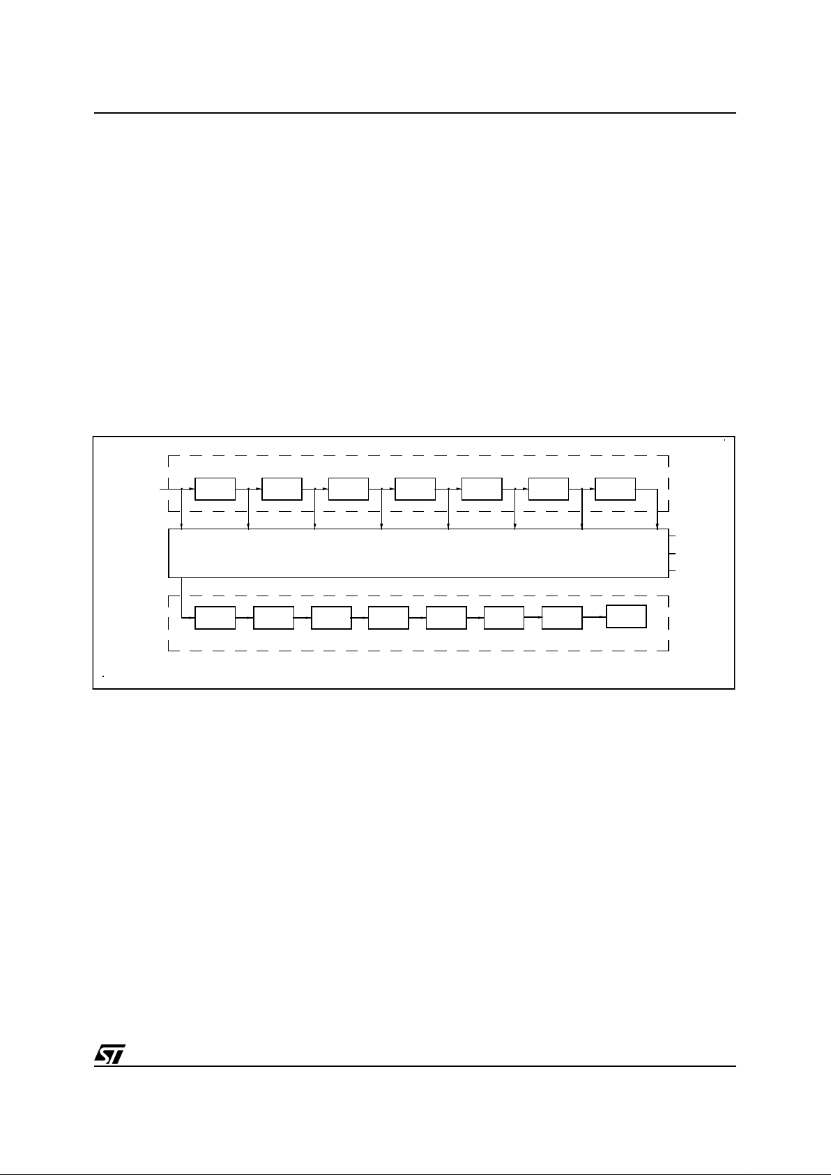
37/68
ST62T52B ST62T62B/E62B
TIMER
(Cont’d)
4.2.1 Timer Operation
The Timer prescaler is clocked by the prescaler
cloc k in put (f
INT
÷ 12).
The user can select the desired prescaler division
ratio through the PS2, PS1, PS0 bits. When the
TCR count reaches 0, it sets the TMZ bit in the
TSCR. The TMZ bit can be tested under program
control to perform a timer function whenever it
goes high.
4.2.2 Timer Interrupt
When the counter register decrements to zero
with the ETI (Enable Timer Interrupt) bit set to one,
an interrupt request associated with Interrupt Vector #3 is generated. When the counter decrements
to ze ro , the TMZ bi t in th e TSC R r egi st er is se t to
one.
4.2.3 Application Notes
TMZ is set wh en the count er reaches zero; h owever, it may also be se t by writing 0 0h in the T C R
register or by setting bit 7 of the TSCR register.
The TMZ bit must be cleared by user software
when servicing the tim er interrupt to avoid undesired interrupts when leaving the interrupt service
routine. After reset, the 8-bit counter register is
loaded with 0FFh, while the 7-bit prescaler is loaded with 07Fh, an d the TSCR register is cleared.
This means that the Timer is stopped (PSI=“0”)
and the timer interrupt is disabled.
Figure 22. Tim e r Working Pri nci pl e
BIT0 BIT1 BIT2
BIT3 BIT6BIT5BIT4
CLOCK
7-BIT PR ESCALER
8-1 MULTIPLEXER
8-BIT COUNTER
BIT0 BIT1
BIT2
BIT3 BIT4 BIT5
BIT6
BIT7
10
2
34
5
67
PS0
PS1
PS2
VA00186
37
Page 38

38/68
ST62T52B ST62T62B/E62B
TIMER
(Cont’d)
A write to t he TC R regist er will p redomina te over
the 8-bit counter decrement to 00h function, i.e. if
a write and a TCR register decrement to 00h occur
simultaneously, the write will take precedence,
and the TMZ bit is not set unti l the 8-bit counter
reaches 00h again. The values of the TCR and the
PSC registers can be read accurately at any time.
4.2.4 Timer Registers
Timer Status Control Register (TSCR)
Address: 0D4h — Read/Write
Bit 7 =
TMZ
:
Timer Ze r o bit
A low-to-high transition indicates that the timer
count register has decrement to zero. This bit
must be cleared by user software before starting a
new count.
Bit 6 =
ETI
:
Enable Timer Interrup
When set, enables the timer interrupt request
(vector #3). If ETI=0 t he t i mer i nterrupt i s disabled.
If ETI=1 and TMZ=1 an interrupt request is generated.
Bit 5 = D5:
Reserved
Must be set to “1”.
Bit 4 =
D4
Do not care.
Bit 3 =
PSI
:
Prescaler Initialize Bit
Used to initialize the prescaler and inhibit its
counting. When PSI=“0” the prescaler is set to
7Fh and the counter is inhibited. When PSI=“1”
the prescaler is enabled to count downwards. As
long as PSI=“0” both counter and prescaler are
not running.
Bit 2, 1, 0 =
PS2, PS1, PS0
:
Prescaler Mux. Se-
lect.
These bits select the division ratio of the pres-
caler register.
Table 13. Prescaler Division Factors
Timer Counter Register (TCR)
Address: 0D3h — Read/Write
Bit 7-0 =
D7-D0
:
Counter Bits.
Prescaler Register PSC
Address: 0D2h — Read/Write
Bit 7 = D7: Always read as "0".
Bit 6-0 =
D6-D0
: Prescaler Bits.
70
TMZ ETI D5 D4 PSI PS2 PS1 PS0
PS2 PS1 PS0 Divided by
0 0 0 1
0 0 1 2
0 1 0 4
0118
10016
10132
11064
111128
70
D7 D6 D5 D4 D3 D2 D1 D0
70
D7 D6 D5 D4 D3 D2 D1 D0
38
Page 39

39/68
ST62T52B ST62T62B/E62B
4.3 AUTO-RELOAD TIMER
The Auto-Reload Timer (AR Timer) on-chip peripheral consists of an 8-bit timer/counter with
compare and capture/reload cap abilities and of a
7-bit prescaler with a clock multiplexer, enabling
the clock input to be selected as f
INT
, f
INT/3
or an
external clock source. A Mode Control Re gister,
ARMC, two Status Control Registers, ARSC0 and
ARSC1, an output pin, ARTIMout, and an input
pin, ARTIMin, allow the Auto-Reload Timer to be
used in 4 modes:
– Auto-reload (PWM generation),
– Output compare and reload on external event
(PLL),
– Input capture and output compare for time
measurement.
– Input capture and output compare for period
measurement.
The AR Timer can be used to wake the MCU from
WAIT mode either with an internal or with an external clock. It also can be used to wake the MCU
from STOP mode, if used w ith an external clock
signal connected to the A RT IMin pin. A Load register allows the program to read and write the
counter on the fly.
4.3.1 AR Timer Description
The AR COUNTER is an 8-bit up-count er incremented on the input clock’s rising edge. The counter is loaded from the Re Load/Capture Register,
ARRC, for auto-reload or capture operations, as
well as for initialization. Direct access to the AR
counter is not possible; however, by reading or
writing the ARLR load register, it is possible to
read or write the counter’s contents on the fly.
The AR Timer’s input clock can be either the internal clock (from the Oscillator Divider), the internal
clock divided by 3, or the clock signal connected to
the ARTIMin pin. Selection between these clock
sources is effected by suitably programming bits
CC0-CC1 of the ARSC1 register. The output of
the AR Multiplexer feeds the 7-bit programmable
AR Prescaler, ARPSC, which selects one of the 8
available taps of the prescaler, as defined by
PSC0-PSC2 in the AR Mode Control Register.
Thus the division factor of the prescaler can be set
to 2n (where n = 0, 1,..7).
The clock input to the AR counter is enabled by
the TEN (Timer Enable) bit in the ARMC register.
When TEN is reset, the AR counter is stopped and
the prescaler and counter contents are frozen.
When TEN is set, the AR counter runs at the rate
of the selected clock source. The counter is
cleared on system reset.
The AR counter may also be initialized by writing
to the ARLR load reg ister, which also causes an
immediate copy of the value to be placed in the
AR counter, regardless of whether the counter is
running or not. Initialization of the counter, by either method, will also clear the ARPSC register,
whereupon counting will start from a known value.
4.3.2 Timer Operating Modes
Four different operating modes are available for
the AR Timer:
Auto-rel oad Mode with PW M Generation.
This
mode allows a Pulse Width Modulated signal to be
generated on the ARTIMout pin with minimum
Core processing overhead.
The free running 8-bit counter is fed by the prescaler’s output, and is incremented on ev ery rising
edge of the clock signal.
When a counter overflow occurs, the counter is
automatically reloaded with the contents of the
Reload/Capture Register, ARCC, and ARTIMout
is set. When the counter reaches the value contained in the compare register (ARCP), ARTIMout
is reset.
On overflow, the OVF flag of t he ARSC0 register
is set and an overflow interrupt request is generated if the overflow interrupt enable bit, OVIE, in the
Mode Control Register (ARMC), is set. The OV F
flag must be reset by the user software.
When the counter reaches the compare value, the
CPF flag of the A RS C0 regi ster i s s et and a compare interrupt request is generated, if the Compare Interrupt e nable b it, CP IE, i n the M ode Control Register (ARMC), is set. T he interrupt service
routine may then adju st the PWM period by lo ading a new value into ARCP. The CPF flag must be
reset by user software.
The PWM signal is generated on the ARTIMout
pin (refer to the Block Diagram). The frequency of
this signal is controlled by the prescaler setting
and by the auto-reload v alue present in the Reload/Capture register, ARRC. The duty cycle of
the PWM signal is controlled by the Compare
Register, ARCP.
39
Page 40

40/68
ST62T52B ST62T62B/E62B
AUTO-RELOAD TIMER
(Cont’d)
Figure 23. . AR Timer Block Diagram
DATA BUS
8
8
8
COMPARE
8
RELOAD/CAPTURE
DATA BUS
AR TIMER
VR01660A
8
8
R
S
TCLD
OVIE
PWMOE
OVF
LOAD
ARTIMout
M
SYNCHRO
ARTIMin
SL0-SL1
INT
f
PB6/
AR
REGISTER
EF
REGISTER
LOAD
AR
U
X
f
INT
/3
AR PRESCALER
7-Bit
CC0-CC1
AR COUNTER
8-Bit
AR COMPARE
REGISTER
OVF
EIE
EF
INTERRUPT
CPF
CPIE
CPF
DRB7
DDRB7
PB7/
PS0-PS2
88
40
Page 41

41/68
ST62T52B ST62T62B/E62B
AUTO-RELOAD TIMER
(Cont’d)
It should be noted th at the reload v alues wi ll also
affect the value and the resolution of the duty cycle of PWM output signal. To obtain a signal on
ARTIMout, the contents of the ARCP register
must be greater than t he contents of the ARRC
regi ster.
The maximum available resolution for the ARTIMout duty cycle is:
Resolution = 1/[255-(ARRC)]
Where ARRC is the content of the Reload/Capture
register. The compare v alue loaded in the Compare Register, ARCP, must be in t he range from
(ARRC) to 255.
The ARTC counter is initialized by writing to the
ARRC register and by then setting the TCLD (Timer Load) and the TEN (Timer Clock Enable) bits in
the Mode Control register, ARMC.
Enabling and selection of th e clock source is controlled by the CC0, CC1, SL0 and SL1 bits in the
Status Control Register, ARSC1. The prescaler division ratio is selected by the PS0, PS1 and PS2
bits in the ARSC1 register.
In Auto-reload Mode, any of the three available
clock sources can be selected: Internal Cl ock, Internal Clock divided by 3 or the clock signal
present on the ARTIMin pin.
Figure 24. . Auto-reload Timer PWM Function
COUNTER
COMPARE
VALUE
RELOAD
REGISTER
PWM OUTPUT
t
t
255
000
VR001852
41
Page 42

42/68
ST62T52B ST62T62B/E62B
AUTO-RELOAD TIMER
(Cont’d)
Capture Mode with PWM Generation
. In this
mode, the AR counter operates as a free runni ng
8-bit counter fed by the prescaler output. The
counter is incremented on every clock rising edge.
An 8-bit capture operation fr om the c ounter t o t he
ARRC register is performed on every active edge
on the ARTIMin pin, when enabled by Ed ge Control bits SL0, SL1 in t he ARSC1 register. At the
same time, the External Flag, EF, in the ARSC0
register is set and an external interrupt request is
generated if the External Interrupt Enable bit, EIE,
in the ARMC register, is set. The EF flag must be
reset by user software.
Each ARTC overflow sets ARTIMout, while a
match between the counter and ARCP (Com pare
Register) resets ARTIMout and sets the compare
flag, CPF. A compare interrupt request is generated if the related compare interrupt enable bit,
CPIE, is set. A PWM signal is generated on ARTIMout. The CPF flag must be reset by user software.
The frequency of the generated signal is determined by the prescaler setting. The duty cycle is
determined by the ARCP register.
Initialization and reading of the counter a re identical to the auto-reload mode (see previous description).
Enabling and selection of clock sources is controlled by the CC0 and CC1 bits in the AR Status
Control Register, ARSC1.
The prescaler division ratio is selected by programming the PS0, PS1 and PS2 bits in the
ARSC1 Register.
In Capture mode, the allowed clock sources are
the internal clock and the internal clock divided by
3; the external ARTIMin input pin shoul d not be
used as a clock source.
Capture Mode with Reset of co un ter an d p rescal er , and PWM Generation.
This mode is identical to the previous one, with the difference that a
capture condition also resets the counter and the
prescaler, thus allowing easy measurement of the
time between two captures (for input period measurement on the ARTIMin pin).
Load on External Input
. The counter operates as
a free running 8-bit counter fed by the prescaler.
the count is incremented on every clock rising
edge.
Each counter overflow sets the ARTIM out pin. A
match between the counter and A RCP (Compare
Register) resets the ARTIMout pin and sets the
compare flag, CPF. A compare interrupt request is
generated if the related compare interrupt enable
bit, CPIE, is set. A PWM signal is generated on
ARTIMout. The CP F flag must be reset by user
software.
Initialization of the counter is a s described in the
previous paragraph. In addition, if the external ARTIMin input is enabled, an active edge on the input
pin will copy the contents of the ARRC register
into the counter, whether the counter is running or
not.
Notes
:
The allowed AR Timer clock sources are the following:
The clock frequ ency s houl d not b e m odif ied while
the counter is count ing, s i nce t he counter may b e
set to an unpredictable value. For instance, the
multiplexer setting should not be modified while
the counter is counting.
Loading of the counter by any means (by auto-reload, through ARLR, ARRC or by the Core) resets
the prescaler at the same time.
Care should be taken whe n both the Capture interrupt and the Overflow interrupt are us ed. Capture and overflow are asynchronous. If the capture
occurs when the Overflow Interrupt Flag, OVF, is
high (between counter overflow and the flag being
reset by software, in the interrupt routine), the External Interrupt Flag, EF, may be cleared simultaneusly without the interrupt being taken into account.
The solution consists in resetting the O VF flag by
writing 06h in the ARSC0 register. The value of EF
is not affected by this operation. If an interrupt has
occured, it will be processed when the MCU exits
from the interrupt routine (the second interrupt is
latched).
AR Timer Mode Clock Sources
Auto-reload mode f
INT
, f
INT/3
, ARTIMin
Capture mode f
INT
, f
INT/3
Capture/Reset mode f
INT
, f
INT/3
External Load mode f
INT
, f
INT/3
42
Page 43

43/68
ST62T52B ST62T62B/E62B
AUTO-RELOAD TIMER
(Cont’d)
4.3.3 AR Timer Registers
AR Mode Control Register (ARMC)
Address: D5h — Read/Write
Reset status: 00h
The AR Mode Co ntrol Register ARMC is used to
program the different operating modes of the AR
Timer, to enable the clock and to initialize the
counter. It can be read and written to by the Core
and it is cleared on system reset (the A R T imer is
disabled).
Bit 7 =
TLCD
:
Timer Load Bit.
This bit, when set,
will cause the contents of ARRC register to be
loaded into the counter and the contents of the
prescaler register, ARPSC, are cleared in order to
initialize the timer before starting to count. This bit
is write-only and any attempt to read it will yield a
logical zero.
Bit 6 =
TEN
: Timer Clock Enable.
This bit, when
set, allows the timer to count. When cleared, it will
stop the timer and freeze ARPSC and ARTSC.
Bit 5 =
PWMOE
:
PWM Output Enable.
This bit,
when set, enables the P WM output o n the ARTIMout pin. When reset, the PWM output is disabled.
Bit 4 =
EIE
:
External Interrupt Enable.
This bit,
when set, enables th e external interrupt request.
When reset, the external interrupt request is
masked. If EIE is set and t he related flag, EF, in
the ARSC0 register is also set, an interrupt request is generated.
Bit 3 =
CPIE
:
Compare Interrupt Enab le.
This bit,
when set, enables the c ompare inte rrupt request.
If CPIE is reset, the compare interrupt request is
masked. If CPIE is set and the related flag, CPF,
in the ARSC0 register is also set, an interrupt request is generated.
Bit 2 =
OVIE
:
Overflow Interrupt
. This bit, when
set, enables the overflow interrupt request. If
OVIE is reset, the compare interrupt request is
masked. If OVIE is set and the related flag, OVF in
the ARSC0 register is also set, an interrupt request is generated.
Bit 1-0 =
ARMC1-ARMC0
:
Mode Control Bits 1-0
.
These are the operating mode control bits. The
following bit combinations will select the various
operating modes:
AR Timer Status/Control Registers ARSC0 &
ARSC1.
These registers contain the AR Timer
status information bits and also allow the programming of c lock sources, active edge an d p rescaler
multiplexer setting.
ARSC0 register bits 0,1 and 2 contain the interrupt
flags of the AR Timer. These bits are read normally. Each one may be reset by sof tware. Writing a
one does not affect the bit value.
AR Status Control Register 0 (ARSC0)
Address: D6h — Read/Clear
Bits 7-3 =
D7-D3
:
Unused
Bit 2 = EF:
External Interrupt Flag.
This bit is set
by any active edg e on the external ARTIMin i nput
pin. The flag is cleared by writing a zero to the EF
bit.
Bit 1 =
CPF
:
Compare Interrupt Flag.
This b it is s et
if the contents of the counter and the ARCP register are equal. The flag is cleared by writing a zero
to the CPF bit.
Bit 0 =
OVF
:
Overflow Interrupt Flag.
This bit is set
by a transition of the counter from FFh to 00h
(overflow). The flag is cleared by writing a zero t o
the OVF bit.
70
TCLD TEN PWMOE EIE CPIE OVIE ARMC1 ARMC0
ARMC1 ARMC0 Operating Mode
0 0 Auto-reload Mode
0 1 Capture Mode
10
Capture Mode with Reset
of ARTC and ARPSC
11
Load on External Edge
Mode
70
D7 D6 D5 D4 D3 EF CPF OVF
43
Page 44

44/68
ST62T52B ST62T62B/E62B
AUTO-RELOAD TIMER
(Cont’d)
AR Status Control Register 1(ARSC1)
Address: D7h — Read/Write
Bist 7-5 =
PS2-PS0
:
Prescaler Division Selection
Bits 2-0.
These bits determine the Prescaler division ratio. The prescaler itself is not affected by
these bits. The prescaler division ratio is listed in the
following table:
Table 14. . Prescaler Division Ratio Selection
Bit 4 =
D4
:
Reserved
. Must be kept reset.
Bit 3-2 =
SL1-SL0
:
Timer Input Edge Control Bits 1-
0.
These bits control the edge function of the Timer
input pin for external synchronization. If bit SL0 is
reset, edge detection is disabled; if set edge detection is enabled. If bit SL1 i s reset, the AR Timer input
pin is rising edge sensitive; if set, it is falling edge
sens i ti ve.
Bit 1-0 =
CC1-CC0
:
Clock Source Select Bit 1-0.
These bits select the clock source for the AR Timer
through the AR M ultiplexer. The programming of
the clock sources is explained in the following Table
15 . Clock Source Selection.:
Table 15. . Clock Source Selection.
AR Load Register ARLR
. The ARLR load register is used to read or write the ARTC counter register “on the fly” (while it is cou nting). The ARLR
register is not affected by system reset.
AR Load Register (ARLR)
Address: DBh — Read/Write
Bit 7-0 =
D7-D0
:
Load Register Data Bits.
These
are the load register data bits.
AR Reload/Capture Register
. The ARRC reload/capture register is used to hold the auto-reload value which is automatically loaded into the
counter when overflow occurs.
AR Reload/Capture (ARRC)
Address: D9h — Read/Write
Bit 7-0 =
D7-D0
:
Reload/Capture Data Bits
. These
are the Reload/Capture register data bits.
AR Compare Register
. The CP compare register
is used to hold the compare value for the compare
function.
AR Compare Register (ARCP)
Address: DAh — Read/Write
Bit 7-0 =
D7-D0
:
Compare Data Bits
. These are
the Compare register data bits.
70
PS2 PS1 PS0 D4 SL1 SL0 CC1 CC0
PS2 PS1 PS0 ARPSC Division Ratio
0
0
0
0
1
1
1
1
0
0
1
1
0
0
1
1
0
1
0
1
0
1
0
1
1
2
4
8
16
32
64
128
SL1 SL0 Edge Detection
X 0 Disabled
0 1 Rising Edge
1 1 Falling Edge
CC1 CC0 Clock Source
00F
int
01F
int
Divided by 3
1 0 ARTIMin Input Clock
1 1 Reserved
70
D7 D6 D5 D4 D3 D2 D1 D0
70
D7 D6 D5 D4 D3 D2 D1 D0
70
D7 D6 D5 D4 D3 D2 D1 D0
44
Page 45

45/68
ST62T52B ST62T62B/E62B
4.4 A/D CONVERTER (ADC)
The A/D converter peripheral is an 8-bit analog to
digital converter with analog inputs as alternate
I/O functions (the number of which i s device dependent), offering 8-bit resolution with a typical
conversion time of 70us (at an oscilla tor clock frequency of 8MHz).
The ADC converts the input voltage by a process
of successive approximations, using a clock frequency derived from the oscillator with a division
factor of twelve. With an oscillator clock frequency
less than 1.2MHz, conversion accuracy is decreased.
Selection of the input pin is done by configuring
the related I/O line as an analog input via the Option and Data registers (ref er to I/O ports description for additional information). Only o ne I/O line
must be configured as an analog input at any time.
The user must avoid any situation in which more
than one I/O pin is selected as an analog inpu t simultaneously, to avoid device malfunction.
The ADC uses two registers in the data space: the
ADC data conversion register, ADR, which stores
the conversion result, and the ADC control register, ADCR, used to program the ADC functions.
A conversion is started by writing a “1” to the Start
bit (STA) in the ADC control register. This automatically clears (resets to “0”) the End Of Conversion Bit (EOC). When a conversion is complete,
the EOC bit is automatically set to “1”, in order t o
flag that conversion is complete and t hat t he dat a
in the ADC data conversion register is valid. Each
conversion has to be separately initiated by writing
to the STA bit.
The STA bit is continuously scanned so that, if the
user sets it to “1” while a previous conversion is in
progress, a new conversion is started before completing the previous one. The start bit (STA) is a
write only bit, any attempt to read it will show a logical “0”.
The A/D converter features a maskable interrupt
associated with the end of conversion. T his interrupt is associated with interrupt v ect or #4 and occurs when the EOC bit is set (i.e. when a conversion is completed). The interrupt is masked u sing
the EAI (interrupt mask) bit in the control register.
The power consumption of the device can be reduced by turning of f the ADC peripheral. This is
done by setting the PDS bit in the ADC control
register to “0”. If PDS=“1”, the A/D is powered and
enabled for conversion. This bit must be set at
least one instruction before the beginning o f the
conversion to allow stabilisation of the A/D converter. This action is also needed before entering
WAIT mode, since the A/D comparator is not automatically disabled in WAIT mode.
During Reset, any conversion in progress is
stopped, the control register is reset to 40h and
the ADC interrupt is masked (EAI=0).
Figure 25. ADC Block Diagram
4.4.1 Application Notes
The A/D converter does not feature a sam ple an d
hold circuit. The analog voltage to be measured
should therefore be stable during the entire conversion cycle. Volt age variati on should not exceed
±1/2 LSB for the optimum conversion accuracy. A
low pass filter may be used at the analog input
pins to reduce input voltage variation during conversion.
When selected as an analog channel, the input pin
is internally connected to a capacitor C
ad
of typically 12pF. For maximum accuracy, this capacitor
must be fully charge d at t he begin ning of conv ersion. In the worst case, conversion starts one instruction (6.5 µs) after the channel has been selected. In worst case conditions, the impedance,
ASI, of the analog voltage source is calculated using the following formula:
6.5µs = 9 x C
ad
x ASI
(capacitor charged to over 99 .9%), i.e. 30 kΩ including a 50% guardband. ASI can be higher if
C
ad
has been charged for a longer period b y adding instructions before the start of conversion
(adding more than 26 CPU cycles is pointless).
CONTROL REGISTER
CONVERTER
VA00418
RESULT REGISTER
RESET
INTERRUPT
CLOCK
AV
AV
DD
Ain
8
CORE
CONTROL SI GNALS
SS
8
CORE
45
Page 46

46/68
ST62T52B ST62T62B/E62B
A/D CONVERTER
(Cont’d)
Since the ADC is on the same chi p as the m icroprocessor, the user should not switch heavily
loaded output signals during conversion, if high
precision is required. Such switching will affect the
supply voltages used as analog references.
The accuracy of the conversion depe nds on the
quality of the power supplies (V
DD
and VSS). The
user must take special care to ensure a well regulated reference voltage is present on the V
DD
and
V
SS
pins (power supply voltage variations must be
less than 5V/ms). This implies, in particular, that a
suitable decoupling capacitor is used at the V
DD
pin.
The converter resolution is given by::
The Input voltage (Ain) which is to be converted
must be constant for 1µs before conversion and
remain constant during conversion.
Conversion resolution can be improved if the power supply voltage (V
DD
) to the microcontroller is
lowered.
In order to optimise conversion resolution, the
user can configure the microcontroller in WAIT
mode, because this mode m ini mi ses noise disturbances and power supply variations due to output
switching. Nevertheless, the WAIT instruction
should be executed as soon as poss ible after the
beginning of the conversion, because execution of
the WAIT instruction may cause a small variation
of the V
DD
voltage. The negative effect of this variation is minimized at the beginning of the conversion when the converter is less sensitive, rather
than at the end of conversion, when t he less significant bits are determined.
The best configuration, from an a ccuracy standpoint, is WAIT mode with the Timer stoppe d. Indeed, only the ADC peripheral and the os cillator
are then still working. The MCU must be woken up
from WAIT mode by the A DC interrupt a t the end
of the conversion. It should b e noted that waking
up the microcontroller could also be done using
the Timer interrup t, but in this case the Time r will
be working and the resulting noise could affect
conversion accuracy.
A/D Converter Control Register (ADCR)
Address: 0D1h — Read/Write
Bit 7 =
EAI
:
Enable A/D I nterr upt.
If this bit is se t to
“1” the A/D interrupt is enab led, when EAI=0 the
interrupt is disabled.
Bit 6 =
EOC
:
End of conversion. Read Only
. This
read only bit indicates when a conversion has
been completed. This bit is automatically reset to
“0” when the STA bit is written. If the user is using
the interrupt option then this bit can be used as an
interrupt pending bit. Data in the data conversio n
register are valid only when this bit is set to “1”.
Bit 5 =
STA
: Start of Conversion. Write Only
. Writing a “1” to this bit will start a conversion on the selected channel and automatica lly reset to “0” the
EOC bit. If the bit is set again when a conversion is
in progress, the present conversion is stopped
and a new one will take place. This bit is write only, any attempt to read it will show a logical zero.
Bit 4 =
PDS
: Power Down Selection.
This bit activates the A/D converter if set to “1”. Writing a “0” to
this bit will put the ADC in pow er dow n m ode (idl e
mode).
Bit 3-0 =
D3-D0.
Not used
A/D Converter Data Register (ADR)
Address: 0D0h — Read only
Bit 7-0 =
D7-D0
: 8 Bit A/D Conversion Result.
V
DDVSS
–
256
--------------------------- -
70
EAIEOCSTAPDSD3D2D1D0
70
D7 D6 D5 D4 D3 D2 D1 D0
46
Page 47

47/68
ST62T52B ST62T62B/E62B
5 SOFTWARE
5.1 ST6 ARCHITECTURE
The ST6 software has been designed to fully use
the hardware in the most efficient way possible
while keeping byte usa ge to a m inimum; in short,
to provide byte efficient programming capability.
The ST6 core has the ability to set or clear any
reg ister or RAM location bit of the Data space with
a single instruction. Furthermore, the program
may branch to a s elected address depending on
the status of any bit of t he Data space . The carry
bit is stored with the value of the bit when the SET
or RE S instruction is processed.
5.2 ADDRESSING MODES
The ST6 core offers nine addressing modes,
which are described in the following paragraphs.
Three different address spaces are available: Program space, Data space, and St ack space. Program space contains the instruction s w hich are t o
be executed, plus the data for immediate mode instructions. Data space contains t he Accumulator,
the X,Y,V and W registers, peripheral and Input/Output registers, the RAM locations and Data
ROM locations (for storage of tables and constants). Stack space contains six 12-bit RAM cells
used to stack the return addresses for subroutines
and interrupts.
Immediate
. In the immediate addressing mode,
the operand of the i nstruction follows the o pcode
location. As the operand is a ROM byte, the immediate addressing mode is used to access constants which do not change during program execution (e.g., a constant used to initialize a loop
counter).
Direct
. In the direct addressing mode, the address
of t h e by te wh ich is pro c es s ed b y th e ins truct i o n is
stored in the location which follows the opcode.
Direct addressing allows the user to directly address the 256 bytes in Data Space memory with a
single two-byte instruction.
Short Direct
. The core can address the four RAM
registers X,Y,V,W (locations 80h, 81h, 82h, 83h)
in the short-direct addressing mode. In this case,
the instruction is only one byte and the selection of
the location to be processed is contained in the
opcode. Short direct addressing is a subset of the
direct addressing mode. (Note that 80h and 81h
are also indirect registers).
Extended
. In the extended addressing mode, the
12-bit address needed to define the in struction is
obtained by concatenating the four less significant
bits of the opcode with the byte following the opcode. The instructions (JP, CALL) which use the
extended addressin g mode are able t o branch to
any address of the 4K bytes Program space.
An extended addressing mode instruction is twobyte long.
Program Counter Relative
. The relative addressing mode is only u sed in conditional branch
instructions. The instruction is used to perform a
test and, if the condition is true, a branch wi th a
span of -15 to +16 locations around the address of
the relative instruction. If the condition is not true,
the ins truction which follows the re lative instruc tion is executed. The relative addressing mode instruction is one-byte long. The opcode is obtained
in adding the three most significant bits which
characterize the kind of the test, one bit which determines whether the branch is a forward (wh en it
is 0) or backward (when it is 1) branch and the four
less significant bits which give the span of the
branch (0h to Fh) which must be added or subtracted to the address of the relative in struction t o
obtain the address of the branch.
Bit Direct
. In the bit direct addres sing mode, th e
bit to be set or cleared is part of the opcode, and
the byte following the opcode points to the address of the byte in which the specified bit must be
set or cleared. Thus, any bit in the 256 locations of
Data space memory can be set or cleared.
Bit Test & Branch
. The bit test and branch addressing mode is a combination of direct addressing and relative addressing. The bit test and
branch instruction is three-byte long. The bit identification and the test ed condition are included i n
the opcode byte. The address of the byte to be
tested follows i mmedi ate ly t he opc ode i n t he Program space. The t hird byte is the jump displacement, which is in the range o f -127 to +128. Th is
displacement can be determined using a label,
which is converted by the assembler.
Indirect
. In the indirect addressing mode, the byte
processed by the regi ster-indirect instruction is at
the address pointed by the content of one of the
indirect registers, X or Y (80h ,81h). The indirect
register is selected b y the bit 4 of the o pcode. A
register indirect instruction is one byte long.
Inherent
. In the inherent addressing mode, all the
information necessary to execute the instruction is
contained in the opcode. These instructions are
one byte long.
47
Page 48

48/68
ST62T52B ST62T62B/E62B
5.3 INSTRUCTION SET
The ST6 core offers a set of 40 basic instructions
which, when combined with nine addressing
modes, yield 244 usable opcodes. They can be divided into six different types: load/store, arithmetic/logic, conditional branch, control instructions,
jump/call, and bit manipulation. The following paragraphs describe the different types.
All the instructions belonging to a given type are
presented in individual tables.
Load & St ore
. These instructions use one, two or
three bytes in relation wi th the addressing mode.
One operand is the Accumulator for LOAD and the
other operand is obtained from d ata memory using one of the addressing modes.
For Load Immediate one o perand can be any of
the 256 data space bytes while the other is always
immediate data.
Table 16. Load & Store Instructions
Notes:
X,Y. Indirect Register Pointers, V & W Short Direct Registers
# . Immediate data (stored in ROM memory)
rr. Data space re gi ster
∆
. Affected
* . Not A ff ected
Instruction Addressing Mode Bytes Cycles
Flags
ZC
LD A, X Short Direct 1 4 ∆ *
LD A, Y Short Direct 1 4 ∆ *
LD A, V Short Direct 1 4 ∆ *
LD A, W Short Direct 1 4 ∆ *
LD X, A Short Direct 1 4 ∆ *
LD Y, A Short Direct 1 4 ∆ *
LD V, A Short Direct 1 4 ∆ *
LD W, A Short Direct 1 4 ∆ *
LD A, rr Direct 2 4 ∆ *
LD rr, A Direct 2 4 ∆ *
LD A, (X) Indirect 1 4 ∆ *
LD A, (Y) Indirect 1 4 ∆ *
LD (X), A Indirect 1 4 ∆ *
LD (Y), A Indirect 1 4 ∆ *
LDI A, #N Immediate 2 4 ∆ *
LDI rr, #N Immediate 3 4 * *
48
Page 49

49/68
ST62T52B ST62T62B/E62B
INSTRUCTION SET
(Cont’d)
Arithmetic and Logic
. These instructions are
used to perform the arithmetic calculations and
logic operations. In AND, ADD, CP, SUB instructions one operand is always the accumulator while
the other can be either a data space memory con-
tent or an immediate v alue in rel ation with the addressing mode. In CLR, DEC, INC in str uctio ns t he
operand can be any of the 256 data space addresses. In COM, RLC, SLA the operand is always the accumulator.
Table 17. Arithmetic & Logic Instructions
Notes:
X,Y.Indirect Register Pointers, V & W Short Direct Reg i st ersD. Affect ed
# . Immediate data (stored in ROM memory)* . Not Affected
rr. Data spac e registe r
Instruction Addressing Mode Bytes Cycles
Flags
ZC
ADD A, (X) Indirect 1 4 ∆∆
ADD A, (Y) Indirect 1 4 ∆∆
ADD A, rr Direct 2 4 ∆∆
ADDI A, #N Immediate 2 4 ∆∆
AND A, (X) Indirect 1 4 ∆∆
AND A, (Y) Indirect 1 4 ∆∆
AND A, rr Direct 2 4 ∆∆
ANDI A, #N Immediate 2 4 ∆∆
CLR A Short Direct 2 4 ∆∆
CLR r Direct 3 4 * *
COM A Inherent 1 4 ∆∆
CP A, (X) Indirect 1 4 ∆∆
CP A, (Y) Indirect 1 4 ∆∆
CP A, rr Direct 2 4 ∆∆
CPI A, #N Immediate 2 4 ∆∆
DEC X Short Direct 1 4 ∆ *
DEC Y Short Direct 1 4 ∆ *
DEC V Short Direct 1 4 ∆ *
DEC W Short Direct 1 4 ∆ *
DEC A Direct 2 4 ∆ *
DEC rr Direct 2 4 ∆ *
DEC (X) Indirect 1 4 ∆ *
DEC (Y) Indirect 1 4 ∆ *
INC X Short Direct 1 4 ∆ *
INC Y Short Direct 1 4 ∆ *
INC V Short Direct 1 4 ∆ *
INC W Short Direct 1 4 ∆ *
INC A Direct 2 4 ∆ *
INC rr Direct 2 4 ∆ *
INC (X) Indirect 1 4 ∆ *
INC (Y) Indirect 1 4 ∆ *
RLC A Inherent 1 4 ∆∆
SLA A Inherent 2 4 ∆∆
SUB A, (X) Indirect 1 4 ∆∆
SUB A, (Y) Indirect 1 4 ∆∆
SUB A, rr Direct 2 4 ∆∆
SUBI A, #N Immediate 2 4 ∆∆
49
Page 50

50/68
ST62T52B ST62T62B/E62B
INSTRUCTION SET
(Cont’d)
Conditional Branch
. The branch instructions
achieve a branch in the program when the s el ec ted condition is met.
Bit Manipulation Instructions
. These instructions can handle any bit in d ata space mem ory.
One group either sets or clears. The other group
(see Conditional Branch) performs the bit test
branch operations.
Control Instructions
. The control instructions
control the MCU operations during program execution.
Jump and Call.
These two instructions are used
to perform long (12 -bit) jumps or subroutines call
inside the whole program space.
Table 18. Conditional Branch Instructions
Notes
:
b. 3 -bit address rr. Data space register
e. 5 bi t s i gned displacem ent in the range -15 to +16< F 128M>
∆
. Affected. The tested bit is shifted into carry.
ee. 8 bit s i gned displacem ent in the range -126 to +129 * . Not Affected
Table 19. Bit Manipulation Instructions
Notes:
b. 3-bit address; * . Not<M> Affected
rr. Data space re gi ster;
Table 20. Control Instructions
Notes:
1. Th i s i nstruction i s deactivated<N>and a WA I T i s automatically executed instead of a STOP if the wa tc hdog function i s selected.
∆
. Affected
*. Not Affected
Table 21. Jump & Call Instructions
Notes:
abc. 12-bit address;
* . Not A ff ected
Instruction Branch If Bytes Cycles
Flags
ZC
JRC e C = 1 1 2 * *
JRNC e C = 0 1 2 * *
JRZ e Z = 1 1 2 * *
JRNZ e Z = 0 1 2 * *
JRR b, rr, ee Bit = 0 3 5 * ∆
JRS b, rr, ee Bit = 1 3 5 * ∆
Instruction Addressing Mode Bytes Cycles
Flags
ZC
SET b,rr Bit Direct 2 4 * *
RES b,rr Bit Direct 2 4 * *
Instruction Addressing Mode Bytes Cycles
Flags
ZC
NOP Inherent 1 2 * *
RET Inherent 1 2 * *
RETI Inherent 1 2 ∆∆
STOP (1) Inherent 1 2 * *
WAIT Inherent 1 2 * *
Instruction
Addressing Mode By tes Cycles
Flags
ZC
CALL abc Extended 2 4 * *
JP abc Extended 2 4 * *
50
Page 51

51/68
ST62T52B ST62T62B/E62B
Opcode Map Summary.
The following table contains an opcode map for the instructions used by the ST6
LOW
0
0000
1
0001
2
0010
3
0011
4
0100
5
0101
6
0110
7
0111
LOW
HI HI
0
0000
2 JRNZ 4 CALL 2 JRNC 5 JRR 2 JRZ 2 JRC 4 LD
0
0000
e abc e b0,rr,ee e # e a,(x)
1 pcr 2 ext 1 pcr 3 bt 1 pcr 1 prc 1 ind
1
0001
2 JRNZ4 CALL2 JRNC5 JRS2 JRZ4 INC2 JRC4 LDI
1
0001
e abc e b0,rr,ee e x e a,nn
1 pcr 2 ext 1 pcr 3 bt 1 pcr 1 sd 1 prc 2 imm
2
0010
2 JRNZ 4 CALL 2 JRNC 5 JRR 2 JRZ 2 JRC 4 CP
2
0010
e abc e b4,rr,ee e # e a,(x)
1 pcr 2 ext 1 pcr 3 bt 1 pcr 1 prc 1 ind
3
0011
2 JRNZ 4 CALL 2 JRNC 5 JRS 2 JRZ 4 LD 2 JRC 4 CPI
3
0011
e abc e b4,rr,ee e a,x e a,nn
1 pcr 2 ext 1 pcr 3 bt 1 pcr 1 sd 1 prc 2 imm
4
0100
2 JRNZ 4 CALL 2 JRNC 5 JRR 2 JRZ 2 JRC 4 ADD
4
0100
e abc e b2,rr,ee e # e a,(x)
1 pcr 2 ext 1 pcr 3 bt 1 pcr 1 prc 1 ind
5
0101
2 JRNZ4 CALL2 JRNC5 JRS2 JRZ4 INC2 JRC4 ADDI
5
0101
e abc e b2,rr,ee e y e a,nn
1 pcr 2 ext 1 pcr 3 bt 1 pcr 1 sd 1 prc 2 imm
6
0110
2 JRNZ 4 CALL 2 JRNC 5 JRR 2 JRZ 2 JRC 4 INC
6
0110
e abc e b6,rr,ee e # e (x)
1 pcr 2 ext 1 pcr 3 bt 1 pcr 1 prc 1 ind
7
0111
2 JRNZ 4 CALL 2 JRNC 5 JRS 2 JRZ 4 LD 2 JRC
7
0111
e abc e b6,rr,ee e a,y e #
1 pcr 2 ext 1 pcr 3 bt 1 pcr 1 sd 1 prc
8
1000
2 JRNZ 4 CALL 2 JRNC 5 JRR 2 JRZ 2 JRC 4 LD
8
1000
e abc e b1,rr,ee e # e (x),a
1 pcr 2 ext 1 pcr 3 bt 1 pcr 1 prc 1 ind
9
1001
2 RNZ 4 CALL 2 JRNC 5 JRS 2 JRZ 4 INC 2 JRC
9
1001
e abc e b1,rr,ee e v e #
1 pcr 2 ext 1 pcr 3 bt 1 pcr 1 sd 1 prc
A
1010
2 JRNZ 4 CALL 2 JRNC 5 JRR 2 JRZ 2 JRC 4 AND
A
1010
e abc e b5,rr,ee e # e a,(x)
1 pcr 2 ext 1 pcr 3 bt 1 pcr 1 prc 1 ind
B
1011
2 JRNZ 4 CALL 2 JRNC 5 JRS 2 JRZ 4 LD 2 JRC 4 ANDI
B
1011
e abc e b5,rr,ee e a,v e a,nn
1 pcr 2 ext 1 pcr 3 bt 1 pcr 1 sd 1 prc 2 imm
C
1100
2 JRNZ 4 CALL 2 JRNC 5 JRR 2 JRZ 2 JRC 4 SUB
C
1100
e abc e b3,rr,ee e # e a,(x)
1 pcr 2 ext 1 pcr 3 bt 1 pcr 1 prc 1 ind
D
1101
2 JRNZ4 CALL2 JRNC5 JRS2 JRZ4 INC2 JRC4 SUBI
D
1101
e abc e b3,rr,ee e w e a,nn
1 pcr 2 ext 1 pcr 3 bt 1 pcr 1 sd 1 prc 2 imm
E
1110
2 JRNZ 4 CALL 2 JRNC 5 JRR 2 JRZ 2 JRC 4 DEC
E
1110
e abc e b7,rr,ee e # e (x)
1 pcr 2 ext 1 pcr 3 bt 1 pcr 1 prc 1 ind
F
1111
2 JRNZ 4 CALL 2 JRNC 5 JRS 2 JRZ 4 LD 2 JRC
F
1111
e abc e b7,rr,ee e a,w e #
1 pcr 2 ext 1 pcr 3 bt 1 pcr 1 sd 1 prc
Abbreviations for Addressing Modes: Legend:
dir Direct # Indicates Illegal Instructions
sd Short Direct e 5 Bit Displacement
imm Immediate b 3 Bit Ad dress
inh Inherent rr 1byte dataspace address
ext Exten ded nn 1 byte immediate data
b.d Bit Direct abc 12 bit address
bt Bit Test ee 8 bit Displaceme nt
pcr Program Counter Relative
ind Indirect
2
JRC
e
1prc
Mnemonic
Addressing Mode
Bytes
Cycle
Operand
51
Page 52

52/68
ST62T52B ST62T62B/E62B
Opcode Map Summary
(Continued)
LOW
8
1000
9
1001
A
1010
B
1011
C
1100
D
1101
E
1110
F
1111
LOW
HI HI
0
0000
2 JRNZ 4 JP 2 JRNC 4 RES 2 JRZ 4 LDI 2 JRC 4 LD
0
0000
e abc e b0,rr e rr,nn e a,(y)
1 pcr 2 ext 1 pcr 2 b.d 1 pcr 3 imm 1 prc 1 ind
1
0001
2 JRNZ 4 JP 2 JRNC 4 SET 2 JRZ 4 DEC 2 JRC 4 LD
1
0001
e abc e b0,rr e x e a,rr
1 pcr 2 ext 1 pcr 2 b.d 1 pcr 1 sd 1 prc 2 dir
2
0010
2 JRNZ 4 JP 2 JRNC 4 RES 2 JRZ 4 COM 2 JRC 4 CP
2
0010
e abc e b4,rr e a e a,(y)
1 pcr 2 ext 1 pcr 2 b.d 1 pcr 1 prc 1 ind
3
0011
2 JRNZ4 JP2 JRNC4 SET2 JRZ4 LD2 JRC4 CP
3
0011
e abc e b4,rr e x,a e a,rr
1 pcr 2 ext 1 pcr 2 b.d 1 pcr 1 sd 1 prc 2 dir
4
0100
2 JRNZ 4 JP 2 JRNC 4 RES 2 JRZ 2 RETI 2 JRC 4 ADD
4
0100
e abc e b2,rr e e a,(y)
1 pcr 2 ext 1 pcr 2 b.d 1 pcr 1 inh 1 prc 1 ind
5
0101
2 JRNZ 4 JP 2 JRNC 4 SET 2 JRZ 4 DEC 2 JRC 4 ADD
5
0101
e abc e b2,rr e y e a,rr
1 pcr 2 ext 1 pcr 2 b.d 1 pcr 1 sd 1 prc 2 dir
6
0110
2 JRNZ 4 JP 2 JRNC 4 RES 2 JRZ 2 STOP 2 JRC 4 INC
6
0110
e abc e b6,rr e e (y)
1 pcr 2 ext 1 pcr 2 b.d 1 pcr 1 inh 1 prc 1 ind
7
0111
2 JRNZ4 JP2 JRNC4 SET2 JRZ4 LD2 JRC4 INC
7
0111
e abc e b6,rr e y,a e rr
1 pcr 2 ext 1 pcr 2 b.d 1 pcr 1 sd 1 prc 2 dir
8
1000
2 JRNZ 4 JP 2 JRNC 4 RES 2 JRZ 2 JRC 4 LD
8
1000
e abc e b1,rr e # e (y),a
1 pcr 2 ext 1 pcr 2 b.d 1 pcr 1 prc 1 ind
9
1001
2 RNZ 4 JP 2 JRNC 4 SET 2 JRZ 4 DEC 2 JRC 4 LD
9
1001
e abc e b1,rr e v e rr,a
1 pcr 2 ext 1 pcr 2 b.d 1 pcr 1 sd 1 prc 2 dir
A
1010
2 JRNZ 4 JP 2 JRNC 4 RES 2 JRZ 4 RCL 2 JRC 4 AND
A
1010
e abc e b5,rr e a e a,(y)
1 pcr 2 ext 1 pcr 2 b.d 1 pcr 1 inh 1 prc 1 ind
B
1011
2 JRNZ4 JP2 JRNC4 SET2 JRZ4 LD2 JRC4 AND
B
1011
e abc e b5,rr e v,a e a,rr
1 pcr 2 ext 1 pcr 2 b.d 1 pcr 1 sd 1 prc 2 dir
C
1100
2 JRNZ4 JP2 JRNC4 RES2 JRZ2 RET2 JRC4 SUB
C
1100
e abc e b3,rr e e a,(y)
1 pcr 2 ext 1 pcr 2 b.d 1 pcr 1 inh 1 prc 1 ind
D
1101
2 JRNZ 4 JP 2 JRNC 4 SET 2 JRZ 4 DEC 2 JRC 4 SUB
D
1101
e abc e b3,rr e w e a,rr
1 pcr 2 ext 1 pcr 2 b.d 1 pcr 1 sd 1 prc 2 dir
E
1110
2 JRNZ 4 JP 2 JRNC 4 RES 2 JRZ 2 WAIT 2 JRC 4 DEC
E
1110
e abc e b7,rr e e (y)
1 pcr 2 ext 1 pcr 2 b.d 1 pcr 1 inh 1 prc 1 ind
F
1111
2 JRNZ4 JP2 JRNC4 SET2 JRZ4 LD2 JRC4 DEC
F
1111
e abc e b7,rr e w,a e rr
1 pcr 2 ext 1 pcr 2 b.d 1 pcr 1 sd 1 prc 2 dir
Abbreviations for Addressing Modes: Legend:
dir Direct # Indicates Illegal Instructions
sd Short Direct e 5 Bit Displacement
imm Immediate b 3 Bit Ad dress
inh Inherent rr 1byte dataspace address
ext Exten ded nn 1 byte immediate data
b.d Bit Direct abc 12 bit address
bt Bit Test ee 8 bit Displaceme nt
pcr Program Counter Relative
ind Indirect
2
JRC
e
1prc
Mnemonic
Addressing Mode
Bytes
Cycle
Operand
52
Page 53

53/68
ST62T52B ST62T62B/E62B
6 ELECTRIC AL CHARACTERI STICS
6.1 ABSOLUTE MAXIMUM RATINGS
This product contains devices to protect t he i nputs
against damage due to high st atic voltages, however it is advisable to take norm al precaution to
avoid application of any voltage higher than the
specified maximum rated voltages.
For proper operation it is recommended that V
I
and VO be higher than VSS and lower than VDD.
Reliability is enhanced if unused inp uts are connected to an appropriate logic voltage level (V
DD
or VSS).
Power Considerations
.The average chip-junction temperature, Tj, in Celsius can be obtained
from:
Tj=TA + PD x RthJA
Where:TA = Ambient Temperature.
RthJA =Package thermal resistance (junc-
tion-to ambient).
PD = Pint + Pport.
Pint =IDD x VDD (chip internal power).
Pport =Port power dissipation (determined
by the user).
Notes:
- Stresses above those listed as “absolute maximum ratings” may cause permanent damage to the device. This is a stress rating only and
functional operation of the device at these conditions is not implied. Exposure to max i mum rating conditions f or extended periods may
affect device reliability.
- (1) Within these limits, clamping diodes are guarantee to be not conductive. Voltages outside these limits are authorised as long as injection
current is kept within the specification.
Symbol Parameter Value Unit
V
DD
Supply Voltage -0.3 to 7.0 V
V
I
Input Voltage VSS - 0.3 to VDD + 0.3
(1)
V
V
O
Output Voltage VSS - 0.3 to VDD + 0.3
(1)
V
I
O
Current Drain per Pin Excluding VDD, VSS ±10 mA
IV
DD
Total Current into VDD (source) 50 mA
IV
SS
Total Current out of VSS (sink) 50 mA
Tj Junction Temperature 150 °C
T
STG
Storage Temperature -60 to 150 °C
53
Page 54

54/68
ST62T52B ST62T62B/E62B
6.2 RECOMMENDED OPERATING CONDITIONS
Notes
:
1. Care m ust be t aken in case of negative current injectio n, where adapted im pedance must be respected on analog sources to not affect
the A/D conversion. For a -1m A injection, a maximum 10 KΩ is recommended.
2. An oscillator frequency above 1MHz is recommended for reliable A/D results.
Figure 26. Maximum Operating FREQUENCY (Fmax) Versus SUPPLY VOLTAGE (VDD)
The shaded area is outside the recommended operating range; device functionality is not guaranteed under these conditions.
Symbol Parameter Test Conditions
Value
Unit
Min. Typ. Max.
T
A
Operating Temperature
6 Suffix Version
1 Suffix Version
3 Suffix Version
-40
0
-40
85
70
125
°C
V
DD
Operating Supply Voltage
f
OSC =
2MHz
fosc= 8MHz
3.0
4.5
6.0
6.0
V
f
OSC
Oscillator Frequency
2)
V
DD
= 3V
V
DD
= 4.5V, 1 & 6 Suffix
V
DD
= 4.5V, 3 Suffix
0
0
0
4.0
8.0
4.0
MHz
I
INJ+
Pin Injection Current (positive) VDD = 4.5 to 5.5V +5 mA
I
INJ-
Pin Injection Current (negative) VDD = 4.5 to 5.5V -5 mA
8
7
6
5
4
3
2
1
2.533.544.555.56
SUPPLY VOLTAGE (VDD)
Maximum FREQUENCY (MHz)
FUNCTIONALITY IS NOT
GUARANTEED IN
THIS A REA
3 Suffix Version
1 & 6 Suffix Version
54
Page 55

55/68
ST62T52B ST62T62B/E62B
6.3 DC ELECTRICAL CHARACTERISTICS
(T
A
= -40 to +125°C unless otherwise specified)
Notes:
(1) Hysteresis voltage between switching levels
(2) All peri pherals runni ng
(3) All peri pherals in s tand-by
DC ELECTRICAL CHARACTERISTICS (Cont’d)
(T
A
= -40 to +85°C unless otherwise specified)
Symbol Parameter Test Conditions
Value
Unit
Min. Typ. Max.
V
IL
Input Low Level Voltage
All Input pins
V
DD
x 0.3 V
V
IH
Input High Level Voltage
All Input pins
V
DD
x 0.7 V
V
Hys
Hysteresis Voltage
(1)
All Input pins
V
DD
= 5V
V
DD
= 3V
0.2
0.2
V
V
OL
Low Level Output Voltage
All Output pins
VDD= 5.0V; I
OL
= +10µA
V
DD
= 5.0V; I
OL
= + 3mA
0.1
0.8
V
Low Level Output Voltage
20 mA Sink I/O pins
V
DD
= 5.0V; I
OL
= +10µA
V
DD
= 5.0V; I
OL
= +7mA
V
DD
= 5.0V; IOL = +15mA
0.1
0.8
1.3
V
OH
High Level Output Voltage
All Output pins
VDD= 5.0V; I
OH
= -10µA
V
DD
= 5.0V; I
OH
= -3.0mA
4.9
3.5
V
R
PU
Pull-up Resistance
All Input pins 40 100 200
ΚΩ
RESET pin 150 350 900
I
IL
I
IH
Input Leakage Current
All Input pins but RESET
VIN = VSS (No Pull-Up configured)
V
IN
= V
DD
0.1 1.0
µA
Input Leakage Current
RESET pin
VIN = V
SS
VIN = V
DD
-8 -16 -30
10
I
DD
Supply Current in RESET
Mode
V
RESET=VSS
f
OSC
=8MHz
3.5 mA
Supply Current in
RUN Mode
(2)
VDD=5.0V f
INT
=8MHz, TA < 85°C 6.6 mA
Supply Current in WAIT
Mode
(3)
VDD=5.0V f
INT
=8MHz, TA < 85°C 1.5 mA
Supply Current in STOP
Mode
(3)
I
LOAD
=0mA
V
DD
=5.0V
20 µA
Symbol Parameter Test Conditions
Value
Unit
Min. Typ. Max.
V
OL
Low Level Output Voltage
All Output pins
VDD= 5.0V; I
OL
= +10µA
V
DD
= 5.0V; I
OL
= + 5mA
0.1
0.8
V
Low Level Output Voltage
20 mA Sink I/O pins
V
DD
= 5.0V; I
OL
= +10µA
V
DD
= 5.0V; I
OL
= +10mA
V
DD
= 5.0V; IOL = +20mA
0.1
0.8
1.3
V
OH
High Level Output Voltage
All Output pins
VDD= 5.0V; I
OH
= -10µA
V
DD
= 5.0V; I
OH
= -5.0mA
4.9
3.5
V
I
DD
Supply Current in STOP
Mode
(3)
I
LOAD
=0mA
V
DD
=5.0V
10 µA
55
Page 56

56/68
ST62T52B ST62T62B/E62B
6.4 AC ELECTRICAL CHARACTERISTICS
(T
A
= -40 to +125°C unless otherwise specified)
Notes
:
1. Period for which V
DD
has to be connected at 0V to all ow internal Reset funct i on at next power -up.
2. Sampled bu t not test e d
6.5 A/D CONVERTER CHARACTERISTICS
(T
A
= -40 to +125°C unless otherwise specified)
Notes
:
1. Noise at AV
DD
, AV
SS
<10mV
2. With oscillator frequencies l ess than 1MH z, th e A/D Convert er accuracy is decreased .
Symbol
Parameter Test Conditions
Value
Unit
Min. Typ. Max.
t
REC
Supply Recovery Time
(1)
100 ms
T
WR
Minimum Pulse Width (VDD = 5V)
RESET pin
NMI pin
100
100
ns
T
WEE
EEPROM Write Time
T
A
= 25°C
T
A
= 85°C
T
A
= 125°C
5
10
20
10
20
30
ms
Endurance
(2)
EEPROM WRITE/ERASE Cycle QA LOT Acceptance 300,000 1 million cycles
Retention EEPROM Data Retention T
A
= 55°C 10 years
C
IN
Input Capacitance All Inputs Pins 10 pF
C
OUT
Output Capacitance All Outputs Pins 10 pF
Symbol Parameter Test Conditions
Value
Unit
Min. Typ. Max.
Res Resolution 8 Bit
A
TOT
Total Accuracy
(1) (2)
f
OSC
> 1.2MHz
f
OSC
> 32kHz
±2
±4
LSB
t
C
Conversion Time
f
OSC
= 8MHz, TA < 85°C
f
OSC
= 4MHz
70
140
µs
ZIR Zero Input Reading
Conversion result when
V
IN
= V
SS
00 Hex
FSR Full Scale Reading
Conversion result when
V
IN
= V
DD
FF Hex
AD
I
Analog Input Current Durin g
Conversion
V
DD
= 4.5V 1.0 µA
AC
IN
Analog Input Capacitanc e 2 5 pF
56
Page 57

57/68
ST62T52B ST62T62B/E62B
6.6 TIMER CHARACTERISTICS
(T
A
= -40 to +125°C unless otherwise specified)
6.7 SPI CHARACTERISTICS
(T
A
= -40 to +125°C unless otherwise specified)
6.8 ARTIMER ELECTRICAL CHARACTERISTICS
(T
A
= -40 to +125°C unless otherwise specified)
Symbol Parameter Test Conditions
Value
Unit
Min. Typ. Max.
f
IN
Input Frequency on TIMER Pin MHz
t
W
Pulse Width at TIMER Pin
V
DD
= 3.0V
V
DD
>4.5V
1
125
µs
ns
f
INT
4
--------- -
Symbol Parameter Test Conditions
Value
Unit
Min. Typ. Max.
F
CL
Clock Frequency Applied on Scl 500 kHz
t
SU
Set-up Time Applied on Sin 250 ns
t
h
Hold Time Applied onSin 50 ns
Symbol Parameter Test Conditions
Value
Unit
Min Typ Max
f
IN
Input Frequency on ARTIMin Pin
RUN and WAIT Modes
MHz
STOP mode 2
f
INT
4
--------- -
57
Page 58

58/68
ST62T52B ST62T62B/E62B
7 GENERAL INFO RM ATION
7.1 PACKAGE MECHANICAL DATA
Figure 27.16-Pin Plastic Dual In Line Package (B), 300-mil Width
Figure 28. 16-Pin Plastic Small Outline Package (M), 300-mil Width
Dim
.
mm inches
Min Typ Max Min Typ Max
A5.08.200
A1 .508 .020
B .381.508.533.015.020.021
B1 .762 1.651 .030 .065
C .203.254.304.008.010.012
D 18.92 19.18 19.56 .745 .755 .770
D1 1.27 .050
E 7.37 7.62 7.874 .290 .300 .310
E1 5.334 .210
K1
K2
L 2.997 3.302 3.708 .118 .130 .146
e 2.286 2.54 2.794 .090 .100 .110
Number of Pins
Dim
.
mm inches
Min Typ Max Min Typ Max
A 2.286 .090
A1 .102 .305 0.004 .012
B .381 .483 .015 .019
C .229 .254 .009 .010
D 10.26 10.34 .404 .407
D1------
E 10.24 10.34 .403 .407
E1 7.44 7.54 .293 .297
E2------
L.832 .033
e1.27 .050
h.508 .020
alpha 5
o
5
o
Number of Pins
58
Page 59

59/68
ST62T52B ST62T62B/E62B
PACKAGE MECHANICAL DATA
(Cont’d)
THERMAL CHARACTERISTIC
7.2 ORDERING INFORMATION
Table 22. OTP/EPROM VERSION ORDERING INFORMATION
Symbol Parameter Test Conditions
Value
Unit
Min. Typ. Max.
RthJA Thermal Resistance
PDIP16 55
°C/W
PSO16 75
Sales Type
Program
Memory (Bytes)
EEPROM (Bytes) Tem pera ture Rang e Package
ST62E62BF1 1836 EPROM 64 0 to +70°C CDIP16W
ST62T52BM6
ST62T52BM3
1836 OTP None
-40 to + 85°C
-40 to + 125°C
PSO16
ST62T62BM6
ST62T62BM3
1836 OTP 64
-40 to + 85°C
-40 to + 125°C
PSO16
59
Page 60

60/68
ST62T52B ST62T62B/E62B
Notes:
60
Page 61

April 1998 61/68
R
ST62P52B
ST62P62B
8-BIT FASTROM MCUs WITH
A/D CONVERTER, AUTO-RELOAD TIMER AND EEPROM
■
3.0 to 6.0V Supply Operating Range
■
8 MHz Maximum Clock Frequency
■
-40 to +125°C Operating Temperature Range
■
Run, Wait and Stop Modes
■
5 Interrupt Vectors
■
Look-up Table capability in Program Memory
■
Data Storage in Program Memory:
User selectable size
■
Data RAM: 128 bytes
■
Data EEPROM: 64 bytes (none on ST 62T 52B)
■
9 I/O pins, fully programmable as:
– Input with pull-up resistor
– Input without pull-up resistor
– Input with interrupt generation
– Open-drain or push-pull output
– Analog Input
■
5 I/O lines can sink up to 20mA to drive LEDs or
TRIACs directly
■
8-bit Timer/Counter with 7-bit programmable
prescaler
■
8-bit Auto-reload Timer with 7-bit programmable
prescaler (AR Timer)
■
Digital Watchdog
■
8-bit A/D Converter with 4 analog inputs
■
On-chip Clock oscillator can be driven by Quartz
Crystal Ceramic resonator or RC network
■
User configurable Power-on Reset
■
One external Non-Maskable Interrupt
■
ST626x-EMU2 Emulation and Development
System (connects to an MS-DOS PC via a
parallel port)
DEVICE SUMMARY
(See end of Datasheet for Ordering Information)
PDIP16
PSO16
DEVICE
ROM
(Bytes)
EEPROM
ST62P52B 1836 ST62P62B 1836 64
61
Page 62

62/68
ST62P52B ST62P62B
1 GENERAL DESCRIPTIO N
1.1 INTRODUCTION
The ST62P52B and ST62P62B are the Factory
A
dvanced Service Technique ROM (FASTROM)
version of ST62T52B and ST62T62B OTP devices.
They offer the same functionality as OTP devices,
selecting as FASTROM options the options defined in the programmable option byt e of the O TP
version.
1.2 ORDERING INFORMATION
The following section deals with the procedure for
transfer of customer codes to SGS-THOMSON.
1.2.1 Transfer of Customer Code
Customer code is made up of the ROM contents
and the list of the selected FASTROM options.
The ROM conten ts are to be s ent on d iskette, or
by electronic means, with the hexadecimal file
generated by the development tool. All unused
bytes must be set to FFh.
The selected options are communica ted to SGSTHOMSON using the correctly filled OPTION
LIST appended.
1.2.2 Listing Generation and Verification
When SGS-THOM SON receives the user’s ROM
contents, a computer listing is generated from it.
This listing refers exactly to the ROM contents and
options which w ill be used to produce the specified MCU. The listing is then returned to the c ustomer who must thoroughly check, complete, sign
and return it to SGS-THOMSON. The signed listing forms a part of the cont ractual agreement f or
the production of the specific customer MCU.
The SGS-THO MSON Sales Organization will be
pleased to provide detailed information on contrac tual poin ts.
Table 1. ROM Memory Map for ST62P52B/P62B
Table 2. FASTROM version Ordering Information
(*)
Adva nced information
Device Address Description
0000h-087Fh
0880h-0F9Fh
0FA0h-0FEFh
0FF0h-0FF7h
0FF8h-0FFBh
0FFCh-0FFDh
0FFEh-0FFFh
Reserved
User ROM
Reserved
Interrupt Vectors
Reserved
NMI Interrupt Vector
Reset Vector
Sales Type ROM EEPROM (Bytes) Temperature Range Package
ST62P52BM1/XXX
ST62P52BM6/XXX
ST62P52BM3/XXX (*)
1836 Bytes None
0 to +70°C
-40 to + 85°C
-40 to + 125°C
PSO16
ST62P62BM1/XXX
ST62P62BM6/XXX
ST62P62BM3/XXX (*)
1836 Bytes 64
0 to +70°C
-40 to + 85°C
-40 to + 125°C
62
Page 63

63/68
ST62P52B ST62P62B
ST62P52B and ST62P62B FASTROM MICROCO NTRO LL ER OPTIO N LIST
Customer . . . . . . . . . . . . . . . . . . . . . . . . .
Address . . . . . . . . . . . . . . . . . . . . . . . . .
. . . . . . . . . . . . . . . . . . . . . . . . .
Contact . . . . . . . . . . . . . . . . . . . . . . . . .
Phone No . . . . . . . . . . . . . . . . . . . . . . . . .
Reference . . . . . . . . . . . . . . . . . . . . . . . . .
SGS-THOMSON Microelectronics references
Device: [ ] ST62P52B [ ] ST62P62B
Package: [ ] Dual in Line Plastic [ ] Small Outline Plastic with condionning:
[ ] Standard (Stick)
[ ] Tape & Reel
Temperature Range: [ ] 0°C to + 70°C [ ] - 40°C to + 85°C
Oscillator Source Selection: [ ] Crystal Quartz/Ceramic resonator
[ ] RC Network
Watchdog Selection: [ ] Software Activation
[ ] Hardware Activation
Power on Reset Delay [ ] 32768 cycle delay
[ ] 2048 cycle delay
Readout Protection: [ ] Disabled
[ ] Enabled
External STOP Mode Control [ ] Enabled
[ ] Disabled
PB2-PB3 Pull-Up at RESET [ ] Enabled
[ ] Disabled
Comments : Supply Operating Range in the application:
Oscillator Fequency in the application:
Notes . . . . . . . . . . . . . . . . . . . . . . . . .
Signature . . . . . . . . . . . . . . . . . . . . . . . . .
Date . . . . . . . . . . . . . . . . . . . . . . . . .
63
Page 64

64/68
ST62P52B ST62P62B
Notes:
64
Page 65

April 1998 65/68
R
ST6252B
ST6262B
8-BIT ROM MCUs WITH A/D CONVERTER,
AUTO-RELOAD TIMER, ROM AND EEPROM
■
3.0 to 6.0V Supply Operating Range
■
8 MHz Maximum Clock Frequency
■
-40 to +125°C Operating Temperature Range
■
Run, Wait and Stop Modes
■
5 Interrupt Vectors
■
Look-up Table capability in Program Memory
■
Data Storage in Program Memory:
User selectable size
■
Data RAM: 128 bytes
■
Data EEPROM: 64 bytes (none on ST 62T 52B)
■
9 I/O pins, fully programmable as:
– Input with pull-up resistor
– Input without pull-up resistor
– Input with interrupt generation
– Open-drain or push-pull output
– Analog Input
■
5 I/O lines can sink up to 20mA to drive LEDs or
TRIACs directly
■
8-bit Timer/Counter with 7-bit programmable
prescaler
■
8-bit Auto-reload Timer with 7-bit programmable
prescaler (AR Timer)
■
Digital Watchdog
■
8-bit A/D Converter with 4 analog inputs
■
On-chip Clock oscillator can be driven by Quartz
Crystal Ceramic resonator or RC network
■
User configurable Power-on Reset
■
One external Non-Maskable Interrupt
■
ST626x-EMU2 Emulation and Development
System (connects to an MS-DOS PC via a
parallel port)
DEVICE SUMMARY
(See end of Datasheet for Ordering Information)
PDIP16
PSO16
DEVICE
FASTROM
(Bytes)
EEPROM
ST6252B 1836 ST6262B 1836 64
65
Page 66

66/68
ST6252B ST6262B
1 GENERAL DESCRIPTIO N
1.1 INTRODUCTION
The ST6252B and ST6262B are mask programmed ROM version of ST62T52B and
ST62T62B OTP devices.
They offer the same functionality as OTP devices,
selecting as ROM options the options def ined in
the programmable option byte of the OTP version.
Figure 1. Prog ra m mi ng wave form
1.2 ROM READOUT PROTECTION
If the ROM READOUT PROTECTION option is
selected, a protection fuse can be blown to prevent any access to the program memory content.
In case the user wants to blow this fuse, high voltage must be applied on the TEST pin.
Figure 2. Programming Circuit
Note: ZPD15 is used fo r overvoltage protect ion
VR02001
0.5s min
15
10
5
14V typ
100 s max
µ
t
t
4mA typ
100mA
µ
150 s typ
max
TEST
TEST
VR02003
PROTECT
ZPD15
5V
V
SS
V
DD
TEST
47 F
m
100nF
100nF
15V
14V
66
Page 67

67/68
ST6252B ST6262B
ST6252B and ST6262B MICROCONTROL LE R OPTION LIS T
Customer . . . . . . . . . . . . . . . . . . . . . . . . .
Address . . . . . . . . . . . . . . . . . . . . . . . . .
. . . . . . . . . . . . . . . . . . . . . . . . .
Contact . . . . . . . . . . . . . . . . . . . . . . . . .
Phone No . . . . . . . . . . . . . . . . . . . . . . . . .
Reference . . . . . . . . . . . . . . . . . . . . . . . . .
SGS-THOMSON Microelectronics references
Device: [ ] ST6252B [ ] ST6262B
Package: [ ] Dual in Line Plastic [ ] Small Outline Plastic with condionning:
[ ] Standard (Stick)
[ ] Tape & Reel
Temperature Range: [ ] 0°C to + 70°C [ ] - 40°C to + 85°C
Special Marking: [ ] No [ ] Yes "_ _ _ _ _ _ _ _ _ _ _ "
Authorized characters are letters, digits, '.', '-', '/' and spaces only.
Maximum character count: DI P16: 9
SO16: 5
Oscillator Source Selection: [ ] Crystal Quartz/Ceramic resonator
[ ] RC Network
Watchdog Selection: [ ] Software Activation
[ ] Hardware Activation
Power on Reset Delay [ ] 32768 cycle delay
[ ] 2048 cycle delay
ROM Readout Protection: [ ] Disabled (Fuse cannot be blown)
[ ] Enabled (Fuse can be blown by the customer)
Note: No part is delivered with protected ROM.
The fuse must be blown for protection to be effective.
External STOP Mode Control [ ] Enabled
[ ] Disabled
PB2-PB3 Pull-Up at RESET [ ] Enabled
[ ] Disabled
Comments : Supply Operating Range in the application:
Oscillator Fequency in the application:
Notes . . . . . . . . . . . . . . . . . . . . . . . . .
Signature . . . . . . . . . . . . . . . . . . . . . . . . .
Date . . . . . . . . . . . . . . . . . . . . . . . . .
67
Page 68

68/68
ST6252B ST6262B
1.3 ORDERING INFORMATION
The following section deals with the proc ed ure f or
transfer of customer codes to SGS-THOMSON.
1.3.1 Transfer of Customer Code
Customer code is made up of t he ROM contents
and the list of the selected mask options. The
ROM contents are to be sent on diskette, or by
electronic means, with the hexadecimal file generated by the development tool. All unused bytes
must be set to FFh.
The selected mask op tions are communica ted to
SGS-THOMSON using the correctly filled OPTION LIST appended.
1.3.2 Listing Generation and Verification
When SGS-THOMSON receives the user’s ROM
contents, a computer listing is generated from it.
This listing refers exactly to the mask which will be
used to produce the specified MCU. The listing is
then returned to the customer who must thoroughly check, complete, sign and return it to
SGS-THOMSON. The signed listing forms a part
of the contractual agreement for the creation of the
specific customer mask.
The SGS-THOM SON Sales Organization will be
pleased to provide detailed information on contractual points.
Table 1. ROM Memory Map for ST6252B/62B
Table 2. ROM version Ordering Information
Information furnished is believ ed to be accurat e and reliabl e. However, SGS-THOMS O N Microelec t ronics assu m es no respon si bility for the
consequences of use of such information nor for any infringement of patents or other rights of third parties which may result from its use. No
license is granted by implication or otherwise under any patent or patent rights of SGS-THOMSON Microelectronics. Specifications
mentioned i n this public ation are subje ct to change wi thout notice . This publica tion supersede s and replac es all informat ion previously
supplied. SGS-THO MSON Mi croelec troni cs produc ts are not authori zed for u se as crit ical comp onents in life sup port dev ices or sy stem s
without the express written appr oval of SGS-T HOMSON Microelectronics.
1998 SGS-THOMS ON M i croelectronics - All ri ghts rese rved.
Purchase of I
2
C Components by SGS-THOMSON Microelectronics conveys a license under the Philips I2C Patent. Rights to use these
components in an I
2
C system is granted provided that the system conf orms to the I2C Standard Specification as defined by Philips.
SGS-THOMSON Microelectronics Group of Companies
Australia - Brazil - Canada - China - France - Germany - Italy - Japan - Korea - Malaysia - Malta - Morocco - The Netherlands -
Singapor e Spain - Sweden - Switzerl and - Taiwan - Thailand - Un i ted Kingdom - U.S.A.
Device Address Description
0000h-087Fh
0880h-0F9Fh
0FA0h-0FEFh
0FF0h-0FF7h
0FF8h-0FFBh
0FFCh-0FFDh
0FFEh-0FFFh
Reserved
User ROM
Reserved
Interrupt Vectors
Reserved
NMI Interrupt Vector
Reset Vector
Sales Type ROM EEPROM (Bytes) Temperature Range Package
ST6252BB1/XXX
ST6252BB6/XXX
ST6252BB3/XXX
1836 Bytes None
0 to +70°C
-40 to + 85°C
-40 to + 125°C
PDIP16
ST6252BM1/XXX
ST6252BM6/XXX
ST6252BM3/XXX
0 to +70°C
-40 to + 85°C
-40 to + 125°C
PSO16
ST6262BB1/XXX
ST6262BB6/XXX
ST6262BB3/XXX
1836 Bytes 64
0 to +70°C
-40 to + 85°C
-40 to + 125°C
PDIP16
ST6262BM1/XXX
ST6262BM6/XXX
ST6262BM3/XXX
0 to +70°C
-40 to + 85°C
-40 to + 125°C
PSO16
68
 Loading...