

Datasheet ST62T10M6-SWD, ST62T10M6-HWD, ST62T20M6-SWD, ST62T20M6-HWD, ST62T20B6-SWD Datasheet (SGS Thomson Microelectronics)
...Page 1
Rev. 3.0
June 2000 1/105
ST6208C/ST6209C
ST6210C/ST6220C
8-BIT MCUs WITH A/D CONVERTER,
TWO TIMERS, OSCILLATOR SAFEGUARD & SAFE RESET
■ Memories
– 1K, 2K or 4K bytes Program memory (OTP,
EPROM, FASTROM or ROM) with read-out
protection
– 64 bytes RAM
■ Clock, Reset and Supply Management
– Enhanced reset system
– Low Voltage Detector (LVD) for Safe Reset
– Clock sources: crystal/ceramic resonator or
RC network, external clock, backup oscillator
(LFAO)
– Oscillator Safeguard (OSG)
– 2 Power SavingModes: Wait and Stop
■ Interrupt Management
– 4 interrupt vectors plus NMI and RESET
– 12 external interrupt lines (on 2 vectors)
■ 12 I/O Ports
– 12 multifunctional bidirectional I/O lines
– 8 alternate function lines
– 4 high sink outputs (20mA)
■ 2 Timers
– Configurable watchdog timer
– 8-bit timer/counter with a 7-bit prescaler
■ 1 Analog peripheral
– 8-bit ADC with 8 input channels (except on
ST6208C)
■ Instruction Set
– 8-bit data manipulation
– 40 basic instructions
– 9 addressing modes
– Bit manipulation
■ Development Tools
– Full hardware/software development package
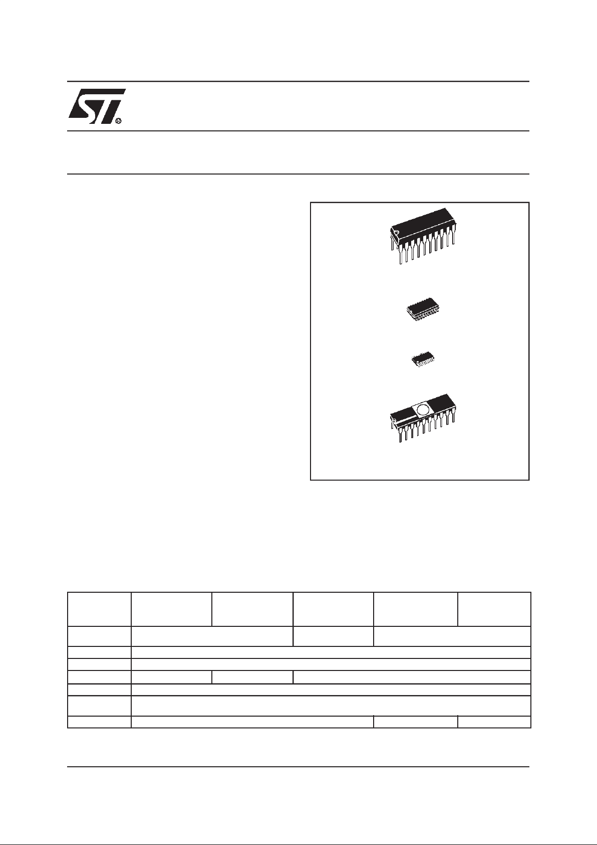
Device Summary
(See Section 12.5 for Ordering Information)
PDIP20
SO20
CDIP20W
SSOP20
Features
ST62T08C(OTP)/
ST6208C(ROM)
ST62P08C(FASTROM)
ST62T09C(OTP)/
ST6209C (ROM)
ST62P09C(FASTROM)
ST62T10C(OTP)/
ST6210C (ROM)
ST62P10C(FASTROM)
ST62T20C(OTP)
ST6220C(ROM)
ST62P20C(FASTROM)
ST62E20C(EPROM)
Program memory
- bytes
1K 2K 4K
RAM - bytes 64
Operating Supply 3.0V to 6V
Analog Inputs -
48
Clock Frequency 8MHz Max
Operating
Temperature
-40°C to +125°C
Packages PDIP20/SO20/SSOP20 PDIP20/SO20 CDIP20W
1
Page 2

Table of Contents
105
2/105
2
1 INTRODUCTION . . . . . . . . . . . . . . . . . . . . . .........................................6
2 PIN DESCRIPTION . . . . . . . . . . . . ................................................ 7
3 MEMORY MAPS, PROGRAMMING MODES AND OPTION BYTES . . . . . . . . . . . . . . . . . . . . . . 9
3.1 MEMORY AND REGISTER MAPS . ......................................... 9
3.1.1 Introduction . . . ..................................................... 9
3.1.2 Program Space . . . . . . . . . . . . . . . . . . . . ................................11
3.1.3 Readout Protection . . . . . . ...........................................11
3.1.4 Data Space . . . . . . . . . . . . . . . . . . . . . . . . ............................... 11
3.1.5 Stack Space . . . . . . . . . . . . ........................................... 11
3.1.6 Data ROM Window . . ............................................... 13
3.2 PROGRAMMING MODES . ............................................... 15
3.2.1 Program Memory . . . ................................................ 15
3.2.2 EPROM Erasing .................................................... 15
3.3 OPTION BYTES . . . .................................................... 16
4 CENTRAL PROCESSING UNIT . . ............................................... 17
4.1 INTRODUCTION . ...................................................... 17
4.2 MAIN FEATURES . . . . . . . . . . . . . . . . . . . . . . . . . . . . . . . . . . .................... 17
4.3 CPU REGISTERS . . . . . . . . . . . . . . . . . . . . . ................................. 17
5 CLOCKS, SUPPLY AND RESET . . . . . . . . . . . . . . . . . . . . . . . . . . . . . . . . . . . . . . . . . . . . . . . . 19
5.1 CLOCK SYSTEM . ...................................................... 19
5.1.1 Main Oscillator . .. . . . . . . . . . . . . . . . . . ................................. 20
5.1.2 Oscillator Safeguard (OSG) . . . ........................................ 21
5.1.3 Low Frequency Auxiliary Oscillator (LFAO) . . . . . . . . . . . .. . . . . . . . . . . . . . . . . . . 22
5.1.4 Register Description . . . . . . ........................................... 22
5.2 LOW VOLTAGE DETECTOR (LVD) . . . . . . . . ................................23
5.3 RESET . . . . . . . . . . . . . . . . . . . . . . . ........................................ 24
5.3.1 Introduction . . . .................................................... 24
5.3.2 RESET sequence . . . ............................................... 24
5.3.3 RESET Pin . . . . . . . . . ............................................... 25
5.3.4 Watchdog Reset . . . . . . . . . . . . . . . . . . ................................. 26
5.3.5 LVD Reset . . . . . . . . . ...............................................26
6 INTERRUPTS . . ............................................................. 27
6.1 INTERRUPT RULES AND PRIORITY MANAGEMENT . . . . . . . . . . . . . . . . . . . . . . . . . 28
6.2 INTERRUPTS AND LOW POWER MODES . . . . . . . . . . . . . . . . . . . . . . . . . . . . . . . . . . 28
6.3 NON MASKABLE INTERRUPT . . . . . . . . . . ..................................28
6.4 PERIPHERAL INTERRUPTS . . ........................................... 28
6.5 EXTERNAL INTERRUPTS (I/O PORTS) . . . .................................29
6.5.1 Notes on using External Interrupts .. . . . . . . .............................. 29
6.6 INTERRUPT HANDLING PROCEDURE . . . . . . . . . . . . . . . . . . . . . . . . . . . . . ........ 30
6.6.1 Interrupt Response Time . . . . . . . . . . . .................................. 30
6.7 REGISTER DESCRIPTION . . . . . . . . . . . . . . . . . . . . . . . . . . . . . . . . . . . . . . . ........ 31
Page 3

Table of Contents
3/105
3
7 POWER SAVING MODES . . . . . . . . . . ...........................................32
7.1 INTRODUCTION . ...................................................... 32
7.2 WAIT MODE . . . . . . . . . . . ............................................... 33
7.3 STOP MODE . . . . . . .................................................... 34
7.4 NOTES RELATED TO WAIT AND STOP MODES .............................36
7.4.1 Exit from Wait and Stop Modes . . . . ....................................36
7.4.2 Recommended MCU Configuration . . . . . . . . . . . . . . . . . . . . . . . . . . . . . ........ 36
8 I/O PORTS . . . . . . . . . . . . . . . . . . . . . . . . . . ........................................ 37
8.1 INTRODUCTION . ...................................................... 37
8.2 FUNCTIONAL DESCRIPTION . . . . ........................................37
8.2.1 Digital input modes . . . . . . ........................................... 37
8.2.2 Analog inputs . . . . . . . ...............................................37
8.2.3 Output modes . . . . . . ............................................... 37
8.2.4 Alternate functions . . . ...............................................37
8.2.5 Instructions NOT to be used to access Port Data registers (SET, RES, INC and DEC) 39
8.2.6 Recommendations . . . . . . . ...........................................39
8.3 LOW POWER MODES . . . . . . . . . . ........................................39
8.4 INTERRUPTS . . . . . . . . . . . . . . . . . . . . . . . . ................................. 39
8.5 REGISTER DESCRIPTION . . . . . . . . . . . . . . . . . . . . . . . . . . . . . . . . . . . . . . . ........ 41
9 ON-CHIP PERIPHERALS . . . . . . . . . . . ........................................... 42
9.1 WATCHDOG TIMER (WDG) . . . . . . . . . . . . . . . . . . . ........................... 42
9.1.1 Introduction . . . .................................................... 42
9.1.2 Main Features . . . . . . ...............................................42
9.1.3 Functional Description . . . . ...........................................43
9.1.4 Recommendations . . . . . . . ...........................................43
9.1.5 Low Power Modes . . . ............................................... 44
9.1.6 Interrupts . . . . . . . . . . . . . . . . . . . . . . . . ................................. 44
9.1.7 Register Description . . . . . . ........................................... 45
9.2 8-BIT TIMER . . . . ...................................................... 46
9.2.1 Introduction . . . .................................................... 46
9.2.2 Main Features . . . . . . ...............................................46
9.2.3 Counter/Prescaler Description . . . . . . . . . . . . . . . . . . . . . . . . . . . . . . . . . ........ 47
9.2.4 Functional Description . . . . ...........................................48
9.2.5 Low Power Modes . . . ............................................... 50
9.2.6 Interrupts . . . . . .................................................... 50
9.2.7 Register Description . . . . . . ........................................... 51
9.3 A/D CONVERTER (ADC) . . . . . . . . . . . . . . . . . . . . . ........................... 52
9.3.1 Introduction . . . .................................................... 52
9.3.2 Main Features . . . . . . ...............................................52
9.3.3 Functional description . . . . . . . . . . . . . . . . . . . . ........................... 53
9.3.4 Recommendations . . . . . . . ...........................................54
9.3.5 Low power modes . . . . . . . . . . . . . . . . . . ................................55
9.3.6 Interrupts . . . . . . . . . . . . . . . . . . . . . . . . ................................. 55
9.3.7 Register description . . . . . . ...........................................55
Page 4

Table of Contents
105
4/105
10 INSTRUCTION SET . . . . . . . . . . . . . . . . . . . . . . . . ................................. 56
10.1 ST6 ARCHITECTURE . . . . . . . . . . . . . . . . . .................................. 56
10.2 ADDRESSING MODES . . . . . . . . . . . . . . . . . . ................................56
10.3 INSTRUCTION SET . . . . . . . . . . . . . . . . . . . ................................. 57
11 ELECTRICAL CHARACTERISTICS . . . . ......................................... 62
11.1 PARAMETER CONDITIONS . . . . . . . . . . . . . . . . .............................. 62
11.1.1Minimum and Maximum values ........................................62
11.1.2Typical values . . . . . . . . . . ...........................................62
11.1.3Typical curves . . . . . . . . . . . . . ........................................ 62
11.1.4Loading capacitor . . . . . . . . . . . . . . . . . .................................. 62
11.1.5Pin input voltage . . . . . . . . . . . . . . . . . . . . . . . . . . . . . . . . . . . . . . . . . . . . . . . . . . . 62
11.2 ABSOLUTE MAXIMUM RATINGS . . . . . . . . . . . . . . . . . . . . . . . . . . . . . . . . . . . . . . . . . 63
11.2.1Voltage Characteristics . . . . . . . . . . . . . . . . . . . . . . . . . . . . . . . . . . . . . . . . . . . . . . 63
11.2.2Current Characteristics . . . . . . . . . . . . . . . . .............................. 63
11.2.3Thermal Characteristics . . . . . . . . . .................................... 63
11.3 OPERATING CONDITIONS . . . . . . . . . . .................................... 64
11.3.1General Operating Conditions . . . . .................................... 64
11.3.2Operating Conditions with Low Voltage Detector (LVD) . .................... 65
11.4 SUPPLY CURRENT CHARACTERISTICS . . . ................................66
11.4.1RUN Modes . . . . . . . . . . . . . . . . . . . . . . . . . . . . . . . . . . .................... 66
11.4.2WAIT Modes . . . . . . . . . . . ...........................................67
11.4.3STOP Mode . . . ................................................... 70
11.4.4Supply and Clock System . . . . . . . . . . . . . . . . . . . . . . .. . . . . . . . . . . . . . . . . . . . . 71
11.4.5On-Chip Peripherals . . . . . ...........................................71
11.5 CLOCK AND TIMING CHARACTERISTICS . . . . . . . . . . . . . . . . . . . . . . . ...........72
11.5.1General Timings . . . . . . . . . . . . . . . . . . . . . . . . . . . . . . . . . . . . . . . . . . . . . . . . . . . 72
11.5.2External Clock Source . . . . . . . . . . . ....................................72
11.5.3Crystal and Ceramic Resonator Oscillators . . . . ........................... 73
11.5.4RC Oscillator . . .................................................... 74
11.5.5Oscillator Safeguard (OSG) and Low Frequency Auxiliary Oscillator (LFAO) . . . . . 75
11.6 MEMORY CHARACTERISTICS . . . ........................................76
11.6.1RAM and Hardware Registers . . . . . . . . . . . . . . . . . . . . . . . . . ............... 76
11.6.2EPROM Program Memory . . . . . . . . . . ................................. 76
11.7 EMC CHARACTERISTICS . . . . . . . . . . . . . . . . . . . . . . . . . . . . . . . . . . . . . . . . . . . . . . . 77
11.7.1Functional EMS . . . . . ............................................... 77
11.7.2Absolute Electrical Sensitivity . . . . . . . . . . . . . . ........................... 78
11.7.3ESD Pin Protection Strategy . . . . . . . . . . . . . . . . . . . . . . . . . . . . . . . . . . . . . . . . . . 80
11.8 I/O PORT PIN CHARACTERISTICS ........................................81
11.8.1General Characteristics . . . . . . . . . . . . ..................................81
11.8.2Output Driving Current . . . . ........................................... 82
11.9 CONTROL PIN CHARACTERISTICS . . . . . .................................. 85
11.9.1Asynchronous RESET Pin . . . . . . . . . . . . . . . . . ........................... 85
11.9.2NMI Pin . . . . . . . . . . . . . . . ...........................................86
1
Page 5

Table of Contents
5/105
11.10 TIMER PERIPHERAL CHARACTERISTICS . . . . . . . . . . . . . . . . . . . . . . . . . . ........87
11.10.1Watchdog Timer .. . . . . . . . . . . . . . . . . . . . . . . . . . . . . . . . . . . . . . . . . ........ 87
11.10.28-Bit Timer . . . . . . . . . . . . ...........................................87
11.11 8-BIT ADC CHARACTERISTICS .. . . . . . . .................................. 88
12 GENERAL INFORMATION .................................................... 90
12.1 PACKAGE MECHANICAL DATA . . . . . . . . . . . . .............................. 90
12.2 THERMAL CHARACTERISTICS . . . . . . . . . . . . . . . . . . . . . . .................... 92
12.3 SOLDERING AND GLUEABILITY INFORMATION . . . . . . . . . . . . . . . . . . . . . ........93
12.4 PACKAGE/SOCKET FOOTPRINT PROPOSAL . . . . . . . . . . . .................... 94
12.5 ORDERING INFORMATION . . . . . . . . .. . . . . . . .............................. 95
12.6 TRANSFER OF CUSTOMER CODE .. . . . . . . . . . . . . . . . . . . . . . . . . . . . . . ........96
12.6.1FASTROM version . . . ............................................... 96
12.6.2ROM VERSION .................................................... 98
13 DEVELOPMENT TOOLS . . . . . . . . . . .......................................... 100
14 ST6 APPLICATION NOTES . . . . . . . . . . . . . . . . . . . . . ............................. 102
15 SUMMARY OF CHANGES . .................................................. 104
16 TO GET MORE INFORMATION . .............................................. 104
1
Page 6
ST6208C/ST6209C/ST6210C/ST6220C
6/105
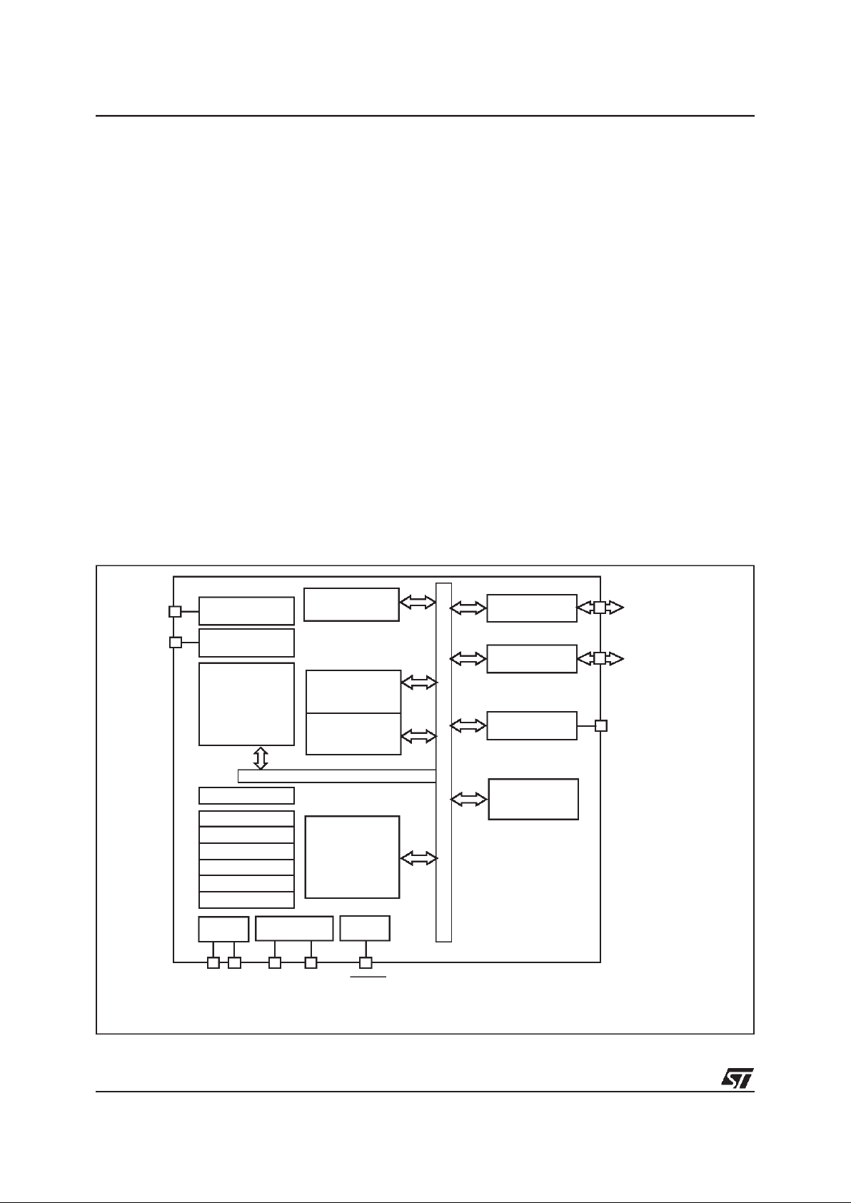
1 INTRODUCTION
The ST6208C, 09C, 10C and 20Cdevices are low
cost members of the ST62xx 8-bit HCMOS family
of microcontrollers, which is targeted at low to medium complexity applications. All ST62xx devices
are based on a building block approach: a common core is surrounded by a number of on-chip
peripherals.
The ST62E20C isthe erasable EPROM versionof
the ST62T08C, T09C, T10C and T20C devices,
which may be usedduring the development phase
for the ST62T08C, T09C, T10C and T20C target
devices, as well as the respective ST6208C, 09C,
10C and 20C ROM devices.
OTP and EPROM devices are functionally identical. OTP devices offer all the advantages of user
programmability at low cost, which make them the
ideal choice in a wide range of applications where
frequent code changes, multiple code versions or
last minute programmability are required.
The ROM based versions offer the same functionality, selecting the options defined in the program-
mable option bytes of the OTP/EPROM versions
in the ROM option list (See Section 12.6 on page
96).
The ST62P08C/P09C/P10C/P20C are the Factory
Advanced Service Technique ROM (FASTROM)
versions of ST62T08C, T09C, T10C and T20C
OTP devices.
They offer the same functionality as OTP devices,
but they do not have to be programmed by the
customer (See Section 12 on page 90).
These compact low-cost devices feature a Timer
comprising an 8-bit counter with a 7-bit programmable prescaler, an 8-bit A/D Converter with up to
8 analog inputs (depending on device) and a Digital Watchdog timer, making them well suited for a
wide range of automotive, applianceand industrial
applications.
For easy reference, all parametric dataare located
in Section 11 on page 62.
Figure 1. Block Diagram
TEST
NMI INTERRUPTS
PROGRAM
PC
STACKLEVEL 1
STACKLEVEL 2
STACKLEVEL 3
STACKLEVEL 4
STACKLEVEL 5
STACKLEVEL 6
POWER
SUPPLY
OSCILLATOR
RESET
DATA ROM
USER
SELECTABLE
DATA RAM
64 Bytes
PORT A
PORT B
TIMER
8-BIT CORE
TEST/V
PP
8-BIT *
A/D CONVERTER
PA0..PA3 (20mA Sink)
PB0..PB7 / Ain*
TIMER
V
DDVSS
OSCin OSCout RESET
WATCHDOG
:
MEMORY
TIMER
(1K, 2K
* Depending on device. See device summary on page 1.
or 4K Bytes)
4
Page 7
ST6208C/ST6209C/ST6210C/ST6220C
7/105
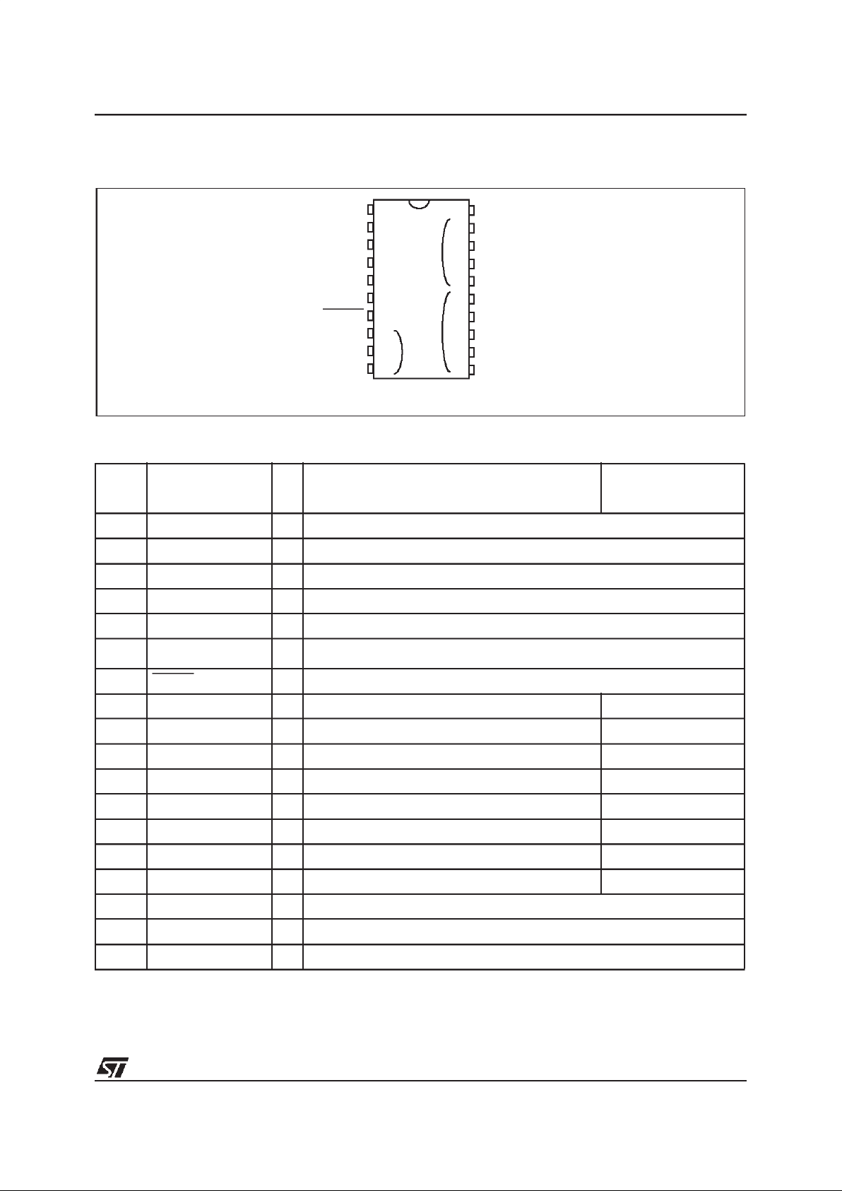
2 PIN DESCRIPTION
Figure 2. 20-Pin Package Pinout
Table 1. Device Pin Description
V
DD
TIMER
Ain*/PB5
Ain*/PB6
Ain*/PB7
RESET
V
PP
/TEST
NMI
OSCout
OSCin
V
SS
PA0/20mA Sink
PB4/Ain*
PB3/Ain*
PB2/Ain*
PB1/Ain*
PB0/Ain*
PA3/20mA Sink
PA2/20mA Sink
PA1/20mA Sink
itX associated interrupt vector
1
2
3
4
5
6
7
8
9
10
11
12
20
19
18
17
16
15
14
13
* Depending on device. See device summary on page 1
it2
it1
it2
Pin n° Pin Name
Type
Main Function
(after Reset)
Alternate Function
1V
DD
S Main power supply
2
TIMER I/O Timer input or output
3 OSCin I External clock input or resonator oscillator inverter input
4 OSCout O Resonator oscillator inverter output or resistor input for RC oscillator
5 NMI I Non maskable interrupt (falling edge sensitive)
6V
PP
/TEST
Must be held at Vss for normal operation, if a 12.5V level is applied to the pin
during the reset phase, the device enters EPROM programming mode.
7 RESET I/O Top priority non maskable interrupt (active low)
8 PB7/Ain* I/O Pin B7 (IPU) Analog input
9 PB6/Ain* I/O Pin B6 (IPU) Analog input
10 PB5/Ain* I/O Pin B5 (IPU) Analog input
11 PB4/Ain* I/O Pin B4 (IPU) Analog input
12 PB3/Ain* I/O Pin B3 (IPU) Analog input
13 PB2/Ain* I/O Pin B2 (IPU) Analog input
14 PB1/Ain* I/O Pin B1 (IPU) Analog input
15 PB0/Ain* I/O Pin B0 (IPU) Analog input
16 PA3/ 20mA Sink I/O Pin A3 (IPU)
17 PA2/ 20mA Sink I/O Pin A2 (IPU)
18 PA1/ 20mA Sink I/O Pin A1 (IPU)
5
Page 8

ST6208C/ST6209C/ST6210C/ST6220C
8/105
Legend / Abbreviations for Table 1:
* Depending on device. See device summary on page 1.
I = input, O = output, S = supply, IPU = input with pull-up
The input with pull-up configuration (reset state) is valid as long as the user software does not change it.
Refer to Section 8 ”I/O PORTS” onpage 37 for more detailson the software configuration of the I/O ports.
19 PA0/ 20mA Sink I/O Pin A0 (IPU)
20 V
SS
S Ground
Pin n° Pin Name
Type
Main Function
(after Reset)
Alternate Function
6
Page 9
ST6208C/ST6209C/ST6210C/ST6220C
9/105
3 MEMORY MAPS, PROGRAMMING MODES AND OPTION BYTES
3.1 MEMORY AND REGISTER MAPS
3.1.1 Introduction
The MCU operates in three separate memory
spaces: Program space, Data space, and Stack
space. Operation in thesethree memory spaces is
described in the following paragraphs.
Briefly, Program space contains user program
code in OTP and user vectors; Data space contains user data in RAM and in OTP, and Stack
space accommodates six levels of stack for subroutine and interrupt service routine nesting.
Figure 3. Memory Addressing Diagram
PROGRAM SPACE
PROGRAM
INTERRUPT &
RESET VECTORS
ACCUMULATOR
RAM
X REGISTER
Y REGISTER
V REGISTER
W REGISTER
000h
03Fh
040h
07Fh
080h
081h
082h
083h
084h
0C0h
0FFh
DATA SPACE
000h
0FF0h
0FFFh
MEMORY
WINDOW
DATA ROM
RESERVED
HARDWARE
CONTROL
REGISTERS
0BFh
(see Table 2)
(see Figure 4)
1
Page 10
ST6208C/ST6209C/ST6210C/ST6220C
10/105
MEMORY MAP (Cont’d)
Figure 4. Program Memory Map
(*) Reserved areas should be filled with 0FFh
0000h
0AFFh
0B00h
0B9Fh
NOT IMPLEMENTED
RESERVED
*
USER
PROGRAM MEMORY
1024 BYTES
0BA0h
0F9Fh
0FA0h
0FEFh
0FF0h
0FF7h
0FF8h
0FFBh
0FFCh
0FFDh
0FFEh
0FFFh
RESERVED
*
RESERVED
*
INTERRUPT VECTORS
NMI VECTOR
USER RESET VECTOR
0000h
07Fh
USER
PROGRAM MEMORY
3872 BYTES
080h
0F9Fh
0FA0h
0FEFh
0FF0h
0FF7h
0FF8h
0FFBh
0FFCh
0FFDh
0FFEh
0FFFh
RESERVED
*
RESERVED
*
INTERRUPT VECTORS
NMI VECTOR
USER RESET VECTOR
RESERVED
*
0000h
07FFh
0800h
087Fh
NOT IMPLEMENTED
RESERVED
*
USER
PROGRAM MEMORY
1824 BYTES
0880h
0F9Fh
0FA0h
0FEFh
0FF0h
0FF7h
0FF8h
0FFBh
0FFCh
0FFDh
0FFEh
0FFFh
RESERVED
*
RESERVED
*
INTERRUPT VECTORS
NMI VECTOR
USER RESET VECTOR
ST6208C, 09C ST6210C ST6220C
1
Page 11

ST6208C/ST6209C/ST6210C/ST6220C
11/105
MEMORY MAP (Cont’d)
3.1.2 Program Space
Program Space comprises the instructions to be
executed, the data required for immediate addressing mode instructions, the reserved factory
test area and the user vectors. Program Space is
addressed via the 12-bit ProgramCounter register
(PC register). Thus, the MCU is capable of addressing 4K bytes of memory directly.
3.1.3 Readout Protection
The Program Memory in OTP, EPROM or ROM
devices can be protected against external readout
of memory by setting the Readout Protectionbit in
the option bytes (Section 3.3 on page 16).
In the EPROM parts, Readout Protection option
can be desactivated only by U.V. erasure that also
results in the whole EPROM context being erased.
Note: Once the Readout Protection is activated, it
is no longer possible, even for STMicroelectronics,
to gain access to the OTP or ROM contents. Returned parts can therefore not be accepted if the
Readout Protection bit is set.
3.1.4 Data Space
Data Space accommodates all the data necessary
for processing the user program. This space comprises the RAM resource, the processor core and
peripheral registers, as well as read-only data
such as constants and look-up tables in OTP/
EPROM.
3.1.4.1 Data ROM
All read-only data is physically stored in program
memory, which also accommodates the Program
Space. The program memory consequently contains the program code to be executed, as well as
the constants and look-up tables required by the
application.
The Data Space locations in which the different
constants and look-up tables are addressed bythe
processor core may be thought of as a 64-byte
window through which it is possible to access the
read-only data stored in OTP/EPROM.
3.1.4.2 Data RAM
The data space includes the user RAM area, the
accumulator (A), the indirect registers (X), (Y), the
short direct registers (V), (W), the I/O port registers, the peripheral data and control registers, the
interrupt option register and the Data ROM Window register (DRWR register).
3.1.5 Stack Space
Stack space consists of six 12-bit registers which
are used to stack subroutine and interrupt return
addresses, as well as the current program counter
contents.
1
Page 12
ST6208C/ST6209C/ST6210C/ST6220C
12/105
MEMORY MAP (Cont’d)
Table 2. Hardware Register Map
Legend:
x = undefined, R/W = Read/Write, Ro = Read-only Bit(s) in the register, Wo = Write-only Bit(s)
in the register.
Notes:
1. The contents of the I/O port DR registers are readable only in output configuration. In input configuration, the values of the I/O pins are returned instead of the DR register contents.
2. The bits associated with unavailable pins mustalways be kept at their reset value.
3. Do notuse single-bit instructions (SET, RES...) on Port Data Registersif anypin ofthe port is configured
in input mode (refer to Section 8 ”I/O PORTS” on page 37 for more details)
4. Depending on device. See device summary on page 1.
Address Block
Register
Label
Register Name
Reset
Status
Remarks
080h
to 083h
CPU X,Y,V,W
X,Y index registers
V,W short direct registers
xxh R/W
0C0h
0C1h
I/O Ports
DRA
1) 2) 3)
DRB
1) 2) 3)
Port A Data Register
Port B Data Register
00h
00h
R/W
R/W
0C2h
0C3h
Reserved (2 Bytes)
0C4h
0C5h
I/O Ports
DDRA
2)
DDRB
2)
Port A Direction Register
Port B Direction Register
00h
00h
R/W
R/W
0C6h
0C7h
Reserved (2 Bytes)
0C8h IOR Interrupt Option Register xxh Write-only
0C9h DRWR Data ROM Window register xxh Write-only
0CAh
0CBh
Reserved (2 Bytes)
0CCh
0CDh
I/O Ports
ORA
2)
ORB
2)
Port A Option Register
Port B Option Register
00h
00h
R/W
R/W
0CEh
0CFh
Reserved (2 bytes)
0D0h
0D1h
ADC
4)
ADR
ADCR
A/D Converter Data Register
A/D Converter Control Register
xxh
40h
Read-only
Ro/Wo
0D2h
0D3h
0D4h
Timer1
PSCR
TCR
TSCR
Timer 1 Prescaler Register
Timer 1 Downcounter Register
Timer 1 Status Control Register
7Fh
0FFh
00h
R/W
R/W
R/W
0D5h
to 0D7h
Reserved (3 Bytes)
0D8h
Watchdog
Timer
WDGR Watchdog Register 0FEh R/W
0D9h
to 0FEh
Reserved (38 Bytes)
0FF CPU A Accumulator xxh R/W
1
Page 13
ST6208C/ST6209C/ST6210C/ST6220C
13/105
MEMORY MAP (Cont’d)
3.1.6 Data ROM Window
The Data read-only memory window is located
from address 0040h to address 007Fh in Data
space. It allows direct reading of 64 consecutive
bytes located anywhere in program memory, between address 0000h and 0FFFh.
There are 64 blocks of 64 bytes in a 4K device:
– Block 0is related to the address range 0000h to
003Fh.
– Block 1is related to the address range 0040h to
007Fh.
and so on...
All the program memory can therefore be used to
store either instructions or read-only data. The
Data ROM window can be moved in steps of 64
bytes along the program memory by writing the
appropriate code inthe Data ROM WindowRegister (DRWR).
Figure 5. Data ROM Window
3.1.6.1 Data ROM Window Register (DRWR)
The DRWR can be addressed like any RAM location in the Data Space.
This register is used to select the 64-byte block of
program memory to be read in the Data ROM window (from address 40h to address 7Fh in Data
space). The DRWR register is not cleared on reset, therefore it must be written to before accessing the Data read-only memory window area for
the first time.
Address: 0C9h — Write Only
Reset Value = xxh (undefined)
Bits 6, 7 = Not used.
Bit 5:0 = DRWR[5:0]
Data read-only memory Win-
dow Register Bits.
These are the Data read-only
memory Window bits that correspondto the upper
bits of the data read-only memory space.
Caution:
This register is undefined on reset, it is
write-only, thereforedo notread it nor access it using single-bit instructions (SET, RES...).
0000h
0FFFh
000h
040h
07Fh
0FFh
DATA ROM
WINDOW
DATA SPACE
64-BYTE
ROM
PROGRAM
SPACE
70
- - DRWR5 DRWR4 DRWR3 DRWR2 DRWR1 DRWR0
1
Page 14
ST6208C/ST6209C/ST6210C/ST6220C
14/105
MEMORY MAP (Cont’d)
3.1.6.2 Data ROM Window memory addressing
In cases where some data (look-up tables for example) are stored in program memory, reading
these data requires the use of the Data ROM window mechanism. To do this:
1. The DRWR register has to be loaded with the
64-byte block number where the data are located
(in program memory). This number also gives the
start address of the block.
2. Then, the offset address of the byte in the Data
ROM Window (corresponding to the offset in the
64-byte block in programmemory) has to be loaded in a register (A, X,...).
When the above two steps are completed, the
data can be read.
To understand how to determine the DRWR and
the content of the register, please refer to the example shown in Figure 6. In any case the calcula-
tion is automatically handled by the ST6 development tools.
Please refer to the user manual of the correspoding tool.
3.1.6.3 Recommendations
Care is required when handling the DRWR register as it is write only. For this reason, the DRWR
contents should not be changed while executing
an interrupt service routine, as the service routine
cannot save and then restore the register’s previous contents. If it is impossible to avoid writing to
the DRWR during the interrupt service routine, an
image of the register must be saved in a RAM location, and each time the program writes to the
DRWR, it must also write to the image register.
The image register must be written first so that, if
an interrupt occurs between the two instructions,
the DRWR is not affected.
Figure 6. Data ROM Window Memory Addressing
DATA
PROGRAM SPACE
DATA SPACE
0000h
0400h
0421h
07FFh
64 bytes
OFFSET
000h
040h
061h
07Fh
OFFSET
21h
0FFh
DRWR
DATA address in Program memory : 421h
DRWR content : 421h / 3Fh (64) = 10H data is located in 64-bytes window number 10h
64-byte window start address : 10h x 3Fh = 400h
Register (A, X,...)content : Offset = (421h - 400h) + 40h ( Data ROM Window start address in data space) = 61h
10h
DATA
1
Page 15

ST6208C/ST6209C/ST6210C/ST6220C
15/105
3.2 PROGRAMMING MODES
3.2.1 Program Memory
EPROM/OTP programming mode is set by a
+12.5V voltage applied to the TEST/VPPpin. The
programming flow of the ST62T08C,T09C,T10C,
T20C and E20C isdescribed in the User Manual of
the EPROM Programming Board.
Table 3. ST6208C/09C Program Memory Map
Table 4. ST6210C Program Memory Map
Table 5. ST6220C Program Memory Map
Note: OTP/EPROM devices can be programmed
with the development tools available from
STMicroelectronics (please refer to Section 13 on
page 100).
3.2.2 EPROM Erasing
The EPROM devices can be erased by exposure
to Ultra Violet light. The characteristics of the MCU
are such that erasure begins when the memory is
exposed to light with a wave lengths shorter than
approximately 4000Å. It should be noted that sunlight and some types of fluorescent lamps have
wavelengths in the range 3000-4000Å.
It is thus recommended that the window of the
MCU packages be covered by an opaque label to
prevent unintentional erasure problems when testing the application in such an environment.
The recommended erasure procedure is exposure
to short wave ultraviolet light which have a wavelength 2537Å. The integrated dose (i.e. U.V. intensity x exposure time) for erasure should be a minimum of 30W-sec/cm2. The erasure time with this
dosage is approximately30 to 40 minutes using an
ultraviolet lamp with 12000µW/cm2power rating.
The EPROM device should be placed within
2.5cm (1inch) of the lamp tubes during erasure.
Device Address Description
0000h-0B9Fh
0BA0h-0F9Fh
0FA0h-0FEFh
0FF0h-0FF7h
0FF8h-0FFBh
0FFCh-0FFDh
0FFEh-0FFFh
Reserved
User ROM
Reserved
Interrupt Vectors
Reserved
NMI Interrupt Vector
Reset Vector
Device Address Description
0000h-087Fh
0880h-0F9Fh
0FA0h-0FEFh
0FF0h-0FF7h
0FF8h-0FFBh
0FFCh-0FFDh
0FFEh-0FFFh
Reserved
User ROM
Reserved
Interrupt Vectors
Reserved
NMI Interrupt Vector
Reset Vector
Device Address Description
0000h-007Fh
0080h-0F9Fh
0FA0h-0FEFh
0FF0h-0FF7h
0FF8h-0FFBh
0FFCh-0FFDh
0FFEh-0FFFh
Reserved
User ROM
Reserved
Interrupt Vectors
Reserved
NMI Interrupt Vector
Reset Vector
1
Page 16

ST6208C/ST6209C/ST6210C/ST6220C
16/105
3.3 OPTION BYTES
Each deviceis available for production in user programmable versions (OTP) as well as in factory
coded versions (ROM). OTP devices are shipped
to customers with a default content (00h), while
ROM factory coded parts contain the code supplied by the customer. This implies that OTP devices have to be configured by the customer using
the OptionBytes while the ROM devices are factory-configured.
The two option bytes allow the hardware configuration of the microcontroller to be selected.
The option bytes have no address in the memory
map and can be accessed only in programming
mode (for example using a standard ST6 programming tool).
In masked ROM devices, the option bytes are
fixed in hardware by the ROM code (see Section
12.6.2 ”ROM VERSION” on page 98).
The option bytes can be only programmed once. It
is not possible tochange theselected optionsafter
they have been programmed.
MSB OPTION BYTE
Bit 15:10 = Reserved, must be always cleared.
Bit 9 = EXTCNTL
External STOP MODE control.
0: EXTCNTL mode not available. STOP mode is
not available with the watchdog active.
1: EXTCNTL mode available. STOP mode is avail-
able with the watchdogactive by setting NMIpin
to one.
Bit 8 = LVD
Low Voltage Detector
on/off
.
This option bit enable or disable the Low Voltage
Detector (LVD) feature.
0: Low Voltage Detector disabled
1: Low Voltage Detector enabled
LSB OPTION BYTE
Bit 7 = PROTECT
Readout Protection.
This option bit enables or disables external access
to the internal program memory.
0: Program memory not read-out protected
1: Program memory read-out protected
Bit 6 = OSC
Oscillator selection
.
This option bit selects the main oscillator type.
0: Quartz crystal, ceramic resonator or external
clock
1: RC network
Bit 5 = Reserved, must be always cleared.
Bit 4 = Reserved, must be always set.
Bit 3 = NMI PULL
NMI Pull-Up
on/off.
This option bitenables or disables the internalpullup on the NMI pin.
0: Pull-up disabled
1: Pull-up enabled
Bit 2 = TIM PULL
TIMER Pull-Up
on/off.
This option bitenables or disables the internalpullup on the TIMER pin.
0: Pull-up disabled
1: Pull-up enabled
Bit 1 = WDACT
Hardware or software watchdog.
This option bit selects the watchdog type.
0: Software (watchdog to be enabled by software)
1: Hardware (watchdog always enabled)
Bit 0 = OSGEN
Oscillator Safeguard
on/off.
This option bit enables or disables the oscillator
Safeguard (OSG) feature.
0: Oscillator Safeguard disabled
1: Oscillator Safeguard enabled
MSB OPTION BYTE
15 8
LSB OPTION BYTE
70
Reserved
EXT
CTL
LVD
PRO-
TECT
OSC Res. Res.
NMI
PULL
TIM
PULLWDACT
OSG
EN
Default
Value
XXXXXXXXXXXXX X X X
1
Page 17
ST6208C/ST6209C/ST6210C/ST6220C
17/105
4 CENTRAL PROCESSING UNIT
4.1 INTRODUCTION
The CPU Coreof ST6devicesisindependent ofthe
I/O or Memory configuration. As such, it may be
thought of as an independent central processor
communicating with on-chip I/O, Memory and Peripherals via internal address, data, and control
buses.
4.2 MAIN FEATURES
■ 40 basic instructions
■ 9 main addressing modes
■ Two 8-bit index registers
■ Two 8-bit short direct registers
■ Low power modes
■ Maskable hardware interrupts
■ 6-level hardware stack
4.3 CPU REGISTERS
TheST6FamilyCPUcorefeaturessixregisters and
three pairs of flags available to the programmer.
These are described in the following paragraphs.
Accumulator (A). The accumulator is an 8-bit
general purpose register used in all arithmetic calculations, logical operations, and data manipula-
tions. The accumulator can be addressed in Data
Space as a RAM location at address FFh. Thus
the ST6 can manipulate the accumulator just like
any other register in Data Space.
Index Registers (X, Y). These two registers are
used in Indirect addressing mode as pointers to
memory locations in Data Space. They can also
be accessed in Direct, Short Direct, or Bit Direct
addressing modes. They are mapped in Data
Space at addresses 80h (X) and 81h (Y) and can
be accessed like any other memory location.
Short Direct Registers (V, W). These two registers are used in Short Direct addressing mode.
This means that the data stored in V or W can be
accessed with aone-byte instruction (four CPU cycles). V and W can also be accessed using Direct
and Bit Direct addressing modes. They are
mapped in Data Space at addresses 82h (V) and
83h (W) and canbe accessed like any other memory location.
Note: The X and Y registers can also be used as
Short Directregisters inthe same way as V and W.
Program Counter (PC). Theprogram counter is a
12-bit register which contains the address of the
next instruction to be executed by the core. This
ROM location may be an opcode, an operand, or
the address of an operand.
Figure 7. CPU Registers
ACCUMULATOR
X INDEX REGISTER
Y INDEX REGISTER
PROGRAM COUNTER
RESET VALUE = RESET VECTOR @ 0FFEh-0FFFh
70
70
70
0
11
RESET VALUE = xxh
RESET VALUE = xxh
RESET VALUE = xxh
x = Undefined value
V SHORT INDIRECT
70
RESET VALUE = xxh
W SHORTINDIRECT
70
RESET VALUE = xxh
NORMAL FLAGS
CN ZN
CI ZI
CNMI ZNMI
INTERRUPT FLAGS
NMI FLAGS
SIX LEVEL
STACK
REGISTER
REGISTER
1
Page 18
ST6208C/ST6209C/ST6210C/ST6220C
18/105
CPU REGISTERS (Cont’d)
The 12-bit length allows the direct addressing of
4096 bytes in Program Space.
However, ifthe program space contains more than
4096 bytes, the additional memory in program
space can be addressed by using the Program
ROM Page register.
The PC value is incremented after reading the address of the current instruction.To execute relative
jumps, the PC and the offset are shifted through
the ALU, where they are added; the result is then
shifted back into the PC.The program counter can
be changedin the following ways:
– JP (Jump) instruction PC = Jump address
– CALL instruction PC = Call address
– Relative Branch InstructionPC = PC +/- offset
– Interrupt PC = Interrupt vector
– Reset PC = Reset vector
– RET & RETI instructions PC = Pop (stack)
– Normal instruction PC = PC + 1
Flags (C, Z). The ST6 CPU includes three pairs of
flags (Carry and Zero), each pair beingassociated
with one of the three normal modes of operation:
Normal mode, Interrupt mode and Non Maskable
Interrupt mode. Each pair consists of a CARRY
flag and a ZERO flag. One pair (CN, ZN) is used
during Normal operation, another pair is usedduring Interrupt mode (CI, ZI), and a third pair is used
in the Non Maskable Interrupt mode (CNMI, ZNMI).
The ST6 CPU uses the pair of flags associated
with the current mode: as soon as an interrupt (or
a Non Maskable Interrupt) is generated, the ST6
CPU uses the Interrupt flags (or the NMI flags) instead of the Normal flags. When the RETI instruction is executed, the previously used set of flags is
restored. It should be noted that each flag set can
only be addressed in its own context (Non Maskable Interrupt, Normal Interrupt or Main routine).
The flags are not cleared during context switching
and thus retain their status.
C : Carry flag.
This bit is set when acarry or aborrow occurs dur-
ing arithmetic operations; otherwise it is cleared.
The Carry flag is also set to the value of the bit
tested in a bit test instruction; it also participates in
the rotate left instruction.
0: No carry has occured
1: A carry has occured
Z : Zero flag
This flag is set if the result of the last arithmetic or
logical operation was equal to zero; otherwise it is
cleared.
0: The result of the last operation is different from
zero
1: The result of the last operation is zero
Switching between the three sets of flags is per-
formed automatically whenan NMI, an interrupt or
a RETI instruction occurs. As NMI mode is automatically selected after the reset of the MCU, the
ST6 core uses the NMI flags first.
Stack. The ST6 CPU includes a true LIFO (Last In
First Out) hardware stack which eliminates the
need for a stackpointer. The stack consists of six
separate 12-bit RAM locations that do not belong
to the data space RAM area. When a subroutine
call (or interrupt request) occurs, the contents of
each level are shifted into the next level down,
while the content of the PC is shifted into the first
level (the original contents of the sixth stack level
are lost). When a subroutine or interrupt return occurs (RET or RETI instructions), the first level register is shifted back into the PC and the value of
each level is popped back into the previous level.
Figure 8. Stack manipulation
Since the accumulator, in common with all other
data space registers, is not stored in this stack,
management of these registers should be performed within the subroutine.
Caution: The stack will remain in its“deepest” position if more than 6 nested calls or interrupts are
executed, and consequently the last return address will be lost.
It will also remain in its highest position if the stack
is empty and a RET or RETI is executed. In this
case the next instruction will be executed.
LEVEL 1
LEVEL 2
LEVEL 3
LEVEL 4
LEVEL 5
LEVEL 6
ON
INTERRUPT,
OR
SUBROUTINE
CALL
ON RETURN
FROM
INTERRUPT,
OR
SUBROUTINE
PROGRAM
COUNTER
1
Page 19
ST6208C/ST6209C/ST6210C/ST6220C
19/105
5 CLOCKS, SUPPLY AND RESET
5.1 CLOCK SYSTEM
The main oscillator of the MCU can be driven by
any of these clock sources:
– external clock signal
– external AT-cut parallel-resonant crystal
– external ceramic resonator
– external RC network (R
NET
).
In addition, an on-chip Low Frequency Auxiliary
Oscillator (LFAO) is available as a back-up clock
system or to reduce power consumption.
An optional Oscillator Safeguard (OSG) filters
spikes from the oscillator lines, and switches to the
LFAO backup oscillator in the event of main oscillator failure. It also automatically limits the internal
clock frequency(f
INT
) as a function of VDD, in order
to guarantee correct operation. These functions
are illustrated in Figure 10, and Figure 11.
Table 6 illustrates various possible oscillator configurations using an external crystal or ceramic
resonator, an external clock input, an external resistor (R
NET
), or the lowestcost solution using only
the LFAO.
For more details on configuring the clock options,
refer to the Option Bytes section of this document.
The internal MCU clock frequency (f
INT
) is divided
by 12 to drive the Timer, the Watchdog timer and
the A/D converter (if available), and by 13 to drive
the CPU core, as shown in Figure 9.
With an 8 MHz oscillator, the fastest CPU cycle is
therefore 1.625µs.
A CPU cycle is the smallest unit of time needed to
execute any operation (for instance, to increment
the Program Counter). An instruction may require
two, four, or five CPU cycles for execution.
Figure 9. Clock Circuit Block Diagram
MAIN
OSCILLATOR
OSG
LFAO
CORE
:13
:12
8-BIT TIMER
WATCHDOG
f
INT
OSCOFF BIT
ADC
0
1
filtering
OSCILLATOR SAFEGUARD (OSG)
OSG ENABLEOPTION BIT (See OPTION BYTE SECTION)
(ADCR REGISTER)
f
OSC
* Depending on device. See device summary on page 1.
*
*
1
Page 20
ST6208C/ST6209C/ST6210C/ST6220C
20/105
CLOCK SYSTEM (Cont’d)
5.1.1 Main Oscillator
The oscillator configuration is specified by selecting the appropriate option in the option bytes (refer
to the Option Bytes section of this document).
When the CRYSTAL/RESONATOR option is selected, it must be used with a quartz crystal, a ceramic resonator or an external signal provided on
the OSCin pin. When theRC NETWORK option is
selected, the system clock is generated by an external resistor (the capacitor is implemented internally).
The main oscillator can be turned off (when the
OSG ENABLED option is selected) by setting the
OSCOFF bit of the ADC Control Register (not
available onsome devices). This will automatically
start the Low Frequency Auxiliary Oscillator
(LFAO).
The main oscillator can be turned off by resetting
the OSCOFFbit of the A/D Converter Control Register or by resetting the MCU. When the main oscillator starts there is a delay made up of the oscillator start-up delay period plus the duration of the
software instruction at a clock frequency f
LFAO
.
Caution: It should be noted that when the RC network option is selected, the accuracy of the frequency is about 20% so it may not be suitable for
some applications (For more details, please refer
to the Electrical Characteristics Section).
Table 6. Oscillator Configurations
Notes:
1. To select the options shown in column 1 of the above
table, refer to the Option Byte section.
2.This schematic are given for guidance only and are subject to the schematics given by the crystal or ceramic resonator manufacturer.
3. For more details, please refer to the Electrical Characteristics Section.
Hardware Configuration
Crystal/Resonator Option
1)
Crystal/Resonator Option
1)
RC Network Option
1)
OSG Enabled Option
1)
OSCin OSCout
EXTERNAL
ST6
CLOCK
NC
External Clock
OSCin OSCout
LOAD
CAPACITORS
3)
ST6
C
L2
C
L1
Crystal/Resonator Clock
2)
OSCin OSCout
ST6
R
NET
NC
RC Network
OSCin OSCout
ST6
LFAO
NC
1
Page 21
ST6208C/ST6209C/ST6210C/ST6220C
21/105
CLOCK SYSTEM (Cont’d)
5.1.2 Oscillator Safeguard (OSG)
The Oscillator Safeguard (OSG) feature is a
means of dramatically improving the operational
integrity of the MCU. It is available when the OSG
ENABLED option is selected in the option byte (refer to the Option Bytes section of this document).
The OSG acts as a filter whose cross-over frequency is device dependent and provides three
basic functions:
– Filtering spikes on the oscillator lines which
would result in driving the CPU at excessive frequencies
– Management of the Low Frequency Auxiliary
Oscillator (LFAO), (useable as low cost internal
clock source, backup clockin case of main oscillator failure or for low power consumption)
– Automaticallylimiting thef
INT
clockfrequency as
a function of supply voltage, to ensure correct
operation even if the power supply drops.
5.1.2.1 Spike Filtering
Spikes onthe oscillator lines result in an effectively
increased internal clock frequency. In the absence
of an OSG circuit, this may lead to an over frequency for a given power supply voltage. The
OSG filters out such spikes (asillustrated inFigure
10). In all cases, when theOSG isactive, the max-
imum internal clock frequency, f
INT
, is limited to
f
OSG
, which is supply voltage dependent.
5.1.2.2 Management of Supply Voltage
Variations
Over-frequency, at a given power supply level, is
seen by the OSG as spikes; it therefore filters out
some cycles in order that the internal clock frequency of the device is kept within the range the
particular device can stand (depending on VDD),
and below f
OSG
: the maximum authorised frequen-
cy with OSG enabled.
5.1.2.3 LFAO Management
When the OSG is enabled, the Low Frequency
Auxiliary Oscillator can be used (see Section
5.1.3).
Note:The OSG should be used wherever possible
as it provides maximum security for the application. It should be noted however, that it can increase power consumption and reduce the maximum operating frequency to f
OSG
(see Electrical
Characteristics section).
Caution: Care has to be taken when using the
OSG, as the internal frequency is defined between
a minimum and a maximum value and may vary
depending on bothVDDand temperature. For precise timing measurements, it is not recommended
to use the OSG.
Figure 10. OSG Filtering Function
Figure 11. LFAO Oscillator Function
f
OSC
f
OSG
f
INT
f
OSC<fOSG
f
OSC>fOSG
MAIN OSCILLATOR
STOPS
MAIN OSCILLATOR
RESTARTS
INTERNAL CLOCK DRIVEN BY LFAO
f
OSC
f
INT
f
LFAO
1
Page 22

ST6208C/ST6209C/ST6210C/ST6220C
22/105
CLOCK SYSTEM (Cont’d)
5.1.3 Low Frequency Auxiliary Oscillator
(LFAO)
The Low Frequency Auxiliary Oscillator has three
main purposes. Firstly, it can be used to reduce
power consumption in non timing critical routines.
Secondly, it offers a fully integrated system clock,
without anyexternal components. Lastly, it acts as
a backup oscillator in case of main oscillator failure.
This oscillator is available when the OSG ENABLED option is selected in the option byte (referto
the Option Bytes section of this document). In this
case, it automatically starts one of its periodsafter
the first missing edge of the main oscillator, whatever the reason for the failure (main oscillator defective, no clock circuitry provided, main oscillator
switched off...). See Figure 11.
User code, normal interrupts, WAIT and STOP instructions, are processed as normal, at the reduced f
LFAO
frequency.The A/D converter accuracy is decreased, since the internalfrequency is below 1.2 MHz.
At power on, until the main oscillator starts, the
2048 clock cycle counter is driven by the LFAO. If
the mainoscillator starts before the 2048 cycle delay has elapsed, it takes over.
The Low Frequency Auxiliary Oscillator is automatically switched off as soon as the main oscillator starts.
5.1.4 Register Description
ADC CONTROL REGISTER (ADCR)
Address: 0D1h — Read/Write
Reset value: 0100 0000 (40h)
Bit 7:3, 1:0 = ADCR[7:3], ADCR[1:0]
ADC Control
Register
.
These bits are used to control theA/D converter (if
available on the device) otherwise they are not
used.
Bit 2 = OSCOFF
Main Oscillator Off.
0: Main oscillator enabled
1: Main oscillator disabled
Note: The OSG must be enabled using the OSGEN option in the Option Byte, otherwise the OSCOFF setting has no effect.
70
ADCR7ADCR6ADCR5ADCR4ADCR3OSC
OFF
ADCR1ADCR
0
1
Page 23
ST6208C/ST6209C/ST6210C/ST6220C
23/105
5.2 LOW VOLTAGE DETECTOR (LVD)
The on-chip Low Voltage Detector is enabled by
setting a bit in the option bytes (refer to the Option
Bytes section of this document).
The LVD allows the device to be used without any
external RESET circuitry. In this case, the RESET
pin should be left unconnected.
If the LVD is notused, an external circuit is mandatory to ensure correct Power On Reset operation,
see figure in the Reset section. For more details,
please refer to the application note AN669.
The LVD generatesa staticReset when thesupply
voltage is below a reference value. This means
that it secures the power-up as well as the powerdown keeping the ST6 in reset.
The V
IT-
referencevalue for a voltage drop is lower
than the V
IT+
reference value for power-on in order
to avoid a parasiticreset when theMCU starts running and sinks current on the supply (hysteresis).
The LVD Reset circuitry generates a reset when
VDDis below:
–V
IT+
when VDDis rising
–V
IT-
when VDDis falling
The LVD function is illustrated in Figure 12.
If the LVD is enabled, the MCU can be in only one
of two states:
– Overthe input thresholdvoltage, it is running un-
der full software control
– Below the input threshold voltage, it is in static
safe reset
In these conditions, secure operation is guaranteed without the need for external reset hardware.
During a Low Voltage Detector Reset, the RESET
pin is held low, thus permitting the MCU to reset
other devices.
Figure 12. Low Voltage Detector Reset
V
DD
V
IT+
RESET
V
IT-
V
hyst
1
Page 24
ST6208C/ST6209C/ST6210C/ST6220C
24/105
5.3 RESET
5.3.1 Introduction
The MCU can be reset in three ways:
■ A low pulse input on the RESET pin
■ Internal Watchdog reset
■ Internal Low Voltage Detector (LVD) reset
5.3.2 RESET sequence
The basic RESET sequence consists of 3 main
phases:
■ Internal (watchdog or LVD) or external Reset
event
■ A delay of 2048 clock (f
INT
) cycles
■ RESET vector fetch
The 2048 clock cycle delay allows the oscillator to
stabilise and ensures that recovery has taken
place from the Reset state.
The RESET vector fetch phase duration is 2 clock
cycles.
When a reset occurs:
– The stack is cleared
– The PC is loaded with the address of the Reset
vector. It is located in program ROM starting at
address 0FFEh.
A jump to the beginning of the user program must
be coded at this address.
– Theinterrupt flagis automatically set,so that the
CPU is in Non Maskable Interrupt mode. This
prevents the initialization routine from being interrupted. The initialization routine should therefore beterminated by a RETIinstruction, inorder
to go back to normal mode.
Figure 13. RESET Sequence
V
DD
RESET PIN
WATCHDOG
V
IT+
V
IT-
WATCHDOG UNDERFLOW
RESET
2048 CLOCK CYCLE (f
INT
) DELAY
LVD
RESET
INTERNAL
RUN
RESET
RUN RUN RUN
RESET RESET
RESET
1
Page 25
ST6208C/ST6209C/ST6210C/ST6220C
25/105
RESET (Cont’d)
5.3.3 RESET Pin
The RESET pin may be connected to a device on
the application board in order to reset the MCU if
required. The RESET pin may be pulled low in
RUN, WAIT or STOP mode. This input can be
used toreset the internal state of the MCU and ensure it starts-up correctly. The pin, which is connected toan internal pull-up, is active low and features a Schmitt trigger input. A delay (2048 clock
cycles) added to the external signal ensures that
even short pulses on the RESET pin are accepted
as valid, provided VDDhas completed its rising
phase and that the oscillator is running correctly
(normal RUN or WAIT modes). The MCU is kept in
the Reset state as long as the RESET pin is held
low.
If the RESET pin is grounded while the MCU is in
RUN or WAIT modes, processing of the user program is stopped (RUN mode only), the I/O ports
are configured as inputs with pull-up resistors and
the main oscillator is restarted. When the level on
the RESET pinthen goes high, the initializationsequence is executed at the end of the internal delay
period.
If the RESET pin is grounded while the MCU is in
STOP mode, the oscillator startsup and all the I/O
ports are configured as inputs with pull-up resistors. When the RESET pin level then goes high,
the initialization sequence is executed at the end
of the internal delay period.
A simple external RESET circuitry isshown in Figure 15. For more details, please refer to the application note AN669.
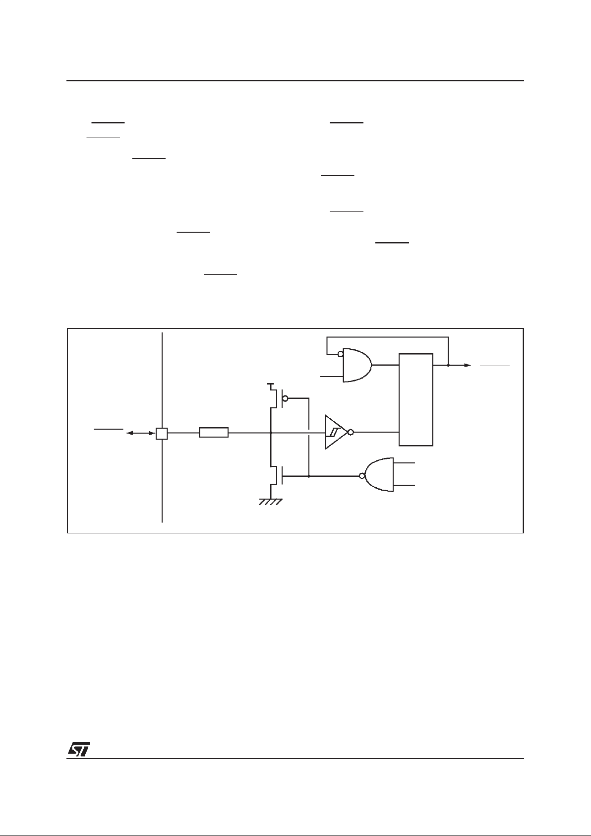
Figure 14. Reset Block Diagram
f
INT
COUNTER
RESET
WATCHDOG RESET
LVD RESET
INTERNAL
RESET
R
ESD
1)
1) Resistive ESD protection
V
DD
R
PU
2048 clock cycles
1
Page 26
ST6208C/ST6209C/ST6210C/ST6220C
26/105
RESET (Cont’d)
5.3.4 Watchdog Reset
The MCU provides a Watchdog timer function in
order to be able to recover from software hangups. If the Watchdog register is not refreshed before an end-of-count condition is reached, a
Watchdog reset is generated.
After a Watchdog reset, the MCU restarts in the
same way as if a Reset was generated by the RESET pin.
Note: When a watchdog reset occurs, the RESET
pin is tied low for very short time period, to flag the
reset phase. This time is not long enough to reset
external circuits.
For more details refer to the Watchdog Timer
chapter.
5.3.5 LVD Reset
Two different RESET sequences caused bythe internal LVD circuitry can be distinguished:
■ Power-On RESET
■ Voltage Drop RESET
During an LVD reset, the RESET pin is pulled low
when VDD<V
IT+
(rising edge) or VDD<V
IT-
(falling
edge).
For more details, refer to the LVD chapter.
Caution: Do not externally connect directly the
RESET pin to VDD, this may cause damage to the
component in case of internal RESET (Watchdog
or LVD).
Figure 15. Simple external Reset Circuitry
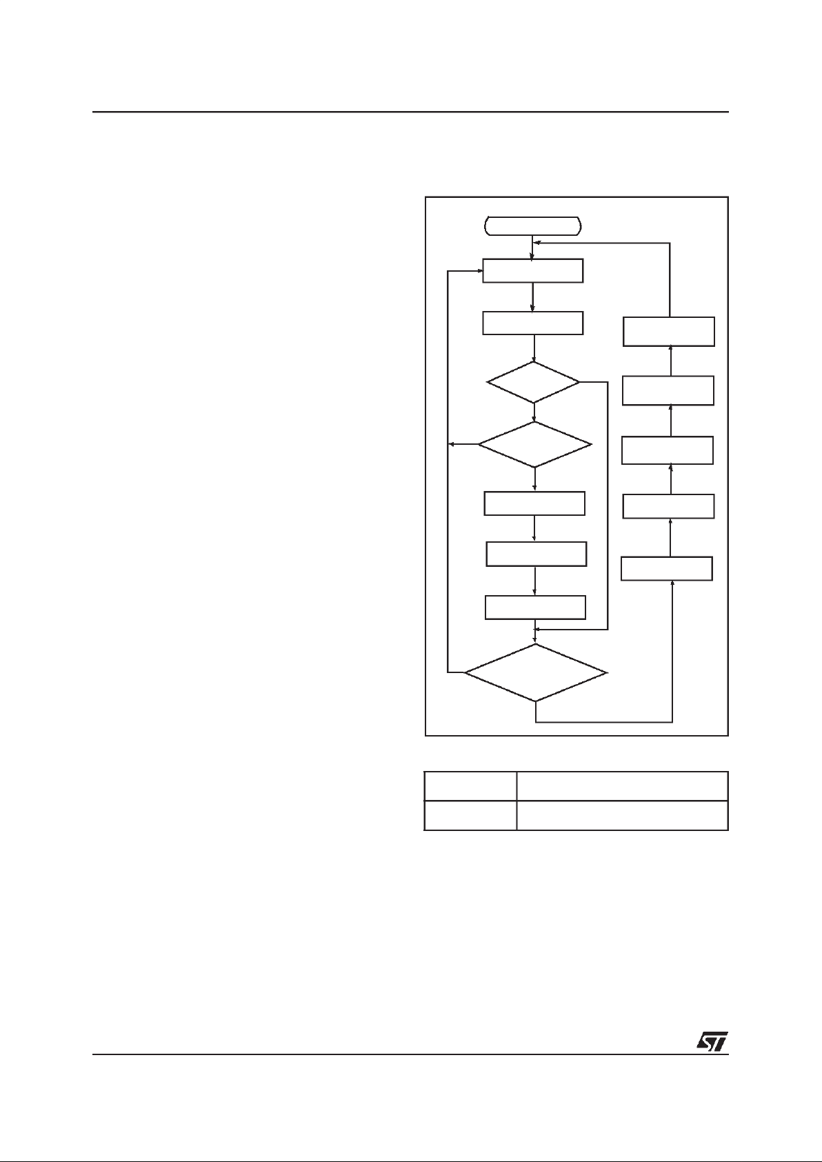
Figure 16. Reset Processing
ST62xx
RESET
V
DD
V
DD
R
C
Typical: R = 10K
C = 10nF
R > 4.7 K
INT LATCH CLEARED
NMI MASK SET
(IF PRESENT)
SELECT
NMI MODE FLAGS
IS RESET STILL
PRESENT?
YES
PUT FFEh
ON ADDRESS BUS
FROM RESET LOCATIONS
FFEh/FFFh
NO
FETCH INSTRUCTION
LOAD PC
INTERNAL
RESET
RESET
2048
CLOCK CYCLE
DELAY
1
Page 27
ST6208C/ST6209C/ST6210C/ST6220C
27/105
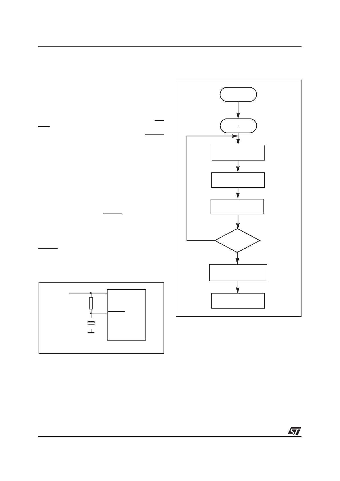
6 INTERRUPTS
The ST6 core may be interrupted by four maskable interrupt sources, in addition to a Non Maskable Interrupt (NMI) source. The interrupt processing flowchartis shown in Figure 18.
Maskable interrupts must be enabled by setting
the GEN bit in the IOR register. However, even if
they are disabled (GEN bit = 0), interrupt events
are latchedand may be processed as soon as the
GEN bit is set.
Each source is associated with a specific Interrupt
Vector, locatedin Program space (seeTable 8). In
the vector location, the user must write a Jump in-
struction to the associated interrupt service routine.
When an interrupt source generates an interrupt
request, the PC register is loaded with the address
of the interrupt vector, which then causes a Jump
to the relevant interrupt service routine, thus servicing the interrupt.
Interrupt are triggered byevents either on external
pins, or from the on-chip peripherals. Several
events can be ORed on the same interrupt vector.
On-chip peripherals have flag registers to determine which event triggered the interrupt.
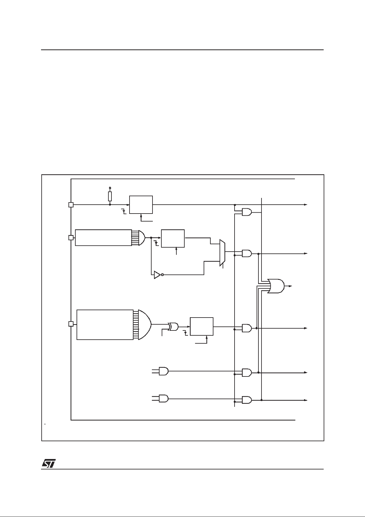
Figure 17. Interrupts Block Diagram
NMI
ESB BIT
V
DD
LATCH
CLEARED BY H/W
AT START OF VECTOR #0 ROUTINE
VECTOR #0
LES BIT
1
0
LATCH
CLEARED BY H/W
AT START OF
VECTOR #1
VECTOR#2
VECTOR #3
VECTOR #4
LATCH
CLEARED
BY H/W AT START OF
VECTOR #2 ROUTINE
I/O PORT REGISTER
CONFIGURATION
“INPUT WITH INTERRUPT”
I/O PORT REGISTER
CONFIGURATION
“INPUT WITH INTERRUPT”
EXIT FROM
STOP/WAI T
VECTOR #1 ROUTINE
TIMER
A/D CONVERTER *
TMZ BIT
ETI BIT
EAI BIT
EOC BIT
GEN BIT
PB0...PB7
PA0...PA3
(TSCR REGISTER)
(ADCR REGISTER)
(IOR REGISTER)
(IOR REGISTER)
(IOR REGISTER)
* Depending on device. See device summary on page 1.
1
Page 28

ST6208C/ST6209C/ST6210C/ST6220C
28/105
6.1 INTERRUPT RULES AND PRIORITY
MANAGEMENT
■ A Reset can interrupt the NMI and peripheral
interrupt routines
■ The Non Maskable Interrupt request has the
highest priority and can interrupt any peripheral
interrupt routine at any time but cannot interrupt
another NMI interrupt.
■ No peripheral interrupt can interrupt another. If
more than one interrupt request is pending,
these are processed by the processor core
according to their priority level: vector#1 has the
highest priority while vector #4 the lowest. The
priority of each interrupt source is fixed by
hardware (see Interrupt Mapping table).
6.2 INTERRUPTS AND LOW POWER MODES
All interrupts cause the processor to exit from
WAIT mode. Only the external and some specific
interrupts from the on-chip peripherals cause the
processor to exit from STOP mode (refer to the
“Exit from STOP“ column in the Interrupt Mapping
Table).
6.3 NON MASKABLE INTERRUPT
This interrupt is triggered when a falling edge occurs on the NMI pin regardless of the state of the
GEN bit in the IOR register. An interrupt request
on NMI vector #0 is latched by a flip flop which is
automatically reset by the core at the beginning of
the NMI service routine.
6.4 PERIPHERAL INTERRUPTS
Different peripheral interrupt flags in the peripheral
control registers are able to cause an interrupt
when they are active if both:
– The GEN bit of the IOR register is set
– Thecorresponding enable bit is set in the periph-
eral control register.
Peripheral interrupts are linked to vectors #3 and
#4. Interrupt requests are flagged by a bit in their
corresponding control register. This means that a
request cannot be lost, because the flag bit must
be cleared by user software.
1
Page 29

ST6208C/ST6209C/ST6210C/ST6220C
29/105
6.5 EXTERNAL INTERRUPTS (I/O Ports)
External interrupt vectors can be loaded into the
PC register if the corresponding external interrupt
occurred and if the GEN bit is set. These interrupts
allow the processor to exit from STOP mode.
The external interrupt polarity is selected through
the IOR register.
External interrupts are linked to vectors #1 and #
2.
Interrupt requests on vector #1 can be configured
either as edge or level-sensitive using the LES bit
in the IOR Register.
Interrupt requests from vector #2 are always edge
sensitive. The edge polarity can be configured using the ESB bit in the IOR Register.
In edge-sensitive mode, a latch is set when a edge
occurs on the interrupt source line and is cleared
when the associated interrupt routine is started.
So, an interrupt request can be stored until completion of the currently executing interrupt routine,
before being processed. If several interrupt requests occurs before completion of the current interrupt routine, only the first request is stored.
Storing ofinterrupt requests is not possible in level
sensitive mode. To be taken into account, the low
level must be present on the interrupt pin when the
MCU samples the line after instruction execution.
6.5.1 Notes on using External Interrupts
ESB bit Spurious Interrupt on Vector #2
If a pin associated with interrupt vector #2 is configured as interrupt with pull-up, whenever vector
#2 is configured tobe rising edge sensitive (by setting the ESB bit in the IOR register), an interrupt is
latched although a rising edge may not have occured on the associated pin.
This is due to the vector #2 circuitry.The workaround is to discard this first interrupt request in the
routine (using a flag for example).
Masking of One Interrupt by Another on Vector
#2.
When two or moreport pins (associated with interrupt vector #2) are configured together as input
with interrupt (falling edge sensitive), as long as
one pin is stuck at ’0’,the other pin cannever generate an interrupt even if an active edge occurs at
this pin. The same thing occurs when one pin is
stuck at ’1’and interrupt vector #2 is configured as
rising edge sensitive.
To avoid this the first pin must input a signal that
goes back upto ’1’ right after the falling edge. Otherwise, in the interrupt routine for the first pin, deactivate the “input with interrupt” mode using the
port control registers (DDR, OR, DR). An active
edge on another pin can then be latched.
I/O port Configuration Spurious Interrupt on
Vector #2
If a pin associated with interrupt vector #2 is in ‘input with pull-up’ state, a ‘0’ level is present on the
pin and the ESB bit= 0, when the I/O pin is configured as interrupt with pull-up by writing to the
DDRx, ORx and DRx register bits, an interrupt is
latched although a falling edge may not have occurred on the associated pin.
In the opposite case, if the pin is in interrupt with
pull-up state , a 0 level is present on the pin and
the ESB bit =1, when the I/O port is configured as
input with pull-up by writing to the DDRx, ORxand
DRx bits, an interrupt is latched although a rising
edge may not have occurred on the associated
pin.
1
Page 30
ST6208C/ST6209C/ST6210C/ST6220C
30/105
6.6 INTERRUPT HANDLING PROCEDURE
The interrupt procedure isvery similar to a callprocedure, in fact the user can consider the interrupt
as an asynchronous call procedure. As this is an
asynchronous event, the user cannot know the
context and the time at which it occurred. As a result, the user should save all Data space registers
which may be used within the interrupt routines.
The following list summarizes the interrupt procedure:
When an interrupt request occurs, the following
actions are performed by the MCU automatically:
– The core switches from the normal flags to the
interrupt flags (or the NMI flags).
– ThePC contents arestored inthe top level ofthe
stack.
– The normal interrupt lines are inhibited (NMI still
active).
– The internal latch (if any) is cleared.
– TheassociatedinterruptvectorisloadedinthePC.
When an interrupt request occurs, the following
actions must be performed by the user software:
– User selected registers have to be saved within
the interrupt service routine (normally ona soft-
ware stack).
– The source of the interrupt must be determined
by polling the interrupt flags (if more than one
source is associated with the same vector).
– The RETI (RETurn from Interrupt) instruction
must end the interrupt service routine.
After the RETI instruction isexecuted, the MCU re-
turns to the main routine.
Caution: When a maskable interrupt occurs while
the ST6 core is in NORMAL mode and during the
execution of an “ldi IOR, 00h”instruction (disabling
all maskable interrupts): if the interrupt request occurs during the first 3 cycles of the “ldi” instruction
(which is a 4-cycle instruction) the core will switch
to interrupt mode BUT the flags CN and ZN will
NOT switch to the interrupt pair CI and ZI.
6.6.1 Interrupt Response Time
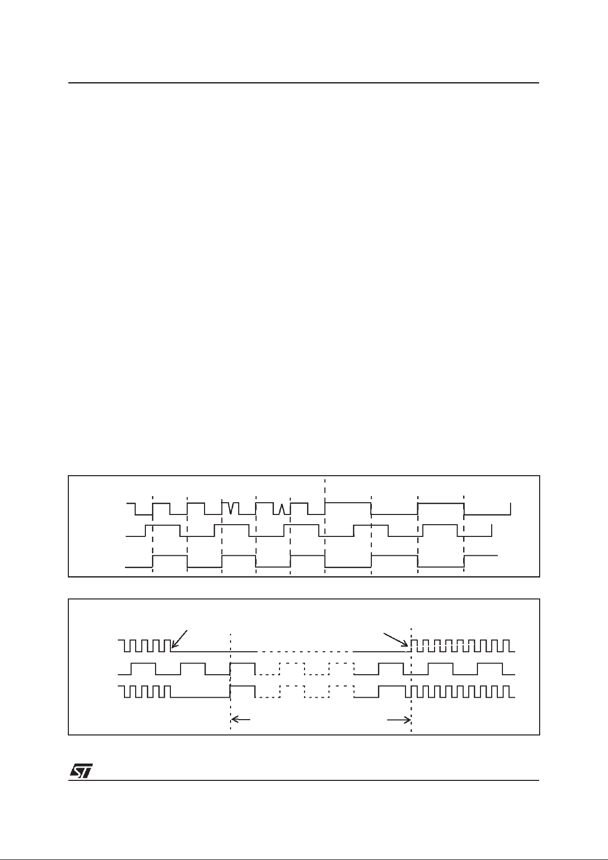
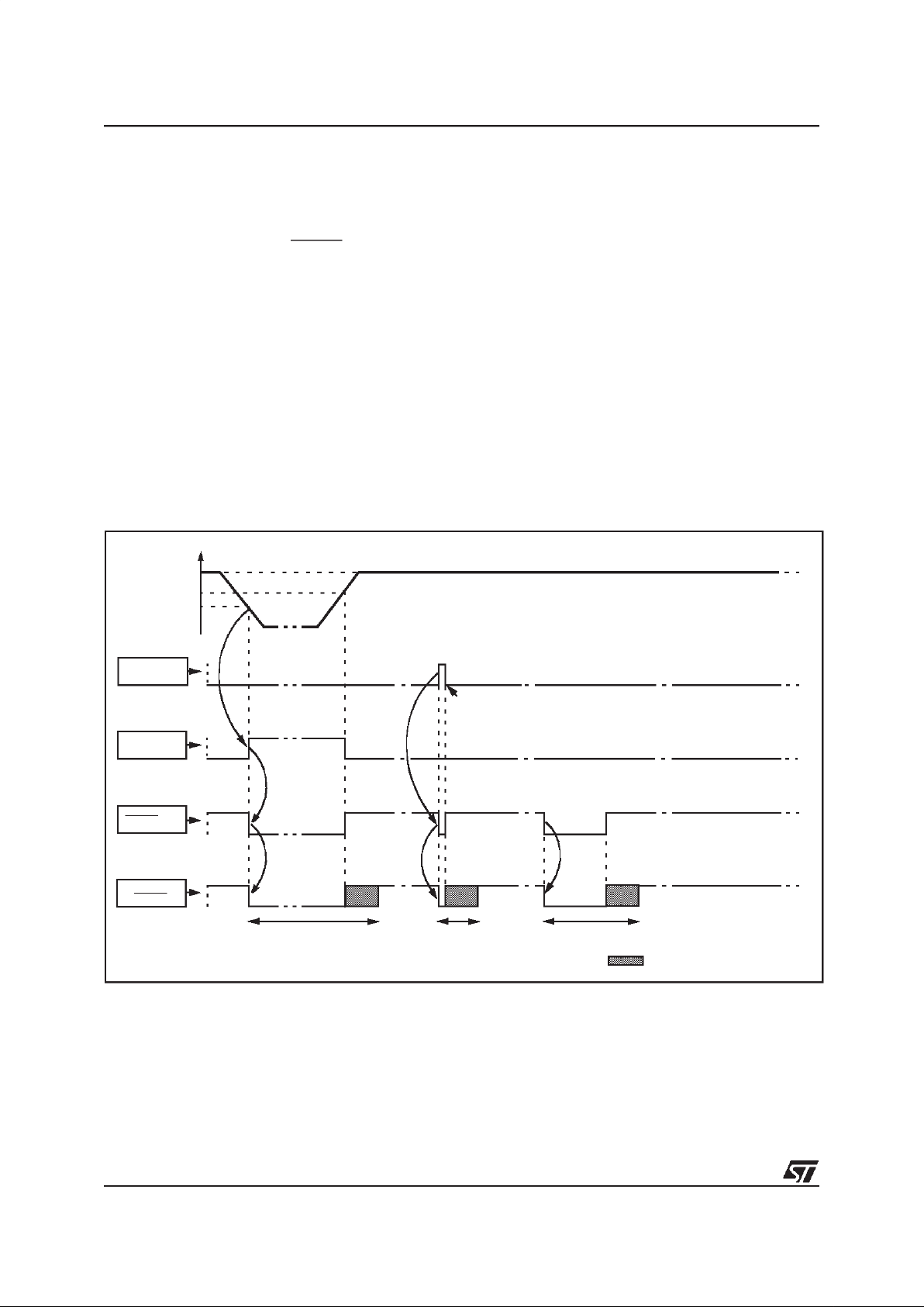
This is defined as the time between the moment
when the Program Counter is loaded with the interrupt vector and when the program has jump to
the interrupt subroutine and is ready to execute
the code. It depends on when the interrupt occurs
while the core is processing an instruction.
Figure 18. Interrupt Processing Flow Chart
Table 7. Interrupt Response Time
One CPU cycle is 13 external clock cycles thus 11
CPU cycles = 11 x (13 /8M) = 17.875 µs with an 8
MHz external quartz.
Minimum 6 CPU cycles
Maximum 11 CPU cycles
INSTRUCTION
FETCH
INSTRUCTION
EXECUTE
INSTRUCTION
WAS
THE INSTRUCTION
A RETI?
ENABLE
MASKABLE INTERRUPTS
SELECT
NORMAL FLAGS
“POP”
THE STACKED PC
IS THERE AN
AN INTERRUPT REQUEST
AND INTERRUPT MASK?
SELECT
INTERRUPT FLAGS
PUSH THE
PC INTO THE STACK
LOAD PC FROM
INTERRUPT VECTOR
DISABLE
MASKABLE INTERRUPT
NO
NO
YES
IS THE CORE
ALREADY IN
NORMAL MODE?
YES
NO
YES
CLEAR
INTERNAL LATCH
*)
*)
If a latch is present on the interrupt source line
1
Page 31

ST6208C/ST6209C/ST6210C/ST6220C
31/105
6.7 REGISTER DESCRIPTION
INTERRUPT OPTION REGISTER (IOR)
Address: 0C8h — Write Only
Reset status: 00h
Caution: This register is write-only and cannot be
accessed by single-bit operations (SET, RES,
DEC,...).
Bit 7 =Reserved, must be cleared.
Bit 6 = LES
Level/Edge Selection bit
.
0: Falling edge sensitivemode is selected for inter-
rupt vector #1
1: Low level sensitive mode is selected for inter-
rupt vector #1
Bit 5 = ESB
Edge Selection bit
.
0: Falling edge mode on interrupt vector #2
1: Rising edge mode on interrupt vector #2
Bit 4 = GEN
Global Enable Interrupt
.
0: Disable all maskable interrupts
1: Enable all maskable interrupts
Note: When the GEN bit iscleared, the NMI interrupt isactive but cannot be used toexit from STOP
or WAIT modes.
Bits 3:0 = Reserved, must be cleared.
Table 8. Interrupt Mapping
* Depending on device. See device summary on page 1.
70
- LES ESB GEN - - - -
Vector
number
Source
Block
Description
Register
Label
Flag
Exit
from
STOP
Vector
Address
Priority
Order
RESET Reset N/A N/A yes FFEh-FFFh
Vector #0 NMI Non Maskable Interrupt N/A N/A yes FFCh-FFDh
NOT USED
FFAh-FFBh
FF8h-FF9h
Vector #1 Port A Ext. Interrupt Port A N/A N/A yes FF6h-FF7h
Vector #2 Port B Ext. Interrupt Port B N/A N/A yes FF4h-FF5h
Vector #3 TIMER Timer underflow TSCR TMZ yes FF2h-FF3h
Vector #4 ADC* End Of Conversion ADCR EOC no FF0h-FF1h
Priority
Lowest
Highest
Priority
1
Page 32

ST6208C/ST6209C/ST6210C/ST6220C
32/105
7 POWER SAVING MODES
7.1 INTRODUCTION
To give a large measure of flexibilityto the application in terms of power consumption, two mainpower saving modes are implemented in the ST6 (see
Figure 19).
In addition, theLow Frequency Auxiliary Oscillator
(LFAO) can be used instead of the main oscillator
to reduce power consumption in RUN and WAIT
modes.
After a RESET the normal operating mode is selected by default (RUN mode). This mode drives
the device (CPU and embedded peripherals) by
means of a master clock which is based on the
main oscillator frequency.
From Run mode, the different power saving
modes may be selected by calling the specific ST6
software instruction or for the LFAO by setting the
relevant register bit. For more information on the
LFAO, please refer to the Clock chapter.
Figure 19. Power Saving Mode Transitions
POWER CONSUMPTION
WAIT
LFAO
RUN
STOP
High
Low
1
Page 33

ST6208C/ST6209C/ST6210C/ST6220C
33/105
7.2 WAIT MODE
The MCU goes into WAIT mode as soon as the
WAIT instruction is executed. This has the following effects:
– Program execution is stopped, the microcontrol-
ler software can be considered as being in a “frozen” state.
– RAM contents and peripheral registers are pre-
served as long as the power supply voltage is
higher than the RAM retention voltage.
– The oscillator is kept running to provide a clock
to the peripherals; they are still active.
WAIT mode can be used when the user wants to
reduce the MCU power consumption during idle
periods, while not losing track of time or the ability
to monitor external events. WAIT mode places the
MCU in a low power consumption mode by stopping the CPU. Theactive oscillator (main oscillator
or LFAO) is keptrunning in order to provide aclock
signal to the peripherals.
If the power consumption has to be further reduced, the Low Frequency Auxiliary Oscillator
(LFAO) can be used in place of the main oscillator,
if its operating frequency is lower. If required, the
LFAO must be switched on before entering WAIT
mode.
Exit from Wait mode
The MCU remains in WAIT mode until one of the
following events occurs:
– RESET (Watchdog, LVD or RESET pin)
– A peripheral interrupt (timer, ADC,...),
– An external interrupt (I/O port, NMI)
The Program Counter then branches to the starting address of the interrupt or RESET service routine. Refer to Figure 20.
Note: It should be noted that when the GEN bit in
the IOR register is low (interrupts disabled), the
NMI interrupt is active but cannot causea wake up
from STOP/WAIT modes.
Figure 20. WAIT Mode Flow-chart
WAIT INSTRUCTION
RESET
INTERRUPT
Y
N
N
Y
Clock to CPU
OSCILLATOR
Clock to PERIPHERALSOnYes
No
FETCH RESET VECTOR
OR SERVICE INTERRUPT
2048 CLOCK CYCLE
DELAY
Clock to CPU
OSCILLATOR
Clock to PERIPHERALS
Restart
Yes
Yes
Clock to CPU
OSCILLATOR
Clock to PERIPHERALSOnYes
Yes
1
Page 34

ST6208C/ST6209C/ST6210C/ST6220C
34/105
7.3 STOP MODE
STOP mode is the lowest power consumption
mode of the MCU (see Figure 22).
The MCU goes into STOP mode as soon as the
STOP instruction is executed. This has the following effects:
– Program execution is stopped, the microcontrol-
ler can be considered as being “frozen”.
– The contents of RAM and the peripheral regis-
ters are kept safely as long as the power supply
voltage is higher than the RAM retention voltage.
– The oscillator is stopped, so peripherals cannot
work except the those that can be driven by an
external clock.
Exit from STOP mode
The MCU remains in STOP mode until one of the
following events occurs:
– RESET (Watchdog, LVD or RESET pin)
– A peripheral interrupt (assuming this peripheral
can be driven by an external clock)
– An external interrupt (I/O port, NMI)
In all cases a delay of 2048 clock cycles (f
INT
)is
generated to make sure the oscillator has started
properly.
The Program Counter then points to the starting
address of the interrupt or RESET service routine
(see Figure 21).
STOP mode and Watchdog
When the Watchdog is active (hardware or software activation), the STOP instruction is disabled
and a WAIT instructionwill be executed in its place
unless the EXCTNL option bitis set to 1in the option bytes and a a high level is present on the NMI
pin. In this case, the STOP instruction will be executed and the Watchdog will be frozen.
Figure 21. STOP Mode Timing Overview
STOPRUN RUN
2048 CLOCK CYCLE
DELAY
RESET
OR
INTERRUPT
STOP
INSTRUCTION
FETCH
VECTOR
1
Page 35

ST6208C/ST6209C/ST6210C/ST6220C
35/105
STOP MODE (Cont’d)
Figure 22. STOP Mode Flow-chart
Notes:
1. EXCTNL is an option bit. See option byte section for more details.
2. Peripheral clocked with an external clock source can still be active.
3. Only some specific interrupts can exit the MCU from STOP mode (such as external interrupt). Refer to
the Interrupt Mapping table for more details.
STOP INSTRUCTION
RESET
INTERRUPT
3)
Y
N
N
Y
FETCH RESET VECTOR
OR SERVICE INTERRUPT
WATCHDOG
ENABLE
DISABLE
EXCTNL
1
1
LEVEL
ON
NMI PIN
0
0
RESET
INTERRUPT
N
N
Y
Y
VALUE
1)
Clock to CPU
OSCILLATOR
Clock to PERIPHERALS
2)
Off
No
No
2048 CLOCK CYCLE
DELAY
Clock to CPU
OSCILLATOR
Clock to PERIPHERALS
Restart
Yes
Yes
Clock to CPU
OSCILLATOR
Clock to PERIPHERALSOnYes
Yes
Clock to CPU
OSCILLATOR
Clock to PERIPHERALSOnYes
No
1
Page 36

ST6208C/ST6209C/ST6210C/ST6220C
36/105
7.4 NOTES RELATED TO WAIT AND STOP MODES
7.4.1 Exit from Wait and Stop Modes
7.4.1.1 NMI Interrupt
It should be noted that when the GEN bit in the
IOR register is low (interrupts disabled), the NMI
interrupt is active butcannot cause a wake upfrom
STOP/WAIT modes.
7.4.1.2 Restart Sequence
When the MCU exits from WAIT or STOP mode, it
should be noted that the restart sequence depends on the original stateof the MCU (normal, interrupt or non-maskable interrupt mode) prior to
entering WAIT or STOP mode, as well as on the
interrupt type.
Normal Mode. If the MCU was in the main routine
when the WAIT or STOP instruction was executed, exit from Stop or Wait mode will occur as soon
as an interrupt occurs; the related interrupt routine
is executed and, on completion, the instruction
which follows the STOP or WAIT instruction is
then executed, providing no other interrupts are
pending.
Non Maskable Interrupt Mode. If the STOP or
WAIT instruction has been executed during execution of the non-maskable interrupt routine, the
MCU exits from Stop or Wait mode as soon as an
interrupt occurs: the instruction which follows the
STOP or WAIT instruction is executed, and the
MCU remains in non-maskable interrupt mode,
even if another interrupt has been generated.
Normal Interrupt Mode. If the MCU was in interrupt mode before the STOP or WAIT instruction
was executed, it exits from STOP or WAIT mode
as soon as an interrupt occurs. Nevertheless, two
cases must be considered:
– If the interrupt is a normal one, the interrupt rou-
tine in which the WAIT or STOP mode was entered will be completed, starting with the
execution of the instruction which follows the
STOP or the WAIT instruction, and the MCU is
still in interrupt mode. At the end of this routine
pending interrupts will be serviced according to
their priority.
– In the event of a non-maskable interrupt, the
non-maskable interrupt service routine is processed first,then the routine inwhich the WAIT or
STOP mode was entered will be completed by
executing the instruction following the STOP or
WAIT instruction.The MCU remains in normalinterrupt mode.
7.4.2 Recommended MCU Configuration
For lowest power consumption during RUN or
WAIT modes, the user software must configure
the MCU as follows:
– Configure unused I/Os as inputs without pull-up
(these should be externally tied to well-defined
logic levels)
– Place all peripherals in their power down modes
before entering STOP mode
– Select the Low Frequency Auxiliary Oscillator
(provided this runs at a lowerfrequency than the
main oscillator).
The WAIT and STOP instructions are not executed if an enabled interrupt request is pending.
1
Page 37

ST6208C/ST6209C/ST6210C/ST6220C
37/105
8 I/O PORTS
8.1 INTRODUCTION
Each I/O port contains up to 8 pins. Each pin can
be programmed independently as digital input
(with or without pull-up and interrupt generation),
digital output (open drain, push-pull) or analog input (when available).
The I/O pins can be used in either standard or alternate function mode.
Standard I/O mode is used for:
– Transfer of data through digital inputsand out-
puts (on specific pins):
– External interrupt generation
Alternate function mode is used for:
– Alternate signal input/output for the on-chip
peripherals
The generic I/O block diagram is shown in Figure
23.
8.2 FUNCTIONAL DESCRIPTION
Each port is associated with 3 registers located in
Data space:
– Data Register (DR)
– Data Direction Register (DDR)
– Option Register (OR)
Each I/Opin may be programmed using the corre-
sponding register bits in the DDR, DR and OR registers: bit x corresponding topin xof theport. Table
9 illustrates the various port configurations which
can be selected by user software.
During MCU initialization, all I/O registers are
cleared and the input mode with pull-up and no interrupt generation is selected for all the pins, thus
avoiding pin conflicts.
8.2.1 Digital input modes
The input configuration is selected by clearing the
corresponding DDR register bit.
In this case, reading the DR register returns the
digital value applied to the external I/O pin.
Different input modes can be selected by software
through the DR and OR registers, see Table 9.
External interrupt function
All input lines can be individually connected by
software to the interrupt system by programming
the OR and DR registers accordingly. The interrupt trigger modes (falling edge, rising edge and
low level) can be configured by software for each
port as described in the Interrupt Chapter.
8.2.2 Analog inputs
Some pins can be configured as analog inputs by
programming the OR and DR registers accordingly, see Table 9. These analog inputs are connected to the on-chip 8-bit Analog to Digital Converter.
Warning: ONLY ONE pin should be programmed
as an analog input at any time, since by selecting
more than one input simultaneously their pins will
be effectively shorted.
8.2.3 Output modes
The output configuration is selected by setting the
corresponding DDR register bit. In this case, writing to the DR register applies this digital value to
the I/Opin through the latch. Then, readingthe DR
register returns the previously stored value.
Two different output modes can be selected by
software through the OR register: push-pull and
open-drain.
DR register value and output pin status:
Note: The open drain setting is not a true open
drain. This means it has the same structure as the
push-pull setting but the P-buffer is deactivated.
8.2.4 Alternate functions
When an on-chip peripheral is configured to use a
pin, the alternate function (timer input/output...) is
not systematically selected but has to be configured through the DDR, OR and DR registers. Refer to the chapter describing the peripheral for
more details.
DR Push-pull Open-drain
0V
SS
V
SS
1VDDFloating
1
Page 38

ST6208C/ST6209C/ST6210C/ST6220C
38/105
I/O PORTS (Cont’d)
Figure 23. I/O Port Block Diagram
Table 9. I/O Port Configurations
Note: x = Don’t care
DDR OR DR Mode Option
0 0 0 Input With pull-up, no interrupt
0 0 1 Input No pull-up, no interrupt
0 1 0 Input With pull-up and with interrupt
0 1 1 Input Analog input (when available)
1 0 x Output Open-drain output (20mA sink when available)
1 1 x Output Push-pull output (20mA sink when available)
V
DD
RESET
ST6
INTERNAL
DATA
DATA
DIRECTION
REGISTER
REGISTER
OPTION
REGISTER
TO INTERRUPT
V
DD
TO ADC
V
DD
N-BUFFER
P-BUFFER
PULL-UP
CMOS
SCHMITT
TRIGGER
PxxI/OPin
BUS
CLAMPING
DIODES
*
* Depending on device. See device summary on page 1.
1
Page 39

ST6208C/ST6209C/ST6210C/ST6220C
39/105
I/O PORTS (Cont’d)
8.2.5 Instructions NOT to be used to access
Port Data registers (SET, RES, INC and DEC)
DO NOT USE SINGLE-BIT INSTRUCTIONS
(SET, RES, INC and DEC) ON PORT DATA REGISTERS IF ANY PIN OF THE PORT IS CONFIGURED IN INPUT MODE.
These instructions make an implicit read and write
back of the entire register. In port input mode,
however, the data register reads from the input
pins directly, and not from the data register latches. Since data register information in input mode is
used to set the characteristics of the input pin (interrupt, pull-up, analog input), these may be unintentionally reprogrammed depending on the state
of the input pins.
As a general rule, it is better to only use single bit
instructions on data registers when the whole (8bit) port is in output mode. In the case of inputs or
of mixed inputs and outputs,it is advisable to keep
a copy of the data register in RAM. Single bit instructions may then be used on the RAM copy, after which the whole copy register can bewritten to
the port data register:
SET bit, datacopy
LD a, datacopy
LD DRA, a
8.2.6 Recommendations
1. Safe I/O State Switching Sequence
Switching the I/O ports from one state to another
should be done in a sequence which ensures that
no unwanted side effects can occur. The recommended safetransitions areillustrated in Figure 24
All other transitions are potentially risky and
should be avoided when changing the I/O operating mode.
2. Handling Unused Port Bits
On ports that have less than 8 external pins connected:
– Leave the unbonded pins in reset state and do
not change their configuration.
– Do not use instructions that act on a whole port
register (INC,DEC, or read operations).Unavailable bits must be masked by software (AND instruction). Thus, when a read operation
performed onan incomplete port is followedby a
comparison, use a mask.
3. High Impedance Input
On any CMOS device, it is not recommended to
connect high impedance on input pins. The choice
of these impedance has to be done with respect to
the maximum leakage current defined in the datasheet. The risk is to be close or out of specification on the input levels applied to the device.
8.3 LOW POWER MODES
The WAIT and STOP instructions allow the
ST62xx to be used in situations where low power
consumption is needed. The lowest power consumption is achieved by configuring I/Os in output
push-pull low mode.
8.4 INTERRUPTS
The external interrupt event generates an interrupt
if the corresponding configuration is selected with
DDR, DR and OR registers (see Table 9) and the
GEN-bit in the IOR register is set.
Figure 24. Diagram showing Safe I/O State Transitions
Note *. xxx = DDR, OR, DR Bits respectively
Mode Description
WAIT
No effect on I/O ports. External interrupts
cause the device to exit from WAIT mode.
STOP
No effect on I/O ports. External interrupts
cause the device to exit from STOP mode.
Interrupt
pull-up
Output
Open Drain
Output
Push-pull
Input
pull-up (Reset
state)
Input
Analog
Output
Open Drain
Output
Push-pull
Input
010*
000
100
110
011
001
101
111
1
Page 40

ST6208C/ST6209C/ST6210C/ST6220C
40/105
I/O PORTS (Cont’d)
Table 10. I/O Port Option Selections
Note 1. Provided the correct configuration has been selected (see Table 9).
MODE AVAILABLE ON
(1)
SCHEMATIC
Digital Input
Input
PA0-PA3
PB0-PB7
DDRx0ORx0DRx
1
Reset state
Input
with pull up
PA0-PA3
PB0-PB7
DDRx0ORx0DRx
0
Input
with pull up
with interrupt
PA0-PA3
PB0-PB7
DDRx0ORx1DRx
0
Analog Input
Analog Input
PB0-PB3
(ST6210C/20C)
PB4-PB7
(except ST6208C)
DDRx0ORx1DRx
1
Digital output
Open drain output (5mA)
Open drain output (20 mA)
PB0-PB7
PA0-PA3
DDRx1ORx0DRx
0/1
Push-pull output (5mA)
Push-pull output (20 mA)
PB0-PB7
PA0-PA3
DDRx1ORx1DRx
0/1
Data in
Interrupt
V
DD
V
DD
Data in
Interrupt
V
DD
V
DD
Data in
Interrupt
V
DD
V
DD
ADC
V
DD
Data out
P-buffer disconnected
V
DD
Data out
V
DD
1
Page 41

ST6208C/ST6209C/ST6210C/ST6220C
41/105
I/O PORTS (Cont’d)
8.5 REGISTER DESCRIPTION
DATA REGISTER (DR)
Port x Data Register
DRx with x = A orB.
Read/Write
Reset Value: 0000 0000 (00h)
Bits 7:0 = D[7:0]
Data register bits.
Reading theDR register returns either the DR register latch content (pin configured as output) or the
digital value applied to the I/O pin (pin configured
as input).
Caution: In input mode, modifying this register will
modify the I/O port configuration (see Table 9).
Do not use the Single bit instructions on I/O port
data registers. See (Section 8.2.5).
DATA DIRECTION REGISTER (DDR)
Port x Data Direction Register
DDRx with x = A or B.
Read/Write
Reset Value: 0000 0000 (00h)
Bits 7:0 = DD[7:0]
Data direction register bits.
The DDR register gives the input/output direction
configuration of the pins. Each bit is set and
cleared by software.
0: Input mode
1: Output mode
OPTION REGISTER (OR)
Port x Option Register
ORx with x = A or B.
Read/Write
Reset Value: 0000 0000 (00h)
Bits 7:0 = O[7:0]
Option register bits.
The OR register allows to distinguish in output
mode if the push-pull or open drain configuration is
selected.
Output mode:
0: Open drain output(with P-Buffer deactivated)
1: Push-pull Output
Input mode: See Table 9.
Each bit is set and cleared by software.
Caution: Modifying this register, will also modify
the I/O port configuration in input mode. (see Table 9).
Table 11. I/O Port Register Map and Reset Values
70
D7 D6 D5 D4 D3 D2 D1 D0
70
DD7 DD6 DD5 DD4 DD3 DD2 DD1 DD0
70
O7 O6 O5 O4 O3 O2 O1 O0
Address
(Hex.)
Register
Label
76543210
Reset Value
of all I/O port registers
00000000
0C0h DRA
MSB LSB
0C1h DRB
0C4h DDRA
MSB LSB
0C5h DDRB
0CCh ORA
MSB LSB
0CDh ORB
1
Page 42

ST6208C/ST6209C/ST6210C/ST6220C
42/105
9 ON-CHIP PERIPHERALS
9.1 WATCHDOG TIMER (WDG)
9.1.1 Introduction
The Watchdog timer is used to detect the occurrence of a software fault, usually generated by external interference or by unforeseen logical conditions, which causes the application program to
abandon its normal sequence. The Watchdog circuit generates an MCU reset on expiry of a programmed timeperiod, unless the program refreshes the counter’s contents before the SR bit becomes cleared.
9.1.2 Main Features
■ Programmable timer (64 steps of 3072 clock
cycles)
■ Software reset
■ Reset (if watchdog activated) when the SR bit
reaches zero
■ Hardware or software watchdog activation
selectable by option bit (Refer to the option
bytes section)
Figure 25. Watchdog Block Diagram
RESET
C
7-BIT DOWNCOUNTER
f
int /12
SR
T0
CLOCK DIVIDER
WATCHDOG REGISTER (WDGR)
÷ 256
T1
T2
T3
T4
T5
bit 0
bit 7
1
Page 43

ST6208C/ST6209C/ST6210C/ST6220C
43/105
WATCHDOG TIMER (Cont’d)
9.1.3 Functional Description
The watchdog activation is selected through an
option in the option bytes:
– HARDWARE watchdog option
After reset, the watchdog is permanently active,
the C bit in the WDGR is forced high and the user
can not change it. However, this bit can be read
equally as 0 or 1.
– SOFTWARE watchdog option
After reset, the watchdog is deactivated. The func-
tion is activated by setting C bit in the WDGR register. Once activated, it cannot be deactivated.
The counter value stored in the WDGR register
(bits SR:T0), is decremented every 3072 clock cycles. The length of the timeout period can be programmed bythe user in 64 steps of 3072 clock cycles.
If the watchdog is activated (by setting the C bit)
and when the SR bit is cleared, the watchdog initiates a reset cycle pulling the reset pin low for typically 500ns.
The application program must write in the WDGR
register at regular intervals during normal operation to prevent an MCU reset. The value to be
stored in the WDGR register must be between
FEh and 02h (see Table 12). To run the watchdog
function the following conditions must be true:
– The C bitis set (watchdog activated)
– The SR bit is set toprevent generating an imme-
diate reset
– The T[5:0] bits contain the number of decre-
ments which represent the time delay before the
watchdog produces a reset.
Table 12. Watchdog Timing (f
OSC
= 8 MHz)
9.1.3.1 Software Reset
The SR bit can beused to generate a software reset by clearing the SR bit while the C bit is set.
9.1.4 Recommendations
1. The Watchdog plays an important supporting
role in the high noise immunity ofST62xx devices,
and should be used wherever possible. Watchdog
related options should be selected on the basis of
a trade-off between application security and STOP
mode availability (refer to the description of the
WDACT and EXTCNTL bits on theOption Bytes).
When STOP mode is not required, hardware activation without EXTERNAL STOP MODE CONTROL should be preferred, as it provides maximum security, especially during power-on.
When STOP mode is required, hardware activation and EXTERNAL STOP MODE CONTROL
should be chosen. NMI should be high by default,
to allow STOP mode to be entered when theMCU
is idle.
The NMI pin can be connected to an I/O line (see
Figure 26)to allow its stateto be controlledby software. The I/O line can then be used to keep NMI
low while Watchdog protection is required, or to
avoid noise or key bounce. When no more
processing is required, the I/O line is released and
the device placed in STOP mode for lowestpower
consumption.
Figure 26. A typical circuit making use of the
EXERNAL STOP MODE CONTROL feature
2. When software activation is selected (WDACT
bit in Option byte) and the Watchdog is not activated, the downcounter may be used as a simple 7bit timer (remember that the bitsare in reverse order).
The software activation option should be chosen
only when the Watchdog counter is to be used as
a timer. To ensure the Watchdog has not been unexpectedly activated, the following instructions
should be executed:
jrr 0, WDGR, #+3 ; If C=0,jump to next
ldi WDGR, 0FDH ; SR=0 -> reset
next :
WDGR Register
initial value
WDG timeout period
(ms)
Max. FEh 24.576
Min. 02h 0.384
NMI
SWITCH
I/O
VR02002
1
Page 44

ST6208C/ST6209C/ST6210C/ST6220C
44/105
WATCHDOG TIMER (Cont’d)
These instructions test the C bit and reset the
MCU (i.e. disable the Watchdog) if the bit is set
(i.e. if the Watchdog is active), thus disabling the
Watchdog.
For more information on the use of the watchdog,
please read application note AN1015.
Note: This note applies only when the watchdog is
used as a standard timer. It is recommended to
read the counter twice, as it may sometimes return
an invalid value if the read is performed while the
counter is decremented (counter bits in transient
state). To validate the return value, both values
read must be equal. The counter decrements every 384µs at 8MHz f
OSC
.
9.1.5 Low Power Modes
9.1.6 Interrupts
None.
Mode Description
WAIT Noeffect on Watchdog.
STOP
Behaviour depends on the EXTCNTL option in the Option bytes:
1. Watchdog disabled:
The MCU will enter Stop mode if a STOP instruction is executed.
2. Watchdog enabled and EXTCNTL option disabled:
If a STOP instruction is encountered, it is interpreted as a WAIT.
3. Watchdog and EXTCNTL option enabled:
If a STOP instruction is encountered when the NMI pin is low, it is interpreted as a WAIT. If, however, the
STOP instruction is encountered when the NMI pin is high, the Watchdog counter is frozen and the CPU enters STOP mode.
When the MCU exits STOP mode (i.e. when an interrupt is generated), the Watchdog resumes its activity.
1
Page 45

ST6208C/ST6209C/ST6210C/ST6220C
45/105
WATCHDOG TIMER (Cont’d)
9.1.7 Register Description
WATCHDOG REGISTER (WDGR)
Address: 0D8h - Read/Write
Reset Value: 1111 1110 (FEh)
Bit 0= C
Watchdog Control bit
.
If the hardware option is selected (WDACT bit in
Option byte), this bit is forced high and cannot be
changed by the user (the Watchdog is always active). When the software option is selected
(WDACT bit in Option byte), the Watchdog function is activated by setting the C bit, and cannot
then be deactivated (except by resetting the
MCU).
When C is kept cleared the counter can be used
as a 7-bit timer.
0: Watchdog deactivated
1: Watchdog activated
Bit 1 = SR:
Software Reset bit
Software can generate a reset by clearing this bit
while the C bit is set. When C = 0 (Watchdog deactivated) the SR bit is the MSB of the 7-bit timer.
0: Generate (write)
1: No software reset generated, MSBof 7-bit timer
Bit 5:0 = T[5:0]
Downcounter bits
Caution: These bits arereversed and shifted with
respect to the physical counter: bit-7 (T0) is the
LSB of the Watchdog downcounter and bit-2 (T5)
is the MSB.
70
T0 T1 T2 T3 T4 T5 SR C
1
Page 46

ST6208C/ST6209C/ST6210C/ST6220C
46/105
9.2 8-BIT TIMER
9.2.1 Introduction
The 8-Bit Timer on-chip peripheral is a free running downcounter based on an 8-bit downcounter
with a 7-bit programmable prescaler, giving a maximum count of 215. The peripheral may be configured in three different operating modes.
9.2.2 Main Features
■ Time-out downcounting mode with up to 15-bit
accuracy
■ External counter clock source (valid also in
STOP mode)
■ Interrupt capability on counter underflow
■ Output signal generation
■ External pulse length measurement
■ Event counter
The timer can be used in WAIT and STOP modes
to wake up the MCU.
Figure 27. Timer Block Diagram
INTERRUPT
TMZ ETI TOUT DOUT PSI PS2 PS1 PS0
TSCR
PROGRAMMABLE PRESCALER
PSCR6 PSCR5 PSCR4 PSCR3 PSCR2 PSCR1 PSCR0
PSCR REGISTER
0
70
TCR7 TCR6 TCR5 TCR4 TCR3 TCR2 TCR1 TCR0
TCR
70
RELOAD
8-BIT DOWN COUNTER
TIMER
f
PRESCALER
f
COUNTER
f
EXT
f
INT/12
LATCH
PIN
PSCR7
7
/2
/1
/4/8/16/32/64/128
REGISTER
REGISTER
1
Page 47

ST6208C/ST6209C/ST6210C/ST6220C
47/105
8-BIT TIMER (Cont’d)
9.2.3 Counter/Prescaler Description
Prescaler
The prescaler input can be the internal frequency
f
INT
divided by 12 or an external clock applied to
the TIMER pin. The prescaler decrements on the
rising edge, depending on the division factor programmed bythe PS[2:0] bits in the TSCR register.
The state of the 7-bit prescaler can be read in the
PSCR register.
When the prescaler reaches 0, it is automatically
reloaded with 7Fh.
Counter
The free running 8-bit downcounter is fed by the
output of the programmable prescaler, and is decremented on every rising edge of the f
COUNTER
clock signal coming from the prescaler.
It is possible to read or write the contents of the
counter on the fly, by reading or writing the timer
counter register (TCR).
When the downcounter reaches 0, it is automatically reloaded with the value 0FFh.
Counter clock and prescaler
The counter clock frequency is given by:
f
COUNTER=fPRESCALER
/2
PS[2:0]
where f
PRESCALER
can be:
–f
INT
/12
–f
EXT
(input onTIMER pin)
–f
INT
/12 gated by TIMER pin
The timer input clock feeds the 7-bit programmable prescaler. The prescaler output can be programmed by selecting one of the 8 available prescaler tapsusing the PS[2:0] bitsin the Status/Control Register (TSCR). Thus the division factor of
the prescalercan be set to 2n(where n equals 0, to
7). See Figure 27.
The clock input is enabled by the PSI (Prescaler
Initialize) bit in the TSCR register. When PSI is reset, the counter is frozen and the prescaleris loaded with the value 7Fh. When PSI is set, the pres-
caler and the counter run at the rate of the selected clock source.
Counter and Prescaler Initialization
After RESET, the counter and the prescaler are initialized to 0FFh and 7Fh respectively.
The 7-bit prescaler can be initialized to 7Fh by
clearing the PSI bit. Direct write access to the
prescaler is also possible when PSI =1. Then, any
value between 0 and 7Fh can be loaded into it.
The 8-bit counter can be initialized separately by
writing to the TCR register.
9.2.3.1 8-bit Counting and Interrupt Capability
on Counter Underflow
Whatever the division factor defined for the prescaler, the Timer Counter works as an 8-bit downcounter. The input clock frequency is user selectable using the PS[2:0] bits.
When the downcounter decrements to zero, the
TMZ (Timer Zero) bit in the TSCRis set. If the ETI
(Enable Timer Interrupt) bit in the TSCR is also
set, an interrupt request is generated.
The Timer interrupt can be used to exit the MCU
from WAIT or STOP mode.
The TCR can be written at any time by software to
define a time period ending with an underflow
event, and therefore manage delay or timer functions.
TMZ is set when the downcounter reaches zero;
however, it may also be set by writing 00h in the
TCRregisterorbysettingbit7oftheTSCRregister.
The TMZ bit must be cleared by user software
when servicing the timer interrupt to avoid undesired interrupts when leaving the interrupt service
routine.
Note: A write to the TCR register will predominate
over the 8-bit counter decrement to 00h function,
i.e. if a write and a TCR register decrement to 00h
occur simultaneously, the write will take precedence, and the TMZ bit is not set until the 8-bit
counter underflows again.
1
Page 48

ST6208C/ST6209C/ST6210C/ST6220C
48/105
8-BIT TIMER (Cont’d)
9.2.4 Functional Description
There are three operating modes, which are selected by the TOUT and DOUT bits (see TSCR
register). These three modes correspond to the
two clocks which can be connected to the 7-bit
prescaler (f
INT
÷ 12 or TIMER pin signal), and to
the output mode.
The settings for the different operating modes are
summarized Table 13.
Table 13. Timer operating modes
9.2.4.1 Gated mode
(TOUT = “0”, DOUT = “1”)
In this mode, the prescaler is decremented by the
Timer clock input, but only when the signal on the
TIMER pin is held high (f
INT
/12 gated by TIMER
pin). See Figure 28 and Figure 29.
This mode is selected by clearing the TOUT bit in
the TSCR register (i.e. as input) and setting the
DOUT bit.
Note: In this mode, if the TIMER pin is multiplexed, the corresponding port control bits have to
be set in input with pull-up configuration through
the DDR, OR and DR registers. For more details,
please refer to the I/O Ports section.
Figure 28. f
TIMER
Clock in Gated Mode
Figure 29. Gated Mode Operation
TOUT DOUT
Timer
Function
Application
00
Event Counter
(input)
External counter clock
source
01
Gated input
(input)
External Pulse length
measurement
10
Output “0”
(output) Output signal
11
Output “1”
(output)
generation
f
PRESCALER
TIMER
f
INT
/12
f
EXT
xx1
1
COUNTERVALUE
TIMER PIN
TIMER CLOCK
VALUE 1
VALUE 2
PULSE LENGTH
xx2
1
Page 49

ST6208C/ST6209C/ST6210C/ST6220C
49/105
8-BIT TIMER (Cont’d)
9.2.4.2 Event counter mode
(TOUT = “0”, DOUT = “0”)
In this mode, the TIMER pin is the input clock of
the Timer prescaler which is decremented on every rising edge of the input clock (allowing event
count). See Figure 30 and Figure 31.
This mode is selected by clearing the TOUT bit in
the TSCR register (i.e. as input) and clearing the
DOUT bit.
Note: In this mode, if the TIMER pin is multiplexed, the corresponding port control bits have to
be set in input with pull-up configuration.
Figure 30. f
TIMER
Clock in Event Counter Mode
Figure 31. Event Counter Mode Operation
9.2.4.3 Output mode
(TOUT = “1”, DOUT = “data out”)
In Output mode, the TIMER pin isconnected to the
DOUT latch, hence the Timer prescaler is clocked
bytheprescalerclock input(f
INT
/12).SeeFigure32.
The user can select the prescaler division ratio using the PS[2:0] bits in the TSCR register. When
TCR decrements to zero, it sets the TMZ bit in the
TSCR. The TMZ bit can be tested under program
control to perform a timer function whenever it
goes high and has to be cleared by the user. The
low-to-high TMZ bit transition is used to latch the
DOUT bit in the TSCR and, if the TOUT bit is set,
DOUT is transferred to the TIMER pin. This operating mode allows external signal generation on
the TIMER pin. See Figure 33.
This mode is selected by setting the TOUT bit in
the TSCR register (i.e. as output) and setting the
DOUT bit to output a high level or clearing the
DOUT bit to output a low level.
Note: As soon as the TOUT bit is set, The timer
pin is configured as output push-pull regardless of
the corresponding I/O port control registers setting
(if the TIMER pin is multiplexed).
Figure 32. Output Mode Control
Figure 33. Output Mode Operation
f
PRESCALERTIMER
XX1
COUNTER VALUE
TIMER PIN
VALUE 1
VALUE 2
XX2
TMZ
TIMER
TOUT DOUT
LATCH
FFh
1
Counter
TIMER PIN
1
st
downcount:
Default output value is 0
At each zero event
DOUT has to be
copied to the TIMER
pin
1
Page 50

ST6208C/ST6209C/ST6210C/ST6220C
50/105
8-BIT TIMER (Cont’d)
9.2.5 Low Power Modes 9.2.6 Interrupts
Mode Description
WAIT
No effect on timer.
Timer interrupt events cause the device to
exit from WAIT mode.
STOP
Timer registers are frozen except in Event
Counter mode (with external clock on TIMER pin).
Interrupt Event
Event
Flag
Enable
Bit
Exit
from
Wait
Exit
from
Stop
Timer Zero
Event
TMZ ETI Yes Yes
1
Page 51

ST6208C/ST6209C/ST6210C/ST6220C
51/105
8-BIT TIMER (Cont’d)
9.2.7 Register Description
PRESCALER COUNTER REGISTER (PSCR)
Address: 0D2h - Read/Write
Reset Value: 0111 1111 (7Fh)
Bit 7 = PSCR7: Not used, always read as “0”.
Bit 6:0 = PSCR[6:0]
Prescaler LSB.
TIMER COUNTER REGISTER (TCR)
Address: 0D3h - Read / Write
Reset Value: 1111 1111 (FFh)
Bit 7:0 = TCR[7:0]
Timer counter bits.
TIMER STATUS CONTROL REGISTER (TSCR)
Address: 0D4h - Read/Write
Reset Value: 0000 0000 (00h)
Bit 7 = TMZ
Timer Zero bit.
A low-to-high transition indicates that the timer
count register has underflowed. It means that the
TCR value has changed from 00h to FFh.
This bit must be cleared by user software.
0: Counter has not underflowed
1: Counter underflow occurred
Bit 6 = ETI
Enable Timer Interrupt.
When set, enables the timer interrupt request. If
ETI=0 the timer interrupt is disabled. If ETI=1 and
TMZ=1 an interrupt request is generated.
0: Interrupt disabled (reset state)
1: Interrupt enabled
Bit 5 = TOUT Timer Output Control
.
When low, this bit selects the input mode for the
TIMER pin. When high the output mode is selected.
0: Input mode (reset state)
1: Output mode, the TIMER pin is configured as
push-pull output
Bit 4= DOUT
Data Output.
Data sent to the timer output whenTMZ is set high
(output mode only). Input mode selection (input
mode only).
Bit 3 = PSI:
Prescaler Initialize bit.
Used to initialize the prescaler and inhibit itscounting. When PSI=“0” the prescaler is set to 7Fh and
the counter is inhibited. When PSI=“1” the prescaler is enabled to count downwards. As long as
PSE=“1” both counter and prescaler are not running
0: Counting disabled (reset state)
1: Counting enabled
Bit 1:0 = PS[2:0]
Prescaler Mux. Select.
These bits select the division ratio of the prescaler
register.
Table 14. Prescaler Division Factors
Table 15. 8-Bit Timer Register Map and Reset Values
70
PSCR7PSCR6PSCR5PSCR4PSCR3PSCR2PSCR1PSCR
0
70
TCR7 TCR6 TCR5 TCR4 TCR3 TCR2 TCR1 TCR0
70
TMZ ETI TOUT DOUT PSI PS2 PS1 PS0
PS2 PS1 PS0 Divided by
0001
0012
0104
0118
10016
10132
11064
1 1 1 128
Address
(Hex.)
Register Label 76543210
0D2h
PSCR
Reset Value
PSCR70PSCR61PSCR51PSCR41PSCR31PSCR21PSCR11PSCR0
1
0D3h
TCR
Reset Value
TCR71TCR61TCR51TCR41TCR31TCR21TCR11TCR0
1
0D4h
TSCR
Reset Value
TMZ
0
ETI
0
TOUT0DOUT
0
PSI
0
PS2
0
PS1
0
PS0
0
1
Page 52

ST6208C/ST6209C/ST6210C/ST6220C
52/105
9.3 A/D CONVERTER (ADC)
9.3.1 Introduction
The on-chip Analog to Digital Converter (ADC) peripheral is a 8-bit, successive approximation converter. This peripheral has multiplexed analog input channels (refer to device pin out description)
that allow the peripheral to convert the analog voltage levels from different sources.
The result of the conversion is stored in a 8-bit
Data Register. The A/D converter is controlled
through a Control Register.
9.3.2 Main Features
■ 8-bit conversion
■ Multiplexedanalog input channels
■ Linear successive approximation
■ Data register (DR) which contains the results
■ End of Conversion flag
■ On/off bit (to reduce consumption)
■ Typical conversion time 70 µs (with an 8 MHz
crystal)
The block diagram isshown in Figure 34.
Figure 34. ADC Block Diagram
Note: ADC not presenton some devices. See device summary on page 1.
OSC
D1D3EAI EOC STA PDS D0
ADCR
AIN0
AIN1
ANALOG TO DIGITAL
CONVERTER
AINx
PORT
MUX
D2 D1D3D7 D6 D5 D4 D0
ADR
DIV 12
f
ADC
f
INT
DDRx
ORx
DRx
I/O PORT
OFF
1
Page 53

ST6208C/ST6209C/ST6210C/ST6220C
53/105
A/D CONVERTER (Cont’d)
9.3.3 Functional description
9.3.3.1 Analog Power Supply
The high and low level reference voltage pins are
internally connected to the VDDand VSSpins.
Conversion accuracy may therefore be impacted
by voltage drops and noise in the event of heavily
loaded or badly decoupled power supply lines.
9.3.3.2 Digital A/D Conversion Result
The conversion is monotonic, meaning that the result never decreases if the analog input does not
and never increases if the analog input does not.
If the input voltage (V
AIN
) is greater than or equal
to V
DDA
(high-level voltage reference) then the
conversion result in the DR register is FFh (full
scale) without overflow indication.
If input voltage (V
AIN
) is lower than or equal to
V
SSA
(low-level voltage reference) then the con-
version result in the DR register is 00h.
The A/D converter is linear and the digital result of
the conversion is stored in the ADR register. The
accuracy of the conversion is described in the parametric section.
R
AIN
is the maximum recommended impedance
for an analog input signal. If the impedance is too
high, this will result in a loss of accuracy due to
leakage and sampling not being completed in the
allocated time. Refer to the electrical characteristics chapter for more details.
With an oscillator clock frequency less than
1.2MHz, conversion accuracy isdecreased.
9.3.3.3 Analog input selection
Selection of the input pin is done by configuring
the related I/O line as an analog input via the Data
Direction, Option and Data registers (refer to I/O
ports description for additional information).
Warning: Only one I/O line must be configured as
an analog input at any time. The user must avoid
any situation in which more than one I/O pin is selected as an analog input simultaneously, because
they will be shorted internally.
9.3.3.4 Software procedure
Refer tothe Controlregister (ADCR) and Dataregister (ADR) in Section9.3.7 for the bit definitions.
Analog input configuration
The analog input must be configured through the
Port Control registers (DDRx, ORx and DRx). Refer to the I/O port chapter.
ADC configuration
In the ADCR register:
– Reset the PDS bit to power on theADC. This bit
must be set at least one instruction before the
beginning of the conversion to allow stabilisation
of the A/D converter.
– Set the EAI bit to enable the ADC interrupt if
needed.
ADC conversion
In the ADCR register:
– Set the STA bit to start a conversion. This auto-
matically clears (resets to “0”) the End Of Con-
version Bit (EOC).
When a conversion is complete
– The EOC bit is set by hardware to flag that con-
version iscomplete and that the data in the ADC
data conversion register is valid.
– An interrupt is generated if the EAI bit was set
Setting the STA bit will start a new count and will
clear the EOC bit (thus clearing the interrupt condition)
Note:
Setting the STA bit must be done by a different instruction from the instruction that powers-on the
ADC (setting the PDS bit) in order to make sure
the voltage to be converted is present on the pin.
Each conversion has to be separately initiated by
writing to the STA bit.
The STA bit is continuously scanned so that, if the
user sets it to “1” while a previous conversion is in
progress, a new conversion is started before completing the previous one. The start bit (STA) is a
write only bit, any attempt to read it will show a logical “0”.
1
Page 54

ST6208C/ST6209C/ST6210C/ST6220C
54/105
A/D CONVERTER (Cont’d)
9.3.4 Recommendations
The following six notes provide additional information on using the A/D converter.
1.The A/D converter does not feature a sample
and hold circuit. The analog voltage to be measured should therefore be stable during the entire
conversion cycle. Voltage variation should not exceed ±1/2 LSB for optimum conversion accuracy.
A low pass filter may be used at the analog input
pins to reduce input voltage variation during conversion.
2. When selected as an analog channel, theinput
pin is internally connected to a capacitor Cadof
typically 9pF. For maximum accuracy, this capacitor must be fully charged at the beginning of conversion. In the worst case, conversion starts one
instruction (6.5 µs) after the channel has been selected. The impedance of the analog voltage
source (ASI) in worst case conditions, is calculated using the following formula:
6.5µs=9xCadx ASI
(capacitor charged to over 99.9%), i.e. 30 kΩ including a 50% guardband.
The ASI can behigher if Cadhas been charged for
a longer period by adding instructions before the
start of conversion (adding more than 26 CPU cycles is pointless).
3. Since the ADC is on the same chip as the microprocessor, the user should not switch heavily loaded output signals during conversion, if high precision is required.Such switching will affect the supply voltages used as analog references.
4. Conversion accuracy depends on the quality of
the power supplies (VDDand VSS). The user must
take special care to ensure a well regulated reference voltage is present on the VDDand VSSpins
(power supply voltage variations must be lessthan
0.1V/ms). This implies, in particular, that a suitable
decoupling capacitor is used at the VDDpin.
The converter resolution is given by:
The Input voltage (Ain) which is to be converted
must be constant for 1µs before conversion and
remain constant during conversion.
5. Conversion resolution can be improved if the
power supply voltage (VDD) to the microcontroller
is lowered.
6. In order to optimize the conversion resolution,
the usercan configure the microcontroller in WAIT
mode, because this mode minimises noise distur-
bances and power supply variations due to output
switching. Nevertheless, the WAIT instruction
should be executed as soon as possible after the
beginning of the conversion, because execution of
the WAIT instruction may cause a small variation
of the VDDvoltage. The negative effect of this variation is minimized at the beginning of the conversion when the converter is less sensitive, rather
than at the end of conversion, when the least significant bits are determined.
The best configuration, from an accuracy standpoint, is WAIT mode with the Timer stopped. In
this case only the ADC peripheral and the oscillator are then still working. The MCU must be woken
up from WAIT mode by the ADC interrupt at the
end of the conversion. The microcontroller can
also be woken up by the Timer interrupt, but this
means the Timer must be running and the resulting noise could affect conversion accuracy.
Caution: When an I/O pin isused as an analog input, A/D conversion accuracy will be impaired if
negative current injections (V
INJ<VSS
) occur from
adjacent I/O pins with analog input capability. Refer to Figure 35. To avoid this:
– Use another I/O port located further away from
the analog pin,preferably not multiplexed on the
A/D converter
– Increase theinput resistanceR
IN J
(toreduce the
current injections)and reduce R
ADC
(to preserve
conversion accuracy).
Figure 35. Leakage from Digital Inputs
V
DDVSS
–
256
------------------------------- -
PBy/AINy
PBx/AINx
R
ADC
Leakage Current
if V
INJ<VSS
A/D
I/O Port
(Digital I/O)
R
INJ
Converter
Digital
Input
Analog
Input
V
AIN
V
INJ
1
Page 55

ST6208C/ST6209C/ST6210C/ST6220C
55/105
A/D CONVERTER (Cont’d)
9.3.5 Low power modes
Note: The A/D converter maybe disabled byclear-
ing the PDS bit. This featureallows reduced power
consumption when no conversion is needed.
9.3.6 Interrupts
Note: The EOC bit is cleared only when a new
conversion is started (it cannot be clearedby writing 0). To avoid generating further EOC interrupt,
the EAI bit has to be cleared within the ADC interrupt subroutine.
9.3.7 Register description
A/D CONVERTER CONTROL REGISTER (AD-
CR)
Address: 0D0h - Read/Write (Bit 6 Read Only, Bit
5 Write Only)
Reset value: 01000 0000 (40h)
Bit 7 = EAI
Enable A/D Interrupt.
0: ADC interrupt disabled
1: ADC interrupt enabled
Bit 6 = EOC
End of conversion. Read Only
When a conversion has been completed, this bit is
set by hardware and an interrupt request is generated if the EAI bit is set. The EOC bit is automati-
cally cleared when the STA bit is set. Data in the
data conversion register are valid only when this
bit is set to “1”.
0: Conversion is not complete
1: Conversion can be read from the DR register
Bit 5 = STA
: Start of Conversion. Write Only
.
0: No effect
1: Start conversion
Note: Setting this bit automaticallyclears the EOC
bit. If the bit is set again when a conversion is in
progress, the present conversion is stopped and a
new one will take place. This bit is write only, any
attempt to read it will show a logical zero.
Bit 4 = PDS
Power Down Selection.
0: A/D converter is switched off
1: A/D converter is switched on
Bit 3 = D3 Not used, must be kept cleared.
Bit 2 = OSCOFF
Main Oscillator off.
0: Main Oscillator enabled
1: Main Oscillator disabled
Note: This bit does not apply to the ADC peripheral but to the main clock system. Refer to the Clock
System section.
Bit 1:0 = D[1:0] Not used, must be kept cleared.
A/D CONVERTER DATA REGISTER (ADR)
Address: 0D1h - Read only
Reset value: xxh
Bit 7:0 = D[7:0]
: 8 Bit A/D Conversion Result.
Table 16. ADC Register Map and Reset Values
Mode Description
WAIT
No effect on A/D Converter. ADC interrupts
cause the device to exit from Wait mode.
STOP A/D Converter disabled.
Interrupt Event
Event
Flag
Enable
Bit
Exit
from
Wait
Exit
from
Stop
End of Conversion
EOC EAI Yes No
70
EAI EOC STA PDS D3
OSC
OFF
D1 D0
70
D7 D6 D5 D4 D3 D2 D1 D0
Address
(Hex.)
Register
Label
76543210
0D0h
ADR
Reset Value
D7
0
D6
0
D5
0
D4
0
D3
0
D2
0
D1
0
D0
0
0D1h
ADCR
Reset Value
EAI
0
EOC
1
STA
0
PDS
0
D3
0
D2
0
D1
0
D0
0
1
Page 56

ST6208C/ST6209C/ST6210C/ST6220C
56/105
10 INSTRUCTION SET
10.1 ST6 ARCHITECTURE
The ST6 architecture has been designed for maximum efficiency while keeping byte usage to a
minimum; in short, to provide byte-efficient programming. The ST6 core has the ability to set or
clear any register or RAM location bit in Data
space using a singleinstruction. Furthermore, programs can branch to a selected address depending on the status of any bit in Data space.
10.2 ADDRESSING MODES
The ST6 has nine addressing modes, which are
described in the following paragraphs. Three different address spaces are available: Program
space, Data space, and Stack space. Program
space containsthe instructions which are to be executed, plus the data for immediate mode instructions. Data space contains the Accumulator, the X,
Y, V and W registers, peripheral and Input/Output
registers, the RAM locations and Data ROM locations (for storage of tables and constants). Stack
space contains six 12-bit RAM cells used to stack
the return addresses for subroutines and interrupts.
Immediate. In immediate addressing mode, the
operand of the instruction follows theopcode location. As the operand is a ROM byte, the immediate
addressing mode is used to access constants
which do not change during program execution
(e.g., a constant used to initialize a loop counter).
Direct. In direct addressing mode, the address of
the byte which is processed by the instruction is
stored in the location whichfollows the opcode. Direct addressing allows the user to directly address
the 256 bytes in Data Space memory with a single
two-byte instruction.
Short Direct. The core can address the four RAM
registers X, Y, V, W (locations 80h, 81h, 82h, 83h)
in short-direct addressing mode. In this case, the
instruction is only one byte and the selection of the
location to be processed is contained in the opcode. Short direct addressing is a subset of direct
addressing mode. (Note that 80h and 81h are also
indirect registers).
Extended. In extended addressing mode, the 12bit address needed to define the instruction is obtained by concatenating the four least significant
bits of the opcode with the byte following the opcode. The instructions (JP, CALL) which use ex-
tended addressing mode are able to branch to any
address in the 4 Kbyte Program space.
Extended addressing mode instructions are two
bytes long.
Program Counter Relative. Relative addressing
mode is only used in conditional branch instructions. The instruction is used to perform a testand,
if the condition is true, a branch with a span of -15
to +16 locations next to the address of the relative
instruction. If the condition is not true, the instruction which follows the relative instruction is executed. Relative addressing mode instructions are one
byte long. The opcode is obtained by adding the
three most significant bits which characterize the
test condition, one bit which determines whether it
is a forward branch (when it is 0) or backward
branch (when it is 1) and the four least significant
bits which give the span of the branch (0h to Fh)
which must be added or subtracted from the address of the relative instruction to obtain the
branch destination address.
Bit Direct. In bit direct addressingmode, the bit to
be set or cleared is part of the opcode, and the
byte following the opcode points to the address of
the byte in which the specified bit must be set or
cleared. Thus, any bit in the 256 locations of Data
space memory can be set or cleared.
Bit Test & Branch. Bit test and branch addressing
mode is a combination of direct addressing and
relative addressing. Bit test and branch instructions are three bytes long. The bit identification
and the test condition are included in the opcode
byte. The address of the byte to be tested is given
in the next byte. The third byte is the jump displacement, which is in the range of -127 to +128.
This displacement can be determined using a label, which is converted by the assembler.
Indirect. In indirect addressing mode, the byte
processed by the register-indirect instruction is at
the address pointed toby the content ofone of the
indirect registers, X or Y (80h, 81h). The indirect
register isselected bybit 4 of the opcode. Register
indirect instructions are one byte long.
Inherent. In inherent addressing mode, all the information necessary for executing the instruction
is contained in the opcode. These instructions are
one byte long.
1
Page 57

ST6208C/ST6209C/ST6210C/ST6220C
57/105
10.3 INSTRUCTION SET
The ST6 offers a set of 40 basic instructions
which, when combined with nine addressing
modes, yield 244 usable opcodes. They can be divided into six different types: load/store, arithmetic/logic, conditional branch, control instructions,
jump/call, and bit manipulation. The following paragraphs describe the different types.
All the instructions belonging to a given type are
presented in individual tables.
Load & Store. These instructions use one, two or
three bytes depending on the addressing mode.
For LOAD, one operand is the Accumulator and
the other operand is obtained from data memory
using one of the addressing modes.
For Load Immediate, one operand can be any of
the 256 data space bytes while the other is always
immediate data.
Table 17. Load & Store Instructions
Legend:
X, Y Index Registers,
V, W Short Direct Registers
# Immediate data (stored in ROM memory)
rr Data space register
∆ Affected
* Not Affected
Instruction Addressing Mode Bytes Cycles
Flags
ZC
LD A, X Short Direct 1 4 ∆ *
LD A, Y Short Direct 1 4 ∆ *
LD A, V Short Direct 1 4 ∆ *
LD A, W Short Direct 1 4 ∆ *
LD X, A Short Direct 1 4 ∆ *
LD Y, A Short Direct 1 4 ∆ *
LD V, A Short Direct 1 4 ∆ *
LD W,A Short Direct 1 4 ∆ *
LD A, rr Direct 2 4 ∆ *
LD rr,A Direct 2 4 ∆ *
LD A, (X) Indirect 1 4 ∆ *
LD A, (Y) Indirect 1 4 ∆ *
LD (X), A Indirect 1 4 ∆ *
LD (Y), A Indirect 1 4 ∆ *
LDI A, #N Immediate 2 4 ∆ *
LDI rr, #N Immediate 3 4 * *
1
Page 58

ST6208C/ST6209C/ST6210C/ST6220C
58/105
INSTRUCTION SET (Cont’d)
Arithmetic and Logic. These instructions are
used to perform arithmetic calculations and logic
operations. In AND, ADD, CP, SUB instructions
one operand is always the accumulator while, depending on the addressing mode, theother canbe
either a data space memory location or an immediate value. In CLR, DEC, INC instructions the operand can be any of the 256 data space addresses. In COM, RLC, SLA the operand is always the
accumulator.
Table 18. Arithmetic & Logic Instructions
Notes:
X,Y Index Registers
V, W Short Direct Registers
∆ Affected
# Immediate data (stored in ROM memory)
* Not Affected
rr Data space register
Instruction Addressing Mode Bytes Cycles
Flags
ZC
ADD A, (X) Indirect 1 4 ∆∆
ADD A, (Y) Indirect 1 4 ∆∆
ADD A, rr Direct 2 4 ∆∆
ADDI A, #N Immediate 2 4 ∆∆
AND A, (X) Indirect 1 4 ∆∆
AND A, (Y) Indirect 1 4 ∆∆
AND A, rr Direct 2 4 ∆∆
ANDI A, #N Immediate 2 4 ∆∆
CLR A Short Direct 2 4 ∆∆
CLR r Direct 3 4 * *
COM A Inherent 1 4 ∆∆
CP A, (X) Indirect 1 4 ∆∆
CP A, (Y) Indirect 1 4 ∆∆
CP A, rr Direct 2 4 ∆∆
CPI A, #N Immediate 2 4 ∆∆
DEC X Short Direct 1 4 ∆ *
DEC Y Short Direct 1 4 ∆ *
DEC V Short Direct 1 4 ∆ *
DEC W Short Direct 1 4 ∆ *
DEC A Direct 2 4 ∆ *
DEC rr Direct 2 4 ∆ *
DEC (X) Indirect 1 4 ∆ *
DEC (Y) Indirect 1 4 ∆ *
INC X Short Direct 1 4 ∆ *
INC Y Short Direct 1 4 ∆ *
INC V Short Direct 1 4 ∆ *
INC W Short Direct 1 4 ∆ *
INC A Direct 2 4 ∆ *
INC rr Direct 2 4 ∆ *
INC (X) Indirect 1 4 ∆ *
INC (Y) Indirect 1 4 ∆ *
RLC A Inherent 1 4 ∆∆
SLA A Inherent 2 4 ∆∆
SUB A, (X) Indirect 1 4 ∆∆
SUB A, (Y) Indirect 1 4 ∆∆
SUB A, rr Direct 2 4 ∆∆
SUBI A, #N Immediate 2 4 ∆∆
1
Page 59

ST6208C/ST6209C/ST6210C/ST6220C
59/105
INSTRUCTION SET (Cont’d)
Conditional Branch. Branch instructions perform
a branch in the program when the selected condition is met.
Bit Manipulation Instructions. These instructions can handle any bit in Data space memory.
One group either sets or clears. The other group
(see Conditional Branch) performs the bit test
branch operations.
Control Instructions. Control instructions control
microcontroller operations during program execution.
Jump and Call. These two instructions are used
to perform long (12-bit) jumps or subroutine calls
to any location in the whole program space.
Table 19. Conditional Branch Instructions
Notes:
b 3-bit address rr Data space register
e 5 bit signed displacement in the range -15 to +16 ∆ Affected. The tested bit is shifted into carry.
ee 8 bit signed displacement in the range -126 to +129 * Not Affected
Table 20. Bit Manipulation Instructions
Notes:
b 3-bit address * Not Affected
rr Data space register
Bit Manipulation Instructions should not be used on Port Data Registers and any registers with read only and/or write only bits (see I/O port
chapter)
Table 21. Control Instructions
Notes:
1. This instruction is deactivated and a WAIT is automatically executed instead of a STOP if the watchdog function is selected.
∆ Affected *Not Affected
Table 22. Jump & Call Instructions
Notes:
abc 12-bit address
* Not Affected
Instruction Branch If Bytes Cycles
Flags
ZC
JRCe C=1 1 2 * *
JRNC e C = 0 1 2 * *
JRZe Z=1 1 2 * *
JRNZ e Z = 0 1 2 * *
JRR b,rr, ee Bit = 0 3 5 * ∆
JRS b, rr, ee Bit = 1 3 5 * ∆
Instruction Addressing Mode Bytes Cycles
Flags
ZC
SET b,rr Bit Direct 2 4 * *
RES b,rr Bit Direct 2 4 * *
Instruction Addressing Mode Bytes Cycles
Flags
ZC
NOP Inherent 1 2 * *
RET Inherent 1 2 * *
RETI Inherent 1 2 ∆∆
STOP
(1)
Inherent 1 2 * *
WAIT Inherent 1 2 * *
Instruction Addressing Mode Bytes Cycles
Flags
ZC
CALL abc Extended 2 4 * *
JP abc Extended 2 4 * *
1
Page 60

ST6208C/ST6209C/ST6210C/ST6220C
60/105
Opcode Map Summary. The following table contains an opcode map for the instructions used by the ST6
LOW
0
0000
1
0001
2
0010
3
0011
4
0100
5
0101
6
0110
7
0111
LOW
HI HI
0
0000
2 JRNZ 4 CALL 2 JRNC 5 JRR 2 JRZ 2 JRC 4 LD
0
0000
e abc e b0,rr,ee e # e a,(x)
1 pcr 2 ext 1 pcr 3 bt 1 pcr 1 prc 1 ind
1
0001
2 JRNZ 4 CALL 2 JRNC 5 JRS 2 JRZ 4 INC 2 JRC 4 LDI
1
0001
e abc e b0,rr,ee e x e a,nn
1 pcr 2 ext 1 pcr 3 bt 1 pcr 1 sd 1 prc 2 imm
2
0010
2 JRNZ 4 CALL 2 JRNC 5 JRR 2 JRZ 2 JRC 4 CP
2
0010
e abc e b4,rr,ee e # e a,(x)
1 pcr 2 ext 1 pcr 3 bt 1 pcr 1 prc 1 ind
3
0011
2 JRNZ 4 CALL 2 JRNC 5 JRS 2 JRZ 4 LD 2 JRC 4 CPI
3
0011
e abc e b4,rr,ee e a,x e a,nn
1 pcr 2 ext 1 pcr 3 bt 1 pcr 1 sd 1 prc 2 imm
4
0100
2 JRNZ 4 CALL 2 JRNC 5 JRR 2 JRZ 2 JRC 4 ADD
4
0100
e abc e b2,rr,ee e # e a,(x)
1 pcr 2 ext 1 pcr 3 bt 1 pcr 1 prc 1 ind
5
0101
2 JRNZ 4 CALL 2 JRNC 5 JRS 2 JRZ 4 INC 2 JRC 4 ADDI
5
0101
e abc e b2,rr,ee e y e a,nn
1 pcr 2 ext 1 pcr 3 bt 1 pcr 1 sd 1 prc 2 imm
6
0110
2 JRNZ 4 CALL 2 JRNC 5 JRR 2 JRZ 2 JRC 4 INC
6
0110
e abc e b6,rr,ee e # e (x)
1 pcr 2 ext 1 pcr 3 bt 1 pcr 1 prc 1 ind
7
0111
2 JRNZ 4 CALL 2 JRNC 5 JRS 2 JRZ 4 LD 2 JRC
7
0111
e abc e b6,rr,ee e a,y e #
1 pcr 2 ext 1 pcr 3 bt 1 pcr 1 sd 1 prc
8
1000
2 JRNZ 4 CALL 2 JRNC 5 JRR 2 JRZ 2 JRC 4 LD
8
1000
e abc e b1,rr,ee e # e (x),a
1 pcr 2 ext 1 pcr 3 bt 1 pcr 1 prc 1 ind
9
1001
2 RNZ 4 CALL 2 JRNC 5 JRS 2 JRZ 4 INC 2 JRC
9
1001
e abc e b1,rr,ee e v e #
1 pcr 2 ext 1 pcr 3 bt 1 pcr 1 sd 1 prc
A
1010
2 JRNZ 4 CALL 2 JRNC 5 JRR 2 JRZ 2 JRC 4 AND
A
1010
e abc e b5,rr,ee e # e a,(x)
1 pcr 2 ext 1 pcr 3 bt 1 pcr 1 prc 1 ind
B
1011
2 JRNZ 4 CALL 2 JRNC 5 JRS 2 JRZ 4 LD 2 JRC 4 ANDI
B
1011
e abc e b5,rr,ee e a,v e a,nn
1 pcr 2 ext 1 pcr 3 bt 1 pcr 1 sd 1 prc 2 imm
C
1100
2 JRNZ 4 CALL 2 JRNC 5 JRR 2 JRZ 2 JRC 4 SUB
C
1100
e abc e b3,rr,ee e # e a,(x)
1 pcr 2 ext 1 pcr 3 bt 1 pcr 1 prc 1 ind
D
1101
2 JRNZ 4 CALL 2 JRNC 5 JRS 2 JRZ 4 INC 2 JRC 4 SUBI
D
1101
e abc e b3,rr,ee e w e a,nn
1 pcr 2 ext 1 pcr 3 bt 1 pcr 1 sd 1 prc 2 imm
E
1110
2 JRNZ 4 CALL 2 JRNC 5 JRR 2 JRZ 2 JRC 4 DEC
E
1110
e abc e b7,rr,ee e # e (x)
1 pcr 2 ext 1 pcr 3 bt 1 pcr 1 prc 1 ind
F
1111
2 JRNZ 4 CALL 2 JRNC 5 JRS 2 JRZ 4 LD 2 JRC
F
1111
e abc e b7,rr,ee e a,w e #
1 pcr 2 ext 1 pcr 3 bt 1 pcr 1 sd 1 prc
Abbreviations for Addressing Modes: Legend:
dir Direct # Indicates Illegal Instructions
sd Short Direct e 5-bit Displacement
imm Immediate b 3-bit Address
inh Inherent rr 1-byte Data space address
ext Extended nn 1-byte immediate data
b.d Bit Direct abc 12-bit address
bt Bit Test ee 8-bit displacement
pcr Program Counter Relative
ind Indirect
2
JRC
e
1 prc
Mnemonic
Addressing Mode
Bytes
Cycles
Operands
1
Page 61

ST6208C/ST6209C/ST6210C/ST6220C
61/105
Opcode Map Summary (Continued)
LOW
8
1000
9
1001
A
1010
B
1011
C
1100
D
1101
E
1110
F
1111
LOW
HI HI
0
0000
2 JRNZ 4 JP 2 JRNC 4 RES 2 JRZ 4 LDI 2 JRC 4 LD
0
0000
e abc e b0,rr e rr,nn e a,(y)
1 pcr 2 ext 1 pcr 2 b.d 1 pcr 3 imm 1 prc 1 ind
1
0001
2 JRNZ 4 JP 2 JRNC 4 SET 2 JRZ 4 DEC 2 JRC 4 LD
1
0001
e abc e b0,rr e x e a,rr
1 pcr 2 ext 1 pcr 2 b.d 1 pcr 1 sd 1 prc 2 dir
2
0010
2 JRNZ 4 JP 2 JRNC 4 RES 2 JRZ 4 COM 2 JRC 4 CP
2
0010
e abc e b4,rr e a e a,(y)
1 pcr 2 ext 1 pcr 2 b.d 1 pcr 1 prc 1 ind
3
0011
2 JRNZ 4 JP 2 JRNC 4 SET 2 JRZ 4 LD 2 JRC 4 CP
3
0011
e abc e b4,rr e x,a e a,rr
1 pcr 2 ext 1 pcr 2 b.d 1 pcr 1 sd 1 prc 2 dir
4
0100
2 JRNZ 4 JP 2 JRNC 4 RES 2 JRZ 2 RETI 2 JRC 4 ADD
4
0100
e abc e b2,rr e e a,(y)
1 pcr 2 ext 1 pcr 2 b.d 1 pcr 1 inh 1 prc 1 ind
5
0101
2 JRNZ 4 JP 2 JRNC 4 SET 2 JRZ 4 DEC 2 JRC 4 ADD
5
0101
e abc e b2,rr e y e a,rr
1 pcr 2 ext 1 pcr 2 b.d 1 pcr 1 sd 1 prc 2 dir
6
0110
2 JRNZ 4 JP 2 JRNC 4 RES 2 JRZ 2 STOP 2 JRC 4 INC
6
0110
e abc e b6,rr e e (y)
1 pcr 2 ext 1 pcr 2 b.d 1 pcr 1 inh 1 prc 1 ind
7
0111
2 JRNZ 4 JP 2 JRNC 4 SET 2 JRZ 4 LD 2 JRC 4 INC
7
0111
e abc e b6,rr e y,a e rr
1 pcr 2 ext 1 pcr 2 b.d 1 pcr 1 sd 1 prc 2 dir
8
1000
2 JRNZ 4 JP 2 JRNC 4 RES 2 JRZ 2 JRC 4 LD
8
1000
e abc e b1,rr e # e (y),a
1 pcr 2 ext 1 pcr 2 b.d 1 pcr 1 prc 1 ind
9
1001
2 RNZ 4 JP 2 JRNC 4 SET 2 JRZ 4 DEC 2 JRC 4 LD
9
1001
e abc e b1,rr e v e rr,a
1 pcr 2 ext 1 pcr 2 b.d 1 pcr 1 sd 1 prc 2 dir
A
1010
2 JRNZ 4 JP 2 JRNC 4 RES 2 JRZ 4 RCL 2 JRC 4 AND
A
1010
e abc e b5,rr e a e a,(y)
1 pcr 2 ext 1 pcr 2 b.d 1 pcr 1 inh 1 prc 1 ind
B
1011
2 JRNZ 4 JP 2 JRNC 4 SET 2 JRZ 4 LD 2 JRC 4 AND
B
1011
e abc e b5,rr e v,a e a,rr
1 pcr 2 ext 1 pcr 2 b.d 1 pcr 1 sd 1 prc 2 dir
C
1100
2 JRNZ 4 JP 2 JRNC 4 RES 2 JRZ 2 RET 2 JRC 4 SUB
C
1100
e abc e b3,rr e e a,(y)
1 pcr 2 ext 1 pcr 2 b.d 1 pcr 1 inh 1 prc 1 ind
D
1101
2 JRNZ 4 JP 2 JRNC 4 SET 2 JRZ 4 DEC 2 JRC 4 SUB
D
1101
e abc e b3,rr e w e a,rr
1 pcr 2 ext 1 pcr 2 b.d 1 pcr 1 sd 1 prc 2 dir
E
1110
2 JRNZ 4 JP 2 JRNC 4 RES 2 JRZ 2 WAIT 2 JRC 4 DEC
E
1110
e abc e b7,rr e e (y)
1 pcr 2 ext 1 pcr 2 b.d 1 pcr 1 inh 1 prc 1 ind
F
1111
2 JRNZ 4 JP 2 JRNC 4 SET 2 JRZ 4 LD 2 JRC 4 DEC
F
1111
e abc e b7,rr e w,a e rr
1 pcr 2 ext 1 pcr 2 b.d 1 pcr 1 sd 1 prc 2 dir
Abbreviations for Addressing Modes: Legend:
dir Direct # Indicates Illegal Instructions
sd Short Direct e 5-bit Displacement
imm Immediate b 3-bit Address
inh Inherent rr 1-byte Data space address
ext Extended nn 1-byte immediate data
b.d Bit Direct abc 12-bit address
bt Bit Test ee 8-bit Displacement
pcr Program Counter Relative
ind Indirect
2
JRC
e
1 prc
Mnemonic
Addressing Mode
Bytes
Cycles
Operands
1
Page 62

ST6208C/ST6209C/ST6210C/ST6220C
62/105
11 ELECTRICAL CHARACTERISTICS
11.1 PARAMETER CONDITIONS
Unless otherwise specified, all voltages are referred to VSS.
11.1.1 Minimum and Maximum values
Unless otherwise specified the minimum and maximum values are guaranteed in the worst conditions of ambient temperature, supply voltage and
frequencies by tests in production on 100% of the
devices with an ambient temperature at TA=25°C
and TA=TAmax (given bythe selectedtemperature
range).
Data based on characterization results, design
simulation and/or technology characteristics are
indicated in the table footnotes and are not tested
in production. Based on characterization, the minimum and maximum values refer to sample tests
and represent the mean value plus or minus three
times the standard deviation (mean±3Σ).
11.1.2 Typical values
Unless otherwise specified, typical data are based
on TA=25°C, VDD=5V (for the 4.5V≤VDD≤5.5V
voltage range) and VDD=3.3V (for the
3V≤VDD≤3.6V voltage range). They are given only
as design guidelines and are not tested.
11.1.3 Typical curves
Unless otherwise specified, all typical curves are
given only as design guidelines and arenot tested.
11.1.4 Loading capacitor
The loading conditions used for pin parameter
measurement is shown in Figure 36.
Figure 36. Pin loading conditions
11.1.5 Pin input voltage
The input voltage measurement on a pin of the device is described in Figure 37.
Figure 37. Pin input voltage
C
L
ST6 PIN
V
IN
ST6 PIN
1
Page 63

ST6208C/ST6209C/ST6210C/ST6220C
63/105
11.2 ABSOLUTE MAXIMUM RATINGS
Stresses above those listed as “absolute maximum ratings” may cause permanent damage to
the device. This is a stress rating only and functional operation of the device under these condi-
tions is not implied. Exposure to maximum rating
conditions for extended periods may affect device
reliability.
11.2.1 Voltage Characteristics
11.2.2 Current Characteristics
11.2.3 Thermal Characteristics
Notes:
1. Directly connecting the RESET and I/O pins to V
DD
or VSScould damage the device if an unintentional internal reset
is generated or an unexpected change of the I/O configuration occurs (for example, due to a corrupted program counter). To guarantee safe operation, this connection has to bedone through apull-up or pull-down resistor (typical: 4.7kΩ
for RESET, 10kΩ for I/Os).Unused I/O pins must be tied in the same way to V
DD
or VSSaccording to their reset con-
figuration.
2. When the current limitation is not possible, the V
IN
absolute maximum rating must be respected, otherwise refer to
I
INJ(PIN)
specification. A positive injection is induced by VIN>VDDwhile a negative injection is induced by VIN<VSS.
3. Power (V
DD
) and ground (VSS) lines must always be connected to the external supply.
4. Negative injection disturbs the analog performance of the device. In particular, it induces leakage currents throughout
the device including the analog inputs. To avoid undesirable effects on the analog functions, care must be taken:
- Analog input pins must have a negative injection less than 1mA (assuming that the impedance of the analog voltage
is lower than the specified limits).
- Pure digital pins must have a negative injection less than 1mA. In addition, it is recommended to inject the current as
far as possible from the analog input pins.
Symbol Ratings Maximum value Unit
V
DD-VSS
Supply voltage 7
V
V
IN
Input voltage on any pin
1) & 2)
VSS-0.3 to VDD+0.3
V
ESD(HBM)
Electro-static discharge voltage (Human Body Model)
3500
Symbol Ratings Maximum value Unit
I
VDD
Total current into VDDpower lines (source)
3)
80
mA
I
VSS
Total current out of VSSground lines (sink)
3)
100
I
IO
Output current sunk by any standard I/O and control pin 20
Output current sunk by any high sink I/O pin 40
Output current source by any I/Os and control pin 15
I
INJ(PIN)
2) & 4)
Injected current on RESET pin ±5
Injected current on any other pin
±5
Symbol Ratings Value Unit
T
STG
Storage temperature range -60 to +150 °C
T
J
Maximum junction temperature
(see THERMAL CHARACTERISTICS section)
1
Page 64

ST6208C/ST6209C/ST6210C/ST6220C
64/105
11.3 OPERATING CONDITIONS
11.3.1 General Operating Conditions
Notes:
1. An oscillator frequency above 1.2MHz is recommended for reliable A/D results.
2. Operating conditions with T
A
=-40 to +125°C.
Figure 38.f
OSC
MaximumOperatingFrequencyVersus VDDSupplyVoltage for OTP & ROM devices
Symbol Parameter Conditions Min Max Unit
V
DD
Supply voltage see Figure 38
3.0 6
V
f
OSC
Oscillator frequency
V
DD
=3.0V, 1 & 6 Suffix 0
1)
4
MHz
V
DD
=3.0V, 3 Suffix 0
1)
4
V
DD
=3.6V, 1 & 6Suffix 0
1)
8
V
DD
=3.6V, 3 Suffix 0
1)
4
V
DD
Operating Supply Voltage
f
OSC
=4MHz, 1 & 6 Suffix 3.0 6.0
V
f
OSC
=4MHz, 3 Suffix 3.0 6.0
f
OSC
=8MHz, 1 & 6 Suffix 3.6 6.0
f
OSC
=8MHz, 3 Suffix 4.5 6.0
T
A
Ambient temperature range
1 Suffix Version 0 70
°C
6 Suffix Version -40 85
3 Suffix Version -40 125
1
2.5
3.6 4 4.5 5 5.5 6
8
7
6
5
4
3
2
SUPPLY
3
f
OSG
f
OSG
Min
f
OSC
[MHz]
FUNCTIONALITY
NOT GUARANTEED
IN THIS AREA
3
VOLTAGE (V
DD
)
2
1
1. In this area, operation is guaranteed at the quartz crystal frequency.
2. When the OSG is disabled, operation in this area is guaranteed at the crystal frequency. When the
3. When the OSG is disabled, operation in this area is guaranteed at the quartz crystal frequency. When
OSG is enabled, operation in this area is guaranteed at a frequency of at least f
OSG
Min.
the OSG is enabled, access to this area is prevented. The internal frequency is kept at f
OSG
.
1 & 6 suffix version
3 suffix version
1
Page 65

ST6208C/ST6209C/ST6210C/ST6220C
65/105
OPERATING CONDITIONS (Cont’d)
11.3.2 Operating Conditions with Low Voltage Detector (LVD)
Subject to general operating conditions for VDD,f
OSC
, and TA.
Notes:
1. LVD typical data are based on T
A
=25°C. They are given only as design guidelines and are not tested.
2. The minimum V
DD
rise timerate is needed to insure a correct device power-on and LVD reset. Not tested in production.
3. Data based on characterization results, not tested in production.
Figure 39. LVD Threshold Versus VDDand f
OSC
3)
Figure 40. Typical LVD Thresholds Versus
Temperature for OTP devices
Figure 41. Typical LVD thresholds vs.
Temperature for ROM devices
Symbol Parameter Conditions Min Typ
1)
Max Unit
V
IT+
Reset release threshold
(V
DD
rise)
3.9 4.1 4.3
V
V
IT-
Reset generation threshold
(V
DD
fall)
3.6 3.8 4
V
hys
LVD voltage threshold hysteresis V
IT+-VIT-
50 300 700 mV
Vt
POR
VDDrise time rate
2)
mV/s
t
g(VDD)
Filtered glitch delay on V
DD
3)
Not detected by the LVD 30 ns
f
OSC
[MHz]
SUPPLY
8
4
0
2.5 3 3.5 4 4.5 5 5.5
FUNCTIONAL AREA
RESET
FUNCTIONALITY
NOT GUARANTEED
IN THIS AREA
V
IT-
≥3.6
DEVICE UNDER
IN THIS AREA
6
VOLTAGE [V]
-40°C25°C95°C 125°C
T[°C]
3.6
3.8
4
4.2
Thresholds [V]
Vdd up
Vdd down
V
IT+
V
IT-
-40°C25°C95°C 125°C
T[°C]
3.6
3.8
4
4.2
Thresholds [V]
Vdd up
Vdd down
V
IT+
V
IT-
1
Page 66

ST6208C/ST6209C/ST6210C/ST6220C
66/105
11.4 SUPPLY CURRENT CHARACTERISTICS
The following current consumption specified for
the ST6functional operating modes over temperature range does not take into account the clock
source current consumption. To get the total de-
vice consumption, the two current values must be
added (except for STOP mode for which the clock
is stopped).
11.4.1 RUN Modes
Notes:
1. Typical data are based on T
A
=25°C, VDD=5V (4.5V≤VDD≤5.5V range) and VDD=3.3V (3V≤VDD≤3.6V range).
2. Data based on characterization results, tested in production at V
DD
max. and f
OSC
max.
3. CPU running with memory access, all I/O pins in input with pull-up mode (no load), all peripherals in reset state;clock
input (OSC
IN
) driven by external square wave, OSG and LVD disabled, option bytes not programmed.
Figure 42. Typical IDDin RUN vs. f
CPU
Figure 43. Typical IDDin RUN vs. Temperature
(VDD= 5V)
Symbol Parameter Conditions Typ1)Max
2)
Unit
I
DD
Supply current in RUN mode
3)
(see Figure 42 & Figure 43)
4.5V≤V
DD
≤5.5V
f
OSC
=32kHz
f
OSC
=1MHz
f
OSC
=2MHz
f
OSC
=4MHz
f
OSC
=8MHz
0.5
1.3
1.6
2.2
3.3
0.7
1.7
2.4
3.3
4.8
mA
Supply current in RUN mode
3)
(see Figure 42 & Figure 43)
3V≤V
DD
≤3.6V
f
OSC
=32kHz
f
OSC
=1MHz
f
OSC
=2MHz
f
OSC
=4MHz
f
OSC
=8MHz
0.3
0.6
0.9
1.0
1.8
0.4
0.8
1.2
1.5
2.3
3456
VDD [V]
0
1
2
3
4
5
IDD [mA]
8MHz
4MHz
2MHz
1MHz
32KHz
-40 25 95 125
T[°C]
0
0.5
1
1.5
2
2.5
3
3.5
IDD [mA]
8MHz
4MHz
2MHz
1MHz
32KHz
1
Page 67

ST6208C/ST6209C/ST6210C/ST6220C
67/105
SUPPLY CURRENT CHARACTERISTICS (Cont’d)
11.4.2 WAIT Modes
Notes:
1. Typical data are based on T
A
=25°C, VDD=5V (4.5V≤VDD≤5.5V range) and VDD=3.3V (3V≤VDD≤3.6V range).
2. Data based on characterization results, tested in production at V
DD
max. and f
OSC
max.
3. All I/O pins in input with pull-up mode (no load), all peripherals in reset state; clock input (OSC
IN
) driven by external
square wave, OSG and LVD disabled.
Symbol Parameter Conditions Typ
1)
Max
2)
Unit
I
DD
Supply current in WAIT mode
3)
Option bytes not programmed
(see Figure 44)
4.5V≤V
DD
≤5.5V
OTP devices
f
OSC
=32kHz
f
OSC
=1MHz
f
OSC
=2MHz
f
OSC
=4MHz
f
OSC
=8MHz
330
350
370
410
480
550
600
650
700
800
µA
Supply current in WAIT mode
3)
Option bytes programmed to 00H
(see Figure 45)
f
OSC
=32kHz
f
OSC
=1MHz
f
OSC
=2MHz
f
OSC
=4MHz
f
OSC
=8MHz
18
26
41
57
70
60
80
120
180
200
Supply current in WAIT mode
3)
(see Figure 46)
ROM devices
f
OSC
=32kHz
f
OSC
=1MHz
f
OSC
=2MHz
f
OSC
=4MHz
f
OSC
=8MHz
190
210
240
280
350
300
350
400
500
600
Supply current in WAIT mode
3)
Option bytes not programmed
(see Figure 44)
3V≤V
DD
≤3.6V
OTP devices
f
OSC
=32kHz
f
OSC
=1MHz
f
OSC
=2MHz
f
OSC
=4MHz
f
OSC
=8MHz
80
90
100
120
150
120
140
150
200
250
Supply current in WAIT mode
3)
Option bytes programmed to 00H
(see Figure 45)
f
OSC
=32kHz
f
OSC
=1MHz
f
OSC
=2MHz
f
OSC
=4MHz
f
OSC
=8MHz
5
8
16
18
20
30
40
50
60
100
Supply current in WAIT mode
3)
Option bytes not programmed
(see Figure 46)
ROM devices
f
OSC
=32kHz
f
OSC
=1MHz
f
OSC
=2MHz
f
OSC
=4MHz
f
OSC
=8MHz
60
65
80
100
130
100
110
120
150
210
1
Page 68

ST6208C/ST6209C/ST6210C/ST6220C
68/105
SUPPLY CURRENT CHARACTERISTICS (Cont’d)
Figure 44. Typical IDDin WAIT vs f
CPU
and Temperature for OTP devices with option bytes not
programmed
Figure 45. Typical IDDin WAIT vs f
CPU
and Temperature for OTP devices with option bytes
programmed to 00H
3456
VDD [V]
0
100
200
300
400
500
600
700
800
IDD [µA]
8MHz
4MHz
2MHz
1M
32KHz
-40 25 95 125
T[°C]
200
300
400
500
600
700
IDD [µA]
8MHz
4MHz
2MHz
1MHz
32KHz
3456
VDD [V]
0
20
40
60
80
100
120
IDD [µA]
8MHz
4MHz
2MHz
1M
32KHz
-20 25 95
T[°C]
10
20
30
40
50
60
70
80
90
IDD [µA]
8MHz
4MHz
2MHz
1MHz
32KHz
1
Page 69

ST6208C/ST6209C/ST6210C/ST6220C
69/105
SUPPLY CURRENT CHARACTERISTICS (Cont’d)
Figure 46. Typical IDDin WAIT vs f
CPU
and Temperature for ROM devices
3456
VDD [V]
0
100
200
300
400
500
600
IDD [µA]
8MHz
4MHz
2MHz
1M
32KHz
-20 25 95 125
T[°C]
100
150
200
250
300
350
400
450
IDD [µA]
8MHz
4MHz
2MHz
1MHz
32KHz
1
Page 70

ST6208C/ST6209C/ST6210C/ST6220C
70/105
SUPPLY CURRENT CHARACTERISTICS (Cont’d)
11.4.3 STOP Mode
Notes:
1. Typical data are based on V
DD
=5.0V at TA=25°C.
2. All I/O pins in input with pull-up mode (no load), all peripherals in reset state, OSG and LVD disabled, option bytes
programmed to 00H. Data based on characterization results, tested in production at V
DD
max. and f
CPU
max.
3. Maximum STOP consumption for -40°C<Ta<90°C
4. Maximum STOP consumption for -40°C<Ta<125°C
Figure 47. Typical IDDin STOP vs Temperature
for OTP devices
Figure 48. Typical IDDin STOP vs Temperature
for ROM devices
Symbol Parameter Conditions Typ
1)
Max Unit
I
DD
Supply current in STOP mode
2)
(see Figure 47 & Figure 48)
OTP devices 0.3
10
3)
20
4)
µA
ROM devices 0.1
2
3)
20
4)
3456
VDD [V]
0
200
400
600
800
1000
1200
IDD [nA]
Ta=-40°C
Ta=25°C
Ta=95°C
Ta=125°C
3456
VDD [V]
0
500
1000
1500
IDD [nA]
Ta=-40°C
Ta=25°C
Ta=95°C
Ta=125°C
1
Page 71

ST6208C/ST6209C/ST6210C/ST6220C
71/105
SUPPLY CURRENT CHARACTERISTICS (Cont’d)
11.4.4 Supply and Clock System
The previous current consumption specified for
the ST6functional operating modes over temperature range does not take into account the clock
source current consumption. To get the total device consumption, the two current values must be
added (except for STOP mode).
11.4.5 On-Chip Peripherals
Notes:
1. Typical data are based on T
A
=25°C.
2. Data based on characterization results, not tested in production.
3. Data based on a differential I
DD
measurement between reset configuration (OSG and LFAO disabled) and LFAO run-
ning (also includes the OSGstand alone consumption).
4. Data based on a differential I
DD
measurement between reset configuration with OSG disabled and OSG enabled.
5. Data based on a differential I
DD
measurement between reset configuration with LVD disabled and LVD enabled.
6. Data based on a differential I
DD
measurement between reset configuration (timer disabled) and timer running.
7. Data based on a differential I
DD
measurement between reset configuration and continuous A/D conversions.
Symbol Parameter Conditions Typ
1)
Max
2)
Unit
I
DD(CK)
Supply current of RC oscillator
f
OSC
=32kHz,
f
OSC
=1MHz
f
OSC
=2MHz
f
OSC
=4MH
f
OSC
=8MHz
V
DD
=5.0V
230
260
340
480
µA
f
OSC
=32kHz,
f
OSC
=1MHz
f
OSC
=2MHz
f
OSC
=4MH
f
OSC
=8MHz
V
DD
=3.3V80110
180
320
Supply current of resonator oscillator
f
OSC
=32kHz,
f
OSC
=1MHz
f
OSC
=2MHz
f
OSC
=4MH
f
OSC
=8MHz
V
DD
=5.0V
900
280
240
140
40
f
OSC
=32kHz,
f
OSC
=1MHz
f
OSC
=2MHz
f
OSC
=4MH
f
OSC
=8MHz
V
DD
=3.3V
120
70
50
20
10
I
DD(LFAO)
LFAO supply current
3)
VDD=5.0V 102
I
DD(OSG)
OSG supply current
4)
VDD=5.0V 40
I
DD(LVD)
LVD supply current
5)
VDD=5.0V
170
Symbol Parameter Conditions Typ
1)
Unit
I
DD(TIM)
8-bit Timer supply current
6)
f
OSC
=8MHz
V
DD
=5.0V 170
µA
V
DD
=3.3V 100
I
DD(ADC)
ADC supply current when converting
7)
f
OSC
=8MHz
V
DD
=5.0V 80
V
DD
=3.3V 50
1
Page 72

ST6208C/ST6209C/ST6210C/ST6220C
72/105
11.5 CLOCK AND TIMING CHARACTERISTICS
Subject to general operating conditions for VDD,f
OSC
, and TA.
11.5.1 General Timings
11.5.2 External Clock Source
Notes:
1. Data based on typical application software.
2. Time measured between interrupt event and interrupt vector fetch. ∆t
c(INST)
isthe number of t
CPU
cycles needed tofinish
the current instruction execution.
3. Data based on design simulation and/or technology characteristics, not tested in production.
Figure 49. Typical Application with an External Clock Source
Symbol Parameter Conditions Min Typ
1)
Max Unit
t
c(INST)
Instruction cycle time
245t
CPU
f
CPU
=8MHz 3.25 6.5 8.125 µs
t
v(IT)
Interrupt reaction time
2)
t
v(IT)
= ∆t
c(INST)
+6
611t
CPU
f
CPU
=8MHz 9.75 17.875 µs
Symbol Parameter Conditions Min Typ Max Unit
V
OSCINH
OSCINinput pin high level voltage
see Figure 49
0.7xV
DD
V
DD
V
V
OSCINL
OSCINinput pin low level voltage V
SS
0.3xV
DD
t
w(OSCINH)
t
w(OSCINL)
OSCINhigh or low time
3)
ns
t
r(OSCIN)
t
f(OSCIN)
OSCINrise or fall time
3)
I
L
OSCx Input leakage current VSS≤VIN≤V
DD
± 2 µA
OSC
IN
OSC
OUT
f
OSC
EXTERNAL
ST62XX
CLOCK SOURCE
V
OSCINL
V
OSCINH
t
r(OSCIN)
t
f(OSCIN)
t
w(OSCINH)
t
w(OSCINL)
I
L
90%
10%
Not connected
1
Page 73

ST6208C/ST6209C/ST6210C/ST6220C
73/105
CLOCK AND TIMING CHARACTERISTICS (Cont’d)
11.5.3 Crystal and Ceramic Resonator Oscillators
The ST6 internal clock can be supplied with several different Crystal/Ceramic resonator oscillators.
All the information given in this paragraph are
based on characterization results with specified
typical external components. Refer to the crystal/
ceramic resonator manufacturer for more details
(frequency, package, accuracy...).
Notes:
1. Resonator characteristics given by the crystal/ceramic resonator manufacturer.
2. t
SU(OSC)
is the typical oscillator start-up time measured between VDD=2.8V and the fetch of the first instruction (with a
quick V
DD
ramp-up from 0 to 5V (<50µs).
3. The oscillator selection can be optimized in terms of supply current using an high quality resonator with small R
S
value.
Refer to crystal/ceramic resonator manufacturer for more details.
Figure 50. Typical Application with a Crystal or Ceramic Resonator
Symbol Parameter Conditions Typ Unit
R
F
Feedback resistor 3 MΩ
C
L1
C
L2
Recommended load capacitances versus equivalent crystal or ceramic resonator frequency
f
OSC
=32kHz,
f
OSC
=1MHz
f
OSC
=2MHz
f
OSC
=4MH
f
OSC
=8MHz
120
47
33
33
22
pF
Oscillator
Typical Crystal or Ceramic Resonators
C
L1
[pF]
C
L2
[pF]
t
SU(osc)
[ms]
1)
Reference Freq. Characteristic
1)
Ceramic
MURATA
CSB455E 455KHz ∆f
OSC
=[±0.5KHz
tolerance
,±0.3%
∆Ta
,±0.5%
aging
] 220 220
CSB1000J
1MHz
∆f
OSC
=[±0.5KHz
tolerance
,±0.3%
∆Ta
,±0.5%
aging
] 100 100
CSTCC2.00MG0H6
2MHz
∆f
OSC
=[±0.5%
tolerance
,±0.5%
∆Ta
,±0.3%
aging
]4747
CSTCC4.00MG0H6
4MHz
∆f
OSC
=[±0.5%
tolerance
,±0.3%
∆Ta
,±0.3%
aging
]4747
CSTCC8.00MG
8MHz
∆f
OSC
=[±0.5%
tolerance
,±0.3%
∆Ta
,±0.3%
aging
]1515
OSC
OUT
OSC
IN
C
L1
C
L2
R
F
ST62XX
RESONATOR
V
DD
F
OSC
1
Page 74

ST6208C/ST6209C/ST6210C/ST6220C
74/105
CLOCK AND TIMING CHARACTERISTICS (Cont’d)
11.5.4 RC Oscillator
The ST6 internal clock can be supplied with an external RC oscillator.
Notes:
1. Data based on characterization results, not tested in production. These measurements were done with the OSCin pin
unconnected (only soldered on the PCB).
2. R
NET
must have a positive temperature coefficient (ppm/°C), carbon resistors should therefore not be used.
Figure 51. Typical Application with RC oscillator
Symbol Parameter Conditions Min Typ Max Unit
f
OSC
RC oscillator frequency
1)
4.5V≤V
DD
≤5.5V
R
NET
=22KΩ
R
NET
=47KΩ
R
NET
=100KΩ
R
NET
=220KΩ
R
NET
=470KΩ
7.2
5.1
3.2
1.8
0.9
8.6
5.7
3.4
1.9
0.95
10
6.5
3.8
2
1.1
MHz
3V≤V
DD
≤3.6V
R
NET
=22KΩ
R
NET
=47KΩ
R
NET
=100KΩ
R
NET
=220KΩ
R
NET
=470KΩ
3.7
2.8
1.8
1
0.5
4.3
3
1.9
1.1
0.55
4.9
3.3
2
1.2
0.6
R
NET
RC Oscillator external resistor
2)
see Figure 52 & Figure 53 22 870 KΩ
OSC
IN
OSC
OUT
R
NET
EXTERNAL RC
CEX~9pF DISCHARGE
ST62XX
V
DD
V
DD
f
OSC
V
DD
NC
CURRENT COPY
1
Page 75

ST6208C/ST6209C/ST6210C/ST6220C
75/105
CLOCK AND TIMING CHARACTERISTICS (Cont’d)
Figure 52. Typical RC Oscillator frequency vs.
R
NET
Figure 53. Typical RC Oscillator frequency vs.
Temperature (VDD= 5V)
11.5.5 Oscillator Safeguard (OSG) and Low Frequency Auxiliary Oscillator (LFAO)
Figure 54. Typical LFAO Frequencies
Note:
1. Data based on characterization results.
3456
VDD [V]
0
2
4
6
8
10
12
fosc [MHz]
Rnet=22KOhm
Rnet=47KOhm
Rnet=100KOhm
Rnet=220KOhm
Rnet=470KOhm
-40 25 95 125
Ta [°C]
0
2
4
6
8
10
fosc [MHz]
Rnet=22KOhm
Rnet=47KOhm
Rnet=100KOhm
Rnet=220KOhm
Rnet=470KOhm
Symbol Parameter Conditions Min Typ Max Unit
f
LFAO
Low Frequency Auxiliary Oscillator
Frequency
1)
TA=25°C, VDD=5.0V 200 350 800
kHz
T
A
=25°C, VDD=3.3V 86 150 340
f
OSG
Internal Frequency with OSG enabled
T
A
=25°C, VDD=4.5V 4
MHz
T
A
=25°C, VDD=3.3V 2
3456
VDD [V]
0
100
200
300
400
500
600
fosc [kHz]
Ta=-40°C
Ta=25°C
Ta=125°C
1
Page 76

ST6208C/ST6209C/ST6210C/ST6220C
76/105
11.6 MEMORY CHARACTERISTICS
Subject to general operating conditions for VDD,f
OSC
, and TAunless otherwise specified.
11.6.1 RAM and Hardware Registers
11.6.2 EPROM Program Memory
Figure 55. EPROM Retention Time vs. Temperature
Notes:
1. Minimum V
DD
supply voltage without losing data stored in RAM (in STOP mode or under RESET) or in hardware reg-
isters (only in STOP mode). Guaranteed by construction, not tested in production.
2. Data based on reliability test results and monitored in production.
3. The data retention time increases when the T
A
decreases, see Figure 55.
Symbol Parameter Conditions Min Typ Max Unit
V
RM
Data retention
1)
0.7 V
Symbol Parameter Conditions Min Typ Max Unit
t
ret
Data retention
2)
TA=+55°C
3)
10 years
-40 -30 -20 -10 0 10 20 30 40 50 60 70 80 90 100 110 120
Temperature [°C]
0.1
1
10
100
1000
10000
100000
Retention time [Years]
1
Page 77

ST6208C/ST6209C/ST6210C/ST6220C
77/105
11.7 EMC CHARACTERISTICS
Susceptibility tests are performed on a sample basis during product characterization.
11.7.1 Functional EMS
(Electro Magnetic Susceptibility)
Based on a simple running application on the
product (toggling 2 LEDs through I/O ports), the
product isstressed by two electro magneticevents
until a failure occurs (indicated by the LEDs).
■ ESD: Electro-Static Discharge (positive and
negative)is applied on all pins of the device until
a functional disturbance occurs. This test
conforms with the IEC 1000-4-2 standard.
■ FTB:A Burst of Fast Transient voltage(positive
and negative) is appliedto VDDand VSSthrough
a 100pF capacitor, until a functional disturbance
occurs. This testconforms with the IEC 1000-44 standard.
A device reset allows normal operations to be resumed.
Notes:
1. Data based on characterization results, not tested in production.
2. The suggested 10nF and 0.1µF decoupling capacitors on the power supply lines are proposed as a good price vs. EMC
performance tradeoff. They have to be put as close as possible to the device power supply pins. Other EMC recommendations are given in other sections (I/Os, RESET, OSCx pin characteristics).
Figure 56. EMC Recommended star network power supply connection
2)
Symbol Parameter Conditions Neg1)Pos
1)
Unit
V
FESD
Voltage limits to be applied on any I/O pin
to induce a functional disturbance
VDD=5V, TA=+25°C, f
OSC
=8MHz
conforms to IEC 1000-4-2
-2 2
kV
V
FFTB
Fast transient voltage burst limits to be applied through 100pF on V
DD
and VDDpins
to induce a functional disturbance
V
DD
=5V, TA=+25°C, f
OSC
=8MHz
conforms to IEC 1000-4-4
-2.5 3
V
DD
V
SS
0.1µF10nF
V
DD
ST62XX
POWER
SUPPLY
SOURCE
ST6
DIGITAL NOISE
FILTERING
(close to the MCU)
1
Page 78

ST6208C/ST6209C/ST6210C/ST6220C
78/105
EMC CHARACTERISTICS (Cont’d)
11.7.2 Absolute Electrical Sensitivity
Based on three differenttests (ESD, LU and DLU)
using specific measurement methods, the product
is stressed inorder to determine its performance in
terms of electrical sensitivity. Formore details, refer to the AN1181 application note.
11.7.2.1 Electro-Static Discharge (ESD)
Electro-Static Discharges (3 positive then 3 negative pulses separated by 1 second) are applied to
the pins of each sample according to each pin
combination. The sample size depends of the
number ofsupply pins of the device (3 parts*(n+1)
supply pin). Two models are usually simulated:
Human Body Model and Machine Model. This test
conforms to the JESD22-A114A/A115A standard.
See Figure 57 and the following test sequences.
Human Body Model Test Sequence
–CLis loaded through S1 by the HV pulse gener-
ator.
– S1 switches position from generator to R.
– Adischarge fromCLthroughR (body resistance)
to the ST6 occurs.
– S2 must be closed 10 to 100ms after the pulse
delivery period to ensure the ST6 is not left in
charge state. S2 must be opened at least 10ms
prior to the delivery of the next pulse.
Machine Model Test Sequence
–CLis loaded through S1 by the HV pulse gener-
ator.
– S1 switches position from generator to ST6.
– A discharge from CLto the ST6 occurs.
– S2 must be closed 10 to 100ms after the pulse
delivery period to ensure the ST6 is not left in
charge state. S2 must be opened at least 10ms
prior to the delivery of the next pulse.
– R (machine resistance), in series with S2, en-
sures a slow discharge ofthe ST6.
Absolute Maximum Ratings
Notes:
1. Data based on characterization results, not tested in production.
Figure 57. Typical Equivalent ESD Circuits
Symbol Ratings Conditions Maximum value1)Unit
V
ESD(HBM)
Electro-static discharge voltage
(Human Body Model)
T
A
=+25°C
2000
V
V
ESD(MM)
Electro-static discharge voltage
(Machine Model)
T
A
=+25°C
200
ST6
S2
R=1500ΩS1
HIGH VOLTAGE
C
L
=100pF
PULSE
GENERATOR
ST6
S2
HIGH VOLTAGE
C
L
=200pF
PULSE
GENERATOR
R=10k~10MΩ
S1
HUMAN BODY MODEL MACHINE MODEL
1
Page 79

ST6208C/ST6209C/ST6210C/ST6220C
79/105
EMC CHARACTERISTICS (Cont’d)
11.7.2.2 Static and Dynamic Latch-Up
■ LU: 3 complementary static tests are required
on 10parts to assess the latch-up performance.
A supply overvoltage (applied to each power
supply pin), a current injection (applied to each
input, output and configurable I/O pin) and a
power supply switch sequence are performed
on each sample. This test conforms to the EIA/
JESD 78 IC latch-up standard. For more details,
refer to the AN1181 application note.
■ DLU: Electro-Static Discharges (one positive
then one negative test) are applied to each pin
of 3 samples when the micro is running to
assess the latch-up performance in dynamic
mode. Power supplies are set to the typical
values, the oscillator is connected as near as
possible to the pins of the micro and the
component is put in reset mode. This test
conforms to the IEC1000-4-2 and SAEJ1752/3
standards and is described in Figure 58. For
more details, refer to the AN1181 application
note.
Electrical Sensitivities
Notes:
1. Class description: A Class is an STMicroelectronics internal specification. All its limits are higher than the JEDEC specifications, that means when a device belongs to Class A it exceeds theJEDEC standard. BClass strictly covers allthe
JEDEC criteria (international standard).
2. Schaffner NSG435 with a pointed test finger.
Figure 58. Simplified Diagram of the ESD Generator for DLU
Symbol Parameter Conditions Class
1)
LU Static latch-up class
T
A
=+25°C
T
A
=+85°C
A
A
DLU Dynamic latch-up class
V
DD
=5V, f
OSC
=4MHz, TA=+25°C
RCH=50MΩ RD=330Ω
C
S
=150pF
ESD
HV RELAY
DISCHARGETIP
DISCHARGE
RETURN CONNECTION
GENERATOR
2)
ST6
V
DD
V
SS
1
Page 80

ST6208C/ST6209C/ST6210C/ST6220C
80/105
EMC CHARACTERISTICS (Cont’d)
11.7.3 ESD Pin Protection Strategy
To protect an integrated circuit against ElectroStatic Discharge the stress must be controlled to
prevent degradationor destruction of the circuit elements. The stress generally affects the circuit elements which are connected to the pads but can
also affect the internal devices when the supply
pads receive the stress. The elements to be protected must not receive excessive current, voltage
or heating within their structure.
An ESD network combines the different input and
output ESD protections. This network works, byallowing safe discharge paths for the pins subjected
to ESD stress. Two critical ESD stress cases are
presented in Figure 59 and Figure 60 for standard
pins.
Standard Pin Protection
To protect the output structure the following elements are added:
– A diode to VDD(3a) and a diode from VSS(3b)
– A protection device between VDDand VSS(4)
To protect the input structure the following ele-
ments are added:
– A resistor in series with the pad (1)
– A diode to VDD(2a) and a diode from VSS(2b)
– A protection device between VDDand VSS(4)
Figure 59. Positive Stress on a Standard Pad vs. V
SS
Figure 60. Negative Stress on a Standard Pad vs. V
DD
IN
V
DD
V
SS
(1)
(2a)
(2b)
(4)
OUT
V
DD
V
SS
(3a)
(3b)
Main path
Path to avoid
IN
V
DD
V
SS
(1)
(2a)
(2b)
(4)
OUT
V
DD
V
SS
(3a)
(3b)
Main path
1
Page 81

ST6208C/ST6209C/ST6210C/ST6220C
81/105
11.8 I/O PORT PIN CHARACTERISTICS
11.8.1 General Characteristics
Subject to general operating conditions for VDD,f
OSC
, and TAunless otherwise specified.
Figure 61. Typical RPUvs. VDDwith VIN=V
SS
Notes:
1. Unless otherwise specified, typical data are based on T
A
=25°C and VDD=5V.
2. Data based on characterization results, not tested in production.
3. Hysteresis voltage between Schmitt trigger switching levels. Based on characterization results, not tested.
4. The R
PU
pull-up equivalent resistor is based on a resistive transistor. This data is based on characterization results,
not tested in production.
5. Data based on characterization results, not tested in production.
6. To generate an external interrupt, a minimum pulse width has to be applied on an I/O port pin configured asan external
interrupt source.
Figure 62. Two typical Applications with unused I/O Pin
Symbol Parameter Conditions Min Typ
1)
Max Unit
V
IL
Input low level voltage
2)
0.3xV
DD
V
V
IH
Input high level voltage
2)
0.7xV
DD
V
hys
Schmitt trigger voltage hysteresis
3)
VDD=5V 200 400
mV
V
DD
=3.3V 200 400
I
L
Input leakage current
V
SS≤VIN≤VDD
(no pull-up configured)
0.1 1 µA
R
PU
Weak pull-up equivalent resistor
4)
V
IN=VSS
VDD=5V 40 110 350
kΩ
V
DD
=3.3V 80 230 700
C
IN
I/O input pin capacitance 5 10 pF
C
OUT
I/O output pin capacitance 5 10 pF
t
f(IO)out
Output high to low level fall time
5)
CL=50pF
Between 10% and 90%
30
ns
t
r(IO)out
Output low to high level rise time
5)
35
t
w(IT)in
External interrupt pulse time
6)
1t
CPU
3456
VDD [V]
50
100
150
200
250
300
350
Rpu [Khom]
Ta=-40°C
Ta=25°C
Ta=95°C
Ta=125°C
10kΩ
UNUSED I/OPORT
ST62XX
10kΩ
UNUSED I/OPORT
ST62XX
V
DD
1
Page 82

ST6208C/ST6209C/ST6210C/ST6220C
82/105
I/O PORT PIN CHARACTERISTICS (Cont’d)
11.8.2 Output Driving Current
Subject to general operating conditions for VDD,f
OSC
, and TAunless otherwise specified.
Notes:
1. The I
IO
current sunk must always respect the absolute maximum rating specified in Section 11.2.2 and the sum of I
IO
(I/O ports and control pins) must not exceed I
VSS
.
2. The I
IO
current source must always respect the absolute maximum rating specified in Section 11.2.2 and the sum of
I
IO
(I/O ports and control pins) must not exceed I
VDD
. True open drain I/O pins does not have VOH.
Figure 63. Typical VOLat VDD= 5V (standard) Figure 64. Typical VOLat VDD= 5V (high-sink)
Symbol Parameter Conditions Min Max Unit
V
OL
1)
Output low levelvoltage for a standard I/O pin
(see Figure 63 and Figure 66)
V
DD
=5V
IIO=+10µA, T
A
≤125°C 0.1
V
I
IO
=+3mA, T
A
≤125°C 0.8
I
IO
=+5mA, T
A
≤85°C 0.8
I
IO
=+10mA, T
A
≤85°C 1.2
Output low level voltage for a high sink I/O pin
(see Figure 64 and Figure 67)
I
IO
=+10µA, T
A
≤125°C 0.1
I
IO
=+7mA, T
A
≤125°C 0.8
I
IO
=+10mA, T
A
≤85°C 0.8
I
IO
=+15mA, T
A
≤125°C 1.3
I
IO
=+20mA, T
A
≤85°C 1.3
I
IO
=+30mA, T
A
≤85°C2
V
OH
2)
Output high level voltage for an I/O pin
(see Figure 65 and Figure 68)
I
IO
=-10µA, T
A
≤125°CV
DD
-0.1
I
IO
=-3mA, T
A
≤125°CV
DD
-1.5
I
IO
=-5mA, T
A
≤85°CV
DD
-1.5
0246810
Iio [mA]
0
200
400
600
800
1000
Vol [mV] at Vdd=5V
Ta=-40°C
Ta=25°C
Ta=95°C
Ta=125°C
048121620
Iio [mA]
0
0.2
0.4
0.6
0.8
1
Vol [V] at Vdd=5V
Ta=-40°C
Ta=25°C
Ta=95°C
Ta=125°C
1
Page 83

ST6208C/ST6209C/ST6210C/ST6220C
83/105
I/O PORT PIN CHARACTERISTICS (Cont’d)
Figure 65. Typical VOHat VDD=5V
Figure 66. Typical VOLvs VDD(standard I/Os)
Figure 67. Typical VOLvs VDD(high-sink I/Os)
-8 -6 -4 -2 0
Iio [mA]
3.5
4
4.5
5
Voh [V] at Vdd=5V
Ta=-40°C
Ta=25°C
Ta=95°C
Ta=125°C
3456
VDD [V]
150
200
250
300
350
Vol [mV] at Iio=2mA Ta=-40°C
Ta=25°C
Ta=95°C
Ta=125°C
3456
VDD [V]
300
400
500
600
700
Vol [mV] at Iio=5mA
Ta=-40°C
Ta=25°C
Ta=95°C
Ta=125°C
3456
VDD [V]
0.2
0.25
0.3
0.35
0.4
0.45
0.5
0.55
Vol [V] at Iio=8mA
Ta=-40°C
Ta=25°C
Ta=95°C
Ta=125°C
3456
VDD [V]
0.4
0.6
0.8
1
1.2
1.4
1.6
1.8
Vol [V] at Iio=20mA
Ta=-40°C
Ta=25°C
Ta=95°C
Ta=125°C
1
Page 84

ST6208C/ST6209C/ST6210C/ST6220C
84/105
I/O PORT PIN CHARACTERISTICS (Cont’d)
Figure 68. Typical VOHvs V
DD
3456
VDD [V]
2
3
4
5
6
Voh [V] at Iio=-2mA
Ta=-40°C
Ta=25°C
Ta=95°C
Ta=125°C
3456
VDD [V]
1
2
3
4
5
6
Voh [V] at Iio=-5mA
Ta=-40°C
Ta=25°C
Ta=95°C
Ta=125°C
1
Page 85

ST6208C/ST6209C/ST6210C/ST6220C
85/105
11.9 CONTROL PIN CHARACTERISTICS
11.9.1 Asynchronous RESET Pin
Subject to general operating conditions for VDD,f
OSC
, and TAunless otherwise specified.
Notes:
1. Unless otherwise specified, typical data are based on T
A
=25°C and VDD=5V.
2. Data based on characterization results, not tested in production.
3. Hysteresis voltage between Schmitt trigger switching levels. Based on characterization results, not tested.
4. The R
ON
pull-up equivalent resistor is based on a resistive transistor. This data is based on characterization results,
not tested in production.
5. All short pulse applied on RESET pin with a duration below t
h(RSTL)in
can be ignored.
6. The reset network protects the device against parasitic resets, especially in a noisy environment.
7. The output ofthe external reset circuit must have an open-drain output to drive the ST6 reset pad. Otherwise the device
can be damaged when the ST6 generates an internal reset (LVD or watchdog).
Figure 69. Typical RONvs VDDwith VIN=V
SS
Symbol Parameter Conditions Min Typ
1)
Max Unit
V
IL
Input low level voltage
2)
0.3xV
DD
V
V
IH
Input high level voltage
2)
0.7xV
DD
V
hys
Schmitt trigger voltage hysteresis
3)
200 400 mV
R
ON
Weak pull-up equivalent resistor
4)
V
IN=VSS
VDD=5V 150 350 900
kΩ
V
DD
=3.3V 300 730 1900
R
ESD
ESD resistor protection V
IN=VSS
VDD=5V 2.8
kΩ
V
DD
=3.3V
t
w(RSTL)out
Generated reset pulse duration
External pin or
internal reset sources
t
CPU
µs
t
h(RSTL)in
External reset pulse hold time
5)
µs
t
g(RSTL)in
Filtered glitch duration
6)
ns
3456
VDD [V]
100
200
300
400
500
600
700
800
900
1000
Ron [Kohm]
Ta=-40°C
Ta=25°C
Ta=95°C
Ta=125°C
1
Page 86

ST6208C/ST6209C/ST6210C/ST6220C
86/105
CONTROL PIN CHARACTERISTICS (Cont’d)
Figure 70. Typical Application with RESET pin
8)
11.9.2 NMI Pin
Subject to general operating conditions for VDD,f
OSC
, and TAunless otherwise specified.
Notes:
1. Unless otherwise specified, typical data are based on T
A
=25°C and VDD=5V.
2. Data based on characterization results, not tested in production.
3. Hysteresis voltage between Schmitt trigger switching levels. Based on characterization results, not tested.
4. The R
pull-up
equivalent resistor is based on a resistive transistor. This data is based on characterization results, not
tested in production.
Figure 71. Typical R
pull-up
vs. VDDwithVIN=V
SS
0.1µF
V
DD
0.1µF
V
DD
4.7kΩ
EXTERNAL
RESET
CIRCUIT
7)
OP
T
ION
AL
f
INT
COUNTER
RESET
WATCHDOG RESE T
LVD RESET
INTERNAL
RESET
R
ESD
1)
V
DD
R
PU
STOP MODE
2048 external clock cycles
Symbol Parameter Conditions Min Typ
1)
Max Unit
V
IL
Input low level voltage
2)
0.3xV
DD
V
V
IH
Input high level voltage
2)
0.7xV
DD
V
hys
Schmitt trigger voltage hysteresis
3)
200 400 mV
R
pull-up
Weak pull-up equivalent resistor
4)
V
IN=VSS
VDD=5V 40 100 350
kΩ
V
DD
=3.3V 80 200 700
3456
VDD [V]
50
100
150
200
250
300
Rpull-up [Kohm]
Ta=-40°C
Ta=25°C
Ta=95°C
Ta=125°C
1
Page 87

ST6208C/ST6209C/ST6210C/ST6220C
87/105
CONTROL PIN CHARACTERISTICS (Cont’d)
11.10 TIMER PERIPHERAL CHARACTERISTICS
Subject to general operating conditions for VDD,
f
OSC
, and TAunless otherwise specified.
Refer to I/O port characteristics for more details on
the input/output alternate function characteristics
(TIMER).
11.10.1 Watchdog Timer
11.10.2 8-Bit Timer
Symbol Parameter Conditions Min Typ Max Unit
t
w(WDG)
Watchdog time-out duration
3,072 196,608 t
INT
f
CPU
=4MHz 0.768 49.152 ms
f
CPU
=8MHz 0.384 24.576 ms
Symbol Parameter Conditions Min Typ Max Unit
f
EXT
Timer external clock frequency 0 f
INT
/4 MHz
t
w
Pulse width at TIMER pin
VDD>4.5V 125 ns
VDD=3V 1 µs
1
Page 88

ST6208C/ST6209C/ST6210C/ST6220C
88/105
11.11 8-BIT ADC CHARACTERISTICS
Subject to general operating conditions for VDD,f
OSC
, and TAunless otherwise specified.
Notes:
1. Unless otherwise specified, typical data are based on T
A
=25°C and VDD=5V.
2. The ADC refers to V
DD
and VSS.
3. Any added external serial resistor will downgrade the ADC accuracy (especially for resistance greater than 10kΩ). Data
based on characterization results, not tested in production.
4. As a stabilization time for the AD converter is required, the first conversion after the enable can be wrong.
Figure 72. Typical Application with ADC
Note: ADC not present on some devices. See device summary on page 1.
Symbol Parameter Conditions Min Typ
1)
Max Unit
f
OSC
Clock frequency 1.2 f
OSC
MHz
V
AIN
Conversion range voltage
2)
V
SS
V
DD
V
R
AIN
External input resistor 10
3)
kΩ
t
ADC
Total convertion time
f
OSC
=8MHz
f
OSC
=4MHz
70
140
µs
t
STAB
Stabilization time
4)
24t
CPU
f
OSC
=8MHz 3.25 6.5 µs
AD
I
Analog input current during conversion
1.0 µA
AC
IN
Analog input capacitance 2 5 pF
AINx
ST62XX
V
AIN
R
AIN
10pF
ADC
10MΩ
r≈150Ω
1
Page 89

ST6208C/ST6209C/ST6210C/ST6220C
89/105
8-BIT ADC CHARACTERISTICS (Cont’d)
ADC Accuracy
Notes:
1. Negative injection disturbs the analog performance of the device. In particular, it induces leakage currents throughout
the device including the analog inputs. To avoid undesirable effects on the analog functions, care must be taken:
- Analog input pins must have a negative injection less than 1mA (assuming that the impedance of the analog voltage
is lower than the specified limits).
- Pure digital pins must have a negative injection less than 1mA. In addition, it is recommended to inject the current as
far as possible from the analog input pins.
2. Data based on characterization results over the whole temperature range, monitored in production.
Figure 73. ADC Accuracy Characteristics
Note: ADC not present on some devices. See device summary on page 1.
Symbol Parameter Conditions Min Typ. Max Unit
|E
T
| Total unadjusted error
1)
VDD=5V
2)
f
OSC
=8MHz
1.2
±2, fosc>1.2MHz
±4, fosc>32KHz
LSB
E
O
Offset error
1)
0.72
E
G
Gain Error
1)
-0.31
|E
D
| Differential linearity error
1)
0.54
|E
L
| Integral linearity error
1)
E
O
E
G
1 LSB
IDEAL
1LSB
IDEAL
V
DDAVSSA
–
256
----- ------ ------ -------- ------ ---- ------=
V
in
(LSB
IDEAL
)
(1) Example of an actual transfer curve
(2) The ideal transfer curve
(3) End point correlation line
E
T
=Total Unadjusted Error: maximum deviation
between the actual and the ideal transfercurves.
E
O
=Offset Error: deviation between the first actual
transition and the first ideal one.
E
G
=Gain Error: deviation between the last ideal
transition and the last actual one.
E
D
=Differential Linearity Error: maximum deviation
between actual steps and the ideal one.
E
L
=Integral Linearity Error: maximum deviation
between any actual transition and the end point
correlation line.
Digital Result ADCDR
255
254
253
5
4
3
2
1
0
7
6
1234567
253 254 255 256
(1)
(2)
E
T
E
D
E
L
(3)
V
DDA
V
SSA
1
Page 90

ST6208C/ST6209C/ST6210C/ST6220C
90/105
12 GENERAL INFORMATION
12.1 PACKAGE MECHANICAL DATA
Figure 74. 20-Pin Plastic Dual In-Line Package, 300-mil Width
Figure 75. 20-Pin Ceramic Side-Brazed Dual In-Line Package
Dim.
mm inches
Min Typ Max Min Typ Max
A 5.33 0.210
A1 0.38 0.015
A2 2.92 3.30 4.95 0.115 0.130 0.195
b 0.36 0.46 0.56 0.014 0.018 0.022
b2 1.14 1.52 1.78 0.045 0.060 0.070
c 0.20 0.25 0.36 0.008 0.010 0.014
D 24.89 26.92 0.980 1.060
e 2.54 0.100
E1 6.10 6.35 7.11 0.240 0.250 0.280
L 2.92 3.30 3.81 0.115 0.130 0.150
Number of Pins
N 20
PDIP20
Dim.
mm inches
Min Typ Max Min Typ Max
A 3.63 0.143
A1 0.38 0.015
B 3.56 0.46 0.56 0.140 0.018 0.022
B1 1.14 12.70 1.78 0.045 0.500 0.070
C 0.20 0.25 0.36 0.008 0.010 0.014
D 24.89 25.40 25.91 0.980 1.000 1.020
D1 22.86 0.900
E1 6.99 7.49 8.00 0.275 0.295 0.315
e 2.54 0.100
G 6.35 6.60 6.86 0.250 0.260 0.270
G1 9.47 9.73 9.98 0.373 0.383 0.393
G2 1.14 0.045
L 2.92 3.30 3.81 0.115 0.130 0.150
S 12.70 0.500
Ø 4.22 0.166
Number of Pins
N20
CDIP20W
1
Page 91

ST6208C/ST6209C/ST6210C/ST6220C
91/105
PACKAGE MECHANICAL DATA (Cont’d)
Figure 76. 20-Pin Plastic Small Outline Package, 300-mil Width
Figure 1. 20-Pin Plastic Shrink Small Outline Package
Dim.
mm inches
Min Typ Max Min Typ Max
A 2.35 2.65 0.0926 0.1043
A1 0.10 0.0040
B 0.33 0.51 0.0130 0.0200
C 0.32 0.0125
D 4.98 13.00 0.1961 0.5118
E 7.40 7.60 0.2914 0.2992
e 1.27 0.050
H 10.01 10.64 0.394 0.419
h 0.25 0.74 0.010 0.029
K 0° 8° 0° 8°
L 0.41 1.27 0.016 0.050
G 0.10 0.004
Number of Pins
N20
SO20
Dim.
mm inches
Min Typ Max Min Typ Max
A 1.73 1.86 1.99 0.068 0.073 0.078
A1 0.05 0.13 0.21 0.002 0.005 0.008
B 0.25 0.38 0.010 0.015
C 0.09 0.20 0.004 0.008
D 7.07 7.20 7.33 0.278 0.283 0.289
E 7.65 7.80 7.90 0.301 0.307 0.311
E1 5.20 5.30 5.38 0.205 0.209 0.212
e 0.65 0.026
G 0.08 0.003
K 0° 4° 8° 0° 4° 8°
L 0.63 0.75 0.95 0.025 0.030 0.037
Number of Pins
N20
SSOP20
1
Page 92

ST6208C/ST6209C/ST6210C/ST6220C
92/105
12.2 THERMAL CHARACTERISTICS
Notes:
1. The power dissipation is obtained from the formula P
D=PINT+PPORT
where P
INT
is the chip internal power (IDDxVDD)
and P
PORT
is the port power dissipation determined by the user.
2. The average chip-junction temperature can be obtained from the formula T
J=TA+PD
x RthJA.
Symbol Ratings Value Unit
R
thJA
Package thermal resistance (junction to ambient)
DIP20
SO20
SSOP20
60
80
115
°C/W
P
D
Power dissipation
1)
500 mW
T
Jmax
Maximum junction temperature
2)
150 °C
1
Page 93

ST6208C/ST6209C/ST6210C/ST6220C
93/105
12.3 SOLDERING AND GLUEABILITY INFORMATION
Recommended soldering information given only
as design guidelines in Figure 2 and Figure 3.
Recommended glue for SMD plastic packages:
■ Heraeus: PD945, PD955
■ Loctite: 3615, 3298
Figure 2. Recommended Wave Soldering Profile (with 37% Sn and 63% Pb)
Figure 3. Recommended Reflow Soldering Oven Profile (MID JEDEC)
250
200
150
100
50
0
40 80
120 160
Time [sec]
Temp. [°C]
20 60
100 140
5 sec
COOLING PHASE
(ROOM TEMPERATURE)
PREHEATING
80°C
PHASE
SOLDERING
PHASE
250
200
150
100
50
0
100 200
300 400
Time [sec]
Temp. [°C]
ramp up
2°C/sec for 50sec
90 sec at 125°C
150 sec above 183°C
ramp down natural
2°C/sec max
Tmax=220+/-5°C
for 25 sec
1
Page 94

ST6208C/ST6209C/ST6210C/ST6220C
94/105
12.4 PACKAGE/SOCKET FOOTPRINT PROPOSAL
Table 23. Suggested List of DIP20 Socket Types
Table 24. Suggested List of SO20 Socket Types
Table 25. Suggested List of SSOP20 Socket Types
Package / Probe Adaptor / Socket Reference
Same
Footprint
Socket Type
DIP20 TEXTOOL 220-33-42 X Textool
Package / Probe Adaptor / Socket Reference
Same
Footprint
Socket Type
SO20
ENPLAS OTS-20-1.27-04 Open Top
YAMAICHI IC51-0202-714 Clamshell
EMU PROBE
Adapter from SO20 to DIP20 footprint
(delivered with emulator)
X SMD to DIP
Programming
Adapter
Logical Systems PA20SO1-08H-6 X Open Top
Package / Probe Adaptor / Socket Reference
Same
Footprint
Socket Type
SSOP20 ENPLAS OTS-20-0.65-01 X Open Top
Programming
Adapter
Logical Systems PA20SS-OT-6 X Open Top
1
Page 95

ST6208C/ST6209C/ST6210C/ST6220C
95/105
12.5 ORDERING INFORMATION
The following section deals with the procedure for
transfer of customer codes to STMicroelectronics
and also details the ST6 factory coded device
type.
Figure 4. ST6 Factory Coded Device Types
ROM code
Temperature code:
1: Standard 0 to +70 °C
3: Automotive -40 to +125 °C
6: Industrial -40 to +85 °C
Package type:
B: Plastic DIP
D: Ceramic DIP
M: Plastic SOP
N: Plastic SSOP
T: Plastic TQFP
Revision index:
B,C: Product Definition change
L: Low Voltage Device
ST6 Sub family
Version Code:
No char: ROM
E: EPROM
P: FASTROM
T: OTP
Family
ST62T20CB6/CCC
1
Page 96

ST6208C/ST6209C/ST6210C/ST6220C
96/105
12.6 TRANSFER OF CUSTOMER CODE
Customer code is made up of the ROM contents
and the list of the selected FASTROM options.
The ROM contents are to be sent on diskette, or
by electronic means, with the hexadecimal file
generated by the development tool. All unused
bytes must be set to FFh.
The selected options are communicated to
STMicroelectronics using the correctly filled OPTION LIST appended.
The STMicroelectronics Sales Organization will be
pleased to provide detailed information on contractual points.
Listing Generation and Verification. When
STMicroelectronics receives the user’s ROM contents, a computer listing is generated from it. This
listing refers exactly to the ROM contents and options which will be used to produce the specified
MCU. The listing is then returned to the customer
who must thoroughly check, complete, sign and
return it to STMicroelectronics. The signed listing
forms a part of the contractual agreement for the
production of the specific customer MCU.
12.6.1 FASTROM version
The ST62P08C/P09C/P10C and P20C are the
Factory Advanced Service Technique ROM (FASTROM) versions of ST62T08C, T09C, T10C and
T20C OTP devices.
They offer the same functionality as OTP devices,
but they do not have to be programmed by the
customer. The customer code must be sent to
STMicroelectronics in the same way as for ROM
devices. The FASTROM option list has the same
options as defined in the programmable option
byte of the OTP version.
1
Page 97

ST6208C/ST6209C/ST6210C/ST6220C
97/105
TRANSFER OF CUSTOMER CODE (Cont’d)
ST62P08C/P09C/P10C/P20C MICROCONTROLLER OPTION LIST
Customer: . . . . . . . . . . . . . . . . . . . . . . . . . . . . . ....................................
Address: . . . . . . . . . . . . . . . . . . . . . . . . . . . . . ....................................
.................................................................
Contact: . . . . . . . . . . . . . . . . . . . . . . . . . . . . . ....................................
Phone: . . . . . . . . . . . . . . . . . . . . . . . . . . . . . ....................................
Reference: . . . . . . . . . . . . . . . . . . . . . . . . . . . . . ....................................
STMicroelectronics references:
Device: [ ] ST62P08C (1KB) [ ] ST62P09C (1KB)
[ ] ST62P10C (2KB) [ ] ST62P20C (4KB)
Package: [ ] Dual in Line Plastic
[ ] Small Outline Plastic with conditioning
[ ] Shrink Small Outline Plastic with conditioning
Conditioning option: [ ] Standard (Tube)
[ ] Tape & Reel
Temperature Range: [ ] 0°Cto+70°C[]-40°Cto+85°C
[]-40°C to + 125°C
External STOP Mode Control: [ ] Enabled [ ] Disabled
Low Voltage Detector: [ ] Enabled [ ] Disabled
Readout Protection: [ ] Enabled [ ] Disabled
Oscillator Selection: [ ] Quartz crystal / Ceramic resonator
[ ] RC network
NMI pin pull-up: [ ] Enabled [ ] Disabled
TIMER pin pull-up: [ ] Enabled [ ] Disabled
Watchdog Selection: [ ] Software Activation
[ ] Hardware Activation
Oscillator Safeguard: [ ] Enabled [ ] Disabled
Comments:
Supply Operating Range in the application: . . . . . . . . . . . . ............................
Notes: . . . . . . . . . . . . . . . . . . . . . . . . . . . . . ....................................
Date: . . . . . . . . . . . . . . . . . . . . . . . . . . . . . ....................................
Signature: . . . . . . . . . . . . . . . . . . . . . . . . . . . . . ....................................
1
Page 98

ST6208C/ST6209C/ST6210C/ST6220C
98/105
TRANSFER OF CUSTOMER CODE (Cont’d)
12.6.2 ROM VERSION
The ST6208C, 09C, 10C and 20C are mask programmed ROM version of ST62T08C, T09C,
T10C and T20C OTP devices.
They offer the same functionality as OTP devices,
selecting as ROM options the options defined in
the programmable option byte of the OTP version.
Figure 5. ProgrammingCircuit
Note: ZPD15 is used for overvoltage protection
ROM Readout Protection.If the ROM READOUT
PROTECTION option is selected, a protection
fuse can be blown to prevent any access to the
program memory content.
In case the user wants to blow this fuse, high voltage must be applied on the TEST pin.
Figure 6. Programming wave form
VR02003
TEST
5V
100nF
4.7µF
PROTECT
100nF
V
DD
V
SS
ZPD15
15V
14V
0.5s min
TEST
15
14V typ
10
5
TEST
400mA
4mA typ
VR02001
max
150 µstyp
t
1
Page 99

ST6208C/ST6209C/ST6210C/ST6220C
99/105
TRANSFER OF CUSTOMER CODE (Cont’d)
ST6208C, 09C, 10C and 20C MICROCONTROLLER OPTION LIST
Customer: . . . . . . . . . . . . . . . . . . . . . . . . . . . . . ....................................
Address: . . . . . . . . . . . . . . . . . . . . . . . . . . . . . ....................................
.................................................................
Contact: . . . . . . . . . . . . . . . . . . . . . . . . . . . . . ....................................
Phone: . . . . . . . . . . . . . . . . . . . . . . . . . . . . . ....................................
Reference: . . . . . . . . . . . . . . . . . . . . . . . . . . . . . ....................................
STMicroelectronics references:
Device: [ ] ST6208C (1KB) [ ] ST6209C (1KB)
[ ] ST6210C (2KB) [ ] ST6220C (4KB)
Package: [ ] Dual in Line Plastic
[ ] Small Outline Plastic with conditioning
[ ] Shrink Small Outline Plastic with conditioning
Conditioning option: [ ] Standard (Tube)
[ ] Tape & Reel
Temperature Range: [ ] 0°Cto+70°C[]-40°Cto+85°C
[]-40°C to + 125°C
Special Marking: [ ]No [ ]Yes ”_ _ _ _ _ _ _ _ _ _ ”
Authorized characters are letters, digits, ’.’,’-’, ’/’ and spaces only.
Maximum character count: PDIP20: 10 SO20: 8
SSOP20: 10
External STOP Mode Control: [ ] Enabled [ ] Disabled
Low Voltage Detector: [ ] Enabled [ ] Disabled
Readout Protection: [ ] Disabled
[ ] Enabled (Fuse is blown by STMicroelectronics)
[ ] Enabled (Fuse can be blown by the customer)
Oscillator Selection: [ ] Quartz crystal / Ceramic resonator
[ ] RC network
NMI pin pull-up: [ ] Enabled [ ] Disabled
TIMER pin pull-up: [ ] Enabled [ ] Disabled
Watchdog Selection: [ ] Software Activation
[ ] Hardware Activation
Oscillator Safeguard: [ ] Enabled [ ] Disabled
Comments:
Supply Operating Range in the application: . . . . . . . . . . . . ............................
Notes: . . . . . . . . . . . . . . . . . . . . . . . . . . . . . ....................................
Date: . . . . . . . . . . . . . . . . . . . . . . . . . . . . . ....................................
Signature: . . . . . . . . . . . . . . . . . . . . . . . . . . . . . ....................................
1
Page 100

ST6208C/ST6209C/ST6210C/ST6220C
100/105
13 DEVELOPMENT TOOLS
STMicroelectronics offers a range of hardware
and software development tools for the ST6 microcontroller family. Full details of tools available for
the ST6 from third party manufacturers can be obtain from the STMicroelectronics Internet site:
➟ http://mcu.st.com.
Third Party Tools
■ RAISONANCE
■ ACTUM
■ ADVANCED EQUIPMENT CORP.
■ ADVANCED TRANSDATA CORP.
■ BP
■ CEIBO
■ SOFTEC
■ DATA I/O
Tools from these manufacturers include C compilers, emulators and gang programmers.
Table 26. DedicatedThird Parties Development Tools
Third Party Designation ST Sales Type Web site address
ACTUM
ST-REALIZER II: Graphical Schematic
based Development available from
STMicroelectronics.
STREALIZER-II
http://www.actum.com/
CEIBO Low cost emulator available from CEIBO. http://www.ceibo.com/
RAISONANCE
This toolincludes in the same environment:
an assembler, linker, Ccompiler, debugger
and simulator. The assembler package
(plus limited C compiler) is free and can be
downloaded from raisonance web site. The
full version is available both from
STMicroelectronicsand Raisonance.
ST6RAIS-SWC/PC
http://www.raisonance.com/
SOFTEC
High end emulator available from
SOFTEC.
http://www.softecmicro.com/
1
 Loading...