

Datasheet ST62T28CM6, ST62T28CM3, ST62T28CB6, ST62T28CB3, ST62P28CM6 Datasheet (SGS Thomson Microelectronics)
...Page 1

November 1999 1/84
Rev. 2.8
ST62T28C/E28C
8-BIT MCUs WITH A/D CONVERTER, AUTO-RELOAD
TIMER, UART, OSG, SAFE RESET AND 28-PIN PACKAGE
■ 3.0 to 6.0V Supply Operating Range
■ 8 MHzMaximum Clock Frequency
■ -40 to+125°C Operating TemperatureRange
■ Run, Wait and Stop Modes
■ 5 InterruptVectors
■ Look-up Table capability in Program Memory
■ Data Storage in Program Memory:
User selectable size
■ Data RAM: 192 bytes
■ User Programmable Options
■ 20 I/O pins, fully programmable as:
– Input with pull-up resistor
– Input without pull-up resistor
– Input with interrupt generation
– Open-drain or push-pull output
– Analog Input
■ 8 I/Olinescan sink up to 20mA todrive LEDs or
TRIACs directly
■ 8-bit Timer/Counter with 7-bit programmable
prescaler
■ 8-bit Auto-reload Timer with 7-bit programmable
prescaler (AR Timer)
■ Digital Watchdog
■ 8-bit A/D Converter with 12 analog inputs
■ 8-bit Asynchronous Peripheral Interface
(UART)
■ 8-bit Synchronous Peripheral Interface (SPI)
■ On-chip Clock oscill ator can be driven by
Quartz Crystal, Ceramic resonator or RC
network
■ Oscillator SafeGuard
■ Low Voltage Detector for safe Reset
■ One external Non-Maskable Interrupt
■ ST623x-EMU2 Emulation and Development
System (connects to an MS-DOS PC via a
parallel port).
DEVICE SUMMARY
DEVICE
OTP
(Bytes)
EPROM
(Bytes)
I/O Pins
ST62T28C 7948 - 20
ST62E28C 7948 20
(See end of Datasheet for Ordering Information)
PDIP28
PS028
CDIP28W
SS0P28
1
Page 2

2/84
Table of Contents
84
Document
Page
2
ST62T28C/E28C . ....................................1
1 GENERAL DESCRIPTION . .. . . . ................................................ 5
1.1 INTRODUCTION . . . . . . . . . . . . . ............................................ 5
1.2 PIN DESCRIPTIONS . . . . . . ................................................6
1.3 MEMORY MAP . . . . . . . . . . ................................................7
1.3.1 Introduction . . . ..................................................... 7
1.3.2 Program Space . . . . . . . . . . . . . . . . . . . .................................. 7
1.3.3 Data Space . . . . . . . . .. . . . . . . . .. . . . . . . ............................... 9
1.3.4 Stack Space . . .. . . . . . . . ............................................. 9
1.3.5 Data Window Register (DWR) . ........................................10
1.3.6 Data RAM Bank Register (DRBR) . . . . .................................. 11
1.4 PROGRAMMING MODES . . . . . .. . .. . . . . . . . . . . . . . . . . . .. . . . . . . . . . . . . . . . . . .. . 12
1.4.1 Option Bytes . . .. . . . . . . . . . . . . .. . . . . . . .............................. 12
2 CENTRAL PROCESSING UNIT . . ............................................... 13
2.1 INTRODUCTION . . . . . . . . . . . . . ...........................................13
2.2 CPU REGISTERS . . . .................................................... 13
3 CLOCKS, RESET, INTERRUPTS AND POWER SAVING MODES . .................... 15
3.1 CLOCK SYSTEM . . . . . . . . . . . . . ........................................... 15
3.1.1 Main Oscillator . .. . . . . . . .. . .. . . . . . . ................................. 15
3.1.2 Low Frequency Auxiliary Oscillator (LFAO) . . . . . . . . . . . . . . .. . . . . . . . . . . . . .. . 16
3.1.3 Oscillator Safe Guard . . . . . ...........................................16
3.2 RESETS . . . . . . . . .. . . . . . . . . . . . . . . . . . . . . . . . . . . . . . . . . . . . . . . . . . . . . . .. . . . . . . 19
3.2.1 RESET Input . . .................................................... 19
3.2.2 Power-on Reset .................................................... 19
3.2.3 Watchdog Reset . . . . . . . .. . .. . . . . . . ................................. 20
3.2.4 LVD Reset . . . . .. . . . ...............................................20
3.2.5 Application Notes . . . ................................................ 20
3.2.6 MCU Initialization Sequence . . . . . . . . ..................................21
3.3 DIGITAL WATCHDOG . . . . . . . . . . . . . . . . . . .................................. 23
3.3.1 Digital Watchdog Register (DWDR) . . . . . . .. . . . . .. . .. . . .. . . . . . . . . . . . . . . . . 25
3.3.2 Application Notes . . . ................................................ 25
3.4 IINTERRUPTS . . . . . . . . . . . . . . . . . . . . . . . . . . . ............................... 27
3.4.1 Interrupt request . ................................................... 27
3.4.2 Interrupt Procedure . . . . . . . . . . . . . . . . ................................. 28
3.4.3 Interrupt Option Register(IOR) . . . . . . . . . . . . . . . . . . . . . . .. . ............... 29
3.4.4 Interrupt sources . . . . . . . . . . . ........................................29
3.5 POWER SAVING MODES . .. . . . . . . . . . . . . .. . . . . . . . . . . . . .. . . . . . . . . . . ........ 32
3.5.1 WAIT Mode ....................................................... 32
3.5.2 STOP Mode . .. . . .. . ...............................................32
3.5.3 Exit from WAIT and STOP Modes . . . . .................................. 33
4 ON-CHIP PERIPHERALS . . . .. . . . . . . ........................................... 34
4.1 I/O PORTS . . . . . . . . . . .. . .. . . ............................................ 34
4.1.1 Operating Modes . . . . . . .. . . . . . . . . . . . . . . . . ........................... 35
4.1.2 Safe I/O State Switching Sequence . . . . . . . . . . . . . . . . . . . . . .. . . . . . . . . . . . . .. 36
Page 3

3/84
Table of Contents
Document
Page
3
4.1.3 ARTimer alternate functions . . . . .. . .. . . . . . . ........................... 38
4.1.4 SPI alternate functions . . . . . . . . . .. . . . . . . . . . . . . . . . . . . . . . . . . . . . . ........ 38
4.1.5 UART alternate functions . . . . .. . . . . . . . . . . . . . .. . . . . .. . . . . . . . . . . . . .. . . . . 38
4.1.6 I/O Port Option Registers . . . . .. . . . . . .................................. 40
4.1.7 I/O Port Data Direction Registers . . . . .. . . . . . . . . . . . . . . . . . . . . .. . . . . . . . . . . . 40
4.1.8 I/O Port Data Registers . . . . . . ........................................40
4.2 TIMER . . . . . . . . . . . . . . . . . . . . . . . . . . .. . . . ................................. 41
4.2.1 Timer Operating Modes . . .. . .. . . .. . .................................. 42
4.2.2 Timer Interrupt . . . . . . . . . . . . . . . . . . . . . ................................42
4.2.3 Application Notes . . . ................................................ 43
4.2.4 Timer Registers . . . . . ...............................................43
4.3 AUTO-RELOAD TIMER . . . . . . . . . .. . . .. . .. . . ............................... 44
4.3.1 AR Timer Description . . . . . . . . ........................................44
4.3.2 Timer Operating Modes . . .. . .. . . .. . .................................. 44
4.3.3 AR Timer Registers . . . . . . . . . . . . . . . . ................................. 48
4.4 A/D CONVERTER (ADC) . . ............................................... 50
4.4.1 Application Notes . . . ................................................ 50
4.5 U. A. R. T. (UNIVERSAL ASYNCHRONOUS RECEIVER/TRANSMITTER) . . . . . . . . . . . 52
4.5.1 Ports Interfacing .................................................... 52
4.5.2 Clock Generation . . . . . . . . . . . . . . . . .. . . ............................... 53
4.5.3 Data Transmission . . . ...............................................53
4.5.4 Data Reception .. . . . ...............................................54
4.5.5 Interrupt Capabilities . . . . . . . . . . . . . . . . . . . . . . . . . . . . .................... 54
4.5.6 Registers . . . . . . . . . . ...............................................54
4.6 SERIAL PERIPHERAL INTERFACE (SPI) . . . . . . .. . . . . . . . . . . . . .. . . ............ 56
5 SOFTWARE . . . . . . . . . . . . . . . . . ............................................... 58
5.1 ST6 ARCHITECTURE . ................................................... 58
5.2 ADDRESSING MODES . . . . . . . . . . . . . . . . . .................................. 58
5.3 INSTRUCTION SET . . . . . . . ............................................... 59
6 ELECTRICAL CHARACTERISTICS . .. . . . . . . . . . . . . ............................... 64
6.1 ABSOLUTE MAXIMUM RATINGS . . . ........................................64
6.2 RECOMMENDED OPERATING CONDITIONS . . . .............................. 65
6.3 DC ELECTRICAL CHARACTERISTICS . . . . . .. . .. . . . . . . . . . . . . .. . . ............ 66
6.4 AC ELECTRICAL CHARACTERISTICS . . . . . . . . . . . . . .. . . . . . . . . . . . . . . . . . . . . . . . 67
6.5 A/D CONVERTERCHARACTERISTICS . .. . . . . . . . . . . . . . . . . . . . . . . .. . . . . . . . . . . . 68
6.6 TIMER CHARACTERISTICS . . . . ........................................... 68
6.7 SPI CHARACTERISTICS . . ...............................................68
6.8 ARTIMER ELECTRICAL CHARACTERISTICS . . . . . . ........................... 68
7 GENERAL INFORMATION . . .. . . . . . . ...........................................74
7.1 PACKAGE MECHANICALDATA . . . . . . .. . . . . . . . . . ........................... 74
7.2 ORDERING INFORMATION . . . . . . . . . . . . . .................................. 76
Page 4

4/84
Table of Contents
84
Document
Page
ST62P28C . . . . . . . . . . . . . . . . . . . . . . . . . ................77
1 GENERAL DESCRIPTION . .. . . . ............................................... 78
1.1 INTRODUCTION . . . . . . . . . . . . . ...........................................78
1.2 ORDERING INFORMATION . . . . . . . . . . . . . .................................. 78
1.2.1 Transfer of Customer Code . . . . . . . . . . ................................. 78
1.2.2 Listing Generation and Verification . . . . ................................. 78
ST6228C ...........................................81
1 GENERAL DESCRIPTION . .. . . . ............................................... 82
1.1 INTRODUCTION . . . . . . . . . . . . . ...........................................82
1.2 ROM READOUT PROTECTION .. . .. . . . . . . . ................................82
1.3 ORDERING INFORMATION . . . . . . . . . . . . . .................................. 84
1.3.1 Transfer of Customer Code . . . . . . . . . . ................................. 84
1.3.2 Listing Generation and Verification . . . . ................................. 84
4
Page 5
5/84
ST62T28C/E28C
1 GENERAL DESCRIPTION
1.1 INTRODUCTION
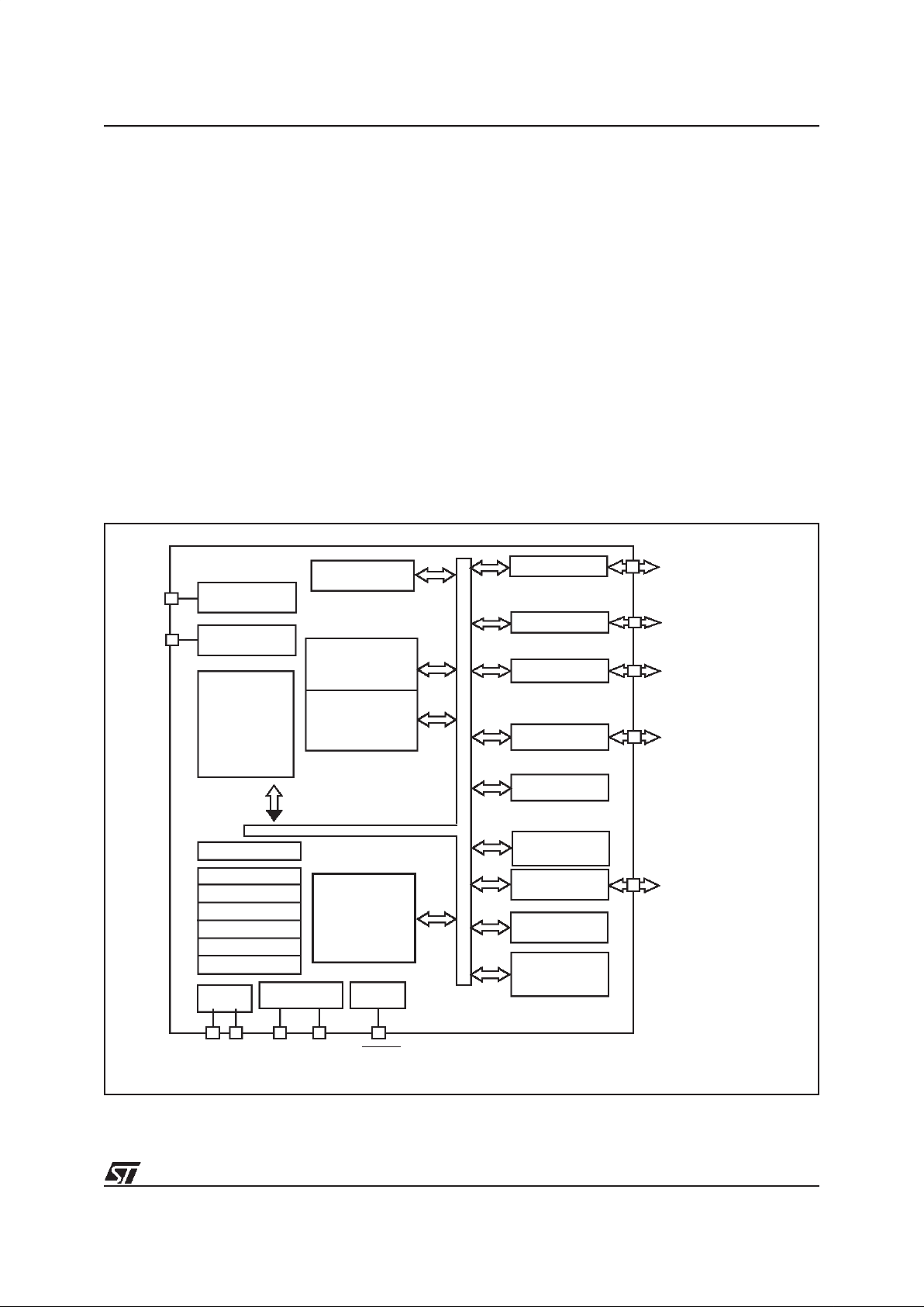
The ST62T28C and ST62E28C devices are low
cost members of the ST62xx 8-bit HCMOS family
of microcontrollers, which are targeted at low to
medium complexity applications. All ST62xx devices are based on a building block approach: a
common core is surrounded by a number of onchip peripherals.
The ST62E28C isthe erasableEPROM versionof
the ST62T28C device, which may be used to emulate theST62T28C device, as well as the respective ST6228C ROM devices.
OTP and EPROM devices are functionally identical. The ROM basedversions offer the same functionality selecting as ROM options the options de-
fined in the programmable option byte of the OTP/
EPROM versions.OTP devices offerall theadvantages of user programmability at low cost, which
make them the ideal choice in a wide range of applications where frequent code changes, multiple
code versions or last minute programmability are
required.
These compact low-cost devices feature a Timer
comprising an 8-bit counter and a 7-bit programmable prescaler, an 8-bit Auto-Reload Timer, with
1 input capture channel, capability, a serial asynchronous port interface (UART), a synchronous
serial port interface, an 8-bit A/D Converterwith 12
analog inputs and a Digital Watchdog timer, making them well suited for a wide range of automo-
Figure 1. Block Diagram
TEST
NMI
INTERRUPT
PROGRAM
PC
STACK LEVEL 1
STACK LEVEL 2
STACK LEVEL 3
STACK LEVEL 4
STACK LEVEL 5
STACK LEVEL 6
POWER
SUPPLY
OSCILLATOR
RESET
DATA ROM
USER
SELECTABLE
DATA RAM
PORT A
PORT B
TIMER
DIGITAL
8 BIT CORE
TEST/V
PP
8-BIT
A/D CONVERTER
V
DDVSS
OSCin OSCout RESET
WATCHDOG
Memory
PORT C
AUTORELOAD
TIMER
192 Bytes
7948 bytes
PB4..PB6/Ain
PC4..PC5/Ain
PORT D
PD6,PD7/Ain
PD1/Ain/Scl
PD2/Ain/Sin
PD3/Ain/Sout
PD4/Ain/RXD1
PD5/Ain/TXD1
(V
PP
on EPROM/OTP versionsonly)
TIMER
VR01823F
UART
PC6..PC7/20 mA Sink
SPI
PA0..PA1 / 20 mA Sink
PA2/ARTIMout / 20 mA Sink
PA3/ARTIMin/ 20 mA Sink
PA4..PA5/20 mASink
5
Page 6

6/84
ST62T28C/E28C
1.2 PIN DESCRIPTIONS
VDDand VSS. Power is supplied to the MCU via
these two pins. VDDis the power connection and
VSSis the ground connection.
OSCin and OSCout. These pins are internally
connected tothe on-chip oscillatorcircuit. A quartz
crystal, a ceramic resonator or an external clock
signal can be connected between these two pins.
The OSCin pin is the input pin, the OSCout pin is
the output pin.
RESET. The active-low RESET pin is used to restart themicrocontroller.
TEST/VPP. The TEST must be held at VSSfor nor-
mal operation. If TEST pin is connected to a
+12.5V level during the reset phase, the EPROM/
OTP programming Mode is entered.
NMI. TheNMI pinprovides the capability for asynchronous interruption,by applying anexternal non
maskable interrupt to the MCU. The NMI input is
falling edge sensitive with Schmitt trigger characteristics. The user can select as optionthe availability of an on-chip pull-up at this pin.
PA0-PA5. These 6 lines are organised as one I/O
port (A). Each line may be configured under software controlas inputs with or without internal pullup resistors, input with interrupt generation and
pull-up resistor, open-drain or push-pull outputs.
PA2/ARTIMout and PA3/ARTIMin can beused respectively as output and input pins for the embedded 8-bitAuto-Reload Timer.
In addition, PA0-PA5 can sink 20mAfor direct LED
or TRIAC drive.
PB4...PB6. These 3 lines areorganised asone I/O
port (B). Each line may be configured under software controlas inputs with or without internal pullup resistors, input with interrupt generation and
pull-up resistor, open-drain or push-pull outputs,
analog inputsfor the A/D converter.
PC4-PC7. These 4 lines are organised as one I/O
port (C). Each line may be configured under software control as input with or without internal pullup resistor, input with interrupt generation and
pull-up resistor, open-drain or push-pull output.
PC4 and PC5 can also beused as analog input for
the A/D converter, while PC6 and PC7 can sink
20mA for direct LED or TRIAC drive.
PD1...PD7. These7 lines are organised asoneI/O
port (portD). Each line may be configured under
software control as input with or without internal
pull-up resistor, input with interruptgeneration and
pull-up resistor, analog input open-drain or pushpull output. In addition, the pins PD5/TXD1 and
PD4/RXD1 can be used as UART output (PD5/
TXD1) or UARTinput (PD4/RXD1). Thepins PD3/
Sout, PD2/Sin and PD3/Scl can also be used respectively as data out, data in and clock pins for
the on-chip SPI.
TIMER.This is the TIMER 1 I/O pin. In input mode,
it is connected to the prescaler and acts as external timer clockor ascontrol gate for the internal
timer clock.In output mode, the TIMERpin outputs
the data bit when a time-out occurs.The user can
select as option the availability of an on-chip pullup at this pin.
Figure 2. ST62T28C/E28C Pin Configuration
1
2
3
4
5
6
7
8
9
10
11
12
13
14
15
16
17
18
19
20
V
DD
TIMER
OSCin
OSCout
NMI
TEST/V
PP
(1)
RESET
PC7*
PC6*
Ain/PC5
V
SS
PA0*
PA1*
PA2*/ARTIMout
PA3*/ARTIMin
PD3/Ain/Sout
PD4/Ain/RXD1
PD5/Ain/TXD1
PD6/Ain
PD7/Ain
28
27
26
25
24
23
22
21
Ain/PC4
Ain/PB6
Ain/PB5
Ain/PB4
PA4*
PA5*
PD1/Ain/Scl
PD2/Ain/Sin
(1) VPPon EPROM/OTP only
VR01804B
(*) 20 mA Sink
6
Page 7
7/84
ST62T28C/E28C
1.3 MEMORY MAP
1.3.1 Introduction
The MCU operates in three separate memory
spaces: Program space, Data space, and Stack
space. Operation in thesethree memory spacesis
described in the following paragraphs.
Briefly, Program space contains user program
code in Program memory and user vectors; Data
space contains user data in RAM and in Program
memory, andStack space accommodates six levels of stack for subroutine and interrupt service
routine nesting.
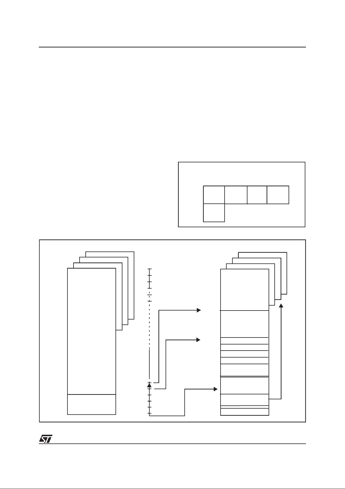
1.3.2 Program Space
Program Space comprises the instructions to be
executed, the data required for immediate addressing mode instructions, the reserved factory
test area and the user vectors. Program Space is
addressed viathe 12-bit ProgramCounter register
(PC register).
Program Space is organised in 4K pages. 4 of
them are addressed in the 000h-7FFh locations of
the Program Space by the Program Counter and
by writing the appropriate code in the Program
ROM Page Register (PRPR register). A common
(STATIC) 2K pageis available all the time for interrupt vectors and common subroutines, independently of the PRPR register content. This “STATIC”
page is directly addressed in the 0800h-0FFFh by
the MSB of the Program Counter register PC 11.
Note this page can also be addressed in the 0007FFh range. It is two different ways of addressing
the same physical memory.
Jump from a dynamic page to another dynamic
page is achieved by jumping back to the static
page, changing contents of PRPR and then jumping to the new dynamic page.
Figure 3. 8Kbytes Program SpaceAddressing
Figure 4. Memory Addressing Diagram
PC
SPACE
000h
7FFh
800h
FFFh
0000h
1FFFh
Page 0
Page 1
Static
Page
Page 2
Page 1
Static
Page
ROM SPACE
Page 3
PROGRAM SPACE
PROGRAM
INTERRUPT &
RESET VECTORS
ACCUMULATOR
DATA RAM
BANK SELECT
WINDOW SELECT
RAM
X REGISTER
Y REGISTER
V REGISTER
W REGISTER
DATA READ-ONLY
WINDOW
RAM / EEPROM
BANKING AREA
000h
03Fh
040h
07Fh
080h
081h
082h
083h
084h
0C0h
0FFh
0-63
DATA SPACE
0000h
0FF0h
0FFFh
MEMORY
MEMORY
DATA READ-ONLY
MEMORY
VR01568
7
Page 8

8/84
ST62T28C/E28C
MEMORY MAP(Cont’d)
Table 1. ST62E28C/T28C Program Memory Map
Note: OTP/EPROM devices can be programmed
with thedevelopment toolsavailable fromSTMicroelectronics (ST62E3X-EPB or ST623X-KIT).
1.3.2.1 Program ROM Page Register (PRPR)
The PRPR register can be addressed like a RAM
location in the Data Space at the address CAh;
nevertheless it is a write only register that cannot
be accessed with single-bit operations. Thisregister is used to select the 2-Kbyte ROM bank of the
Program Space that will be addressed. The
number ofthe page has to be loaded in the PRPR
register. Refer to the Program Space description
for additional information concerning the use of
this register. The PRPR register is not modified
when an interrupt or a subroutine occurs.
Care isrequired whenhandling the PRPR register
as it is write only. For this reason, it is not allowed
to change the PRPR contents while executing interrupt service routine, as the service routine
cannot save and then restore its previous content.
This operation may be necessary if common routines andinterrupt service routines take morethan
2K bytes; in this case it could be necessary to divide the interrupt service routineinto a (minor) part
in the static page (start and end) and to a second
(major) part in one of the dynamic pages. Ifit isimpossible to avoid the writing of this register ininterrupt service routines, an image of this register
must be saved in a RAM location, and each time
the program writes to the PRPR it must write also
to the image register. The image register must be
written before PRPR, so if an interrupt occurs between the two instructions the PRPR is not affected.
Program ROM Page Register (PRPR)
Address: CAh — Write Only
Bits 2-7= Not used.
Bit 5-0 = PRPR1-PRPR0:
Program ROM Select.
These two bits select the corresponding page to
be addressed in the lower part of the 4K program
address space as specified in Table 2.
This register is undefined on Reset. Neither read
nor single bit instructions may be used to address
this register.
Table 2. 6Kbytes Program ROM Page Register
Coding
1.3.2.2 Program Memory Protection
The Program Memory in OTP or EPROM devices
can be protected againstexternal readout of memory by selecting the READOUT PROTECTION option in the option byte.
In the EPROM parts, READOUT PROTECTION
option can be disactivated only by U.V. erasure
that also results into the whole EPROM context
erasure.
Note: Once the Readout Protectionis activated, it
is no longer possible, even for STMicroelectronics,
to gain access to the Program memory contents.
Returned parts with a protection set can therefore
not be accepted.
ROM Page Device Address Description
Page 0
0000h-007Fh
0080h-07FFh
Reserved
User ROM
Page 1
“STATIC”
0800h-0F9Fh
0FA0h-0FEFh
0FF0h-0FF7h
0FF8h-0FFBh
0FFCh-0FFDh
0FFEh-0FFFh
User ROM
Reserved
Interrupt Vectors
Reserved
NMI Vector
Reset Vector
Page 2
0000h-000Fh
0010h-07FFh
Reserved
User ROM
Page 3
0000h-000Fh
0010h-07FFh
Reserved
User ROM
70
- - - - - - PRPR1 PRPR0
PRPR1 PRPR0 PC bit 11 Memory Page
X X 1 Static Page (Page1)
0 0 0 Page 0
0 1 0 Page 1 (Static Page)
1 0 0 Page 2
1 1 0 Page 3
8
Page 9

9/84
ST62T28C/E28C
MEMORY MAP(Cont’d)
1.3.3 Data Space
Data Spaceaccommodates all the data necessary
for processingthe user program. This space comprises the RAM resource, the processor core and
peripheral registers, as well as read-only data
such as constants and look-up tables in Program
memory.
1.3.3.1 Data ROM
All read-only data is physically stored in program
memory, which also accommodates the Program
Space. The program memory consequently contains the program code to be executed, as well as
the constants and look-up tables required by the
application.
The Data Space locations in which the different
constants and look-up tables are addressed by the
processor core may be thought of as a 64-byte
window through which it is possible to access the
read-only data stored in Program memory.
1.3.3.2 Data RAM
In ST6228C and ST62E28C devices, the data
space includes 60 bytes of RAM, the accumulator
(A), the indirect registers (X), (Y), the short direct
registers (V), (W), the I/O port registers, the peripheral data and control registers, the interrupt
option register andthe Data ROM Window register
(DRW register).
Additional RAM pages can also be addressed using banks of 64 byteslocated between addresses
00h and3Fh.
1.3.4 Stack Space
Stack space consists of six 12-bit registers which
are used to stack subroutine and interrupt return
addresses, as wellas thecurrent program counter
contents.
Table 3. Additional RAM Banks
Table 4. ST62T28C/E28C Data Memory Space
Device RAM
ST62T28C/E28C 2 x 64bytes
DATA RAM BANKS
000h
03Fh
DATA ROM WINDOWAREA
040h
07Fh
X REGISTER 080h
Y REGISTER 081h
V REGISTER 082h
W REGISTER 083h
DATA RAM
084h
0BFh
PORT A DATAREGISTER 0C0h
PORT B DATAREGISTER 0C1h
PORT C DATAREGISTE R 0C2h
PORT D DATAREGISTE R 0C3h
PORT A DIRECTION REGISTER 0C4h
PORT B DIRECTION REGISTER 0C5h
PORT C DIRECTION REGISTE R 0C6h
PORT D DIRECTION REGISTE R 0C7h
INTERRUPT OPTION REGISTER 0C8h*
DATA ROM WINDOW REGISTER 0C9h*
ROM BANK SELECT REGISTER 0CAh*
RAM BANK SELECT REGISTER 0CBh*
PORT A OPTION REGISTER 0CCh
PORT B OPTION REGISTER 0CDh
PORT C OPTION REGISTER 0CEh
PORT D OPTION REGISTER 0CFh
A/D DATA REGISTER 0D0h
A/D CONTROL REGISTER 0D1h
TIMER 1 PRESCALER REGISTER 0D2h
TIMER 1 COUNTERREGISTER 0D3h
TIMER 1 STATUS/CONTROL REGISTER 0D4h
RESERVED 0D5h
UARTDATA SHIFT REGISTER 0D6h
UARTSTATUS CONTROL REGISTER 0D7h
WATCHDOGREGISTER 0D8h
RESERVED 0D9h
I/O INTERRUPT POLARITY REGISTER 0DAh
SPI INTERRUPT DISABLE REGISTER 0DCh*
SPI DATASHIFT REGISTER 0DDh
RESERVED
0DEh
0E4h
ARTIMER MODE/CONTROL REGISTER 0E5h
ARTIMER STATUS/CONTROLREGISTER ARSC0 0E6h
ARTIMER STATUS/CONTROLREGISTER ARSC1 0E7h
RESERVED 0E8h
ARTIMER RELOAD/CAPTURE REGISTER 0E9h
ARTIMER COMPARE REGISTER 0EAh
. ARTIMER LOAD REGISTER 0EBh
RESERVED 0ECh
ACCUMULATOR OFFh
* WRITE ONLYREGISTER
9
Page 10
10/84
ST62T28C/E28C
MEMORY MAP(Cont’d)
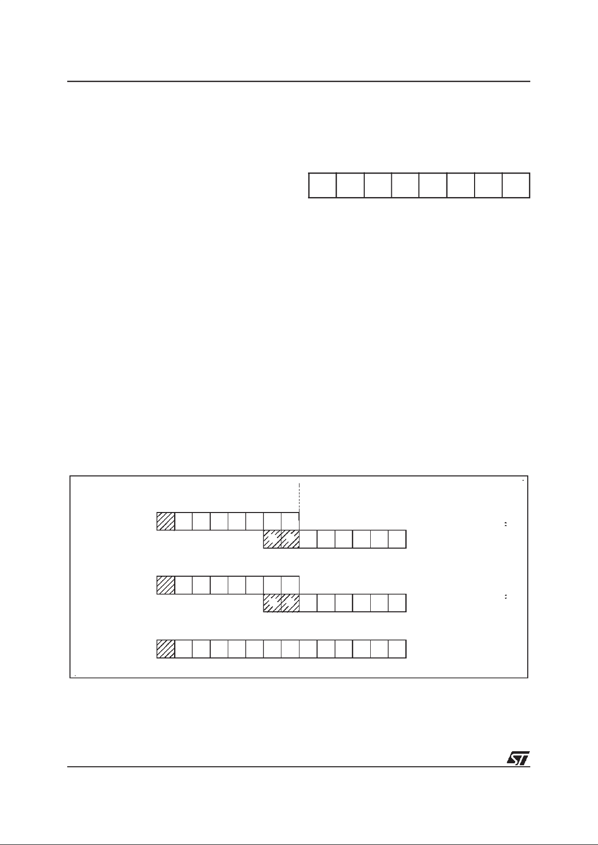
1.3.5 Data Window Register (DWR)
TheData read-only memorywindowislocatedfrom
address 0040h toaddress 007Fh in Data space. It
allows directreading of 64consecutive bytes located anywhere in program memory, between address 0000h and 1FFFh (top memory address depends on the specific device). All the program
memory can therefore be used to store either instructions or read-only data. Indeed, the window
can be moved in steps of 64 bytes along the program memorybywriting theappropriatecode inthe
Data Window Register (DWR).
The DWR can beaddressed like any RAMlocation
in theData Space,it is however a write-only register andtherefore cannotbe accessed using singlebit operations. This register is used to position the
64-byte read-onlydata window (from address 40h
to address 7Fh of the Data space) in program
memory in 64-byte steps. The effective address of
the byte to be read as data in program memory is
obtained by concatenating the 6 least significant
bits of the registeraddress given in the instruction
(as least significant bits) and the content of the
DWR register (asmost significant bits), as illustrated in Figure 5 below. For instance, when addressing location 0040h of the Data Space, with 00h
loaded in the DWR register, the physical location
addressed in program memory is 00h. The DWR
register is not cleared on reset, therefore it must
be written to prior to the first access to the Data
read-only memory window area.
Data Window Register (DWR)
Address: 0C9h — Write Only
Bits 7 = Not used.
Bit 6-0 = DWR6-DWR0:
Data read-only memory
Window Register Bits.
These are the Data readonly memory Window bits that correspond to the
upper bits of the dataread-only memory space.
Caution:
This register is undefined on reset. Neither read nor single bit instructionsmay beused to
address this register.
Note: Care is required when handling the DWR
register as it is write only. For this reason, the
DWR contents should not be changed while executing an interrupt service routine, as the service
routine cannot saveand then restore the register’s
previous contents. If it is impossible to avoid writing to the DWRduring the interrupt service routine,
an image of the register must be saved in a RAM
location, and each time the program writes to the
DWR, it must also writeto the image register. The
image register must be written first so that, if aninterrupt occurs between the two instructions, the
DWR is not affected.
Figure 5. Data read-only memory Window Memory Addressing
70
- DWR6 DWR5 DWR4 DWR3 DWR2 DWR1 DWR0
DATA ROM
WINDOW REGISTER
CONTENTS
DATA SPACE ADDRESS
40h-7Fh
IN INSTRUCTION
PROGRAM SPACE ADDRESS
765432 0
543210
543210
READ
1
67891011
01
VR01573A
12
1
0
DATA SPACE ADDRESS
59h
0000
01001
11
Example:
(DWR)
DWR=28h
11
00000000
1
ROM
ADDRESS:A19h
11
13
0
1
10
Page 11

11/84
ST62T28C/E28C
MEMORY MAP(Cont’d)
1.3.6 Data RAM Bank Register (DRBR)
Address: CBh — Write only
Bit 7-5= These bits are not used
Bit 4 - DRBR4. This bit, when set, selects RAM
Page 2.
Bit 3 - DRBR3. This bit, when set, selects RAM
Page 1.
Bit 2.0 These bits are not used.
The selection of the bank is madeby programming
the Data RAM Bank Switch register (DRBR register) located at address CBh of the Data Space according to Table 1.No more than onebank should
be set at a time.
The DRBR register can be addressed like a RAM
Data Space location at the address CBh; nevertheless itis awrite only register that cannot be accessed with single-bit operations. This register is
used to select the desired 64-byte RAM bank of
the Data Space. The number of banks has to be
loaded in the DRBR register and the instruction
has to point to the selected location as if it was in
bank 0 (from 00h address to 3Fh address).
This registeris not cleared during the MCU initialization, therefore it must be written before the first
access to the Data Space bank region. Refer to
the Data Space description for additional information. The DRBR register is not modified when an
interrupt or a subroutine occurs.
Notes:
Care is requiredwhen handling the DRBR register
as it is write only. For this reason, it is not allowed
to change the DRBR contents while executing interrupt service routine, as the service routine cannot save and then restore its previous content. If it
is impossible to avoid the writing of this register in
interrupt service routine, an image of this register
must be saved in a RAM location, and each time
the program writes to DRBR it must write also to
the image register. The image register must be
written first, so if an interrupt occurs between the
two instructions the DRBR is not affected.
In DRBR Register, only 1 bit must be set. Otherwise two or more pages are enabled in parallel,
producing errors.
Table 5. Data RAM Bank Register Set-up
70
- - - DRBR4 DRBR3 - - -
DRBR ST62T28C/E28C
00h None
01h Reserved
02h Reserved
08h RAM Page 1
10h RAM Page 2
other Reserved
11
Page 12

12/84
ST62T28C/E28C
1.4 PROGRAMMING MODES
1.4.1 Option Bytes
The two Option Bytes allow configurationcapability to the MCUs. Option byte’s content is automatically read, and the selected options enabled,when
the chipreset is activated.
It can only be accessed during the programming
mode. This access is made either automatically
(copy from a master device) or by selecting the
OPTION BYTE PROGRAMMING modeof the programmer.
The option bytes are located in a non-user map.
No address has to bespecified.
EPROM Code Option Byte (LSB)
EPROM Code Option Byte (MSB)
D15-D13. Reserved. Must be cleared.
ADC SYNCHRO. When set, an A/D conversion is
started upon WAIT instruction execution, in order
to reduce supply noise.When this bit is low, an A/
D conversion is started as soon as the STA bit of
the A/D Converter Control Registeris set.
D11.
UART Frame.
When set, UARTtransmission
and reception are based on a 11-bit frame. When
cleared, a 10-bit frame isused.
D10. Reserved
.
EXTCNTL.
External STOP MODE control.
. When
EXTCNTL is high, STOP mode is available with
watchdog active by setting NMI pin to one. When
EXTCNTL is low, STOP mode is not available with
the watchdog active.
LVD.
LVDRESET enable.
When this bit is set, safe
RESET is performed by MCU when the supply
voltage is too low. When this bit is cleared, only
power-on reset or external RESETare active.
PROTECT.
Readout Protection.
This bitallows the
protection of the software contents against piracy.
When the bit PROTECT is set high, readout of the
OTP contents is prevented by hardware.. When
this bit is low, the user program can be read.
OSCIL.
Oscillator selection
. When this bit is low,
the oscillator must be controlled by a quartz crystal, a ceramic resonator or an external frequency.
When it is high, the oscillator must be controlled by
an RC network, with only the resistor having to be
externally provided.
D5.
Port Pull.
This bit must be set high to disable
pull-up at reset on the I/O port. When this bit is
low,I/O ports are in input with pull-up.
D4. Reserved. Must be clearedto zero.
NMI PULL.
NMI Pull-Up
. This bit must be set high
to configure the NMI pin with a pull-up resistor.
When it is low, no pull-up is provided.
TIM PULL.
TIM Pull-Up
. This bit must be set high
to configure the TIMER pin with a pull-up resistor.
When it is low, no pull-up is provided.
WDACT. This bit controls the watchdog activation.
When it is high, hardware activation is selected.
The software activation is selected when WDACT
is low.
OSGEN.
Oscillator Safe Guard
. This bit must be
set high to enable the Oscillator Safe Guard.
When this bit is low, the OSG is disabled.
The Option byte is written during programming either by using the PC menu (PC driven Mode) or
automatically (stand-alone mode).
70
PROTECT
OSCIL
PORT
PULL
-
NMI
PULL
TIM
PULL
WDACT
OS-
GEN
15 8
---
ADC
SYNCHRO
UART
FRAME
-
EXTC-
NTL
LVD
12
Page 13
13/84
ST62T28C/E28C
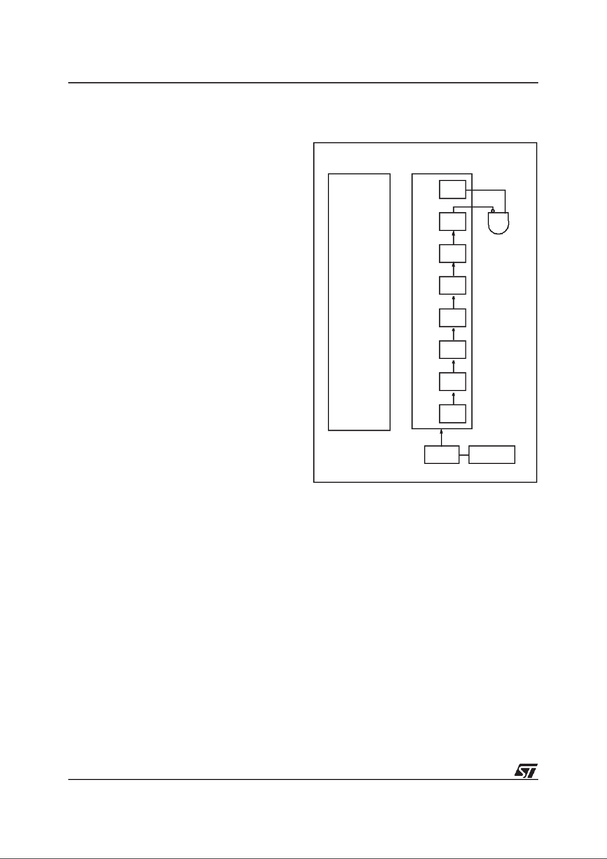
2 CENTRAL PROCESSING UNIT
2.1 INTRODUCTION
The CPUCoreof ST6 devicesis independentofthe
I/O or Memory configuration. As such, it may be
thought of as an independent central processor
communicating with on-chip I/O, Memory and Peripherals via internal address, data, and control
buses. In-core communication is arranged as
shown in Figure 6; the controller being externally
linked to both the Reset and Oscillator circuits,
while thecore is linkedto thededicated on-chip peripherals via the serial data bus and indirectly, for
interrupt purposes, through the control registers.
2.2 CPU REGISTERS
TheST6FamilyCPUcorefeaturessixregisters and
three pairs of flags available to the programmer.
These are described in the following paragraphs.
Accumulator (A). The accumulator is an 8-bit
general purpose register used in all arithmetic calculations, logical operations, and data manipulations. The accumulator can be addressed in Data
space as a RAM location at address FFh. Thus the
ST6 can manipulate the accumulator just like any
other register in Data space.
Indirect Registers (X, Y). These two indirect registers are used as pointers to memory locations in
Data space. They are used in the register-indirect
addressing mode. These registers can be addressed in the data space as RAM locations at addresses 80h (X) and 81h (Y). They canalso be accessed with the direct, shortdirect, orbit direct addressing modes. Accordingly, the ST6 instruction
set can usethe indirect registers as any other register of the data space.
Short Direct Registers (V, W). These two registers are used to save a byte in short direct addressing mode. They can be addressed in Data
space as RAM locationsat addresses 82h (V) and
83h (W). They can also be accessed using the direct and bit direct addressing modes. Thus, the
ST6 instruction set can use the short direct registers as any other register of the data space.
Program Counter (PC). The program counter is a
12-bit register which contains the address of the
next ROM location to be processed by the core.
This ROM location may be an opcode, an operand, or the address of an operand. The 12-bit
length allows the direct addressing of 4096 bytes
in Program space.
Figure 6. ST6 Core Block Diagram
PROGRAM
RESET
OPCODE
FLAG
VALUES
2
CONTROLLER
FLAGS
ALU
A-DATA
B-DATA
ADDRESS/READ LINE
DATA SPACE
INTERRUPTS
DATA
RAM/EEPROM
DATA
ROM/EPROM
RESULTS TO DATA SPACE (WRITE LINE)
ROM/EPROM
DEDICATIONS
ACCUMULATOR
CONTROL
SIGNALS
OSCin
OSCout
ADDRESS
DECODER
256
12
Program Counter
and
6 LAYER STACK
0,01 TO 8MHz
VR01811
13
Page 14
14/84
ST62T28C/E28C
CPU REGISTERS (Cont’d)
However, if theprogram space contains morethan
4096 bytes, the additional memory in program
space can be addressed by using the Program
Bank Switch register.
The PC value is incremented after reading the address of the current instruction. To execute relative
jumps, the PC and the offset are shifted through
the ALU, where they are added; the result is then
shifted back into the PC.The program counter can
be changed in the following ways:
- JP (Jump) instructionPC=Jump address
- CALL instructionPC= Call address
- Relative Branch Instruction.PC= PC +/- offset
- Interrupt PC=Interrupt vector
- Reset PC= Reset vector
- RET & RETIinstructionsPC= Pop (stack)
- Normal instructionPC= PC + 1
Flags (C, Z). TheST6 CPU includes three pairs of
flags (Carryand Zero), eachpair beingassociated
with one of the three normal modes of operation:
Normal mode, Interrupt mode and Non Maskable
Interrupt mode. Each pair consists of a CARRY
flag and a ZERO flag. One pair (CN, ZN) is used
during Normal operation,another pair is usedduring Interrupt mode (CI, ZI), anda third pair is used
in the Non Maskable Interrupt mode (CNMI, ZNMI).
The ST6 CPU uses the pair of flags associated
with the current mode: as soon as an interrupt (or
a Non Maskable Interrupt) is generated, the ST6
CPU uses the Interrupt flags (resp. the NMI flags)
instead of the Normal flags. When the RETI instruction is executed, the previously used set of
flags is restored. It should be noted that each flag
set can only be addressed in its own context (Non
Maskable Interrupt, Normal Interrupt or Main routine). The flags are not cleared during context
switching andthus retain their status.
The Carry flag is set when a carry or a borrow occurs during arithmetic operations; otherwise it is
cleared. The Carry flag is also set to the value of
the bit tested in a bit test instruction;it also participates inthe rotate left instruction.
The Zero flag isset ifthe result of the lastarithmetic or logical operation was equal to zero; otherwise itis cleared.
Switching between the three sets of flags is performed automatically when an NMI, an interruptor
a RETI instructions occurs. As the NMI mode is
automatically selected after the reset of the MCU,
the ST6 core uses at first the NMI flags.
Stack. The ST6 CPU includes a true LIFO hardware stack which eliminates the need for a stack
pointer. The stack consists of six separate 12-bit
RAM locations that do not belong to the data
space RAM area. When asubroutine call (or interrupt request)occurs, the contents of each level are
shifted into the next higher level, while the content
of the PC is shifted into the first level (the original
contents of the sixth stack level are lost). When a
subroutine or interrupt return occurs (RET or RETI
instructions), the first level register is shifted back
into the PC and the value of each level is popped
back into the previous level. Since the accumulator, in common with all other data space registers,
is not stored in this stack, management of these
registers should be performed within the subroutine. The stack will remain in its “deepest” position
if morethan 6 nested calls orinterrupts are executed, and consequently the last return address will
be lost. It will also remain in its highest position if
the stack is empty and a RET orRETI is executed.
In this case the nextinstruction will be executed.
Figure 7. ST6 CPU Programming Mode
l
SHORT
DIRECT
ADDRESSING
MODE
VREGISTER
W REGISTER
PROGRAMCOUNTER
SIX LEVELS
STACKREGISTER
CZNORMAL FLAGS
INTERRUPTFLAGS
NMI FLAGS
INDEX
REGISTER
VA000 4 23
b7
b7
b7
b7
b7
b0
b0
b0
b0
b0
b0b11
ACCUM ULATOR
Y REG. POINTER
X REG. POINTER
CZ
CZ
14
Page 15

15/84
ST62T28C/E28C
3 CLOCKS, RESET, INTERRUPTS AND POWER SAVING MODES
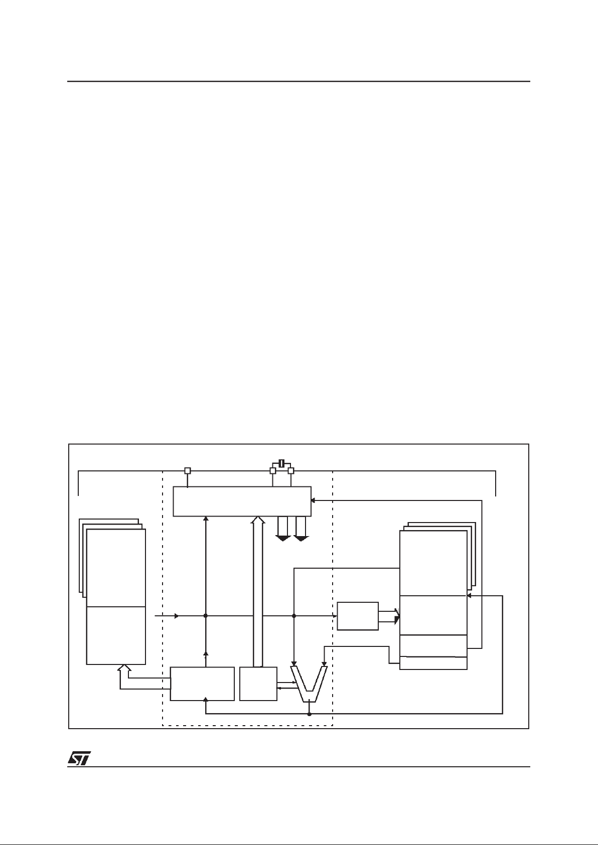
3.1 CLOCK SYSTEM
The MCU features a Main Oscillatorwhich can be
driven byan external clock, or used in conjunction
with an AT-cut parallel resonant crystal or a suitable ceramic resonator, or with an external resistor
(R
NET
). In addition, a Low FrequencyAuxiliary Oscillator (LFAO)can be switched in for security reasons, to reduce powerconsumption, orto offerthe
benefits of a back-up clock system.
The Oscillator Safeguard (OSG) option filters
spikes from the oscillator lines, provides access to
the LFAO to provide a backup oscillator in the
event of main oscillator failure and also automatically limits the internal clock frequency (f
INT
)asa
function of VDD, inorder toguarantee correct operation. These functions are illustrated in Figure 2,
Figure 3, Figure 4 and Figure 5.
Figure 1 illustrates various possible oscillator configurations using anexternal crystal or ceramicresonator, an external clock input, anexternal resistor
(R
NET
), or the lowest cost solution using only the
LFAO. CL1anCL2shouldhave acapacitance in the
range 12 tST6_CLK1o 22 pF for an oscillator frequency in the 4-8 MHz range.
The internal MCU clock frequency (f
INT
) is divided
by 12to drive the Timer, the A/D converter and the
Watchdog timer, and by 13 to drive the CPU core,
as may be seen in Figure 4.
With an 8MHz oscillator frequency, the fastest machine cycle is therefore 1.625µs.
A machine cycleis the smallest unit of time needed
to executeanyoperation(for instance,toincrement
the Program Counter). An instruction may require
two, four, or five machine cycles forexecution.
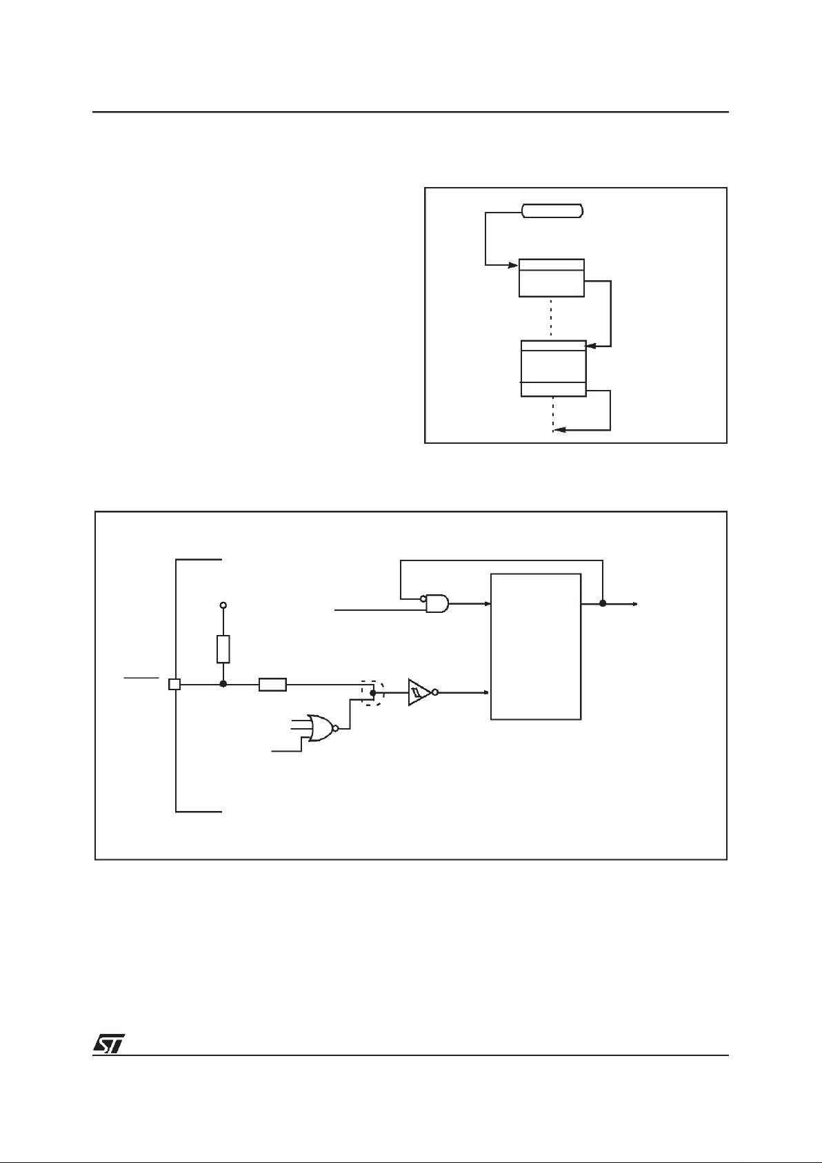
3.1.1 Main Oscillator
The oscillatorconfigurationmay bespecified byselectingtheappropriate option.When theCRYSTAL/
RESONATORoptionisselected,itmustbeusedwith
a quartz crystal,a ceramic resonator oran external
signalprovidedontheOSCinpin.WhentheRCNETWORK option isselected, thesystem clock is generated by an external resistor.
The main oscillator can be turned off (when the
OSG ENABLED option isselected) by setting the
OSCOFF bit of the ADC Control Register. The
Low Frequency Auxiliary Oscillator isautomatically started.
Figure 8. Oscillator Configurations
INTEGRATED CLOCK
CRYSTAL/RESONATOR option
OSG ENABLED option
OSC
in
OSC
out
C
L1n
C
L2
ST6xxx
CRYSTAL/RESONATOR CLOCK
CRYSTAL/RESONATOR option
OSC
in
OSC
out
ST6xxx
EXTERNAL CLOCK
CRYSTAL/RESONATOR option
NC
OSC
in
OSC
out
ST6xxx
NC
OSC
in
OSC
out
R
NET
ST6xxx
RC NETWORK
RC NETWORK option
NC
15
Page 16

16/84
ST62T28C/E28C
CLOCK SYSTEM (Cont’d)
Turning on the main oscillator is achieved by resetting the OSCOFF bit of the A/DConverter Control Register or by resetting the MCU. Restarting
the main oscillator implies a delay comprising the
oscillator start up delay period plus the duration of
the softwareinstruction at f
LFAO
clock frequency.
3.1.2 Low Frequency Auxiliary Oscillator
(LFAO)
The Low Frequency Auxiliary Oscillator has three
main purposes. Firstly, it can be used to reduce
power consumption in non timing critical routines.
Secondly, it offers a fully integrated system clock,
without anyexternal components.Lastly, itacts as
a safetyoscillator in caseof main oscillator failure.
This oscillator is available when the OSG ENABLED option is selected. In this case, it automatically startsone of its periods after the first missing
edge from the main oscillator, whatever the reason
(main oscillatordefective, no clock circuitry provided, main oscillator switched off...).
User code,normal interrupts, WAIT and STOP instructions, are processed as normal, at the reduced f
LFAO
frequency.The A/D converter accuracy is decreased, since the internal frequency is below 1MHz.
At power on, the Low Frequency Auxiliary Oscillator starts faster than the Main Oscillator. It therefore feeds the on-chip counter generating the POR
delay untilthe Main Oscillator runs.
The Low Frequency Auxiliary Oscillator is automatically switched off as soon as the main oscillator starts.
ADCR
Address: 0D1h — Read/Write
Bit 7-3, 1-0= ADCR7-ADCR3, ADCR1-ADCR0:
ADC ControlRegister
. These bits are not used.
Bit 2 = OSCOFF. When low, this bit enables main
oscillator torun. The mainoscillator isswitched off
when OSCOFF is high.
3.1.3 Oscillator Safe Guard
The Oscillator Safe Guard (OSG) affordsdrastically increasedoperational integrity in ST62xx devices. The OSG circuit provides three basic func-
tions: it filtersspikes from theoscillator lines which
would result inover frequency to the ST62 CPU; it
gives access to the Low Frequency Auxiliary Oscillator (LFAO), used to ensure minimum processing in case of main oscillator failure, to offer reduced power consumptionor to provide afixed frequency low cost oscillator; finally, it automatically
limits the internal clock frequency as a function of
supply voltage, in order to ensure correct operation even if the power supply should drop.
The OSG is enabled or disabled by choosing the
relevant OSG option. It may be viewed as a filter
whose cross-over frequency is device dependent.
Spikes on the oscillatorlines result in an effectively
increased internal clock frequency.In the absence
of an OSG circuit, this may lead to an over frequency for a given power supply voltage. The
OSG filters out such spikes (as illustrated in Figure
2). In all cases, when the OSG isactive, the maximum internal clock frequency, f
INT
, is limited to
f
OSG
, which is supply voltage dependent. This re-
lationship is illustrated in Figure 5.
When the OSG is enabled, the Low Frequency
Auxiliary Oscillator maybe accessed. This oscillator starts operating after the first missing edge of
the main oscillator (see Figure 3).
Over-frequency, at a given power supply level, is
seen by the OSG as spikes; it therefore filters out
some cycles in order that the internal clock frequency of the device is kept within the range the
particular device can stand (depending on VDD),
and below f
OSG
: the maximum authorised frequen-
cy with OSG enabled.
Note. The OSGshould be used wherever possible
as it provides maximumsafety. Care must be taken, however, as it can increase power consumption and reduce the maximum operating frequency
to f
OSG
.
Warning: Care has to be taken when using the
OSG, as the internal frequency is defined between
a minimum and amaximum value and is not accurate.
For precise timing measurements, it is not recommended to use the OSG and it should not be enabled in applications that use the SPI or the UART.
It should also be noted that power consumption in
Stop mode is higher when the OSG is enabled
(around 50µA at nominal conditions and room
temperature).
70
ADCR7ADCR6ADCR5ADCR4ADCR3OSC
OFF
ADCR1ADCR
0
16
Page 17
17/84
ST62T28C/E28C
CLOCK SYSTEM (Cont’d)
Figure 9. OSG Filtering Principle
Figure 10. OSG Emergency Oscillator Principle
(1)
VR001932
(3)
(2)
(4)
(1)
(2)
(3)
(4)
Maximum Frequency for the device to work correctly
Actual Quartz Crystal Frequency at OSCin pin
Noise from OSCin
Resulting Internal Frequency
Main
VR001933
Internal
Emergency
Oscillator
Frequency
Oscillator
17
Page 18

18/84
ST62T28C/E28C
CLOCK SYSTEM (Cont’d)
Figure 11. Clock Circuit Block Diagram
Figure 12. Maximum Operating Frequency (f
MAX
) versus Supply Voltage (VDD)
Notes:
1. In this area, operation is guaranteed at the
quartz crystal frequency.
2. When the OSG is disabled, operation in this
area isguaranteed at the crystal frequency. When
the OSGis enabled, operation in this area isguaranteed at a frequency of at least f
OSG Min.
3. When the OSG is disabled, operation in this
area is guaranteed at the quartz crystalfrequency.
When the OSG is enabled, access to this area is
prevented. The internal frequency is kept a f
OSG.
4. When the OSG is disabled, operation in this
area is not guaranteed
When the OSG is enabled, access to this area is
prevented. The internal frequency is kept at f
OSG.
MAIN
OSCILLATOR
OSG
LFAO
M
U
X
Core
:13
:12
:1
TIMER 1
Watchdog
POR
f
INT
Main Oscillator off
1
2.5 3.6 4 4.5 5 5.5 6
8
7
6
5
4
3
2
Maximum FREQUENCY (MHz)
SUPPLY VOLTAGE (V
DD
)
FUNCTIONALITY IS NOT
3
4
3
2
1
f
OSG
f
OSG
Min (at 85°C)
GUARANTEED
IN THIS AREA
VR01807J
f
OSG
Min (at 125°C)
18
Page 19
19/84
ST62T28C/E28C
3.2 RESETS
The MCU can be reset in four ways:
– by the external Reset input being pulled low;
– by Power-onReset;
– by the digital Watchdog peripheral timing out.
– by LowVoltage Detection (LVD)
3.2.1 RESET Input
The RESET pin may be connected to a device of
the application board in order to reset the MCU if
required. The RESET pin may be pulled low in
RUN, WAIT or STOP mode. This input can be
used toreset the MCU internal state and ensure a
correct start-up procedure. The pin is active low
and features a Schmitt trigger input. The internal
Reset signal is generated by adding a delay to the
external signal. Therefore even short pulses on
the RESET pin are acceptable, provided VDDhas
completed its rising phase and that the oscillator is
running correctly (normal RUN or WAIT modes).
The MCU is keptin the Reset state as long as the
RESET pin is held low.
If RESET activation occurs in the RUN or WAIT
modes, processing of the user program is stopped
(RUN modeonly), the Inputs and Outputs are configured as inputs with pull-up resistors and the
main Oscillator is restarted. When the level on the
RESET pin then goes high, the initialization sequence is executed following expiry of the internal
delay period.
If RESET pinactivation occurs in the STOP mode,
the oscillator starts up and all Inputs and Outputs
are configured as inputs with pull-up resistors.
When the level of the RESET pin then goes high,
the initialization sequence is executed following
expiry of the internal delay period.
3.2.2 Power-on Reset
The function of the POR circuit consists in waking
up the MCU by detecting around 2V a dynamic
(rising edge) variation of the VDD Supply. At the
beginning of this sequence, the MCU is configured
in the Reset state: all I/O ports are configured as
inputs with pull-up resistors and no instruction is
executed. When the power supply voltage rises to
a sufficient level, the oscillator starts to operate,
whereupon aninternal delayis initiated, inorder to
allow the oscillator to fully stabilize before executing the first instruction. The initialization sequence
is executed immediately following the internal delay.
To ensure correct start-up, the user should take
care that the VDD Supply is stabilized at a sufficient level for the chosen frequency (see recommended operation) before the reset signal is released. In addition, supply rising must start from
0V.
As a consequence, the POR does not allow to supervise static, slowly rising, or falling, or noisy
(presenting oscillation) VDD supplies.
An external RC network connected to the RESET
pin, or the LVD reset can be used instead to get
the best performances.
Figure 13. Reset and Interrupt Processing
INT LATCH CLEARED
NMI MASK SET
RESET
( IF PRESENT )
SELECT
NMI MODE FLAGS
IS RESET STILL
PRESENT?
YES
PUT FFEH
ON ADDRESS BUS
FROM RESET LOCATIONS
FFE/FFF
NO
FETCH INSTRUCTION
LOAD PC
VA000427
19
Page 20
20/84
ST62T28C/E28C
RESETS (Cont’d)
3.2.3 Watchdog Reset
The MCU provides a Watchdog timer function in
order to ensure graceful recovery from software
upsets. If the Watchdog register is not refreshed
before an end-of-count condition is reached, the
internal reset will be activated. This, amongst other things, resets the watchdog counter.
The MCU restarts just as though the Reset had
been generated by the RESET pin, including the
built-in stabilisation delay period.
3.2.4 LVD Reset
The on-chip Low Voltage Detector, selectable as
user option, features static Reset when supply
voltage is below a reference value. Thanks to this
feature, external reset circuit can be removed
while keeping the application safety. This SAFE
RESET is effective as well in Power-on phase as
in power supply drop with different reference val-
ues, allowing hysteresiseffect. Referencevalue in
case of voltage drop has been set lower than the
reference value for power-on in order to avoid any
parasitic Reset when MCU start’s running and
sinking current on the supply.
As long as the supply voltage is below the reference value, there is a internal and static RESET
command. The MCU can start only when the supply voltage rises over the reference value. Therefore, only two operating mode exist for the MCU:
RESET active below the voltage reference, and
running mode over the voltage reference as
shown on the Figure 14, that represents a powerup, power-down sequence.
Note: When the RESET state is controlled by one
of the internal RESET sources (Low Voltage Detector, Watchdog, Power on Reset), the RESET
pin is tied to low logiclevel.
Figure 14. LVD Reset on Power-on and Power-down (Brown-out)
3.2.5 Application Notes
No external resistor is required between VDDand
the Reset pin, thanks to the built-in pull-up device.
Direct external connection of the pin RESET to
VDDmust be avoided in order to ensure safe behaviour of the internal reset sources (AND.Wired
structure).
RESET
RESET
VR02106A
time
V
Up
V
dn
V
DD
20
Page 21
21/84
ST62T28C/E28C
RESETS (Cont’d)
3.2.6 MCU Initialization Sequence
When a reset occurs the stack is reset, the PC is
loaded with the address of the Reset Vector (located in programROM starting at address 0FFEh). A
jump tothe beginning of the user program must be
coded at this address. Following a Reset, the Interrupt flag is automatically set, so that the CPU is
in NonMaskable Interrupt mode; thisprevents the
initialisation routinefrom being interrupted. The initialisation routine should therefore be terminated
by a RETI instruction, in order to revert to normal
mode and enable interrupts. Ifno pending interrupt
is present at theend of the initialisation routine, the
MCU will continue by processing the instruction
immediately following the RETIinstruction. If, however, a pending interrupt is present, it will be serviced.
Figure 15. Reset and Interrupt Processing
Figure 16. Reset Block Diagram
RESET
RESET
VECTOR
JP
JP:2 BYTES/4 CYCLES
RETI
RETI: 1 BYTE/2 CYCLES
INITIALIZATION
ROUTINE
VA00181
V
DD
RESET
R
PU
R
ESD
1)
POWER
WATCHDOG RESET
CK
COUNTER
RESET
ST6
INTERNAL
RESET
f
OSC
RESET
ON RESET
LVD RESET
VR02107A
AND. Wired
1) Resistive ESD protection. Value not guaranteed.
21
Page 22

22/84
ST62T28C/E28C
RESETS (Cont’d)
Table 6. Register Reset Status
Register Address(es) Status Comment
Port Data Registers
Port Direction Register
Port Option Register
Interrupt Option Register
TIMER Status/Control
AR TIMER Mode/Control Register
AR TIMER Status/Control Register 0
AR TIMER Status/Control Register 1
0C0h to0C3h
0C4h to0C7h
0CCh to 0CFh
0C8h
0D4h
0E5h
0E6h
0E7h
00h
I/O are Input with or without pull-up
depending on PORT PULL option
Interrupt disabled
TIMER disabled
AR TIMER disabled
X, Y,V,W, Register
Accumulator
Data RAM
Data RAM Page Register
Data ROMWindow Register
A/D Result Register
ARTIMER Reload/Capture Register
ARTIMER Compare Registers
ARTIMER Load Registers
080H TO083H
0FFh
084h to 0BFh
0CBh
0C9h
0D0h
0E9h
0EAh
0EBh
Undefined
TIMER Counter Register
TIMER Prescaler Register
Watchdog Counter Register
A/D Control Register
0D3h
0D2h
0D8h
0D1h
FFh
7Fh
FEh
40h
Max count loaded
A/D in Stand-by
UART Status Control 0D7h UARTdisabled
22
Page 23

23/84
ST62T28C/E28C
3.3 DIGITAL WATCHDOG
The digital Watchdog consists of a reloadable
downcounter timer which can be used to provide
controlled recoveryfrom software upsets.
The Watchdog circuitgenerates a Reset when the
downcounter reaches zero. User software can
prevent this reset by reloading the counter, and
should therefore be written so that the counter is
regularly reloaded while the user program runs
correctly. Inthe eventof a software mishap (usually caused by externally generated interference),
the userprogram will no longerbehave in its usual
fashion and the timer register will thus not be reloaded periodically. Consequently the timer will
decrement down to 00h and reset the MCU. In order to maximise the effectiveness of the Watchdog
function, user software must be written with this
concept in mind.
Watchdog behaviour is governed by two options,
known as “WATCHDOG ACTIVATION” (i.e.
HARDWARE or SOFTWARE) and “EXTERNAL
STOP MODE CONTROL” (see Table7).
In the SOFTWARE option, the Watchdog is disabled until bit Cof the DWDR registerhas been set.
When the Watchdog is disabled, low power Stop
mode is available. Once activated, the Watchdog
cannot be disabled, except by resetting the MCU.
In the HARDWARE option, the Watchdog is permanently enabled. Sincethe oscillator willrun continuously, low power mode is not available. The
STOP instruction is interpreted as a WAIT instruction, and the Watchdog continues to countdown.
However, when the EXTERNAL STOP MODE
CONTROL option has been selected low power
consumption may be achieved in Stop Mode.
Execution of the STOP instruction is then governed by a secondary function associated with the
NMI pin. If a STOP instruction is encountered
when the NMI pin is low, it is interpreted as WAIT,
as described above. If, however, the STOP instruction is encountered when the NMIpin is high,
the Watchdog counter is frozen and the CPU enters STOP mode.
When the MCU exits STOPmode (i.e. when aninterrupt is generated), the Watchdog resumes its
activity.
Table 7. Recommended Option Choices
Functions Required Recommended Options
Stop Mode & Watchdog “EXTERNAL STOP MODE” &“HARDWARE WATCHDOG”
Stop Mode “SOFTWARE WATCHDOG”
Watchdog “HARDWARE WATCHDOG”
23
Page 24
24/84
ST62T28C/E28C
DIGITAL WATCHDOG (Cont’d)
The Watchdog is associated with a Data space
register (Digital WatchDog Register, DWDR, location 0D8h) which is described in greater detail in
Section 3.3.1Digital Watchdog Register (DWDR).
This register is set to 0FEh on Reset: bit C is
cleared to “0”, which disables the Watchdog; the
timer downcounter bits, T0 to T5, and the SR bit
are allset to“1”, thus selecting the longest Watchdog timer period. This time period can be set to the
user’s requirements by setting the appropriate value for bits T0 to T5 in the DWDR register. The SR
bit mustbe set to “1”, since itis this bit which generates the Reset signal when it changes to “0”;
clearing this bit would generate an immediate Reset.
It should be noted that the order of the bits in the
DWDR register is inverted with respect to the associated bits in the down counter: bit 7 of the
DWDR register corresponds, in fact, to T0 and bit
2 toT5. The user should bear in mind the fact that
these bits are inverted and shifted with respect to
the physicalcounter bits when writing to this register. The relationship between the DWDR register
bits and the physical implementation ofthe Watchdog timerdowncounter is illustrated in Figure 17.
Only the 6 most significant bitsmay be usedto define the time period, since it is bit 6 which triggers
the Reset when it changes to “0”. This offers the
user a choice of 64 timed periods ranging from
3,072 to 196,608 clock cycles (with an oscillator
frequency of8MHz, this is equivalent to timer periods ranging from 384µs to 24.576ms).
Figure 17. Watchdog Counter Control
WATCHDOG CONTROL REGISTER
D0
D1
D3
D4
D5
D6
D7
WATCHDOG COUNTER
C
SR
T5
T4
T3
T2
T1
D2
T0
OSC÷12
RESET
VR02068A
÷2
8
24
Page 25

25/84
ST62T28C/E28C
DIGITAL WATCHDOG (Cont’d)
3.3.1 Digital Watchdog Register (DWDR)
Address: 0D8h — Read/Write
Reset status:1111 1110b
Bit 0 = C:
Watchdog Control bit
If thehardware option is selected, this bit is forced
high andthe user cannot change it (the Watchdog
is always active). When the software option is selected, the Watchdog function is activated by setting bit C to 1, and cannot then be disabled (save
by resetting the MCU).
When C is kept low the counter can be used as a
7-bit timer.
This bitis cleared to “0” on Reset.
Bit 1 = SR:
Software Reset bit
This bittriggers a Reset when cleared.
When C =“0” (Watchdog disabled) it is the MSB of
the 7-bit timer.
This bitis set to “1” on Reset.
Bits 2-7= T5-T0:
Downcounter bits
It should be noted that the register bits are reversed and shifted with respect to the physical
counter: bit-7 (T0) is the LSB of the Watchdog
downcounter and bit-2 (T5) is the MSB.
These bits are set to “1” on Reset.
3.3.2 Application Notes
The Watchdog plays an important supporting role
in the highnoise immunityof ST62xx devices, and
should be used wherever possible. Watchdog related options should be selected on the basis of a
trade-off between application security and STOP
mode availability.
When STOP mode is not required, hardware activation without EXTERNAL STOP MODE CONTROL should be preferred, as it provides maximum security,especially during power-on.
When STOP mode is required, hardware activation and EXTERNAL STOP MODE CONTROL
should be chosen. NMI should be high by default,
to allow STOP modeto beentered when the MCU
is idle.
The NMI pin can be connected to an I/O line (see
Figure 18)to allow its state to becontrolled by software. The I/O line can then be used to keep NMI
low while Watchdog protection is required, or to
avoid noise or key bounce. When no more
processing is required, the I/O line is released and
the device placed in STOP mode for lowest power
consumption.
When software activation is selected and the
Watchdog is not activated, the downcounter may
be used as a simple 7-bit timer (remember that the
bits are in reverse order).
The software activation option should be chosen
only when the Watchdog counter is to be used as
a timer. To ensure theWatchdog has not been unexpectedly activated, the following instructions
should be executed within the first 27 instructions:
jrr 0, WD, #+3
ldi WD, 0FDH
70
T0 T1 T2 T3 T4 T5 SR C
25
Page 26

26/84
ST62T28C/E28C
DIGITAL WATCHDOG (Cont’d)
These instructions test the C bit and Reset the
MCU (i.e. disable the Watchdog) if the bit is set
(i.e. if the Watchdog is active), thus disabling the
Watchdog.
In all modes, a minimum of 28 instructions are executed after activation, before the Watchdog can
generate a Reset. Consequently, user software
should load the watchdog counter within the first
27 instructions following Watchdog activation
(software mode), or within the first 27 instructions
executed followinga Reset (hardware activation).
It shouldbe notedthat when the GENbit is low (interrupts disabled), the NMI interrupt is active but
cannot cause a wake up fromSTOP/WAIT modes.
Figure 18. A typical circuit making use of the
EXERNAL STOP MODE CONTROL feature
Figure 19. Digital Watchdog Block Diagram
NMI
SWITCH
I/O
VR02002
RSFF
8
DATA BUS
VA00010
-2
-12
OSCILLATOR
RESET
WRITE
RESET
DB0
R
S
Q
DB1.7 SETLOAD
7
8
-2
SET
CLOCK
26
Page 27
27/84
ST62T28C/E28C
3.4 IINTERRUPTS
The CPU can manage four Maskable Interrupt
sources, in addition to a Non Maskable Interrupt
source (top priority interrupt). Each source is associated with a specific Interrupt Vector which contains aJump instruction to the associated interrupt
service routine. These vectors are located in Program space(see Table 8).
When an interrupt source generates an interrupt
request, and interrupt processing is enabled, the
PC registeris loaded with the addressof the interrupt vector (i.e. of the Jump instruction), which
then causes a Jumpto the relevant interrupt service routine, thus servicing the interrupt.
Interrupt sourcesare linked to eventseither onexternal pins, or on chip peripherals. Several events
can be ORed on the same interrupt source, and
relevant flags are available to determine which
event triggeredthe interrupt.
The Non Maskable Interrupt requesthas the highest priority and can interrupt any interrupt routine
at any time; the other four interrupts cannot interrupt each other. If more than one interrupt request
is pending, these are processed by the processor
core according to theirpriority level: source#1 has
the higher priority while source #4 the lower. The
priority ofeach interrupt source is fixed.
Table 8. Interrupt Vector Map
3.4.1 Interrupt request
All interrupt sources but the Non Maskable Interrupt source canbe disabled by setting accordingly
the GEN bitof theInterrupt Option Register (IOR).
This GEN bitalso defines if an interrupt source,including the Non Maskable Interrupt source, canrestart theMCU from STOP/WAIT modes.
Interrupt request from the Non Maskable Interrupt
source #0 is latched by a flip flop which is automat-
ically resetby the core atthe beginning ofthe nonmaskable interrupt service routine.
Interrupt request from source #1 can be configured either as edge or level sensitive by setting accordingly the LES bit of the Interrupt Option Register (IOR).
Interrupt request from source #2 are always edge
sensitive. The edge polarity can be configured by
setting accordingly theESB bit ofthe Interrupt Option Register (IOR).
Interrupt request from sources #3 & #4 are level
sensitive.
In edge sensitive mode, alatch is set when aedge
occurs on the interrupt source line and is cleared
when the associated interrupt routine is started.
So, the occurrence of an interrupt can be stored,
until completion of the running interrupt routine before being processed. If several interrupt requests
occurs before completion of the running interrupt
routine, only the first request is stored.
Storage of interruptrequests is not available inlevel sensitive mode. To be taken into account, the
low level must bepresent on the interrupt pin when
the MCU samples the line after instruction execution.
At the end of every instruction, the MCUtests the
interrupt lines: if there is an interrupt request the
next instruction is not executed and the appropriate interrupt service routine is executed instead.
Table 9. Interrupt Option Register Description
Interrupt Source Priority Vector Address
Interrupt source #0 1 (FFCh-FFDh)
Interrupt source #1 2 (FF6h-FF7h)
Interrupt source #2 3 (FF4h-FF5h)
Interrupt source #3 4 (FF2h-FF3h)
Interrupt source #4 5 (FF0h-FF1h)
GEN
SET Enable allinterrupts
CLEARED Disable all interrupts
ESB
SET
Rising edge mode oninterrupt source #2
CLEARED
Falling edge mode on interrupt source #2
LES
SET
Level-sensitive mode on interrupt source #1
CLEARED
Falling edge mode on interrupt source #1
OTHERS NOT USED
27
Page 28

28/84
ST62T28C/E28C
INTERRUPTS (Cont’d)
3.4.2 Interrupt Procedure
The interrupt procedure is very similarto a callprocedure, indeed the user can consider the interrupt
as an asynchronous call procedure. As this is an
asynchronous event, the user cannot know the
context and the time at which it occurred. As a result, the user should save all Data space registers
which may be used within the interrupt routines.
There are separate setsof processorflags for normal, interrupt and non-maskable interrupt modes,
which are automatically switched and so do not
need to be saved.
The following list summarizes the interrupt procedure:
MCU
– The interrupt is detected.
– The C and Z flags are replaced by the interrupt
flags (orby the NMI flags).
– The PC contents are stored in the first level of
the stack.
– The normalinterrupt lines are inhibited (NMI still
active).
– The first internal latch is cleared.
– TheassociatedinterruptvectorisloadedinthePC.
WARNING: In some circumstances, when a
maskable interrupt occurs while the ST6 core is in
NORMAL mode and especially during the execution of an ”ldi IOR, 00h” instruction (disabling all
maskable interrupts): if theinterrupt arrives during
the first 3 cycles of the ”ldi” instruction (which is a
4-cycle instruction) the corewill switch to interrupt
mode BUTthe flags CN andZN willNOT switch to
the interruptpair CI and ZI.
User
– User selected registers are saved within the in-
terrupt service routine (normally on a software
stack).
– Thesource ofthe interrupt is found bypolling the
interrupt flags (if more than onesource is associ-
ated with the same vector).
– The interrupt is serviced.
– Return from interrupt (RETI)
MCU
– Automaticallythe MCU switches back to the nor-
mal flagset (or the interrupt flag set) and pops
the previous PC value from the stack.
The interrupt routine usually begins by the identifying the device which generated the interrupt request (by polling). Theuser should save theregisters which are usedwithin the interrupt routine in a
software stack. After the RETI instruction is executed, the MCU returns tothe main routine.
Figure 20. Interrupt Processing Flow Chart
INSTRU CTION
FETCH
INSTRU CTION
EXECUT E
INSTRUCTION
WAS
THE INS TRUCTION
ARETI
?
?
CLEAR
INTERR UPT MASK
SELECT
PROGRAM FLAGS
”POP”
THE STACKED PC
?
CHEC K IF THERE IS
AN INTERRUP T REQUEST
AND INTE RRU PT MASK
SELECT
INTER NAL MODE FLAG
PUSH THE
PC IN TO THE STACK
LOAD PC FROM
INTERR UPT VEC TOR
(FFC/FFD)
SET
INTERRUPT MASK
NO
NO
YES
IS THE CORE
ALREADY I N
NORMAL MODE?
VA000014
YES
NO
YES
28
Page 29

29/84
ST62T28C/E28C
INTERRUPTS (Cont’d)
3.4.3 Interrupt Option Register(IOR)
The Interrupt Option Register (IOR) is used to enable/disable theindividual interrupt sources and to
select the operating mode of the external interrupt
inputs. This register is write-only and cannot be
accessed by single-bit operations.
Address: 0C8h — Write Only
Reset status:00h
Bit 7, Bits 3-0 =
Unused
.
Bit 6 = LES:
Level/Edge Selection bit
.
When this bit is set to one, the interrupt source #1
is level sensitive. When cleared to zero the edge
sensitive modefor interrupt request is selected.
Bit 5 =ESB:
Edge Selection bit
.
The bit ESB selects the polarity of the interrupt
source #2.
Bit 4= GEN:
Global Enable Interrupt
. When this bit
is set to one, all interrupts are enabled.When this
bit is cleared to zero all the interrupts (excluding
NMI) are disabled.
When the GEN bit is low, the NMI interrupt is active but cannot cause a wakeup from STOP/WAIT
modes.
This register is cleared on reset.
3.4.4 Interrupt sources
Interrupt sources available on the ST62E28C/
T28C are summarized in theTable 10 withassociated mask bit to enable/disable the interrupt request.
Table 10. Interrupt Requestsand Mask Bits
70
- LES ESB GEN - - - -
Peripheral Register
Address
Register
Mask bit Masked Interrupt Source
Interrupt
source
GENERAL IOR C8h GEN
All Interrupts, excluding NMI All
TIMER TSCR1 D4h ETI TMZ: TIMER Overflow source 4
A/D CONVERTER ADCR D1h EAI EOC: End of Conversion source 4
UART UARTCR D7h
RXIEN
TXIEN
RXRDY: Byte received
TXMT: Byte sent
source 4
ARTIMER ARMC E5h
OVIE
CPIE
EIE
OVF: ARTIMER Overflow
CPF: Successful compare
EF: Active edge on ARTIMin
source 3
SPI SIDR DCh ALL End of Transmission source 1
Port PAn ORPA-DRPA C0h-C4h ORPAn-DRPAn PAn pin source 1
Port PBn ORPB-DRPB C1h-C5h ORPBn-DRPBn PBn pin source 2
Port PCn ORPC-DRPC C2h-C6h ORPCn-DRPCn PCn pin source 0
Port PDn ORPD-DRPD C3h-C7h ORPDn-DRPDn PDn pin source 2
29
Page 30

30/84
ST62T28C/E28C
INTERRUPTS (Cont’d)
Interrupt Polarity Register (IPR)
Address: DAh — Read/Write
In conjunction with I/Oregister ESB bit,the polarity
of I/O pins triggered interrupts can be selected by
setting accordingly the Interrupt Polarity Register
(IPR). If a bit in IPR is set to one the corresponding
port interrupt is inverted (e.g. IPR bit 2 = A; port C
generates interrupt on rising edge. At reset, IPR is
cleared and all port interrupts are notinverted (e.g.
Port C generates interrupts on falling edges).
Bit 7 - Bit 4=
Unused
.
Bit 3 =
Port D Interrupt Polarity
.
Bit 2 =
Port C Interrupt Polarity
.
Bit 1=
Port A Interrupt Polarity
.
Bit 0 =
Port B Interrupt Polarity
.
Tables 11. I/O Interrupts selections according to IPR, IOR programming
70
- - - - PortD PortC PortA PortB
GEN IPR3 IPR0 IOR5 Port B occurrence Port Doccurrence
Interrupt
source
1 0 0 0 falling edge falling edge
2
1 0 0 1 rising edge rising edge
1 0 1 0 rising edge falling edge
1 0 1 1 falling edge rising edge
1 1 0 0 falling edge rising edge
1 1 0 1 rising edge falling edge
1 1 1 0 rising edge rising edge
1 1 1 1 falling edge falling edge
0 X X X Disabled Disabled
GEN IPR1 IOR6 Port A occurrence
Interrupt
source
1 0 0 falling edge
1
1 0 1 lowlevel
1 1 0 rising edge
1 1 1 high level
0 X X Disabled
IPR2 Port C occurrence Interrupt source
0 falling edge
0
1 rising edge
30
Page 31

31/84
ST62T28C/E28C
INTERRUPTS (Cont’d)
Figure 21. Interrupt Block Diagram
PORT C
PORT A
Bits
PBE
V
DD
FROM REGISTER PORT A,B,C,D
SINGLE BIT ENABLE
FF
CLK Q
CLR
I
0
Start
INT #0 NMI (FFC,D))
INT #2 (FF4,5)
PBE
Bits
NMI
PORT B
Bits
IPR Bit 2
FF
CLK Q
CLR
0
MUX
1
I
1
Start
IPR Bit 1
IOR bit 6 (LES)
PBE
IPR Bit 0
FF
CLK Q
CLR
PBE
IPR Bit 3
IOR bit 5 (ESB)
I
2
Start
INT #1 (FF6,7)
INT #3 (FF2,3)
INT #4 (FF0,1)
IOR bit 4(GEN)
PORT D
Bits
OVF
OVIE
CPF
CPIE
EF
EIE
TMZ
ETI
EAI
EOC
RXRDY
RXIEN
TXMT
TXIEN
RESTART
STOP/WAIT
FROM
SPI
ARTIMER
TIMER 1
UART
31
Page 32

32/84
ST62T28C/E28C
3.5 POWER SAVING MODES
The WAIT and STOP modes have been implemented in the ST62xx family of MCUs in order to
reduce the product’s electrical consumption during
idle periods. These two power saving modes are
described in the following paragraphs.
3.5.1 WAIT Mode
The MCU goes into WAIT mode as soon as the
WAIT instruction is executed. The microcontroller
can be considered as being in a “software frozen”
state where the core stops processing the program instructions, the RAM contents and peripheral registers are preserved as long as the power
supply voltage is higher than the RAM retention
voltage. In this mode the peripherals are still active.
WAIT mode can be used when the user wants to
reduce the MCU power consumption during idle
periods, whilenot losing track of time or the capability of monitoring external events. The active oscillator is not stopped in order to provide a clock
signal to the peripherals. Timer counting may be
enabled as well as the Timer interrupt, before entering theWAIT mode: this allows the WAIT mode
to be exited when a Timer interrupt occurs. The
same applies to other peripherals which use the
clock signal.
If the WAIT mode is exited due to a Reset (either
by activating the external pin or generated by the
Watchdog), theMCU enters a normal reset procedure. If an interrupt is generated during WAIT
mode, the MCU’s behaviour depends on thestate
of the processor coreprior to the WAIT instruction,
but also on the kind of interrupt request which is
generated. This is described in the following paragraphs. The processor core does not generate a
delay following the occurrence of the interrupt, because the oscillator clock is still available and no
stabilisation period is necessary.
3.5.2 STOP Mode
If the Watchdog is disabled,STOP modeis available. When in STOP mode, the MCU is placed in
the lowest power consumption mode. In this operating mode, the microcontrollercan be considered
as being “frozen”, no instruction is executed, the
oscillator is stopped, the RAM contents and peripheral registers are preserved as long as the
power supply voltage is higher than the RAM retention voltage, and the ST62xx core waits for the
occurrence of an external interrupt request or a
Reset to exitthe STOP state.
If the STOP state is exited dueto a Reset (by activating the external pin) the MCU will enter a normal reset procedure. Behaviour in response to interrupts depends on the state of the processor
core prior to issuing the STOP instruction, and
also on the kind of interrupt request that is generated.
This case will be described in the following paragraphs. The processor core generates a delay after occurrence ofthe interrupt request, in order to
wait for complete stabilisation ofthe oscillator, before executing the first instruction.
32
Page 33

33/84
ST62T28C/E28C
POWER SAVING MODE (Cont’d)
3.5.3 Exit from WAIT and STOP Modes
The following paragraphs describe how the MCU
exits from WAIT and STOP modes, when an interrupt occurs (not a Reset). It should be noted that
the restartsequence depends on theoriginal state
of the MCU (normal, interrupt or non-maskable interrupt mode) prior to entering WAIT or STOP
mode, as well as on the interrupt type.
Interrupts do not affect the oscillator selection.
3.5.3.1 Normal Mode
If the MCU was in the main routinewhen theWAIT
or STOP instruction was executed, exit from Stop
or Waitmode will occur as soon as an interrupt occurs; the related interrupt routine is executed and,
on completion, the instruction which follows the
STOP or WAIT instruction is then executed, providing noother interrupts are pending.
3.5.3.2 Non Maskable Interrupt Mode
If the STOP or WAIT instruction has been executed during execution of the non-maskable interrupt
routine, theMCU exits from the Stop orWait mode
as soon as an interrupt occurs: the instruction
which follows the STOP or WAIT instruction is executed, and the MCU remains in non-maskable interrupt mode, even if another interrupt has been
generated.
3.5.3.3 Normal Interrupt Mode
If theMCU was in interrupt mode before the STOP
or WAIT instruction was executed, it exits from
STOP or WAIT mode as soon as an interrupt occurs. Nevertheless, two cases must be considered:
– If theinterrupt is a normal one, the interrupt rou-
tine in which the WAIT or STOP mode was en-
tered will be completed, starting with the
execution of the instruction which follows the
STOP or the WAIT instruction, and the MCU is
still in the interrupt mode. At the end of this routine pendinginterrupts will be serviced in accordance with their priority.
– In the event of a non-maskable interrupt, the
non-maskable interrupt service routine is processed first, then the routine in which the WAIT or
STOP mode was entered will be completed by
executing the instruction following the STOP or
WAIT instruction. The MCU remains in normal
interrupt mode.
Notes:
To achieve the lowest power consumption during
RUN or WAITmodes, the user programmust take
care of:
– configuringunused I/Os asinputs without pull-up
(these should be externally tied to well defined
logic levels);
– placing all peripherals in their power down
modes before entering STOP mode;
When the hardware activated Watchdog is selected, or whenthe software Watchdog isenabled, the
STOP instruction is disabled and a WAIT instruction will beexecuted in its place.
If all interrupt sources are disabled (GEN low),the
MCU can only be restarted by a Reset. Although
setting GEN low does not mask the NMI as an interrupt, it will stop it generating a wake-upsignal.
The WAIT and STOP instructions are not executed if an enabled interrupt request is pending.
33
Page 34

34/84
ST62T28C/E28C
4 ON-CHIP PERIPHERALS
4.1 I/O PORTS
The MCU features Input/Output lines which may
be individually programmed as any ofthe following
input or output configurations:
– Input withoutpull-up or interrupt
– Input withpull-up and interrupt
– Input withpull-up, but without interrupt
– Analog input
– Push-pull output
– Open drain output
The lines are organised as bytewise Ports.
Each port is associated with 3 registers in Data
space. Each bit of these registers is associated
with a particular line (for instance, bits 0 of Port A
Data, Direction and Option registers are associated with the PA0 line of Port A).
The DATA registers (DRx), are used to read the
voltage level values of the lines which have been
configured as inputs, or to write the logic value of
the signal to be output on the lines configured as
outputs. The port data registers can be readto get
the effective logic levels of the pins, but they can
be also written by user software, in conjunction
with the related option registers, to select the different input mode options.
Single-bit operations on I/O registers are possible
but care is necessary because reading in input
mode is done from I/O pins while writing will directly affect the Port data register causing an undesired change of the input configuration.
The Data Direction registers (DDRx) allow the
data direction (input or output) of each pin to be
set.
The Option registers (ORx) are used to select the
different port options available both in input and in
output mode.
All I/O registers can be read or written to just as
any other RAMlocation in Data space, so no extra
RAM cells are needed for port data storage and
manipulation. During MCU initialization, all I/Oregisters are cleared andthe input mode with pull-ups
and no interrupt generation is selected for all the
pins, thus avoiding pin conflicts.
Figure 22. I/O Port Block Diagram
V
DD
RESET
S
IN
CONTROLS
S
OUT
SHIFT
REGISTER
DATA
DATA
DIRECTION
REGISTER
REGISTER
OPTION
REGISTER
INPUT/OUTPUT
TO INTERRUPT
V
DD
TO ADC
VA00413
34
Page 35

35/84
ST62T28C/E28C
I/O PORTS (Cont’d)
4.1.1 Operating Modes
Each pinmay be individually programmed asinput
or output with various configurations.
This is achieved by writing the relevant bit in the
Data (DR), Data Direction (DDR) and Option registers (OR). Table 12 illustrates the various port
configurations which can be selected byuser software.
4.1.1.1 Input Options
Pull-up, High Impedance Option. All input lines
can be individually programmed with or withoutan
internal pull-up by programming the OR and DR
registers accordingly. If the pull-up option is not
selected, the input pin will be in the high-impedance state.
4.1.1.2 Interrupt Options
All input lines can be individually connected by
software to the interrupt system by programming
the OR and DR registers accordingly. The interrupt trigger modes (falling edge, rising edge and
low level) can be configured by software as described in the Interrupt Chapter for each port.
4.1.1.3 Analog Input Options
Some pins can be configured as analog inputs by
programming the OR and DR registers accordingly. These analog inputs are connected to the onchip 8-bit Analog to Digital Converter.
ONLY ONE
pin should be programmed as an analog input at
any time, since by selecting more than one input
simultaneously their pins will be effectively shorted.
Table 12. I/O Port Option Selection
Note: X= Don’t care
DDR OR DR Mode Option
0 0 0 Input With pull-up, no interrupt
0 0 1 Input No pull-up, no interrupt
0 1 0 Input With pull-up and with interrupt
0 1 1 Input Analog input (when available)
1 0 X Output Open-drain output (20mA sink when available)
1 1 X Output Push-pull output (20mA sink when available)
35
Page 36

36/84
ST62T28C/E28C
I/O PORTS (Cont’d)
4.1.2 Safe I/O State Switching Sequence
Switching the I/O ports from one state to another
should be done in a sequence which ensures that
no unwanted side effects can occur. The recommended safe transitions are illustrated in Figure
23. All other transitions are potentially risky and
should be avoided when changing the I/O operating mode, as itis mostlikely that undesirable sideeffects will be experienced, such asspurious interrupt generation or two pins shorted together by the
analog multiplexer.
Single bit instructions (SET, RES, INC and DEC)
should be used with great caution on Ports Data
registers, since theseinstructions make animplicit
read and write back of the entire register. In port
input mode,however, the data registerreads from
the inputpins directly, and not fromthe data register latches. Sincedata registerinformation ininput
mode isused toset thecharacteristics of the input
pin (interrupt, pull-up, analog input), these may be
unintentionally reprogrammed depending on the
state of the input pins. As a general rule, itis better
to limit the use of single bit instructions on data
registers to when the whole (8-bit)port is in output
mode. In the case of inputs or of mixed inputs and
outputs, it is advisable to keep a copy of the data
register in RAM. Single bit instructions may then
be used on the RAM copy, after which the whole
copy register can be writtento the port data register:
SET bit, datacopy
LD a, datacopy
LD DRA, a
Warning: Care must also be taken to not use instructions that act on a whole port register (INC,
DEC, or read operations) when all 8 bits are not
available on the device. Unavailable bits must be
masked by software (AND instruction).
The WAIT and STOP instructions allow the
ST62xx to be used in situations where low power
consumption is needed. The lowest power consumption is achieved by configuring I/Os in input
mode with well-defined logic levels.
The user must takecare not to switch outputswith
heavy loads during the conversion of one of the
analog inputs in order to avoid any disturbance to
the conversion.
Figure 23. Diagram showingSafe I/O State Transitions
Note *. xxx = DDR, OR, DR Bits respectively
Interrupt
pull-up
Output
Open Drain
Output
Push-pull
Input
pull-up (Reset
state)
Input
Analog
Output
Open Drain
Output
Push-pull
Input
010*
000
100
110
011
001
101
111
36
Page 37

37/84
ST62T28C/E28C
I/O PORTS (Cont’d)
Table 13. I/O Portconfiguration for the ST62T28C/E28C
Note 1. Provided the correct configuration hasbeen selected.
MODE AVAILABLE ON
(1)
SCHEMATIC
Input
(Reset state if PORT
PULL option disabled)
PA0-PA5
PB4-PB6
PC4-PC7
PD1-PD7
Input
with pull up
(Reset state if PORT
PULL option enabled)
PA0-PA5
PB4-PB6
PC4-PC7
PD1-PD7
Input
with pull up
with interrupt
PA0-PA5
PB4-PB6
PC4-PC7
PD1-PD7
Analog Input
PA4-PA5
PB4-PB6
PC4-PC7
PD1-PD7
Open drain output
5mA
Open drain output
20mA
PB4-PB6
PC4-PC7
PD1-PD7
PA0-PA5
Push-pull output
5mA
Push-pull output
20mA
PB4-PB6
PC4-PC7
PD1-PD7
PA0-PA5
Data in
Interrupt
Data in
Interrupt
Data in
Interrupt
Data out
ADC
Data out
VR01992A
37
Page 38

38/84
ST62T28C/E28C
I/O PORTS (Cont’d)
4.1.3 ARTimer alternate functions
When bitPWMOE of register ARMC islow, pin ARTIMout/PA2 is configured as any standard pin of
port B through the port registers. When PWMOE is
high, ARTIMout/PA2isthe PWMoutput, independently of the port registers configuration. ARTIMin/
PA3 is connected through the port registers as any
standard pin of port B. To use PARTIMin/PA3 as
AR Timer input, it must be configured as input
though DDRB.
4.1.4 SPI alternate functions
PD2/Sin and PD1/Scl pins must be configured as
input through the DDR and OR registers to be
used as data in and data clock (Slave mode) for
the SPI. All input modes are available and I/O’s
can be read independently of the SPI at anytime.
PD3/Sout must be configuredin open drain output
mode to be used as data out for the SPI. In output
mode, the value presenton thepin is the portdata
register content only if PD3 isdefined as push pull
output, while serialtransmission is possible onlyin
open drain mode.
4.1.5 UART alternate functions
PD4/RXD1 pin must be configured as input
through the DDR and OR registers to be used as
reception line for the UART. All input modes are
available and PD4 can be read independently of
the UART at any time.
PD5/TXD1 pin must be configured as output
through the DDR and OR registers to be used as
transmission line for the UART. Value present on
the pin in output mode is the Data registercontent
as long as no transmissionis active.
38
Page 39
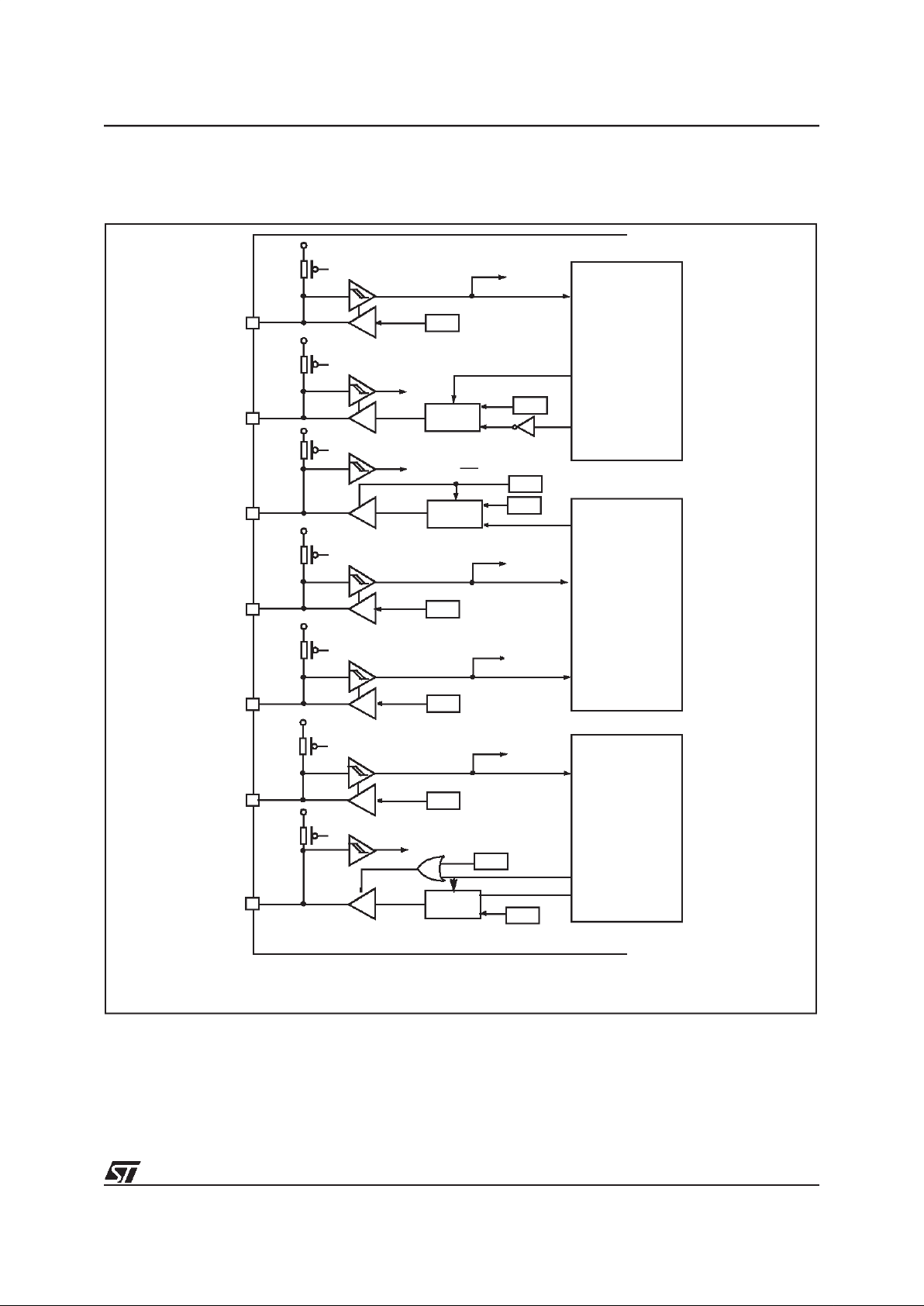
39/84
ST62T28C/E28C
I/O PORTS (Cont’d)
Figure 24. Peripheral Interface Configuration of SPI, UART and AR Timer
PD4/RXD1
PID
0
MUX
1
PD5/TXD1
PD3/Sout
PD2/Sin
PD1/Scl
PA3/ARTIMin
PA2/ARTIMout
V
DD
DR
RXD
UART
IARTOE
TXD
PID
DR
PID
OPR
DR
1
MUX
0
OUT
IN
SYNCHRONOUS
SERIAL I/O
CLOCK
PID
DR
PID
DR
PP/OD
PID
DR
1
MUX
0
ARTIMin
PWMOE
ARTIMER
PID
DR
VR01661D
ARTIMout
OR
39
Page 40

40/84
ST62T28C/E28C
I/O PORTS (Cont’d)
4.1.6 I/O Port Option Registers
ORA/B/C/D (CChPA, CDh PB, CEh PC, CFhPD)
Read/Write
Bit 7-0 = Px7 - Px0:
Port A, B, C, and D Option
Register bits.
4.1.7 I/O Port Data Direction Registers
DDRA/B/C/D(C4h PA,C5h PB, C6h PC, C7hPD)
Read/Write
Bit 7-0 = Px7 - Px0:
Port A, B, C, and D Data Di-
rection Registers bits.
4.1.8 I/O Port Data Registers
DRA/B/C/D (C0h PA, C1hPB, C2h PC, C3h PD)
Read/Write
Bit 7-0 = Px7 - Px0:
Port A, B, C, and D Data Reg-
isters bits.
70
Px7 Px6 Px5 Px4 Px3 Px2 Px1 Px0
70
Px7 Px6 Px5 Px4 Px3 Px2 Px1 Px0
70
Px7 Px6 Px5 Px4 Px3 Px2 Px1 Px0
40
Page 41

41/84
ST62T28C/E28C
4.2 TIMER
The MCU features an on-chip Timer peripheral,
consisting ofan 8-bit counter witha 7-bit programmable prescaler, giving a maximum count of 215.
The peripheral may be configuredin three different
operating modes.
Figure 1 shows the Timer Block Diagram. The external TIMERpin isavailable tothe user. The content of the 8-bit counter can be read/written in the
Timer/Counter register,TCR, whilethe state of the
7-bit prescaler can be read in the PSC register.
The control logic device is managed in the TSCR
register as described in the following paragraphs.
The 8-bit counter is decremented by the output
(rising edge) coming from the 7-bit prescaler and
can be loaded and read under program control.
When it decrements to zero then the TMZ (Timer
Zero) bit in the TSCR is setto “1”. If the ETI (Enable Timer Interrupt) bit in the TSCR is also set to
“1”, aninterrupt request is generated as described
in the Interrupt Chapter. The Timer interrupt can
be used to exit the MCU from WAIT mode.
The prescaler input can be the internal frequency
f
INT
divided by 12 or an external clock applied to
the TIMER pin. The prescaler decrements on the
rising edge. Depending on the division factor programmed by PS2, PS1 and PS0 bits in the TSCR.
The clock input of the timer/counterregister ismultiplexed to different sources. For division factor 1,
the clockinput of the prescaleris alsothat of timer/
counter; for factor 2, bit 0 of the prescaler register
is connected to the clock input of TCR. This bit
changes its stateat halfthe frequency of the prescaler input clock. For factor 4, bit 1 of the PSC is
connected to the clock input of TCR, and so forth.
The prescaler initialize bit, PSI, in the TSCR register must be set to “1” to allow the prescaler (and
hence the counter)to start.If it is cleared to “0”, all
the prescaler bits are set to “1” and the counter is
inhibited from counting. The prescaler can be
loaded with any value between 0 and 7Fh, if bit
PSI is set to “1”. The prescaler tap is selected by
means of the PS2/PS1/PS0 bits in the control register.
Figure 2 illustratesthe Timer’s working principle.
Figure 25. Timer Block Diagram
DATABUS 8
8
8
8
8-BIT
COUNTER
6
5
4
3
2
1
0
PSC
STATUS/CONTROL
REGISTER
b7 b6
b5
b4 b3 b2
b1 b0
TMZ
ETI TOUT
DOUT PSI PS2 PS1 PS0
SELECT
1OF7
3
LATCH
SYNCHRONIZATION
LOGIC
TIMER
INTERRUPT
LINE
VA00009
:12
f
OSC
41
Page 42
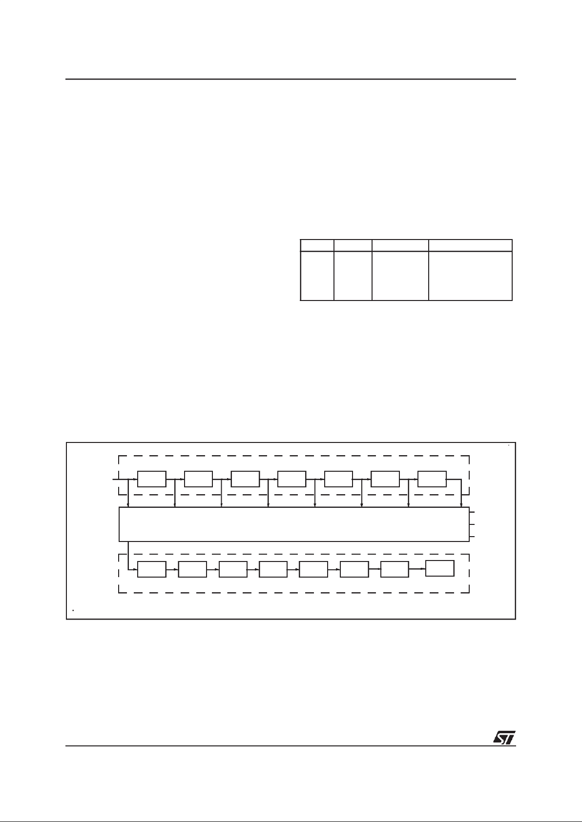
42/84
ST62T28C/E28C
TIMER (Cont’d)
4.2.1 Timer Operating Modes
There are three operating modes, which are selected by the TOUT and DOUT bits (see TSCR
register). These three modes correspond to the
two clocks which can be connected to the 7-bit
prescaler (f
INT
÷ 12 or TIMER pin signal), and to
the output mode.
4.2.1.1 Gated Mode
(TOUT = “0”, DOUT = “1”)
In this mode the prescaler is decremented by the
Timer clock input (f
INT
÷ 12), but ONLY when the
signal on the TIMER pin is held high (allowing
pulse width measurement). This mode is selected
by clearing the TOUT bit in the TSCR register to
“0” (i.e. as input) and setting the DOUTbit to “1”.
4.2.1.2 Event Counter Mode
(TOUT = “0”, DOUT = “0”)
In this mode, the TIMER pin is the input clock of
the prescaler which is decremented on the rising
edge.
4.2.1.3 Output Mode
(TOUT = “1”, DOUT = data out)
The TIMER pin is connected to the DOUT latch,
hence the Timer prescaler is clocked by the prescaler clockinput (f
INT
÷ 12).
The user can select the desiredprescaler division
ratio through the PS2, PS1, PS0 bits. When the
TCR count reaches 0, it sets the TMZ bit in the
TSCR. The TMZ bit can be tested under program
control to perform a timer function whenever it
goes high. The low-to-high TMZ bit transition is
used to latch theDOUT bit of the TSCR and transfer it to the TIMER pin. This operating mode allows
external signal generation on the TIMER pin.
Table 14. Timer Operating Modes
4.2.2 Timer Interrupt
When the counter register decrements to zerowith
the ETI (Enable Timer Interrupt) bit set to one, an
interrupt request is generated as described in the
Interrupt Chapter. When the counter decrements
to zero, the TMZ bit in the TSCR register is set to
one.
Figure 26. Timer Working Principle
TOUT DOUT Timer Pin Timer Function
0 0 Input Event Counter
0 1 Input Gated Input
1 0 Output Output “0”
1 1 Output Output “1”
BIT0 BIT1 BIT2
BIT3
BIT6
BIT5BIT4
CLOCK
7-BIT PRESCALER
8-1 MULTIPLEXER
8-BIT COUNTER
BIT0 BIT1
BIT2
BIT3 BIT4 BIT5
BIT6
BIT7
10234
5
67
PS0
PS1
PS2
VA00186
42
Page 43

43/84
ST62T28C/E28C
TIMER (Cont’d)
4.2.3 Application Notes
TMZ is set when the counter reaches zero; however, it may also be set by writing 00h in the TCR
register or by setting bit 7 of the TSCR register.
The TMZ bit must be cleared by user software
when servicing the timer interrupt to avoid undesired interrupts when leaving the interrupt service
routine. After reset, the 8-bit counter register is
loaded with0FFh, while the7-bit prescaler is loaded with 07Fh, and the TSCR register is cleared.
This means that the Timer is stopped (PSI=“0”)
and the timer interrupt is disabled.
If the Timer is programmed in output mode, the
DOUT bit is transferred to the TIMER pin when
TMZ is set to one (by software or due to counter
decrement). When TMZ is high, the latch is transparent and DOUT is copied to the timer pin. When
TMZ goes low, DOUT is latched.
A write to the TCR register will predominate over
the 8-bit counter decrement to 00h function, i.e.if a
write and a TCR register decrement to 00h occur
simultaneously, the write will take precedence,
and the TMZ bit is not set until the 8-bit counter
reaches 00h again. The values of the TCR and the
PSC registers can be read accurately at any time.
4.2.4 Timer Registers
Timer Status Control Register (TSCR)
Address: 0D4h — Read/Write
Bit 7 = TMZ:
Timer Zero bit
A low-to-high transition indicates that the timer
count register has decrementto zero. This bit must
be cleared by user software before starting a new
count.
Bit 6 = ETI:
Enable Timer Interrupt
When set, enables the timer interrupt request. If
ETI=0 the timer interrupt is disabled. If ETI=1 and
TMZ=1 an interrupt request is generated.
Bit 5 = TOUT:
Timers Output Control
When low, this bit selects the input mode for the
TIMER pin. When high the output mode is selected.
Bit 4 =DOUT:
Data Output
Data sent to the timer outputwhen TMZ isset high
(output mode only). Input mode selection (input
mode only).
Bit 3 =PSI:
Prescaler InitializeBit
Used to initialize the prescalerand inhibit its counting. When PSI=“0” the prescaler is set to 7Fh and
the counter is inhibited. When PSI=“1” the prescaler is enabled to count downwards. As long as
PSI=“0” both counter and prescaler are not running.
Bit 2, 1, 0 = PS2, PS1, PS0:
Prescaler Mux. Se-
lect.
These bits select the division ratio of the pres-
caler register.
Table 15. Prescaler Division Factors
Timer Counter Register TCR
Address: 0D3h — Read/Write
Bit 7-0 = D7-D0:
Counter Bits.
Prescaler Register PSC
Address: 0D2h — Read/Write
Bit 7 =D7: Always read as “0”.
Bit 6-0 = D6-D0: PrescalerBits.
70
TMZ ETI TOUT DOUT PSI PS2 PS1 PS0
PS2 PS1 PS0 Divided by
0001
0012
0104
0118
10016
10132
11064
1 1 1 128
70
D7 D6 D5 D4 D3 D2 D1 D0
70
D7 D6 D5 D4 D3 D2 D1 D0
43
Page 44

44/84
ST62T28C/E28C
4.3 AUTO-RELOAD TIMER
The Auto-Reload Timer (AR Timer) on-chip peripheral consists of an 8-bit timer/counter with
compare and capture/reload capabilities and of a
7-bit prescaler with a clock multiplexer, enabling
the clock input to be selected as f
INT,fINT/3
or an
external clock source. A Mode Control Register,
ARMC, two Status Control Registers, ARSC0 and
ARSC1, an output pin, ARTIMout, and an input
pin, ARTIMin, allow the Auto-Reload Timer to be
used in4 modes:
– Auto-reload (PWMgeneration),
– Output compareand reload on external event
(PLL),
– Inputcapture andoutput compare fortime meas-
urement.
– Input captureand output compare for period
measurement.
The AR Timer can be usedto wakethe MCU from
WAIT mode either with an internal or with an external clock. It also can be used to wake the MCU
from STOP mode, if used with an external clock
signal connected to the ARTIMin pin. A Load register allows the program to read and write the
counter onthe fly.
4.3.1 AR Timer Description
The AR COUNTER is an 8-bit up-counter incremented ontheinput clock’s rising edge. The counter is loaded from the ReLoad/Capture Register,
ARRC, for auto-reload or capture operations, as
well as for initialization. Direct access to the AR
counter is not possible; however, by reading or
writing the ARLR load register, it is possible to
read or write the counter’s contents on thefly.
The AR Timer’s input clock can beeither the internal clock (from the Oscillator Divider), the internal
clock divided by 3, or theclock signal connected to
the ARTIMin pin. Selection between these clock
sources is effected by suitably programming bits
CC0-CC1 of the ARSC1 register. The output of the
AR Multiplexer feeds the 7-bit programmable AR
Prescaler, ARPSC, which selects one of the 8
available taps of the prescaler, as defined by
PSC0-PSC2 in the AR Mode Control Register.
Thus the division factor of the prescalercan be set
to 2n (where n = 0, 1,..7).
The clock input tothe ARcounter isenabled bythe
TEN (Timer Enable) bit in the ARMC register.
When TEN isreset, the AR counter is stopped and
the prescaler and counter contents are frozen.
When TEN is set, the AR counter runs at the rate
of the selected clock source. The counter is
cleared on system reset.
The AR counter may also be initialized by writing
to the ARLR load register, which also causes an
immediate copy of the value tobe placed in the AR
counter, regardless of whether the counter is running or not. Initialization of the counter, by either
method, will also clearthe ARPSC register, whereupon counting will start from a known value.
4.3.2 Timer Operating Modes
Four different operating modes are available for
the AR Timer:
Auto-reload Mode with PWM Generation. This
mode allows a Pulse Width Modulated signal to be
generated on the ARTIMout pin with minimum
Core processing overhead.
The free running 8-bit counter is fed by the prescaler’s output, and is incremented on every rising
edge of the clock signal.
When a counter overflow occurs, the counter is
automatically reloadedwith thecontents ofthe Reload/Capture Register, ARCC, and ARTIMout is
set. When the counter reaches the value contained in the compare register (ARCP), ARTIMout
is reset.
On overflow, the OVF flag of the ARSC0 registeris
set and an overflow interrupt request is generated
if the overflow interrupt enable bit, OVIE, in the
Mode Control Register (ARMC), is set. The OVF
flag must be reset by the user software.
When the counterreaches thecompare value, the
CPF flag of the ARSC0 register is set and a compare interrupt request isgenerated, if the Compare
Interrupt enable bit, CPIE, in the Mode Control
Register (ARMC), is set. Theinterrupt service routine may then adjust thePWM period by loading a
new value intoARCP. TheCPF flag must be reset
by user software.
The PWM signal is generated on the ARTIMout
pin (refer to the Block Diagram). The frequency of
this signal is controlled by the prescaler setting
and by the auto-reload value present in the Reload/Capture register, ARRC. The duty cycle of
the PWM signal is controlledby theCompare Register, ARCP.
44
Page 45

45/84
ST62T28C/E28C
AUTO-RELOAD TIMER (Cont’d)
Figure 27. AR Timer Block Diagram
DATA BUS
8
8
8
COMPARE
8
RELOAD/CAPTURE
DATA BUS
AR TIMER
VR01660B
88
R
S
TCLD
OVIE
PWMOE
OVF
LOAD
ARTIMout
M
SYNCHRO
ARTIMin
SL0-SL1
INT
f
PA3/
AR
REGISTER
EF
REGISTER
LOAD
AR
U
X
f
INT
/3
AR PRESCALER
7-Bit
CC0-CC1
AR COUNTER
8-Bit
AR COMPARE
REGISTER
OVF
EIE
EF
INTERRUPT
CPF
CPIE
CPF
DRA2
DDRA2
PA2/
PS0-PS2
88
45
Page 46

46/84
ST62T28C/E28C
AUTO-RELOAD TIMER (Cont’d)
It should be noted that the reload values will also
affect the value and the resolution of the duty cycle
of PWM output signal. To obtain a signal on ARTIMout, the contents of the ARCP register must be
greater thanthe contents of the ARRC register.
The maximum available resolution for the ARTIMout duty cycle is:
Resolution = 1/[255-(ARRC)]
Where ARRC is the content of the Reload/Capture
register. The compare value loaded in the Compare Register, ARCP, must be in the range from
(ARRC) to 255.
The ARTC counter is initialized by writing to the
ARRC register and by thensetting theTCLD (Timer Load) andthe TEN (Timer Clock Enable) bits in
the Mode Control register, ARMC.
Enabling and selection of the clock source is controlled by the CC0, CC1, SL0 and SL1 bits in the
Status Control Register, ARSC1. Theprescaler division ratio is selected by the PS0, PS1 and PS2
bits in the ARSC1 register.
In Auto-reload Mode, any of the three available
clock sources can be selected: Internal Clock, Internal Clock divided by 3 or the clock signal
present on the ARTIMin pin.
Figure 28. Auto-reload Timer PWM Function
COUNTER
COMPARE
VALUE
RELOAD
REGISTER
PWM OUTPUT
t
t
255
000
VR001852
46
Page 47

47/84
ST62T28C/E28C
AUTO-RELOAD TIMER (Cont’d)
Capture Mode with PWM Generation.Inthis
mode, the AR counter operates as a free running
8-bit counter fed by the prescaler output. The
counter isincremented onevery clock risingedge.
An 8-bit capture operation from the counter to the
ARRC register is performed on every active edge
on the ARTIMin pin, when enabled by Edge Control bits SL0, SL1 in the ARSC1 register. At the
same time, the External Flag, EF, in the ARSC0
register is set and an external interrupt request is
generated if the External Interrupt Enable bit, EIE,
in the ARMC register, is set. The EF flag must be
reset by user software.
Each ARTC overflow sets ARTIMout, while a
match between the counter and ARCP (Compare
Register) resets ARTIMout and sets the compare
flag, CPF.A compareinterrupt request isgenerated if the related compare interrupt enable bit,
CPIE, isset. A PWM signalis generated on ARTIMout. The CPF flag must be reset by user software.
The frequency of the generated signal is determined by the prescaler setting. The duty cycle is
determined by the ARCP register.
Initialization and reading of thecounter are identical tothe auto-reload mode (see previousdescription).
Enabling andselection of clock sources is controlled by the CC0 and CC1 bits in the ARStatus Control Register, ARSC1.
The prescaler division ratio is selected by programming the PS0, PS1 and PS2 bits in the
ARSC1 Register.
In Capture mode, the allowed clock sources are
the internalclock and the internal clock divided by
3; the external ARTIMin input pin should not be
used asa clock source.
Capture Mode with Reset of counter and prescaler, and PWM Generation. This mode is identi-
cal to the previous one, with the difference that a
capture condition also resets the counter and the
prescaler, thus allowing easy measurement of the
time between two captures (for input period measurement on the ARTIMin pin).
Load on External Input. Thecounter operates as
a free running 8-bit counter fed by the prescaler.
the count is incremented on every clock rising
edge.
Each counter overflow sets the ARTIMout pin. A
match between the counter and ARCP (Compare
Register) resets the ARTIMout pin and sets the
compare flag, CPF. A compareinterrupt request is
generated if the related compare interrupt enable
bit, CPIE, is set. A PWM signal is generated on
ARTIMout. The CPF flag must be reset by user
software.
Initialization of the counter is as described in the
previous paragraph. In addition, ifthe externalARTIMin input is enabled,an active edge onthe input
pin will copy the contents ofthe ARRC register into
the counter, whether the counter is runningor not.
Notes:
The allowed AR Timer clock sources are the fol-
lowing:
The clock frequency should not be modified while
the counter is counting, since the counter may be
set to an unpredictable value. For instance, the
multiplexer setting should not be modified while
the counter is counting.
Loading of the counter by any means (by auto-reload, through ARLR, ARRC or by the Core) resets
the prescaler at the same time.
Care should be taken when boththe Capture interrupt and the Overflow interrupt are used. Capture
and overflow are asynchronous. If the capture occurs when the Overflow Interrupt Flag, OVF, is
high (between counteroverflow and the flagbeing
reset by software, in the interruptroutine), the External Interrupt Flag, EF, may be cleared simultaneusly without the interrupt being taken into account.
The solution consists in resetting the OVF flag by
writing 06h in the ARSC0 register. Thevalue of EF
is not affectedby this operation. If aninterrupt has
occured, it will be processed when the MCU exits
from the interrupt routine (the second interrupt is
latched).
AR Timer Mode Clock Sources
Auto-reload mode f
INT,fINT/3
, ARTIMin
Capture mode f
INT,fINT/3
Capture/Reset mode f
INT,fINT/3
External Load mode f
INT,fINT/3
47
Page 48

48/84
ST62T28C/E28C
AUTO-RELOAD TIMER (Cont’d)
4.3.3 AR Timer Registers
AR Mode Control Register (ARMC)
Address: E5h — Read/Write
Reset status:00h
The AR Mode Control Register ARMC is used to
program the different operating modes of the AR
Timer, to enable the clock and to initialize the
counter. It can be read and written to by the Core
and it is cleared on system reset (the AR Timer is
disabled).
Bit 7 = TLCD:
Timer Load Bit.
This bit, when set,
will cause the contents of ARRC register to be
loaded into the counter and the contents of the
prescaler register,ARPSC, are cleared in order to
initialize the timer before starting to count. This bit
is write-only and any attempt to read it will yield a
logical zero.
Bit 6 = TEN
: Timer Clock Enable.
This bit, when
set, allows the timer to count. When cleared, it will
stop the timer and freeze ARPSC and ARTSC.
Bit 5 = PWMOE:
PWM Output Enable.
This bit,
when set, enables the PWM output on the ARTIMout pin. When reset, thePWM output is disabled.
Bit 4 = EIE:
External Interrupt Enable.
This bit,
when set, enables the external interrupt request.
When reset, the external interrupt request is
masked. If EIE is set and the related flag, EF, in
the ARSC0 register is also set, an interrupt request is generated.
Bit 3 = CPIE:
Compare Interrupt Enable.
This bit,
when set, enables the compare interrupt request.
If CPIE is reset, the compare interrupt request is
masked. If CPIE is set and the related flag, CPF, in
the ARSC0 register is also set, an interrupt request is generated.
Bit 2 = OVIE:
Overflow Interrupt
. This bit, when
set, enables the overflow interrupt request. If OVIE
is reset, the compare interrupt request is masked.
If OVIE is set and the related flag, OVF in the
ARSC0 register is also set, an interrupt request is
generated.
Bit 1-0= ARMC1-ARMC0:
Mode Control Bits 1-0
.
These are the operating mode control bits. The following bit combinations will select the various operating modes:
AR Timer Status/Control Registers ARSC0 &
ARSC1. Theseregisters contain the AR Timer sta-
tus information bits and also allow the programming of clock sources, active edge and prescaler
multiplexer setting.
ARSC0 register bits 0,1 and 2 containthe interrupt
flags of theAR Timer. Thesebits are read normally. Each one may be reset by software. Writing a
one does not affect thebit value.
AR Status Control Register 0 (ARSC0)
Address: E6h — Read/Clear
Bits 7-3 = D7-D3:
Unused
Bit 2= EF:
External Interrupt Flag.
This bit isset by
any active edge on the external ARTIMin input pin.
The flag is cleared bywriting a zero to the EF bit.
Bit 1 = CPF:
Compare Interrupt Flag.
This bit is set
if the contents of the counter and the ARCP register areequal. The flag is cleared by writing a zero
to the CPF bit.
Bit 0 = OVF:
Overflow InterruptFlag.
This bitis set
by a transition of the counter from FFh to 00h
(overflow). The flag is cleared by writing a zero to
the OVF bit.
70
TCLD TEN PWMOE EIE CPI E OV IE AR MC1 ARMC0
ARMC1 ARMC0 Operating Mode
0 0 Auto-reload Mode
0 1 Capture Mode
10
Capture Mode with Reset
of ARTC and ARPSC
11
Load on External Edge
Mode
70
D7 D6 D5 D4 D3 EF CPF OVF
48
Page 49

49/84
ST62T28C/E28C
AUTO-RELOAD TIMER (Cont’d)
AR Status Control Register 1(ARSC1)
Address: E7h — Read/Write
Bist 7-5 = PS2-PS0:
Prescaler Division Selection
Bits 2-0.
These bits determine the Prescaler division ratio. The prescaler itself is not affected by
these bits.Theprescaler division ratioislistedinthe
following table:
Table 16. Prescaler Division Ratio Selection
Bit 4 = D4:
Reserved
. Mustbe kept reset.
Bit 3-2= SL1-SL0:
Timer InputEdgeControl Bits 1-
0.
These bits control theedge function of the Timer
inputpinfor externalsynchronization. IfbitSL0isreset, edgedetectionis disabled;ifset edgedetection
is enabled.Ifbit SL1 isreset, the ARTimer inputpin
is rising edgesensitive; if set, it is fallingedge sensitive.
Bit 1-0 = CC1-CC0:
Clock Source Select Bit 1-0.
These bits select theclock source for theAR Timer
through the AR Multiplexer. The programming of
the clocksources isexplainedin thefollowingTable
17:
Table 17. Clock Source Selection.
AR Load Register ARLR. The ARLRload register
is used to read or write the ARTC counter register
“on the fly” (while it is counting). The ARLR register is not affected by system reset.
AR Load Register (ARLR)
Address: EBh — Read/Write
Bit 7-0 = D7-D0:
Load Register Data Bits.
These
are the load register data bits.
AR Reload/Capture Register. The ARRC reload/
capture register is used to hold the auto-reload
value whichis automatically loaded into the counter when overflow occurs.
AR Reload/Capture (ARRC)
Address: E9h — Read/Write
Bit 7-0 = D7-D0:
Reload/Capture Data Bits
. These
are the Reload/Capture register data bits.
AR Compare Register. The CP compare register
is used to holdthe compare value for the compare
function.
AR Compare Register (ARCP)
Address: EAh — Read/Write
Bit 7-0 = D7-D0:
Compare Data Bits
. These are
the Compare register data bits.
70
PS2 PS1 PS0 D4 SL1 SL0 CC1 CC0
PS2 PS1 PS0 ARPSC Division Ratio
0
0
0
0
1
1
1
1
0
0
1
1
0
0
1
1
0
1
0
1
0
1
0
1
1
2
4
8
16
32
64
128
SL1 SL0 Edge Detection
X 0 Disabled
0 1 Rising Edge
1 1 Falling Edge
CC1 CC0 Clock Source
00F
int
01F
int
Divided by 3
1 0 ARTIMin Input Clock
1 1 Reserved
70
D7 D6 D5 D4 D3 D2 D1 D0
70
D7 D6 D5 D4 D3 D2 D1 D0
70
D7 D6 D5 D4 D3 D2 D1 D0
49
Page 50

50/84
ST62T28C/E28C
4.4 A/D CONVERTER (ADC)
The A/D converter peripheral is an 8-bit analog to
digital converter with analoginputs asalternate I/O
functions (the number of which is device dependent), offering 8-bit resolution with a typical conversion time of 70us (at an oscillator clock frequency
of 8MHz).
The ADC converts the input voltage by a process
of successive approximations, using a clock frequency derived from the oscillator with a division
factor of 12 or 6. After Reset, divisionby 12 is used
by default to insure compatibility with other members of the ST62 MCU family. With an oscillator
clock frequency less than 1.2MHz, conversion accuracy is decreased.
Selection of the input pin is done by configuring
the related I/O line as an analog input via the Option and Data registers (refer to I/O ports description for additional information). Only one I/O line
must be configured as an analog input at any time.
The user must avoid any situation in which more
than one I/O pin is selected as an analog input simultaneously, toavoid device malfunction.
The ADC uses two registers in the data space:the
ADC data conversion register, ADR, which stores
the conversion result, and the ADC control register, ADCR,used to program the ADC functions.
A conversionis started by writinga “1” to theStart
bit (STA) in the ADC control register. This automatically clears (resets to “0”) the End Of Conversion Bit (EOC). When a conversion is complete,
the EOC bit is automatically set to “1”, in order to
flag that conversion is complete and that the data
in the ADC data conversion registeris valid. Each
conversion has to be separately initiated bywriting
to the STA bit.
The STA bit is continuously scanned so that, ifthe
user sets it to “1” while a previous conversion is in
progress, a new conversion is started before completing the previous one. The start bit (STA) is a
write onlybit, anyattempt to read it will show a logical “0”.
The A/D converter features a maskable interrupt
associated with the end of conversion. This interrupt is associated with interrupt vector #4 and occurs when the EOC bit is set (i.e. when a conversion is completed). The interrupt is masked using
the EAI(interrupt mask) bit in the control register.
The power consumption of the device can be reduced by turning off the ADC peripheral. This is
done by setting the PDS bit in theADC control register to “0”. If PDS=“1”, the A/D is powered andenabled for conversion. This bit must be set at least
one instruction before thebeginning ofthe conversion to allow stabilisation of the A/D converter.
This action is also needed before entering WAIT
mode, since the A/D comparator is not automatically disabled in WAIT mode.
During Reset, any conversion in progress is
stopped, thecontrol register is reset to 40h and the
ADC interrupt is masked (EAI=0).
Figure 29. ADC Block Diagram
4.4.1 Application Notes
The A/D converter does not feature a sample and
hold circuit. The analog voltage to be measured
should therefore be stable during the entire conversion cycle. Voltage variation should not exceed
±1/2 LSB for the optimum conversion accuracy. A
low pass filter may be used at the analog input
pins to reduce input voltage variation during conversion.
When selected asan analog channel, the input pin
is internally connected to a capacitor Cadof typically 12pF. For maximum accuracy, this capacitor
must be fully charged at the beginning of conversion. In the worst case, conversion starts one instruction (6.5 µs) after the channel has been selected. In worst case conditions, the impedance,
ASI, of the analog voltage sourceis calculatedusing the following formula:
6.5µs=9xCadx ASI
(capacitor charged to over 99.9%), i.e. 30 kΩ including a 50% guardband. ASI can behigher if C
ad
has been charged for a longer period by adding instructions before the start of conversion (adding
more than 26 CPU cycles is pointless).
CONTROL REGISTER
CONVERTER
VA00418
RESULT REGISTER
RESET
INTERRUPT
CLOCK
AV
AV
DD
Ain
8
CORE
CONTROL SIGNALS
SS
8
CORE
50
Page 51

51/84
ST62T28C/E28C
A/D CONVERTER (Cont’d)
Since the ADC is on the same chip as the microprocessor, the usershould not switch heavilyloaded output signals during conversion, if high precision is required.Such switchingwill affectthe supply voltages used as analog references.
The accuracy of the conversion depends on the
quality of the power supplies (VDDand VSS). The
user musttake special care to ensure a well regulated reference voltage is present on the VDDand
VSSpins (power supply voltage variations mustbe
less than5V/ms). This implies, in particular, that a
suitable decoupling capacitor is used at the V
DD
pin.
The converter resolution is given by:
The Input voltage (Ain) which is to be converted
must be constant for 1µs before conversion and
remain constant during conversion.
Conversion resolution canbe improved ifthe power supply voltage (VDD) to the microcontroller is
lowered.
In orderto optimise conversion resolution, the user
can configure the microcontroller in WAIT mode,
because this mode minimises noise disturbances
and power supply variations due to output switching. Nevertheless, the WAIT instruction should be
executed as soon as possible after the beginning
of the conversion, because execution of theWAIT
instruction may cause a small variation of the V
DD
voltage. The negative effectof this variation is minimized at the beginning ofthe conversion when the
converter is less sensitive, rather than at the end
of conversion, when the less significant bits are
determined.
The best configuration, from an accuracy standpoint, is WAIT mode with the Timer stopped. Indeed, only the ADC peripheral and the oscillator
are thenstill working. The MCU must be woken up
from WAIT mode by the ADC interrupt at the end
of the conversion. It should be noted that waking
up the microcontroller could also be done using
the Timer interrupt, but in this case the Timer will
be working and the resulting noise could affect
conversion accuracy.
One extra feature is available in the ADC to get a
better accuracy. Infact, eachADC conversion has
to be followed by a WAIT instruction to minimize
the noise during the conversion. But the first conversion step is performed before the execution of
the WAITwhen most of clocks signals are still enabled . The key is to synchronize the ADC start
with the effective execution of the WAIT. This is
achieved by setting ADC SYNC option. This way,
ADC conversion starts in effective WAIT for maximum accuracy.
Note: With this extra option, it ismandatory to execute WAIT instruction just after ADCstart instruction. Insertion of any extra instruction may cause
spurious interrupt request at ADC interrupt vector.
A/D Converter Control Register (ADCR)
Address: 0D1h — Read/Write
Bit 7 = EAI:
Enable A/D Interrupt.
If this bit is setto
“1” the A/D interrupt is enabled, when EAI=0 the
interrupt is disabled.
Bit 6 = EOC:
End of conversion. Read Only
. This
read only bit indicates when a conversion has
been completed. This bit is automatically reset to
“0” when the STA bit is written. If the user is using
the interrupt optionthen this bit can beused as an
interrupt pending bit. Data in the data conversion
register are valid only whenthis bit is set to “1”.
Bit 5 =STA
: Startof Conversion. Write Only
. Writing a “1” to this bitwill start a conversion onthe selected channel and automatically reset to “0” the
EOC bit. If the bit is set again when a conversion is
in progress, the present conversion is stopped and
a new one will take place. This bit is write only, any
attempt to read it will show a logical zero.
Bit 4 = PDS
: Power Down Selection.
This bit activates the A/D converter if setto “1”.Writing a “0” to
this bit will put the ADC in power down mode (idle
mode).
Bit 3= CLSEL:
Clock Selection
. When set, the
ADC is drivenby theMCU internal clockdivided by
6, and typical conversion time at 8MHz is 35µs.
When cleared (Reset state), MCU clock divided by
12 is used with a typical 70µs conversion time at
8MHz.
Bit 2 = OSCOFF. When low, this bit enables main
oscillator to run. Themain oscillatoris switched off
when OSCOFF is high.
Bit 1-0: Reserved. Must bekept cleared.
A/D Converter Data Register (ADR)
Address: 0D0h — Read only
Bit 7-0 = D7-D0
: 8Bit A/D Conversion Result.
V
DDVSS
–
256
----------------------------
70
EAI EOC STA PDS CLSEL
OSC
OFF
D1 D0
70
D7 D6 D5 D4 D3 D2 D1 D0
51
Page 52

52/84
ST62T28C/E28C
4.5 U. A. R. T. (Universal Asynchronous Receiver/Transmitter)
The UART provides the basic hardware for asynchronous serial communication which, combined
with anappropriate software routine, gives a serial
interface providing communication with common
baud rates (up to 76,800 Baud with an 8MHz external oscillator) and flexible characterformats.
Operating in Half-Duplex mode only, the UART
uses a 10-bit frame or a 11-bit frame according to
the choosenMCU option. Automatic parity bit generation is software selectable in the 10-bit character format allowing either 7 data bit + 1 paritybit, or
8 data bittransmission. Transmitted datais sent directly, whilereceived datais buffered allowing further data characters to be received while the data
is beingreadout of the receive buffer register. Data
transmit has priority over databeing received.
The UART is supplied with an MCU internal clock
thatisalso availableinWAITmodeoftheprocessor.
4.5.1 Ports Interfacing
RXD reception line and TXD emission line are
sharing the same external pins as two I/O lines.
Therefore, UART configuration requires to set
these two I/O lines through the relevant ports registers. The I/O line common with RXD line must be
defined as input mode (with or without pull-up)
while the I/O line common with TXD line must be
defined as output mode (Push-pull oropen drain).
In the 11-bit character format option, the transmitted data isinverted and can therefore use a single
transistor buffering stage. Defined as input, the
RXD line can be read at any time as an I/O line
during the UART operation.The TXD pin follows I/
O port registers value when UARTOE bit is
cleared, which means when no serial transmission
is in progress. As a consequence, a permanent
high level has to be written onto the I/O port in order to achieve a proper stop condition on the TXD
line when no transmission is active.
Figure 30. UART Block Diagram
CONTROL LOGIC
TO CORE
START
DETECTOR
DATA SHIFT
REGISTER
D8 D7 D6 D5 D4 D3D2 D1 D0
CONTROL REGISTER
BAUD RATE
RECEIVE BUFFER
REGISTER
PROGRAMMABLE
DIVIDER
DIN DOUT
D8
BAUD RATE x 8
WRITE
READ
RXD1
TXD1
UARTOE
RX and TX
INTERRUPTS
TXD
DR
0
MUX
1
f
OSC
VR02009
52
Page 53

53/84
ST62T28C/E28C
U. A. R. T (Cont’d)
4.5.2 Clock Generation
The UART contains a built-in divider of the MCU
internal clock for most common Baud Rates as
shown in Table 19. Other baud rate values can be
calculated from the chosen oscillator frequency divided by the Divisor value shown.
The divided clock provides a frequency that is 8
times the desired baud rate. This allows the Data
reception mechanism to provide a 2 to 1 majority
voting system to determine the logic state of the
asynchronous incoming serial logic bit by taking 3
timed samples within the 8 time states.
The bits not sampled provide a buffer to compensate for frequency offsets between sender and receiver.
4.5.3 Data Transmission
Whatever the format selected as MCU option, 10bit or 11-bit frame, the start and stop bit are automatically generated by the UART. Only the remaining 8 (Resp. 9) bit in the 10-bit (Resp. 11-bit)
frame are under control of the user.
Transmission is started bywriting the DataRegister, after having previously set the transmission
software options, the baudrate and the parity enable. In case of 11-bit frame, the 9th bit must then
be set before into the LSB of the UART Control
Register. Bit 9 remains in the state programmed
for consecutive transmissions until changed by the
user oruntil a character is received when thestate
of this bit is changed to thatof theincoming bit 9.
The UARTOE signal switches the output multiplexer tothe UART output and a start bit is sent (a
0 for one bit time) followedby the data bit with the
LSB D0 at first.. The output is then set to 1 for a
period of one bit time to generate a Stop bit, and
then the UARTOE signal returns the TXD1 line to
its alternate I/O function. The end of transmission
is flagged by setting TXMT to 1 and an interrupt is
generated if enabled. The TXMT flag is reset by
writing a 0 to the bit position, it is also cleared automatically when a new character is written to the
Data Register. TXMT can be set to 1 by software
to generate a software interrupt so care must be
taken in manipulating the Control Register.
4.5.3.1 Character Format
Once the MCU option is set as 10-bit or 11-bit
frame, the framelength is fixed. Within these8 or9
remaining bit, anyformat can beused asshown in
the Table 18. Only the evenparity automatic computation in the 10-bit frame is available. Any other
parity bit can however be software computed and
processed as adata bit
Table 18. Character Options
Figure 31. 11-bit Character Format Example
Figure 32. UART Data Output
10 bit frame
Start Bit 8 Data No Parity 1 Stop
Start Bit 7 Data 1 Even Parity (Auto) 1 Stop
Start Bit 7 Data 1 Software Parity 1 Stop
11 bit frame
Start Bit 8 Data 1 Software Parity 1 Stop
Start Bit 9 Data No Parity 1 Stop
Start Bit 8 Data No Parity 2 Stop
Start Bit 7 Data 1 Software Parity 2 Stop
VR02012
POSITION
1
28
10
BIT
BIT
START STOP
BIT
POSSIBLE
NEXT
CHARACTER
START
D0 D1 D7 D8
START OF DATA
9
TXD1
TXD
PORT DATA
0
MUX
1
OUTPUT
UARTOE
VR02011
53
Page 54
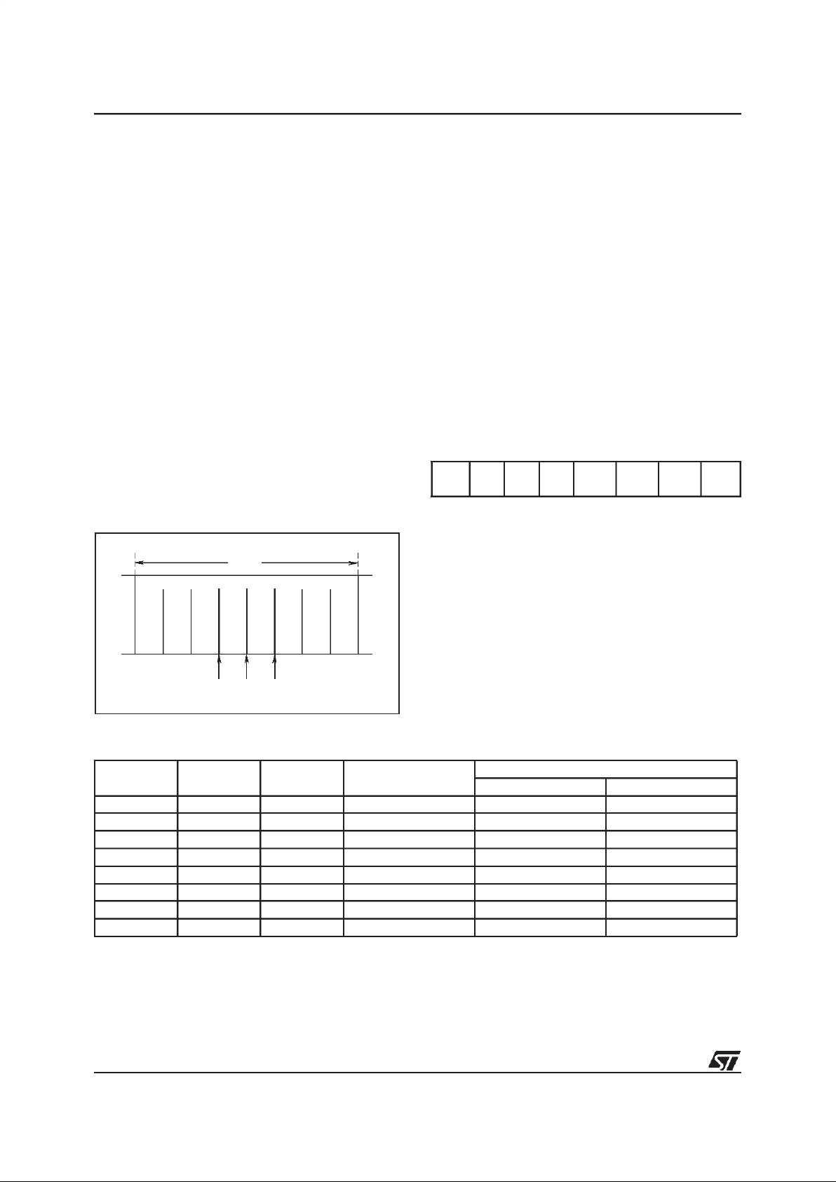
54/84
ST62T28C/E28C
U. A. R. T (Cont’d)
4.5.4 Data Reception
The UART continuously looks for a falling edge on
the input pin whenever a transmission is not active. Once anedge is detectedit waits 1bit time (8
states) toaccommodate theStart bit,and then assembles the following serial data stream into the
data register. First 8 bit are stored into the UART
Data Register, while the additionnal 9th bit is
stored into theLSB of the UART Control Register
in case of the 11-bit frame MCU option has been
selected. Whenthe 10-bit frame optionis selected,
the parityof the 8 received bitis automatically written into the LSB of the UART Control Register
(PTYEN bit).
After allbit havebeen received, the Receiver waits
for the duration of one bit (for the Stop bit) and
then transfers thereceived datainto the buffer register, allowing a following character to be received.
The interrupt flag RXRDY isset to 1 as the data is
transferred to the buffer register and, if enabled,
will generatean interrupt.
Figure 33. Data Sampling Points
If a transmission is started during the course of a
reception, the transmission takes priority and the
reception is stopped to free the resources for the
transmission. This implies that a handshaking system must be implemented, as polling of the UART
to detect reception is not available.
4.5.5 Interrupt Capabilities
Both reception andtransmission processes can induce interrupt to the core as defined in the interrupt section. These interrupts are enabled by setting TXIEN and RXIENbit in the UARTCR register,
and TXMT and RXRDY flags are set accordingly
to the interrupt source.
4.5.6 Registers
UART Data Register (UARTDR)
Address: D6h, Read/Write
Bit7-Bit0.
UART data bits
. A write to this register
loads the data into the transmit shift register and
triggers the start of transmission. In addition this
resets the transmit interrupt flag TXMT. A read of
this register returns the data from the Receive
buffer. If the automatic even parity computation is
set (Bit PTYEN set), D7 must be cleared to 0 before transmission. Only the 7 LSB D0..D6 contain
the data to be sent.
Warning
. No Read/Write Instructions may be
used with this registeras both transmit and receive
share the same address
Table 19. Baudrate Selection
VR02010
1 BIT
012 345678
SAMPLES
70
D7 D 6 D5 D4 D3 D2 D1 D0
BR2 BR1 BR0 f
INT
Division
Baud Rate
f
INT
= 8MHz f
INT
= 4MHz
0 0 0 6.656 1200 600
0 0 1 3.328 2400 1200
0 1 0 1.664 4800 2400
0 1 1 832 9600 4800
1 0 0 416 19200 9600
1 0 1 256 31200 15600
1 1 0 208 38400 19200
1 1 1 104 76800 38400
54
Page 55

55/84
ST62T28C/E28C
U. A. R. T (Cont’d)
UART Control Register (UARTCR)
Address: D7h, Read/Write
Bit 7 = RXRDY.
Receiver Ready
. This flag becomes active as soon as a complete byte has
been received and copiedinto thereceive buffer. It
may be cleared by writing a zero to it. Writing a
one is possible.If the interruptenable bitRXIEN is
set to one, a software interrupt will be generated.
Bit 6 = TXMT.
Transmitter Empty
. This flag becomes active as soon as a complete byte has
been sent. It maybe cleared bywriting a zero to it.
It isautomatically cleared by the action ofwriting a
data valueinto the UART data register.
Bit 5 = RXIEN.
Receive Interrupt Enable
. When
this bit is set to 1, the receive interrupt is enabled.
Writing to RXIEN does not affect the status of the
interrupt flag RXRDY.
Bit 4 = TXIEN.
Transmit Interrupt Enable
. When
this bit is setto 1,the transmitinterrupt is enabled.
Writing to TXIEN does not affect the status of the
interrupt flag TXRDY.
Bit 3-1= BR2..BR0.
Baudrate select
. These bits
select the operating baud rate of the UART, depending onthe frequency offOSC. Care should be
taken not to change these bitsduring communication as writing to these bits has an immediate effect.
Bit 0 = PTYEN.
Parity/Data Bit 8
. The function of
this bit depens on the MCU option set. In 11-bit
frame mode, it is the 9th bit of the trasmitted/received character. In 10-bit frame mode,writing a 1
enables the automatic even parity computation,
while a read instruction after reception gives the
parity of the whole 8 bit word received. For the
even parity, a 0 value means no parity error.
Note: As the PTYEN bit ismodified in reception, it
must be to set to 1 before transmission if a reception occured in between.
70
RXRDY TXMT RXIEN TXIEN BR2 BR1 BR0 PTYEN
55
Page 56

56/84
ST62T28C/E28C
4.6 SERIAL PERIPHERAL INTERFACE(SPI)
The on-chip SPI is an optimized serial synchronous interface that supports a widerange ofindustry standard SPI specifications. The on-chip SPI is
controlled by small and simple user software to
perform serial data exchange. The serial shift
clock can be implemented either by software (using the bit-set and bit-reset instructions), with the
on-chip Timer 1 by externally connecting the SPI
clock pinto the timer pin or by directly applying an
external clock to theScl line.
The peripheral is composed by an 8-bit Data/shift
Register and a 4-bit binary counter while the Sin
pin is the serial shift input and Sout is the serial
shift output. These two lines can be tied together
to implement two wires protocols (I C-bus, etc).
When data is serialized, the MSBis the first bit. Sin
has to be programmed a s input. For serial output
operation Sout has to be programmed as opendrain output.
The SCL, Sin andSout SPI clock anddata signals
are connected to 3 I/O lines on the sam e external
pins. With these 3lines, the SPI canoperate in the
following operating modes: Software SPI, S-BUS,
I C-bus and as a standard serial I/O (clock, data,
enable). An interruptrequest can be generated after eight clock pulses. Figure 34 shows the SPI
block diagram.
The S CL line clocks, on the falling edge, the shift
register and the counter.To allow SPI operation in
slave mode, the SCL pin must be programmed as
input and an external clock must be supplied to
this pin to drive the SPI peripheral.
WARNING: In all cases, in both slave and master
mode, the SCL pin must always be configured as
input (Reset state).
In mast er mode, the SCL signal must be generated by software andoutput on another free I/O port
pin which must beconnected externallyto the SCL
input pin.
Figure 34. SPI Block Diagram
Set Res
CLK
RESET
4-Bit Counter
(Q4=High after Clock8)
Data Reg
Direction
I/O Port
8-Bit Data
Shift Register
Reset
Load
DOUT
Output
Enable
8-Bit Tristate Data I/O
RESET
I/O Port
I/O Port
CP
CP
DIN
D0..... ......... ..............D7
to Processor Data Bus
Q4
Q4
OPR Reg.
DIN
SCL
Sin
Sout
SPI Inter rupt Disable Regist er
SPI Data Register
Data Reg
Direction
Data Reg
Direction
DOUT
Write
Read
MUX
0
1
Interrupt
VR01504
56
Page 57

57/84
ST62T28C/E28C
SERIAL PERIPHERAL INTERFACE (Cont’d)
After 8 clock pulses (D7..D0) the output Q4 of the
4-bit binary counter becomes low, disabling the
clock from the counter and the data/shift register.
Q4 enables the clock to generate an interrupt on
the 8thclock falling edge as long as no reset of the
counter (processor write into the 8-bit data/shift
register) takes place. After a processor reset the
interrupt is disabled. The interrupt is active when
writing data in the shift register and desactivated
when writing any data in the SPI Interrupt Disable
register.
The generation of an interrupt to the Core provides
information that newdata is available (inputmode)
or that transmission is completed (output mode),
allowing the Core to generate an acknowledge on
the 9th clock pulse (I C-bus).
The interrupt is initiated by a highto lowtransition,
and therefore interruptoptions mustbe set accordingly as defined in theinterrupt section.
After power on reset, or after writing the data/shift
register, the counter is reset t o zero and the clock
is enabled. In t his condition the data shift register
is readyfor reception. No start condition has to be
detected. Through the user software the Core may
pull down the Sin line ( Acknowledge) and slow
down the SCL, as long as it is needed to carry out
data from the shift register.
I C-bus Master-Slave, Receiver-Transmitter
When pins Sin and Sout are externally connected
together it is possible to use the SPI as a receiver
as well as a transmitter. Through software routine
(by using bit-set and bit-reset on I/O line) a clock
can be generated allowing I C-bus to workin master mode.
When implementing an I C-bus protocol, the start
condition can bedetected by settingthe processor
into a wait for start condition by enabling the interrupt of the I/O port used for the Sin line. This frees
the processor from polling the Sin and S CL lines.
After thetransmission/reception theprocessor has
to poll for the STOP condition.
In slave mode the user software can slow down
the SCLclock frequency bysimply putting the SCL
I/O line in output open-drain mode and wri ting a
zero intothe corresponding data register bit.
As it is possible to directlyread the Sin pin directly
through the port register, the software can detect a
difference between internal dataand external data
(master mode). Similar conditioncan be applied to
the clock.
Three (Four) Wire Serial Bus
It is possible to use a single general purpose I/O
pin (with the corresponding interruptenabled) as a
chip enable pin. SCL acts as active or passive
clock pin, Sinas data in and Sout as data out (four
wire bus). Sin andSout canbe connected together
externally to implement three wire bus.
Note:
When the SPI is not us ed, thethree I/O lines (Sin,
SCL, Sout) can be used asnormal I/O, with the following limitation: bit Sout cannot be used in open
drain mode as this enables the shift register output
to the port.
It is recommended, in order to avoid spurious interrupts from the SPI, to disable the SPI interrupt
(the def ault state after reset) i.e. no write must be
made to the 8-bit shift register. An explicit interrupt
disable may be made i n s oftware by a dummy
write to the SPI interrupt disable register.
SPI Data/Shift Register
Address: DDh - Read/Write (SDSR)
A write into this register enablesSPI Interrupt after
8 clock pulses.
SPI Interrupt Disable Register
Address: DCh - Read/Write (SIDR)
A dummy write to this register disables SPI Interrupt.
70
D7 D6 D5 D4 D3 D2 D1 D0
70
D7 D6 D5 D4 D3 D2 D1 D0
57
Page 58

58/84
ST62T28C/E28C
5 SOFTWARE
5.1 ST6 ARCHITECTURE
The ST6 software has been designed to fully use
the hardware in the most efficient way possible
while keeping byte usage to a minimum; in short,
to provide byte efficient programming capability.
The ST6 core has the ability to set or clear any
register or RAM location bit of the Data space with
a single instruction. Furthermore, the program
may branch to a selected address depending on
the status of any bit of the Data space. The carry
bit isstored with the value of the bit when the SET
or RES instruction is processed.
5.2 ADDRESSING MODES
The ST6 core offers nine addressing modes,
which are described in the following paragraphs.
Three different address spacesare available: Program space, Data space, and Stack space. Program space contains the instructions which are to
be executed, plusthe datafor immediate mode instructions. Data space contains the Accumulator,
the X,Y,V and W registers, peripheral and Input/
Output registers, the RAM locations and Data
ROM locations (for storage of tables and constants). Stack space contains six 12-bit RAM cells
used tostack the return addresses forsubroutines
and interrupts.
Immediate. In the immediate addressing mode,
the operand of the instruction follows the opcode
location. Asthe operand is aROM byte, the immediate addressing mode is used to access constants which donot changeduring program execution (e.g., a constant used to initialize a loop counter).
Direct. In the direct addressing mode, the address
of the byte which is processed bythe instruction is
stored in the location which follows the opcode. Direct addressing allowsthe userto directly address
the 256bytes in Data Space memory with asingle
two-byte instruction.
Short Direct. The core can address the four RAM
registers X,Y,V,W (locations 80h, 81h,82h, 83h) in
the short-directaddressing mode. In this case, the
instruction is only onebyte and theselection of the
location to be processed is contained in the opcode. Shortdirect addressing is a subset of the direct addressing mode. (Note that 80h and 81h are
also indirect registers).
Extended. In the extended addressing mode, the
12-bit address needed to define the instruction is
obtained byconcatenating thefour less significant
bits of the opcode with the byte following the opcode. The instructions (JP, CALL) which use the
extended addressing mode are able to branch to
any address of the 4K bytes Program space.
An extended addressing mode instruction is twobyte long.
Program Counter Relative. The relative addressing mode is only used in conditional branch instructions. The instruction is used to perform atest
and, if the condition is true, a branch with a span of
-15 to +16locations around the address of the relative instruction. If the condition is not true, the instruction which follows the relative instruction is
executed. The relative addressing mode instruction is one-byte long. The opcode is obtained in
adding the three most significant bits which characterize the kind of the test, one bit which determines whether the branch is a forward (when it is
0) or backward (when it is 1) branch and the four
less significant bits which give the span of the
branch (0h to Fh) which must be added or subtracted to the address of the relative instruction to
obtain the address of thebranch.
Bit Direct. In the bit direct addressing mode, the
bit to be set or cleared is part of the opcode, and
the byte following the opcode points to the address of the bytein whichthe specified bit mustbe
set or cleared. Thus,any bitin the256 locations of
Data space memory can beset or cleared.
Bit Test & Branch. The bit test and branch addressing mode is a combination of direct addressing and relative addressing. The bit test and
branch instruction is three-byte long. The bit identification and the tested condition are included in
the opcode byte. The address of the byte to be
tested follows immediately the opcode in the Program space. The third byte is the jump displacement, which is in the range of -127 to +128. This
displacement can be determined using a label,
which is converted by theassembler.
Indirect. In the indirect addressing mode, the byte
processed by the register-indirect instruction is at
the address pointed by the content of one of the indirect registers, Xor Y (80h,81h).The indirect register is selected by thebit 4 ofthe opcode.A register indirect instruction is one byte long.
Inherent. In the inherent addressing mode, all the
information necessary toexecute theinstruction is
contained in the opcode. These instructions are
one byte long.
58
Page 59

59/84
ST62T28C/E28C
5.3 INSTRUCTION SET
The ST6 core offers a set of 40 basic instructions
which, when combined with nine addressing
modes, yield 244 usable opcodes. They canbe divided into six different types: load/store, arithmetic/logic, conditional branch, control instructions,
jump/call, and bit manipulation. The following paragraphs describethe different types.
All the instructions belonging to a given type are
presented in individual tables.
Load & Store. These instructionsuse one, two or
three bytes in relation with the addressing mode.
One operand is the Accumulator for LOAD and the
other operand is obtained from data memoryusing
one of the addressing modes.
For Load Immediate one operand can be any of
the 256 data spacebytes while theother is always
immediate data.
Table 20. Load & Store Instructions
Notes:
X,Y. Indirect Register Pointers, V & W Short Direct Registers
# . Immediate data (stored in ROM memory)
rr. Data space register
∆. Affected
* . Not Affected
Instruction Addressing Mode Bytes Cycles
Flags
ZC
LD A, X Short Direct 1 4 ∆ *
LD A, Y Short Direct 1 4 ∆ *
LD A, V Short Direct 1 4 ∆ *
LD A, W Short Direct 1 4 ∆ *
LD X, A Short Direct 1 4 ∆ *
LD Y, A Short Direct 1 4 ∆ *
LD V, A Short Direct 1 4 ∆ *
LD W,A Short Direct 1 4 ∆ *
LD A, rr Direct 2 4 ∆ *
LD rr, A Direct 2 4 ∆ *
LD A, (X) Indirect 1 4 ∆ *
LD A, (Y) Indirect 1 4 ∆ *
LD (X), A Indirect 1 4 ∆ *
LD (Y), A Indirect 1 4 ∆ *
LDI A, #N Immediate 2 4 ∆ *
LDI rr, #N Immediate 3 4 * *
59
Page 60

60/84
ST62T28C/E28C
INSTRUCTION SET (Cont’d)
Arithmetic and Logic. These instructions are
used to perform the arithmetic calculations and
logic operations. In AND, ADD, CP, SUB instructions oneoperand is alwaysthe accumulator while
the other can be either a data space memorycon-
tent or an immediate value in relation with the addressing mode. InCLR, DEC,INC instructions the
operand can be any of the 256 data space addresses. In COM, RLC,SLA the operand is always
the accumulator.
Table 21. Arithmetic & Logic Instructions
Notes:
X,Y.Indirect Register Pointers, V & W Short Direct RegistersD. Affected
# . Immediate data (stored in ROM memory)* . Not Affected
rr. Data space register
Instruction Addressing Mode Bytes Cycles
Flags
ZC
ADD A, (X) Indirect 1 4 ∆∆
ADD A, (Y) Indirect 1 4 ∆∆
ADD A, rr Direct 2 4 ∆∆
ADDI A, #N Immediate 2 4 ∆∆
AND A, (X) Indirect 1 4 ∆∆
AND A, (Y) Indirect 1 4 ∆∆
AND A, rr Direct 2 4 ∆∆
ANDI A, #N Immediate 2 4 ∆∆
CLR A Short Direct 2 4 ∆∆
CLR r Direct 3 4 * *
COM A Inherent 1 4 ∆∆
CP A, (X) Indirect 1 4 ∆∆
CP A, (Y) Indirect 1 4 ∆∆
CP A, rr Direct 2 4 ∆∆
CPI A, #N Immediate 2 4 ∆∆
DEC X Short Direct 1 4 ∆ *
DEC Y Short Direct 1 4 ∆ *
DEC V Short Direct 1 4 ∆ *
DEC W Short Direct 1 4 ∆ *
DEC A Direct 2 4 ∆ *
DEC rr Direct 2 4 ∆ *
DEC (X) Indirect 1 4 ∆ *
DEC (Y) Indirect 1 4 ∆ *
INC X Short Direct 1 4 ∆ *
INC Y Short Direct 1 4 ∆ *
INC V Short Direct 1 4 ∆ *
INC W Short Direct 1 4 ∆ *
INC A Direct 2 4 ∆ *
INC rr Direct 2 4 ∆ *
INC (X) Indirect 1 4 ∆ *
INC (Y) Indirect 1 4 ∆ *
RLC A Inherent 1 4 ∆∆
SLA A Inherent 2 4 ∆∆
SUB A, (X) Indirect 1 4 ∆∆
SUB A, (Y) Indirect 1 4 ∆∆
SUB A, rr Direct 2 4 ∆∆
SUBI A, #N Immediate 2 4 ∆∆
60
Page 61

61/84
ST62T28C/E28C
INSTRUCTION SET (Cont’d)
Conditional Branch. The branch instructions
achieve a branch in the program when the selected condition is met.
Bit Manipulation Instructions. These instructions can handle any bit in data space memory.
One group either sets or clears. The other group
(see Conditional Branch) performs the bit test
branch operations.
Control Instructions. The control instructions
control the MCU operations during program execution.
Jump and Call. These two instructions are used
to perform long (12-bit) jumps or subroutines call
inside the whole program space.
Table 22. Conditional Branch Instructions
Notes:
b. 3-bit address rr. Data space register
e. 5 bit signed displacement inthe range -15 to +16<F128M> ∆ . Affected. The tested bit is shifted into carry.
ee. 8 bit signed displacement inthe range -126 to +129 * . Not Affected
Table 23. Bit Manipulation Instructions
Notes:
b. 3-bit address; * . Not<M> Affected
rr. Data space register;
Table 24. Control Instructions
Notes:
1. This instruction is deactivated<N>and aWAIT is automatically executed instead of a STOP if the watchdog function is selected.
∆ . Affected
*. Not Affected
Table 25. Jump & Call Instructions
Notes:
abc. 12-bit address;
* . Not Affected
Instruction Branch If Bytes Cycles
Flags
ZC
JRCe C=1 1 2 * *
JRNC e C = 0 1 2 * *
JRZe Z=1 1 2 * *
JRNZ e Z = 0 1 2 * *
JRR b,rr, ee Bit = 0 3 5 * ∆
JRS b, rr, ee Bit = 1 3 5 * ∆
Instruction Addressing Mode Bytes Cycles
Flags
ZC
SET b,rr Bit Direct 2 4 * *
RES b,rr Bit Direct 2 4 * *
Instruction Addressing Mode Bytes Cycles
Flags
ZC
NOP Inherent 1 2 * *
RET Inherent 1 2 * *
RETI Inherent 1 2 ∆∆
STOP (1) Inherent 1 2 * *
WAIT Inherent 1 2 * *
Instruction
Addressing Mode Bytes Cycles
Flags
ZC
CALL abc Extended 2 4 * *
JP abc Extended 2 4 * *
61
Page 62

62/84
ST62T28C/E28C
Opcode Map Summary. The following table contains an opcode map for the instructionsused by the ST6
LOW
0
0000
1
0001
2
0010
3
0011
4
0100
5
0101
6
0110
7
0111
LOW
HI HI
0
0000
2 JRNZ 4 CALL 2 JRNC 5 JRR 2 JRZ 2 JRC 4 LD
0
0000
e abc e b0,rr,ee e # e a,(x)
1 pcr 2 ext 1 pcr 3 bt 1 pcr 1 prc 1 ind
1
0001
2 JRNZ 4 CALL 2 JRNC 5 JRS 2 JRZ 4 INC 2 JRC 4 LDI
1
0001
e abc e b0,rr,ee e x e a,nn
1 pcr 2 ext 1 pcr 3 bt 1 pcr 1 sd 1 prc 2 imm
2
0010
2 JRNZ 4 CALL 2 JRNC 5 JRR 2 JRZ 2 JRC 4 CP
2
0010
e abc e b4,rr,ee e # e a,(x)
1 pcr 2 ext 1 pcr 3 bt 1 pcr 1 prc 1 ind
3
0011
2 JRNZ 4 CALL 2 JRNC 5 JRS 2 JRZ 4 LD 2 JRC 4 CPI
3
0011
e abc e b4,rr,ee e a,x e a,nn
1 pcr 2 ext 1 pcr 3 bt 1 pcr 1 sd 1 prc 2 imm
4
0100
2 JRNZ 4 CALL 2 JRNC 5 JRR 2 JRZ 2 JRC 4 ADD
4
0100
e abc e b2,rr,ee e # e a,(x)
1 pcr 2 ext 1 pcr 3 bt 1 pcr 1 prc 1 ind
5
0101
2 JRNZ 4 CALL 2 JRNC 5 JRS 2 JRZ 4 INC 2 JRC 4 ADDI
5
0101
e abc e b2,rr,ee e y e a,nn
1 pcr 2 ext 1 pcr 3 bt 1 pcr 1 sd 1 prc 2 imm
6
0110
2 JRNZ 4 CALL 2 JRNC 5 JRR 2 JRZ 2 JRC 4 INC
6
0110
e abc e b6,rr,ee e # e (x)
1 pcr 2 ext 1 pcr 3 bt 1 pcr 1 prc 1 ind
7
0111
2 JRNZ 4 CALL 2 JRNC 5 JRS 2 JRZ 4 LD 2 JRC
7
0111
e abc e b6,rr,ee e a,y e #
1 pcr 2 ext 1 pcr 3 bt 1 pcr 1 sd 1 prc
8
1000
2 JRNZ 4 CALL 2 JRNC 5 JRR 2 JRZ 2 JRC 4 LD
8
1000
e abc e b1,rr,ee e # e (x),a
1 pcr 2 ext 1 pcr 3 bt 1 pcr 1 prc 1 ind
9
1001
2 RNZ 4 CALL 2 JRNC 5 JRS 2 JRZ 4 INC 2 JRC
9
1001
e abc e b1,rr,ee e v e #
1 pcr 2 ext 1 pcr 3 bt 1 pcr 1 sd 1 prc
A
1010
2 JRNZ 4 CALL 2 JRNC 5 JRR 2 JRZ 2 JRC 4 AND
A
1010
e abc e b5,rr,ee e # e a,(x)
1 pcr 2 ext 1 pcr 3 bt 1 pcr 1 prc 1 ind
B
1011
2 JRNZ 4 CALL 2 JRNC 5 JRS 2 JRZ 4 LD 2 JRC 4 ANDI
B
1011
e abc e b5,rr,ee e a,v e a,nn
1 pcr 2 ext 1 pcr 3 bt 1 pcr 1 sd 1 prc 2 imm
C
1100
2 JRNZ 4 CALL 2 JRNC 5 JRR 2 JRZ 2 JRC 4 SUB
C
1100
e abc e b3,rr,ee e # e a,(x)
1 pcr 2 ext 1 pcr 3 bt 1 pcr 1 prc 1 ind
D
1101
2 JRNZ 4 CALL 2 JRNC 5 JRS 2 JRZ 4 INC 2 JRC 4 SUBI
D
1101
e abc e b3,rr,ee e w e a,nn
1 pcr 2 ext 1 pcr 3 bt 1 pcr 1 sd 1 prc 2 imm
E
1110
2 JRNZ 4 CALL 2 JRNC 5 JRR 2 JRZ 2 JRC 4 DEC
E
1110
e abc e b7,rr,ee e # e (x)
1 pcr 2 ext 1 pcr 3 bt 1 pcr 1 prc 1 ind
F
1111
2 JRNZ 4 CALL 2 JRNC 5 JRS 2 JRZ 4 LD 2 JRC
F
1111
e abc e b7,rr,ee e a,w e #
1 pcr 2 ext 1 pcr 3 bt 1 pcr 1 sd 1 prc
Abbreviations for Addressing Modes: Legend:
dir Direct # Indicates Illegal Instructions
sd Short Direct e 5 Bit Displacement
imm Immediate b 3 Bit Address
inh Inherent rr 1byte dataspace address
ext Extended nn 1 byte immediate data
b.d Bit Direct abc 12 bit address
bt Bit Test ee 8bit Displacement
pcr Program Counter Relative
ind Indirect
2
JRC
e
1 prc
Mnemonic
Addressing Mode
Bytes
Cycle
Operand
62
Page 63

63/84
ST62T28C/E28C
Opcode Map Summary (Continued)
LOW
8
1000
9
1001
A
1010
B
1011
C
1100
D
1101
E
1110
F
1111
LOW
HI HI
0
0000
2 JRNZ 4 JP 2 JRNC 4 RES 2 JRZ 4 LDI 2 JRC 4 LD
0
0000
e abc e b0,rr e rr,nn e a,(y)
1 pcr 2 ext 1 pcr 2 b.d 1 pcr 3 imm 1 prc 1 ind
1
0001
2 JRNZ 4 JP 2 JRNC 4 SET 2 JRZ 4 DEC 2 JRC 4 LD
1
0001
e abc e b0,rr e x e a,rr
1 pcr 2 ext 1 pcr 2 b.d 1 pcr 1 sd 1 prc 2 dir
2
0010
2 JRNZ 4 JP 2 JRNC 4 RES 2 JRZ 4 COM 2 JRC 4 CP
2
0010
e abc e b4,rr e a e a,(y)
1 pcr 2 ext 1 pcr 2 b.d 1 pcr 1 prc 1 ind
3
0011
2 JRNZ 4 JP 2 JRNC 4 SET 2 JRZ 4 LD 2 JRC 4 CP
3
0011
e abc e b4,rr e x,a e a,rr
1 pcr 2 ext 1 pcr 2 b.d 1 pcr 1 sd 1 prc 2 dir
4
0100
2 JRNZ 4 JP 2 JRNC 4 RES 2 JRZ 2 RETI 2 JRC 4 ADD
4
0100
e abc e b2,rr e e a,(y)
1 pcr 2 ext 1 pcr 2 b.d 1 pcr 1 inh 1 prc 1 ind
5
0101
2 JRNZ 4 JP 2 JRNC 4 SET 2 JRZ 4 DEC 2 JRC 4 ADD
5
0101
e abc e b2,rr e y e a,rr
1 pcr 2 ext 1 pcr 2 b.d 1 pcr 1 sd 1 prc 2 dir
6
0110
2 JRNZ 4 JP 2 JRNC 4 RES 2 JRZ 2 STOP 2 JRC 4 INC
6
0110
e abc e b6,rr e e (y)
1 pcr 2 ext 1 pcr 2 b.d 1 pcr 1 inh 1 prc 1 ind
7
0111
2 JRNZ 4 JP 2 JRNC 4 SET 2 JRZ 4 LD 2 JRC 4 INC
7
0111
e abc e b6,rr e y,a e rr
1 pcr 2 ext 1 pcr 2 b.d 1 pcr 1 sd 1 prc 2 dir
8
1000
2 JRNZ 4 JP 2 JRNC 4 RES 2 JRZ 2 JRC 4 LD
8
1000
e abc e b1,rr e # e (y),a
1 pcr 2 ext 1 pcr 2 b.d 1 pcr 1 prc 1 ind
9
1001
2 RNZ 4 JP 2 JRNC 4 SET 2 JRZ 4 DEC 2 JRC 4 LD
9
1001
e abc e b1,rr e v e rr,a
1 pcr 2 ext 1 pcr 2 b.d 1 pcr 1 sd 1 prc 2 dir
A
1010
2 JRNZ 4 JP 2 JRNC 4 RES 2 JRZ 4 RCL 2 JRC 4 AND
A
1010
e abc e b5,rr e a e a,(y)
1 pcr 2 ext 1 pcr 2 b.d 1 pcr 1 inh 1 prc 1 ind
B
1011
2 JRNZ 4 JP 2 JRNC 4 SET 2 JRZ 4 LD 2 JRC 4 AND
B
1011
e abc e b5,rr e v,a e a,rr
1 pcr 2 ext 1 pcr 2 b.d 1 pcr 1 sd 1 prc 2 dir
C
1100
2 JRNZ 4 JP 2 JRNC 4 RES 2 JRZ 2 RET 2 JRC 4 SUB
C
1100
e abc e b3,rr e e a,(y)
1 pcr 2 ext 1 pcr 2 b.d 1 pcr 1 inh 1 prc 1 ind
D
1101
2 JRNZ 4 JP 2 JRNC 4 SET 2 JRZ 4 DEC 2 JRC 4 SUB
D
1101
e abc e b3,rr e w e a,rr
1 pcr 2 ext 1 pcr 2 b.d 1 pcr 1 sd 1 prc 2 dir
E
1110
2 JRNZ 4 JP 2 JRNC 4 RES 2 JRZ 2 WAIT 2 JRC 4 DEC
E
1110
e abc e b7,rr e e (y)
1 pcr 2 ext 1 pcr 2 b.d 1 pcr 1 inh 1 prc 1 ind
F
1111
2 JRNZ 4 JP 2 JRNC 4 SET 2 JRZ 4 LD 2 JRC 4 DEC
F
1111
e abc e b7,rr e w,a e rr
1 pcr 2 ext 1 pcr 2 b.d 1 pcr 1 sd 1 prc 2 dir
Abbreviations for Addressing Modes: Legend:
dir Direct # Indicates Illegal Instructions
sd Short Direct e 5 Bit Displacement
imm Immediate b 3 Bit Address
inh Inherent rr 1byte dataspace address
ext Extended nn 1 byte immediate data
b.d Bit Direct abc 12 bit address
bt Bit Test ee 8bit Displacement
pcr Program Counter Relative
ind Indirect
2
JRC
e
1 prc
Mnemonic
Addressing Mode
Bytes
Cycle
Operand
63
Page 64

64/84
ST62T28C/E28C
6 ELECTRICAL CHARACTERISTICS
6.1 ABSOLUTE MAXIMUM RATINGS
This product containsdevices to protect the inputs
against damage due to high static voltages, however it is advisable to take normal precaution to
avoid application of any voltage higher than the
specified maximum rated voltages.
For proper operation it is recommended that V
I
and VObe higher than VSSand lower than VDD.
Reliability is enhanced if unused inputs are connected to an appropriate logic voltage level (V
DD
or VSS).
Power Considerations.The average chip-junction temperature, Tj, in Celsius can be obtained
from:
Tj=TA + PD x RthJA
Where:TA = Ambient Temperature.
RthJA =Package thermal resistance (junc-
tion-to ambient).
PD = Pint + Pport.
Pint =IDD x VDD (chip internal power).
Pport =Portpower dissipation (determined
by the user).
Notes:
- Stresses above thoselisted as “absolute maximum ratings” may cause permanent damage to the device. Thisis a stressrating only and
functional operation of thedevice at these conditions is not implied. Exposure to maximum rating conditions for extended periods may
affect device reliability.
- (1)Within theselimits, clamping diodesare guarantee to be not conductive. Voltages outside these limits are authorised as long as injection
current is kept within the specification.
Symbol Parameter Value Unit
V
DD
Supply Voltage -0.3 to7.0 V
V
I
Input Voltage VSS- 0.3 toVDD+ 0.3
(1)
V
V
O
Output Voltage VSS- 0.3 toVDD+ 0.3
(1)
V
IV
DD
TotalCurrent into VDD(source) 80 mA
IV
SS
TotalCurrent out of VSS(sink) 100 mA
Tj Junction Temperature 150 °C
T
STG
Storage Temperature -60 to150 °C
64
Page 65
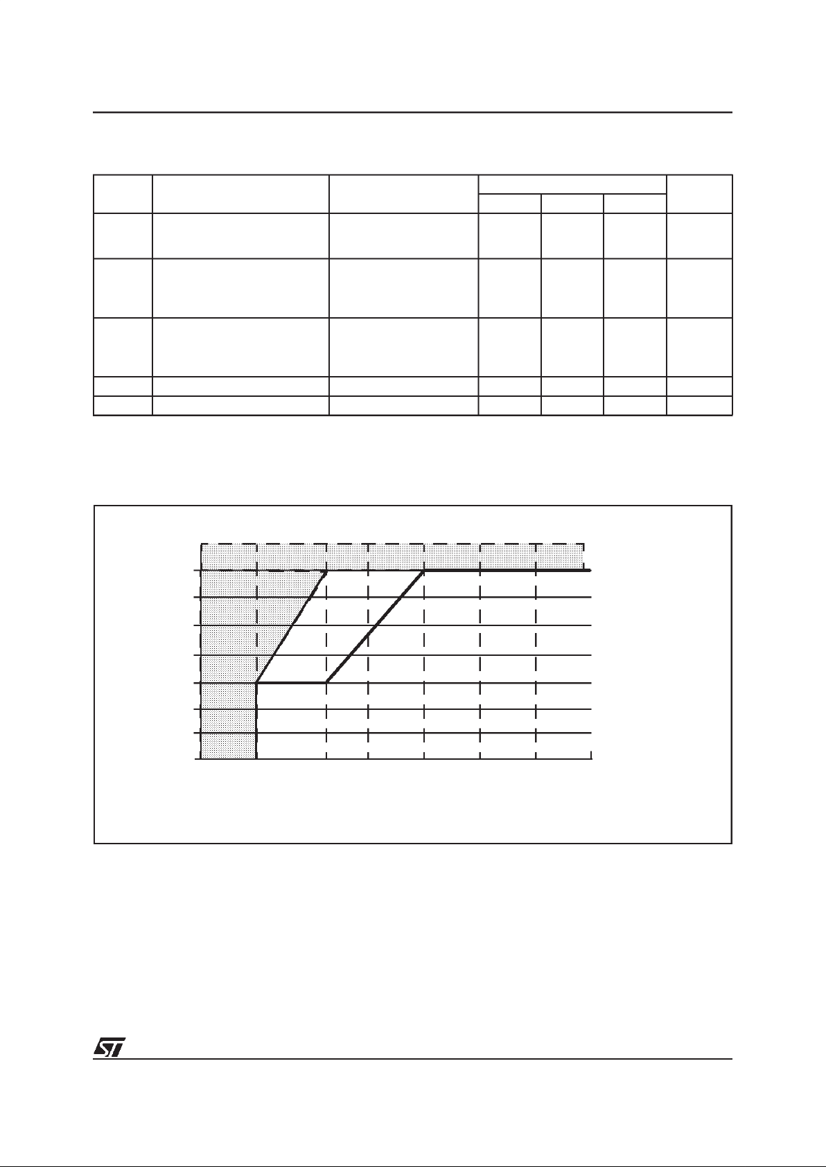
65/84
ST62T28C/E28C
6.2 RECOMMENDED OPERATING CONDITIONS
Notes:
1. Care must be taken in case ofnegative current injection, where adapted impedance must be respected onanalog sources to not affect the
A/D conversion. For a -1mA injection, a maximum 10 KΩ is recommended.
2.An oscillator frequency above 1MHz is recommended for reliable A/D results
Figure 35. Maximum Operating FREQUENCY (Fmax) Versus SUPPLY VOLTAGE (VDD)
The shaded area is outside the recommended operating range; device functionality is notguaranteed under these conditions.
Symbol Parameter Test Conditions
Value
Unit
Min. Typ. Max.
T
A
Operating Temperature
6 Suffix Version
1 Suffix Version
3 Suffix Version
-40
0
-40
85
70
125
°C
V
DD
Operating Supply Voltage
f
OSC
=4MHz, 1 & 6 Suffix
f
OSC
=4MHz, 3 Suffix
fosc= 8MHz , 1 & 6 Suffix
fosc= 8MHz , 3 Suffix
3.0
3.0
3.6
4.5
6.0
6.0
6.0
6.0
V
f
OSC
Oscillator Frequency
2)
VDD= 3.0V,1 & 6 Suffix
V
DD
= 3.0V , 3 Suffix
V
DD
= 3.6V , 1 & 6 Suffix
V
DD
= 3.6V , 3 Suffix
0
0
0
0
4.0
4.0
8.0
4.0
MHz
I
INJ+
Pin Injection Current (positive) VDD= 4.5 to 5.5V +5 mA
I
INJ-
Pin Injection Current (negative) VDD= 4.5 to 5.5V -5 mA
8
7
6
5
4
3
2
1
2.5 3 4 4.5 5 5.5 6
SUPPLY VOLTAGE (VDD)
Maximum FREQUENCY (MHz)
FUNCTIONALITY IS NOT
GUARANTEED IN
THIS AREA
3 Suffix version
1 & 6 Suffix version
3.6
65
Page 66
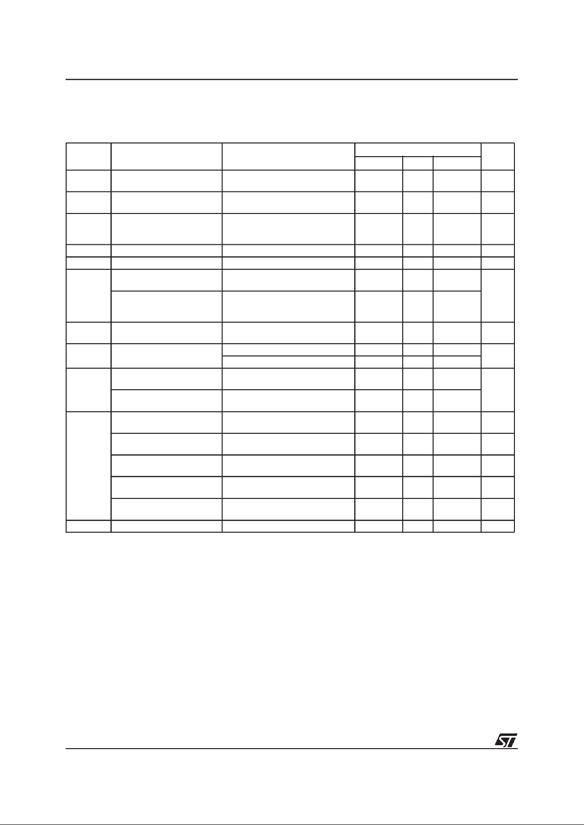
66/84
ST62T28C/E28C
6.3 DC ELECTRICAL CHARACTERISTICS
(TA= -40 to +125°C unless otherwise specified)
Notes:
(1) Hysteresis voltage between switching levels
(2) All peripherals running
(3) All peripherals in stand-by
Symbol Parameter Test Conditions
Value
Unit
Min. Typ. Max.
V
IL
Input Low Level Voltage
All Input pins
V
DD
x 0.3 V
V
IH
Input High LevelVoltage
All Input pins
V
DD
x 0.7 V
V
Hys
Hysteresis Voltage
(1)
All Input pins
V
DD
=5V
V
DD
=3V
0.2
0.2
V
V
up
LVD Threshold in power-on 4.1 4.3
V
dn
LVDthreshold in powerdown 3.5 3.8
V
OL
Low Level Output Voltage
All Output pins
VDD= 5.0V; IOL= +10µA
V
DD
= 5.0V; IOL= + 3mA
0.1
0.8
V
Low Level Output Voltage
20 mA Sink I/O pins
V
DD
= 5.0V; IOL= +10µA
V
DD
= 5.0V; IOL= +7mA
V
DD
= 5.0V; IOL= +15mA
0.1
0.8
1.3
V
OH
High Level Output Voltage
All Output pins
VDD= 5.0V; IOH= -10µA
V
DD
= 5.0V; IOH= -3.0mA
4.9
3.5
V
R
PU
Pull-up Resistance
All Input pins 40 100 350
ΚΩ
RESET pin 150 350 900
I
IL
I
IH
Input Leakage Current
All Input pins but RESET
VIN=VSS(No Pull-Up configured)
V
IN=VDD
0.1 1.0
µA
Input Leakage Current
RESET pin
V
IN=VSS
VIN=V
DD
-8 -16 -30
10
I
DD
Supply Current in RESET
Mode
V
RESET=VSS
f
OSC
=8MHz
7.0 mA
Supply Current in
RUN Mode
(2)
VDD=5.0V f
INT
=8MHz 7.0 mA
Supply Current in WAIT
Mode
(3)
VDD=5.0V f
INT
=8MHz 1.5 mA
Supply Current in STOP
Mode, with LVD disabled
(3)
I
LOAD
=0mA
V
DD
=5.0V
20 µA
Supply Current in STOP
Mode, with LVD enabled
(3)
I
LOAD
=0mA
V
DD
=5.0V
500
Retention EPROM Data Retention T
A
=55°C 10 years
66
Page 67

67/84
ST62T28C/E28C
DC ELECTRICAL CHARACTERISTICS (Cont’d)
(TA= -40 to +85°C unless otherwise specified))
Note:
(*) All Peripherals in stand-by.
6.4 AC ELECTRICAL CHARACTERISTICS
(TA= -40 to +125°C unless otherwise specified)
Notes:
1. Period for which V
DD
has to be connected at 0V to allow internal Reset function at next power-up.
2 An oscillator frequency above 1MHz is recommended for reliable A/D results.
3. Measure performed with OSCin pin soldered on PCB, with an around 2pF equivalent capacitance.
Symbol Parameter Test Conditions
Value
Unit
Min. Typ. Max.
V
up
LVD Threshold in power-on Vdn+50 mV 4.1 4.3 V
V
dn
LVDthreshold in powerdown 3.6 3.8 Vup-50 mV V
V
OL
Low Level Output Voltage
All Output pins
V
DD
= 5.0V; IOL= +10µA
V
DD
= 5.0V; IOL= + 5mA
V
DD
= 5.0V; IOL= + 10mAv
0.1
0.8
1.2
V
Low Level Output Voltage
20 mA Sink I/O pins
V
DD
= 5.0V; IOL= +10µA
V
DD
= 5.0V; IOL= +10mA
V
DD
= 5.0V; IOL= +20mA
V
DD
= 5.0V; IOL= +30mA
0.1
0.8
1.3
2.0
V
OH
High Level Output Voltage
All Output pins
VDD= 5.0V; IOH= -10µA
V
DD
= 5.0V; IOH= -5.0mA
4.9
3.5
V
I
DD
Supply Current in STOP
Mode, with LVD disabled
(*)
I
LOAD
=0mA
V
DD
=5.0V
10 µA
Symbol
Parameter Test Conditions
Value
Unit
Min. Typ. Max.
t
REC
Supply Recovery Time
(1)
100 ms
f
LFAO
Internal frequency with LFAO active 200 400 800 kHz
f
OSG
Internal Frequency with OSG
enabled
2)
VDD=3V
V
DD
= 3.6V
V
DD
= 4.5V
V
DD
=6V
1
1
2
2
f
OSC
MHz
f
RC
Internal frequency with RC oscillator
and OSG disabled
2) 3)
VDD=5.0V
R=47kΩ
R=100kΩ
R=470kΩ
4
2.7
800
5
3.2
850
5.8
3.5
900
MHz
MHz
kHz
C
IN
Input Capacitance All Inputs Pins 10 pF
C
OUT
Output Capacitance All Outputs Pins 10 pF
67
Page 68

68/84
ST62T28C/E28C
6.5 A/D CONVERTER CHARACTERISTICS
(TA= -40 to +125°C unless otherwise specified)
Notes:
1. Noise at VDD, VSS <10mV
2. With oscillator frequencies less than 1MHz, the A/D Converter accuracy is decreased.
6.6 TIMER CHARACTERISTICS
(TA= -40 to +125°C unless otherwise specified)
6.7 SPI CHARACTERISTICS
(TA= -40 to +125°C unless otherwise specified)
6.8 ARTIMER ELECTRICAL CHARACTERISTICS
(TA= -40 to +125°C unless otherwise specified)
Symbol Parameter Test Conditions
Value
Unit
Min. Typ. Max.
Res Resolution 8 Bit
A
TOT
TotalAccuracy
(1) (2)
f
OSC
> 1.2MHz
f
OSC
> 32kHz
±2
±4
LSB
t
C
Conversion Time
f
OSC
= 8MHz (TA<85°C)
f
OSC
= 4 MHz
70
140
µs
ZIR Zero Input Reading
Conversion result when
V
IN=VSS
00 Hex
FSR Full Scale Reading
Conversion result when
V
IN=VDD
FF Hex
AD
I
Analog Input CurrentDuring
Conversion
V
DD
= 4.5V 1.0 µA
AC
IN
Analog Input Capacitance 2 5 pF
Symbol Parameter Test Conditions
Value
Unit
Min. Typ. Max.
f
IN
Input Frequency on TIMER Pin MHz
t
W
Pulse Width at TIMER Pin
V
DD
= 3.0V
V
DD
>4.5V
1
125
µs
ns
IINT
4
----------
Page 69

69/84
ST62T28C/E28C
Figure 36.. RC frequency versus Vcc
Figure 37. LVD thresholds versus temperature
3 3.5 4 4.5 5 5.5 6
0.1
1
10
0
+
]
VDD (volts)
Frequency
R=47K
R=100K
R=470K
Page 70

70/84
ST62T28C/E28C
Figure 38. Idd WAIT versus Vcc at 8 Mhz for OTP devices
Figure 39. Idd STOP versus Vcc for OTP devices
Figure 40. Idd STOP versus Vcc for ROM devices
0
0.2
0.4
0.6
0.8
1
1.2
Vdd
Idd WAIT(mA)
3V 4V 5V 6V
T=-40°C
T=25°C
T=95°C
T = 125°C
This curves represents typical variations and is given for guidance only
-2
0
2
4
6
8
Vdd
Idd WAIT(µA)
3V 4V 5V 6V
T=-40°C
T=25°C
T=95°C
T = 125°C
This curves represents typical variations and is given for guidance only
-0.5
0
0.5
1
1.5
2
Vdd
Idd STOP (µA)
3V 4V 5V 6V
T = -40°C
T=25°C
T=95°C
T = 125°C
This curves represents typical variations and is given for guidance only
70
Page 71

71/84
ST62T28C/E28C
Figure 41. Idd WAIT versus Vcc at 8Mhz for ROM devices
Figure 42. Idd RUN versus Vcc at8 Mhz for ROM and OTP devices
Figure 43. Vol versus Iol on all I/O port at Vdd=5V
0
0.2
0.4
0.6
0.8
Vdd
Idd WAIT(mA)
3V 4V 5V 6V
T = -40°C
T=25°C
T=95°C
T = 125°C
This curves represents typical variations and is given for guidance only
0
2
4
6
8
Vdd
Idd RUN(mA)
3V 4V 5V 6V
T=-40°C
T=25°C
T=95°C
T= 125°C
This curves represents typical variations and is given for guidance only
010203040
0
2
4
6
8
Iol (mA)
Vol (V)
T=-40°C
T=25°C
T=95°C
T = 125°C
This curves represents typical variations and is givenfor guidance only
71
Page 72

72/84
ST62T28C/E28C
Figure 44. Vol versus Iol on all I/O port atT=25°C
Figure 45. Vol versus Iol for High sink (20mA) I/Oports at T=25°C
Figure 46. Vol versus Iol for High sink (20mA) I/O ports at Vdd=5V
010203040
0
2
4
6
8
Iol (mA)
Vol (V)
Vdd = 3.0V
Vdd = 4.0V
Vdd = 5.0V
Vdd = 6.0V
This curves represents typical variations and is givenfor guidance only
0 10203040
0
1
2
3
4
5
Iol (mA)
Vol (V)
Vdd = 3.0V
Vdd = 4.0V
Vdd = 5.0V
Vdd = 6.0V
0 10203040
0
1
2
3
4
5
Iol (mA)
Vol (V)
T = -40°C
T=25°C
T=95°C
T = 125°C
This curves represents typical variations and is given for guidance only
72
Page 73

73/84
ST62T28C/E28C
Figure 47. Voh versus Ioh on all I/O port at 25°C
Figure 48. Voh versus Ioh on all I/O port at Vdd=5V
0 10203040
-2
0
2
4
6
Ioh (mA)
Voh (V)
Vdd = 3.0V
Vdd = 4.0V
Vdd = 5.0V
Vdd = 6.0V
0 10203040
-2
0
2
4
6
Ioh (mA)
Voh (V)
T = -40°C
T=25°C
T=95°C
T = 125°C
This curves represents typical variations and is givenfor guidance only
73
Page 74

74/84
ST62T28C/E28C
7 GENERAL INFORMATION
7.1 PACKAGE MECHANICAL DATA
Figure 49. 28-Pin Plastic Dual In-Line Package, 600-mil Width
Figure 50. 28-Pin Ceramic Side-Brazed Dual In-Line Package
Dim.
mm inches
Min Typ Max Min Typ Max
A 6.35 0.250
A1 0.38 0.015
A2 3.18 4.95 0.125 0.195
B 0.36 0.56 0.014 0.022
B1 0.76 1.78 0.030 0.070
C 0.20 0.38 0.008 0.015
D 39.75 1.565
e 2.54 0.100
eA 15.24 0.600
E1 12.32 14.73 0.485 0.580
L 2.92 5.08 0.115 0.200
e3
e4
Number of Pins
N 28
PDIP28
Dim.
mm inches
Min Typ Max Min Typ Max
A 4.17 0.164
A1 0.76 0.030
B 0.36 0.46 0.56 0.014 0.018 0.022
B1 0.76 1.27 1.78 0.030 0.050 0.070
C 0.20 0.25 0.38 0.008 0.010 0.015
D 34.95 35.56 36.17 1.376 1.400 1.424
D1 33.02 1.300
E1 14.61 15.11 15.62 0.575 0.595 0.615
e 2.54 0.100
G 12.70 12.95 13.21 0.500 0.510 0.520
G1 12.70 12.95 13.21 0.500 0.510 0.520
G2 1.14 0.045
L 2.92 5.08 0.115 0.200
S 1.27 0.050
Ø 8.89 0.350
Number of Pins
N28
CDIP28W
74
Page 75
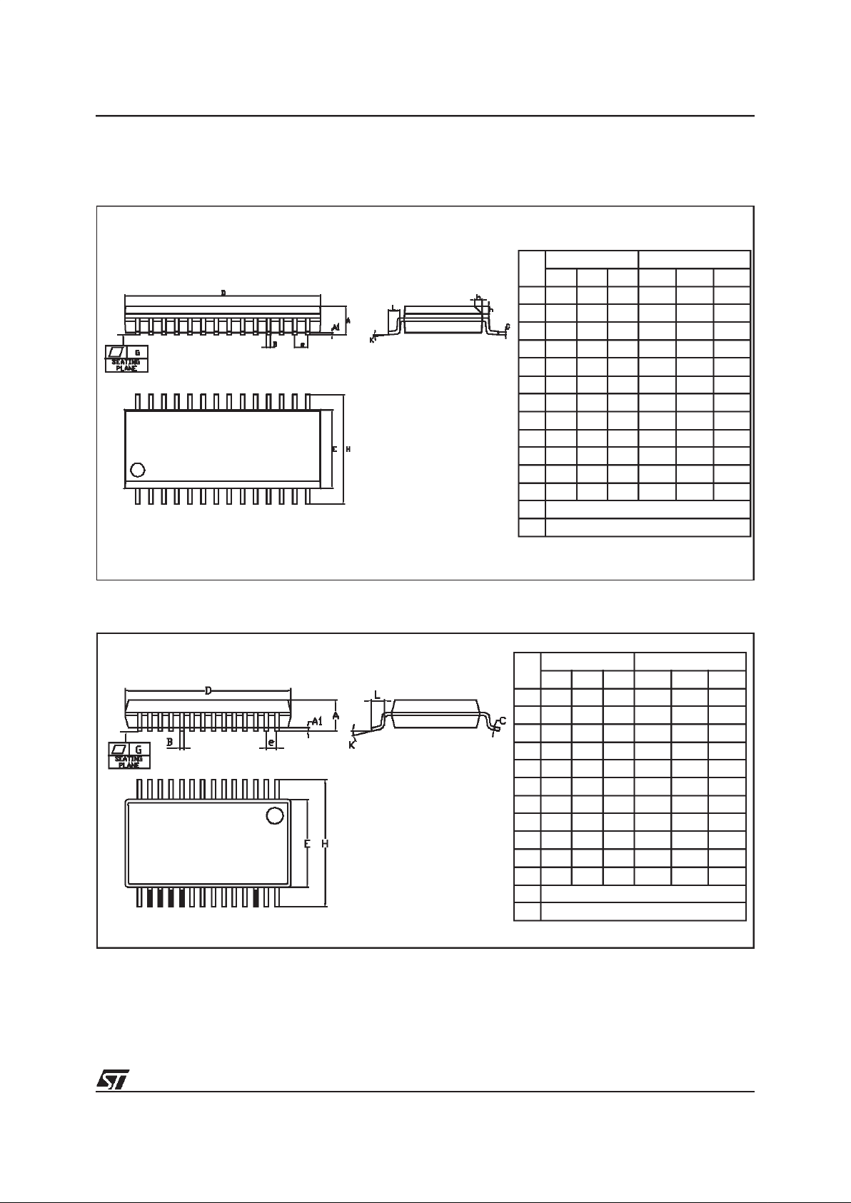
75/84
ST62T28C/E28C
PACKAGE MECHANICAL DATA (Cont’d)
Figure 51. 28-Pin Plastic Small Outline Package, 300-mil Width
Figure 52. 28-Pin Plastic Shrink Small Outline Package, 0.209” Width
Dim.
mm inches
Min Typ Max Min Typ Max
A 2.35 2.65 0.0926 0.1043
A1 0.10 0.30 0.0040 0.0118
B 0.33 0.51 0.013 0.020
C 0.23 0.32 0.0091 0.0125
D 17.70 18.10 0.6969 0.7125
E 7.40 7.60 0.2914 0.2992
e 1.27 0.0500
H 10.01 10.64 0.394 0.419
h 0.25 0.74 0.010 0.029
K 0° 8°
L 0.41 1.27 0.016 0.050
G 0.10 0.004
Number of Pins
N28
SO28
Dim.
mm inches
Min Typ Max Min Typ Max
A 1.73 1.86 1.99 0.068 0.073 0.078
A1 0.05 0.13 0.21 0.002 0.005 0.008
B 0.25 0.38 0.010 0.015
C 0.09 0.20 0.004 0.008
D 10.07 10.20 10.33 0.396 0.402 0.407
E 7.65 7.80 7.90 0.301 0.307 0.311
E1 5.20 5.30 5.38 0.205 0.209 0.212
e 0.65 0.026
G 0.076 0.003
K 0° 4° 8° 0° 4° 8°
L 0.63 0.75 0.95 0.025 0.030 0.037
Number of Pins
N28
SSOP28
75
Page 76

76/84
ST62T28C/E28C
THERMAL CHARACTERISTIC
7.2 ORDERING INFORMATION
Table 26. OTP/EPROM VERSION ORDERING INFORMATION
Symbol Parameter Test Conditions
Value
Unit
Min. Typ. Max.
RthJA Thermal Resistance
PDIP28 70
°C/W
PSO28 70
Sales Type
Program
Memory (Bytes)
I/O Temperature Range Package
ST62E28CF1 7948 (EPROM)
20
0to70°C CDIP28W
ST62T28CB6
7948 (OTP) -40 to85°C
PDIP28
ST62T28CM6 PSO28
ST62T28CN6 SSOP28
ST62T28CB3
7948 (OTP) -40 to +125°C
PDIP28
ST62T28CM3 PSO28
ST62T28CN3 SSOP28
76
Page 77

November 1999 77/84
Rev. 2.8
ST62P28C
8-BIT MCUs WITH A/D CONVERTER, AUTO-RELOAD
TIMER, UART, OSG, SAFE RESET AND 28-PIN PACKAGE
PRODUCT PREVIEW
■ 3.0 to 6.0V Supply Operating Range
■ 8 MHzMaximum Clock Frequency
■ -40 to+125°C Operating TemperatureRange
■ Run, Wait and Stop Modes
■ 5 InterruptVectors
■ Look-up Table capability in Program Memory
■ Data Storage in Program Memory:
User selectable size
■ Data RAM: 192 bytes
■ 20 I/O pins, fully programmable as:
– Input with pull-up resistor
– Input without pull-up resistor
– Input with interrupt generation
– Open-drain or push-pull output
– Analog Input
■ 8 I/Olines can sink up to 20mA todrive LEDs or
TRIACs directly
■ 8-bit Timer/Counter with 7-bit programmable
prescaler
■ 8-bit Auto-reload Timer with 7-bit programmable
prescaler (AR Timer)
■ Digital Watchdog
■ 8-bit A/D Converter with 12 analog inputs
■ 8-bit Asynchronous Peripheral Interface
(UART)
■ 8-bit Synchronous Peripheral Interface (SPI)
■ On-chip Clockoscillator can be driven by Quartz
Crystal, Ceramic resonator or RC Network
■ Oscillator SafeGuard
■ Low Voltage Detector for safe Reset
■ One external Non-Maskable Interrupt
■ ST623x-EMU2 Emulation and Development
System (connects to an MS-DOS PC via a
parallel port).
DEVICE SUMMARY
DEVICE
ROM
(Bytes)
I/O Pins
ST62P28C 7948 20
(See end of Datasheet for Ordering Information)
PDIP28
PS028
SS0P28
77
Page 78

78/84
ST62P28C
1 GENERAL DESCRIPTION
1.1 INTRODUCTION
The ST62P28C are the Factory Advanced Service
Technique ROM (FASTROM) versions of
ST62T18C OTPdevices.
They offer the same functionality as OTPdevices,
selecting as FASTROM options the options defined in the programmable option byte of the OTP
version.
1.2 ORDERING INFORMATION
The following section deals with the procedure for
transfer ofcustomer codes to STMicroelectronics.
1.2.1 Transfer of Customer Code
Customer code is made up of the ROM contents
and the list of the selected FASTROM options.
The ROM contents are to be sent on diskette, or
by electronic means, with the hexadecimal file
generated by the development tool. All unused
bytes mustbe set to FFh.
The selected options are communicated to STMicroelectronics using the correctly filled OPTION
LIST appended.
1.2.2 Listing Generation and Verification
When STMicroelectronics receives the user’s
ROM contents, a computer listing is generated
from it. This listing refers exactly to the ROM contents and options which will be used to produce
the specified MCU. The listing is then returned to
the customer who must thoroughly check, complete, sign and return it to STMicroelectronics. The
signed listingforms a part of the contractual agreement for the production of the specific customer
MCU.
The STMicroelectronics Sales Organization will be
pleased to provide detailed information on contractual points.
Table 1. ROM Memory Map for ST62P28C
Table 2. ROM version Ordering Information
(*) Advanced information
ROM Page Device Address Description
Page 0
0000h-007Fh
0080h-07FFh
Reserved
User ROM
Page 1
“STATIC”
0800h-0F9Fh
0FA0h-0FEFh
0FF0h-0FF7h
0FF8h-0FFBh
0FFCh-0FFDh
0FFEh-0FFFh
User ROM
Reserved
Interrupt Vectors
Reserved
NMI Vector
Reset Vector
Page 2
0000h-000Fh
0010h-07FFh
Reserved
User ROM
Page 3
0000h-000Fh
0010h-07FFh
Reserved
User ROM
Sales Type ROM I/O Temperature Range Package
ST62P28CB1/XXX
ST62P28CB6/XXX
ST62P28CB3/XXX(*)
7948 20
0 to+70°C
-40 to 85°C
-40 to + 125°C
PDIP28
ST62P28CM1/XXX
ST62P28CM6/XXX
ST62P28CM3/XXX(*)
0 to+70°C
-40 to 85°C
-40 to + 125°C
PSO28
ST62P28CN1/XXX
ST62P28CN6/XXX
ST62P28CN3/XXX(*)
0 to+70°C
-40 to 85°C
-40 to + 125°C
SSOP28
78
Page 79

79/84
ST62P28C
ST62P28C MICROCONTROLLER OPTION LIST
Customer . . . . . ..................................................
Address . . . . . ..................................................
Contact . . . . . ..................................................
Phone No . . . . . ..................................................
Reference .. . . . ..................................................
STMicroelectronics references
Device: [ ] ST62P28C
Package: [ ] Dual in Line Plastic
[ ]Small Outline Plastic
[ ] Tape & Reel [ ] Stick (Default)
[ ]Shrink Small Outline Plastic
Temperature Range: [ ] 0°Cto+70°C []-40°Cto+85°C[ ] - 40°Cto+125°C
Special Marking: [ ] No [ ] Yes ”_ _ __ _______”
Authorized characters are letters, digits, ’.’,’-’, ’/’and spaces only.
Maximum character count: PDIP28:10
PSO28: 8
Oscillator Source Selection: [ ] Crystal Quartz/Ceramic resonator
[ ]RC Network
Watchdog Selection: [ ] Software Activation
[ ]Hardware Activation
Ports Pull-Up Selection: [ ] Yes [ ] No
NMI Pull-Up Selection: [ ] Yes [ ] No
Timer Pull-Up Selection: [ ] Yes [ ] No
External STOP Mode Control: [ ] Enabled [ ] Disabled
OSG: [ ] Enabled [ ] Disabled
ROM Readout Protection: [ ]Standard (Fuse cannot be blown)
[ ]Enabled (Fuse can be blown by the customer)
Note: No part is delivered with protectedROM.
The fuse must be blown for protection to be effective.
Comments :
Supply Operating Range in the application:
Oscillator Fequency in the application:
Notes . . . . . ....................
Signature . . . . . ....................
Date . . . . . ....................
79
Page 80

80/84
ST62P28C
Notes:
80
Page 81

November 1999 81/84
Rev. 2.8
ST6228C
8-BIT MCUs WITH A/D CONVERTER, AUTO-RELOAD
TIMER, UART, OSG, SAFE RESET AND 28-PIN PACKAGE
PRODUCT PREVIEW
■ 3.0 to 6.0V Supply Operating Range
■ 8 MHzMaximum Clock Frequency
■ -40 to+125°C Operating TemperatureRange
■ Run, Wait and Stop Modes
■ 5 InterruptVectors
■ Look-up Table capability in Program Memory
■ Data Storage in Program Memory:
User selectable size
■ Data RAM: 192 bytes
■ 20 I/O pins, fully programmable as:
– Input with pull-up resistor
– Input without pull-up resistor
– Input with interrupt generation
– Open-drain or push-pull output
– Analog Input
■ 8 I/Olines can sink up to 20mA todrive LEDs or
TRIACs directly
■ 8-bit Timer/Counter with 7-bit programmable
prescaler
■ 8-bit Auto-reload Timer with 7-bit programmable
prescaler (AR Timer)
■ Digital Watchdog
■ 8-bit A/D Converter with 12 analog inputs
■ 8-bit Asynchronous Peripheral Interface
(UART)
■ 8-bit Synchronous Peripheral Interface (SPI)
■ On-chip Clockoscillator can be driven by Quartz
Crystal, Ceramic resonator or RC Network
■ Oscillator SafeGuard
■ Low Voltage Detector for safe Reset
■ One external Non-Maskable Interrupt
■ ST623x-EMU2 Emulation and Development
System (connects to an MS-DOS PC via a
parallel port).
DEVICE SUMMARY
DEVICE
ROM
(Bytes)
I/O Pins
ST6228C 7948 20
(See end of Datasheet for Ordering Information)
PDIP28
PS028
SS0P28
81
Page 82

82/84
ST6228C
1 GENERAL DESCRIPTION
1.1 INTRODUCTION
The ST6228C is mask programmed ROM version
of ST62T28C OTP devices.
They offer the same functionality as OTPdevices,
selecting as ROM options the options defined in
the programmableoption byte of the OTP version.
Figure 1. Programming wave form
1.2 ROM READOUT PROTECTION
If the ROM READOUT PROTECTION option is
selected, a protection fuse can be blown to prevent any access to theprogram memory content.
In case the user wants to blow this fuse, highvoltage must be applied onthe TEST pin.
Figure 2. Programming Circuit
Note: ZPD15 is used for overvoltage protection
0.5s min
TEST
15
14V typ
10
5
TEST
100mA
4mA typ
VR02001
max
150 µstyp
t
VR02003
TEST
5V
100nF
47mF
PROTECT
100nF
V
DD
V
SS
ZPD15
15V
14V
82
Page 83

83/84
ST6228C
ST6228C MICROCONTROLLER OPTIONLIST
Customer . . . . . ..................................................
Address . . . . . ..................................................
Contact . . . . . ..................................................
Phone No . . . . . ..................................................
Reference .. . . . ..................................................
STMicroelectronics references
Device: [ ] ST6228C
Package: [ ] Dual in Line Plastic
[ ]Small Outline Plastic
[ ] Tape & Reel [ ] Stick (Default)
[ ]Shrink Small Outline Plastic
Temperature Range: [ ] 0°Cto+70°C []-40°Cto+85°C[ ] - 40°Cto+125°C
Special Marking: [ ] No [ ] Yes ”_ _ __ _______”
Authorized characters are letters, digits, ’.’,’-’, ’/’and spaces only.
Maximum character count: PDIP28:10
PSO28: 8
Oscillator Source Selection: [ ] Crystal Quartz/Ceramic resonator
[ ]RC Network
Watchdog Selection: [ ] Software Activation
[ ]Hardware Activation
Ports Pull-Up Selection: [ ] Yes [ ] No
NMI Pull-Up Selection: [ ] Yes [ ] No
Timer Pull-Up Selection: [ ] Yes [ ] No
External STOP Mode Control: [ ] Enabled [ ] Disabled
OSG: [ ] Enabled [ ] Disabled
ROM Readout Protection: [ ]Standard (Fuse cannot be blown)
[ ]Enabled (Fuse can be blown by the customer)
Note: No part is delivered with protectedROM.
The fuse must be blown for protection to be effective.
Comments :
Supply Operating Range in the application:
Oscillator Fequency in the application:
Notes . . . . . ....................
Signature . . . . . ....................
Date . . . . . ....................
83
Page 84

84/84
ST6228C
1.3 ORDERING INFORMATION
The following section deals with the procedure for
transfer ofcustomer codes to STMicroelectronics.
1.3.1 Transfer of Customer Code
Customer code is made up of the ROM contents
and the list of the selected mask options. The
ROM contents are to be sent on diskette, or by
electronic means, withthe hexadecimalfile generated by the development tool. All unused bytes
must be set to FFh.
The selected mask options are communicated to
STMicroelectronics using the correctly filled OPTION LIST appended.
1.3.2 Listing Generation and Verification
When STMicroelectronics receives the user’s
ROM contents, a computer listing is generated
from it. This listing refersexactly to the mask which
will be used to produce the specified MCU. The
listing is then returned to the customer who must
thoroughly check, complete, sign and return it to
STMicroelectronics. The signed listing forms a
part of the contractual agreement for the creation
of the specific customer mask.
The STMicroelectronics Sales Organization will be
pleased to provide detailed information on contractual points.
Table 1. ROM Memory Map for ST6228C
Table 2. ROM version Ordering Information
Information furnished is believed to be accurate and reliable. However, STMicroelectronics assumes no responsibility for the consequences
of useof such information nor for any infringement of patents or other rights of third parties which may result from itsuse. No license isgranted
by implication or otherwise under any patent or patent rights of STMicroelectronics. Specifications mentioned in this publication are subject
to change without notice. This publication supersedes and replaces all information previously supplied. STMicroelectronics products are not
authorized for use as critical components in life support devices or systems without the express written approval of STMicroelectronics.
The ST logo is a registered trademark of STMicroelectronics
1999 STMicroelectronics - All Rights Reserved.
Purchase of I
2
C Components by STMicroelectronics conveys alicense under the Philips I2C Patent. Rights to use these components in an
I
2
C system is granted provided that the system conforms to the I2C Standard Specification asdefined by Philips.
STMicroelectronics Group of Companies
Australia - Brazil - China - Finland - France - Germany - Hong Kong - India - Italy - Japan - Malaysia - Malta - Morocco - Singapore - Spain
Sweden - Switzerland - United Kingdom - U.S.A.
http://www.st.com
ROM Page Device Address Description
Page 0
0000h-007Fh
0080h-07FFh
Reserved
User ROM
Page 1
“STATIC”
0800h-0F9Fh
0FA0h-0FEFh
0FF0h-0FF7h
0FF8h-0FFBh
0FFCh-0FFDh
0FFEh-0FFFh
User ROM
Reserved
Interrupt Vectors
Reserved
NMI Vector
Reset Vector
Page 2
0000h-000Fh
0010h-07FFh
Reserved
User ROM
Page 3
0000h-000Fh
0010h-07FFh
Reserved
User ROM
Sales Type ROM I/O Temperature Range Package
ST6228CB1/XXX
ST6228CB6/XXX
ST6228CB3/XXX
7948 20
0 to+70°C
-40 to 85°C
-40 to + 125°C
PDIP28
ST6228CM1/XXX
ST6228CM6/XXX
ST6228CM3/XXX
0 to+70°C
-40 to 85°C
-40 to + 125°C
PSO28
ST6228CN1/XXX
ST6228CN6/XXX
ST6228CN3/XXX
0 to+70°C
-40 to 85°C
-40 to + 125°C
SSOP28
84
 Loading...