

Datasheet ST62T03CM6, ST62T03CB6, ST62T01CM6, ST62T01CM3, ST62T01CB6 Datasheet (SGS Thomson Microelectronics)
...Page 1
August 1999 1/70
Rev. 2.8
ST62T00C/T01C
ST62T03C/E01C
8-BIT OTP/EPROM MCUs WITH A/D CONVERTER,
OSCILLATOR SAFEGUARD, SAFE RESET AND 16 PINS
■ 3.0 to 6.0V Supply Operating Range
■ 8 MHzMaximum Clock Frequency
■ -40 to +125°C Operating Temperature Range
■ Run, Wait and Stop Modes
■ 5 InterruptVectors
■ Look-up Table capability in Program Memory
■ Data Storage in Program Memory:
User selectable size
■ Data RAM: 64bytes
■ User Programmable Options
■ 9 I/O pins, fully programmable as:
– Input with pull-up resistor
– Input without pull-up resistor
– Input with interrupt generation
– Open-drain or push-pull output
– Analog Input (except ST62T03C)
■ 3I/O lines can sink up to 20mA to drive LEDs or
TRIACs directly
■ 8-bit Timer/Counter with 7-bit programmable
prescaler
■ Digital Watchdog
■ Oscillator Safe Guard
■ Low Voltage Detector for Safe Reset
■ 8-bit A/D Converter with up to 4 analog inputs
■ On-chip Clockoscillator canbedrivenbyQuartz
Crystal Ceramic resonator or RC network
■ Power-on Reset
■ One external Non-Maskable Interrupt
■ ST626x-EMU2 Emulation and Development
System (connects to an MS-DOS PC via a
parallel port)
DEVICE SUMMARY
DEVICE
OTP
(Bytes)
EPROM
(Bytes)
I/O Pins
Analog
inputs
ST62T00C 1036 - 9 4
ST62T01C 1836 - 9 4
ST62T03C 1036 - 9 None
ST62E01C - 1836 9 4
(See end of Datasheet for Ordering Information)
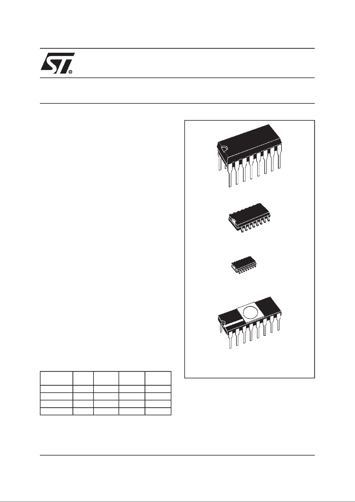
PDIP16
PSO16
CDIP16W
SSOP16
1
Page 2

2/70
Table of Contents
70
Document
Page
2
ST62T00C/T01C/ST62T03C/E01C . . . . . . . . . . . . . . . . . . . . . . . 1
1 GENERAL DESCRIPTION . . . . . . ................................................ 4
1.1 INTRODUCTION . . . . . .. . . . . . . ............................................ 4
1.2 PIN DESCRIPTIONS . . . . . . ................................................5
1.3 MEMORY MAP . . . . . . . . . . ................................................ 6
1.3.1 Introduction . . . ..................................................... 6
1.3.2 Program Space . . . . . . . . . . . . . . . . . . . . .................................7
1.3.3 Data Space . . . . . . . . . . . . . . . . . . . . . . . . . ............................... 8
1.3.4 Stack Space . . . . .. . . . . . . ............................................ 8
1.3.5 Data Window Register (DWR) . ......................................... 9
1.4 PROGRAMMING MODES . . . . . . . . . . . . . . . . . . . . . . . . . . . . . . . . . . . . . . . . . . . . . . . . . 10
1.4.1 Option Bytes .. .. . . . . . . . . . . . . . . . . . . . ............................... 10
1.4.2 Program Memory . . . ................................................ 11
1.4.3 EPROM Erasing .................................................... 11
2 CENTRAL PROCESSING UNIT . . ............................................... 12
2.1 INTRODUCTION . . . . . .. . . . . . . ...........................................12
2.2 CPU REGISTERS . . . .................................................... 12
3 CLOCKS, RESET, INTERRUPTS AND POWER SAVING MODES . . ................... 14
3.1 CLOCK SYSTEM . . . . . . . . . . . . . ........................................... 14
3.1.1 Main Oscillator . . . . . . . . . . . . . . . . . . . . ................................. 14
3.1.2 Low Frequency Auxiliary Oscillator (LFAO) . . . . . . . . . . . . . . . . . . . . . . . . . . . . . . . 15
3.1.3 Oscillator Safe Guard . . . . . ........................................... 15
3.2 RESETS . . . . . . . . . . . . . . . . . . . . . . . . . . . . . . . . . . . . . . . . . . . . . . . . . . . . . . . . . . . . . . . 18
3.2.1 RESET Input . . .................................................... 18
3.2.2 Power-on Reset .................................................... 18
3.2.3 Watchdog Reset . . . . . . . . . . . . . . . . . . ................................. 19
3.2.4 LVD Reset . . . . . . . . . ...............................................19
3.2.5 Application Notes . . . ................................................ 19
3.2.6 MCU Initialization Sequence . . . . . . . . .................................. 20
3.3 DIGITAL WATCHDOG . . . . . . . . . . . . . . . . . . .................................. 22
3.3.1 Digital Watchdog Register (DWDR) . . . . . . . . . . . . . . . . . . . . . . . . . . . . . . . . . . . . . 24
3.3.2 Application Notes . . . ................................................ 24
3.4 INTERRUPTS . . . . . . . . . . . . . . . . . . . . . . . . . . . . . . . . . . . . . . . . . . . . . . . . . . . . . . . . . . 26
3.4.1 Interrupt request . ................................................... 26
3.4.2 Interrupt Procedure . . . . . . . . . . . . . . . . ................................. 27
3.4.3 Interrupt Option Register (IOR) . . . . . . . . . . . . . . . . . . . . . . . . . ............... 28
3.4.4 Interrupt sources . . . . . . . . . . . ........................................28
3.5 POWER SAVING MODES . . . . . . . . . . . . . . . . . . . . . . . . . . . . . . . . . . . . . . . . . ........ 30
3.5.1 WAIT Mode ....................................................... 30
3.5.2 STOP Mode . . . . . . . . ...............................................30
3.5.3 Exit from WAIT and STOP Modes . . . . ..................................31
4 ON-CHIP PERIPHERALS . . . . . . . . . . . ........................................... 32
4.1 I/O PORTS . . . . . . . . . . . . . . . . . . ...........................................32
4.1.1 Operating Modes . . . . . . . . . . . . . . . . . . . . . . . . ........................... 33
4.1.2 Safe I/O State Switching Sequence . . . . . . . . . . . . . . . . . . . . . . . . . . . . . . . . . . . . . 34
4.1.3 I/O Port Option Registers . . . . . . . . . . . .................................. 35
Page 3

3/70
Table of Contents
Document
Page
3
4.1.4 I/O Port Data Direction Registers . . . . . . . . . . . . . . . . . . . .. . . . . . . . . . . . . . . . . . . 35
4.1.5 I/O Port Data Registers . . . . . . ........................................ 35
4.2 TIMER . . . . . . . . . . . . . . . . . . . . . . . . . . . . . . . ................................. 37
4.2.1 Timer Operation . . . . . . . . . . . . . . .. . . . . . . .............................. 38
4.2.2 Timer Interrupt . . . . . . . . . . . . . . . . . . . . ................................. 38
4.2.3 Application Notes . . . ................................................ 38
4.2.4 Timer Registers . . . . . ............................................... 39
4.3 A/D CONVERTER (ADC) . . ............................................... 40
4.3.1 Application Notes . . . ................................................ 40
5 SOFTWARE . . . . . . . . . . . . . . . . . ............................................... 42
5.1 ST6 ARCHITECTURE . ................................................... 42
5.2 ADDRESSING MODES . . . . . . . . . . . . . . . . . .................................. 42
5.3 INSTRUCTION SET . . . . . . . ............................................... 43
6 ELECTRICAL CHARACTERISTICS . . . . . . . . . . . . . . . . .............................. 48
6.1 ABSOLUTE MAXIMUM RATINGS . . . ........................................ 48
6.2 RECOMMENDED OPERATING CONDITIONS .. . .............................. 49
6.3 DC ELECTRICAL CHARACTERISTICS . . . . . . . . . . . . . . . . . . . . . . . . . . . ........... 50
6.4 AC ELECTRICAL CHARACTERISTICS . . . . . . . . . . . . . . . . . . . . . . . . . . . . . . . . . . . . . . 51
6.5 A/D CONVERTER CHARACTERISTICS . . . . . . . . . . . . . . . . . . . . . . . . . . . . . . . . . . . . . . 52
6.6 TIMER CHARACTERISTICS . . . . ........................................... 52
7 GENERAL INFORMATION . . . . . . . . . . ...........................................58
7.1 PACKAGE MECHANICAL DATA . . . . . . . . . . . . . . . . . ........................... 58
7.2 ORDERING INFORMATION . . . . . . . . . . . . . .................................. 60
ST62P00C/P01C/P03C . . . . ...........................61
1 GENERAL DESCRIPTION . . . . . . ............................................... 62
1.1 INTRODUCTION . . . . . .. . . . . . . ...........................................62
1.2 ORDERING INFORMATION . . . . . . . . . . . . . .................................. 62
1.2.1 Transfer of Customer Code . . . . . . . . . . ................................. 62
1.2.2 Listing Generation and Verification . . . . ................................. 62
ST6200C/01C/03C ...................................65
1 GENERAL DESCRIPTION . . . . . . ............................................... 66
1.1 INTRODUCTION . . . . . .. . . . . . . ...........................................66
1.2 ROM READOUT PROTECTION . . . . . . . . . . . .................................66
1.3 ORDERING INFORMATION . . . . . . . . . . . . . .................................. 68
1.3.1 Transfer of Customer Code . . . . . . . . . . ................................. 68
1.3.2 Listing Generation and Verification . . . . ................................. 68
Page 4

4/70
ST62T00C/T01C ST62T03C/E01C
1 GENERAL DESCRIPTION
1.1 INTRODUCTION
The ST62T00C,T01C,T03C and ST62E01C devices are low cost members of the ST62xx 8-bit
HCMOS familyofmicrocontrollers,which is targeted at low to medium complexity applications. All
ST62xx devices are based on a building block approach: a common core is surrounded by a
number of on-chip peripherals.
The ST62E01C isthe erasable EPROM versionof
the ST62T00C,T01C,T03C and device, which
may be used to emulate the ST62T00C,T01C and
T03C device, as well as the respective
ST6200C,01C and 03C ROM devices.
OTP and EPROM devices are functionally identical. TheROM based versions offer the same functionality selecting as ROM options the options de-
fined in the programmable option bytes of the
OTP/EPROM versions.
OTP devices offer all the advantages of user programmability at low cost, which make them the
ideal choice in a wide range of applications where
frequent code changes, multiple code versions or
last minute programmability are required.
These compact low-cost devices feature a Timer
comprising an 8-bit counter and a 7-bit programmable prescaler,an 8-bit A/D Converter with up to
4 analog inputs and a Digital Watchdog timer,
making them well suited for a wide range of automotive, appliance and industrial applications.
Figure 1. Block Diagram
TEST
NMI
INTERRUPT
PROGRAM
1836 Bytes
PC
STACK LEVEL 1
STACK LEVEL 2
STACK LEVEL 3
STACK LEVEL 4
STACK LEVEL 5
STACK LEVEL 6
POWER
SUPPLY
OSCILLATOR
RESET
DATA ROM
USER
SELECTABLE
DATA RAM
64 Bytes
PORT A
PORT B
TIMER
DIGITAL
8 BIT CORE
TEST/V
PP
(ST62T01C, E01C)
8-BIT
A/D CONVERTER
PA1..PA3 (20mA Sink)
V
DDVSS
OSCin OSCout RESET
WATCHDOG
:
MEMORY
PB0..PB1
1036 Bytes
(ST62T00C,T03C)
(*) Analog input availability depend on versions
PB3,PB5..PB7 / Ain (*)
4
Page 5

5/70
ST62T00C/T01C ST62T03C/E01C
1.2 PIN DESCRIPTIONS
VDDand VSS. Power is supplied to the MCU via
these two pins. VDDis the power connection and
VSSis the ground connection.
OSCin and OSCout. These pins are internally
connected totheon-chip oscillator circuit. Aquartz
crystal, a ceramic resonator or an external clock
signal can be connected between these two pins.
The OSCin pin is the input pin, the OSCout pin is
the output pin.
RESET. The active-low RESET pin is used to restart the microcontroller. Internal pull-up is provided at this pin.
TEST/VPP. The TEST must be held at VSSfor nor-
mal operation. If TEST pin is connected to a
+12.5V level during the reset phase, the EPROM
programming Mode is entered.
NMI. TheNMI pin provides the capability for asynchronous interruption, by applying an external non
maskable interrupt to the MCU. The NMI input is
falling edge sensitive. The user can select as option the availability of an on-chip pull-up at this pin.
PA1-PA3. These 3 lines are organized as one I/O
port (A). Each line may be configured under software controlas inputs with or without internal pullup resistors, interrupt generating inputs with pullup resistors,open-drainorpush-pull outputs. PA1PA3 can also sink 20mA for direct LED driving.
PB0..PB1,PB3,PB5-PB7. These 6 lines are organized as one I/O port (B). Each line may be configured under software control as inputs with or
without internal pull-up resistors, interrupt generating inputs with pull-up resistors, open-drain or
push-pull outputs. PB3,PB5..-PB7 can be used as
analog inputs for the A/D converter on the
ST62T00C, T01C and E01C.
Figure 2. ST62T03C,T00C, T01C, and E01C Pin
Configuration
1
2
3
4
5
6
7
8
11
12
13
14
15
16
V
DD
OSCin
OSCout
NMI
V
PP
/TEST
RESET
Ain*/PB7
Ain*/PB6
V
SS
PA1/20 mA Sink
PA2/20 mA Sink
PA3/20 mA Sink
PB0
PB1
PB3/Ain*
PB5/Ain*
*Analog input availability depend on device
10
9
5
Page 6

6/70
ST62T00C/T01C ST62T03C/E01C
1.3 MEMORY MAP
1.3.1 Introduction
The MCU operates in three separate memory
spaces: Program space, Data space, and Stack
space. Operationin these three memory spaces is
described in the following paragraphs.
Briefly, Program space contains user program
code in OTP and user vectors; Data space contains user data in RAM and in OTP, and Stack
space accommodates six levels of stack for subroutine and interrupt service routine nesting.
Figure 3. Memory Addressing Diagram
PROGRAM SPACE
PROGRAM
INTERRUPT &
RESET VECTORS
ACCUMULATOR
DATA RAM
BANK SELECT
WINDOW SELECT
RAM
X REGISTER
Y REGISTER
V REGISTER
W REGISTER
DATA READ-ONLY
WINDOW
RAM / EEPROM
BANKING AREA
000h
03Fh
040h
07Fh
080h
081h
082h
083h
084h
0C0h
0FFh
0-63
DATA SPACE
0000h
0FF0h
0FFFh
MEMORY
MEMORY
DATA READ-ONLY
MEMORY
6
Page 7

7/70
ST62T00C/T01C ST62T03C/E01C
MEMORY MAP (Cont’d)
1.3.2 Program Space
Program Space comprises the instructions to be
executed, the data required for immediate addressing mode instructions, the reserved factory
test area and the user vectors. Program Space is
addressed via the 12-bit ProgramCounter register
(PC register)Program Memory Protection.
The Program Memory in OTP or EPROM devices
can beprotectedagainstexternal readoutof memory by selecting the READOUT PROTECTION option in theoption byte.
In the EPROM parts, READOUT PROTECTION
option can be disactivated only by U.V. erasure
that also results into the whole EPROM context
erasure.
Note: Once the Readout Protection is activated, it
is no longer possible, evenfor STMicroelectronics,
to gain access to the OTP contents. Returned
parts witha protection setcan therefore not be accepted.
Figure 4. Program Memory Map
(*) Reserved areas should be filled with 0FFh
0000h
0AFFh
0B00h
0B9Fh
NOT IMPLEMENTED
RESERVED
*
USER
PROGRAM MEMORY
(OTP)
1024 BYTES
0BA0h
0F9Fh
0FA0h
0FEFh
0FF0h
0FF7h
0FF8h
0FFBh
0FFCh
0FFDh
0FFEh
0FFFh
RESERVED
*
RESERVED
INTERRUPT VECTORS
NMI VECTOR
USER RESET VECTOR
0000h
07FFh
0800h
087Fh
NOT IMPLEMENTED
RESERVED
*
USER
PROGRAM MEMORY
(OTP/EPROM)
1824 BYTES
0880h
0F9Fh
0FA0h
0FEFh
0FF0h
0FF7h
0FF8h
0FFBh
0FFCh
0FFDh
0FFEh
0FFFh
RESERVED
*
RESERVED
INTERRUPT VECTORS
NMI VECTOR
USER RESET VECTOR
ST62T03C,T00C ST62T01C, E01C
7
Page 8

8/70
ST62T00C/T01C ST62T03C/E01C
MEMORY MAP (Cont’d)
1.3.3 Data Space
Data Space accommodatesall the datanecessary
for processing the user program. This space comprises the RAM resource, the processor core and
peripheral registers, as well as read-only data
such as constants and look-up tables in OTP/
EPROM.
1.3.3.1 Data ROM
All read-only data is physically stored in program
memory, which also accommodates the Program
Space. The program memory consequently contains the program code to be executed, as well as
the constants and look-up tables required by the
application.
The Data Space locations in which the different
constants andlook-up tables are addressed by the
processor core may be thought of as a 64-byte
window through which it is possible to access the
read-only data stored in OTP/EPROM.
1.3.3.2 Data RAM
In ST6200C/01C/03C devices, the data space includes 60 bytes of RAM, the accumulator (A), the
indirect registers (X), (Y), the short direct registers
(V), (W), the I/O port registers, the peripheral data
and control registers, the interrupt option register
and the Data ROM Window register (DRW register).
1.3.4 Stack Space
Stack space consists of six 12-bit registers which
are used to stack subroutine and interrupt return
addresses, as well as the current program counter
contents.
Table 1. ST6200C/01C/03C Data Memory Space
RESERVED
000h
03Fh
DATA ROM WINDOW AREA
64 BYTES
040h
07Fh
X REGISTER 080h
Y REGISTER 081h
V REGISTER 082h
W REGISTER 083h
DATA RAM 60 BYTES
084h
0BFh
PORT A DATA REGISTE R 0C0h
PORT B DATA REGISTE R 0C1h
RESERVED 0C2h
RESERVED 0C3h
PORT A DIRECTION REGISTER 0C4h
PORT B DIRECTION REGISTER 0C5h
RESERVED 0C6h
RESERVED 0C7h
INTERRUPT OPTION REGISTER 0C8h*
DATA ROM WINDOW REGISTER 0C9h*
RESERVED
0CAh
0CBh
PORT A OPTION REGISTER 0CCh
PORT B OPTION REGISTER 0CDh
RESERVED 0CEh
RESERVED 0CFh
A/D DATA REGISTER(except ST62T03C) 0D0h
A/D CONTROL REGISTER (except ST62T03C) 0D1h
TIMER PRESCALER REGISTER 0D2h
TIMER COUNTER REGISTER 0D3h
TIMER STATUS CONTROL REGISTER 0D4h
RESERVED
0D5h
0D6h
0D7h
WATCHDOG REGISTER 0D8h
RESERVED
0D9h
0FEh
ACCUMULATOR 0FFh
* WRITE ONLY REGISTER
8
Page 9

9/70
ST62T00C/T01C ST62T03C/E01C
MEMORY MAP (Cont’d)
1.3.5 Data Window Register (DWR)
TheDataread-only memorywindowislocatedfrom
address 0040h to address 007Fh in Data space. It
allows direct reading of64consecutive byteslocated anywhere in program memory, between address 0000h and 0FFFh (top memory address depends on the specific device). All the program
memory can therefore be used to store either instructions or read-only data. Indeed, the window
can be moved in steps of 64 bytes along the program memorybywriting theappropriatecode in the
Data Window Register (DWR).
The DWR can beaddressed like any RAM location
in the Data Space,it is however a write-only register and therefore cannot be accessedusing singlebit operations. This register is used to position the
64-byte read-only data window (from address 40h
to address 7Fh of the Data space) in program
memory in 64-byte steps. The effective address of
the byte to be read as data in program memory is
obtained by concatenating the 6 least significant
bits of the register address given in the instruction
(as least significant bits) and the content of the
DWR register(asmostsignificant bits), as illustrated in Figure 5 below. Forinstance, when addressing location 0040h of the Data Space, with 0 loaded in the DWR register, the physical location addressed inprogram memory is 00h. The DWRregister is not cleared on reset, therefore it must be
written to prior to the first access to the Data readonly memory window area.
Data Window Register (DWR)
Address: 0C9h — Write Only
Bits 6, 7 = Not used.
Bit 5-0 = DWR5-DWR0:
Data read-only memory
Window Register Bits.
These are the Data readonly memory Window bits that correspond to the
upper bits of the data read-only memory space.
Caution:
This register is undefined on reset. Neither read norsingle bit instructionsmay be used to
address this register.
Note: Care is required when handling the DWR
register as it is write only. For this reason, the
DWR contents should not be changed while executing an interrupt service routine, as the service
routine cannot saveand then restore the register’s
previous contents. If it is impossible to avoid writing to the DWR during theinterruptserviceroutine,
an image of the register must be saved in a RAM
location, and each time the program writes to the
DWR, it must also write to the image register. The
image register must be written first so that, if an interrupt occurs between the two instructions, the
DWR is not affected.
Figure 5. Data read-only memory Window Memory Addressing
70
- - DWR5 DWR4 DWR3 DWR2 DWR1 DWR0
DATA ROM
WINDOW REGISTER
CONTENTS
DATA SPACE ADDRESS
40h-7Fh
IN INSTRUCTION
PROGRAM SPACE ADDRESS
765432 0
543210
543210
READ
1
67891011
0
1
VR01573C
12
1
0
DATA SPACE ADDRESS
:
:
59h
000
0
1
00
1
11
Example:
(DWR)
DWR=28h
1100000001
ROM
ADDRESS:A19h
11
13
0
1
9
Page 10

10/70
ST62T00C/T01C ST62T03C/E01C
1.4 PROGRAMMING MODES
1.4.1 Option Bytes
The two Option Bytes allow configuration capability to the MCUs. Option byte’s content is automatically read, and the selected options enabled,when
the chip reset is activated.
It can only be accessed during the programming
mode. This access is made either automatically
(copy from a master device) or by selecting the
OPTION BYTE PROGRAMMING modeof the programmer.
The option bytes are located in a non-user map.
No address hasto be specified.
EPROM Code Option Byte (LSB)
EPROM Code Option Byte (MSB)
D15-D11. Reserved. Must be cleared
D10. Reserved. Must be set to 1.
EXTCNTL.
External STOP MODE control.
. When
EXTCNTL is high, STOP mode is available with
watchdog active by setting NMI pin to one.. When
EXTCNTL is low, STOP mode isnot available with
the watchdog active.
LVD.
LVDRESET enable.
When this bit is set,safe
RESET is performed by MCU when the supply
voltage is too low. When this bit is cleared, only
power-on reset or external RESETare active.
PROTECT.
Readout Protection.
This bit allowsthe
protection of the software contents against piracy.
When the bit PROTECT is set high, readout of the
OTP contents is prevented by hardware.. When
this bit is low, the user program can be read.
OSCIL.
Oscillator selection
. When this bit is low,
the oscillator must be controlled by a quartz crystal, a ceramic resonator or an external frequency.
When it is high, the oscillatormust be controlled by
an RC network, with only the resistor having to be
externally provided.
D5. Reserved. Must be cleared to zero.
D4. Reserved. Must be set to one.
NMI PULL.
NMI Pull-Up
. This bit must be set high
to configure the NMI pin with a pull-up resistor.
When it is low, no pull-up is provided.
D2. Reserved. Must be set to 1.
WDACT. Thisbitcontrols the watchdog activation.
When it is high, hardware activation is selected.
The software activation is selected when WDACT
is low.
OSGEN.
Oscillator Safe Guard
. This bit must be
set high to enable the Oscillator Safe Guard.
When this bit is low, the OSG is disabled.
The Option byte is written during programming either by using the PC menu (PC driven Mode) or
automatically (stand-alone mode)
70
PROTECT
OSCIL - -
NMI
PULL
- WDACT
OS-
GEN
15 8
------
EXTC-
NTL
LVD
10
Page 11

11/70
ST62T00C/T01C ST62T03C/E01C
PROGRAMMING MODES (Cont’d)
1.4.2 Program Memory
EPROM/OTP programming mode is set by a
+12.5V voltage applied to the TEST/VPPpin. The
programming flow of the ST62T00C,T01C,T03C
and E01C is described in the User Manual of the
EPROM Programming Board.
Table 2.ST62T00C, T03C ProgramMemoryMap
Table 3. ST62T01C,E01C Program MemoryMap
Note: OTP/EPROM devices can be programmed
with the development tools available from STMicroelectronics (ST62E2X-EPB or ST622X-KIT).
1.4.3 EPROM Erasing
The EPROM of the windowed package of the
MCUs may be erased by exposure to Ultra Violet
light. The erasure characteristic of the MCUs is
such that erasure begins when the memory is exposed to light with a wave lengths shorter than approximately 4000Å. It should be noted that sunlights and some types of fluorescent lamps have
wavelengths in the range 3000-4000Å.
It is thus recommended that the window of the
MCUs packages becovered by an opaque label to
prevent unintentional erasure problems when testing the application in such an environment.
The recommended erasure procedure of the
MCUs EPROM is the exposure to short wave ultraviolet light which have a wave-length 2537A.
The integrateddose (i.e.U.V. intensity x exposure
time) for erasure should be a minimum of 30Wsec/cm2. The erasure time with this dosage is approximately 30 to 40 minutes using an ultraviolet
lamp with 12000µW/cm2power rating. The
ST62E01C should be placed within 2.5cm (1Inch)
of the lamp tubes during erasure.
Device Address Description
0000h-0B9Fh
0BA0h-0F9Fh
0FA0h-0FEFh
0FF0h-0FF7h
0FF8h-0FFBh
0FFCh-0FFDh
0FFEh-0FFFh
Reserved
User ROM
Reserved
Interrupt Vectors
Reserved
NMI Interrupt Vector
Reset Vector
Device Address Description
0000h-087Fh
0880h-0F9Fh
0FA0h-0FEFh
0FF0h-0FF7h
0FF8h-0FFBh
0FFCh-0FFDh
0FFEh-0FFFh
Reserved
User ROM
Reserved
Interrupt Vectors
Reserved
NMI Interrupt Vector
Reset Vector
11
Page 12
12/70
ST62T00C/T01C ST62T03C/E01C
2 CENTRAL PROCESSING UNIT
2.1 INTRODUCTION
The CPUCoreof ST6devicesisindependentofthe
I/O or Memory configuration. As such, it may be
thought of as an independent central processor
communicating with on-chip I/O, Memory and Peripherals via internal address, data, and control
buses. In-core communication is arranged as
shown in Figure 6; the controller being externally
linked to both the Reset and Oscillator circuits,
while thecore islinkedtothededicatedon-chip peripherals via the serial data bus and indirectly, for
interrupt purposes, through the control registers.
2.2 CPU REGISTERS
TheST6FamilyCPUcorefeatures sixregistersand
three pairs of flags available to the programmer.
These are described in the following paragraphs.
Accumulator (A). The accumulator is an 8-bit
general purpose register used in all arithmetic calculations, logical operations, and data manipulations. The accumulator can be addressed in Data
space asaRAM locationat address FFh. Thus the
ST6 can manipulate the accumulator just like any
other register in Data space.
Indirect Registers (X, Y). These two indirect registers are used as pointers to memory locations in
Data space. They are used in the register-indirect
addressing mode. These registers can be addressed in the data space as RAM locations at addresses 80h (X) and 81h (Y). They can also be accessed with the direct, shortdirect, or bit direct addressing modes. Accordingly, the ST6 instruction
set can usethe indirect registers as any other register of the data space.
Short Direct Registers (V, W). These two registers are used to save a byte in short direct addressing mode. They can be addressed in Data
space as RAM locations at addresses 82h (V) and
83h (W). They can also be accessed using the direct and bit direct addressing modes. Thus, the
ST6 instruction set can use the short direct registers as any other register of the data space.
Program Counter (PC). The program counter is a
12-bit register which contains the address of the
next ROM location to be processed by the core.
This ROM location may be an opcode, an operand, or the address of an operand. The 12-bit
length allows the direct addressing of 4096 bytes
in Program space.
Figure 6. ST6 Core Block Diagram
PROGRAM
RESET
OPCODE
FLAG
VALUES
2
CONTROLLER
FLAGS
ALU
A-DATA
B-DATA
ADDRESS/READ LINE
DATA SPACE
INTERRUPTS
DATA
RAM/EEPROM
DATA
ROM/EPROM
RESULTS TO DATA SPACE (WRITE LINE)
ROM/EPROM
DEDICATIONS
ACCUMULATOR
CONTROL
SIGNALS
OSCin
OSCout
ADDRESS
DECODER
256
12
Program Counter
and
6 LAYER STACK
0,01 TO 8MHz
VR01811
12
Page 13
13/70
ST62T00C/T01C ST62T03C/E01C
CPU REGISTERS (Cont’d)
However, iftheprogram space contains more than
4096 bytes, the additional memory in program
space can be addressed by using the Program
Bank Switch register.
The PC valueis incrementedafter reading the address of the current instruction.Toexecuterelative
jumps, the PC and the offset are shifted through
the ALU, where they are added; the result is then
shifted backinto the PC. The programcounter can
be changed in the following ways:
- JP (Jump) instructionPC=Jump address
- CALL instructionPC= Call address
- Relative Branch Instruction.PC= PC +/- offset
- Interrupt PC=Interrupt vector
- Reset PC= Reset vector
- RET & RETI instructionsPC= Pop (stack)
- Normal instructionPC= PC + 1
Flags (C, Z). TheST6 CPU includes three pairsof
flags (Carry and Zero), each pair beingassociated
with one of the three normal modes of operation:
Normal mode, Interrupt mode and Non Maskable
Interrupt mode. Each pair consists of a CARRY
flag and a ZERO flag. One pair (CN, ZN) is used
during Normal operation, another pair is usedduring Interrupt mode (CI, ZI), and a third pairis used
in the Non Maskable Interrupt mode (CNMI, ZNMI).
The ST6 CPU uses the pair of flags associated
with the current mode: as soon as an interrupt (or
a Non Maskable Interrupt) is generated, the ST6
CPU uses the Interrupt flags (resp. the NMI flags)
instead of the Normal flags. When the RETI instruction is executed, the previously used set of
flags is restored. It should be noted that each flag
set can only be addressed in its own context (Non
Maskable Interrupt, Normal Interrupt or Main routine). The flags are not cleared during context
switching and thus retain their status.
The Carry flag is set when a carry or a borrow occurs during arithmetic operations; otherwise it is
cleared. The Carry flag is also set to the value of
the bit tested in a bit test instruction;it also participates in the rotate left instruction.
The Zero flag is set ifthe result of the last arithmetic or logical operation was equal to zero; otherwise it is cleared.
Switching between the three sets of flags is performed automatically when an NMI, an interrupt or
a RETI instructions occurs. As the NMI mode is
automatically selected after the reset of the MCU,
the ST6 core uses at first the NMI flags.
Stack. The ST6 CPU includes a true LIFO hardware stack which eliminates the need for a stack
pointer. The stack consists of six separate 12-bit
RAM locations that do not belong to the data
space RAM area. When asubroutine call (or interrupt request) occurs, the contents of each levelare
shifted intothe next higher level, while the content
of the PC is shifted into the first level (the original
contents of the sixth stack level are lost). When a
subroutine or interrupt return occurs (RET or RETI
instructions), the first level register is shifted back
into the PC and the value of each level is popped
back into the previous level. Since the accumulator, in common with all other data space registers,
is not stored in this stack, management of these
registers should be performed within the subroutine. The stack will remain in its “deepest” position
if more than 6 nested calls orinterruptsareexecuted, and consequently the last return address will
be lost. It will also remain in its highest position if
the stack is empty and aRET or RETI is executed.
In this case the next instruction will be executed.
Figure 7. ST6 CPU Programming Mode
l
SHORT
DIRECT
ADDRESSING
MODE
VREGISTER
W REGISTER
PROGRAMCOUNTER
SIX LEVELS
STACKREGISTER
CZNORMAL FLAGS
INTERRUPTFLAGS
NMI FLAGS
INDEX
REGISTER
VA000 4 23
b7
b7
b7
b7
b7
b0
b0
b0
b0
b0
b0b11
ACCUM ULATO R
Y REG. POINTER
X REG. POINTER
CZ
CZ
13
Page 14
14/70
ST62T00C/T01C ST62T03C/E01C
3 CLOCKS, RESET, INTERRUPTS AND POWER SAVING MODES
3.1 CLOCK SYSTEM
The MCU featuresa Main Oscillator which can be
driven by an external clock, or used in conjunction
with an AT-cut parallel resonant crystal or a suitable ceramic resonator, or with an external resistor
(R
NET
). Inaddition, a Low FrequencyAuxiliary Oscillator (LFAO) can be switched in for security reasons, to reduce power consumption, or to offerthe
benefits of a back-up clock system.
The Oscillator Safeguard (OSG) option filters
spikes from the oscillator lines, provides access to
the LFAO to provide a backup oscillator in the
event of main oscillator failure and also automatically limits the internal clock frequency (f
INT
)asa
function of VDD, inorder toguaranteecorrectoperation. These functions are illustrated in Figure 9,
Figure 10, Figure 11 and Figure 12.
Figure 8 illustrates various possible oscillator configurations using anexternalcrystalor ceramic resonator, an external clock input, anexternal resistor
(R
NET
), or the lowest cost solution using only the
LFAO. CL1anCL2shouldhave acapacitanceinthe
range 12 to 22 pF for an oscillator frequency in the
4-8 MHz range.
The internal MCU clock frequency (f
INT
) is divided
by 12to drive the Timer, theA/D converter and the
Watchdog timer, and by 13 to drive the CPU core,
as may be seen in Figure 11.
With an 8MHz oscillatorfrequency, thefastest machine cycle is therefore 1.625µs.
A machine cycle is the smallest unitof time needed
to executeanyoperation (forinstance,to increment
the Program Counter). An instruction may require
two, four, or five machine cycles for execution.
3.1.1 Main Oscillator
The oscillatorconfigurationmay be specifiedbyselectingtheappropriate option.WhentheCRYSTAL/
RESONATORoptionisselected,itmustbeusedwith
a quartz crystal, a ceramic resonator or an external
signalprovidedontheOSCinpin.WhentheRCNETWORK option is selected, the system clock is generated by an external resistor.
The main oscillator can be turned off (when the
OSG ENABLED option is selected) by setting the
OSCOFF bit of the ADC Control Register. The
Low Frequency Auxiliary Oscillator is automatically started.
Figure 8. Oscillator Configurations
INTEGRATED CLOCK
CRYSTAL/RESONATOR option
OSG ENABLED option
OSC
in
OSC
out
C
L1n
C
L2
ST6xxx
CRYSTAL/RESONATORCLOCK
CRYSTAL/RESONATOR option
OSC
in
OSC
out
ST6xxx
EXTERNAL CLOCK
CRYSTAL/RESONATOR option
NC
OSC
in
OSC
out
ST6xxx
NC
OSC
in
OSC
out
R
NET
ST6xxx
RC NETWORK
RC NETWORK option
NC
14
Page 15

15/70
ST62T00C/T01C ST62T03C/E01C
CLOCK SYSTEM (Cont’d)
Turning on the main oscillator is achieved by resetting the OSCOFF bit of the A/D Converter Control Register or by resetting the MCU. Restarting
the main oscillator implies a delay comprising the
oscillator start up delay period plus the duration of
the software instruction at f
LFAO
clock frequency.
3.1.2 Low Frequency Auxiliary Oscillator
(LFAO)
The Low Frequency Auxiliary Oscillator has three
main purposes. Firstly, it can be used to reduce
power consumption in non timing critical routines.
Secondly, it offers a fully integrated system clock,
without anyexternal components. Lastly, it acts as
a safety oscillator in case of main oscillator failure.
This oscillator is available when the OSG ENABLED option is selected. In this case, it automatically starts one of its periods after the first missing
edge fromthe main oscillator, whatever the reason
(main oscillatordefective, no clock circuitry provided, main oscillator switched off...).
User code, normal interrupts, WAIT and STOP instructions, are processed as normal, at the reduced f
LFAO
frequency.TheA/D converter accuracy isdecreased, sincethe internal frequency is below 1MHz.
At power on, the Low Frequency Auxiliary Oscillator starts faster than the Main Oscillator. It therefore feeds the on-chip counter generating the POR
delay until the Main Oscillator runs.
The Low Frequency Auxiliary Oscillator is automatically switched off as soon as the main oscillator starts.
ADCR
Address: 0D1h — Read/Write
Bit 7-3, 1-0= ADCR7-ADCR3, ADCR1-ADCR0:
ADC Control Register
. These bits are not used.
Bit 2 = OSCOFF. When low, this bit enables main
oscillator torun.The mainoscillator isswitched off
when OSCOFF is high.
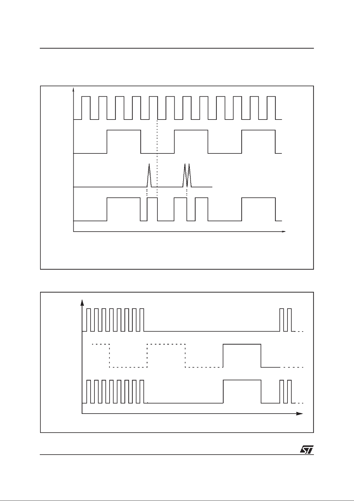
3.1.3 Oscillator Safe Guard
The Oscillator Safe Guard(OSG)affordsdrastically increased operational integrity in ST62xx devices. The OSG circuit provides three basic func-
tions: it filtersspikes from the oscillator lines which
would result in over frequency to the ST62 CPU; it
gives access to the Low Frequency Auxiliary Oscillator (LFAO), used to ensure minimum processing in case of main oscillator failure, to offer reduced power consumption or to provide afixedfrequency low cost oscillator; finally, it automatically
limits the internal clock frequency as a function of
supply voltage, in order to ensure correct operation even if the power supply should drop.
The OSG is enabled or disabled by choosing the
relevant OSG option. It may be viewed as a filter
whose cross-over frequency is device dependent.
Spikes on the oscillator lines result inan effectively
increased internal clock frequency. In the absence
of an OSG circuit, this may lead to an over frequency for a given power supply voltage. The
OSG filters out such spikes(as illustrated in Figure
9). In all cases, when the OSG is active, the maximum internal clock frequency, f
INT
, is limited to
f
OSG
, which is supply voltage dependent. This re-
lationship is illustrated in Figure 12.
When the OSG is enabled, the Low Frequency
Auxiliary Oscillator may be accessed. This oscillator starts operating after the first missing edge of
the main oscillator (see Figure 10).
Over-frequency, at a given power supply level, is
seen by the OSG as spikes; it therefore filters out
some cycles in order that the internal clock frequency of the device is kept within the range the
particular device can stand (depending on VDD),
and below f
OSG
: the maximum authorised frequen-
cy with OSG enabled.
Note. The OSG should be used wherever possible
as it provides maximum safety. Care must be taken, however, as it can increase power consumption and reducethe maximum operating frequency
to f
OSG
.
Warning: Care has to be taken when using the
OSG, as the internal frequency is defined between
a minimum and a maximum value and is not accurate.
For precise timing measurements, it is not recommended to use the OSG and it should notbe enabled in applications that use the SPI or the UART.
It should also be noted that power consumption in
Stop mode is higher when the OSG is enabled
(around 50µA at nominal conditions and room
temperature).
70
ADCR7ADCR6ADCR5ADCR4ADCR3OSC
OFF
ADCR1ADCR
0
15
Page 16
16/70
ST62T00C/T01C ST62T03C/E01C
CLOCK SYSTEM (Cont’d)
Figure 9. OSG Filtering Principle
Figure 10. OSG Emergency Oscillator Principle
(1)
VR001932
(3)
(2)
(4)
(1)
(2)
(3)
(4)
Maximum Frequency for the device to work correctly
Actual Quartz Crystal Frequency at OSCin pin
Noise from OSCin
Resulting Internal Frequency
Main
VR001933
Internal
Emergency
Oscillator
Frequency
Oscillator
16
Page 17
17/70
ST62T00C/T01C ST62T03C/E01C
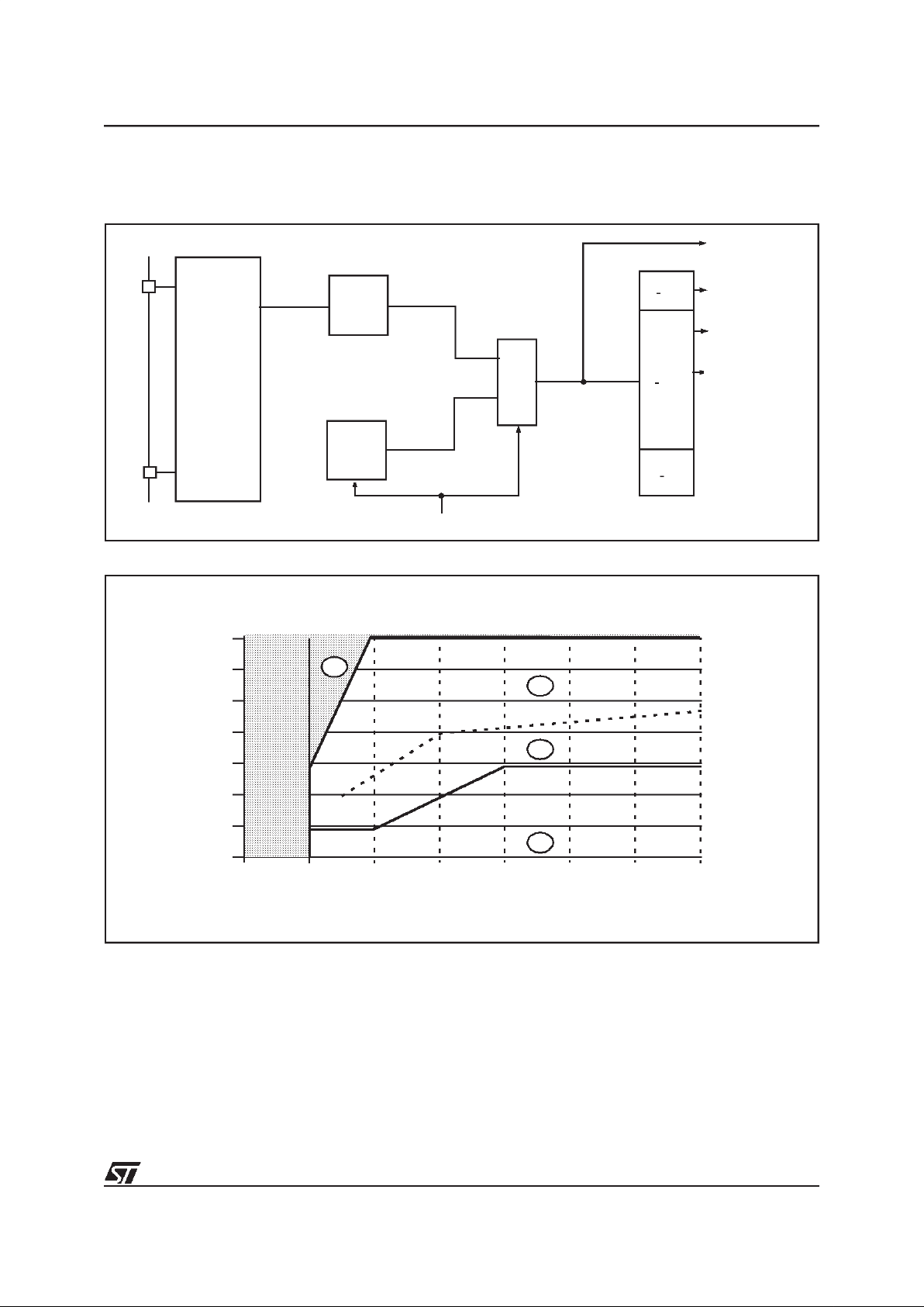
CLOCK SYSTEM (Cont’d)
Figure 11. Clock Circuit Block Diagram
Figure 12. Maximum Operating Frequency (f
MAX
) versus Supply Voltage (VDD)
Notes:
1. In this area, operation is guaranteed at the
quartz crystal frequency.
2. When the OSG is disabled, operation in this
area is guaranteed at the crystal frequency. When
the OSG is enabled, operation in this area is guaranteed at a frequency of at least f
OSG Min.
3. When the OSG is disabled, operation in this
area is guaranteed at the quartz crystalfrequency.
When the OSG is enabled, access to this area is
prevented. The internal frequency is kept a f
OSG.
4. When the OSG is disabled, operation in this
area is not guaranteed
When the OSG is enabled, access to this area is
prevented. The internal frequency is kept at f
OSG.
MAIN
OSCILLATOR
OSG
LFAO
M
U
X
Core
:13
:12
:1
TIMER 1
Watchdog
POR
f
INT
Main Oscillator off
1
2.5 3.6 4 4.5 5 5.5 6
8
7
6
5
4
3
2
Maximum FREQUENCY (MHz)
SUPPLY VOLTAGE (V
DD
)
FUNCTIONALITY IS NOT
3
4
3
2
1
f
OSG
f
OSG
Min
GUARANTEED
IN THIS AREA
VR01807
17
Page 18
18/70
ST62T00C/T01C ST62T03C/E01C
3.2 RESETS
The MCU can be reset in four ways:
– by the external Reset input being pulled low;
– by Power-on Reset;
– by the digital Watchdog peripheral timing out.
– by Low Voltage Detection (LVD)
3.2.1 RESET Input
The RESET pin may be connected to a device of
the application board in order to reset the MCU if
required. The RESET pin may be pulled low in
RUN, WAIT or STOP mode. This input can be
used to reset the MCU internal state and ensure a
correct start-up procedure. The pin is active low
and features a Schmitt trigger input. The internal
Reset signal is generated by adding adelay to the
external signal. Therefore even short pulses on
the RESET pin are acceptable, provided VDDhas
completed its risingphase and that the oscillator is
running correctly (normal RUN or WAIT modes).
The MCU is kept in the Reset state as long as the
RESET pin is held low.
If RESET activation occurs in the RUN or WAIT
modes, processing of the user program is stopped
(RUN modeonly), the Inputs andOutputs are configured as inputs with pull-up resistors and the
main Oscillator is restarted. When the level on the
RESET pin then goes high, the initialization sequence is executed following expiry of the internal
delay period.
If RESET pin activation occurs in the STOP mode,
the oscillator starts up and all Inputs and Outputs
are configured as inputs with pull-up resistors.
When the level of the RESET pin then goes high,
the initialization sequence is executed following
expiry of the internal delay period.
3.2.2 Power-on Reset
The function of the POR circuit consists in waking
up the MCU by detecting around 2V a dynamic
(rising edge) variation of the VDD Supply. At the
beginning of this sequence, the MCU is configured
in the Reset state: all I/O ports are configured as
inputs with pull-up resistors and no instruction is
executed. When the power supply voltage rises to
a sufficient level, the oscillator starts to operate,
whereupon aninternal delay is initiated, in order to
allow the oscillator to fully stabilize before executing the first instruction. The initialization sequence
is executed immediately following the internal delay.
To ensure correct start-up, the user should take
care that the VDD Supply is stabilized at a sufficient level for the chosen frequency (see recommended operation) before the reset signal is released. In addition, supply rising must start from
0V.
As a consequence, the POR doesnot allow to supervise static, slowly rising, or falling, or noisy
(presenting oscillation) VDD supplies.
An external RC network connected to the RESET
pin, or the LVD reset can be used instead to get
the best performances.
Figure 13. Reset and Interrupt Processing
INT LATCH CLEARED
NMI MASK SET
RESET
( IF PRESENT )
SELECT
NMI MODE FLAGS
IS RESETSTILL
PRESENT?
YES
PUT FFEH
ON ADDRESS BUS
FROM RESET LOCATIONS
FFE/FFF
NO
FETCH INSTRUCTION
LOAD PC
VA000427
18
Page 19
19/70
ST62T00C/T01C ST62T03C/E01C
RESETS (Cont’d)
3.2.3 Watchdog Reset
The MCU provides a Watchdog timer function in
order to ensure graceful recovery from software
upsets. If the Watchdog register is not refreshed
before an end-of-count condition is reached, the
internal reset will be activated. This, amongst other things, resets the watchdog counter.
The MCU restarts just as though the Reset had
been generated by the RESET pin, including the
built-in stabilisation delay period.
3.2.4 LVD Reset
The on-chip Low Voltage Detector, selectable as
user option, features static Reset when supply
voltage is below a reference value. Thanks to this
feature, external reset circuit can be removed
while keeping the application safety. This SAFE
RESET is effective as well in Power-on phase as
in power supply drop with different reference val-
ues, allowing hysteresis effect. Reference value in
case of voltage drop has been set lower than the
reference value for power-on in order to avoid any
parasitic Reset when MCU start’s running and
sinking current on the supply.
As long as the supply voltage is below the reference value, there is a internal and static RESET
command. The MCU can start only when the supply voltage rises over the reference value. Therefore, only two operating mode exist for the MCU:
RESET active below the voltage reference, and
running mode over the voltage reference as
shown on the Figure 14, that represents a powerup, power-down sequence.
Note: When the RESET state is controlled by one
of the internal RESET sources (Low Voltage Detector, Watchdog, Power on Reset), the RESET
pin is tied to low logiclevel.
Figure 14. LVD Reset on Power-on and Power-down (Brown-out)
3.2.5 Application Notes
No external resistor is required between VDDand
the Reset pin, thanks to the built-in pull-up device.
Direct external connection of the pin RESET to
VDDmust be avoided in order to ensure safe behaviour of the internal reset sources (AND.Wired
structure).
RESET
RESET
VR02106A
time
V
Up
V
dn
V
DD
19
Page 20
20/70
ST62T00C/T01C ST62T03C/E01C
RESETS (Cont’d)
3.2.6 MCU Initialization Sequence
When a reset occurs the stack is reset, the PC is
loaded with the addressof the Reset Vector (located in programROM starting at address 0FFEh). A
jump tothe beginning of theuser program must be
coded at this address. Following a Reset, the Interrupt flag is automatically set, so that the CPU is
in Non Maskable Interrupt mode; this preventsthe
initialisation routinefrom being interrupted. The initialisation routine should therefore be terminated
by a RETI instruction, in order to revert to normal
mode and enable interrupts. If nopending interrupt
is presentat the endof the initialisation routine, the
MCU will continue by processing the instruction
immediately followingtheRETIinstruction.If,however, a pending interrupt is present, it will be serviced.
Figure 15. Reset and Interrupt Processing
Figure 16. Reset Block Diagram
RESET
RESET
VECTOR
JP
JP:2 BYTES/4 CYCLES
RETI
RETI: 1 BYTE/2CYCLES
INITIALIZATION
ROUTINE
VA00181
V
DD
RESET
R
PU
R
ESD
1)
POWER
WATCHDOG RESET
CK
COUNTER
RESET
ST6
INTERNAL
RESET
f
OSC
RESET
ON RESET
LVD RESET
VR02107A
AND. Wired
1) Resistive ESD protection. Value not guaranteed.
20
Page 21

21/70
ST62T00C/T01C ST62T03C/E01C
RESETS (Cont’d)
Table 4. Register Reset Status
Register Address(es) Status Comment
Oscillator Control Register
Port Data Registers
Port Direction Register
Port Option Register
Interrupt Option Register
TIMER Status/Control
0DCh
0C0h to 0C1h
0C4h to 0C5h
0CCh to 0CDh
0C8h
0D4h
00h
f
INT=fOSC
; OSG disabled
I/O are Input with pull-up
I/O are Input with pull-up
I/O are Input with pull-up
Interrupt disabled
TIMER disabled
X, Y, V, W, Register
Accumulator
Data RAM
Data ROM Window Register
A/D Result Register
080H TO 083H
0FFh
084h to 0BFh
0C9h
0D0h
Undefined As written if programmed
TIMER Counter Register
TIMER Prescaler Register
Watchdog Counter Register
A/D Control Register
0D3h
0D2h
0D8h
0D1h
FFh
7Fh
FEh
40h
Max count loaded
A/D in Standby (When available)
21
Page 22

22/70
ST62T00C/T01C ST62T03C/E01C
3.3 DIGITAL WATCHDOG
The digital Watchdog consists of a reloadable
downcounter timer which can be used to provide
controlled recovery from software upsets.
The Watchdog circuit generates a Resetwhen the
downcounter reaches zero. User software can
prevent this reset by reloading the counter, and
should therefore be written so that the counter is
regularly reloaded while the user program runs
correctly. Inthe event of a software mishap (usually caused by externally generated interference),
the userprogram will no longer behave in its usual
fashion and the timer register will thus not be reloaded periodically. Consequently the timer will
decrement down to 00h and reset the MCU. In order tomaximise the effectiveness of the Watchdog
function, user software must be written with this
concept in mind.
Watchdog behaviour is governed by two options,
known as “WATCHDOG ACTIVATION” (i.e.
HARDWARE or SOFTWARE) and “EXTERNAL
STOP MODE CONTROL”(see Table 5).
In the SOFTWARE option, the Watchdog is disabled until bit C of the DWDR registerhas been set.
When the Watchdog is disabled, low power Stop
mode is available. Once activated, the Watchdog
cannot be disabled, except by resetting the MCU.
In the HARDWARE option, the Watchdog is permanently enabled. Since the oscillator will run continuously, low power mode is not available. The
STOP instruction is interpreted as a WAIT instruction, and the Watchdog continues to countdown.
However, when the EXTERNAL STOP MODE
CONTROL option has been selected low power
consumption may be achieved in Stop Mode.
Execution of the STOP instruction is then governed by a secondary function associated with the
NMI pin. If a STOP instruction is encountered
when the NMI pin is low, it is interpreted as WAIT,
as described above. If, however, the STOP instruction is encountered when the NMI pin is high,
the Watchdog counter is frozen and the CPU enters STOP mode.
When the MCU exits STOP mode(i.e. when aninterrupt is generated), the Watchdog resumes its
activity.
Table 5. Recommended Option Choices
Functions Required Recommended Options
Stop Mode & Watchdog “EXTERNAL STOP MODE” & “HARDWARE WATCHDOG”
Stop Mode “SOFTWARE WATCHDOG”
Watchdog “HARDWARE WATCHDOG”
22
Page 23

23/70
ST62T00C/T01C ST62T03C/E01C
DIGITAL WATCHDOG (Cont’d)
The Watchdog is associated with a Data space
register (Digital WatchDog Register, DWDR, location 0D8h) which is described in greater detail in
Section 3.3.1 Digital Watchdog Register (DWDR).
This register is set to 0FEh on Reset: bit C is
cleared to “0”, which disables the Watchdog; the
timer downcounter bits, T0 to T5, and the SR bit
are allset to“1”, thus selecting the longest Watchdog timer period. This time period can be set tothe
user’s requirements by setting the appropriate value for bits T0 to T5 in the DWDR register. The SR
bit must be set to “1”, since it is this bit which generates the Reset signal when it changes to “0”;
clearing this bit would generate an immediate Reset.
It should be noted that the order of the bits in the
DWDR register is inverted with respect to the associated bits in the down counter: bit 7 of the
DWDR register corresponds, in fact, to T0 and bit
2 to T5. The usershould bear in mind the fact that
these bits are inverted and shifted with respect to
the physicalcounter bits when writing to this register. The relationship between the DWDR register
bits andthe physical implementation oftheWatchdog timer downcounter is illustrated in Figure 17.
Only the6 most significant bits may be usedto define the time period, since it is bit 6 which triggers
the Reset when it changes to “0”. This offers the
user a choice of 64 timed periods ranging from
3,072 to 196,608 clock cycles (with an oscillator
frequency of8MHz, this isequivalent to timer periods ranging from 384µs to 24.576ms).
Figure 17. Watchdog Counter Control
WATCHDOG CONTROL REGISTER
D0
D1
D3
D4
D5
D6
D7
WATCHDOG COUNTER
C
SR
T5
T4
T3
T2
T1
D2
T0
OSC÷12
RESET
VR02068A
÷2
8
23
Page 24

24/70
ST62T00C/T01C ST62T03C/E01C
DIGITAL WATCHDOG (Cont’d)
3.3.1 Digital Watchdog Register (DWDR)
Address: 0D8h — Read/Write
Reset status: 1111 1110b
Bit 0 = C:
Watchdog Control bit
If the hardware option is selected, this bit is forced
high and the user cannotchange it (the Watchdog
is always active). When the software option is selected, the Watchdog function is activated by setting bit C to 1, and cannot then be disabled (save
by resetting the MCU).
When C is kept low the counter can be used as a
7-bit timer.
This bit is cleared to “0” on Reset.
Bit 1 = SR:
Software Reset bit
This bit triggers a Resetwhen cleared.
When C = “0” (Watchdog disabled) it is the MSB of
the 7-bit timer.
This bit is set to “1” on Reset.
Bits 2-7 = T5-T0:
Downcounter bits
It should be noted that the register bits are reversed and shifted with respect to the physical
counter: bit-7 (T0) is the LSB of the Watchdog
downcounter and bit-2 (T5) is the MSB.
These bits are set to “1” on Reset.
3.3.2 Application Notes
The Watchdog plays an important supporting role
in the high noise immunity of ST62xx devices, and
should be used wherever possible. Watchdog related options should be selected on the basis of a
trade-off between application security and STOP
mode availability.
When STOP mode is not required, hardware activation without EXTERNAL STOP MODE CONTROL should be preferred, as it provides maximum security, especially during power-on.
When STOP mode is required, hardware activation and EXTERNAL STOP MODE CONTROL
should be chosen. NMI should be high by default,
to allowSTOP modeto be entered when theMCU
is idle.
The NMI pin can be connected to an I/O line (see
Figure 18) to allow its state to be controlledbysoftware. The I/O line can then be used to keep NMI
low while Watchdog protection is required, or to
avoid noise or key bounce. When no more
processing is required, the I/O line isreleased and
the device placed in STOP modefor lowest power
consumption.
When software activation is selected and the
Watchdog is not activated, the downcounter may
be used as a simple 7-bit timer (remember that the
bits are in reverse order).
The software activation option should be chosen
only when the Watchdog counter is to be used as
a timer. To ensure the Watchdog has not been unexpectedly activated, the following instructions
should be executed within the first 27 instructions:
jrr 0, WD, #+3
ldi WD, 0FDH
70
T0 T1 T2 T3 T4 T5 SR C
24
Page 25

25/70
ST62T00C/T01C ST62T03C/E01C
DIGITAL WATCHDOG (Cont’d)
These instructions test the C bit and Reset the
MCU (i.e. disable the Watchdog) if the bit is set
(i.e. if the Watchdog is active), thus disabling the
Watchdog.
In all modes,a minimum of 28 instructions are executed after activation, before the Watchdog can
generate a Reset. Consequently, user software
should load the watchdog counter within the first
27 instructions following Watchdog activation
(software mode), or within the first 27 instructions
executed following a Reset (hardware activation).
It shouldbe noted that when the GEN bit is low (interrupts disabled), the NMI interrupt is active but
cannot cause a wakeup fromSTOP/WAIT modes.
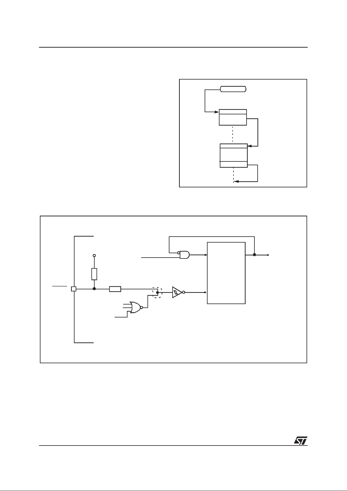
Figure 18. A typical circuit making use of the
EXERNAL STOP MODE CONTROL feature
Figure 19. Digital Watchdog Block Diagram
NMI
SWITCH
I/O
VR02002
RSFF
8
DATA BUS
VA00010
-2
-12
OSCILLATOR
RESET
WRITE
RESET
DB0
R
S
Q
DB1.7 SETLOAD
7
8
-2
SET
CLOCK
25
Page 26

26/70
ST62T00C/T01C ST62T03C/E01C
3.4 INTERRUPTS
The CPU can manage four Maskable Interrupt
sources, in addition to a Non Maskable Interrupt
source (top priorityinterrupt). Each source is associated with a specific Interrupt Vector which contains aJump instruction totheassociated interrupt
service routine. These vectors are located in Program space (see Table 6).
When an interrupt source generates an interrupt
request, and interrupt processing is enabled, the
PC registeris loaded with the address of the interrupt vector (i.e. of the Jump instruction), which
then causes a Jump to the relevant interrupt service routine, thus servicing the interrupt.
Interrupt sourcesare linked to events either onexternal pins, or on chip peripherals. Several events
can be ORed on the same interrupt source, and
relevant flags are available to determine which
event triggered the interrupt.
The Non Maskable Interrupt request has the highest priority and can interrupt any interrupt routine
at any time; the other four interrupts cannot interrupt each other. If more than one interrupt request
is pending, these are processed by the processor
core according to their priority level: source #1 has
the higher priority while source #4 the lower. The
priority of each interrupt source is fixed.
Table 6. Interrupt Vector Map
3.4.1 Interrupt request
All interrupt sources but the Non Maskable Interrupt source can be disabled by setting accordingly
the GEN bit of the Interrupt OptionRegister (IOR).
This GEN bitalso defines if aninterrupt source, including theNonMaskableInterruptsource,can restart the MCU from STOP/WAIT modes.
Interrupt request from the Non Maskable Interrupt
source #0 is latched bya flip flop which isautomat-
ically resetbythe core atthe beginning ofthe nonmaskable interrupt service routine.
Interrupt request from source #1 can be configured either as edgeor level sensitive by setting accordingly theLES bit of the Interrupt Option Register (IOR).
Interrupt request from source #2 are always edge
sensitive. The edge polarity can be configured by
setting accordingly the ESB bit of the Interrupt Option Register (IOR).
Interrupt request from sources #3 & #4 are level
sensitive.
In edgesensitivemode, a latch is set when a edge
occurs on the interrupt source line and is cleared
when the associated interrupt routine is started.
So, the occurrence of an interrupt can be stored,
until completion oftherunning interrupt routine before being processed. If several interrupt requests
occurs before completion of the running interrupt
routine, only the first request is stored.
Storage of interrupt requests is not available inlevel sensitive mode. To be taken into account, the
low level must be present ontheinterruptpinwhen
the MCU samples the line after instruction execution.
At the end of every instruction, the MCU tests the
interrupt lines: if there is an interrupt request the
next instruction is not executed and the appropriate interrupt service routine is executed instead.
Table 7. Interrupt Option Register Description
Interrupt Source Priority Vector Address
Interrupt source #0 1 (FFCh-FFDh)
Interrupt source #1 2 (FF6h-FF7h)
Interrupt source #2 3 (FF4h-FF5h)
Interrupt source #3 4 (FF2h-FF3h)
Interrupt source #4 5 (FF0h-FF1h)
GEN
SET Enable all interrupts
CLEARED Disable all interrupts
ESB
SET
Rising edge mode on interrupt source #2
CLEARED
Falling edge mode on interrupt source #2
LES
SET
Level-sensitive mode on interrupt source #1
CLEARED
Falling edge mode on interrupt source #1
OTHERS NOT USED
26
Page 27

27/70
ST62T00C/T01C ST62T03C/E01C
INTERRUPTS (Cont’d)
3.4.2 Interrupt Procedure
The interrupt procedure is very similartoa call procedure, indeed the user can consider the interrupt
as an asynchronous call procedure. As this is an
asynchronous event, the user cannot know the
context and the time at which it occurred. As a result, the user should save all Data space registers
which may be used within the interrupt routines.
There are separate sets of processor flags for normal, interrupt and non-maskable interrupt modes,
which are automatically switched and so do not
need to be saved.
The following list summarizes the interrupt procedure:
MCU
– The interrupt is detected.
– The C and Z flags are replaced by the interrupt
flags (or by the NMI flags).
– The PC contents are stored in the first level of
the stack.
– The normalinterrupt lines are inhibited (NMI still
active).
– The first internal latch is cleared.
– TheassociatedinterruptvectorisloadedinthePC.
WARNING: In some circumstances, when a
maskable interrupt occurs while the ST6 core is in
NORMAL mode and especially during the execution of an ”ldi IOR, 00h” instruction (disabling all
maskable interrupts):if the interrupt arrives during
the first 3 cycles of the ”ldi” instruction (which is a
4-cycle instruction) the core will switch to interrupt
mode BUT the flags CN and ZN will NOT switch to
the interrupt pair CI and ZI.
User
– User selected registers are saved within the in-
terrupt service routine (normally on a software
stack).
– Thesourceoftheinterruptisfoundbypolling the
interrupt flags (if morethan one source is associ-
ated with the same vector).
– The interrupt is serviced.
– Return from interrupt (RETI)
MCU
– Automatically the MCU switches back to the nor-
mal flag set (or the interrupt flag set) and pops
the previous PC value from the stack.
The interrupt routine usuallybeginsby the identifying the device which generated the interrupt request (bypolling). The user shouldsave the registers which are used within theinterrupt routine in a
software stack. After the RETI instruction is executed, the MCU returns to the main routine.
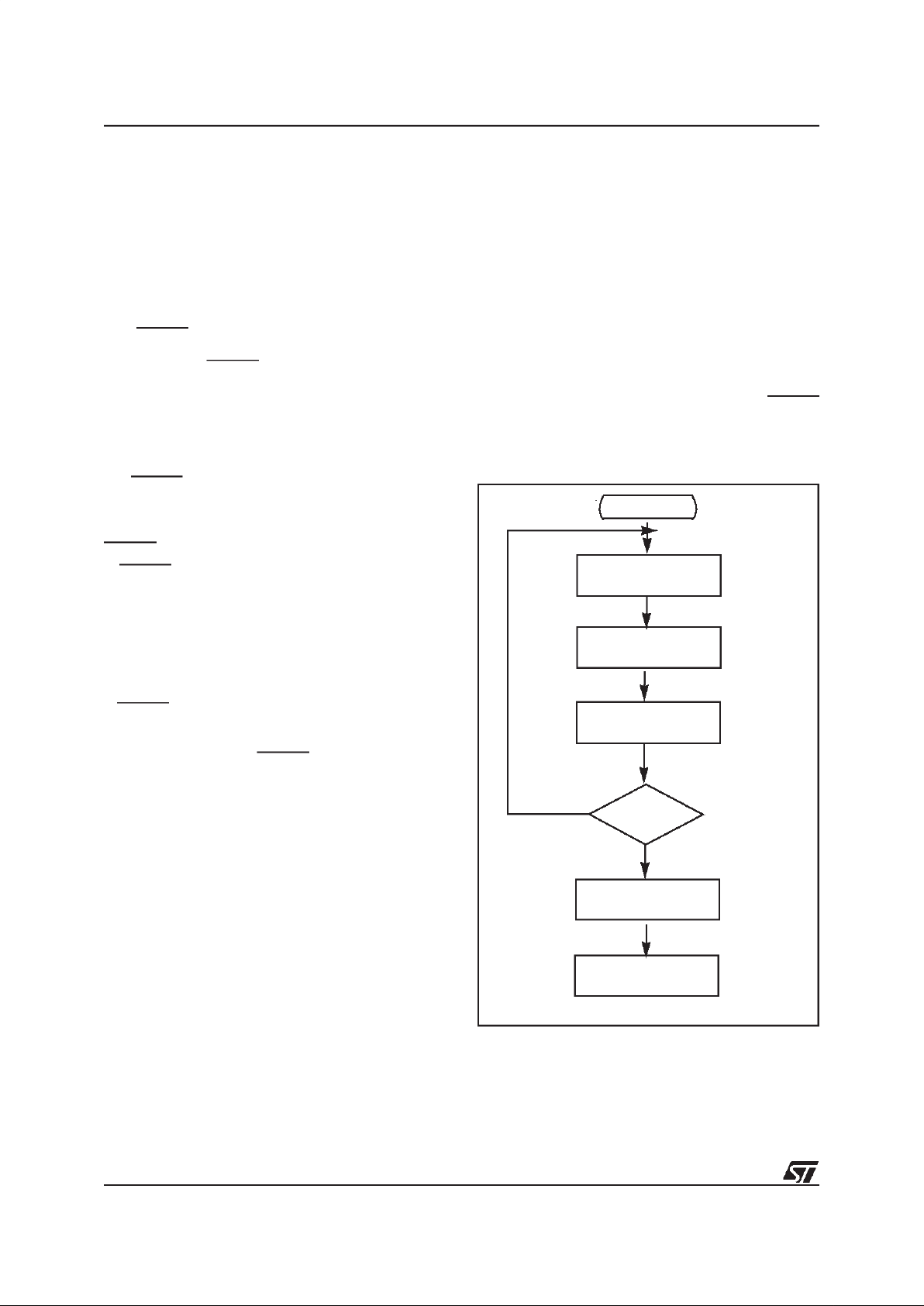
Figure 20. Interrupt Processing Flow Chart
INSTRU CTION
FETCH
INSTRU CTION
EXECUT E
INSTRUCTION
WAS
THE INSTRUCTION
ARETI
?
?
CLEAR
INTERR UPT MASK
SELECT
PROGRAM FLAGS
”POP”
THE STACK ED PC
?
CHEC K IFTHERE IS
AN INTERRUP T R EQUEST
AND INTERRU PT MASK
SELECT
INTER NALMODE FLAG
PUSH THE
PC INTO THE STACK
LOAD PC FROM
INTERR UPT VECTOR
(FFC/FFD)
SET
INTERRUPT MASK
NO
NO
YES
IS THE CORE
ALREADY IN
NORMAL MODE?
VA000014
YES
NO
YES
27
Page 28

28/70
ST62T00C/T01C ST62T03C/E01C
INTERRUPTS (Cont’d)
3.4.3 Interrupt Option Register (IOR)
The Interrupt Option Register (IOR) is used to enable/disable theindividualinterrupt sources and to
select the operating mode of the external interrupt
inputs. This register is write-only and cannot be
accessed by single-bit operations.
Address: 0C8h — Write Only
Reset status: 00h
Bit 7, Bits 3-0 =
Unused
.
Bit 6 = LES:
Level/Edge Selection bit
.
When this bit is set to one, the interrupt source #1
is level sensitive. When cleared to zero the edge
sensitive mode for interrupt request is selected.
Bit 5 = ESB:
Edge Selection bit
.
The bit ESB selects the polarity of the interrupt
source #2.
Bit 4 = GEN:
Global Enable Interrupt
. When this bit
is set to one, all interrupts are enabled. When this
bit is cleared to zero all the interrupts (excluding
NMI) are disabled.
When the GEN bit is low, the NMI interrupt is active butcannot cause a wakeupfrom STOP/WAIT
modes.
This register is cleared on reset.
3.4.4 Interrupt sources
Interrupt sources available on the ST62E01C/
T01C are summarized in the Table 8 with associated mask bit to enable/disable the interrupt request.
Table 8. Interrupt Requests and Mask Bits
*Except ST62T03C
70
- LES ESB GEN - - - -
Peripheral Register
Address
Register
Mask bit Masked Interrupt Source
Interrupt
vector
GENERAL IOR C8h GEN
All Interrupts, excluding
NMI
TIMER TSCR D4h ETI TMZ: TIMER Overflow Vector 3
A/D CONVERTER(*) ADCR D1h EAI EOC: End of Conversion Vector 4
Port PAn ORPA-DRPA C4h-CCh ORPAn-DRPAn PAn pin Vector 1
Port PBn ORPB-DRPB C5h-CDh ORPBn-DRPBn PBn pin Vector 2
28
Page 29

29/70
ST62T00C/T01C ST62T03C/E01C
INTERRUPTS (Cont’d)
Figure 21. Interrupt Block Diagram
NMI
V
DD
FF
CLK Q
CLR
INT #0 - NMI (FFC,D)
I
0
Start
RESTART FROM
STOP/WAI T
INT #1 (FF6,7)
FF
CLK Q
CLR
PBE
0
MUX
1
PORT A
PORT B
Bits
INT #2 (FF4,5)
INT #3 (FF2,3)
TMZ
ETI
TIMER
FF
CLK Q
CLR
IOR REG. C8H, bit 5
I
1
Start
I
2
Start
IOR REG. C8H, bit 6
PBE
PBE
V
DD
FROM REGISTER
SINGLE BIT ENABLE
PORT A,B
PBE
INT #4 (FF0,1)
EAI
EOC
ADC(*)
GEN
VA0426T
(*)Except on ST62T03C
29
Page 30

30/70
ST62T00C/T01C ST62T03C/E01C
3.5 POWER SAVING MODES
The WAIT and STOP modes have been implemented in the ST62xx family of MCUs in order to
reduce theproduct’selectricalconsumption during
idle periods. These two power saving modes are
described in the following paragraphs.
In addition, the Low Frequency Auxiliary Oscillator
(LFAO) can be used instead of the main oscillator
to reduce power consumption in RUN and WAIT
modes.
3.5.1 WAIT Mode
The MCU goes into WAIT mode as soon as the
WAIT instruction is executed. The microcontroller
can be considered as being in a “software frozen”
state where the core stops processing the program instructions, the RAMcontentsand peripheral registers are preserved as long as the power
supply voltage is higher than the RAM retention
voltage. In this mode the peripherals are still active.
WAIT mode can be used when the user wants to
reduce the MCU power consumption during idle
periods, while not losing track of timeor the capability of monitoring external events. The active oscillator (main oscillator or LFAO) is not stopped in
order to provide a clock signal to the peripherals.
Timer counting may be enabled as well as the
Timer interrupt, before entering the WAIT mode:
this allows the WAIT mode to be exited when a
Timer interrupt occurs. The same applies to other
peripherals which usethe clock signal.
If the power consumption has to be further reduced, the Low Frequency Auxiliary Oscillator
(LFAO) canbeusedin place ofthe main oscillator,
if its operating frequency is lower. If required, the
LFAO must be switched on before entering the
WAIT mode.
If the WAIT mode is exited due to a Reset (either
by activating the external pin or generated by the
Watchdog), the MCU enters a normal reset procedure. If an interrupt is generated during WAIT
mode, the MCU’s behaviour depends on the state
of theprocessor coreprior to the WAIT instruction,
but also on the kind of interrupt request which is
generated. This is described in the following paragraphs. The processor core does not generate a
delay following the occurrence of the interrupt, because the oscillator clock is still available and no
stabilisation period is necessary.
3.5.2 STOP Mode
If the Watchdog is disabled, STOP mode is available. When in STOP mode, the MCU is placed in
the lowest power consumption mode. In this operating mode, the microcontrollercan be considered
as being “frozen”, no instruction is executed, the
oscillator is stopped, the RAM contents and peripheral registers are preserved as long as the
power supply voltage is higher than the RAM retention voltage, and the ST62xx core waits for the
occurrence of an external interrupt request or a
Reset to exit the STOP state.
If the STOP state is exited due to a Reset (by activating the external pin) the MCU will enter a normal reset procedure. Behaviour in response to interrupts depends on the state of the processor
core prior to issuing the STOP instruction, and
also on the kind of interrupt request that is generated.
This case will be described in the following paragraphs. The processor core generates a delay after occurrence of the interrupt request, in order to
wait for complete stabilisation of the oscillator, before executing the first instruction.
30
Page 31

31/70
ST62T00C/T01C ST62T03C/E01C
POWER SAVING MODE (Cont’d)
3.5.3 Exit from WAIT and STOP Modes
The following paragraphs describe how the MCU
exits fromWAIT and STOP modes, when an interrupt occurs (not a Reset). It should be noted that
the restart sequence depends on the original state
of the MCU (normal, interrupt or non-maskable interrupt mode) prior to entering WAIT or STOP
mode, as well as on the interrupt type.
Interrupts do not affect the oscillator selection,
consequently, when the LFAO is used, the user
program mustmanage oscillator selection as soon
as normal RUN mode is resumed.
3.5.3.1 Normal Mode
If the MCUwasin themain routine when the WAIT
or STOP instruction was executed, exit from Stop
or Waitmodewill occur as soon as an interrupt occurs; the related interrupt routine is executed and,
on completion, the instruction which follows the
STOP or WAIT instruction is then executed, providing no other interrupts are pending.
3.5.3.2 Non Maskable Interrupt Mode
If the STOP or WAIT instruction has been executed during execution of the non-maskable interrupt
routine, theMCU exits from the Stop or Wait mode
as soon as an interrupt occurs: the instruction
which follows the STOP or WAIT instruction is executed, and the MCU remains innon-maskable interrupt mode, even if another interrupt has been
generated.
3.5.3.3 Normal Interrupt Mode
If theMCU was in interrupt mode before the STOP
or WAIT instruction was executed, it exits from
STOP or WAIT mode as soon as an interrupt occurs. Nevertheless, two cases must be considered:
– If the interrupt is a normal one, the interrupt rou-
tine in which the WAIT or STOP mode was en-
tered will be completed, starting with the
execution of the instruction which follows the
STOP or the WAIT instruction, and the MCU is
still in the interrupt mode. At the end of this routine pending interrupts will be serviced in accordance with their priority.
– In the event of a non-maskable interrupt, the
non-maskable interrupt service routine is processed first,thentheroutine in which the WAIT or
STOP mode was entered will be completed by
executing the instruction following the STOP or
WAIT instruction. The MCU remains in normal interrupt mode.
Notes:
To achieve the lowest power consumption during
RUN or WAIT modes, the user program must take
care of:
– configuring unused I/Osasinputswithoutpull-up
(these should beexternally tied to well defined
logic levels);
– placing all peripherals in their power down
modes before entering STOP mode;
– selectingtheLow Frequency Auxiliary Oscillator
(provided thisruns at a lowerfrequency than the
main oscillator).
When the hardware activated Watchdog is selected, or when the software Watchdogisenabled,the
STOP instruction is disabled and a WAIT instruction will be executed in its place.
If all interrupt sources are disabled (GEN low), the
MCU can only be restarted by a Reset. Although
setting GEN low does not mask the NMI as an interrupt, it will stop it generating a wake-upsignal.
The WAIT and STOP instructions are not executed if an enabled interrupt request is pending.
31
Page 32

32/70
ST62T00C/T01C ST62T03C/E01C
4 ON-CHIP PERIPHERALS
4.1 I/O PORTS
The MCU features Input/Output lines which may
be individuallyprogrammedas any of the following
input or output configurations:
– Input withoutpull-up or interrupt
– Input with pull-up and interrupt
– Input with pull-up, but without interrupt
– Analog input
– Push-pull output
– Open drain output
The lines are organised as bytewise Ports.
Each port is associated with 3 registers in Data
space. Each bit of these registers is associated
with a particular line (for instance, bits 0 of Port A
Data, Direction and Option registers are associated with the PA0 line of Port A).
The DATA registers (DRx), are used to read the
voltage level values of the lines which have been
configured as inputs, or to write the logic value of
the signal to be output on the lines configured as
outputs. Theport data registers can be read to get
the effective logic levels of the pins, but they can
be also written by user software, in conjunction
with the related option registers, to select the different input mode options.
Single-bit operations on I/O registers are possible
but care is necessary because reading in input
mode is done fromI/O pins while writing will directly affect the Port data register causing an undesired change of the input configuration.
The Data Direction registers (DDRx) allow the
data direction (input or output) of each pin to be
set.
The Option registers (ORx) are used to select the
different port options available both in input and in
output mode.
All I/O registers can be read or written to just as
any other RAM location inData space, so no extra
RAM cells are needed for port data storage and
manipulation. During MCU initialization, all I/Oregisters are cleared andthe input mode with pull-ups
and no interrupt generation is selected for all the
pins, thus avoiding pin conflicts.
Figure 22. I/O PortBlock Diagram
V
DD
RESET
S
IN
CONTROLS
S
OUT
SHIFT
REGISTER
DATA
DATA
DIRECTION
REGISTER
REGISTER
OPTION
REGISTER
INPUT/OUTPUT
TO INTERRUPT
V
DD
TO ADC
VA00413
32
Page 33

33/70
ST62T00C/T01C ST62T03C/E01C
I/O PORTS (Cont’d)
4.1.1 Operating Modes
Each pinmay be individually programmed asinput
or output with various configurations.
This is achieved by writing the relevant bit in the
Data (DR), Data Direction (DDR) and Option registers (OR). Table 9 illustrates the various port
configurations which can be selected by user software.
4.1.1.1 Input Options
Pull-up, High Impedance Option. All input lines
can be individually programmed with or without an
internal pull-up by programming the OR and DR
registers accordingly. If the pull-up option is not
selected, the input pin will be in the high-impedance state.
4.1.1.2 Interrupt Options
All input lines can be individually connected by
software to the interrupt system by programming
the OR and DR registers accordingly. The interrupt trigger modes (falling edge, rising edge and
low level) can be configured by software as described in the Interrupt Chapter for each port.
4.1.1.3 Analog Input Options
Some pins can be configured as analog inputs by
programming the OR and DR registers accordingly. These analog inputs are connected to the onchip 8-bit Analog to Digital Converter.
ONLY ONE
pin should be programmed as an analog input at
any time, since by selecting more than one input
simultaneously their pins will be effectively shorted.
Table 9. I/O Port Option Selection
Note: X = Don’t care
DDR OR DR Mode Option
0 0 0 Input With pull-up, no interrupt
0 0 1 Input No pull-up, no interrupt
0 1 0 Input With pull-up and with interrupt
0 1 1 Input Analog input (when available)
1 0 X Output Open-drain output (20mA sink when available)
1 1 X Output Push-pull output (20mA sink when available)
33
Page 34

34/70
ST62T00C/T01C ST62T03C/E01C
I/O PORTS (Cont’d)
4.1.2 Safe I/O State Switching Sequence
Switching the I/O ports from one state to another
should be done in a sequence which ensures that
no unwanted side effects can occur. The recommended safe transitions are illustrated in Figure
23. All other transitions are potentially risky and
should be avoided when changing the I/O operating mode,as itis most likely that undesirable sideeffects willbeexperienced, such asspuriousinterrupt generation ortwo pins shorted together by the
analog multiplexer.
Single bit instructions (SET, RES, INC and DEC)
should be used with great caution on Ports Data
registers, since these instructions make an implicit
read and write back of the entire register. In port
input mode, however, the data register reads from
the input pins directly, and not from the data register latches. Since data registerinformation in input
mode is used to set the characteristics of the input
pin (interrupt, pull-up, analog input), these may be
unintentionally reprogrammed depending on the
state ofthe input pins. As ageneral rule, itisbetter
to limit the use of single bit instructions on data
registers to when the whole (8-bit) port is in output
mode. In the case of inputs or of mixed inputs and
outputs, it is advisable to keep a copy of the data
register in RAM. Single bit instructions may then
be used on the RAM copy, after which the whole
copy register can be written to the port data register:
SET bit, datacopy
LD a, datacopy
LD DRA, a
Warning: Care must also be taken to not use instructions that act on a whole port register (INC,
DEC, or read operations) when all 8 bits are not
available on the device. Unavailable bits must be
masked by software (AND instruction).
The WAIT and STOP instructions allow the
ST62xx to be used in situations where low power
consumption is needed. The lowest power consumption is achieved by configuring I/Os in input
mode with well-defined logic levels.
The usermust take care not to switch outputs with
heavy loads during the conversion of one of the
analog inputs in order to avoid any disturbance to
the conversion.
Figure 23. Diagram showingSafe I/O State Transitions
Note *. xxx = DDR, OR, DR Bits respectively
Interrupt
pull-up
Output
Open Drain
Output
Push-pull
Input
pull-up (Reset
state)
Input
Analog
Output
Open Drain
Output
Push-pull
Input
010*
000
100
110
011
001
101
111
34
Page 35

35/70
ST62T00C/T01C ST62T03C/E01C
I/O PORTS (Cont’d)
4.1.3 I/O Port Option Registers
ORA/B (CCh PA, CDh PB) Read/Write
Bit 7-0 = Px7 - Px0:
Port A and B Option Register
bits.
4.1.4 I/O Port Data Direction Registers
DDRA/B (C4h PA, C5h PB) Read/Write
Bit 7-0 = Px7 - Px0:
Port A and B Data Direction
Registers bits.
4.1.5 I/O Port Data Registers
DRA/B (C0h PA, C1h PB) Read/Write
Bit 7-0 = Px7 - Px0:
Port A and B Data Registers
bits.
Note: X = Don’t care
70
Px7 Px6 Px5 Px4 Px3 Px2 Px1 Px0
70
Px7 Px6 Px5 Px4 Px3 Px2 Px1 Px0
70
Px7 Px6 Px5 Px4 Px3 Px2 Px1 Px0
35
Page 36

36/70
ST62T00C/T01C ST62T03C/E01C
I/O PORTS (Cont’d)
Table 10. I/O Port Option Selections
Note 1. Provided the correct configuration has been selected.
MODE AVAILABLE ON
(1)
SCHEMATIC
Input
PA1-PA3
PB0,PB1,PB3,PB5-PB7
Input
with pull up
PA1-PA3
PB0,PB1,PB3,PB5-PB7
Input
with pull up
with interrupt
PA1-PA3
PB0,PB1,PB3,PB5-PB7
Analog Input
PB3,PB5-PB7
(Except ST62T03C)
Open drain output
5mA
Open drain output
20mA
PB0,PB1,PB3,PB5-PB7
PA1-PA3
Push-pull output
5mA
Push-pull output
20mA
PB0,PB1,PB3,PB5-PB7
PA1-PA3
Data in
Interrupt
Data in
Interrupt
Data in
Interrupt
Data out
ADC
Data out
36
Page 37

37/70
ST62T00C/T01C ST62T03C/E01C
4.2 TIMER
The MCU features an on-chip Timer peripheral,
consisting ofan 8-bit counter with a 7-bit programmable prescaler, giving a maximum count of 215.
Figure 24 shows the Timer Block Diagram. The
content of the 8-bit counter can be read/written in
the Timer/Counterregister,TCR, which can be addressed in Data space as a RAM location at address 0D3h. The state of the 7-bit prescaler canbe
read in the PSC register at address 0D2h. The
control logic device is managed in the TSCR register as described in thefollowing paragraphs.
The 8-bit counter is decrement by the output (rising edge) coming from the 7-bit prescaler and can
be loaded and read under program control. When
it decrements tozero then the TMZ (Timer Zero)bit
in the TSCR is set. If the ETI (Enable Timer Interrupt) bit in the TSCR is also set, an interrupt request is generated. The Timer interrupt can be
used to exit the MCU from WAIT mode.
The prescaler input is the internal frequency (f
INT
)
divided by 12. The prescaler decrements on the
rising edge. Depending on the division factor programmed by PS2, PS1 and PS0 bits in the TSCR
(see Figure 11), the clock input of the timer/counter register is multiplexed to different sources. For
division factor 1, the clock input of the prescaler is
also that of timer/counter; for factor 2, bit 0 of the
prescaler register is connected to the clock input of
TCR. This bit changes itsstate at half the frequency ofthe prescalerinput clock. For factor 4, bit 1of
the PSC is connected to the clock input of TCR,
and so forth. The prescaler initialize bit, PSI, in the
TSCR register must be set to allow the prescaler
(and hence the counter) to start. If it is cleared, all
the prescaler bits are set and the counter is inhibited from counting. The prescaler can be loaded
with any value between 0and 7Fh, if bit PSI is set.
The prescaler tap is selected by means of the
PS2/PS1/PS0 bits in the control register.
Figure 25 illustrates the Timer’s working principle.
Figure 24. Timer Block Diagram
DATA BUS
8-BIT
COUNTER
STATUS/CONTROL
REGISTER
INTERRUPT
LINE
VR02070A
3
8
8
8
6
5
4
3
2
1
0
SELECT
1OF7
12
b7 b6 b5 b4 b3 b2 b1 b0
TMZ ETI D5 D4 PSI PS2 PS1 PS0
f
INT
PSC
37
Page 38

38/70
ST62T00C/T01C ST62T03C/E01C
TIMER (Cont’d)
4.2.1 Timer Operation
The Timer prescaler is clocked by the prescaler
clock input (f
INT
÷ 12).
The user can select the desired prescaler division
ratio through the PS2, PS1, PS0 bits. When the
TCR count reaches 0, it sets the TMZ bit in the
TSCR. The TMZ bit can be tested under program
control to perform a timer function whenever it
goes high.
4.2.2 Timer Interrupt
When the counterregister decrements to zero with
the ETI (Enable Timer Interrupt) bit set to one, an
interrupt request associated with Interrupt Vector
#3 is generated. When the counter decrements to
zero, the TMZ bit in the TSCR register is set to
one.
4.2.3 Application Notes
TMZ is set when the counter reaches zero; however, it may also be set by writing 00h in the TCR
register or by setting bit 7 of the TSCR register.
The TMZ bit must be cleared by user software
when servicing the timer interrupt to avoid undesired interrupts when leaving the interrupt service
routine. After reset, the 8-bit counter register is
loaded with 0FFh, while the7-bit prescaler is loaded with 07Fh, and the TSCR register is cleared.
This means that the Timer is stopped (PSI=“0”)
and the timer interrupt is disabled.
Figure 25. Timer Working Principle
BIT0 BIT1 BIT2 BIT3 BIT6BIT5BIT4
CLOCK
7-BIT PRESCALER
8-1 MULTIPLEXER
8-BIT COUNTER
BIT0 BIT1
BIT2
BIT3 BIT4 BIT5
BIT6
BIT7
10234
5
67
PS0
PS1
PS2
VA00186
38
Page 39

39/70
ST62T00C/T01C ST62T03C/E01C
TIMER (Cont’d)
A write to the TCR register will predominate over
the 8-bit counter decrement to00h function, i.e.if a
write and a TCR register decrement to 00h occur
simultaneously, the write will take precedence,
and the TMZ bit is not set until the 8-bit counter
reaches 00hagain. The valuesof the TCR and the
PSC registers can be read accurately at anytime.
4.2.4 Timer Registers
Timer Status Control Register (TSCR)
Address: 0D4h — Read/Write
Bit 7 = TMZ:
Timer Zero bit
A low-to-high transition indicates that the timer
count register has decrement to zero. This bit
must becleared by user software before starting a
new count.
Bit 6 = ETI:
Enable Timer Interrup
When set, enables the timer interrupt request
(vector #3).If ETI=0 the timer interrupt is disabled.
If ETI=1 and TMZ=1 an interrupt request is generated.
Bit 5 = D5:
Reserved
Must be set to “1”.
Bit 4 = D4
Do not care.
Bit 3 = PSI:
Prescaler Initialize Bit
Used toinitialize theprescalerand inhibit its counting. When PSI=“0” the prescaler is set to 7Fh and
the counteris inhibited.When PSI=“1”theprescaler is enabled to count downwards. As long as
PSI=“0” both counter and prescaler are not running.
Bit 2, 1, 0 = PS2, PS1, PS0:
Prescaler Mux. Se-
lect.
These bitsselect the division ratio of thepres-
caler register.
Table 11. Prescaler Division Factors
Timer Counter Register TCR
Address: 0D3h — Read/Write
Bit 7-0 = D7-D0:
Counter Bits.
Prescaler Register PSC
Address: 0D2h — Read/Write
Bit 7 = D7: Always read as ”0”.
Bit 6-0 = D6-D0: Prescaler Bits.
70
TMZ ETI D5 D4 PSI PS2 PS1 PS0
PS2 PS1 PS0 Divided by
0001
0012
0104
0118
10016
10132
11064
1 1 1 128
70
D7 D6 D5 D4 D3 D2 D1 D0
70
D7 D6 D5 D4 D3 D2 D1 D0
39
Page 40

40/70
ST62T00C/T01C ST62T03C/E01C
4.3 A/D CONVERTER (ADC)
The A/D converter peripheral is an 8-bit analog to
digital converter with analog inputs asalternateI/O
functions (the number of which is device dependent), offering 8-bit resolution with a typical conversion time of 70us (at an oscillator clock frequency
of 8MHz).
The ADC converts the input voltage by a process
of successive approximations, using a clock frequency derived from the oscillator with a division
factor of twelve. With an oscillator clock frequency
less than 1.2MHz, conversion accuracy is decreased.
Selection of the input pin is done by configuring
the related I/O line as an analog input via the Option and Data registers (refer to I/O ports description for additional information). Only one I/O line
must beconfigured as an analog input at any time.
The user must avoid any situation in which more
than one I/O pin is selected as an analog input simultaneously, to avoid device malfunction.
The ADCuses two registers in the data space: the
ADC data conversion register, ADR, which stores
the conversion result, and the ADC control register, ADCR, used to program the ADC functions.
A conversion is started by writing a “1” to the Start
bit (STA) in the ADC control register. This automatically clears (resets to “0”) the End Of Conversion Bit (EOC). When a conversion is complete,
the EOC bit is automatically set to “1”, in order to
flag that conversion is complete and that the data
in the ADC data conversion register is valid. Each
conversion has to be separately initiated bywriting
to the STA bit.
The STA bit is continuously scanned so that, if the
user sets it to “1” whilea previous conversion is in
progress, a new conversion is started before completing the previous one. The start bit (STA) is a
write onlybit,anyattempt to read itwill show a logical “0”.
The A/D converter features a maskable interrupt
associated with the end of conversion. This interrupt is associated with interrupt vector #4 and occurs when the EOC bit is set (i.e. when a conversion is completed). The interrupt is masked using
the EAI (interrupt mask) bit in the control register.
The power consumption of the device can be reduced by turning off the ADC peripheral. This is
done bysettingthe PDS bitin the ADC controlregister to “0”. If PDS=“1”, the A/D is powered andenabled for conversion. This bit must be set at least
one instruction beforethe beginningof the conver-
sion to allow stabilisation of the A/D converter.
This action is also needed before entering WAIT
mode, since the A/D comparator is not automatically disabled in WAIT mode.
During Reset, any conversion in progress is
stopped, the control register is reset to 40h andthe
ADC interrupt is masked (EAI=0).
Figure 26. ADC Block Diagram
4.3.1 Application Notes
The A/D converter does not feature a sample and
hold circuit. The analog voltage to be measured
should therefore be stable during the entire conversion cycle. Voltage variation should not exceed
±1/2 LSB for the optimum conversion accuracy. A
low pass filter may be used at the analog input
pins to reduce input voltage variation during conversion.
When selected asan analog channel, the input pin
is internally connected to a capacitor Cadof typically 12pF. For maximum accuracy, this capacitor
must be fully charged at the beginning of conversion. In the worst case, conversion starts one instruction (6.5 µs) after the channel has been selected. In worst case conditions, the impedance,
ASI, of the analog voltage sourceis calculated using the following formula:
6.5µs=9xCadx ASI
(capacitor charged to over 99.9%), i.e. 30 kΩ including a 50% guardband. ASI can behigher if C
ad
has been charged for a longer period by adding instructions before the start of conversion (adding
more than 26 CPU cycles is pointless).
CONTROL REGISTER
CONVERTER
VA00418
RESULT REGISTER
RESET
INTERRUPT
CLOCK
AV
AV
DD
Ain
8
CORE
CONTROL SIGNALS
SS
8
CORE
40
Page 41

41/70
ST62T00C/T01C ST62T03C/E01C
A/D CONVERTER (Cont’d)
Since the ADC is on the same chip as the microprocessor, theusershouldnotswitch heavily loaded output signals during conversion, if high precision is required.Such switchingwill affectthe supply voltages used as analog references.
The accuracy of the conversion depends on the
quality of the power supplies (VDDand VSS). The
user must take special care to ensure a well regulated reference voltage is present on the VDDand
VSSpins (power supplyvoltage variations must be
less than 5V/ms). This implies, in particular, that a
suitable decoupling capacitor is used at the V
DD
pin.
The converter resolution is given by::
The Input voltage (Ain) which is to be converted
must be constant for 1µs before conversion and
remain constant during conversion.
Conversion resolution can be improved if the power supply voltage (VDD) to the microcontroller is
lowered.
In orderto optimise conversion resolution,the user
can configure the microcontroller in WAIT mode,
because this mode minimises noise disturbances
and power supply variations due to output switching. Nevertheless, the WAIT instruction should be
executed as soon as possible after the beginning
of the conversion, because execution of the WAIT
instruction may cause a small variation of the V
DD
voltage. The negativeeffectofthisvariationisminimized at the beginning oftheconversion when the
converter is less sensitive, rather than at the end
of conversion, when the less significant bits are
determined.
The best configuration, from an accuracy standpoint, is WAIT mode with the Timer stopped. Indeed, only the ADC peripheral and the oscillator
are then still working. TheMCU must be woken up
from WAIT mode by the ADC interrupt at the end
of the conversion. It should be noted that waking
up the microcontroller could also be done using
the Timer interrupt, but in this case the Timer will
be working and the resulting noise could affect
conversion accuracy.
A/D Converter Control Register (ADCR)
Address: 0D1h — Read/Write
Bit 7 =EAI:
Enable A/D Interrupt.
If this bit is set to
“1” the A/D interrupt is enabled, when EAI=0 the
interrupt is disabled.
Bit 6 = EOC:
End of conversion. Read Only
. This
read only bit indicates when a conversion has
been completed. This bit is automatically reset to
“0” when the STA bit is written. If the user is using
the interrupt option then this bit can be used as an
interrupt pending bit. Data in the data conversion
register are valid only when this bit is set to “1”.
Bit 5 = STA
: Start of Conversion. Write Only
. Writing a“1” to this bitwillstart a conversion on the selected channel and automatically reset to “0” the
EOC bit. If the bit is set again when aconversion is
in progress, the present conversion isstopped and
a new one will takeplace. This bit iswrite only, any
attempt to read it will show a logical zero.
Bit 4 = PDS
: Power Down Selection.
This bit activates the A/D converter if setto “1”. Writing a“0” to
this bit will put the ADC in power down mode (idle
mode).
Bit 3-0 = D3-D0. Not used
A/D Converter Data Register (ADR)
Address: 0D0h — Read only
Bit 7-0 = D7-D0
: 8 Bit A/D Conversion Result.
V
DDVSS
–
256
----------------------------
70
EAI EOC STA PDS D3 D2 D1 D0
70
D7 D6 D5 D4 D3 D2 D1 D0
41
Page 42

42/70
ST62T00C/T01C ST62T03C/E01C
5 SOFTWARE
5.1 ST6 ARCHITECTURE
The ST6 software has been designed to fully use
the hardware in the most efficient way possible
while keeping byte usage to a minimum; in short,
to provide byte efficient programming capability.
The ST6 core has the ability to set or clear any
register or RAM location bit ofthe Data space with
a single instruction. Furthermore, the program
may branch to a selected address depending on
the status of any bit of the Data space. The carry
bit is stored with thevalue of the bit when the SET
or RES instruction is processed.
5.2 ADDRESSING MODES
The ST6 core offers nine addressing modes,
which are described in the following paragraphs.
Three different address spaces are available: Program space, Data space, and Stack space. Program space contains the instructions which are to
be executed, plus the data for immediate mode instructions. Data space contains the Accumulator,
the X,Y,V and W registers, peripheral and Input/
Output registers, the RAM locations and Data
ROM locations (for storage of tables and constants). Stack space contains six 12-bit RAM cells
used tostack the return addresses forsubroutines
and interrupts.
Immediate. In the immediate addressing mode,
the operand of the instruction follows the opcode
location. Asthe operand is aROM byte, the immediate addressing mode is used to access constants whichdonot changeduringprogram execution (e.g.,a constant used toinitialize a loop counter).
Direct. In the direct addressing mode, the address
of the byte whichis processed by the instruction is
stored inthe locationwhichfollows the opcode. Direct addressing allows the user to directly address
the 256 bytes in Data Space memory with a single
two-byte instruction.
Short Direct. The core canaddress the four RAM
registers X,Y,V,W (locations 80h, 81h,82h,83h) in
the short-direct addressing mode. In thiscase, the
instruction is only one byte and the selection ofthe
location to be processed is contained in the opcode. Short direct addressing is a subset of the direct addressing mode. (Note that 80h and 81h are
also indirect registers).
Extended. In the extended addressing mode, the
12-bit address needed to define the instruction is
obtained by concatenating the four less significant
bits of the opcode with the byte following the opcode. The instructions (JP, CALL) which use the
extended addressing mode are able to branch to
any address of the 4K bytes Program space.
An extended addressing mode instruction is twobyte long.
Program Counter Relative. Therelativeaddressing mode is only used in conditional branch instructions. The instruction isused to perform atest
and, if the condition is true, a branch with aspan of
-15 to +16 locations around the address of the relative instruction. If the condition is not true, the instruction which follows the relative instruction is
executed. The relative addressing mode instruction is one-byte long. The opcode is obtained in
adding the three most significant bits which characterize the kind of the test, one bit which determines whether the branch is a forward (when it is
0) or backward (when it is 1) branch and the four
less significant bits which give the span of the
branch (0h to Fh) which must be added or subtracted to the address of the relative instruction to
obtain the address of thebranch.
Bit Direct. In the bit direct addressing mode, the
bit to be set or cleared is part of the opcode, and
the byte following the opcode points to the address of the byte in which the specified bit mustbe
set orcleared. Thus, any bitin the256 locations of
Data space memory can be set or cleared.
Bit Test & Branch. The bit test and branch addressing mode is a combination of direct addressing and relative addressing. The bit test and
branch instruction is three-byte long. The bit identification and the tested condition are included in
the opcode byte. The address of the byte to be
tested follows immediately the opcode in the Program space. The third byte is the jump displacement, which is in the range of -127 to +128. This
displacement can be determined using a label,
which is converted by the assembler.
Indirect. Inthe indirect addressingmode, the byte
processed by the register-indirect instruction is at
the address pointed by the content of one of the indirect registers, X or Y (80h,81h). The indirect register is selected by thebit4 of the opcode. A register indirect instruction is one byte long.
Inherent. In the inherent addressing mode, all the
information necessary to execute the instruction is
contained in the opcode. These instructions are
one byte long.
42
Page 43

43/70
ST62T00C/T01C ST62T03C/E01C
5.3 INSTRUCTION SET
The ST6 core offers a set of 40 basic instructions
which, when combined with nine addressing
modes, yield244 usable opcodes.They can be divided into six different types: load/store, arithmetic/logic, conditional branch, control instructions,
jump/call, and bit manipulation. The following paragraphs describe the different types.
All the instructions belonging to a given type are
presented in individual tables.
Load & Store. These instructions use one, two or
three bytes in relation with the addressing mode.
One operand is the Accumulator for LOAD andthe
other operand is obtained fromdata memory using
one of the addressing modes.
For Load Immediate one operand can be any of
the 256 data space bytes while theother is always
immediate data.
Table 12. Load & Store Instructions
Notes:
X,Y. Indirect Register Pointers, V & W Short Direct Registers
# . Immediate data (stored in ROM memory)
rr. Data space register
∆. Affected
* . Not Affected
Instruction Addressing Mode Bytes Cycles
Flags
ZC
LD A, X Short Direct 1 4 ∆ *
LD A, Y Short Direct 1 4 ∆ *
LD A, V Short Direct 1 4 ∆ *
LD A, W Short Direct 1 4 ∆ *
LD X, A Short Direct 1 4 ∆ *
LD Y, A Short Direct 1 4 ∆ *
LD V, A Short Direct 1 4 ∆ *
LD W,A Short Direct 1 4 ∆ *
LD A, rr Direct 2 4 ∆ *
LD rr,A Direct 2 4 ∆ *
LD A, (X) Indirect 1 4 ∆ *
LD A, (Y) Indirect 1 4 ∆ *
LD (X), A Indirect 1 4 ∆ *
LD (Y), A Indirect 1 4 ∆ *
LDI A, #N Immediate 2 4 ∆ *
LDI rr,#N Immediate 3 4 * *
43
Page 44

44/70
ST62T00C/T01C ST62T03C/E01C
INSTRUCTION SET (Cont’d)
Arithmetic and Logic. These instructions are
used to perform the arithmetic calculations and
logic operations. In AND, ADD, CP, SUB instructions oneoperandis alwaystheaccumulator while
the other can be either a data space memory con-
tent or an immediate value in relation with the addressing mode. In CLR, DEC, INC instructions the
operand can be any of the 256 data space addresses. In COM, RLC, SLA the operand is always
the accumulator.
Table 13. Arithmetic & Logic Instructions
Notes:
X,Y.Indirect Register Pointers, V & W Short Direct RegistersD. Affected
# . Immediate data (stored in ROM memory)* . Not Affected
rr. Data space register
Instruction Addressing Mode Bytes Cycles
Flags
ZC
ADD A, (X) Indirect 1 4 ∆∆
ADD A, (Y) Indirect 1 4 ∆∆
ADD A, rr Direct 2 4 ∆∆
ADDI A, #N Immediate 2 4 ∆∆
AND A, (X) Indirect 1 4 ∆∆
AND A, (Y) Indirect 1 4 ∆∆
AND A, rr Direct 2 4 ∆∆
ANDI A, #N Immediate 2 4 ∆∆
CLR A Short Direct 2 4 ∆∆
CLR r Direct 3 4 * *
COM A Inherent 1 4 ∆∆
CP A, (X) Indirect 1 4 ∆∆
CP A, (Y) Indirect 1 4 ∆∆
CP A, rr Direct 2 4 ∆∆
CPI A, #N Immediate 2 4 ∆∆
DEC X Short Direct 1 4 ∆ *
DEC Y Short Direct 1 4 ∆ *
DEC V Short Direct 1 4 ∆ *
DEC W Short Direct 1 4 ∆ *
DEC A Direct 2 4 ∆ *
DEC rr Direct 2 4 ∆ *
DEC (X) Indirect 1 4 ∆ *
DEC (Y) Indirect 1 4 ∆ *
INC X Short Direct 1 4 ∆ *
INC Y Short Direct 1 4 ∆ *
INC V Short Direct 1 4 ∆ *
INC W Short Direct 1 4 ∆ *
INC A Direct 2 4 ∆ *
INC rr Direct 2 4 ∆ *
INC (X) Indirect 1 4 ∆ *
INC (Y) Indirect 1 4 ∆ *
RLC A Inherent 1 4 ∆∆
SLA A Inherent 2 4 ∆∆
SUB A, (X) Indirect 1 4 ∆∆
SUB A, (Y) Indirect 1 4 ∆∆
SUB A, rr Direct 2 4 ∆∆
SUBI A, #N Immediate 2 4 ∆∆
44
Page 45

45/70
ST62T00C/T01C ST62T03C/E01C
INSTRUCTION SET (Cont’d)
Conditional Branch. The branch instructions
achieve a branch in the program when the selected condition is met.
Bit Manipulation Instructions. These instructions can handle any bit in data space memory.
One group either sets or clears. The other group
(see Conditional Branch) performs the bit test
branch operations.
Control Instructions. The control instructions
control the MCU operations during program execution.
Jump and Call. These two instructions are used
to perform long (12-bit) jumps or subroutines call
inside the whole program space.
Table 14. Conditional Branch Instructions
Notes:
b. 3-bit address rr. Data space register
e. 5 bit signed displacement inthe range -15 to +16<F128M> ∆ . Affected. The tested bit is shifted into carry.
ee. 8 bit signed displacement in the range -126 to +129 * . Not Affected
Table 15. Bit Manipulation Instructions
Notes:
b. 3-bit address; * . Not<M> Affected
rr. Data space register;
Table 16. Control Instructions
Notes:
1. This instruction is deactivated<N>and a WAIT is automatically executed instead of a STOP if the watchdog function is selected.
∆ . Affected
*. Not Affected
Table 17. Jump & Call Instructions
Notes:
abc. 12-bit address;
* . Not Affected
Instruction Branch If Bytes Cycles
Flags
ZC
JRCe C=1 1 2 * *
JRNC e C = 0 1 2 * *
JRZe Z=1 1 2 * *
JRNZ e Z = 0 1 2 * *
JRR b,rr, ee Bit = 0 3 5 * ∆
JRS b, rr, ee Bit = 1 3 5 * ∆
Instruction Addressing Mode Bytes Cycles
Flags
ZC
SET b,rr Bit Direct 2 4 * *
RES b,rr Bit Direct 2 4 * *
Instruction Addressing Mode Bytes Cycles
Flags
ZC
NOP Inherent 1 2 * *
RET Inherent 1 2 * *
RETI Inherent 1 2 ∆∆
STOP (1) Inherent 1 2 * *
WAIT Inherent 1 2 * *
Instruction
Addressing Mode Bytes Cycles
Flags
ZC
CALL abc Extended 2 4 * *
JP abc Extended 2 4 * *
45
Page 46

46/70
ST62T00C/T01C ST62T03C/E01C
Opcode Map Summary. The following table contains an opcode mapfor the instructions used by the ST6
LOW
0
0000
1
0001
2
0010
3
0011
4
0100
5
0101
6
0110
7
0111
LOW
HI HI
0
0000
2 JRNZ 4 CALL 2 JRNC 5 JRR 2 JRZ 2 JRC 4 LD
0
0000
e abc e b0,rr,ee e # e a,(x)
1 pcr 2 ext 1 pcr 3 bt 1 pcr 1 prc 1 ind
1
0001
2 JRNZ 4 CALL 2 JRNC 5 JRS 2 JRZ 4 INC 2 JRC 4 LDI
1
0001
e abc e b0,rr,ee e x e a,nn
1 pcr 2 ext 1 pcr 3 bt 1 pcr 1 sd 1 prc 2 imm
2
0010
2 JRNZ 4 CALL 2 JRNC 5 JRR 2 JRZ 2 JRC 4 CP
2
0010
e abc e b4,rr,ee e # e a,(x)
1 pcr 2 ext 1 pcr 3 bt 1 pcr 1 prc 1 ind
3
0011
2 JRNZ 4 CALL 2 JRNC 5 JRS 2 JRZ 4 LD 2 JRC 4 CPI
3
0011
e abc e b4,rr,ee e a,x e a,nn
1 pcr 2 ext 1 pcr 3 bt 1 pcr 1 sd 1 prc 2 imm
4
0100
2 JRNZ 4 CALL 2 JRNC 5 JRR 2 JRZ 2 JRC 4 ADD
4
0100
e abc e b2,rr,ee e # e a,(x)
1 pcr 2 ext 1 pcr 3 bt 1 pcr 1 prc 1 ind
5
0101
2 JRNZ 4 CALL 2 JRNC 5 JRS 2 JRZ 4 INC 2 JRC 4 ADDI
5
0101
e abc e b2,rr,ee e y e a,nn
1 pcr 2 ext 1 pcr 3 bt 1 pcr 1 sd 1 prc 2 imm
6
0110
2 JRNZ 4 CALL 2 JRNC 5 JRR 2 JRZ 2 JRC 4 INC
6
0110
e abc e b6,rr,ee e # e (x)
1 pcr 2 ext 1 pcr 3 bt 1 pcr 1 prc 1 ind
7
0111
2 JRNZ 4 CALL 2 JRNC 5 JRS 2 JRZ 4 LD 2 JRC
7
0111
e abc e b6,rr,ee e a,y e #
1 pcr 2 ext 1 pcr 3 bt 1 pcr 1 sd 1 prc
8
1000
2 JRNZ 4 CALL 2 JRNC 5 JRR 2 JRZ 2 JRC 4 LD
8
1000
e abc e b1,rr,ee e # e (x),a
1 pcr 2 ext 1 pcr 3 bt 1 pcr 1 prc 1 ind
9
1001
2 RNZ 4 CALL 2 JRNC 5 JRS 2 JRZ 4 INC 2 JRC
9
1001
e abc e b1,rr,ee e v e #
1 pcr 2 ext 1 pcr 3 bt 1 pcr 1 sd 1 prc
A
1010
2 JRNZ 4 CALL 2 JRNC 5 JRR 2 JRZ 2 JRC 4 AND
A
1010
e abc e b5,rr,ee e # e a,(x)
1 pcr 2 ext 1 pcr 3 bt 1 pcr 1 prc 1 ind
B
1011
2 JRNZ 4 CALL 2 JRNC 5 JRS 2 JRZ 4 LD 2 JRC 4 ANDI
B
1011
e abc e b5,rr,ee e a,v e a,nn
1 pcr 2 ext 1 pcr 3 bt 1 pcr 1 sd 1 prc 2 imm
C
1100
2 JRNZ 4 CALL 2 JRNC 5 JRR 2 JRZ 2 JRC 4 SUB
C
1100
e abc e b3,rr,ee e # e a,(x)
1 pcr 2 ext 1 pcr 3 bt 1 pcr 1 prc 1 ind
D
1101
2 JRNZ 4 CALL 2 JRNC 5 JRS 2 JRZ 4 INC 2 JRC 4 SUBI
D
1101
e abc e b3,rr,ee e w e a,nn
1 pcr 2 ext 1 pcr 3 bt 1 pcr 1 sd 1 prc 2 imm
E
1110
2 JRNZ 4 CALL 2 JRNC 5 JRR 2 JRZ 2 JRC 4 DEC
E
1110
e abc e b7,rr,ee e # e (x)
1 pcr 2 ext 1 pcr 3 bt 1 pcr 1 prc 1 ind
F
1111
2 JRNZ 4 CALL 2 JRNC 5 JRS 2 JRZ 4 LD 2 JRC
F
1111
e abc e b7,rr,ee e a,w e #
1 pcr 2 ext 1 pcr 3 bt 1 pcr 1 sd 1 prc
Abbreviations for Addressing Modes: Legend:
dir Direct # Indicates Illegal Instructions
sd Short Direct e 5 Bit Displacement
imm Immediate b 3 Bit Address
inh Inherent rr 1byte dataspace address
ext Extended nn 1 byte immediate data
b.d Bit Direct abc 12 bit address
bt Bit Test ee 8 bit Displacement
pcr Program Counter Relative
ind Indirect
2
JRC
e
1 prc
Mnemonic
Addressing Mode
Bytes
Cycle
Operand
46
Page 47

47/70
ST62T00C/T01C ST62T03C/E01C
Opcode Map Summary (Continued)
LOW
8
1000
9
1001
A
1010
B
1011
C
1100
D
1101
E
1110
F
1111
LOW
HI HI
0
0000
2 JRNZ 4 JP 2 JRNC 4 RES 2 JRZ 4 LDI 2 JRC 4 LD
0
0000
e abc e b0,rr e rr,nn e a,(y)
1 pcr 2 ext 1 pcr 2 b.d 1 pcr 3 imm 1 prc 1 ind
1
0001
2 JRNZ 4 JP 2 JRNC 4 SET 2 JRZ 4 DEC 2 JRC 4 LD
1
0001
e abc e b0,rr e x e a,rr
1 pcr 2 ext 1 pcr 2 b.d 1 pcr 1 sd 1 prc 2 dir
2
0010
2 JRNZ 4 JP 2 JRNC 4 RES 2 JRZ 4 COM 2 JRC 4 CP
2
0010
e abc e b4,rr e a e a,(y)
1 pcr 2 ext 1 pcr 2 b.d 1 pcr 1 prc 1 ind
3
0011
2 JRNZ 4 JP 2 JRNC 4 SET 2 JRZ 4 LD 2 JRC 4 CP
3
0011
e abc e b4,rr e x,a e a,rr
1 pcr 2 ext 1 pcr 2 b.d 1 pcr 1 sd 1 prc 2 dir
4
0100
2 JRNZ 4 JP 2 JRNC 4 RES 2 JRZ 2 RETI 2 JRC 4 ADD
4
0100
e abc e b2,rr e e a,(y)
1 pcr 2 ext 1 pcr 2 b.d 1 pcr 1 inh 1 prc 1 ind
5
0101
2 JRNZ 4 JP 2 JRNC 4 SET 2 JRZ 4 DEC 2 JRC 4 ADD
5
0101
e abc e b2,rr e y e a,rr
1 pcr 2 ext 1 pcr 2 b.d 1 pcr 1 sd 1 prc 2 dir
6
0110
2 JRNZ 4 JP 2 JRNC 4 RES 2 JRZ 2 STOP 2 JRC 4 INC
6
0110
e abc e b6,rr e e (y)
1 pcr 2 ext 1 pcr 2 b.d 1 pcr 1 inh 1 prc 1 ind
7
0111
2 JRNZ 4 JP 2 JRNC 4 SET 2 JRZ 4 LD 2 JRC 4 INC
7
0111
e abc e b6,rr e y,a e rr
1 pcr 2 ext 1 pcr 2 b.d 1 pcr 1 sd 1 prc 2 dir
8
1000
2 JRNZ 4 JP 2 JRNC 4 RES 2 JRZ 2 JRC 4 LD
8
1000
e abc e b1,rr e # e (y),a
1 pcr 2 ext 1 pcr 2 b.d 1 pcr 1 prc 1 ind
9
1001
2 RNZ 4 JP 2 JRNC 4 SET 2 JRZ 4 DEC 2 JRC 4 LD
9
1001
e abc e b1,rr e v e rr,a
1 pcr 2 ext 1 pcr 2 b.d 1 pcr 1 sd 1 prc 2 dir
A
1010
2 JRNZ 4 JP 2 JRNC 4 RES 2 JRZ 4 RCL 2 JRC 4 AND
A
1010
e abc e b5,rr e a e a,(y)
1 pcr 2 ext 1 pcr 2 b.d 1 pcr 1 inh 1 prc 1 ind
B
1011
2 JRNZ 4 JP 2 JRNC 4 SET 2 JRZ 4 LD 2 JRC 4 AND
B
1011
e abc e b5,rr e v,a e a,rr
1 pcr 2 ext 1 pcr 2 b.d 1 pcr 1 sd 1 prc 2 dir
C
1100
2 JRNZ 4 JP 2 JRNC 4 RES 2 JRZ 2 RET 2 JRC 4 SUB
C
1100
e abc e b3,rr e e a,(y)
1 pcr 2 ext 1 pcr 2 b.d 1 pcr 1 inh 1 prc 1 ind
D
1101
2 JRNZ 4 JP 2 JRNC 4 SET 2 JRZ 4 DEC 2 JRC 4 SUB
D
1101
e abc e b3,rr e w e a,rr
1 pcr 2 ext 1 pcr 2 b.d 1 pcr 1 sd 1 prc 2 dir
E
1110
2 JRNZ 4 JP 2 JRNC 4 RES 2 JRZ 2 WAIT 2 JRC 4 DEC
E
1110
e abc e b7,rr e e (y)
1 pcr 2 ext 1 pcr 2 b.d 1 pcr 1 inh 1 prc 1 ind
F
1111
2 JRNZ 4 JP 2 JRNC 4 SET 2 JRZ 4 LD 2 JRC 4 DEC
F
1111
e abc e b7,rr e w,a e rr
1 pcr 2 ext 1 pcr 2 b.d 1 pcr 1 sd 1 prc 2 dir
Abbreviations for Addressing Modes: Legend:
dir Direct # Indicates Illegal Instructions
sd Short Direct e 5 Bit Displacement
imm Immediate b 3 Bit Address
inh Inherent rr 1byte dataspace address
ext Extended nn 1 byte immediate data
b.d Bit Direct abc 12 bit address
bt Bit Test ee 8 bit Displacement
pcr Program Counter Relative
ind Indirect
2
JRC
e
1 prc
Mnemonic
Addressing Mode
Bytes
Cycle
Operand
47
Page 48

48/70
ST62T00C/T01C ST62T03C/E01C
6 ELECTRICAL CHARACTERISTICS
6.1 ABSOLUTE MAXIMUM RATINGS
This product contains devices to protect the inputs
against damage due to high static voltages, however it is advisable to take normal precaution to
avoid application of any voltage higher than the
specified maximum rated voltages.
For proper operation it is recommended that V
I
and VObe higher than VSSand lower than VDD.
Reliability is enhanced if unused inputs are connected to an appropriate logic voltage level (V
DD
or VSS).
Power Considerations.The average chip-junction temperature, Tj, in Celsius can be obtained
from:
Tj=TA + PD x RthJA
Where:TA = Ambient Temperature.
RthJA =Package thermal resistance (junc-
tion-to ambient).
PD = Pint + Pport.
Pint =IDD x VDD (chip internal power).
Pport =Portpower dissipation (determined
by the user).
Notes:
- Stresses above those listed as “absolute maximum ratings” may cause permanent damage to the device. This is a stress rating only and
functional operation of the device at these conditions is not implied. Exposure to maximum rating conditions for extended periods may
affect device reliability.
- (1)Within theselimits, clamping diodes are guarantee tobenot conductive. Voltagesoutsidethese limits are authorised aslong as injection
current is kept within the specification.
Symbol Parameter Value Unit
V
DD
Supply Voltage -0.3 to 7.0 V
V
I
Input Voltage VSS- 0.3 to VDD+ 0.3
(1)
V
V
O
Output Voltage VSS- 0.3 to VDD+ 0.3
(1)
V
IV
DD
TotalCurrent into VDD(source) 80 mA
IV
SS
TotalCurrent out ofVSS(sink) 100 mA
Tj Junction Temperature 150 °C
T
STG
Storage Temperature -60 to 150 °C
48
Page 49

49/70
ST62T00C/T01C ST62T03C/E01C
6.2 RECOMMENDED OPERATING CONDITIONS
Notes:
1. Care must be taken incase of negativecurrent injection, where adapted impedance must berespected onanalog sources tonot affectthe
A/D conversion. For a -1mA injection, a maximum 10 KΩ is recommended.
2.An oscillator frequency above 1MHz is recommended for reliable A/D results
Figure 27. Maximum Operating FREQUENCY (Fmax) Versus SUPPLY VOLTAGE (VDD)
The shaded area is outside the recommended operating range; device functionality is not guaranteed under these conditions.
Symbol Parameter Test Conditions
Value
Unit
Min. Typ. Max.
T
A
Operating Temperature
6 Suffix Version
1 Suffix Version
3 Suffix Version
-40
0
-40
85
70
125
°C
V
DD
Operating Supply Voltage
f
OSC
=4MHz, 1 & 6 Suffix
f
OSC
=4MHz, 3 Suffix
fosc= 8MHz , 1 & 6 Suffix
fosc= 8MHz , 3 Suffix
3.0
3.0
3.6
4.5
6.0
6.0
6.0
6.0
V
f
OSC
Oscillator Frequency
2)
VDD= 3.0V,1 & 6 Suffix
V
DD
= 3.0V , 3 Suffix
V
DD
= 3.6V , 1 & 6 Suffix
V
DD
= 3.6V , 3 Suffix
0
0
0
0
4.0
4.0
8.0
4.0
MHz
I
INJ+
Pin Injection Current (positive) VDD= 4.5 to 5.5V +5 mA
I
INJ-
Pin Injection Current (negative) VDD= 4.5 to 5.5V -5 mA
8
7
6
5
4
3
2
1
2.5 3 4 4.5 5 5.5 6
SUPPLY VOLTAGE (VDD)
Maximum FREQUENCY (MHz)
FUNCTIONALITY IS NOT
GUARANTEED IN
THIS AREA
3 Suffix version
1 & 6 Suffix version
3.6
49
Page 50

50/70
ST62T00C/T01C ST62T03C/E01C
6.3 DC ELECTRICAL CHARACTERISTICS
(TA= -40 to +125°C unless otherwise specified)
Notes:
(1) Hysteresis voltage between switching levels
(2) All peripherals running
(3) All peripherals in stand-by + option byte programmed (except LVD)
(4) Characterized but not tested; option byte programmed except LVD
Symbol Parameter Test Conditions
Value
Unit
Min. Typ. Max.
V
IL
Input Low Level Voltage
All Input pins
V
DD
x 0.3 V
V
IH
Input High Level Voltage
All Input pins
V
DD
x 0.7 V
V
Hys
Hysteresis Voltage
(1)
All Input pins
V
DD
=5V
V
DD
=3V
0.2
0.2
V
V
up
LVD Threshold in power-on 4.1 4.3
V
dn
LVD threshold inpowerdown 3.5 3.8
V
OL
Low Level Output Voltage
All Output pins
VDD= 5.0V; IOL= +10µA
V
DD
= 5.0V; IOL= + 3mA
0.1
0.8
V
Low Level Output Voltage
20 mA Sink I/O pins
V
DD
= 5.0V; IOL= +10µA
V
DD
= 5.0V; IOL= +7mA
V
DD
= 5.0V; IOL= +15mA
0.1
0.8
1.3
V
OH
High Level Output Voltage
All Output pins
VDD= 5.0V; IOH= -10µA
V
DD
= 5.0V; IOH= -3.0mA
4.9
3.5
V
R
PU
Pull-up Resistance
All Input pins 40 100 350
ΚΩ
RESET pin 150 350 900
I
IL
I
IH
Input Leakage Current
All Input pins but RESET
VIN=VSS(No Pull-Up configured)
V
IN=VDD
0.1 1.0
µA
Input Leakage Current
RESET pin
V
IN=VSS
VIN=V
DD
-8 -16 -30
10
I
DD
Supply Current in RESET
Mode
V
RESET=VSS
f
OSC
=8MHz
3.5 mA
Supply Current in
RUN Mode
(2)
VDD=5.0V f
INT
=8MHz 3.5 mA
Supply Current in WAIT
Mode
(3)
VDD=5.0V f
INT
=8MHz 500 µA
Supply Current in WAIT
Mode
(4)
VDD=3V f
INT
=32K 30 µA
Supply Current in STOP
Mode, with LVD disabled
(3)
I
LOAD
=0mA
V
DD
=5.0V
20 µA
Supply Current in STOP
Mode, with LVD enabled
(3)
I
LOAD
=0mA
V
DD
=5.0V
500
Retention EPROM Data Retention T
A
=55°C 10 years
50
Page 51

51/70
ST62T00C/T01C ST62T03C/E01C
DC ELECTRICAL CHARACTERISTICS (Cont’d)
(TA= -40 to +85°C unless otherwise specified))
Note:
(*) All Peripherals in stand-by.
6.4 AC ELECTRICAL CHARACTERISTICS
(TA= -40 to +125°C unless otherwise specified)
Notes:
1. Period for which V
DD
has to be connected at 0V to allow internal Reset function at next power-up.
2 An oscillator frequency above 1MHz is recommended for reliable A/D results.
3. Measure performed with OSCin pin soldered on PCB, with an around 2pF equivalent capacitance.
Symbol Parameter Test Conditions
Value
Unit
Min. Typ. Max.
V
up
LVD Threshold in power-on Vdn+50 mV 4.1 4.3 V
V
dn
LVD threshold inpowerdown 3.6 3.8 Vup-50 mV V
V
OL
Low Level Output Voltage
All Output pins
V
DD
= 5.0V; IOL= +10µA
V
DD
= 5.0V; IOL= + 5mA
V
DD
= 5.0V; IOL= + 10mAv
0.1
0.8
1.2
V
Low Level Output Voltage
20 mA Sink I/O pins
V
DD
= 5.0V; IOL= +10µA
V
DD
= 5.0V; IOL= +10mA
V
DD
= 5.0V; IOL= +20mA
V
DD
= 5.0V; IOL= +30mA
0.1
0.8
1.3
2.0
V
OH
High Level Output Voltage
All Output pins
VDD= 5.0V; IOH= -10µA
V
DD
= 5.0V; IOH= -5.0mA
4.9
3.5
V
I
DD
Supply Current in STOP
Mode, with LVD disabled
(*)
I
LOAD
=0mA
V
DD
=5.0V
10 µA
Symbol
Parameter TestConditions
Value
Unit
Min. Typ. Max.
t
REC
Supply Recovery Time
(1)
100 ms
f
LFAO
Internal frequency with LFAO active 200 400 800 kHz
f
OSG
Internal Frequency with OSG
enabled
2)
VDD=3V
V
DD
= 3.6V
V
DD
= 4.5V
2
2
4
f
OSC
MHz
f
RC
Internal frequency with RC oscillator
and OSG disabled
2) 3)
VDD=5.0V
R=47kΩ
R=100kΩ
R=470kΩ
4
2.7
800
5
3.2
850
5.8
3.5
900
MHz
MHz
kHz
C
IN
Input Capacitance All Inputs Pins 10 pF
C
OUT
Output Capacitance All Outputs Pins 10 pF
51
Page 52

52/70
ST62T00C/T01C ST62T03C/E01C
6.5 A/D CONVERTER CHARACTERISTICS
(TA= -40 to +125°C unless otherwise specified)
Notes:
1. Noise at VDD,VSS <10mV
2. With oscillator frequencies less than 1MHz, the A/D Converter accuracy is decreased.
6.6 TIMER CHARACTERISTICS
(TA= -40 to +125°C unless otherwise specified)
Symbol Parameter Test Conditions
Value
Unit
Min. Typ. Max.
Res Resolution 8 Bit
A
TOT
TotalAccuracy
(1) (2)
f
OSC
> 1.2MHz
f
OSC
> 32kHz
±2
±4
LSB
t
C
Conversion Time
f
OSC
= 8MHz (TA<85°C)
f
OSC
= 4 MHz
70
140
µs
ZIR Zero Input Reading
Conversion result when
V
IN=VSS
00 Hex
FSR Full Scale Reading
Conversion result when
V
IN=VDD
FF Hex
AD
I
Analog Input Current During
Conversion
V
DD
= 4.5V 1.0 µA
AC
IN
Analog Input Capacitance 2 5 pF
Symbol Parameter Test Conditions
Value
Unit
Min. Typ. Max.
f
IN
Input Frequency on TIMER Pin MHz
t
W
Pulse Width at TIMER Pin
V
DD
= 3.0V
V
DD
>4.5V
1
125
µs
ns
IINT
4
----------
Page 53

53/70
ST62T00C/T01C ST62T03C/E01C
Figure 28.. RC frequency versus Vcc
Figure 29. LVD thresholds versus temperature
3 3.5 4 4.5 5 5.5 6
0.1
1
10
0
+
]
VDD (volts)
Frequency
R=47K
R=100K
R=470K
Page 54

54/70
ST62T00C/T01C ST62T03C/E01C
Figure 30. Idd WAIT versus Vcc at 8 Mhz for OTP devices
Figure 31. Idd STOP versus Vcc for OTP devices
Figure 32. Idd STOP versus Vcc for ROM devices
0
0.2
0.4
0.6
0.8
1
1.2
Vdd
Idd WAIT (mA)
3V 4V 5V 6V
T=-40°C
T=25°C
T=95°C
T = 125°C
This curves represents typical variations and is given for guidance only
-2
0
2
4
6
8
Vdd
Idd WAIT (µA)
3V 4V 5V 6V
T=-40°C
T=25°C
T=95°C
T = 125°C
This curves represents typical variations and is given for guidance only
-0.5
0
0.5
1
1.5
2
Vdd
Idd STOP (µA)
3V 4V 5V 6V
T = -40°C
T=25°C
T=95°C
T = 125°C
This curves represents typical variations and is given for guidance only
54
Page 55

55/70
ST62T00C/T01C ST62T03C/E01C
Figure 33. Idd WAIT versus Vcc at 8Mhz for ROM devices
Figure 34. Idd WAIT (µA) Fosc=32KHz (option byte programmed to 00h)
Figure 35. Idd RUN versus Vcc at8 Mhz for ROM and OTP devices
0
0.2
0.4
0.6
0.8
Vdd
Idd WAIT (mA)
3V 4V 5V 6V
T = -40°C
T=25°C
T=95°C
T = 125°C
This curves represents typical variations and is given for guidance only
This curves represents typical variations and is given for guidance only
0
10
20
30
40
50
60
70
80
90
100
110
120
130
140
Vdd(volts)
Idd Wait (µA)
2.5 3 3.5 4 4.5 5 5.5 6
T = -40C
T = 25C
T = 95C
T = 125C
1
2
3
4
5
Vdd
Idd RUN (mA)
3V 4V 5V 6V
T = -40°C
T=25°C
T=95°C
T = 125°C
This curves represents typical variations and is given for guidance only
55
Page 56

56/70
ST62T00C/T01C ST62T03C/E01C
Figure 36. Vol versus Iol on all I/O port at Vdd=5V
Figure 37. Vol versus Iol on all I/O port at T=25°C
Figure 38. Vol versus Iol for High sink (20mA) I/Oports at T=25°C
010203040
0
2
4
6
8
Iol (mA)
Vol (V)
T=-40°C
T=25°C
T=95°C
T = 125°C
This curves represents typical variations and is given for guidance only
010203040
0
2
4
6
8
Iol (mA)
Vol (V)
Vdd = 3.0V
Vdd = 4.0V
Vdd = 5.0V
Vdd = 6.0V
This curves represents typical variations and is given for guidance only
0 10203040
0
1
2
3
4
5
Iol (mA)
Vol (V)
Vdd = 3.0V
Vdd = 4.0V
Vdd = 5.0V
Vdd = 6.0V
This curves represents typical variations and is given for guidance only
56
Page 57

57/70
ST62T00C/T01C ST62T03C/E01C
Figure 39. Vol versus Iol for High sink (20mA) I/O ports at Vdd=5V
Figure 40. Voh versus Ioh on all I/O port at 25°C
Figure 41. Voh versus Ioh on all I/O port at Vdd=5V
0 10203040
0
1
2
3
4
5
Iol (mA)
Vol (V)
T = -40°C
T=25°C
T=95°C
T = 125°C
This curves represents typical variations and is given for guidance only
0 10203040
-2
0
2
4
6
Ioh ( mA)
Voh (V)
Vdd = 3.0V
Vdd = 4.0V
Vdd = 5.0V
Vdd = 6.0V
This curves represents typical variations and is given for guidance only
0 10203040
-2
0
2
4
6
Ioh (mA)
Voh (V)
T = -40°C
T=25°C
T=95°C
T = 125°C
This curves represents typical variations and is given for guidance only
57
Page 58

58/70
ST62T00C/T01C ST62T03C/E01C
7 GENERAL INFORMATION
7.1 PACKAGE MECHANICAL DATA
Figure 42. 16-Pin Plastic Dual In Line Package (B), 300-mil Width
Figure 43. 16-Pin Ceramic Side-Brazed Dual In-Line Package
Dim.
mm inches
Min Typ Max Min Typ Max
A 5.33 0.210
A1 0.38 0.015
A2 2.92 3.30 4.95 0.115 0.130 0.195
b 0.36 0.56 0.014 0.022
b2 1.52 1.78 0.060 0.070
c 0.20 0.25 0.36 0.008 0.010 0.014
D 18.67 19.18 19.69 0.735 0.755 0.775
e 2.54 0.100
E1 6.10 6.35 7.11 0.240 0.250 0.280
L 2.92 3.30 3.81 0.115 0.130 0.150
Number of Pins
N 16
PDIP16
Dim.
mm inches
Min Typ Max Min Typ Max
A 3.78 0.149
A1 0.38 0.015
B 0.36 0.46 0.56 0.014 0.018 0.022
B1 1.14 1.37 1.78 0.045 0.054 0.070
C 0.20 0.25 0.36 0.008 0.010 0.014
D 19.86 20.32 20.78 0.782 0.800 0.818
D1 17.78 0.700
E1 7.04 7.49 7.95 0.277 0.295 0.313
e 2.54 0.100
G 6.35 6.60 6.86 0.250 0.260 0.270
G1 9.47 9.73 9.98 0.373 0.383 0.393
G2 1.02 0.040
L 2.92 3.30 3.81 0.115 0.130 0.150
S 1.27 0.050
Ø 4.22 0.166
Number of Pins
N16
CDIP16W
58
Page 59

59/70
ST62T00C/T01C ST62T03C/E01C
PACKAGE MECHANICAL DATA (Cont’d)
Figure 44. 16-Pin Plastic Small Outline Package (M), 300-mil Width
Figure 1. 16-Pin Plastic Shrink Small Outline Package, 0.209” Width
Dim.
mm inches
Min Typ Max Min Typ Max
A 2.35 2.65 0.0926 0.1043
A1 0.10 0.0040
B 0.33 0.51 0.013 0.020
C 0.32 0.0125
D 10.10 10.50 0.3977 0.4133
E 7.40 7.60 0.2914 0.2992
e 1.27 0.050
H 10.01 10.64 0.394 0.419
h 0.25 0.74 0.010 0.029
K 0° 8° 0° 8°
L 0.41 1.27 0.016 0.050
G 0.10 0.004
Number of Pins
N16
SO16
Dim.
mm inches
Min Typ Max Min Typ Max
A 1.73 1.86 1.99 0.068 0.073 0.078
A1 0.05 0.13 0.21 0.002 0.005 0.008
B 0.25 0.38 0.010 0.015
C 0.09 0.20 0.004 0.008
D 6.07 6.20 6.33 0.239 0.244 0.249
E 7.65 7.80 7.90 0.301 0.307 0.311
E1 5.20 5.30 5.38 0.205 0.209 0.212
e 0.65 0.026
G 0.076 0.003
K 0° 4° 8° 0° 4° 8°
L 0.63 0.75 0.95 0.025 0.030 0.037
Number of Pins
N16
SSOP16
59
Page 60

60/70
ST62T00C/T01C ST62T03C/E01C
7.2 ORDERING INFORMATION
Table 18. OTP/EPROM VERSION ORDERING INFORMATION
Sales Type I/O
Program
Memory (Bytes)
Analog
input
Temperature Range Package
ST62T00CB6
9
1036 (OTP)
4
-40 to + 85°C
PDIP16
ST62T00CM6 PSO16
ST62T01CB6
1836 (OTP)
PDIP16
ST62T01CM6 PSO16
ST62T01CN6 SSOP16
ST62T03CB6
1036 (OTP) None
PDIP16
ST62T03CM6 PSO16
ST62T01CB3
1836 (OTP) -40 to +125°C
PDIP16
ST62T01CM3 PSO16
ST62T01CN3 SSOP16
ST62E01CF1 1836(EPROM) 4 0 to +70°C CDIP16W
60
Page 61

August 1999 61/70
Rev. 2.8
ST62P00C/P01C/P03C
8-BIT FASTROM MCUs WITH A/D CONVERTER,
OSCILLATOR SAFEGUARD , SAFE RESET AND 16 PINS
■ 3.0 to 6.0V Supply Operating Range
■ 8 MHz Maximum Clock Frequency
■ -40 to +125°C Operating Temperature Range
■ Run, Wait and Stop Modes
■ 5 InterruptVectors
■ Look-up Table capability in Program Memory
■ Data Storage in Program Memory:
User selectable size
■ Data RAM: 64bytes
■ 9 I/O pins, fully programmable as:
– Input with pull-up resistor
– Input without pull-up resistor
– Input with interrupt generation
– Open-drain or push-pull output
– Analog Input (except ST62P03C)
■ 3 I/Olinescan sink up to 20mA to drive LEDs or
TRIACs directly
■ 8-bit Timer/Counter with 7-bit programmable
prescaler
■ Digital Watchdog
■ Oscillator Safe Guard
■ Low Voltage Detector for Safe Reset
■ 8-bit A/D Converter with up to 4 analog inputs
■ On-chip Clockoscillator canbedrivenbyQuartz
Crystal Ceramic resonator or RC network
■ Power-on Reset
■ One external Non-Maskable Interrupt
■ ST626x-EMU2 Emulation and Development
System (connects to an MS-DOS PC via a
parallel port)
DEVICE SUMMARY
(See end of Datasheet for Ordering Information)
PDIP16
PSO16
SSOP16
DEVICE
ROM
(Bytes)
I/O Pins
Analog
inputs
ST62P00C 1036 9 4
ST62P01C 1836 9 4
ST62P03C 1036 9 None
61
Page 62

62/70
ST62P00C/P01C/P03C
1 GENERAL DESCRIPTION
1.1 INTRODUCTION
The ST62P00C/P01C& P03C arethe Factory Advanced ServiceTechnique ROM(FASTROM) versions of ST62T00C,T01C and T03C OTP devices.
They offer the same functionality as OTP devices,
selecting as FASTROM options the options defined in the programmable option byte of the OTP
version.
1.2 ORDERING INFORMATION
The following section deals with the procedure for
transfer of customer codes to STMicroelectronics.
1.2.1 Transfer of Customer Code
Customer code is made up of the ROM contents
and the list of the selected FASTROM options.
The ROM contents are to be sent on diskette, or
by electronic means, with the hexadecimal file
generated by the development tool. All unused
bytes must be set to FFh.
The selected options are communicated to STMicroelectronics using the correctly filled OPTION
LIST appended.
1.2.2 Listing Generation and Verification
When STMicroelectronics receives the user’s
ROM contents, a computer listing is generated
from it. This listing refers exactly to the ROM con-
tents and options which will be used to produce
the specified MCU. The listing is then returned to
the customer who must thoroughly check, complete, sign and returnit to STMicroelectronics. The
signed listing forms a part ofthecontractualagreement for the production of the specific customer
MCU.
The STMicroelectronics Sales Organizationwill be
pleased to provide detailed information on contractual points.
Table 1. ROM Memory Map for ST62P00C,P03C
Table 2. ROM Memory Map for ST62P01C
Table 3. FASTROM version Ordering Information
(*) Advanced information
Device Address Description
0000h-0B9Fh
0BA0h-0F9Fh
0FA0h-0FEFh
0FF0h-0FF7h
0FF8h-0FFBh
0FFCh-0FFDh
0FFEh-0FFFh
Reserved
User ROM
Reserved
Interrupt Vectors
Reserved
NMI Interrupt Vector
Reset Vector
Device Address Description
0000h-087Fh
0880h-0F9Fh
0FA0h-0FEFh
0FF0h-0FF7h
0FF8h-0FFBh
0FFCh-0FFDh
0FFEh-0FFFh
Reserved
User ROM
Reserved
Interrupt Vectors
Reserved
NMI Interrupt Vector
Reset Vector
Sales Type ROM Analog inputs Temperature Range Package
ST62P00CB1/XXX
ST62P00CB6/XXX
ST62P00CB3/XXX (*)
1036 Bytes
4
0 to +70°C
-40 to + 85°C
-40 to + 125°C
PDIP16
ST62P00CM1/XXX
ST62P00CM6/XXX
ST62P00CM3/XXX (*)
0 to +70°C
-40 to + 85°C
-40 to + 125°C
PSO16
ST62P01CB1/XXX
ST62P01CB6/XXX
ST62P01CB3/XXX (*)
1836 Bytes
0 to +70°C
-40 to + 85°C
-40 to + 125°C
PDIP16
ST62P01CM1/XXX
ST62P01CM6/XXX
ST62P01CM3/XXX (*)
0 to +70°C
-40 to + 85°C
-40 to + 125°C
PSO16
ST62P01CN1/XXX
ST62P01CN6/XXX
ST62P01CN3/XXX (*)
0 to +70°C
-40 to + 85°C
-40 to + 125°C
SSOP16
ST62P03CB1/XXX
ST62P03CB6/XXX
ST62P03CB3/XXX (*)
1036 Bytes None
0 to +70°C
-40 to + 85°C
-40 to + 125°C
PDIP16
ST62P03CM1/XXX
ST62P03CM6/XXX
ST62P03CM3/XXX (*)
0 to +70°C
-40 to + 85°C
-40 to + 125°C
PSO16
62
Page 63

63/70
ST62P00C/P01C/P03C
ST62P00C/P01C/P03C FASTROM MICROCONTROLLER OPTION LIST
Customer . . . . . . . . . . . . . . . . . . . . . . . . . . . . .
Address . . . . . . . . . . . . . . . . . . .. . . . . . . . . .
.............................
Contact . . . . . . . . . . . .. . . . . . . . . . . . . . . . .
Phone No . . . . . . . . . . . .. . . . . . . . . . . . . . . . .
Reference . . . . . . . . . . . . . . . . . . . . . . . . . . . . .
STMicroelectronics references
Device: [ ] ST62P00C [ ] ST62P01C [ ] ST62P03C
Package: [ ] Dual in Line Plastic
[ ] Small Outline Plastic with conditionning:
[ ] Standard (Stick)
[ ] Tape & Reel
[ ] Shrink Small Outline Plastic
Temperature Range: [ ] 0°Cto+70°C []-40°Cto+85°C[]-40°C to + 125°C
Oscillator Source Selection: [ ] Crystal Quartz/Ceramic resonator
[ ] RC Network
Watchdog Selection: [ ] Software Activation
[ ] Hardware Activation
Readout Protection: [ ] Disabled
[ ] Enabled
External STOP Mode Control[ ] Enabled [ ] Disabled
LVD Reset [ ] Enabled [ ]Disabled
NMI pin pull-up [ ] Enabled [ ] Disabled
OSG [ ] Enabled [ ]Disabled
Comments :
Supply Operating Range in the application:
Oscillator Fequency in the application:
Notes . . . . . . . . . . . . . . . . . . . . . . . . . . . . .
Signature . . . . . . . . . . . . . . . . . . . . . . . . . . . . .
Date . . . . . . . . . . . . . . . . . . . . . . . . . . . . .
63
Page 64

64/70
ST62P00C/P01C/P03C
Notes:
64
Page 65

August 1999 65/70
Rev. 2.8
ST6200C/01C/03C
8-BIT ROM MCUs WITH A/D CONVERTER,
OSCILLATOR SAFEGUARD , SAFE RESET AND 16 PINS
■ 3.0 to 6.0V Supply Operating Range
■ 8 MHz Maximum Clock Frequency
■ -40 to +125°C Operating Temperature Range
■ Run, Wait and Stop Modes
■ 5 InterruptVectors
■ Look-up Table capability in Program Memory
■ Data Storage in Program Memory:
User selectable size
■ Data RAM: 64bytes
■ 9 I/O pins, fully programmable as:
– Input with pull-up resistor
– Input without pull-up resistor
– Input with interrupt generation
– Open-drain or push-pull output
– Analog Input (except ST6203C)
■ 3 I/Olinescan sink up to 20mA to drive LEDs or
TRIACs directly
■ 8-bit Timer/Counter with 7-bit programmable
prescaler
■ Digital Watchdog
■ Oscillator Safe Guard
■ Low Voltage Detector for Safe Reset
■ 8-bit A/D Converter with up to 4 analog inputs
■ On-chip Clockoscillator canbedrivenbyQuartz
Crystal Ceramic resonator or RC network
■ Power-on Reset
■ One external Non-Maskable Interrupt
■ ST626x-EMU2 Emulation and Development
System (connects to an MS-DOS PC via a
parallel port)
DEVICE SUMMARY
(See end of Datasheet for Ordering Information)
PDIP16
PSO16
SSOP16
DEVICE
ROM
(Bytes)
I/O Pins
Analog
inputs
ST6200C 1036 9 4
ST6201C 1836 9 4
ST6203C 1036 9 None
65
Page 66

66/70
ST6200C/01C/03C
1 GENERAL DESCRIPTION
1.1 INTRODUCTION
The ST6200C/01C and 03C are mask programmed ROM version of ST62T00C,T01C and
T03C OTP devices.
They offer the same functionality as OTP devices,
selecting as ROM options the options defined in
the programmable option byte of theOTP version.
Figure 1. Programming wave form
1.2 ROM READOUT PROTECTION
If the ROM READOUT PROTECTION option is
selected, a protection fuse can be blown to prevent any access to theprogram memory content.
In case the user wants to blow this fuse, high voltage must be applied on the TEST pin.
Figure 2. Programming Circuit
Note: ZPD15 is used for overvoltage protection
0.5s min
TEST
15
14V typ
10
5
TEST
100mA
4mA typ
VR02001
max
150 µstyp
t
VR02003
TEST
5V
100nF
47mF
PROTECT
100nF
V
DD
V
SS
ZPD15
15V
14V
66
Page 67

67/70
ST6200C/01C/03C
ST6200C/01C/03C MICROCONTROLLER OPTION LIST
Customer . . . . . . . . . . . . . . . . . . . . . . . . . . . . .
Address . . . . . . . . . . . . . . . . . . .. . . . . . . . . .
.............................
Contact . . . . . . . . . . . .. . . . . . . . . . . . . . . . .
Phone No . . . . . . . . . . . .. . . . . . . . . . . . . . . . .
Reference . . . . . . . . . . . . . . . . . . . . . . . . . . . . .
STMicroelectronics references
Device: [ ] ST6200C [ ] ST6201C [ ] ST6203C
Package: [ ] Dual in Line Plastic
[ ] Small Outline Plastic with conditionning:
[ ] Standard (Stick)
[ ] Tape & Reel
[ ] Shrink Small Outline Plastic
Temperature Range: [ ] 0°Cto+70°C []-40°Cto+85°C[]-40°C to + 125°C
Special Marking: [ ] No [ ] Yes ”_ _ _ _ _______”
Authorized characters are letters, digits, ’.’,’-’,’/’and spaces only.
Maximum character count: DIP16: 9
SO16: 6
Oscillator Source Selection: [ ] Crystal Quartz/Ceramic resonator
[ ] RC Network
Watchdog Selection: [ ] Software Activation
[ ] Hardware Activation
ROM Readout Protection: [ ] Disabled (Fuse cannot be blown)
[ ] Enabled (Fuse can be blown by the customer)
Note: No part is delivered with protected ROM.
The fuse must be blown for protection to be effective.
External STOP Mode Control[ ] Enabled [ ] Disabled
LVD Reset [ ] Enabled [ ]Disabled
NMI pin pull-up [ ] Enabled [ ] Disabled
OSG [ ] Enabled [ ]Disabled
Comments :
Supply Operating Range in the application:
Oscillator Fequency in the application:
Notes . . . . . . . . . . . . . . . . . . . . . . . . . . . . .
Signature . . . . . . . . . . . . . . . . . . . . . . . . . . . . .
Date . . . . . . . . . . . . . . . . . . . . . . . . . . . . .
67
Page 68

68/70
ST6200C/01C/03C
1.3 ORDERING INFORMATION
The following section deals with the procedure for
transfer of customer codes to STMicroelectronics.
1.3.1 Transfer of Customer Code
Customer code is made up of the ROM contents
and the list of the selected mask options. The
ROM contents are to be sent on diskette, or by
electronic means, with the hexadecimal file generated by the development tool. All unused bytes
must be set to FFh.
The selected mask options are communicated to
STMicroelectronics using the correctly filled OPTION LIST appended.
1.3.2 Listing Generation and Verification
When STMicroelectronics receives the user’s
ROM contents, a computer listing is generated
from it. Thislistingrefersexactlytothemask which
will be used to produce the specified MCU. The
listing is then returned to the customer who must
thoroughly check, complete, sign and return it to
STMicroelectronics. The signed listing forms a
part of the contractual agreement for the creation
of the specific customer mask.
The STMicroelectronics Sales Organizationwill be
pleased to provide detailed information on contractual points.
Table 4. ROM Memory Map for ST6200C,03C
Table 5. ROM Memory Map for ST6201C
Device Address Description
0000h-0B9Fh
0BA0h-0F9Fh
0FA0h-0FEFh
0FF0h-0FF7h
0FF8h-0FFBh
0FFCh-0FFDh
0FFEh-0FFFh
Reserved
User ROM
Reserved
Interrupt Vectors
Reserved
NMI Interrupt Vector
Reset Vector
Device Address Description
0000h-087Fh
0880h-0F9Fh
0FA0h-0FEFh
0FF0h-0FF7h
0FF8h-0FFBh
0FFCh-0FFDh
0FFEh-0FFFh
Reserved
User ROM
Reserved
Interrupt Vectors
Reserved
NMI Interrupt Vector
Reset Vector
68
Page 69

69/70
ST6200C/01C/03C
ORDERING INFORMATION (Cont’d)
Table 6. ROM version Ordering Information
Sales Type ROM Analog inputs Temperature Range Package
ST6200CB1/XXX
ST6200CB6/XXX
ST6200CB3/XXX
1036 Bytes
4
0 to +70°C
-40 to + 85°C
-40 to + 125°C
PDIP16
ST6200CM1/XXX
ST6200CM6/XXX
ST6200CM3/XXX
0 to +70°C
-40 to + 85°C
-40 to + 125°C
PSO16
ST6201CB1/XXX
ST6201CB6/XXX
ST6201CB3/XXX
1836 Bytes
0 to +70°C
-40 to + 85°C
-40 to + 125°C
PDIP16
ST6201CM1/XXX
ST6201CM6/XXX
ST6201CM3/XXX
0 to +70°C
-40 to + 85°C
-40 to + 125°C
PSO16
ST6201CN1/XXX
ST6201CN6/XXX
ST6201CN3/XXX
0 to +70°C
-40 to + 85°C
-40 to + 125°C
SSOP16
ST6203CB1/XXX
ST6203CB6/XXX
ST6203CB3/XXX
1036 Bytes None
0 to +70°C
-40 to + 85°C
-40 to + 125°C
PDIP16
ST6203CM1/XXX
ST6203CM6/XXX
ST6203CM3/XXX
0 to +70°C
-40 to + 85°C
-40 to + 125°C
PSO16
69
Page 70

70/70
ST6200C/01C/03C
Notes:
Information furnished is believed to be accurate and reliable. However, STMicroelectronics assumes no responsibility for the consequences
of useof such information nor forany infringement of patents orotherrights of thirdparties which may result from itsuse. Nolicense is granted
by implication or otherwise under any patent or patent rights of STMicroelectronics. Specifications mentioned in this publication are subject
to change without notice. This publication supersedes and replaces all information previously supplied. STMicroelectronics products are not
authorized for use as critical components in life support devices or systems without the express written approval of STMicroelectronics.
The ST logo is a registered trademark of STMicroelectronics
1999 STMicroelectronics - All Rights Reserved.
Purchase of I
2
C Components by STMicroelectronics conveys alicense under the Philips I2C Patent. Rights to use these components in an
I
2
C system is granted provided that the system conforms to the I2C Standard Specification as defined by Philips.
STMicroelectronics Group of Companies
Australia - Brazil - China - Finland - France - Germany - Hong Kong -India - Italy - Japan - Malaysia - Malta - Morocco - Singapore - Spain
Sweden - Switzerland - United Kingdom - U.S.A.
http://www.st.com
70
 Loading...