

Datasheet ST62T46BB6, ST62E46BF1, ST6246BB6, ST6246BB1, ST6246B Datasheet (SGS Thomson Microelectronics)
Page 1
September 1998 1/72
Rev. 2.5
ST62T46B/E46B
8-BIT OTP/EPROM MCU WITH LCD DRIVER,
EEPROM AND A/D CONVERTER
■ 3.0 to 6.0V Supply Operating Range
■ 8 MHz Maximum Clock Frequency
■
-40 to +85°C Operating Temperature Range
■
Run, Wait and Stop Modes
■ 5 Interrupt Vectors
■ Look-up Table capability in Program Memory
■
Data Storage in Program Memory:
User selectable size
■ Data RAM: 128 bytes
■ Data EEPROM: 128 bytes
■
User Programmable Options
■ 20 I/O pins, fully programmable as:
– Input with pull-up resistor
– Input without pull-up resistor
– Input with interrupt generation
– Open-drain or push-pull output
– Analog Input
– LCD segments (8 combiport lines)
■
4 I/O lines can sink up to 20mA to drive LEDs or
TRIACs directly
■ Two 8-bit Timer/Counter with 7-bit
programmable prescaler
■
Digital Watchdog
■
8-bit A/D Converter with 8 analog inputs
■ 8-bit Synchronous Peripheral Interface (SPI)
■ LCD driver with 27 segment outputs, 4
backplane outputs and selectable multiplexing
ratio.
■ 32kHz oscillator forstand-by LCD operation
■ Power Supply Supervisor (PSS)
■
On-chip Clock oscillator can be driven byQuartz
Crystal or Ceramic resonator
■ One external Non-Maskable Interrupt
■ ST6240-EMU2 Emulation and Development
System (connects to an MS-DOS PC via a
parallel port).
DEVICE SUMMARY
(See end of Datasheet for Ordering Information)
PSDIP56
CSDIP56W
DEVICE
OTP
(Bytes)
EPROM
(Bytes)
I/O Pins
ST62T46B 3884 - 12 to 20
ST62E46B 3884 12 to 20
337
Page 2

2/72
Table of Contents
72
Document
Page
338
ST62T46B/E46B . . . . . . . . . . . . . . . . . . . . . . . . . . . . . . . . . . . . .1
1 GENERAL DESCRIPTION . . . . . . . ...............................................5
1.1 INTRODUCTION .........................................................5
1.2 PIN DESCRIPTIONS . . . . . . . . . . ............................................7
1.3 MEMORYMAP ..........................................................8
1.3.1 Introduction . . . . . . . . ................................................8
1.3.2 Program Space . . . . . . . . . . . . . . . . . . . . . . . . . . . ..........................9
1.3.3 Data Space . . . . . . . . ...............................................10
1.3.4 Stack Space . . . . . . . . . . . . . . . . . ......................................10
1.3.5 Data Window Register (DWR) . . . . . . . . . . . . . . . . . . . . .....................11
1.3.6 Data RAM/EEPROM Bank Register (DRBR)..............................12
1.3.7 EEPROM Description ...............................................13
1.4 PROGRAMMING MODES .................................................15
1.4.1 Option Byte . . . . . . . . ...............................................15
1.4.2 Program Memory . . . . ...............................................15
1.4.3 EEPROM Data Memory . . . . . . . . . . . . ..................................15
1.4.4 EPROMErasing....................................................15
2 CENTRAL PROCESSING UNIT .................................................16
2.1 INTRODUCTION ........................................................16
2.2 CPU REGISTERS . . . . . . . . ...............................................16
3 CLOCKS, RESET, INTERRUPTS AND POWER SAVING MODES . . . . . . . ..............18
3.1 CLOCKSYSTEM........................................................18
3.1.1 Main Oscillator . . . . . . . . . . ...........................................18
3.1.2 32 KHz STAND-BY OSCILLATOR . . . . . . . . . . ...........................19
3.2 RESETS...............................................................20
3.2.1 RESET Input ......................................................20
3.2.2 Power-on Reset . . . . . . . . . . . . . . . .....................................20
3.2.3 Watchdog Reset . . . . ...............................................21
3.2.4 Application Notes . . . . ...............................................21
3.2.5 MCU Initialization Sequence ..........................................21
3.3 DIGITAL WATCHDOG . . . . . . . . . . . . . . . .....................................23
3.3.1 Digital Watchdog Register (DWDR) . . . ..................................25
3.3.2 Application Notes . . . . ...............................................25
3.4 INTERRUPTS . . . . ......................................................27
3.4.1 Interrupt request . . . . . . . . . . . . . . . .....................................27
3.4.2 Interrupt Procedure . . . ..............................................28
3.4.3 Interrupt Option Register (IOR) . . . . ....................................29
3.4.4 Interrupt Sources . . . . ...............................................29
3.5 POWER SAVING MODES .................................................31
3.5.1 WAIT Mode . . . . . . . . ...............................................31
3.5.2 STOPMode.......................................................31
3.5.3 Exit from WAIT and STOP Modes . . . ...................................32
Page 3

3/72
Table of Contents
Document
Page
339
4 ON-CHIP PERIPHERALS . . . ...................................................33
4.1 I/OPORTS.............................................................33
4.1.1 Operating Modes . . . . ...............................................34
4.1.2 Safe I/O State Switching Sequence . . . ..................................35
4.1.3 LCD alternate functions (combiports) ...................................37
4.1.4 SPI alternate functions . . . ............................................37
4.1.5 I/O Port Option Registers . . . . . . . . . . . . . . . . . . . . . . . . . . . . . ................38
4.1.6 I/O Port Data Direction Registers. . . ....................................38
4.1.7 I/O Port Data Registers . . . . ..........................................38
4.2 TIMER1&2............................................................39
4.2.1 TIMER 1 & 2 Operating Mode . . . . . . . . . . . . . . . . . . . . . . . . . . . . .. . . . . . . .....41
4.2.2 Timer Interrupt . . . . . . . . . . ...........................................41
4.2.3 Application Notes . . . . ...............................................41
4.2.4 TIMER 1 Registers . .................................................42
4.2.5 TIMER 2 Registers . .................................................43
4.3 A/D CONVERTER (ADC) . . . ..............................................44
4.3.1 Application Notes . . . . ...............................................44
4.4 SERIAL PERIPHERAL INTERFACE (SPI) . . . . . . . . . . . . ........................46
4.5 LCD CONTROLLER-DRIVER . . . . ..........................................48
4.5.1 Multiplexing ratio and frame frequency setting . . . . ........................49
4.5.2 Segment and common plates driving. . ..................................49
4.5.3 LCDRAM.........................................................50
4.5.4 Stand by or STOP operation mode . . . . . . . . . . ...........................51
4.5.5 LCD Mode Control Register (LCDCR) . . . . .............................51
4.6 POWERSUPPLY SUPERVISOR DEVICE (PSS) ...............................52
4.6.1 PSS Operating Mode Description ......................................53
4.6.2 PSS Register . . . ...................................................54
5SOFTWARE ................................................................55
5.1 ST6 ARCHITECTURE . . . . . . . . . . . . . . . .....................................55
5.2 ADDRESSING MODES . . . . ...............................................55
5.3 INSTRUCTION SET . . . ...................................................56
6 ELECTRICAL CHARACTERISTICS. . . . . . . . . . . . ..................................61
6.1 ABSOLUTE MAXIMUM RATINGS. ..........................................61
6.2 RECOMMENDED OPERATING CONDITIONS. . . ..............................62
6.3 DC ELECTRICAL CHARACTERISTICS ......................................63
6.4 AC ELECTRICAL CHARACTERISTICS ......................................64
6.5 A/D CONVERTER CHARACTERISTICS. . . ...................................64
6.6 TIMER CHARACTERISTICS . . . ............................................65
6.7 SPI CHARACTERISTICS . . . ..............................................65
6.8 LCD ELECTRICAL CHARACTERISTICS . . . . . . . . . . ...........................65
6.9 PSS ELECTRICAL CHARACTERISTICS (WHEN AVAILABLE). . . . . . . . . . . . . . . .....65
7 GENERAL INFORMATION . . . . . . . . . . ...........................................66
7.1 PACKAGE MECHANICAL DATA. . . . ........................................66
7.2 PACKAGE THERMAL CHARACTERISTIC . . ..................................67
7.3 .ORDERING INFORMATION. . . ............................................67
Page 4

4/72
Table of Contents
72
Document
Page
340
ST6246B . . . . . . . . . . . . . . . . . . . . . . . . . . . . . . . . . . . . . . . . . . .69
1 GENERAL DESCRIPTION. . . ...................................................70
1.1 INTRODUCTION . . . . . . . . . . ...............................................70
1.2 ROM READOUT PROTECTION . . . ..........................................70
1.3 ORDERING INFORMATION . . . . . . . . ........................................72
1.3.1 Transfer of Customer Code . ..........................................72
1.3.2 Listing Generation and Verification . . . . . . . . . . ...........................72
Page 5
5/72
ST62T46B/E46B
1 GENERAL DESCRIPTION
1.1 INTRODUCTION
The ST62T46B and ST62E46B devices are low
cost members of the ST62xx 8-bit HCMOS family
of microcontrollers, which are targeted at low to
medium complexity applications. All ST62xx devices are based on a building block approach: a
common core is surrounded by a number of onchip peripherals.
The ST62E46B is the erasable EPROM version of
the ST62T46B device, which may be used to emulate the ST62T46B device, as well as the respective ST6246B ROM devices.
Figure 1. Block Diagram
TEST
NMI INTERRUPT
PROGRAM
PC
STACK LEVEL 1
STACK LEVEL 2
STACK LEVEL 3
STACK LEVEL 4
STACK LEVEL 5
STACK LEVEL 6
POWER
SUPPLY
OSCILLATOR
RESET
DATA ROM
USER
SELECTABLE
DATA RAM
PORT A
PORT B
TIMER 1
DIGITAL
8 BIT CORE
TEST/V
PP
8-BIT
A/D CONVERTER
PA4..PA7/Ain
V
DDVSS
OSCin OSCout RESET
WATCHDOG
Memory
PORT C
SPI (SERIAL
PERIPHERAL
INTERFACE)
128 Bytes
3884 bytes
DATA EEPROM
128 Bytes
PB0..PB3/Ain
PC0..PC7/S33..S40
S9..S16, S25..S32, S41..S43
COM1..COM4
(V
PP
on EPROM/OTP versions only)
PB4/20mA Sink
PB5/Scl/20mASink
PB6/Sin/20mA Sink
PB7/Sout/20mA Sink
VLCD
VLCD1/3
VLCD2/3
OSC 32kHz
TIMER 2
OSC32in
OSC32out
PSS
LCD DRIVER
POWER SUPPLY
SUPERVISOR
341
Page 6

6/72
ST62T46B/E46B
INTRODUCTION (Cont’d)
OTP and EPROM devices are functionally identical. The ROM based versions offer the same functionality selecting as ROM options the options defined in the programmable option byte of the
OTP/EPROM versions.OTP devices offer all the
advantages of user programmability at low cost,
which make them the ideal choice in a wide range
of applications where frequent code changes, multiple code versions or last minute programmability
are required.
These compact low-cost devices feature two Timers comprising an 8-bit counter and a 7-bit programmable prescaler, EEPROM data capability, a
serial synchronous port interface (SPI), an 8-bit
A/D Converter with 8 analog inputs, a Digital
Watchdog timer, and a complete LCD controller
driver, making them well suited for a wide range of
automotive, appliance and industrial applications.
Figure 2. 56 Pin SDIP Package
15
16
17
18
19
20
21
22
23
24
25
26
27
28
29
30
31
32
33
34
VLCD
Ain/PA7
Ain/PA6
Ain/PA5
Ain/PA4
OSCout
OSCin
TEST/V
PP
(1)
V
DD
V
SS
S13
S12
S11
S10
S9
PB1/Ain
PB2/Ain
PB3/Ain
PB4*
PB5/Scl*
42
41
40
39
38
37
36
35
RESET
NMI
PB7/Sout*
PB6/Sin*
PSS
OSC32in
OSC32out
PB0/Ain
(1) VPPon EPROM/OTP only
1
2
3
4
5
6
7
8
9
10
11
12
13
14
43
44
45
46
47
48
PC3/S36
PC4/S37
PC5/S38
PC6/S39
PC7/S40
COM3
COM2
S41
S42
S43
PC2/S35
PC1/S34
PC0/S33
S32
S31
S26
S25
S16
S15
S14
56
55
54
53
52
51
50
49
COM4
COM1
VLCD1/3
VLCD2/3
S30
S29
S28
S27
*20mA sink
342
Page 7

7/72
ST62T46B/E46B
1.2 PIN DESCRIPTIONS
VDDand V
SS
. Power is supplied to the MCU via
these two pins. VDDis the power connection and
VSSis the ground connection.
OSCin and OSCout. These pins are internally
connected to the on-chip oscillator circuit. A quartz
crystal, a ceramic resonator or an external clock
signal can be connected between these two pins.
The OSCin pin is the input pin, the OSCout pin is
the output pin.
RESET
. The active-low RESET pin is used to re-
start the microcontroller.
TEST/VPP. The TEST must be held at VSSfor nor-
mal operation (an internal pull-down resistor selects normal operating mode if TEST pin is not
connected). If TEST pin is connected to a +12.5V
level during the reset phase, the EPROM/OTP
programming Mode is entered.
NMI. The NMI pin provides the capability for asynchronous interruption, by applying an external non
maskable interrupt to the MCU.The NMI input is
falling edge sensitive withSchmitt trigger characteristics. The user can select as option the availability of an on-chip pull-up at this pin.
PA4-PA7. These 4 lines are organised as one I/O
port (A). Each line may be configured under software control as inputs with or without internal pullup resistors, input with interrupt generation and
pull-up resistor, open-drain or push-pull outputs, or
as analog inputs for the A/D converter.
PB0...PB7.
These 8 lines are organised as one I/O
port (B). Each line may be configured under software control as inputs with or without internal pullup resistors, input with interrupt generation and
pull-up resistor, open-drain or push-pull outputs,
analog inputs for the A/D converter. PB0..PB3 can
be used as analog inputs for the A/D converter ,
while PB7/Sout, PB6/Sin and PB5/Scl can be used
respectively as data out, data in and Clock pins for
the on-chip SPI. In addition, PB4..PB7 can sink
20mA for direct LED or TRIAC drive.
PC0-PC7. These 8 lines are organised as one I/O
port (C). Each line may be configured under software control as input with or without internal pullup resistor, input with interrupt generation and
pull-up resistor, open-drain or push-pull output, or
as LCD segment output S33..S40.
COM1-COM4
. These four pins are the LCD peripheral common outputs. They are the outputs of
the on-chip backplane voltage generator which is
used for multiplexing the 45 LCD lines allowing up
to 180 segments to be driven.
S9..S16, S25..S43. These pins are the 27 LCD peripheral segment outputs. S33..S40 are alternate
functions of the Port C I/O pins. (Combiports feature)
VLCD. Display voltage supply. It determines the
high voltage level on COM1-COM4 and S4-S48
pins.
VLCD1/3, VLCD2/3
. Display supply voltage inputs
for determining the display voltage levels on
COM1-COM4 and S4-S48 pins during multiplex
operation.
PSS
. This is the Power Supply Supervisor sensing
pin. When the voltage applied to this pin is falling
below a software programmed value the highest
priority (NMI) interrupt can be generated. This pin
has to be connected to the voltage to be supervised.
OSC32in and OSC32out. These pins are internally connected with the on-chip 32kHz oscillator
circuit. A 32.768kHz quartz crystal can be connected between these two pins if it is necessary to
provide theLCD stand-by clock and real time interrupt. OSC32in is the input pin, OSC32out is the
output pin.
343
Page 8
8/72
ST62T46B/E46B
1.3 MEMORY MAP
1.3.1 Introduction
The MCU operates in three separate memory
spaces: Program space, Data space, and Stack
space. Operation in these three memory spaces is
described in the following paragraphs.
Briefly, Program space contains user program
code in Program memory and user vectors; Data
space contains user data in RAM and in Program
memory, and Stack space accommodates six levels of stack for subroutine and interrupt service
routine nesting.
Figure 3. Memory Addressing Diagram
PROGRAM SPACE
PROGRAM
INTERRUPT &
RESET VECTORS
ACCUMULATOR
DATA RAM
BANK SELECT
WINDOW SELECT
RAM
X REGISTER
Y REGISTER
V REGISTER
W REGISTER
DATA READ-ONLY
WINDOW
RAM / EEPROM
BANKING AREA
000h
03Fh
040h
07Fh
080h
081h
082h
083h
084h
0C0h
0FFh
0-63
DATA SPACE
0000h
0FF0h
0FFFh
MEMORY
MEMORY
DATA READ-ONLY
MEMORY
VR01568
344
Page 9

9/72
ST62T46B/E46B
MEMORY MAP (Cont’d)
1.3.2 Program Space
Program Space comprises the instructions to be
executed, the data required for immediate addressing mode instructions, the reserved factory
test area and the user vectors. Program Space is
addressed via the 12-bit Program Counter register
(PC register).
1.3.2.1 Program Memory Protection
The Program Memory in OTP or EPROM devices
can be protected against external readout of memory by selecting the READOUT PROTECTION option in the option byte.
In the EPROM parts, READOUT PROTECTION
option can be disactivated only by U.V. erasure
that also results into the whole EPROM context
erasure.
Note:
Once the Readout Protection is activated, it
is no longer possible, even for STMicroelectronics,
to gain access to the Program memory contents.
Returned parts with a protection set can therefore
not be accepted.
Figure 4. ST62E46B/T46B Program
Memory Map
0000h
RESERVED
*
USER
PROGRAM MEMORY
(OTP/EPROM)
3872 BYTES
0F9Fh
0FA0h
0FEFh
0FF0h
0FF7h
0FF8h
0FFBh
0FFCh
0FFDh
0FFEh
0FFFh
RESERVED
*
RESERVED
INTERRUPT VECTORS
NMI VECTOR
USER RESET VECTOR
0080h
(*) Reserved areas should be filled with 0FFh
007Fh
345
Page 10

10/72
ST62T46B/E46B
MEMORY MAP (Cont’d)
1.3.3 Data Space
Data Space accommodates all the data necessary
for processing the user program. This space comprises the RAM resource, the processor core and
peripheral registers, as well as read-only data
such as constants and look-up tables in Program
memory.
1.3.3.1 Data ROM
All read-only data is physically stored in program
memory, which also accommodates the Program
Space. The program memory consequently contains the program code to be executed, as well as
the constants and look-up tables required by the
application.
The Data Space locations in which the different
constants and look-up tables are addressed by the
processor core may be thought of as a 64-byte
window through which it is possible to access the
read-only data stored in Program memory.
1.3.3.2 Data RAM/EEPROM
In ST62T46B and ST62E46B devices, the data
space includes 60 bytes of RAM, the accumulator
(A), the indirect registers (X), (Y), the short direct
registers (V), (W), the I/O port registers, the peripheral data and control registers, the interrupt
option register and the DataROM Window register
(DRW register).
Additional RAM and EEPROM pages can also be
addressed using banks of 64 bytes located between addresses 00h and 3Fh.
1.3.4 Stack Space
Stack space consists of six 12-bit registers which
are used to stack subroutine and interrupt return
addresses, as well as the current program counter
contents.
Table 1. Additional RAM/EEPROM Banks.
Table 2. ST62T46B/E46B Data Memory Space
Device RAM EEPROM
ST62T46B/E46B 1 x 64 bytes 2 x 64 bytes
DATAand EEPROM
000h
03Fh
DATAROM WINDOW AREA
040h
07Fh
X REGISTER 080h
Y REGISTER 081h
V REGISTER 082h
W REGISTER 083h
DATARAM
084h
0BFh
PORT A DATAREGISTER 0C0h
PORT B DATAREGISTER 0C1h
SPI INTERRUPT DISABLE REGISTER 0C2h
PORT C DATAREGISTER 0C3h
PORT A DIRECTION REGISTER 0C4h
PORT B DIRECTION REGISTER 0C5h
PORT C DIRECTION REGISTER 0C6h
RESERVED 0C7h
INTERRUPT OPTION REGISTER 0C8h*
DATAROM WINDOWREGISTER 0C9h*
RESERVED 0CAh*
RAM/EEPROMBANK SELECT REGISTER 0CBh*
PORT A OPTION REGISTER 0CCh
RESERVED 0CDh
PORT B OPTION REGISTER 0CEh
PORT C OPTION REGISTER 0CFh
A/D DATAREGISTER 0D0h
A/D CONTROL REGISTER 0D1h
TIMER 1 PRESCALER REGISTER 0D2h
TIMER 1 COUNTER REGISTER 0D3h
TIMER 1 STATUS/CONTROLREGISTER 0D4h
TIMER 2 PRESCALER REGISTER 0D5h
TIMER 2 COUNTER REGISTER 0D6h
TIMER 2 STATUS/CONTROLREGISTER 0D7h
WATCHDOG REGISTER 0D8h
RESERVED 0D9h
PSS STATUS/CONTROLREGISTER 0DAh
32kHz OSCILLATORCONTROL REGISTER 0DBh
LCD MODE CONTROL REGISTER 0DCh
SPI DATAREGISTER 0DDh
RESERVED 0DEh
EEPROM CONTROL REGISTER 0DFh
LCD RAM
0E0h
0F7h
DATA RAM
0F8h
0FEh
ACCUMULATOR OFFh
* WRITEONLY REGISTER
346
Page 11

11/72
ST62T46B/E46B
MEMORY MAP (Cont’d)
1.3.5 Data Window Register (DWR)
The Dataread-only memory window is located from
address 0040h to address 007Fh in Data space. It
allows direct reading of64 consecutive bytes located anywhere in program memory, between address 0000h and 1FFFh (top memory address depends on the specific device). All the program
memory can therefore be used to store either instructions or read-only data. Indeed, the window
can be moved in steps of 64 bytes along the programmemory by writing theappropriate code inthe
Data Window Register (DWR).
The DWR can beaddressed like any RAM location
in the Data Space, it is however a write-only register and therefore cannot be accessed using singlebit operations. This register is used to position the
64-byte read-only data window (from address 40h
to address 7Fh of the Data space) in program
memory in 64-byte steps. The effective address of
the byte to be read as data in program memory is
obtained by concatenating the 6 least significant
bits of the register address given in the instruction
(as least significant bits) and the content of the
DWR register (as most significant bits), as illustrated inFigure 5 below. For instance, when addressing location 0040h of the Data Space, with 0 loaded in the DWR register, the physical location addressed in program memory is 00h. The DWR register is not cleared on reset, therefore it must be
written to prior to the first access to the Data readonly memory window area.
Data Window Register (DWR)
Address: 0C9h — Write Only
Bits 6, 7 = Not used.
Bit 5-0 =
DWR5-DWR0:
Data read-only memory
Window Register Bits.
These are the Data readonly memory Window bits that correspond to the
upper bits of the data read-only memory space.
Caution:
This register is undefined on reset. Neither read nor single bit instructions may be used to
address this register.
Note:
Care is required when handling the DWR
register as it is write only. For this reason, the
DWR contents should not be changed while executing an interrupt service routine, as the service
routine cannot save and then restore the register’s
previous contents. If it is impossible to avoid writing to the DWR during the interrupt serviceroutine,
an image of the register must be saved in a RAM
location, and each time the program writes to the
DWR, it must also write to the image register. The
image register must be written first so that, if an interrupt occurs between the two instructions, the
DWR is not affected.
Figure 5. Data read-only memory Window Memory Addressing
70
- - DWR5 DWR4 DWR3 DWR2 DWR1 DWR0
DATA ROM
WINDOW REGISTER
CONTENTS
DATA SPACE ADDRESS
40h-7Fh
IN INSTRUCTION
PROGRAM SPACE ADDRESS
765432 0
543210
543210
READ
1
67891011
01
VR01573C
12
1
0
DATA SPACE ADDRESS
:
:
59h
000
0
1
00
1
11
Example:
(DWR)
DWR=28h
1100000001
ROM
ADDRESS:A19h
11
13
01
347
Page 12

12/72
ST62T46B/E46B
MEMORY MAP (Cont’d)
1.3.6 Data RAM/EEPROM Bank Register
(DRBR)
Address: CBh — Write only
Bit 7-5 = These bits are not used
Bit 4 - DRBR4. This bit, when set, selects RAM
Page 2.
Bit 3 - DRBR3. This bit, when set, selects RAM
Page 1.
Bit2. These bits are not used.
Bit 1 - DRBR1. This bit, when set, selects
EEPROM Page 1.
Bit 0 - DRBR0. This bit, when set, selects
EEPROM Page 0.
The selection of the bank is made by programming
the Data RAM Bank Switch register (DRBR register) located at address CBh of the Data Space according to Table 1. No more than one bank should
be set at a time.
The DRBR register can be addressed like a RAM
Data Space at the address CBh; nevertheless it is
a write only register that cannot be accessed with
single-bit operations. This register is used to select
the desired 64-byte RAM/EEPROM bank of the
Data Space. The number of banks has to be loaded in the DRBR register and the instruction has to
point to the selected location as if it was in bank 0
(from 00h address to 3Fh address).
This register is not cleared during the MCU initialization, therefore it must be written before the first
access to the Data Space bank region. Refer to
the Data Space description for additional information. The DRBR register is not modified when an
interrupt or a subroutine occurs.
Notes :
Care is required when handling theDRBR register
as it is write only. For this reason, it is not allowed
to change the DRBR contents while executing interrupt service routine, as the service routine cannot save and then restore its previous content. If it
is impossible to avoid the writing of this register in
interrupt service routine, an image of this register
must be saved in a RAM location, and each time
the program writes to DRBR it must write also to
the image register. The image register must be
written first, so if an interrupt occurs between the
two instructions the DRBR is not affected.
In DRBR Register, only 1 bit must be set. Otherwise two or more pages are enabled in parallel,
producing errors.
Table 3. Data RAM Bank Register Set-up
70
- - - DRBR4 DRBR3 - DRBR1 DRBR0
DRBR ST62T46B/E46B
00h None
01h EEPROM Page 0
02h EEPROM Page 1
08h Not available
10h RAM Page 2
other Reserved
348
Page 13

13/72
ST62T46B/E46B
MEMORY MAP (Cont’d)
1.3.7 EEPROM Description
EEPROM memory is located in 64-byte pages in
data space. This memory may be used by the user
program for non-volatile data storage.
Data space from 00h to3Fh is paged as described
in Table 4. EEPROM locations are accessed directly by addressing these paged sections of data
space.
The EEPROM does not require dedicated instructions forread orwrite access.Onceselected via the
Data RAM Bank Register, the active EEPROM
page is controlled by the EEPROM Control Register (EECTL), which is described below.
BitE20FF ofthe EECTL register mustbe resetprior
to any write or read access to the EEPROM. If no
bank has been selected, orif E2OFF is set, any access is meaningless.
Programming must be enabled by setting the
E2ENA bit of the EECTL register.
The E2BUSY bit of the EECTL register is set when
the EEPROM is performing a programming cycle.
Any access to the EEPROM when E2BUSY is set
is meaningless.
Provided E2OFF and E2BUSY are reset, an EEPROM location is read just like any other data location, also in terms of access time.
Writing to the EEPROM may be carried out in two
modes: Byte Mode (BMODE) and Parallel Mode
(PMODE). In BMODE, one byte is accessed at a
time, while in PMODE up to 8 bytes in the same
row are programmed simultaneously (with consequent speed and power consumption advantages,
the latter being particularly important in battery
powered circuits).
General Notes:
Data should be written directly to the intended ad-
dress in EEPROM space. There is no buffer memory between data RAM and the EEPROM space.
When the EEPROM is busy (E2BUSY = “1”)
EECTL cannot be accessed in write mode, it is
only possible to read the status of E2BUSY. This
implies that as long as the EEPROM is busy, it is
not possible to change the status of the EEPROM
Control Register. EECTL bits 4 and 5 are reserved
and must never be set.
Care is required when dealing with the EECTL register, as some bits are write only. For this reason,
the EECTL contents must not be altered while executing an interrupt service routine.
If it is impossible to avoid writing to this register
within an interrupt service routine, an image of the
register must be saved in a RAM location, and
each time the program writes to EECTL it must
also write to the imageregister. The image register
must be written to first so that, if an interrupt occurs between the two instructions, the EECTL will
not be affected.
Table 4. Row Arrangement for Parallel Writing of EEPROM Locations
Dataspace
addresses.
Banks 0 and 1.
Byte 01234567
ROW7 38h-3Fh
ROW6 30h-37h
ROW5 28h-2Fh
ROW4 20h-27h
ROW3 18h-1Fh
ROW2 10h-17h
ROW1 08h-0Fh
ROW0 00h-07h
Up to 8 bytes in each row may be programmed simultaneously in Parallel Write mode.
The number of available 64-byte banks (1 or 2) is device dependent.
349
Page 14

14/72
ST62T46B/E46B
MEMORY MAP (Cont’d)
Additional Notes on Parallel Mode:
If the user wishes to perform parallel programming, the first step should be to set the E2PAR2
bit. From this time on, the EEPROM will be addressed in write mode, the ROW address will be
latched and it will be possible to change it only at
the end of the programming cycle, or by resetting
E2PAR2 without programming the EEPROM. After the ROW address is latched, the MCU can only
“see” the selected EEPROM row and any attempt
to write or read other rows will produce errors.
The EEPROM should not be read while E2PAR2
is set.
As soon as the E2PAR2 bit is set, the 8 volatile
ROW latches are cleared. From this moment on,
the user can load data in all or in part ofthe ROW.
Setting E2PAR1 will modify the EEPROM registers corresponding to the ROW latches accessed
after E2PAR2. For example, if the software sets
E2PAR2 and accesses the EEPROM by writing to
addresses 18h, 1Ah and 1Bh, and then sets
E2PAR1, these three registers will be modified simultaneously; the remaining bytes in the row will
be unaffected.
Note that E2PAR2 is internally reset at the end of
the programming cycle. This implies that the user
must set the E2PAR2 bit between two parallel programming cycles. Note that if the user tries to set
E2PAR1 while E2PAR2 is not set, there will be no
programming cycle and the E2PAR1 bit will be unaffected. Consequently, the E2PAR1 bit cannot be
set if E2ENA is low. The E2PAR1 bit can be set by
the user, only if the E2ENA and E2PAR2 bits are
also set.
EEPROM Control Register (EECTL)
Address: DFh — Read/Write
Reset status: 00h
Bit 7 = D7:
Unused.
Bit6 =E2OFF:
Stand-by Enable Bit.
WRITE ONLY.
Ifthisbitis settheEEPROMis disabled(anyaccess
willbe meaningless) andthepowerconsumption of
the EEPROM is reduced to its lowest value.
Bit 5-4 =
D5-D4
:
Reserved.
MUST be kept reset.
Bit 3 =
E2PAR1
:
Parallel Start Bit.
WRITE ONLY.
OnceinParallel Mode,assoonasthe usersoftware
sets the E2PAR1 bit, parallel writing of the 8 adjacent registers will start. This bit is internally reset at
the end of the programming procedure. Note that
less than 8 bytes can be written if required, the undefined bytes being unaffected by the parallel programming cycle;thisis explained in greater detail in
the Additional Notes on Parallel Mode overleaf.
Bit 2 = E2PAR2:
Parallel Mode En. Bit.
WRITE
ONLY. This bit must be set by the user program in
order to perform parallel programming. If E2PAR2
is set and the parallel start bit (E2PAR1) is reset,
up to 8 adjacent bytes can be written simultaneously. These 8 adjacent bytes are considered as a
row, whose address lines A7, A6, A5, A4, A3 are
fixed while A2, A1and A0 are the changing bits, as
illustrated in Table 4. E2PAR2 is automatically reset at the end of any parallel programming procedure. It can be reset by the user software before
starting the programming procedure, thus leaving
the EEPROM registers unchanged.
Bit 1 =
E2BUSY
:
EEPROM Busy Bit.
READ ONLY. This bit is automatically set by the EEPROM
control logic when the EEPROM is in programming mode. The user program should test itbefore
any EEPROM read or write operation; any attempt
to access the EEPROM while the busy bit is set
will be aborted and the writing procedure in
progress will be completed.
Bit 0 = E2ENA:
EEPROM Enable Bit.
WRITE ONLY. This bit enables programming of the EEPROM
cells. It must be set before any write to the EEPROM register. Any attempt to write to the EEPROM when E2ENA is low is meaningless and will
not trigger a write cycle.
Caution:
This register is undefined on reset. Neither read nor single bit instructions may be used to
address this register.
70
D7 E2OFF D5 D4 E2PAR1 E2PAR2 E2BUSY E2ENA
350
Page 15

15/72
ST62T46B/E46B
1.4 PROGRAMMING MODES
1.4.1 Option Byte
The Option Byte allows configuration capability to
the MCUs. Option byte’s content is automatically
read, and the selected options enabled, when the
chip reset is activated.
It can only be accessed during the programming
mode. This access is made either automatically
(copy from a master device) or by selecting the
OPTION BYTE PROGRAMMING mode of the programmer.
The option byte is located in a non-user map. No
address has to be specified.
EPROM Code Option Byte
Bit 7. Reserved.
Bit 6 =
NMI PULL..
This bit must be set high to remove the NMI pin pull up resistor when it is low, a
pull up is provided.
Bit 5 =
PROTECT
. This bit allows the protection of
the software contents against piracy. When the bit
PROTECT is set high, readout of the OTP contents is prevented by hardware. No programming
equipment is able to gain access to the user program. When this bit is low, the user program can
be read.
Bit 4. Reserved.
Bit 3 =
WDACT
. This bit controls the watchdog activation. When it is high, hardware activation is selected. The software activation is selected when
WDACT is low.
Bit 2 = Reserved.Must be set to 1.
Bit 1-0 = Reserved.
The Option byte is written during programming ei-
ther by using the PC menu (PC driven Mode) or
automatically (stand-alone mode)
1.4.2 Program Memory
EPROM/OTP programming mode is set by a
+12.5V voltage applied to the TEST/VPPpin. The
programming flow of the ST62T46B/E46B is described in the User Manual of the EPROM Programming Board.
The MCUs can be programmed with the
ST62E4xB EPROM programming tools available
from STMicroelectronics.
1.4.3 EEPROM Data Memory
EEPROM data pages are supplied in the virgin
state FFh. Partial or total programming of EEPROM data memory can be performed either
through the application software, or through an external programmer. Any STMicroelectronics tool
used for the program memory (OTP/EPROM) can
also be used to program the EEPROM data memory.
1.4.4 EPROM Erasing
The EPROM of the windowed package of the
MCUs may be erased by exposure to Ultra Violet
light. The erasure characteristic of the MCUs is
such that erasure begins when the memory is exposed to light with a wave lengths shorter than approximately 4000Å. It should be noted that sunlights and some types of fluorescent lamps have
wavelengths in the range 3000-4000Å.
It is thus recommended that the window of the
MCUs packages be covered by an opaque label to
prevent unintentional erasure problems when testing the application in such an environment.
The recommended erasure procedure of the
MCUs EPROM is the exposure to short wave ultraviolet light which have a wave-length 2537A.
The integrated dose (i.e. U.V. intensity x exposure
time) for erasure should be a minimum of 15Wsec/cm2. The erasure time with this dosage is approximately 15 to 20 minutes using an ultraviolet
lamp with 12000µW/cm2power rating. The
ST62E46B should be placed within 2.5cm (1Inch)
of the lamp tubes during erasure.
70
-
NMI
PULL
PROTECT
- WDACT - - -
351
Page 16

16/72
ST62T46B/E46B
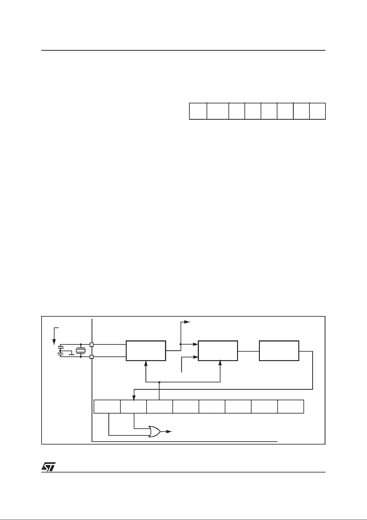
2 CENTRAL PROCESSING UNIT
2.1 INTRODUCTION
The CPUCore of ST6devices is independent ofthe
I/O or Memory configuration. As such, it may be
thought of as an independent central processor
communicating with on-chip I/O, Memory and Peripherals via internal address, data, and control
buses. In-core communication is arranged as
shown in Figure 6; the controller being externally
linked to both the Reset and Oscillator circuits,
while the core islinked to the dedicated on-chip peripherals via the serial data bus and indirectly, for
interrupt purposes, through the control registers.
2.2 CPU REGISTERS
TheST6Family CPUcorefeaturessixregisters and
three pairs of flags available to the programmer.
These are described in the following paragraphs.
Accumulator (A). The accumulator is an 8-bit
general purpose register used in all arithmetic calculations, logical operations, and data manipulations. The accumulator can be addressed in Data
space as a RAM location at address FFh. Thus the
ST6 can manipulate the accumulator just like any
other register in Data space.
Indirect Registers (X, Y).These two indirect registers are used as pointers to memory locations in
Data space. They are used in the register-indirect
addressing mode. These registers can be addressed in the data space as RAM locations at addresses 80h (X) and 81h (Y). They can also be accessed with the direct, short direct, or bit direct addressing modes. Accordingly, the ST6 instruction
set can use the indirect registers as any other register of the data space.
Short Direct Registers (V, W). These two registers are used to save a byte in short direct addressing mode. They can be addressed in Data
space as RAM locations at addresses 82h (V) and
83h (W). They can also be accessed using the direct and bit direct addressing modes. Thus, the
ST6 instruction set can use the short direct registers as any other register of the data space.
Program Counter (PC). The program counter is a
12-bit register which contains the address of the
next ROM location to be processed by the core.
This ROM location may be an opcode, an operand, or the address of an operand. The 12-bit
length allows the direct addressing of 4096 bytes
in Program space.
Figure 6. ST6 Core Block Diagram
PROGRAM
RESET
OPCODE
FLAG
VALUES
2
CONTROLLER
FLAGS
ALU
A-DATA
B-DATA
ADDRESS/READ LINE
DATA SPACE
INTERRUPTS
DATA
RAM/EEPROM
DATA
ROM/EPROM
RESULTS TO DATA SPACE (WRITE LINE)
ROM/EPROM
DEDICATIONS
ACCUMULATOR
CONTROL
SIGNALS
OSCin
OSCout
ADDRESS
DECODER
256
12
Program Counter
and
6 LAYER STACK
0,01 TO 8MHz
VR01811
352
Page 17
17/72
ST62T46B/E46B
CPU REGISTERS (Cont’d)
However, if the program space contains more than
4096 bytes, the additional memory in program
space can be addressed by using the Program
Bank Switch register.
The PC value is incremented after reading the address of the current instruction. To execute relative
jumps, the PC and the offset are shifted through
the ALU, where they are added; the result is then
shifted back into the PC. The program counter can
be changed in the following ways:
- JP (Jump) instructionPC=Jump address
- CALL instructionPC= Call address
- Relative Branch Instruction.PC= PC +/- offset
- Interrupt PC=Interrupt vector
- Reset PC= Reset vector
- RET & RETI instructionsPC= Pop (stack)
- Normal instructionPC= PC + 1
Flags (C, Z). The ST6 CPU includes three pairs of
flags (Carry and Zero), each pair being associated
with one of the three normal modes of operation:
Normal mode, Interrupt mode and Non Maskable
Interrupt mode. Each pair consists of a CARRY
flag and a ZERO flag. One pair (CN, ZN) is used
during Normal operation, another pair is used during Interrupt mode (CI, ZI), and a third pair is used
in the Non Maskable Interrupt mode (CNMI, ZNMI).
The ST6 CPU uses the pair of flags associated
with the current mode: as soon as an interrupt (or
a Non Maskable Interrupt) is generated, the ST6
CPU uses the Interrupt flags (resp. the NMI flags)
instead of the Normal flags. When the RETI instruction is executed, the previously used set of
flags is restored. It should be noted that each flag
set can only be addressed in its own context (Non
Maskable Interrupt, Normal Interrupt or Main routine). The flags are not cleared during context
switching and thus retain their status.
The Carry flag is set when a carry or a borrow occurs during arithmetic operations; otherwise it is
cleared. The Carry flag is also set to the value of
the bit tested in a bit test instruction; it also participates in the rotate left instruction.
The Zero flag is set if the result of the last arithmetic or logical operation was equal to zero; otherwise it is cleared.
Switching between the three sets of flags is performed automatically when an NMI, an interrupt or
a RETI instructions occurs. As the NMI mode is
automatically selected after the reset of the MCU,
the ST6 core uses at first the NMI flags.
Stack. The ST6 CPU includes a true LIFO hardware stack which eliminates the need for a stack
pointer. The stack consists of six separate 12-bit
RAM locations that do not belong to the data
space RAM area. When a subroutine call (or interrupt request) occurs, the contents of each level are
shifted into the next higher level, while the content
of the PC is shifted into the first level (the original
contents of the sixth stack level are lost). When a
subroutine or interrupt return occurs (RET or RETI
instructions), the first level register is shifted back
into the PC and the value of each level is popped
back into the previous level. Since the accumulator, in common with all other data space registers,
is not stored in this stack, management of these
registers should be performed within the subroutine. The stack will remain in its “deepest” position
if more than 6 nested calls or interrupts are executed, and consequently the last return address will
be lost. It will also remain in its highest position if
the stack is empty and a RET or RETI is executed.
In this case the next instruction will be executed.
Figure 7. ST6 CPU Programming Mode
l
SHORT
DIRECT
ADDRESSING
MODE
V REGISTER
WREGISTER
PROGRAM COUNTER
SIX LEVELS
STACK REGISTER
CZNORMAL FLAGS
INTERRUPTFLAGS
NMI FLAGS
INDEX
REGISTER
VA000423
b7
b7
b7
b7
b7
b0
b0
b0
b0
b0
b0b11
ACCUMULATOR
YREG.POINTER
XREG.POINTER
CZ
CZ
353
Page 18

18/72
ST62T46B/E46B
3 CLOCKS, RESET, INTERRUPTS AND POWER SAVING MODES
3.1 CLOCK SYSTEM
3.1.1 Main Oscillator
The MCU features a Main Oscillator which can be
driven by an external clock, or used in conjunction
with an AT-cut parallel resonant crystal or a suitable ceramic resonator.
Figure 8 illustrates various possible oscillator configurations using anexternal crystalorceramic resonator, an external clock input. CL1an CL2should
have a capacitance in the range 12 to 22 pF for an
oscillator frequency in the 4-8 MHz range.
The internal MCU clock Frequency (F
INT
) is divided by 13 to drive the CPU core and by 12 to drive
the A/D converter and the watchdog timer, while
clock used to drive on-chip peripherals depends
on the peripheral as shown in the clock circuit
block diagram.
With an 8MHz oscillator frequency, the fastest machine cycle is therefore 1.625µs.
A machine cycleis the smallest unit oftime needed
toexecute any operation (forinstance, toincrement
the Program Counter). An instruction may require
two, four, or five machine cycles for execution.
Figure 8. Oscillator Configurations
Figure 9. Clock Circuit Block Diagram
OSC
in
OSC
out
C
L1n
C
L2
ST6xxx
CRYSTAL/RESONATOR CLOCK
OSC
in
OSC
out
ST6xxx
EXTERNAL CLOCK
NC
VA0016
VA0015A
MAIN
OSCILLATOR
Core
:13
:12
Timer 1 & 2
Watchdog
POR
f
INT
ADC
OSCin
OSCout
f
OSC
f
INT
OSC32in
OSC32out
32kHz
OSCILLATOR
MUX
LCD
CONTROLLER
DRIVER
EOCR bit 5
(START/STOP)
354
Page 19
19/72
ST62T46B/E46B
CLOCK SYSTEM (Cont’d)
3.1.2 32 KHz STAND-BY OSCILLATOR
An additional 32KHz stand-by on chip oscillator allows to generate real time interrupts and to supply
the clock to the LCD driver with the main oscillator
stopped. This enables the MCU to perform real
time functions with the LCD display running while
keeping advantages of low power consumption.
Figure 10 shows the 32KHz oscillator block diagram.
A 32.768KHz quartz crystal must be connected to
the OSC32in and OSC32out pins to perform the
real time clock operation. Two external capacitors
of 15-22pF each must be connected between the
oscillator pins and ground. The 32KHz oscillator is
managed by the dedicated status/control register
32OCR.
As long as the 32KHz stand-by oscillator is enabled, 32KHz internal clock is available to drive
LCD controller driver. This clock is divide by 214to
generate interrupt request every 500ms . The periodic interrupt request serves as reference timebase for real time functions.
Note
: When the 32KHz stand-by oscillator is
stopped (bit 5 of the Status/Control register
cleared) the divider chain is supplied with a clock
signal synchronous with machine cycle (f
INT
/13),
this produces an interrupt request every 13x2
14
clock cycle (i.e. 26.624ms) with an 8MHz quartz
crystal.
32KHz Oscillator Register (32OCR)
Address: DBh - Read/Write
Bit 7 =EOSCI.
Enable Oscillator Interrupt
. This bit,
when set, enables the 32KHz oscillator interrupt
request.
Bit 6 = OSCEOC.
Oscillator Interrupt Flag
. This bit
indicates when the 32KHz oscillator has measured
a 500ms elapsed time (providing a
32.768KHzquartz crystal is connected to the
32KHz oscillator dedicated pins). An interrupt request can be generated in relation to the state of
EOSCI bit. This bit must be cleared by the user
program before leaving the interrupt service routine.
Bit 5 =
START/STOP
.O
scillator Start/Stop bit
.
This bit, when set, enables the 32KHz stand-by
oscillator and the free running divider chain is supplied by the 32KHz oscillator signal. When this bit
is cleared to zero the divider chain is supplied with
f
INT
/13.
This register is cleared during reset.
Note
:
To achieve minimum power consumption in STOP
mode (no system clock), the stand-by oscillator
must be switched off (real time function not available) by clearing the Start/Stop bit in the oscillator
status/control register.
Figure 10. 32KHz Oscillator Block Diagram
70
EOSCI OSCEOC S/S D4 D3 D2 D1 D0
OSC32KHz
EOSCI OSCEOC
START
STOP
XX XXX
INT
OSC32IN
OSC32OUT
2x15...22pF
32.768KHz
Crystal
f
INT
/13
OSC32KHz MUX
1
0
DIV 2
14
355
Page 20

20/72
ST62T46B/E46B
3.2 RESETS
The MCU can be reset in three ways:
– by the external Reset input being pulled low;
– by Power-on Reset;
– by the digital Watchdog peripheral timing out.
3.2.1 RESET Input
The RESET pin may be connected to a device of
the application board in order to reset the MCU if
required. The RESET pin may be pulled low in
RUN, WAIT or STOP mode. This input can be
used to reset the MCU internal state and ensure a
correct start-up procedure. The pin is active low
and features a Schmitt trigger input. The internal
Reset signal is generated by adding a delay to the
external signal. Therefore even short pulses on
the RESET pin are acceptable, provided VDDhas
completed its rising phase and that the oscillator is
running correctly (normal RUN or WAIT modes).
The MCU is kept in the Reset state as long as the
RESET pin is held low.
If RESET activation occurs in the RUN or WAIT
modes, processing of the user program is stopped
(RUN mode only), the Inputs and Outputs are configured as inputs with pull-up resistors and the
main Oscillator is restarted. When the level on the
RESET pin then goes high, the initialization sequence is executed following expiry of the internal
delay period.
If RESET pin activation occurs in the STOP mode,
the oscillator starts up and all Inputs and Outputs
are configured as inputs with pull-up resistors.
When the level of theRESET pin then goes high,
the initialization sequence is executed following
expiry of the internal delay period.
3.2.2 Power-on Reset
The function of the POR circuit consists in waking
up the MCU at an appropriate stage during the
power-on sequence. At the beginning of this sequence, the MCU is configured in the Reset state:
all I/O ports are configured as inputs with pull-up
resistors and no instruction is executed. When the
power supply voltage rises to a sufficient level, the
oscillator starts to operate, whereupon an internal
delay is initiated, in order to allow the oscillator to
fully stabilize before executing the first instruction.
The initialization sequence is executed immediately following the internal delay.
The internal delay is generated by an on-chip counter.The internal reset line is released 2048internal
clock cycles after release of the external reset.
Notes:
To ensure correct start-up, the user should take
care that the reset signal is not released before the
VDDlevel is sufficient to allow MCU operation at
the chosen frequency (see Recommended Operating Conditions).
A proper reset signal for a slow rising VDDsupply
can generally be provided by an external RC network connected to theRESET pin.
Figure 11.Reset and Interrupt Processing
INT LATCH CLEARED
NMI MASK SET
RESET
( IF PRESENT )
SELECT
NMI MODE FLAGS
IS RESET STILL
PRESENT?
YES
PUT FFEH
ON ADDRESS BUS
FROM RESET LOCATIONS
FFE/FFF
NO
FETCH INSTRUCTION
LOAD PC
VA000427
356
Page 21

21/72
ST62T46B/E46B
RESETS (Cont’d)
3.2.3 Watchdog Reset
The MCU provides a Watchdog timer function in
order to ensure graceful recovery from software
upsets. If the Watchdog register is not refreshed
before an end-of-count condition is reached, the
internal reset will be activated. This, amongst other things, resets the watchdog counter.
The MCU restarts just as though the Reset had
been generated by the RESET pin, including the
built-in stabilisation delay period.
3.2.4 Application Notes
No external resistor is required between VDDand
the Reset pin, thanks to the built-in pull-up device.
The POR circuit operates dynamically, in that it
triggers MCU initialization on detecting the rising
edge of VDD. The typical threshold is in the region
of 2 volts, but the actual value of the detected
threshold depends on the way in which VDDrises.
The POR circuit is
NOT
designed to supervise
static, or slowly rising or falling VDD.
3.2.5 MCU Initialization Sequence
When a reset occurs the stack is reset, the PC is
loaded with the address of the Reset Vector (located in program ROM starting at address 0FFEh). A
jump to the beginning of the user program must be
coded at this address. Following a Reset, the Interrupt flag is automatically set, so that the CPU is
in Non Maskable Interrupt mode; this prevents the
initialisation routine from being interrupted. The initialisation routine should therefore be terminated
by a RETI instruction, in order to revert to normal
mode and enable interrupts. If no pending interrupt
is present at the end of the initialisation routine, the
MCU will continue by processing the instruction
immediately following the RETI instruction. If, however, a pending interrupt is present, it will be serviced.
Figure 12.Reset and Interrupt Processing
Figure 13. Reset Block Diagram
RESET
RESET
VECTOR
JP
JP:2 BYTES/4 CYCLES
RETI
RETI: 1 BYTE/2 CYCLES
INITIALIZATION
ROUTINE
VA00181
V
DD
RESET
300kΩ
2.8kΩ
POWER
WATCHDOG RESET
CK
COUNTER
RESET
ST6
INTERNAL
RESET
f
OSC
RESET
ON RESET
VA0200B
357
Page 22

22/72
ST62T46B/E46B
RESETS (Cont’d)
Table 5. Register Reset Status
Register Address(es) Status Comment
EEPROM Control Register
Port Data Registers
Port A,B Direction Register
Port A,B Option Register
Interrupt Option Register
SPI Registers
LCD Mode Control Register
32kHz Oscillator Register
0DFh
0C0h, 0C2h, 0C3h
0C4h to0C5h
0CCh, 0CEh
0C8h
0C2h to0DDh
0DCh
0DBh
00h
EEPROM enabled
I/O are Input with pull-up
Interrupt disabled
SPI disabled
LCD display off
Interrupt disabled
Port C Direction Register
Port C Option Register
0C6h
0CFh
FFh LCD Output
X, Y,V, W, Register
Accumulator
Data RAM
Data RAM Page REgister
Data ROM Window Register
EEPROM
A/D Result Register
080H TO083H
0FFh
084h to0BFh
0CBh
0C9h
00h to 03Fh
0D0h
Undefined As written if programmed
TIMER 1 Status/Control
TIMER 1 Counter Register
TIMER 1 Prescaler Register
TIMER 2 Status/Control
TIMER 2 Counter Register
TIMER 2 Prescaler Register
Watchdog Counter Register
A/D Control Register
0D4h
0D3h
0D2h
0D7h
0D5h
0D6h
0D8h
0D1h
00h
FFh
7Fh
00h
FFh
7Fh
FEh
40h
TIMER 1 disabled/Max count loaded
TIMER 2 disabled/Max count loaded
A/D in Standby
358
Page 23

23/72
ST62T46B/E46B
3.3 DIGITAL WATCHDOG
The digital Watchdog consists of a reloadable
downcounter timer which can be used to provide
controlled recovery from software upsets.
The Watchdog circuit generates a Reset when the
downcounter reaches zero. User software can
prevent this reset by reloading the counter, and
should therefore be written so that the counter is
regularly reloaded while the user program runs
correctly. In the event ofa software mishap (usually caused by externally generated interference),
the user program will no longer behave in its usual
fashion and the timer register will thus not be reloaded periodically. Consequently the timer will
decrement down to 00h and reset the MCU. In order to maximise the effectiveness of the Watchdog
function, user software must be written with this
concept in mind.
Watchdog behaviour is governed by one option,
known as “WATCHDOG ACTIVATION” (i.e.
HARDWARE or SOFTWARE) (SeeTable 6).
In the SOFTWARE option, the Watchdog is disabled until bit C of the DWDR register has been set.
When the Watchdog is disabled, low power Stop
mode is available. Once activated, the Watchdog
cannot be disabled, except by resetting the MCU.
In the HARDWARE option, the Watchdog is permanently enabled. Since the oscillatorwill run continuously, low power mode is not available. The
STOP instruction is interpreted as a WAIT instruction, and the Watchdog continues to countdown.
When theMCU exits STOP mode (i.e. when an interrupt is generated), the Watchdog resumes its
activity.
Table 6. Recommended Option Choices
FunctionsRequired Recommended Options
Stop Mode “SOFTWARE WATCHDOG”
Watchdog “HARDWARE WATCHDOG”
359
Page 24

24/72
ST62T46B/E46B
DIGITAL WATCHDOG(Cont’d)
The Watchdog is associated with a Data space
register (Digital WatchDog Register, DWDR, location 0D8h) which is described in greater detail in
Section 3.3.1 Digital Watchdog Register (DWDR).
This register is set to 0FEh on Reset: bit C is
cleared to “0”, which disables the Watchdog; the
timer downcounter bits, T0 to T5, and the SR bit
are all set to “1”, thus selecting the longest Watchdog timer period. This time period can be set to the
user’s requirements by setting the appropriate value for bits T0 to T5 in the DWDR register. The SR
bit must be set to “1”, since it is this bit which generates the Reset signal when it changes to “0”;
clearing this bit would generate an immediate Reset.
It should be noted that the order of the bits in the
DWDR register is inverted with respect to the associated bits in the down counter: bit 7 of the
DWDR register corresponds, in fact, to T0 and bit
2 to T5. The user should bear in mind the fact that
these bits are inverted and shifted with respect to
the physical counter bits when writing to this register. The relationship between the DWDR register
bits and the physical implementation of the Watchdog timer downcounter is illustrated inFigure 14.
Only the 6 most significant bits may be used to define the time period, since it is bit 6 which triggers
the Reset when it changes to “0”. This offers the
user a choice of 64 timed periods ranging from
3,072 to 196,608 clock cycles (with an oscillator
frequency of 8MHz, this is equivalent to timer periods ranging from 384µs to 24.576ms).
Figure 14.Watchdog Counter Control
WATCHDOG CONTROL REGISTER
D0
D1
D3
D4
D5
D6
D7
WATCHDOG COUNTER
C
SR
T5
T4
T3
T2
T1
D2
T0
OSC÷12
RESET
VR02068A
÷
2
8
360
Page 25

25/72
ST62T46B/E46B
DIGITAL WATCHDOG(Cont’d)
3.3.1 Digital Watchdog Register (DWDR)
Address: 0D8h — Read/Write
Reset status: 1111 1110b
Bit 0 = C:
Watchdog Control bit
If the hardware option is selected, this bit is forced
high and the user cannot change it (the Watchdog
is always active). When the software option is selected, the Watchdog function is activated by setting bit C to 1, and cannot then be disabled (save
by resetting the MCU).
When C is kept low the counter can be used as a
7-bit timer.
This bit is cleared to “0” on Reset.
Bit 1 =SR:
Software Reset bit
This bit triggers a Reset when cleared.
When C = “0” (Watchdog disabled) it is the MSB of
the 7-bit timer.
This bit is set to “1” on Reset.
Bits 2-7 = T5-T0:
Downcounter bits
It should be noted that the register bits are reversed and shifted with respect to the physical
counter: bit-7 (T0) is the LSB of the Watchdog
downcounter and bit-2 (T5) is the MSB.
These bits are set to “1” on Reset.
3.3.2 Application Notes
The Watchdog plays an important supporting role
in the high noise immunity of ST62xx devices, and
should be used wherever possible. Watchdog related options should be selected on the basis of a
trade-off between application security and STOP
mode availability.
When STOP mode is not required, hardware activation should be preferred, as it provides maximum security, especially during power-on.
When software activation is selected and the
Watchdog is not activated, the downcounter may
be used as a simple 7-bit timer (remember that the
bits are in reverse order).
The software activation option should be chosen
only when the Watchdog counter is to be used as
a timer. To ensure the Watchdog has not been unexpectedly activated, the following instructions
should be executed within the first 27 instructions:
jrr 0, WD, #+3
ldi WD, 0FDH
70
T0 T1 T2 T3 T4 T5 SR C
361
Page 26

26/72
ST62T46B/E46B
DIGITAL WATCHDOG(Cont’d)
These instructions test the C bit and Reset the
MCU (i.e. disable the Watchdog) if the bit is set
(i.e. if the Watchdog is active), thus disabling the
Watchdog.
In all modes, a minimum of 28 instructions are executed after activation, before the Watchdog can
generate a Reset. Consequently, user software
should load the watchdog counter within the first
27 instructions following Watchdog activation
(software mode), or within the first 27 instructions
executed following a Reset (hardware activation).
It should be noted that when the GEN bit is low (interrupts disabled), the NMI interrupt is active but
cannot cause a wake up from STOP/WAIT modes.
Figure 15. Digital Watchdog Block Diagram
RSFF
8
DATA BUS
VA00010
-2
-12
OSCILLATOR
RESET
WRITE
RESET
DB0
R
S
Q
DB1.7 SETLOAD
7
8
-2
SET
CLOCK
362
Page 27

27/72
ST62T46B/E46B
3.4 INTERRUPTS
The CPU can manage four Maskable Interrupt
sources, in addition to a Non Maskable Interrupt
source (top priority interrupt). Each source is associated with a specific Interrupt Vector which contains a Jump instruction to the associated interrupt
service routine. These vectors are located in Program space (seeTable 7).
When an interrupt source generates an interrupt
request, and interrupt processing is enabled, the
PC register is loaded with the address of the interrupt vector (i.e. of the Jump instruction), which
then causes a Jump to the relevant interrupt service routine, thus servicing the interrupt.
Interrupt sources are linked to events either on external pins, or on chip peripherals. Several events
can be ORed on the same interrupt source, and
relevant flags are available to determine which
event triggered the interrupt.
The Non Maskable Interrupt request has the highest priority and can interrupt any interrupt routine
at any time; the other four interrupts cannot interrupt each other. If more than one interrupt request
is pending, these are processed by the processor
core according to their priority level: source #1 has
the higher priority while source #4 the lower. The
priority of each interrupt source is fixed.
Table 7. Interrupt Vector Map
3.4.1 Interrupt request
All interrupt sources but the Non Maskable Interrupt source can be disabled by setting accordingly
the GEN bit of the Interrupt Option Register (IOR).
This GEN bit also defines if an interrupt source, including the Non Maskable Interrupt source, can restart the MCU from STOP/WAIT modes.
Interrupt request from the Non Maskable Interrupt
source #0is latched by a flip flop which is automat-
ically reset by the core at the beginning of the nonmaskable interrupt service routine.
Interrupt request from source #1 can be configured either as edge or level sensitive by setting accordingly the LES bit of the Interrupt Option Register (IOR).
Interrupt request from source #2 are always edge
sensitive. The edge polarity can be configured by
setting accordingly the ESB bit of the Interrupt Option Register (IOR).
Interrupt request from sources #3 & #4 are level
sensitive.
In edge sensitive mode, a latch is set when a edge
occurs on the interrupt source line and is cleared
when the associated interrupt routine is started.
So, the occurrence of an interrupt can be stored,
until completion of the running interrupt routine before being processed. If several interrupt requests
occurs before completion of the running interrupt
routine, only the first request is stored.
Storage ofinterrupt requests is not available inlevel sensitive mode. To be taken into account, the
low level must be present on the interrupt pinwhen
the MCU samples the line after instruction execution.
At the end of every instruction, the MCU tests the
interrupt lines: if there is an interrupt request the
next instruction is not executed and the appropriate interrupt service routine is executed instead.
Table 8. Interrupt Option Register Description
Interrupt Source Priority Vector Address
Interrupt source #0 1 (FFCh-FFDh)
Interrupt source #1 2 (FF6h-FF7h)
Interrupt source #2 3 (FF4h-FF5h)
Interrupt source #3 4 (FF2h-FF3h)
Interrupt source #4 5 (FF0h-FF1h)
GEN
SET Enable all interrupts
CLEARED Disable all interrupts
ESB
SET
Rising edge mode on interrupt source #2
CLEARED
Falling edge mode on interrupt source #2
LES
SET
Level-sensitive mode on interrupt source #1
CLEARED
Falling edge mode on interrupt source #1
OTHERS NOT USED
363
Page 28

28/72
ST62T46B/E46B
INTERRUPTS (Cont’d)
3.4.2 Interrupt Procedure
The interrupt procedure is very similar to a call procedure, indeed the user can consider the interrupt
as an asynchronous call procedure. As this is an
asynchronous event, the user cannot know the
context and the time at which it occurred. As a result, the user should save all Data space registers
which may be used within the interrupt routines.
There are separate sets of processor flags for normal, interrupt and non-maskable interrupt modes,
which are automatically switched and so do not
need to be saved.
The following list summarizes the interrupt procedure:
MCU
– The interrupt is detected.
– The C and Z flags are replaced by the interrupt
flags (or by the NMI flags).
– The PC contents are stored in the first level of
the stack.
– The normal interrupt lines are inhibited (NMI still
active).
– The first internal latch is cleared.
–Theassociatedinterruptvectorisloaded inthePC.
WARNING: In some circumstances, when a
maskable interrupt occurs while the ST6 core is in
NORMAL mode and especially during the execution of an ”ldi IOR, 00h” instruction (disabling all
maskable interrupts): if the interrupt arrives during
the first 3 cycles of the ”ldi” instruction (which is a
4-cycle instruction) the core will switch to interrupt
mode BUT the flags CN and ZN will NOT switch to
the interrupt pair CI and ZI.
User
– User selected registers are saved within the in-
terrupt service routine (normally on a software
stack).
– The source of the interrupt is found by polling the
interrupt flags (if more than one source is associ-
ated with the same vector).
– The interrupt is serviced.
– Return from interrupt (RETI)
MCU
– Automatically the MCU switches back to the nor-
mal flag set (or the interrupt flag set) and pops
the previous PC value from the stack.
The interrupt routine usually begins by the identifying the device which generated the interrupt request (by polling). The user should save the registers which are used within the interrupt routine in a
software stack. After the RETI instruction is executed, the MCU returns to the main routine.
Figure 16.Interrupt Processing Flow Chart
INSTR UCTION
FETCH
INSTR UCTION
EXECUT E
INSTRUCTIO N
WAS
THE INS TRUCTION
ARETI ?
?
CLEAR
INTER RUPT MASK
SELECT
PROGRAM FLAGS
”POP”
THE STACKED PC
?
CHE CK IF THERE IS
AN INTERRUPT RE QUEST
AND INTERRUPT MASK
SELECT
INTERNAL MODE FLAG
PUSH THE
PC INTO THE STACK
LOAD PC FROM
INTERR UPT VECTOR
(FFC/FFD )
SET
INTER RUPT MASK
NO
NO
YES
IS THE CORE
ALREADY IN
NORMAL MODE?
VA000014
YES
NO
YES
364
Page 29

29/72
ST62T46B/E46B
INTERRUPTS (Cont’d)
3.4.3 Interrupt Option Register (IOR)
The Interrupt Option Register (IOR) is used to enable/disable the individual interrupt sources and to
select the operating mode of the external interrupt
inputs. This register is write-only and cannot be
accessed by single-bit operations.
Address: 0C8h — Write Only
Reset status: 00h
Bit 7, Bits 3-0 =
Unused
.
Bit 6 = LES:
Level/Edge Selection bit
.
When this bit is set to one, the interrupt source #1
is level sensitive. When cleared to zero the edge
sensitive mode for interrupt request is selected.
Bit 5 = ESB:
Edge Selection bit
.
The bit ESB selects the polarity of the interrupt
source #2.
Bit 4 =GEN:
Global Enable Interrupt
. When this bit
is set to one, all interrupts are enabled. When this
bit is cleared to zero all the interrupts (excluding
NMI) are disabled.
When the GEN bit is low, the NMI interrupt is active but cannot cause a wake up from STOP/WAIT
modes.
This register is cleared on reset.
3.4.4 Interrupt Sources
Interrupt sources available on the
ST62E46B/T40B are summarized in theTable 9
with associated mask bit to enable/disable the interrupt request.
Table 9. Interrupt Requests and Mask Bits
70
- LES ESB GEN - - - -
Peripheral Register
Address
Register
Mask bit Masked Interrupt Source
Interrupt
source
GENERAL IOR C8h GEN
All Interrupts, excluding NM
I All
TIMER 1
TIMER 2
TSCR1
TSCR2
D4h
D7h
ETI TMZ: TIMER Overflow source 3
A/D CONVERTER ADCR D1h EAI EOC: End of Conversion source 4
SPI SPI C2h ALL End of Transmission source 1
Port PAn ORPA-DRPA C0h-C4h ORPAn-DRPAn PAnpin source 2
Port PBn ORPB-DRPB C1h-C5h ORPBn-DRPBn PBn pin source 2
Port PCn ORPC-DRPC C6h-CFh ORPCn-DRPCn PCn pin source 2
PSS PSSCR DAh PEI PIF: source 0
32kHz OSC 32OCR DBh EOSCI OSCEOC source 3
365
Page 30

30/72
ST62T46B/E46B
INTERRUPTS (Cont’d)
Figure 17. Interrupt Block Diagram
PORT A
PBE
V
DD
FROM REGISTER PORT A,B,C
SINGLE BIT ENABLE
FF
CLK Q
CLR
I
0
Start
INT #0 NMI (FFC,D))
INT #2 (FF4,5)
NMI
PORT B
Bits
SPI
FF
CLK Q
CLR
0
MUX
1
I
1
Start
IOR bit 6 (LES)
PBE
FF
CLK Q
CLR
IOR bit 5 (ESB)
I
2
Start
INT #1 (FF6,7)
INT #3 (FF2,3)
INT #4 (FF0,1)
IOR bit 4(GEN)
PORT C
TMZ
ETI
TMZ
ETI
OSCEOC
EOSCI
EAI
EOC
RESTART
STOP/WAIT
FROM
PBE
PIF
PEI
TIMER1
TIMER2
OSC32kHz
A/D CONVERTER
PSS
366
Page 31

31/72
ST62T46B/E46B
3.5 POWER SAVING MODES
The WAIT and STOP modes have been implemented in the ST62xx family of MCUs in order to
reduce the product’s electrical consumption during
idle periods. These two power saving modes are
described in the following paragraphs.
3.5.1 WAIT Mode
The MCU goes into WAIT mode as soon as the
WAIT instruction is executed. The microcontroller
can be considered as being in a “software frozen”
state where the core stops processing the program instructions, the RAM contents and peripheral registers are preserved as long as the power
supply voltage is higher than the RAM retention
voltage. In this mode the peripherals are still active.
WAIT mode can be used when the user wants to
reduce the MCU power consumption during idle
periods, while not losing track of time or the capability of monitoring external events. The active oscillator is not stopped in order to provide a clock
signal to the peripherals. Timer counting may be
enabled as well as the Timer interrupt, before entering the WAIT mode: this allows the WAIT mode
to be exited when a Timer interrupt occurs. The
same applies to other peripherals which use the
clock signal.
If the WAIT mode is exited due to a Reset (either
by activating the external pin or generated by the
Watchdog), the MCU enters a normal reset procedure. If an interrupt is generated during WAIT
mode, the MCU’s behaviour depends on the state
of the processor core prior to the WAIT instruction,
but also on the kind of interrupt request which is
generated. This is described in the following paragraphs. The processor core does not generate a
delay following the occurrence of the interrupt, because the oscillator clock is still available and no
stabilisation period is necessary.
3.5.2 STOP Mode
If the Watchdog isdisabled, STOP mode is available. When in STOP mode, the MCU is placed in
the lowest power consumption mode. In this operating mode, the microcontroller can be considered
as being “frozen”, no instruction is executed, the
oscillator is stopped, the RAM contents and peripheral registers are preserved as long as the
power supply voltage is higher than the RAM retention voltage, and the ST62xx core waits for the
occurrence of an external interrupt request or a
Reset to exit the STOP state.
If the STOP state is exited due to a Reset (by activating the external pin) the MCU will enter a normal reset procedure. Behaviour in response to interrupts depends on the state of the processor
core prior to issuing the STOP instruction, and
also on the kind of interrupt request that is generated.
This case will be described in the following paragraphs. The processor core generates a delay after occurrence of the interrupt request, in order to
wait for complete stabilisation of the oscillator, before executing the first instruction.
367
Page 32

32/72
ST62T46B/E46B
POWER SAVING MODE(Cont’d)
3.5.3 Exit from WAIT and STOP Modes
The following paragraphs describe how the MCU
exits from WAIT and STOP modes, when an interrupt occurs (not a Reset). It should be noted that
the restart sequence depends on the original state
of the MCU (normal, interrupt or non-maskable interrupt mode) prior to entering WAIT or STOP
mode, as well as on the interrupt type.
Interrupts do not affect the oscillator selection.
3.5.3.1 Normal Mode
If the MCU was in the main routine when the WAIT
or STOP instruction was executed, exit from Stop
or Wait mode will occur as soon as an interrupt occurs; the related interrupt routine is executed and,
on completion, the instruction which follows the
STOP or WAIT instruction is then executed, providing no other interrupts are pending.
3.5.3.2 Non Maskable Interrupt Mode
If the STOP or WAIT instruction has been executed during execution of the non-maskable interrupt
routine, the MCU exits from the Stop or Wait mode
as soon as an interrupt occurs: the instruction
which follows the STOP or WAIT instruction is executed, and the MCU remains in non-maskable interrupt mode, even if another interrupt has been
generated.
3.5.3.3 Normal Interrupt Mode
If the MCU was in interrupt mode before the STOP
or WAIT instruction was executed, it exits from
STOP or WAIT mode as soon as an interrupt occurs. Nevertheless, two cases must be considered:
– If the interrupt is a normal one, the interrupt rou-
tine in which the WAIT or STOP mode was en-
tered will be completed, starting with the
execution of the instruction which follows the
STOP or the WAIT instruction, and the MCU is
still in the interrupt mode. At the end of this routine pending interrupts will be serviced in accordance with their priority.
– In the event of a non-maskable interrupt, the
non-maskable interrupt service routine is processed first, then the routine in which the WAIT or
STOP mode was entered will be completed by
executing the instruction following the STOP or
WAIT instruction. The MCU remains in normal
interrupt mode.
Notes:
To achieve the lowest power consumption during
RUN or WAIT modes, the user program must take
care of:
– configuring unused I/Os asinputswithout pull-up
(these should be externally tied to well defined
logic levels);
– placing all peripherals in their power down
modes before entering STOP mode;
When the hardware activated Watchdog is selected, or when the software Watchdog is enabled, the
STOP instruction is disabled and a WAIT instruction will be executed in its place.
If all interrupt sources are disabled (GEN low), the
MCU can only be restarted by a Reset. Although
setting GEN low does not mask the NMI as an interrupt, it will stop it generating a wake-up signal.
The WAIT and STOP instructions are not executed if an enabled interrupt request is pending.
368
Page 33

33/72
ST62T46B/E46B
4 ON-CHIP PERIPHERALS
4.1 I/O PORTS
The MCU features Input/Output lines which may
be individually programmed as any of the following
input or output configurations:
– Input without pull-up or interrupt
– Input with pull-up and interrupt
– Input with pull-up, but without interrupt
– Analog input
– Push-pull output
– Open drain output
The lines are organised as bytewise Ports.
Each port is associated with 3 registers in Data
space. Each bit of these registers is associated
with a particular line (for instance, bits 0 of Port A
Data, Direction and Option registers are associated with the PA0 line of Port A).
The DATA registers (DRx), are used to read the
voltage level values of the lines which have been
configured as inputs, or to write the logic value of
the signal to be output on the lines configured as
outputs. The port data registers can be read to get
the effective logic levels of the pins, but they can
be also written by user software, in conjunction
with the related option registers, to select the different input mode options.
Single-bit operations on I/O registers are possible
but care is necessary because reading in input
mode is done from I/O pins while writing will directly affect the Port data register causing an undesired change of the input configuration.
The Data Direction registers (DDRx) allow the
data direction (input or output) of each pin to be
set.
The Option registers (ORx) are used to select the
different port options available both in input and in
output mode.
All I/O registers can be read or written to just as
any other RAM location in Data space, so noextra
RAM cells are needed for port data storage and
manipulation. During MCUinitialization, all I/O registers are cleared and the input mode with pull-ups
and no interrupt generation is selected for all the
pins, thus avoiding pin conflicts.
Figure 18. I/O Port Block Diagram
V
DD
RESET
S
IN
CONTROLS
S
OUT
SHIFT
REGISTER
DATA
DATA
DIRECTION
REGISTER
REGISTER
OPTION
REGISTER
INPUT/OUTPUT
TO INTERRUPT
V
DD
TO ADC
VA00413
369
Page 34

34/72
ST62T46B/E46B
I/O PORTS (Cont’d)
4.1.1 Operating Modes
Each pin may be individually programmed as input
or output with various configurations.
This is achieved by writing the relevant bit in the
Data (DR), Data Direction (DDR) and Option registers (OR). Table 10 illustrates the various port
configurations which can be selected by user software.
4.1.1.1 Input Options
Pull-up, High Impedance Option. All input lines
can be individually programmed with or without an
internal pull-up by programming the OR and DR
registers accordingly. If the pull-up option is not
selected, the input pin will be in the high-impedance state.
4.1.1.2 Interrupt Options
All input lines can be individually connected by
software to the interrupt system by programming
the OR and DR registers accordingly. The interrupt trigger modes (falling edge, rising edge and
low level) can be configured by software as described in the Interrupt Chapter for each port.
4.1.1.3 Analog Input Options
Some pins can be configured as analog inputs by
programming the OR and DR registers accordingly. These analog inputs are connected to the onchip 8-bit Analog to Digital Converter.
ONLY ONE
pin should be programmed as an analog input at
any time, since by selecting more than one input
simultaneously their pins will be effectively shorted.
Table 10. I/O Port Option Selection
Note: X = Don’t care
DDR OR DR Mode Option
0 0 0 Input With pull-up, no interrupt
0 0 1 Input No pull-up, no interrupt
0 1 0 Input With pull-up and with interrupt
0 1 1 Input Analog input (when available)
1 0 X Output Open-drain output (20mA sink when available)
1 1 X Output Push-pull output (20mA sink when available)
370
Page 35

35/72
ST62T46B/E46B
I/O PORTS (Cont’d)
4.1.2 Safe I/O State Switching Sequence
Switching the I/O ports from one state to another
should be done in a sequence which ensures that
no unwanted side effects can occur. The recommended safe transitions are illustrated in Figure
19. All other transitions are potentially risky and
should be avoided when changing the I/O operating mode, as it is most likely that undesirable sideeffects will be experienced, such as spurious interrupt generation or two pins shorted together by the
analog multiplexer.
Single bit instructions (SET, RES, INC and DEC)
should be used with great caution on Ports Data
registers, since these instructions make an implicit
read and write back of the entire register. In port
input mode, however, the data register reads from
the input pins directly, and not from the data register latches. Since data register information in input
mode is used to set the characteristics of the input
pin (interrupt, pull-up, analog input), these may be
unintentionally reprogrammed depending on the
state of the input pins. As a general rule, it is better
to limit the use of single bit instructions on data
registers to when the whole (8-bit) port is in output
mode. In the case of inputs or of mixed inputs and
outputs, it is advisable to keep a copy of the data
register in RAM. Single bit instructions may then
be used on the RAM copy, after which the whole
copy register can be written to the port data register:
SET bit, datacopy
LD a, datacopy
LD DRA, a
Warning: Care must also be taken to not use instructions that act on a whole port register (INC,
DEC, or read operations) when all 8 bits are not
available on the device. Unavailable bits must be
masked by software (AND instruction).
The WAIT and STOP instructions allow the
ST62xx to be used in situations where low power
consumption is needed. The lowest power consumption is achieved by configuring I/Os in input
mode with well-defined logic levels.
The user must take care not to switch outputs with
heavy loads during the conversion of one of the
analog inputs in order to avoid any disturbance to
the conversion.
Figure 19. Diagram showing Safe I/O State Transitions
Note *. xxx = DDR, OR, DR Bits respectively
Interrupt
pull-up
Output
Open Drain
Output
Push-pull
Input
pull-up (Reset
state)
Input
Analog
Output
Open Drain
Output
Push-pull
Input
010*
000
100
110
011
001
101
111
371
Page 36

36/72
ST62T46B/E46B
I/O PORTS (Cont’d)
Table 11. I/O Port configuration for the ST62T46B/E46B
Note 1. Provided the correct configuration has been selected.
MODE AVAILABLE ON(1) SCHEMATIC
Input
PA4-PA7
PB0-PB7
PC0-PC7
Input
with pull up
(Reset state except for
PC0-PC7)
PA4-PA7
PB0-PB7
PC0-PC7
Input
with pull up
with interrupt
PA4-PA7
PB0-PB7
PC0-PC7
Analog Input
PA4-PA7
PB0-PB3
Open drain output
5mA
Open drain output
20mA
PA4-PA7
PB0-PB7
PC0-PC7 (1mA)
PB4-PB7
Push-pull output
5mA
Push-pull output
20mA
PA4-PA7
PB0-PB7
PC0-PC7 (1mA)
PB4-PB7
Data in
Interrupt
Data in
Interrupt
Data in
Interrupt
Data out
ADC
Data out
372
Page 37

37/72
ST62T46B/E46B
I/O PORTS (Cont’d)
4.1.3 LCD alternate functions (combiports)
PC0 to PC7 can also be individually defined as 8
LCD segment output by setting DDRC, ORC and
DRC registers as shown inTable 12.
On the contrary with other I/O lines, the reset state
is the LCDoutput mode.These 8 segment lines are
recognised as S33..S40 by the embedded LCD
controller drive.
4.1.4 SPI alternate functions
PB6/Sin and PB5/Scl pins must be configured as
input through the DDR and OR registers to be
used data in and data clock (Slave mode) for the
SPI. All input modes are available and I/O’s can be
read independantly of the SPI at any time.
PB7/Sout must be configured in open drain output
mode to be used as data out for the SPI. In output
mode, the value present on the pin is the port data
register content only if PB7 is defined as push pull
output, while serial transmission is possible only in
open drain mode.
Table 12. PC0-PC7 Combiport Option Selection
Note: X = Don’t care
Figure 20. Peripheral Interface Configuration of SPI
DDR OR DR Mode Option
0 0 0 Input With pull-up, no interrupt
0 0 1 Input No pull-up, no interrupt
0 1 0 Input With pull-up and with interrupt
0 1 1 Input LCD segment (Reset state)
1 0 X Output Open-drain output
1 1 X Output Push-pull output
PB7/Sout
PB6/Sin
PB5/Scl
PID
OPR
DR1
MUX
0
OUT
IN
SYNCHRONOUS
SERIAL I/O
CLOCK
PID
DR
PID
DR
PP/OD
VR01661F
373
Page 38

38/72
ST62T46B/E46B
I/O PORTS (Cont’d)
4.1.5 I/O Port Option Registers
ORA/B/C (CCh PA, CDh PB, CFh PC)
Read/Write
Bit 7-0 =
Px7 - Px0
:
Port A, B, C Option Register
bits.
4.1.6 I/O Port Data Direction Registers
DDRA/B/C (C4h PA, C5h PB, C6h PC)
Read/Write
Bit 7-0 = Px7 - Px0:
Port A, B, C Data Direction
Registers bits.
4.1.7 I/O Port Data Registers
DRA/B/C (C0h PA, C1h PB, C3h PC)
Read/Write
Bit 7-0 =
Px7 - Px0
:
Port A, B, C Data Registers
bits.
70
Px7 Px6 Px5 Px4 Px3 Px2 Px1 Px0
70
Px7 Px6 Px5 Px4 Px3 Px2 Px1 Px0
70
Px7 Px6 Px5 Px4 Px3 Px2 Px1 Px0
374
Page 39

39/72
ST62T46B/E46B
4.2 TIMER 1 & 2
The MCU features two on-chip Timer peripheral
named TIMER 1 & TIMER 2. Each of these timers
consist of an 8-bit counter with a 7-bit programmable prescaler, giving a maximum count of 215.
The content of the 8-bit counter can be read/written in the Timer/Counter register, TCR, while the
state of the 7-bit prescaler can be read in the PSC
register. The control logic device is managed in
the TSCR register as described in the following
paragraphs.
The 8-bit counter is decremented by the output
(rising edge) coming from the 7-bit prescaler and
can be loaded and read under program control.
When it decrements to zero then the TMZ (Timer
Zero) bit in the TSCR is set to “1”. If the ETI (Enable Timer Interrupt) bit in the TSCR is also set to
“1”, an interrupt request is generated as described
in the Interrupt Chapter. The Timer interrupt can
be used to exit the MCU from WAIT mode.
The prescaler input is the internal frequency f
INT
divided by 12 (TIMER 1 & 2). The prescaler decre-
ments on the rising edge. Depending on the division factor programmed by PS2, PS1 and PS0 bits
in the TSCR. The clock input of the timer/counter
register is multiplexed to different sources. For division factor 1, the clock input of the prescaler is
also that of timer/counter; for factor 2, bit 0 of the
prescaler register is connected to the clock input of
TCR. This bit changes its state at half the frequency of the prescaler input clock. For factor 4, bit 1 of
the PSC is connected to the clock input of TCR,
and so forth. The prescaler initialize bit, PSI, in the
TSCR register must be set to “1” to allow the prescaler (and hence the counter) to start. If it is
cleared to “0”, all the prescaler bits are set to “1”
and the counter is inhibited from counting. The
prescaler can be loaded with any value between 0
and 7Fh, if bit PSI is set to “1”. The prescaler tap is
selected by means of the PS2/PS1/PS0 bits in the
control register.
Figure 21 illustrates the Timer’s working principle.
Figure 21. Timer Working Principle
BIT0 BIT1 BIT2 BIT3 BIT6BIT5BIT4
CLOCK
7-BIT PRESCALER
8-1 MULTIPLEXER
8-BIT COUNTER
BIT0 BIT1
BIT2
BIT3 BIT4 BIT5
BIT6
BIT7
10234567
PS0
PS1
PS2
VA00186
375
Page 40

40/72
ST62T46B/E46B
Figure 22. TIMER 1 & 2 Block Diagram
DATA BUS
8-BIT
COUNTER
STATUS/CONTROL
REGISTER
INTERRUPT
LINE
VR02070A
3
8
8
8
6
5
4
3
2
1
0
SELECT
1OF7
12
b7 b6 b5 b4 b3 b2 b1 b0
TMZ ETI D5 D4 PSI PS2 PS1 PS0
f
INT
PSC
376
Page 41

41/72
ST62T46B/E46B
TIMER 1& 2 (Cont’d)
4.2.1 TIMER 1 & 2 Operating Mode
The Timer prescaler is clocked by the prescaler
clock input (f
INT
÷12).
The user can select for each TIMER the desired
prescaler division ratio through the PS2, PS1, PS0
bits. When the TCR count reaches 0, it sets the
TMZ bit in the TSCR. The TMZ bit can be tested
under program control to perform a timer function
whenever it goes high.
4.2.2 Timer Interrupt
When one of the counter registers decrements to
zero with the associated ETI (Enable Timer Interrupt) bit set to one, an interrupt request is generated as described in Interrupt Chapter. When the
counter decrements to zero, the associated TMZ
bit in the TSCR register is set to one.
4.2.3 Application Notes
TMZ is set when the counter reaches zero; however, it may also be set by writing 00h in the TCR
register or by setting bit 7 of the TSCR register.
The TMZ bit must be cleared by user software
when servicing the timer interrupt to avoid undesired interrupts when leaving the interrupt service
routine. After reset, the 8-bit counter register is
loaded with 0FFh, while the 7-bit prescaler is loaded with 07Fh, and the TSCR register is cleared.
This means that the Timer is stopped (PSI=“0”)
and the timer interrupt is disabled.
A write to the TCR register will predominate over
the 8-bit counter decrement to 00h function, i.e. if a
write and a TCR register decrement to 00h occur
simultaneously, the write will take precedence,
and the TMZ bit is not set until the 8-bit counter
reaches 00h again. The values of the TCR and the
PSC registers can be read accurately at any time.
377
Page 42

42/72
ST62T46B/E46B
TIMER 1& 2 (Cont’d)
4.2.4 TIMER 1 Registers
Timer Status Control Register (TSCR)
Address: 0D4h — Read/Write
Bit 7 = TMZ:
Timer Zero bit
A low-to-high transition indicates that the timer
count register has decrement to zero. This bit
must be cleared by user software before starting a
new count.
Bit 6 = ETI:
Enable Timer Interrup
When set, enables the timer interrupt request. If
ETI=0 the timer interrupt is disabled. If ETI=1 and
TMZ=1 an interrupt request is generated.
Bit 5 =
Reserved.
Must be set to 1.
Bit 4 = Do not care
Data sent to the timer output when TMZ is set high
(output mode only). Input mode selection (input
mode only)
Bit 3 = PSI:
Prescaler Initialize Bit
Used to initialize the prescaler and inhibit its counting. When PSI=“0” the prescaler is set to 7Fh and
the counter is inhibited. When PSI=“1” the prescaler is enabled to count downwards. As long as
PSI=“0” both counter and prescaler are not running.
Bit 2, 1, 0 = PS2, PS1, PS0:
Prescaler Mux. Se-
lect.
These bits select the division ratio of the pres-
caler register.
Table 13. Prescaler Division Factors
Timer Counter Register (TCR)
Address: 0D3h — Read/Write
Bit 7-0 = D7-D0:
Counter Bits.
Prescaler Register PSC
Address: 0D2h — Read/Write
Bit 7 = D7: Always read as ”0”.
Bit 6-0 =
D6-D0
: Prescaler Bits.
70
TMZ ETI - - PSI PS2 PS1 PS0
PS2 PS1 PS0 Divided by
0001
0012
0104
0118
10016
10132
11064
1 1 1 128
70
D7 D6 D5 D4 D3 D2 D1 D0
70
D7 D6 D5 D4 D3 D2 D1 D0
378
Page 43

43/72
ST62T46B/E46B
TIMER 1& 2 (Cont’d)
4.2.5 TIMER 2 Registers
Timer Status Control Register (TSCR)
Address: 0D7h — Read/Write
Bit 7 = TMZ:
Timer Zero bit
A low-to-high transition indicates that the timer
count register has decrement to zero. This bit
must be cleared by user software before starting a
new count.
Bit 6 = ETI:
Enable Timer Interrup
When set, enables the timer interrupt request. If
ETI=0 the timer interrupt is disabled. If ETI=1 and
TMZ=1 an interrupt request is generated.
Bit 5 = D5:
Reserved
Must be set to “1”.
Bit 4 = D4
Do not care.
Bit 3 =
PSI
:
Prescaler Initialize Bit
Used to initialize the prescaler and inhibit its counting. When PSI=“0” the prescaler is set to 7Fh and
the counter is inhibited. When PSI=“1” the prescaler is enabled to count downwards. As long as
PSI=“0” both counter and prescaler are not running.
Bit 2, 1, 0 = PS2, PS1, PS0:
Prescaler Mux. Se-
lect.
These bits select the division ratio of the pres-
caler register.
Table 14. Prescaler Division Factors
Timer Counter Register (TCR)
Address: 0D6h — Read/Write
Bit 7-0 = D7-D0:
Counter Bits.
Prescaler Register PSC
Address: 0D5h — Read/Write
Bit 7 = D7: Always read as ”0”.
Bit 6-0 =
D6-D0
: Prescaler Bits.
70
TMZ ETI D5 D4 PSI PS2 PS1 PS0
PS2 PS1 PS0 Divided by
0001
0012
0104
0118
10016
10132
11064
1 1 1 128
70
D7 D6 D5 D4 D3 D2 D1 D0
70
D7 D6 D5 D4 D3 D2 D1 D0
379
Page 44

44/72
ST62T46B/E46B
4.3 A/D CONVERTER (ADC)
The A/D converter peripheral is an 8-bit analog to
digital converter with analog inputs as alternate I/O
functions (the number of which is device dependent), offering 8-bit resolution with a typical conversion time of 70us (at an oscillator clock frequency
of 8MHz).
The ADC converts the input voltage by a process
of successive approximations, using a clock frequency derived from the oscillator with a division
factor of twelve. With an oscillator clock frequency
less than 1.2MHz, conversion accuracy is decreased.
Selection of the input pin is done by configuring
the related I/O line as an analog input via the Option and Data registers (refer to I/O ports description for additional information). Only one I/O line
must be configured as an analog input atany time.
The user must avoid any situation in which more
than one I/O pin is selected as an analog input simultaneously, to avoid device malfunction.
The ADC uses two registers in the data space: the
ADC data conversion register, ADR, which stores
the conversion result, and the ADC control register, ADCR, used to program the ADC functions.
A conversion is started by writing a “1” to the Start
bit (STA) in the ADC control register. This automatically clears (resets to “0”) the End Of Conversion Bit (EOC). When a conversion is complete,
the EOC bit is automatically set to “1”, in order to
flag that conversion is complete and that the data
in the ADC data conversion register is valid. Each
conversion has to be separately initiated by writing
to the STA bit.
The STA bit is continuously scanned so that, if the
user sets it to “1” while a previous conversion is in
progress, a new conversion is started before completing the previous one. The start bit (STA) is a
write only bit, any attempt to read it will show a logical “0”.
The A/D converter features a maskable interrupt
associated with the end of conversion. This interrupt is associated with interrupt vector #4 and occurs when the EOC bit is set (i.e. when a conversion is completed). The interrupt is masked using
the EAI (interrupt mask) bit in the control register.
The power consumption of the device can be reduced by turning off the ADC peripheral. This is
done by setting the PDS bit in the ADC control register to “0”. If PDS=“1”, the A/D is powered and enabled for conversion. This bit must be set at least
one instruction before the beginning of the conver-
sion to allow stabilisation of the A/D converter.
This action is also needed before entering WAIT
mode, since the A/D comparator is not automatically disabled in WAIT mode.
During Reset, any conversion in progress is
stopped, thecontrolregister is reset to 40h and the
ADC interrupt is masked (EAI=0).
Figure 23.ADC Block Diagram
4.3.1 Application Notes
The A/D converter does not feature a sample and
hold circuit. The analog voltage to be measured
should therefore be stable during the entire conversion cycle. Voltage variation should not exceed
±1/2 LSB for the optimum conversion accuracy. A
low pass filter may be used at the analog input
pins to reduce input voltage variation during conversion.
When selected as an analog channel, theinput pin
is internally connected to a capacitor Cadof typically 12pF. For maximum accuracy, this capacitor
must be fully charged at the beginning of conversion. In the worst case, conversion starts one instruction (6.5 µs) after the channel has been selected. In worst case conditions, the impedance,
ASI, of the analog voltage source is calculated using the following formula:
6.5µs=9xCadx ASI
(capacitor charged to over 99.9%), i.e. 30 kΩ in-
cluding a 50% guardband. ASI canbe higher if C
ad
has been charged for a longer period by adding instructions before the start of conversion (adding
more than 26 CPU cycles is pointless).
CONTROL REGISTER
CONVERTER
VA00418
RESULT REGISTER
RESET
INTERRUPT
CLOCK
AV
AV
DD
Ain
8
CORE
CONTROL SIGNALS
SS
8
CORE
380
Page 45

45/72
ST62T46B/E46B
A/D CONVERTER (Cont’d)
Since the ADC is on the same chip as the microprocessor, the user should not switch heavily loaded output signals during conversion, if high precision is required. Such switching will affect the supply voltages used as analog references.
The accuracy of the conversion depends on the
quality of the power supplies (VDDand VSS). The
user must take special care to ensure a well regulated reference voltage is present on the VDDand
VSSpins (power supply voltage variations must be
less than 5V/ms). This implies, in particular, that a
suitable decoupling capacitor is used at the V
DD
pin.
The converter resolution is given by::
The Input voltage (Ain) which is to be converted
must be constant for 1µs before conversion and
remain constant during conversion.
Conversion resolution can be improved if the power supply voltage (VDD) to the microcontroller is
lowered.
In order to optimise conversion resolution, the user
can configure the microcontroller in WAIT mode,
because this mode minimises noise disturbances
and power supply variations due to output switching. Nevertheless, the WAIT instruction should be
executed as soon as possible after the beginning
of the conversion, because execution of the WAIT
instruction may cause a small variation of the V
DD
voltage. Thenegative effect of this variation is minimized at the beginning of the conversion whenthe
converter is less sensitive, rather than at the end
of conversion, when the less significant bits are
determined.
The best configuration, from an accuracy standpoint, is WAIT mode with the Timer stopped. Indeed, only the ADC peripheral and the oscillator
are then still working. The MCU must be woken up
from WAIT mode by the ADC interrupt at the end
of the conversion. It should be noted that waking
up the microcontroller could also be done using
the Timer interrupt, but in this case the Timer will
be working and the resulting noise could affect
conversion accuracy.
A/D Converter Control Register (ADCR)
Address: 0D1h — Read/Write
Bit 7 =
EAI
:
Enable A/D Interrupt.
If this bit is set to
“1” the A/D interrupt is enabled, when EAI=0 the
interrupt is disabled.
Bit 6 = EOC:
End of conversion. Read Only
. This
read only bit indicates when a conversion has
been completed. This bit is automatically reset to
“0” when the STA bit is written. If the user is using
the interrupt option then this bit can be used as an
interrupt pending bit. Data in the data conversion
register are valid only when this bit is set to “1”.
Bit 5 = STA
: Start of Conversion. Write Only
. Writing a “1” tothis bit will start a conversion on the selected channel and automatically reset to “0” the
EOC bit. If the bit is set again when a conversion is
in progress, the present conversion is stopped and
a new one will take place. This bit is write only, any
attempt to read it will show a logical zero.
Bit 4 = PDS
: Power Down Selection.
This bit activates the A/D converter if set to“1”. Writing a “0” to
this bit will put the ADC in power down mode (idle
mode).
Bit 3-0 = D3-D0. Not used
A/D Converter Data Register (ADR)
Address: 0D0h — Read only
Bit 7-0 =
D7-D0
: 8 Bit A/D Conversion Result.
V
DDVSS
–
256
----------------------------
70
EAI EOC STA PDS D3 D2 D1 D0
70
D7 D6 D5 D4 D3 D2 D1 D0
381
Page 46

46/72
ST62T46B/E46B
4.4 SERIAL PERIPHERAL INTERFACE (SPI)
The on-chip SPI is an optimized serial synchronous interface that supports a wide range of industry standard SPI specifications. The on-chip SPI is
controlled by small and simple user software to
perform serial data exchange. The serial shift
clock can be implemented either by software (using the bit-set and bit-reset instructions), with the
on-chip Timer 1 by externally connecting the SPI
clock pin to the timer pin or by directly applying an
external clock to the Scl line.
The peripheral is composed by an 8-bit Data/shift
Register and a 4-bit binary counter while the Sin
pin is the serial shift input and Sout is the serial
shift output. These two lines can be tied together
to implement two wires protocols
(I C-b
us, etc).
When data isserialized, the MSB is the first bit. Sin
has to be programmed as input. For serial output
operation Sout has to be programmed as opendrain output.
The SCL, Sin and Sout SPI clock and data signals
are connected to 3 I/O lines on the same external
pins. With these 3 lines, the SPI can operate in the
following operating modes: Software SPI, S-BUS,
I C-bu
s and as a standard serial I/O (clock, data,
enable). An interrupt request can be generated after eight clock pulses. Figure 24 shows the SPI
block diagram.
The SCL line clocks, on the falling edge, the shift
register and the counter. To allow SPI operation in
slave mode, the SCL pin must be programmed as
input and an external clock must be supplied to
this pin to drive the SPI peripheral.
In master mode, SCL is programmed as output, a
clock signal must be generated by software to set
and reset the port line.
Figure 24. SPI Block Diagram
Set Res
CLK
RESET
4-Bit Counter
(Q4=High after Clock8)
Data Reg
Direction
I/O Port
8-Bit Data
Shift Register
Reset
Load
DOUT
Output
Enable
8-Bit Tristate Data I/O
RESET
I/O Port
I/O Port
CP
CP
DIN
D0............................D 7
to Processor Data Bus
Q4
Q4
OPR Reg.
DIN
SCL
Sin
Sout
SPI Interrupt Disable Register
SPI Data Register
Data Reg
Direction
Data Reg
Direction
DOUT
Write
Read
MUX
0
1
Interrupt
VR01504
382
Page 47

47/72
ST62T46B/E46B
SERIAL PERIPHERAL INTERFACE(Cont’d)
After 8 clock pulses (D7..D0) the output Q4 of the
4-bit binary counter becomes low, disabling the
clock from the counter and the data/shift register.
Q4 enables the clock to generate an interrupt on
the 8th clock falling edgeas long as no reset of the
counter (processor write into the 8-bit data/shift
register) takes place. After a processor reset the
interrupt is disabled. The interrupt is active when
writing data in the shift register and desactivated
when writing any data in the SPI Interrupt Disable
register.
The generation of an interrupt to theCore provides
information that new data is available (input mode)
or that transmission is completed (output mode),
allowing the Core to generate an acknowledge on
the 9th clock pulse (I
C-bu
s).
The interrupt is initiated by a high to low transition,
and therefore interrupt options must be set accordingly as defined in the interrupt section.
After power on reset, or after writing the data/shift
register, the counter is reset to zero and the clock
is enabled. In this condition the data shift register
is ready for reception. No start condition has to be
detected. Through the user software the Core may
pull down the Sin line (Acknowledge) and slow
down the SCL, as long as it is needed to carry out
data from the shift register.
I C-bus Master-Slave, Receiver-Transmitter
When pins Sin and Sout are externally connected
together it is p ossible to use the SPI as a receive r
as well as a transmitter. Through software routine
(by using bit-set and bit-reset on I/O line) a clock
can be generated all owing
I C-bu
s to work in mas-
ter mode.
When implementing an I C-bus protocol, the start
condition can be detected by setting the processor
into a wait for start condition by enabling the interrupt of the I/O port used for the Sin line. This frees
the process or from polling the Sin and SC L lines.
After t he transmission/reception the processor has
to poll for the STOP condition.
In slave mode the user software can slow down
the SCL clock frequency by simply putting the SCL
I/O line in output open-drain mode and writing a
zero into the corresponding data register bit.
As it is possible to directly read the S in pin directly
through the port register, the software can detect a
difference between internal data and external data
(master mode). Simila r con dition can be applied to
the clock.
Three (Four) Wire Serial Bus
It is possible to use a single general purpose I/O
pin (w ith the corresponding interrupt enabled) as a
chip enable pin. SCL acts as a ctive or passive
clock pin, Sin as data in and Sout as data out (four
wire bus). Sin and Sout can be connected together
externally to implement three wire bus.
Note
:
When the SPI is not used, the three I/O li nes (Sin,
SCL, Sout) can be used as normal I/O, with the following limitation: bit Sout c annot be used in open
drain mode asthis enables the shift register output
to the port.
It is recommended, in order to avoid spurious interrupts from the SPI, to disable the SPI interrupt
(the default state after reset) i.e. no write must be
made to the 8-bit shift register. An e xplicit in terrupt
disable may be made in software by a dumm y
write to the SPI interrupt disable register.
SPI Data/Shift Register
Address: DDh - Read/Write (SDSR)
A write into this register enables SPI Interrupt after
8 clock pulses.
SPI Interrupt Disable Register
Address: C2h - Read/Write (SIDR)
A dummy write to this register disables SPI Interrupt.
70
D7 D6 D5 D4 D3 D2 D1 D0
70
D7 D6 D5 D4 D3 D2 D1 D0
383
Page 48

48/72
ST62T46B/E46B
4.5 LCD CONTROLLER-DRIVER
On-chip LCD driver includes all features required
for LCD driving, including multiplexing of the common plates. Multiplexing allows to increase display
capability without increasing the number of segment outputs. In that case, the display capability is
equal to the product of the number of common
plates with the number of segment outputs.
A dedicated LCD RAM is used to store the pattern
to be displayed while control logic generates accordingly all the waveforms sent onto the segment
or common outputs. Segments voltage supply is
MCU supply independant, and included driving
stages allow direct connection to the LCD panel.
The multiplexing ratio (Number of common plates)
and the base LCD frame frequency is software
configurable to achieve the best trade-off contrast/display capability for each display panel.
The 32KHz clock used for the LCD controller is
derivated from the MCU’s internal clock and therefore does not require a dedicated oscillator. The
division factor is set by the three bits HF0..HF2 of
the LCD Mode Control Register LCDCR as summarized in Table 15 for recommanded oscillator
quartz values. In case of oscillator failure, all segment and common lines are switched to ground to
avoid any DC biasing of the LCD elements.
Table 15. Oscillator Selection Bits
Notes:
1. The usage f
OSC
values different from those
defined in this table cause the LCD to operate at a
reference frequency different from 32.768KHz, according to division factor ofTable 15.
2. It is not recommended to select an internal
frequency lower than 32.768KHz as the clock supervisor circuit may switch off the LCD peripheral
if lower frequency is detected.
Figure 25. LCD Block Diagram
MCU
Oscillator
f
OSC
HF2 HF1 HF0 Division Factor
0 0 0 Clockdisabled: Display off
1.048MHz 0 1 1 32
2.097MHz 1 0 0 64
4.194MHz 1 0 1 128
8.388MHz 1 1 0 256
DATA BUS
CONTROL
REGISTER
LCD
RAM
SEGMENT
DRIVER
COMMON
DRIVER
VOLTAGE
DIVIDER
CONTROLLER
CLOCK
SELECTION
VLCD
1/3 2/3
VLCD VLCD
BACKPLANES
SEGMENTS
f
int
OSC 32KHz
(When available)
VR02099
32KHz
384
Page 49

49/72
ST62T46B/E46B
LCD CONTROLLER-DRIVER (Continued)
4.5.1 Multiplexing ratio and frame frequency
setting
Up to 4 common plates COM1..COM4 can be
used for multiplexing ratio ranging from 1/1 to 1/4.
The selection is made by the bits DS0 and DS1 of
the LCDCR as shown in theTable 16.
Table 16. Multiplexing ratio
If the 1/1 multiplexing ratio is chosen, LCD segments are refreshed with a frame frequency Flcd
derived from 32KHz clock with a division ratio defined by the bits LF0..LF2 of the LCDCR.
When ahigher multiplexing ratio isset,refreshment
frequency is decreased accordingly (Table 17).
Table 17. LCD Frame Frequency Selection
4.5.2 Segment and common plates driving
LCD panels physical structure requires precise
timings and stepped voltage values on common
and segment outputs. Timings are managed by
the LCD controller, while voltages are derivated
from the VLCD value through internal resistive division. This internal divider is disabled when the
LCD driver is OFF in order to avoid consumption
on VLCD pin.
The 1/3 VLCD and 2/3 VLCD values used in 1/1,
1/3 and 1/4 multiplexing ratio modes are internally
generated and issued on external pins, while 1/2
VLCD value used in 1/2mode is obtained by exter-
nal connection of the 1/3VLCD and 2/3VLCD pins
(Figure 26).
Figure 26.Bias Config for 1/2 Duty
Figure 27. Typical Current consumption on
VLCDPin(25°C, no load,fLCD=512Hz, mux=1/31/4)
Note: For display voltages V
LCD
< 4.5V the resistivity of the divider may be too high for some applications (especially using 1/3 or 1/4 duty display
mode). In that case an external resistive divider
must be used to achieve the desired resistivity.
DS1 DS0 Display Mode Active backplanes
0 0 1/4 mux.ratio COM1, 2, 3, 4
0 1 1/1 mux.ratio COM1
1 0 1/2 mux.ratio COM1, 2
1 1 1/3 mux.ratio COM1, 2, 3
LF2 LF1 LF0
Base
f
LCD
(Hz)
Frame Frequencyf
F
(Hz)
1/1
mux.
ratio
1/2
mux.
ratio
1/3
mux.
ratio
1/4
mux.
ratio
0 0 0 64 64 32 21 16
0 0 1 85 85 43 28 21
0 1 0 128 128 64 43 32
0 1 1 171 171 85 57 43
1 0 0 256 256 128 85 64
1 0 1 341 341 171 114 85
1 1 0 512 512 256 171 128
1 1 1 Reserved
V
LCD
V
LCD1/3
V
SS
V
LCD2/3
R
H
R
H
R
H
LCDOFF
VR01367
I
LCD
(µA)
V
LCD
(V)
70
60
50
40
30
20
10
345678910
VR01838
385
Page 50

50/72
ST62T46B/E46B
LCD CONTROLLER-DRIVER (Continued)
Figure 28. Typical Network to connect to V
LCD
pins if V
LCD
≤ 4.5V
Typical External resistances values are in the
range of 100 KΩto150 KΩ. External capacitances
in the range of 10 to 47 nF can be added to V
LCD
2/3 and V
LCD
1/3 pins and toV
LCD
if the V
LCD
con-
nection is highly impedant.
4.5.3 LCD RAM
LCD RAM is organised as a LCD panel with a matrix architecture. Each bit of its content is logically
mapped to a physical element of the display panel
addressed by a couple (Segment;Common). If a
bit is set, the relevant element of the LCD matrix is
turned-on. On the contrary, an element remains
turned-off as long the associated bit within the
LCD RAM is kept cleared.
After a reset, the LCD RAM is not initialised and
contain arbitrary information.
If the choosen multiplexing ratio does not use
some common plates, corresponding RAM addresses are free for general purpose data storage.
Figure 29. Addressing Map of the LCD RAM
V
LCD
R
V
LCD1/3
V
SS
V
LCD2/3
C
R: 100k
Ω
R
R
C
C: 47nF
VR01840
RAM Address MSB LSB
E0
E1
E2
E3
E4
E5
S8
S16
S24
S32
S40
S48
S7
S15
S23
S31
S39
S47
S6
S14
S22
S30
S38
S46
S5
S13
S21
S29
S37
S45
S4
S12
S20
S28
S36
S44
NA
S11
S19
S27
S35
S43
NA
S10
S18
S26
S34
S42
NA
S9
S17
S25
S33
S41
COM1
E6
E7
E8
E9
EA
EB
S8
S16
S24
S32
S40
S48
S7
S15
S23
S31
S39
S47
S6
S14
S22
S30
S38
S46
S5
S13
S21
S29
S37
S45
S4
S12
S20
S28
S36
S44
NA
S11
S19
S27
S35
S43
NA
S10
S18
S26
S34
S42
NA
S9
S17
S25
S33
S41
COM2
EC
ED
EE
EF
F0
F1
S8
S16
S24
S32
S40
S48
S7
S15
S23
S31
S39
S47
S6
S14
S22
S30
S38
S46
S5
S13
S21
S29
S37
S45
S4
S12
S20
S28
S36
S44
NA
S11
S19
S27
S35
S43
NA
S10
S18
S26
S34
S42
NA
S9
S17
S25
S33
S41
COM3
F2
F3
F4
F5
F6
F7
S8
S16
S24
S32
S40
S48
S7
S15
S23
S31
S39
S47
S6
S14
S22
S30
S38
S46
S5
S13
S21
S29
S37
S45
S4
S12
S20
S28
S36
S44
NA
S11
S19
S27
S35
S43
NA
S10
S18
S26
S34
S42
NA
S9
S17
S25
S33
S41
COM4
386
Page 51

51/72
ST62T46B/E46B
LCD CONTROLLER-DRIVER (Continued)
4.5.4 Stand by or STOP operation mode
No clock from the main oscillator is available in
STOP mode for the LCD controller, and the controller is switched off when the STOP instruction is
executed. All segment and common lines are then
switched to ground to avoid any DC biasing of the
LCD elements.
Operation in STOP mode remain possible by
switching to the OSC32KHz, by setting the
HF0..HF2 bit of LCDCR accordingly (Table 18).
Care must be taken for the oscillator switching that
LCD function change is only effective at the end of
a frame. Therefore it must be guaranteed that
enough clock pulses are delivered before entering
into STOP mode. Otherwise the LCD function is
switched off at STOP instruction execution.
Table 18. Oscillator Source Selection
4.5.5 LCD Mode Control Register (LCDCR)
Address: DCh - Read/Write
Bits 7-6 =
DS0, DS1.
Multiplexing ratio select bits
.
These bits select the number of common backplanes used by the LCD control.
Bits 5-3 = HF0, HF1, HF2.
Oscillator select bits
.
These bits allow the LCD controller to be supplied
with the correct frequency when different high
main oscillator frequencies are selected as system
clock. Table 15 shows the set-up fordifferent clock
crystals.
Bits 2-0 = LF0, LF1, LF2.
Base frame frequency
select bits.
These bits control the LCD base oper-
ational frequency of the LCD common lines.
LF0, LF1, LF2 define the 32KHz division factor as
shown in Table 19.
Table 19. 32KHz Division Factor for Base
Frequency Selection
HF2 HF1 HF0 Division Factor
0 0 0 Clock disabled: Display off
0 0 1 Auxiliary 32KHz oscillator
0 1 0 Reserved
1 1 1 Reserved
Others Division from MCU f
INT
70
DS1 DS0 HF2 HF1 HF0 LF2 LF1 LF0
LF2 LF1 LF0 32KHz Division Factor
0 0 0 512
0 0 1 386
0 1 0 256
0 1 1 192
1 0 0 128
10196
11064
1 1 1 Reserved
387
Page 52

52/72
ST62T46B/E46B
4.6 POWERSUPPLY SUPERVISOR DEVICE (PSS)
The Power Supply Supervisor device, described in
the Figure 31, permits supervising the crossing of
the PSS pin voltage (VPSS) through a programmable voltage (mxVDD/n), where n and m can be
chosen by software. This device includes:
– An internal comparator which is connected to the
internal INT line to make an interrupt request to
the Core.
– 2 resistive voltage dividers that are, respectively,
supplied by the PSS pin and the VDDpin. These
two voltage dividers are both connected to the
two inputs of the internal comparator. They consist of 13 identical resistors. It is possible to select by software 5 voltage rates on the PSS
divider (nxVPSS/13) and 4 voltage rates on the
VDDdivider (mxVDD/13).The nand mvalues can
be chosen by software. These two voltage dividers are disconnected in STOP mode, and when
the PSS device is OFF.
– An internal device that allows the detection with
an hysteresis of VDD/13.
The PSS device is supplied by an internal connection to VDDsupply. The following paragraphs describe the operating mode of the PSS device and
the PSS register that permits control over the PSS
device. The PSS device is switched off as soon as
the Core executes the STOP instruction, but continues to work in the WAIT mode.
Figure 30. PSS Device Operating Modes
Description
Figure 31. PSS Device Block Diagram
VPSS
t
(m+1)x/V
DD
/13
mx/V
DD
/13
PIF
1
0
t
nxVPSS/13
VR02044A
PSS
V
DD
PSS ON
INTERRUPT LINE
PIF
2kΩ(UP to 13 STEPS)
2k Ω (UP to 13 STEPS)
SEQUENCER
& LOGIC
SYNCHRO
+
-
VA0060
388
Page 53

53/72
ST62T46B/E46B
POWER SUPPLY SUPERVISOR (Continued)
4.6.1 PSS Operating Mode Description
The resistive voltage divider connected to the PSS
pin provides the internal comparator with the
nxV
PSS
/13 voltage. The resistive voltage divider
connected to the VDDpin provides the internal
comparator with the mxVDD/13 voltage. The n and
m values are selected with the PSS register. It
must be observed that the n and m values must be
selected, taking into consideration the following
electrical constraints:
0.5V < nxV
PSS
/13 at detection < VDD-2V
0.5V < mxVDD/13 at detection < VDD-2V
we must also have:
V
DD
≤
V
PSS
≤
V
DD
The PIF bit is the interrupt request flag of the PSS
device. This bit follows PSS comparator output.
Figure 32. Typical application using the PSS
m
n
--- -
V
DD
V
IN
P
SS
V
SS
L48xx
VR01837
389
Page 54

54/72
ST62T46B/E46B
POWER SUPPLY SUPERVISOR (Continued)
4.6.2 PSS Register
The PSS register permits control over the PSS device. The register can be addressed in the data
space as a RAM location at DAh. This register is
cleared after Reset.
PSS Status Control Register (PSSCR)
Address: DAh - Read/Write
Bit 7 =PIF.
Interrupt flag bit.
This bit is the interrupt
flag. This bit is set (resp. cleared) as soon as the
equality between nxV
PSS
and mxVDD/13 (resp.
(m+1)xVDD/13) occurs.
Bit 6 = PEI.
Interrupt mask bit.
This bit is the authorization bit of the interrupt request: – If PEI is
set, the interrupt request can reach the Core. – If
PEI is cleared, the interrupt request cannot reach
the Core.
Bits 5-4 =PDV1, PDV0.
Division rate selection bit
.
The PDV1/0 bits are used to select the rate of division of the V
DD
voltage (mxVDD/13 or
(m+1)xVDD/13, according to the hysteresis).
Table 20. VDDVoltage division rate selection
bits
Bits 3-1 = PDR2, PDR1, PDR0.
Division rate se-
lection bit.
The PDR2/1/0 bits are used to inhibit
the PSS device and to select the division rate of
the PSS voltage (nxV
PSS
/13).
Bit 0 = D0. The PSS comparator output is valid 8
cycle times after the programming of the PDR2/1/0
bits. It is forced to zero in the meantime.
Table21.PSSVoltage divisionrateselectionbits
70
PIF PEI
PDV1
PSS
PDV0
PSS
PDR2
PSS
PDR1
PSS
PDR0
PSS
D0
PDV1 PDV0 mxV
DD
/13 (m+ 1) xVDD/13
0 0 3xV
DD
/13 4xVDD/13
0 1 5xV
DD
/13 6xVDD/13
1 0 6xV
DD
/13 7xVDD/13
1 1 7xV
DD
/13 8xVDD/13
PDR2 PDR1 PDR0 PSS State nxV
PSS
/13
0 0 0 IDLE
0 0 1 BUSY 4xV
PSS
/13
0 1 0 BUSY 5xV
PSS
/13
0 1 1 BUSY 6xV
PSS
/13
1 0 0 BUSY 7xV
PSS
/13
1 0 1 BUSY V
PSS
390
Page 55

55/72
ST62T46B/E46B
5 SOFTWARE
5.1 ST6 ARCHITECTURE
The ST6 software has been designed to fully use
the hardware in the most efficient way possible
while keeping byte usage to a minimum; in short,
to provide byte efficient programming capability.
The ST6 core has the ability to set or clear any
register or RAM location bit of the Data space with
a single instruction. Furthermore, the program
may branch to a selected address depending on
the status of any bit of the Data space. The carry
bit is stored with the value of the bit when the SET
or RES instruction is processed.
5.2 ADDRESSING MODES
The ST6 core offers nine addressing modes,
which are described in the following paragraphs.
Three different address spaces are available: Program space, Data space, and Stack space. Program space contains the instructions which are to
be executed, plus the data for immediate mode instructions. Data space contains the Accumulator,
the X,Y,V and W registers, peripheral and Input/Output registers, the RAM locations and Data
ROM locations (for storage of tables and constants). Stack space contains six 12-bit RAM cells
used to stack the return addresses for subroutines
and interrupts.
Immediate. In the immediate addressing mode,
the operand of the instruction follows the opcode
location. As the operand is a ROM byte, the immediate addressing mode is used to access constants which do not change during program execution (e.g., a constant used to initialize a loop counter).
Direct. In the direct addressing mode, the address
of the byte which is processed by the instruction is
stored in the location which follows the opcode. Direct addressing allows the user to directly address
the 256 bytes in Data Space memory with a single
two-byte instruction.
Short Direct
. The core can address the four RAM
registers X,Y,V,W (locations 80h, 81h, 82h, 83h) in
the short-direct addressing mode. In this case, the
instruction is only one byte and the selection of the
location to be processed is contained in the opcode. Short direct addressing is a subset of the direct addressing mode. (Note that 80h and 81h are
also indirect registers).
Extended. In the extended addressing mode, the
12-bit address needed to define the instruction is
obtained by concatenating the four less significant
bits of the opcode with the byte following the opcode. The instructions (JP, CALL) which use the
extended addressing mode are able to branch to
any address of the 4K bytes Program space.
An extended addressing mode instruction is twobyte long.
Program Counter Relative. The relative addressing mode is only used in conditional branch instructions. The instruction is used toperform a test
and, if the condition is true, a branch with a span of
-15 to +16 locations around the address of the relative instruction. If the condition is not true, the instruction which follows the relative instruction is
executed. The relative addressing mode instruction is one-byte long. The opcode is obtained in
adding the three most significant bits which characterize the kind of the test, one bit which determines whether the branch is a forward (when it is
0) or backward (when it is 1) branch and the four
less significant bits which give the span of the
branch (0h to Fh) which must be added or subtracted to the address of the relative instruction to
obtain the address of the branch.
Bit Direct
. In the bit direct addressing mode, the
bit to be set or cleared is part of the opcode, and
the byte following the opcode points to the address of the byte in which the specified bit must be
set or cleared. Thus, any bit in the 256 locations of
Data space memory can be set or cleared.
Bit Test & Branch. The bit test and branch addressing mode is a combination of direct addressing and relative addressing. The bit test and
branch instruction is three-byte long. The bit identification and the tested condition are included in
the opcode byte. The address of the byte to be
tested follows immediately the opcode in the Program space. The third byte is the jump displacement, which is in the range of -127 to +128. This
displacement can be determined using a label,
which is converted by the assembler.
Indirect
. In the indirect addressing mode, the byte
processed by the register-indirect instruction is at
the address pointed by the content of one of the indirect registers, X or Y (80h,81h). The indirect register is selected by the bit 4 of the opcode. A register indirect instruction is one byte long.
Inherent. In the inherent addressing mode, all the
information necessary to execute the instruction is
contained in the opcode. These instructions are
one byte long.
391
Page 56

56/72
ST62T46B/E46B
5.3 INSTRUCTION SET
The ST6 core offers a set of 40 basic instructions
which, when combined with nine addressing
modes, yield 244 usable opcodes. They can be divided into six different types: load/store, arithmetic/logic, conditional branch, control instructions,
jump/call, and bit manipulation. The following paragraphs describe the different types.
All the instructions belonging to a given type are
presented in individual tables.
Load & Store
. These instructions use one, two or
three bytes in relation with the addressing mode.
One operand is the Accumulator for LOAD and the
other operand is obtained from data memory using
one of the addressing modes.
For Load Immediate one operand can be any of
the 256 data space bytes while the other is always
immediate data.
Table 22. Load & Store Instructions
Notes:
X,Y. Indirect Register Pointers, V & W ShortDirect Registers
# . Immediate data (stored in ROM memory)
rr. Data space register
∆. Affected
* . Not Affected
Instruction Addressing Mode Bytes Cycles
Flags
ZC
LD A, X Short Direct 1 4 ∆ *
LD A, Y Short Direct 1 4
∆
*
LD A, V Short Direct 1 4 ∆ *
LD A, W Short Direct 1 4
∆
*
LD X, A Short Direct 1 4 ∆ *
LD Y,A Short Direct 1 4 ∆ *
LD V, A Short Direct 1 4
∆
*
LD W, A Short Direct 1 4 ∆ *
LD A, rr Direct 2 4 ∆ *
LD rr, A Direct 2 4
∆
*
LD A, (X) Indirect 1 4 ∆ *
LD A, (Y) Indirect 1 4 ∆ *
LD (X), A Indirect 1 4
∆
*
LD (Y), A Indirect 1 4 ∆ *
LDI A, #N Immediate 2 4
∆
*
LDI rr,#N Immediate 3 4 * *
392
Page 57

57/72
ST62T46B/E46B
INSTRUCTION SET(Cont’d)
Arithmetic and Logic. These instructions are
used to perform the arithmetic calculations and
logic operations. In AND, ADD, CP, SUB instructions one operand is always the accumulator while
the other can be either a data space memory con-
tent or an immediate value in relation with the addressing mode. In CLR, DEC, INC instructions the
operand can be any of the 256 data space addresses. InCOM, RLC, SLA the operand is always
the accumulator.
Table 23. Arithmetic & Logic Instructions
Notes:
X,Y.Indirect Register Pointers, V & W Short Direct RegistersD. Affected
# . Immediate data (stored in ROM memory)* . Not Affected
rr. Data space register
Instruction Addressing Mode Bytes Cycles
Flags
ZC
ADD A, (X) Indirect 1 4 ∆∆
ADD A, (Y) Indirect 1 4 ∆∆
ADD A, rr Direct 2 4
∆∆
ADDI A, #N Immediate 2 4 ∆∆
AND A, (X) Indirect 1 4 ∆∆
AND A, (Y) Indirect 1 4
∆∆
AND A, rr Direct 2 4 ∆∆
ANDI A, #N Immediate 2 4 ∆∆
CLR A Short Direct 2 4
∆∆
CLR r Direct 3 4 * *
COM A Inherent 1 4
∆∆
CP A,(X) Indirect 1 4 ∆∆
CP A,(Y) Indirect 1 4 ∆∆
CP A,rr Direct 2 4
∆∆
CPI A, #N Immediate 2 4 ∆∆
DEC X Short Direct 1 4 ∆ *
DEC Y Short Direct 1 4
∆
*
DEC V Short Direct 1 4 ∆ *
DEC W Short Direct 1 4 ∆ *
DEC A Direct 2 4
∆
*
DEC rr Direct 2 4 ∆ *
DEC (X) Indirect 1 4 ∆ *
DEC (Y) Indirect 1 4 ∆ *
INC X Short Direct 1 4 ∆ *
INC Y Short Direct 1 4
∆
*
INC V Short Direct 1 4 ∆ *
INC W Short Direct 1 4 ∆ *
INC A Direct 2 4
∆
*
INC rr Direct 2 4 ∆ *
INC (X) Indirect 1 4 ∆ *
INC (Y) Indirect 1 4
∆
*
RLC A Inherent 1 4 ∆∆
SLA A Inherent 2 4 ∆∆
SUB A, (X) Indirect 1 4 ∆∆
SUB A, (Y) Indirect 1 4 ∆∆
SUB A, rr Direct 2 4
∆∆
SUBI A, #N Immediate 2 4 ∆∆
393
Page 58

58/72
ST62T46B/E46B
INSTRUCTION SET(Cont’d)
Conditional Branch. The branch instructions
achieve a branch in the program when the selected condition is met.
Bit Manipulation Instructions. These instructions can handle any bit in data space memory.
One group either sets or clears. The other group
(see Conditional Branch) performs the bit test
branch operations.
Control Instructions. The control instructions
control the MCU operations during program execution.
Jump and Call. These two instructions are used
to perform long (12-bit) jumps or subroutines call
inside the whole program space.
Table 24. Conditional Branch Instructions
Notes
:
b. 3-bit address rr. Data space register
e. 5 bitsigned displacement in the range -15 to +16<F128M> ∆ . Affected. The tested bit is shifted into carry.
ee. 8 bit signed displacement in the range -126 to +129 * . Not Affected
Table 25. Bit Manipulation Instructions
Notes:
b. 3-bit address; * . Not<M> Affected
rr. Data space register;
Table 26. Control Instructions
Notes:
1. This instruction is deactivated<N>and a WAIT is automatically executed instead of a STOP if the watchdog function is selected.
∆ . Affected
*. Not Affected
Table 27. Jump & Call Instructions
Notes:
abc. 12-bit address;
* . Not Affected
Instruction Branch If Bytes Cycles
Flags
ZC
JRC e C = 1 1 2 * *
JRNC e C = 0 1 2 * *
JRZe Z=1 1 2 * *
JRNZ e Z = 0 1 2 * *
JRR b,rr, ee Bit =0 3 5 *
∆
JRS b,rr, ee Bit = 1 3 5 * ∆
Instruction Addressing Mode Bytes Cycles
Flags
ZC
SET b,rr Bit Direct 2 4 * *
RES b,rr Bit Direct 2 4 * *
Instruction Addressing Mode Bytes Cycles
Flags
ZC
NOP Inherent 1 2 * *
RET Inherent 1 2 * *
RETI Inherent 1 2 ∆∆
STOP (1) Inherent 1 2 * *
WAIT Inherent 1 2 * *
Instruction
Addressing Mode Bytes Cycles
Flags
ZC
CALL abc Extended 2 4 * *
JP abc Extended 2 4 * *
394
Page 59

59/72
ST62T46B/E46B
Opcode Map Summary.The following table contains an opcode map for the instructions used bythe ST6
LOW
0
0000
1
0001
2
0010
3
0011
4
0100
5
0101
6
0110
7
0111
LOW
HI HI
0
0000
2 JRNZ 4 CALL 2 JRNC 5 JRR 2 JRZ 2 JRC 4 LD
0
0000
e abc e b0,rr,ee e # e a,(x)
1 pcr 2 ext 1 pcr 3 bt 1 pcr 1 prc 1 ind
1
0001
2 JRNZ 4 CALL 2 JRNC 5 JRS 2 JRZ 4 INC 2 JRC 4 LDI
1
0001
e abc e b0,rr,ee e x e a,nn
1 pcr 2 ext 1 pcr 3 bt 1 pcr 1 sd 1 prc 2 imm
2
0010
2 JRNZ 4 CALL 2 JRNC 5 JRR 2 JRZ 2 JRC 4 CP
2
0010
e abc e b4,rr,ee e # e a,(x)
1 pcr 2 ext 1 pcr 3 bt 1 pcr 1 prc 1 ind
3
0011
2 JRNZ 4 CALL 2 JRNC 5 JRS 2 JRZ 4 LD 2 JRC 4 CPI
3
0011
e abc e b4,rr,ee e a,x e a,nn
1 pcr 2 ext 1 pcr 3 bt 1 pcr 1 sd 1 prc 2 imm
4
0100
2 JRNZ 4 CALL 2 JRNC 5 JRR 2 JRZ 2 JRC 4 ADD
4
0100
e abc e b2,rr,ee e # e a,(x)
1 pcr 2 ext 1 pcr 3 bt 1 pcr 1 prc 1 ind
5
0101
2 JRNZ 4 CALL 2 JRNC 5 JRS 2 JRZ 4 INC 2 JRC 4 ADDI
5
0101
e abc e b2,rr,ee e y e a,nn
1 pcr 2 ext 1 pcr 3 bt 1 pcr 1 sd 1 prc 2 imm
6
0110
2 JRNZ 4 CALL 2 JRNC 5 JRR 2 JRZ 2 JRC 4 INC
6
0110
e abc e b6,rr,ee e # e (x)
1 pcr 2 ext 1 pcr 3 bt 1 pcr 1 prc 1 ind
7
0111
2 JRNZ 4 CALL 2 JRNC 5 JRS 2 JRZ 4 LD 2 JRC
7
0111
e abc e b6,rr,ee e a,y e #
1 pcr 2 ext 1 pcr 3 bt 1 pcr 1 sd 1 prc
8
1000
2 JRNZ 4 CALL 2 JRNC 5 JRR 2 JRZ 2 JRC 4 LD
8
1000
e abc e b1,rr,ee e # e (x),a
1 pcr 2 ext 1 pcr 3 bt 1 pcr 1 prc 1 ind
9
1001
2 RNZ 4 CALL 2 JRNC 5 JRS 2 JRZ 4 INC 2 JRC
9
1001
e abc e b1,rr,ee e v e #
1 pcr 2 ext 1 pcr 3 bt 1 pcr 1 sd 1 prc
A
1010
2 JRNZ 4 CALL 2 JRNC 5 JRR 2 JRZ 2 JRC 4 AND
A
1010
e abc e b5,rr,ee e # e a,(x)
1 pcr 2 ext 1 pcr 3 bt 1 pcr 1 prc 1 ind
B
1011
2 JRNZ 4 CALL 2 JRNC 5 JRS 2 JRZ 4 LD 2 JRC 4 ANDI
B
1011
e abc e b5,rr,ee e a,v e a,nn
1 pcr 2 ext 1 pcr 3 bt 1 pcr 1 sd 1 prc 2 imm
C
1100
2 JRNZ 4 CALL 2 JRNC 5 JRR 2 JRZ 2 JRC 4 SUB
C
1100
e abc e b3,rr,ee e # e a,(x)
1 pcr 2 ext 1 pcr 3 bt 1 pcr 1 prc 1 ind
D
1101
2 JRNZ 4 CALL 2 JRNC 5 JRS 2 JRZ 4 INC 2 JRC 4 SUBI
D
1101
e abc e b3,rr,ee e w e a,nn
1 pcr 2 ext 1 pcr 3 bt 1 pcr 1 sd 1 prc 2 imm
E
1110
2 JRNZ 4 CALL 2 JRNC 5 JRR 2 JRZ 2 JRC 4 DEC
E
1110
e abc e b7,rr,ee e # e (x)
1 pcr 2 ext 1 pcr 3 bt 1 pcr 1 prc 1 ind
F
1111
2 JRNZ 4 CALL 2 JRNC 5 JRS 2 JRZ 4 LD 2 JRC
F
1111
e abc e b7,rr,ee e a,w e #
1 pcr 2 ext 1 pcr 3 bt 1 pcr 1 sd 1 prc
Abbreviations for Addressing Modes: Legend:
dir Direct # Indicates Illegal Instructions
sd Short Direct e 5 Bit Displacement
imm Immediate b 3 Bit Address
inh Inherent rr 1byte dataspace address
ext Extended nn 1 byte immediate data
b.d Bit Direct abc 12 bit address
bt Bit Test ee 8 bit Displacement
pcr Program Counter Relative
ind Indirect
2
JRC
e
1 prc
Mnemonic
Addressing Mode
Bytes
Cycle
Operand
395
Page 60

60/72
ST62T46B/E46B
Opcode Map Summary(Continued)
LOW
8
1000
9
1001
A
1010
B
1011
C
1100
D
1101
E
1110
F
1111
LOW
HI HI
0
0000
2 JRNZ 4 JP 2 JRNC 4 RES 2 JRZ 4 LDI 2 JRC 4 LD
0
0000
e abc e b0,rr e rr,nn e a,(y)
1 pcr 2 ext 1 pcr 2 b.d 1 pcr 3 imm 1 prc 1 ind
1
0001
2 JRNZ 4 JP 2 JRNC 4 SET 2 JRZ 4 DEC 2 JRC 4 LD
1
0001
e abc e b0,rr e x e a,rr
1 pcr 2 ext 1 pcr 2 b.d 1 pcr 1 sd 1 prc 2 dir
2
0010
2 JRNZ 4 JP 2 JRNC 4 RES 2 JRZ 4 COM 2 JRC 4 CP
2
0010
e abc e b4,rr e a e a,(y)
1 pcr 2 ext 1 pcr 2 b.d 1 pcr 1 prc 1 ind
3
0011
2 JRNZ 4 JP 2 JRNC 4 SET 2 JRZ 4 LD 2 JRC 4 CP
3
0011
e abc e b4,rr e x,a e a,rr
1 pcr 2 ext 1 pcr 2 b.d 1 pcr 1 sd 1 prc 2 dir
4
0100
2 JRNZ 4 JP 2 JRNC 4 RES 2 JRZ 2 RETI 2 JRC 4 ADD
4
0100
e abc e b2,rr e e a,(y)
1 pcr 2 ext 1 pcr 2 b.d 1 pcr 1 inh 1 prc 1 ind
5
0101
2 JRNZ 4 JP 2 JRNC 4 SET 2 JRZ 4 DEC 2 JRC 4 ADD
5
0101
e abc e b2,rr e y e a,rr
1 pcr 2 ext 1 pcr 2 b.d 1 pcr 1 sd 1 prc 2 dir
6
0110
2 JRNZ 4 JP 2 JRNC 4 RES 2 JRZ 2 STOP 2 JRC 4 INC
6
0110
e abc e b6,rr e e (y)
1 pcr 2 ext 1 pcr 2 b.d 1 pcr 1 inh 1 prc 1 ind
7
0111
2 JRNZ 4 JP 2 JRNC 4 SET 2 JRZ 4 LD 2 JRC 4 INC
7
0111
e abc e b6,rr e y,a e rr
1 pcr 2 ext 1 pcr 2 b.d 1 pcr 1 sd 1 prc 2 dir
8
1000
2 JRNZ 4 JP 2 JRNC 4 RES 2 JRZ 2 JRC 4 LD
8
1000
e abc e b1,rr e # e (y),a
1 pcr 2 ext 1 pcr 2 b.d 1 pcr 1 prc 1 ind
9
1001
2 RNZ 4 JP 2 JRNC 4 SET 2 JRZ 4 DEC 2 JRC 4 LD
9
1001
e abc e b1,rr e v e rr,a
1 pcr 2 ext 1 pcr 2 b.d 1 pcr 1 sd 1 prc 2 dir
A
1010
2 JRNZ 4 JP 2 JRNC 4 RES 2 JRZ 4 RCL 2 JRC 4 AND
A
1010
e abc e b5,rr e a e a,(y)
1 pcr 2 ext 1 pcr 2 b.d 1 pcr 1 inh 1 prc 1 ind
B
1011
2 JRNZ 4 JP 2 JRNC 4 SET 2 JRZ 4 LD 2 JRC 4 AND
B
1011
e abc e b5,rr e v,a e a,rr
1 pcr 2 ext 1 pcr 2 b.d 1 pcr 1 sd 1 prc 2 dir
C
1100
2 JRNZ 4 JP 2 JRNC 4 RES 2 JRZ 2 RET 2 JRC 4 SUB
C
1100
e abc e b3,rr e e a,(y)
1 pcr 2 ext 1 pcr 2 b.d 1 pcr 1 inh 1 prc 1 ind
D
1101
2 JRNZ 4 JP 2 JRNC 4 SET 2 JRZ 4 DEC 2 JRC 4 SUB
D
1101
e abc e b3,rr e w e a,rr
1 pcr 2 ext 1 pcr 2 b.d 1 pcr 1 sd 1 prc 2 dir
E
1110
2 JRNZ 4 JP 2 JRNC 4 RES 2 JRZ 2 WAIT 2 JRC 4 DEC
E
1110
e abc e b7,rr e e (y)
1 pcr 2 ext 1 pcr 2 b.d 1 pcr 1 inh 1 prc 1 ind
F
1111
2 JRNZ 4 JP 2 JRNC 4 SET 2 JRZ 4 LD 2 JRC 4 DEC
F
1111
e abc e b7,rr e w,a e rr
1 pcr 2 ext 1 pcr 2 b.d 1 pcr 1 sd 1 prc 2 dir
Abbreviations for Addressing Modes: Legend:
dir Direct # Indicates Illegal Instructions
sd Short Direct e 5 Bit Displacement
imm Immediate b 3 Bit Address
inh Inherent rr 1byte dataspace address
ext Extended nn 1 byte immediate data
b.d Bit Direct abc 12 bit address
bt Bit Test ee 8 bit Displacement
pcr Program Counter Relative
ind Indirect
2
JRC
e
1 prc
Mnemonic
Addressing Mode
Bytes
Cycle
Operand
396
Page 61

61/72
ST62T46B/E46B
6 ELECTRICAL CHARACTERISTICS
6.1 ABSOLUTE MAXIMUM RATINGS
This product contains devices to protect the inputs
against damage due to high static voltages, however it is advisable to take normal precaution to
avoid application of any voltage higher than the
specified maximum rated voltages.
For proper operation it is recommended that V
I
and VObe higher than VSSand lower than VDD.
Reliability is enhanced if unused inputs are connected to an appropriate logic voltage level (V
DD
or VSS).
Power Considerations.The average chip-junction temperature, Tj, in Celsius can be obtained
from:
Tj= TA + PD x RthJA
Where:TA = Ambient Temperature.
RthJA = Package thermal resistance
(junction-to ambient).
PD = Pint + Pport.
Pint = IDD x VDD (chip internal power).
Pport = Port power dissipation(deter-
mined by the user).
Notes:
- Stresses above those listed as ”absolute maximum ratings” may cause permanent damage to the device. This is a stress rating only and
functional operation of the device at these conditions is not implied. Exposure to maximum rating conditions for extended periods may
affect device reliability.
- (1) Withinthese limits,clamping diodes are guarantee to be not conductive. Voltages outside these limits are authorised as longas injection
current is kept within the specification.
Symbol Parameter Value Unit
V
DD
Supply Voltage -0.3 to 7.0 V
V
I
Input Voltage VSS- 0.3 to VDD+ 0.3
(1)
V
V
O
Output Voltage VSS- 0.3 to VDD+ 0.3
(1)
V
I
O
Current Drain per Pin Excluding VDD,V
SS
±10 mA
IV
DD
TotalCurrent into VDD(source) 50 mA
IV
SS
TotalCurrent out of VSS(sink) 50 mA
Tj Junction Temperature 150 °C
T
STG
Storage Temperature -60 to 150 °C
397
Page 62

62/72
ST62T46B/E46B
6.2 RECOMMENDED OPERATING CONDITIONS
Notes:
1. Care must be taken in case of negative current injection, where adapted impedance must be respected on analog sources to not affect the
A/D conversion. For a -1mA injection, a maximum 10 KΩ is recommanded.
2. An oscillator frequency above 1MHz is recommended for reliable A/D results.
Figure 33. Maximum Operating FREQUENCY (Fmax) Versus SUPPLY VOLTAGE (VDD)
The shaded area is outside the recommended operating range; device functionality is not guaranteed under these conditions.
Symbol Parameter Test Conditions
Value
Unit
Min. Typ. Max.
T
A
Operating Temperature
6 Suffix Version
1 Suffix Version
-40
0
85
70
°C
V
DD
Operating Supply Voltage
f
OSC
=4MHz
fosc= 8MHz
3.0
4.5
6.0
6.0
V
f
OSC
Oscillator Frequency
2)
VDD=3V
V
DD
= 4.5V
0
0
4.0
8.0
MHz
I
INJ+
Pin Injection Current (positive) VDD= 4.5 to 5.5V +5 mA
I
INJ-
Pin Injection Current (negative) VDD= 4.5 to 5.5V -5 mA
8
7
6
5
4
3
2
1
2.5 3 3.5 4 4.5 5 5.5 6
SUPPLY VOLTAGE (VDD)
Maximum FREQUENCY (MHz)
FUNCTIONALITY IS NOT
GUARANTEED IN
THIS AREA
398
Page 63

63/72
ST62T46B/E46B
6.3 DC ELECTRICAL CHARACTERISTICS
(TA= -40 to +85°C unless otherwise specified)
Notes:
(1) Hysteresis voltage between switching levels
(2) All peripherals running
(3) All peripherals in stand-by
Symbol Parameter Test Conditions
Value
Unit
Min. Typ. Max.
V
IL
Input Low Level Voltage
All Input pins
V
DD
x 0.3 V
V
IH
Input High LevelVoltage
All Input pins
V
DD
x 0.7 V
V
Hys
Hysteresis Voltage
(1)
All Input pins
V
DD
=5V
V
DD
=3V
0.2
0.2
V
V
OL
Low Level Output Voltage
All Output pins
VDD= 5.0V; IOL=+10µA
V
DD
= 5.0V; IOL= + 5mA
0.1
0.8
V
Low Level Output Voltage
20 mA Sink I/O pins
V
DD
= 5.0V; IOL=+10µA
V
DD
= 5.0V; IOL= +10mA
V
DD
= 5.0V; IOL= +20mA
0.1
0.8
1.3
V
OH
High Level Output Voltage
All Output pins
VDD= 5.0V; IOL=-10µA
V
DD
= 5.0V; IOL= -5.0mA
4.9
3.5
V
R
PU
Pull-up Resistance
All Input pins 40 100 200
ΚΩ
RESET pin 150 350 900
I
IL
I
IH
Input Leakage Current
All Input pins but RESET
VIN=VSS(No Pull-Up configured)
V
IN=VDD
0.1 1.0
µ
A
Input Leakage Current
RESET pin
V
IN=VSS
VIN=V
DD
-8 -16 -30
10
I
DD
Supply Current in RESET
Mode
V
RESET=VSS
f
OSC
=8MHz
7mA
Supply Current in
RUN Mode
(2)
VDD=5.0V f
INT
=8MHz 7 mA
Supply Current in WAIT
Mode
(3)
VDD=5.0V f
INT
=8MHz 2 mA
Supply Current in STOP
Mode
(3)
I
LOAD
=0mA
V
DD
=5.0V
10 µA
399
Page 64

64/72
ST62T46B/E46B
6.4 AC ELECTRICAL CHARACTERISTICS
(TA= -40 to +85°C unless otherwise specified)
Notes:
1. Period for which V
DD
has to be connected at0V to allow internal Reset function at next power-up.
6.5 A/D CONVERTER CHARACTERISTICS
(TA= -40 to +85°C unless otherwise specified)
Notes:
1. Noise at AV
DD
,AVSS<10mV
2. With oscillator frequencies less than 1MHz, the A/D Converter accuracy is decreased. .
Symbol Parameter Test Conditions
Value
Unit
Min. Typ. Max.
t
REC
Supply Recovery Time
(1)
100 ms
T
WR
Minimum Pulse Width (VDD=5V)
RESET pin
NMIpin
100
100
ns
T
WEE
EEPROM Write Time
T
A
=25°C
T
A
=85°C
5
10
10
20
ms
Endurance EEPROM WRITE/ERASE Cycle Q
ALOT
Acceptance 300,000 1 million cycles
Retention EEPROM Data Retention T
A
=55°C 10 years
C
IN
Input Capacitance All Inputs Pins 10 pF
C
OUT
Output Capacitance All Outputs Pins 10 pF
Symbol Parameter Test Conditions
Value
Unit
Min. Typ. Max.
Res Resolution 8 Bit
A
TOT
Total Accuracy
(1) (2)
f
OSC
> 1.2MHz
f
OSC
> 32kHz
±2
±4
LSB
t
C
Conversion Time f
OSC
=8MHz 70
µ
s
ZIR Zero Input Reading
Conversion result when
V
IN=VSS
00 Hex
FSR Full Scale Reading
Conversion result when
V
IN=VDD
FF Hex
AD
I
Analog Input Current During
Conversion
V
DD
= 4.5V 1.0 µA
AC
IN
Analog Input Capacitance 2 5 pF
400
Page 65

65/72
ST62T46B/E46B
6.6 TIMER CHARACTERISTICS
(TA= -40 to +85°C unless otherwise specified)
Note*: When available.
6.7 SPI CHARACTERISTICS
(TA= -40 to +85°C unless otherwise specified)
6.8 LCD ELECTRICAL CHARACTERISTICS
(TA= -40 to +85°C unless otherwise specified)
Notes
:
1. The DC offset refers to all segment and common outputs. It is the difference between the measured voltage value and nominal value for
every voltage level.
2. An external resistor network is required when VLCD is lower then 4.5V.
6.9 PSS ELECTRICAL CHARACTERISTICS (When available)
(TA= -40 to +85°C unless otherwise specified
Symbol Parameter Test Conditions
Value
Unit
Min. Typ. Max.
f
IN
Input Frequency on TIMER Pin* MHz
t
W
Pulse Width at TIMERPin*
V
DD
= 3.0V
V
DD
>4.5V
1
125
µ
s
ns
Symbol Parameter Test Conditions
Value
Unit
Min. Typ. Max.
F
CL
Clock Frequency Applied on Scl 1 MHz
t
SU
Set-up Time Applied on Sin 50 ns
t
h
Hold Time Applied onSin 100 ns
Symbol Parameter Test Conditions
Value
Unit
Min. Typ. Max.
V
os
DC Offset Voltage V
LCD
= Vdd, no load 50 mV
V
OH
COM High Level, Output Voltage
SEG High Level, Output Voltage
I=100µA, V
LCD
=5V
I=50µA, V
LCD
=5V
4.5
V
V
OL
COM Low Level, Output Voltage
SEG Low Level, Output Voltage
I=100µA, V
LCD
=5V
I=50µA, V
LCD
=5V
0.5
V
LCD
Display Voltage See Note 2 VDD-0.2 10
Symbol Parameter Test Conditions
Value
Unit
Min. Typ. Max.
V
PSS
PSS pin Input Voltage Vss V
DD
V
I
PSS
PSS pin Input Current
V
PSS
=5.0V,TA=25°C
PSS Running
PSS Stopped
350
1
µA
401
Page 66

66/72
ST62T46B/E46B
7 GENERAL INFORMATION
7.1 PACKAGE MECHANICAL DATA
Figure 34. 56 Shrink Plastic Dual In Line Package, 600-mil Width
Figure 35. 56-Pin Ceramic Shrink Dual In Line Package, 600-mil Width with Window
Dim.
mm inches
Min Typ Max Min Typ Max
A 6.35 0.250
A1 0.38 0.015
A2
3.18 4.95 0.125 0.195
b 0.41 0.016
b2 0.89 0.035
C
0.20 0.38 0.008 0.015
D 50.29 53.21 1.980 2.095
E 15.01 0.591
E1
12.32 14.73 0.485 0.580
e 1.78 0.070
eA
15.24 0.600
eB 17.78 0.700
L 2.92 5.08 0.115 0.200
Number of Pins
N56
PDIP56S
Dim.
mm inches
Min Typ Max Min Typ Max
A 4.17 0.164
A1 0.76 0.030
B
0.38 0.46 0.56 0.015 0.018 0.022
B1 0.76 0.89 1.02 0.030 0.035 0.040
C 0.23 0.25 0.38 0.009 0.010 0.015
D
50.04 50.80 51.56 1.970 2.000 2.030
D1 48.01 1.890
E1
14.48 14.99 15.49 0.570 0.590 0.610
e 1.78 0.070
G 14.12 14.38 14.63 0.556 0.566 0.576
G1
18.69 18.95 19.20 0.736 0.746 0.756
G2 1.14 0.045
G3 11.05 11.30 11.56 0.435 0.445 0.455
G4
15.11 15.37 15.62 0.595 0.605 0.615
L 2.92 5.08 0.115 0.200
S 1.40 0.055
Number of Pins
N56
CDIP56SW
402
Page 67

67/72
ST62T46B/E46B
GENERAL INFORMATION (Continued)
7.2 PACKAGE THERMAL CHARACTERISTIC
7.3 .ORDERING INFORMATION
Table 28. OTP/EPROM VERSION ORDERING INFORMATION
Symbol Parameter Test Conditions
Value
Unit
Min. Typ. Max.
RthJA Thermal Resistance
PSDIP56W 70
°C/W
CSDIP56W 70
Sales Type
Program
Memory (Bytes)
I/O Temperature Range Package
ST62E46BF1 3884 (EPROM)
12 to 20
0to70°C CSDIP56W
ST62T46BB6 3884 (OTP) -40 to 85°C SDIP56
403
Page 68

68/72
ST62T46B/E46B
Notes:
404
Page 69

September 1998 69/72
Rev. 2.5
ST6246B
8-BIT ROM MCU WITH LCD DRIVER,
EEPROM AND A/D CONVERTER
■ 3.0 to 6.0V Supply Operating Range
■ 8 MHz Maximum Clock Frequency
■
-40 to +85°C Operating Temperature Range
■
Run, Wait and Stop Modes
■ 5 Interrupt Vectors
■ Look-up Table capability in Program Memory
■
Data Storage in Program Memory:
User selectable size
■ Data RAM: 128 bytes
■ Data EEPROM: 128 bytes
■
20 I/O pins, fully programmable as:
– Input with pull-up resistor
– Input without pull-up resistor
– Input with interrupt generation
– Open-drain or push-pull output
– Analog Input
– LCD segments (8 combiport lines)
■ 4 I/O lines can sink up to 20mA to drive LEDs or
TRIACs directly
■
Two 8-bit Timer/Counter with 7-bit
programmable prescaler
■ Digital Watchdog
■
8-bit A/D Converter with 8 analog inputs
■
8-bit Synchronous Peripheral Interface (SPI)
■ LCD driver with 27 segment outputs, 4
backplane outputs and selectable multiplexing
ratio.
■ 32kHz oscillator forstand-by LCD operation
■ Power Supply Supervisor (PSS)
■ On-chip Clock oscillatorcan be driven by Quartz
Crystal or Ceramic resonator
■ One external Non-Maskable Interrupt
■ ST6240-EMU2 Emulation and Development
System (connects to an MS-DOS PC via a
parallel port).
DEVICE SUMMARY
(See end of Datasheet for Ordering Information)
PSDIP56
DEVICE ROM I/O Pins
ST6246B 3884 12 to 20
405
Page 70

70/72
ST6246B
1 GENERAL DESCRIPTION
1.1 INTRODUCTION
The ST6246B is mask programmed ROM version
of ST62T46B OTP devices.
It offers the same functionality as OTP devices,
selecting as ROM options the options defined in
the programmable option byte of the OTP version.
Figure 1. Programming wave form
1.2 ROM READOUT PROTECTION
If the ROM READOUT PROTECTION option is
selected, a protection fuse can be blown to prevent any access to the program memory content.
In case the user wants to blow this fuse, high voltage must be applied on the TEST pin.
Figure 2. Programming Circuit
Note: ZPD15is used for overvoltage protection
0.5s min
TEST
15
14V typ
10
5
TEST
100mA
4mA typ
VR02001
max
150 µs typ
t
VR02003
TEST
5V
100nF
47mF
PROTECT
100nF
V
DD
V
SS
ZPD15
15V
14V
406
Page 71

71/72
ST6246B
ST6246B MICROCONTROLLER OPTION LIST
Customer . . . ......................
Address .........................
.........................
Contact . . . ......................
PhoneNo .........................
Reference . . . ......................
STMicroelectronics references
Device: [ ] ST6246B
Package: [ ] Shrink Plastic Dual In Line Package
Temperature Range: [ ] 0°Cto+70°C []-40°Cto+85°C
Special Marking: [ ] No [ ] Yes ”_ _ _ _ _ _ _ _ _ _ _ ”
Authorized characters are letters, digits, ’.’, ’-’, ’/’ and spaces only.
Maximum character count: SDIP56: 10
Watchdog Selection: [ ] Software Activation
[ ] Hardware Activation
NMI Pull-Up Selection: [ ] Yes [ ] No
ROM Readout Protection: [ ] Standard (Fuse cannot be blown)
[ ] Enabled (Fuse can be blown by the customer)
Note: No part is delivered with protected ROM.
The fuse must be blown for protection to be effective.
Comments :
Number of segments and backplanes used:
Supply Operating Range in the application:
Oscillator Fequency in the application:
Notes . . . ......................
Signature . . . ......................
Date .........................
407
Page 72

72/72
ST6246B
1.3 ORDERING INFORMATION
The following section deals with the procedure for
transfer of customer codes to STMicroelectronics.
1.3.1 Transfer of Customer Code
Customer code is made up of the ROM contents
and the list of the selected mask options. The
ROM contents are to be sent on diskette, or by
electronic means, with the hexadecimal file generated by the development tool. All unused bytes
must be set to FFh.
The selected mask options are communicated to
STMicroelectronics using the correctly filled OPTION LIST appended.
1.3.2 Listing Generation and Verification
When STMicroelectronics receives the user’s
ROM contents, a computer listing is generated
from it. This listing refers exactly to the mask which
will be used to produce the specified MCU. The
listing is then returned to the customer who must
thoroughly check, complete, sign and return it to
STMicroelectronics. The signed listing forms a
part of the contractual agreement for the creation
of the specific customer mask.
The STMicroelectronics SalesOrganization will be
pleased to provide detailed information on contractual points.
Table 1. ROM Memory Map for ST6246B
Table 2. ROM version Ordering Information
Information furnished is believed to be accurate and reliable. However, STMicroelectronics assumes no responsibility for the consequences
of use ofsuch information nor forany infringement of patents or otherrights of third parties which mayresult from itsuse. No license is granted
by implicationor otherwise under any patent or patent rights of STMicroelectronics. Specifications mentioned in this publication are subject
to change without notice. This publication supersedes and replaces all information previously supplied. STMicroelectronics products are not
authorized for use as critical components in life support devices or systems without the express written approval of STMicroelectronics.
The ST logo is a registered trademark of STMicroelectronics
1998 STMicroelectronics - All Rights Reserved.
Purchase of I
2
C Components by STMicroelectronics conveys a license under the Philips I2C Patent. Rights to use these components in an
I
2
C system is granted provided that the system conforms to the I2C Standard Specification as defined by Philips.
STMicroelectronics Group of Companies
Australia - Brazil - Canada - China - France - Germany - Italy - Japan - Korea - Malaysia - Malta - Mexico - Morocco - The Netherlands -
Singapore - Spain - Sweden - Switzerland - Taiwan - Thailand - United Kingdom - U.S.A.
http://www.st.com
Device Address Description
0000h-007Fh
0080h-0F9h
0FA0h-0FEFh
0FF0h-0FF7h
0FF8h-0FFBh
0FFCh-0FFDh
0FFEh-0FFFh
Reserved
User ROM
Reserved
Interrupt Vectors
Reserved
NMI Vector
Reset Vector
Sales Type ROM I/O Temperature Range Package
ST6246BB1/XXX
ST6246BB6/XXX
3884 12 to 20
0 to +70°C
-40 to 85°C
SDIP56
408
 Loading...