

Datasheet ST62T30BM6, ST62T30BM3, ST62T30BB6, ST62T30BB3, ST62P30BM6 Datasheet (SGS Thomson Microelectronics)
...Page 1
September 1998 1/86
Rev. 2.5
ST62T30B
ST62E30B
8-BIT OTP/EPROM MCUs WITH A/D CONVERTER,
16-BIT AUTO-RELOAD TIMER, EEPROM, SPI AND UART
■ 3.0 to 6.0V Supply Operating Range
■ 8 MHz Maximum Clock Frequency
■
-40 to +125°C Operating Temperature Range
■
Run, Wait and Stop Modes
■ 5 Interrupt Vectors
■ Look-up Table capability in Program Memory
■
Data Storage in Program Memory:
User selectable size
■ Data RAM: 192 bytes
■ Data EEPROM: 128 bytes
■
User Programmable Options
■ 20 I/O pins, fully programmable as:
– Input with pull-up resistor
– Input without pull-up resistor
– Input with interrupt generation
– Open-drain or push-pull output
– Analog Input
■ 4 I/O lines can sinkup to 20mA to drive LEDs or
TRIACs directly
■
8-bit Timer/Counter with 7-bit programmable
prescaler
■ 16-bit Auto-reload Timer with 7-bit
programmable prescaler (AR Timer)
■
Digital Watchdog
■ 8-bit A/D Converter with 16 analog inputs
■ 8-bit Synchronous Peripheral Interface (SPI)
■
8-bit Asynchronous Peripheral Interface
(UART)
■ On-chip Clock oscillator canbedriven by Quartz
Crystal or Ceramic resonator
■
Oscillator Safe Guard
■
One external Non-Maskable Interrupt
■ ST623x-EMU2 Emulation and Development
System (connects to an MS-DOS PC via a
parallel port).
DEVICE SUMMARY
(See end of Datasheet for Ordering Information)
PDIP28
PS028
CDIP28W
DEVICE
OTP
(Bytes)
EPROM
(Bytes)
I/O Pins
ST62T30B 7948 - 20
ST62E30B 7948 20
17
Page 2

2/86
Table of Contents
86
Document
Page
18
ST62T30B/ST62E30B . . . . . . . . . . . . . . . . . . . . . . . . . . . . . . . . .1
1 GENERAL DESCRIPTION . . . . . . . ...............................................5
1.1 INTRODUCTION .........................................................5
1.2 PIN DESCRIPTIONS . . .. . . . . . . ............................................7
1.3 MEMORYMAP ..........................................................8
1.3.1 Introduction . . . . . . . . ................................................8
1.3.2 Program Space . . . . . . . . . . . . . . . . . . . . . . . . . . . ..........................8
1.3.3 Data Space . . . . . . . . ...............................................10
1.3.4 Stack Space . . . . . . . . . . . . . . . . . ......................................10
1.3.5 Data Window Register (DWR) . . . . . . .. . .. . . . . . . . . . .....................11
1.3.6 Data RAM/EEPROM Bank Register (DRBR)..............................12
1.3.7 EEPROM Description ...............................................13
1.4 PROGRAMMING MODES .................................................15
1.4.1 Option Byte . . . . . . . . ...............................................15
1.4.2 Program Memory . . . . ...............................................15
1.4.3 EEPROM Data Memory . . .. . . . . . . . . ..................................15
1.4.4 EPROMErasing....................................................15
2 CENTRAL PROCESSING UNIT .................................................16
2.1 INTRODUCTION ........................................................16
2.2 CPU REGISTERS . . . . . . . . ...............................................16
3 CLOCKS, RESET, INTERRUPTS AND POWER SAVING MODES . . . . . . . ..............18
3.1 CLOCKSYSTEM........................................................18
3.1.1 Main Oscillator . . . . . . . . . . ...........................................18
3.1.2 Low Frequency Auxiliary Oscillator (LFAO). . . . . . . . . . . . . . . ................19
3.1.3 Oscillator Safe Guard. . . . . . . . . . . . . . . . . . . . . . . . . . . .. . . . ................19
3.2 RESETS...............................................................22
3.2.1 RESET Input ......................................................22
3.2.2 Power-on Reset . . . . . . . . . . . . . . . .....................................22
3.2.3 Watchdog Reset . . . . ...............................................23
3.2.4 Application Notes . . . . ...............................................23
3.2.5 MCU Initialization Sequence ..........................................23
3.3 DIGITAL WATCHDOG . . . . . . . . . . . . . . . .....................................25
3.3.1 Digital Watchdog Register (DWDR). . . ..................................27
3.3.2 Application Notes . . . . ...............................................27
3.4 INTERRUPTS . . . . ......................................................29
3.4.1 Interrupt request . . . . . . . . . . . . . . . .....................................29
3.4.2 Interrupt Procedure . . . ..............................................30
3.4.3 Interrupt Option Register (IOR) . . . . ....................................31
3.4.4 Interrupt sources . . . . ...............................................31
3.5 POWER SAVING MODES .................................................34
3.5.1 WAIT Mode . . . . . . . . ...............................................34
3.5.2 STOPMode.......................................................34
3.5.3 Exit from WAIT and STOP Modes . . . ...................................35
4 ON-CHIP PERIPHERALS . . . ...................................................36
4.1 I/OPORTS.............................................................36
4.1.1 Operating Modes . . . . ...............................................37
Page 3

3/86
Table of Contents
Document
Page
19
4.1.2 Safe I/O State Switching Sequence. . . ..................................38
4.1.3 ARTimer alternate functions ..........................................40
4.1.4 SPI alternate functions . . . ............................................40
4.1.5 UART alternate functions . . . . . . . . . . . . . . . . . . . . . . . . . . . . . ................40
4.1.6 I/O Port Option Registers . . . . . . . . . . . . . . . . . . . . . . . . . . . . . ................42
4.1.7 I/O Port Data Direction Registers. . .....................................42
4.1.8 I/O Port Data Registers . . . . ..........................................42
4.2 TIMER ................................................................43
4.2.1 Timer Operating Modes . . .. . . . . . . . . ..................................44
4.2.2 Timer Interrupt . . . . . . . . . . ...........................................44
4.2.3 Application Notes . . . . ...............................................45
4.2.4 Timer Registers . . . . . . . . . . . . . . . . . . . . . . . . . . . .........................45
4.3 ARTIMER 16 . . . ........................................................46
4.3.1 CENTRAL COUNTER . . . ............................................47
4.3.2 SIGNAL GENERATION MODES . . .....................................48
4.3.3 TIMINGS MEASUREMENT MODES. . ..................................50
4.3.4 INTERRUPT CAPABILITIES ..........................................52
4.3.5 CONTROL REGISTERS . . . ..........................................53
4.3.6 16-BIT REGISTERS . . . . . . . . ........................................55
4.4 A/D CONVERTER (ADC) . . . ..............................................57
4.4.1 Application Notes . . . . ...............................................57
4.5 U. A. R. T. (UNIVERSAL ASYNCHRONOUS RECEIVER/TRANSMITTER). ..........59
4.5.1 PORTS INTERFACING . . . . . . . . . . . . ..................................59
4.5.2 CLOCK GENERATION . . . . ..........................................60
4.5.3 DATA TRANSMISSION . . .. . . . . . . . . ..................................60
4.5.4 DATA RECEPTION .................................................61
4.5.5 INTERRUPT CAPABILITIES ..........................................61
4.5.6 REGISTERS ......................................................61
4.6 SERIAL PERIPHERAL INTERFACE (SPI) . . . . . . . . . . . . ........................63
5SOFTWARE ................................................................65
5.1 ST6 ARCHITECTURE . . . . . . . . . . . . . . . .....................................65
5.2 ADDRESSING MODES . . . . ...............................................65
5.3 INSTRUCTION SET . . . ...................................................66
6 ELECTRICAL CHARACTERISTICS. . . . . . . . . . . . ..................................71
6.1 ABSOLUTE MAXIMUM RATINGS. ..........................................71
6.2 RECOMMENDED OPERATING CONDITIONS. . . ..............................72
6.3 DC ELECTRICAL CHARACTERISTICS ......................................73
6.4 AC ELECTRICAL CHARACTERISTICS ......................................74
6.5 A/D CONVERTER CHARACTERISTICS. . . ...................................74
6.6 TIMER CHARACTERISTICS . . . ............................................75
6.7 .SPI CHARACTERISTICS .................................................75
6.8 ARTIMER16 ELECTRICAL CHARACTERISTICS. . . . . . . . . . . . . . . ................75
7 GENERAL INFORMATION . . .. . . . . . . ...........................................76
7.1 PACKAGE MECHANICAL DATA. . . . ........................................76
7.2 .ORDERING INFORMATION. . . ............................................77
Page 4

4/86
Table of Contents
86
Document
Page
20
ST62P30B . ........................................79
1 GENERAL DESCRIPTION . . . . . . . ..............................................80
1.1 INTRODUCTION ........................................................80
1.2 ORDERING INFORMATION ...............................................80
1.2.1 Transfer of Customer Code . ..........................................80
1.2.2 Listing Generation and Verification . . . . . . . . . . ...........................80
ST6230B . . . . . . . . . . . . . . . . . . . . . . . . . . . . . . . . . . . . . . . . . . .83
1 GENERAL DESCRIPTION . . . . . . . ..............................................84
1.1 INTRODUCTION ........................................................84
1.2 ROM READOUT PROTECTION . . . . . . . . . . . . . . . . . . . . ........................84
1.3 ORDERING INFORMATION ...............................................86
1.3.1 Transfer of Customer Code . ..........................................86
1.3.2 Listing Generation and Verification . . . . . . . . . . ...........................86
Page 5
5/86
ST62T30B ST62E30B
1 GENERAL DESCRIPTION
1.1 INTRODUCTION
The ST62T30B and ST62E30B devices are low
cost members of the ST62xx 8-bit HCMOS family
of microcontrollers, which is targeted at low to medium complexity applications. All ST62xx devices
are based on a building block approach: a com-
mon core is surrounded by a number of on-chip
peripherals.
The ST62E30B is the erasable EPROM version of
the ST62T30B device, which may be used to emulate the ST62T30B device, as well as the respective ST6230B ROM devices.
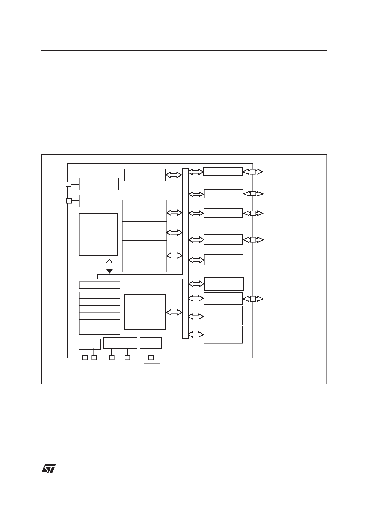
Figure 1. Block Diagram
TEST
NMI INTERRUPT
PROGRAM
PC
STACK LEVEL 1
STACK LEVEL 2
STACK LEVEL 3
STACK LEVEL 4
STACK LEVEL 5
STACK LEVEL 6
POWER
SUPPLY
OSCILLATOR
RESET
DATA ROM
USER
SELECTABLE
DATA RAM
PORT A
PORT B
TIMER
DIGITAL
8 BIT CORE
TEST/V
PP
8-BIT
A/D CONVERTER
PA0..PA1 / 20 mA Sink
V
DDVSS
OSCin OSCout RESET
WATCHDOG
Memory
PORT C
SPI (SERIAL
PERIPHERAL
INTERFACE)
AUTORELOAD
TIMER
192 Bytes
7948
bytes
DATA EEPROM
128 Bytes
PA2/OVF/ 20mA Sink
PA3/PWM/20 mA Sink
PA4/Ain/CP1
PA5/Ain/CP2
PB4..PB6/Ain
PC4..PC7/Ain
PORT D
PD6,PD7/Ain
PD1/Ain/Scl
PD2/Ain/Sin
PD3/Ain/Sout
PD4/Ain/RXD1
PD5/Ain/TXD1
(V
PP
on EPROM/OTP versions only)
TIMER
VR01823F
UART
21
Page 6

6/86
ST62T30B ST62E30B
INTRODUCTION (Cont’d)
OTP and EPROM devices are functionally identical. TheROM based versions offer the same functionality selecting as ROM options the options defined in the programmable option byte of the
OTP/EPROM versions.OTP devices offer all the
advantages of user programmability at low cost,
which make them the ideal choice in a wide range
of applications where frequent code changes, multiple code versions or last minute programmability
are required.
Figure 2. ST62T30B/E30B Pin Configuration
These compact low-cost devices feature a Timer
comprising an 8-bit counter and a 7-bit programmable prescaler, an 16-bit Auto-Reload Timer,
with 2 input capture channels, EEPROM data capability, a serial synchronous port communication
interface (SPI), a serial asynchronous port interface (UART), an 8-bit A/D Converter with 16 analog inputs and a Digital Watchdog timer, making
them well suited for a wide range of automotive,
appliance and industrial applications.
1
2
3
4
5
6
7
8
9
10
11
12
13
14
15
16
17
18
19
20
V
DD
TIMER
OSCin
OSCout
NMI
TEST/V
PP
(1)
RESET
Ain/PC7
Ain/PC6
Ain/PC5
V
SS
PA0
PA1
PA2/OVF
PA3/PWM
PD3/Ain/Sout
PD4/Ain/RXD1
PD5/Ain/TXD1
PD6/Ain
PD7/Ain
28
27
26
25
24
23
22
21
Ain/PC4
Ain/PB6
Ain/PB5
Ain/PB4
PA4/Ain/CP1
PA5/Ain/CP2
PD1/Ain/Scl
PD2/Ain/Sin
(1)
V
PP
on EPROM/OTP only
VR01804B
22
Page 7

7/86
ST62T30B ST62E30B
1.2 PIN DESCRIPTIONS
VDDand V
SS
. Power is supplied to the MCU via
these two pins. VDDis the power connection and
VSSis the ground connection.
OSCin and OSCout. These pins are internally
connected to the on-chip oscillator circuit. A quartz
crystal, a ceramic resonator or an external clock
signal can be connected between these two pins.
The OSCin pin is the input pin, the OSCout pin is
the output pin.
RESET
. The active-low RESET pin is used to re-
start the microcontroller.
TEST/VPP. The TEST must be held at VSSfor nor-
mal operation. If TEST pin is connected to a
+12.5V level during the reset phase, the
EPROM/OTP programming Mode is entered.
NMI.
The NMI pin provides the capability for asynchronous interruption, by applying an external non
maskable interrupt to the MCU.The NMI input is
falling edge sensitive with Schmitt trigger characteristics. The user can select as option the availability of an on-chip pull-up at this pin.
PA0-PA5. These 6 lines are organised as one I/O
port (A). Each line may be configured under software control as inputs with or without internal pullup resistors, interrupt generating inputs with pullup resistors, open-drain or push-pull outputs.
PA2/OVF, PA3/PWM, PA4/CP1 and PA5/CP2 can
be used respectively as overflow outputpin, output
compare pin, and astwo input capture pins for the
embedded 16-bit Auto-Reload Timer.
In addition, PA4-PA5 can also be used as analog
inputs for the A/D converter while PA0-PA3 can
sink 20mA for direct LED or TRIAC drive.
PB4-PB6.
These 3 lines are organised as one I/O
port (B). Each line may be configured under software control as inputs with or without internal pullup resistors, interrupt generating inputs with pullup resistors, open-drain or push-pull outputs, analog inputs for the A/D converter.
PC4-PC7
. These 4 lines are organised as one I/O
port (C). Each line may be configured under software control as input with or without internal pullup resistor, interrupt generating input with pull-up
resistor, analog input for the A/D converter, opendrain or push-pull output.
PD1-PD7. These 7 lines are organised as one I/O
port (portD). Each line may be configured under
software control as input with or without internal
pull-up resistor, interrupt generating input with
pull-up resistor, analog input open-drain or pushpull output. In addition, the pins PD5/TXD1 and
PD4/RXD1 can be used as UART output
(PD5/TXD1) or UARTinput (PD4/RXD1). The pins
PD3/Sout, PD2/Sin and PD1/SCL can also be
used respectively as data out, data in and Clock
pins for the on-chip SPI.
TIMER. This isthe TIMER 1I/O pin. Ininput mode,
it is connected to the prescaler and acts as external timer clock or as control gate for the internal
timer clock. In output mode, theTIMER pinoutputs
the data bit when a time-out occurs.The user can
select as option the availability of an on-chip pullup at this pin.
23
Page 8
8/86
ST62T30B ST62E30B
1.3 MEMORY MAP
1.3.1 Introduction
The MCU operates in three separate memory
spaces: Program space, Data space, and Stack
space. Operation in these three memory spaces is
described in the following paragraphs.
Briefly, Program space contains user program
code in Program memory and user vectors; Data
space contains user data in RAM and in Program
memory, and Stack space accommodates six levels of stack for subroutine and interrupt service
routine nesting.
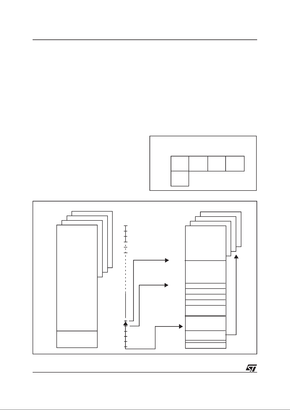
1.3.2 Program Space
Program Space comprises the instructions to be
executed, the data required for immediate addressing mode instructions, the reserved factory
test area and the user vectors. Program Space is
addressed via the 12-bit Program Counter register
(PC register).
Program Space is organised in four 2K pages.
Three of them are addressed in the 000h-7FFh locations of the Program Space by the Program
Counter and by writing the appropriate code in the
Program ROM Page Register (PRPR register). A
common (STATIC) 2K page is available all the
time for interrupt vectors and common subroutines, independently of the PRPR register content.
This “STATIC” page is directly addressed in the
0800h-0FFFh by the MSB of the Program Counter
register PC 11. Note this page can also be addressed in the 000-7FFh range. It is two different
ways of addressing the same physical memory.
Jump from a dynamic page to another dynamic
page is achieved by jumping back to the static
page, changing contents of PRPR and then jumping to the new dynamic page.
Figure 3. 8Kbytes Program Space Addressing
Figure 4. Memory Addressing Diagram
PC
SPACE
000h
7FFh
800h
FFFh
0000h
1FFFh
Page 0
Page 1
Static
Page
Page 2 Page 3
Page 1
Static
Page
ROM SPACE
PROGRAM SPACE
PROGRAM
INTERRUPT &
RESET VECTORS
ACCUMULATOR
DATA RAM
BANK SELECT
WINDOW SELECT
RAM
X REGISTER
Y REGISTER
V REGISTER
W REGISTER
DATA READ-ONLY
WINDOW
RAM / EEPROM
BANKING AREA
000h
03Fh
040h
07Fh
080h
081h
082h
083h
084h
0C0h
0FFh
0-63
DATA SPACE
0000h
0FF0h
0FFFh
MEMORY
MEMORY
DATA READ-ONLY
MEMORY
VR01568
24
Page 9
9/86
ST62T30B ST62E30B
MEMORY MAP (Cont’d)
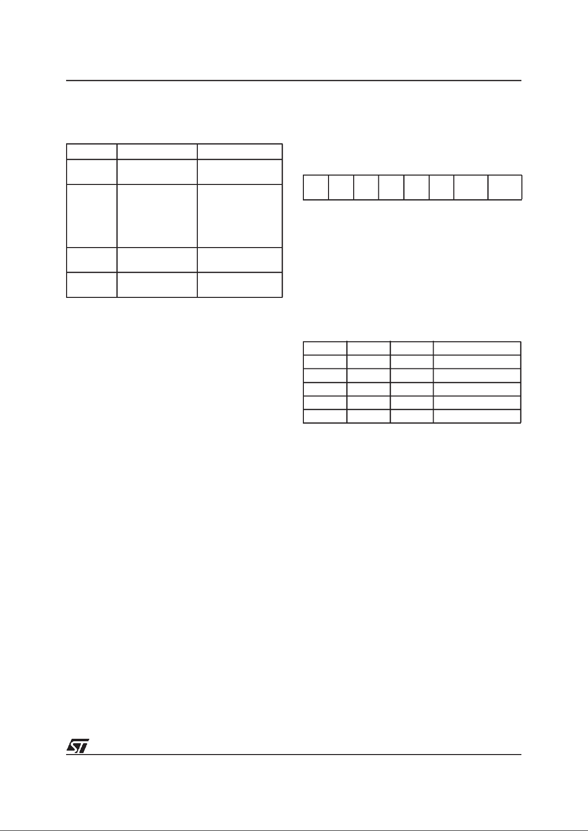
Table 1. ST62E30B/T30B Program Memory Map
Note: OTP/EPROM devices can be programmed
withthe development toolsavailablefrom STMicroelectronics (ST62E3X-EPB or ST623X-KIT).
1.3.2.1 Program ROM Page Register (PRPR)
The PRPR register can be addressed like a RAM
location in the Data Space at the address CAh;
nevertheless it is a write only register that cannot
be accessed with single-bit operations. This register is used to select the 2-Kbyte ROM bank of the
Program Space that will be addressed. The
number of the page has to be loaded in the PRPR
register. Refer to the Program Space description
for additional information concerning the use of
this register. The PRPR register is not modified
when an interrupt or a subroutine occurs.
Care is required when handling the PRPR register
as it is write only. For this reason, it is not allowed
to change the PRPR contents while executing interrupt service routine, as the service routine
cannot save and then restore its previous content.
This operation may be necessary if common routines and interrupt service routines take more than
2K bytes; in this case it could be necessary to divide the interrupt service routine into a (minor) part
in the static page (start and end) and to a second
(major) part in one of the dynamic pages. If it is impossible to avoid thewriting of this register in interrupt service routines, an image of this register
must be saved in a RAM location, and each time
the program writes to the PRPR it must write also
to the image register. The image register must be
written before PRPR, so if an interrupt occurs between the two instructions the PRPR is not affected.
Program ROM Page Register (PRPR)
Address: CAh — Write Only
Bits 2-7= Not used.
Bit 5-0 = PRPR1-PRPR0:
Program ROM Select.
These two bits select the corresponding page to
be addressed in the lower part of the 4K program
address space as specified inTable 2.
This register is undefined on Reset. Neither read
nor single bit instructions may be used to address
this register.
Table 2.8Kbytes Program ROM Page Register
Coding
1.3.2.2 Program Memory Protection
The Program Memory in OTP or EPROM devices
can be protected against external readout of memory by selecting the READOUT PROTECTION option in the option byte.
In the EPROM parts, READOUT PROTECTION
option can be disactivated only by U.V. erasure
that also results into the whole EPROM context
erasure.
Note: Once the Readout Protection is activated, it
is no longer possible, even for STMicroelectronics,
to gain access to the Program memory contents.
Returned parts with a protection set can therefore
not be accepted.
ROM Page Device Address Description
Page 0
0000h-007Fh
0080h-07FFh
Reserved
User ROM
Page 1
“STATIC”
0800h-0F9Fh
0FA0h-0FEFh
0FF0h-0FF7h
0FF8h-0FFBh
0FFCh-0FFDh
0FFEh-0FFFh
User ROM
Reserved
Interrupt Vectors
Reserved
NMI Vector
Reset Vector
Page 2
0000h-000Fh
0010h-07FFh
Reserved
User ROM
Page 3
0000h-000Fh
0010h-07FFh
Reserved
User ROM
70
- - - - - - PRPR0 PRPR1
PRPR1 PRPR0 PC bit 11 Memory Page
X X 1 Static Page (Page 1)
0 0 0 Page 0
0 1 0 Page 1 (Static Page
1 0 0 Page 2
1 1 0 Page 3
25
Page 10

10/86
ST62T30B ST62E30B
MEMORY MAP (Cont’d)
1.3.3 Data Space
Data Space accommodates all the data necessary
for processing the user program. This space comprises the RAM resource, the processor core and
peripheral registers, as well as read-only data
such as constants and look-up tables in Program
memory.
1.3.3.1 Data ROM
All read-only data is physically stored in program
memory, which also accommodates the Program
Space. The program memory consequently contains the program code to be executed, as well as
the constants and look-up tables required by the
application.
The Data Space locations in which the different
constants and look-up tables are addressed by the
processor core may be thought of as a 64-byte
window through which it is possible to access the
read-only data stored in Program memory.
1.3.3.2 Data RAM/EEPROM
In ST6230B and ST62E30B devices, the data
space includes 60 bytes of RAM, the accumulator
(A), the indirect registers (X), (Y), the short direct
registers (V), (W), the I/O port registers, the peripheral data and control registers, the interrupt
option register and the Data ROM Window register
(DRW register).
Additional RAM and EEPROM pages can also be
addressed using banks of 64 bytes located between addresses 00h and 3Fh.
1.3.4 Stack Space
Stack space consists of six 12-bit registers which
are used to stack subroutine and interrupt return
addresses, as well as the current program counter
contents.
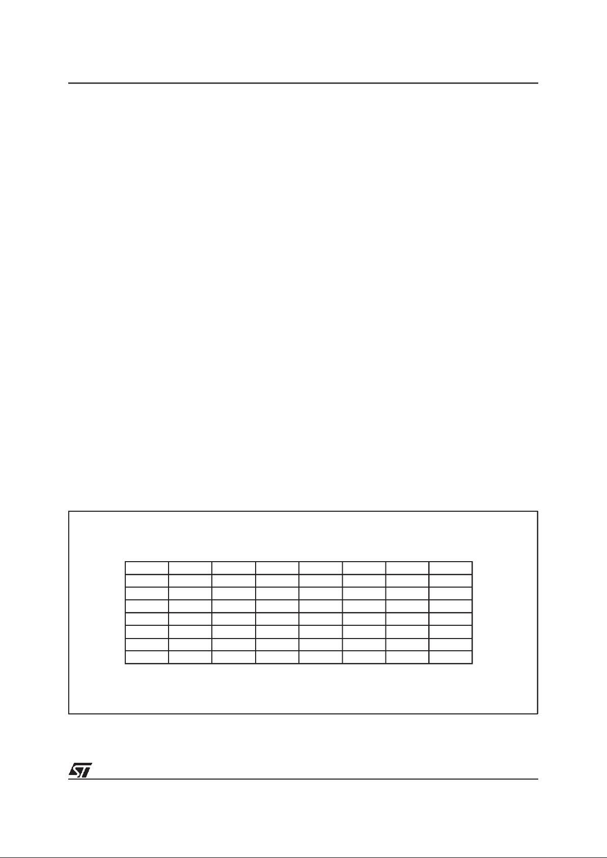
Table 3. Additional RAM/EEPROM Banks.
Table 4. ST62T30B/E30B Data Memory Space
Device RAM EEPROM
ST62T30B/E30B 2 x 64 bytes 2 x 64 bytes
DATAand EEPROM
000h
03Fh
DATA ROM WINDOW AREA
040h
07Fh
X REGISTER 080h
Y REGISTER 081h
V REGISTER 082h
W REGISTER 083h
DATARAM
084h
0BFh
PORT A DATA REGISTER 0C0h
PORT B DATA REGISTER 0C1h
PORT C DATA REGISTER 0C2h
PORT D DATA REGISTER 0C3h
PORT A DIRECTION REGISTER 0C4h
PORT B DIRECTION REGISTER 0C5h
PORT C DIRECTION REGISTER 0C6h
PORT D DIRECTION REGISTER 0C7h
INTERRUPT OPTION REGISTER 0C8h*
DATA ROM WINDOWREGISTER 0C9h*
ROM BANK SELECT REGISTER 0CAh*
RAM/EEPROMBANK SELECTREGISTER 0CBh*
PORT A OPTION REGISTER 0CCh
PORT B OPTION REGISTER 0CDh
PORT C OPTION REGISTER 0CEh
PORT D OPTION REGISTER 0CFh
A/D DATA REGISTER 0D0h
A/D CONTROL REGISTER 0D1h
TIMER 1 PRESCALER REGISTER 0D2h
TIMER 1 COUNTER REGISTER 0D3h
TIMER 1 STATUS/CONTROLREGISTER 0D4h
RESERVED 0D5h
UART DATASHIFT REGISTER 0D6h
UARTSTATUS CONTROL REGISTER 0D7h
WATCHDOG REGISTER 0D8h
RESERVED 0D9h
I/O INTERRUPT POLARITY REGISTER 0DAh
OSCILLATOR CONTROL REGISTER 0DBh
SPI INTERRUPT DISABLEREGISTER 0DCh*
SPI DATA REGISTER 0DDh
RESERVED 0DEh
EEPROM CONTROL REGISTER 0DFh
ARTIM16 COMPAREMASK REG. LOW BYTE MASK 0E0h
ARTIM16 2ND STATUSCONTROL REGISTERSCR2 0E1h
ARTIM16 3RD STATUSCONTROL REGISTERSCR3 0E2h
ARTIM16 4TH STATUSCONTROL REGISTER SCR4 0E3h
ARTIM16 1ST STATUSCONTROL REGISTER SCR1 0E8h
ARTIM16 RELOAD CAPTURE REG. HIGH BYTE RLCP 0E9h
ARTIM16 RELOAD CAPTURE REG. LOW BYTE RLCP 0EAh
ARTIM16 CAPTURE REGISTER HIGH BYTECP 0EBh
ARTIM16 CAPTURE REGISTER LOW BYTE CP 0ECh
ARTIM16COMPAREVALUE REGISTERHIGHBYTECMP 0EDh
ARTIM16COMPAREVALUEREGISTERLOWBYTECMP 0EEh
ARTIM 16 COMPARE MASK REG. HIGH BYTE MASK 0EFh
RESERVED
0F0h
0FBh
RESERVED
OFCh
0FDh
0FEh
ACCUMULATOR OFFh
* WRITE ONLY REGISTER
26
Page 11
11/86
ST62T30B ST62E30B
MEMORY MAP (Cont’d)
1.3.5 Data Window Register (DWR)
The Dataread-only memory window is locatedfrom
address 0040h to address 007Fh in Data space. It
allows direct reading of 64 consecutive bytes located anywhere in program memory, between address 0000h and 1FFFh (top memory address depends on the specific device). All the program
memory can therefore be used to store either instructions or read-only data. Indeed, the window
can be moved in steps of 64 bytes along the programmemory by writingtheappropriate codeinthe
Data Window Register (DWR).
The DWRcan be addressed like any RAM location
in the Data Space, it is however a write-only register and therefore cannot be accessed using singlebit operations. This register is used to position the
64-byte read-only data window (from address 40h
to address 7Fh of the Data space) in program
memory in 64-byte steps. The effective address of
the byte to be read as data in program memory is
obtained by concatenating the 6 least significant
bits of the register address given in the instruction
(as least significant bits) and the content of the
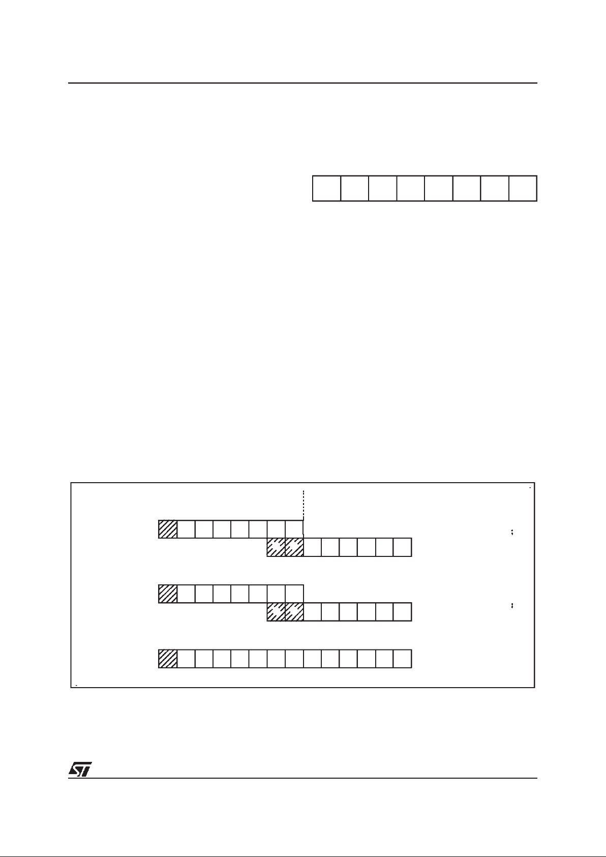
DWR register (as most significantbits), as illustrated inFigure 5below. For instance, when addressing location 0040h of the Data Space, with 0 loaded in the DWR register, the physical location addressed in program memory is 00h. The DWR register is not cleared on reset, therefore it must be
written to prior tothe first access to the Data readonly memory window area.
Data Window Register (DWR)
Address: 0C9h — Write Only
Bits 7 = Not used.
Bit 6-0 =
DWR5-DWR0:
Data read-only memory
Window Register Bits.
These are the Data readonly memory Window bits that correspond to the
upper bits of the data read-only memory space.
Caution:
This register is undefined on reset. Neither read nor single bit instructions may beused to
address this register.
Note:
Care is required when handling the DWR
register as it is write only. For this reason, the
DWR contents should not be changed while executing an interrupt service routine, as the service
routine cannot save and then restore the register’s
previous contents. If it is impossible to avoid writing to theDWR during the interrupt service routine,
an image of the register must be saved in a RAM
location, and each time the program writes to the
DWR, it must also write to the image register. The
image register must be written first so that, if an interrupt occurs between the two instructions, the
DWR is not affected.
Figure 5. Data read-only memory Window Memory Addressing
70
- DWR6 DWR5 DWR4 DWR3 DWR2 DWR1 DWR0
DATA ROM
WINDOW REGISTER
CONTENTS
DATA SPACE ADDRESS
40h-7Fh
IN INSTRUCTION
PROGRAM SPACE ADDRESS
765432 0
543210
543210
READ
1
67891011
0
1
VR0A1573
12
1
0
DATA SPACE ADDRESS
59h
0000
0
1
00
1
11
Example:
(DWR)
DWR=28h
11000000001
ROM
ADDRESS:A19h
11
13
01
27
Page 12

12/86
ST62T30B ST62E30B
MEMORY MAP (Cont’d)
1.3.6 Data RAM/EEPROM Bank Register
(DRBR)
Address: CBh — Write only
Bit 7-5 = These bits are not used
Bit 4 - DRBR4. This bit, when set, selects RAM
Page 2.
Bit 3 - DRBR3. This bit, when set, selects RAM
Page 1.
Bit2. This bit is not used.
Bit 1 - DRBR1. This bit, when set, selects
EEPROM Page 1.
Bit 0 - DRBR0. This bit, when set, selects
EEPROM Page 0.
The selection of the bank ismade byprogramming
the Data RAM Bank Switch register (DRBR register) located at address CBh of the Data Space according to Table 1. No more than one bank should
be set at a time.
The DRBR register can be addressed like a RAM
Data Space at the address CBh; nevertheless it is
a write only register that cannot be accessed with
single-bit operations. This register is used to select
the desired 64-byte RAM/EEPROM bank of the
Data Space. The number of banks has to be loaded in the DRBR register and the instruction has to
point to the selected location as if it was in bank 0
(from 00h address to 3Fh address).
This register is not cleared during the MCU initialization, therefore it must be written before the first
access to the Data Space bank region. Refer to
the Data Space description for additional information. The DRBR register is not modified when an
interrupt or a subroutine occurs.
Notes:
Care isrequired when handling the DRBR register
as it is write only. For this reason, it is not allowed
to change the DRBR contents while executing interrupt service routine, as the service routine cannot save and then restore its previous content. If it
is impossible to avoid the writing of this register in
interrupt service routine, an image of this register
must be saved in a RAM location, and each time
the program writes to DRBR it must write also to
the image register. The image register must be
written first, so if an interrupt occurs between the
two instructions the DRBR is not affected.
In DRBR Register, only 1 bit must be set. Otherwise two or more pages are enabled in parallel,
producing errors.
Table 5. Data RAM Bank Register Set-up
70
- - - DRBR4 DRBR3 - DRBR1 DRBR0
DRBR ST62T30B/E30B
00 None
01 EEPROM Page 0
02 EEPROM Page 1
08 RAM Page 1
10h RAM Page2
other Reserved
28
Page 13
13/86
ST62T30B ST62E30B
MEMORY MAP (Cont’d)
1.3.7 EEPROM Description
EEPROM memory is located in 64-byte pages in
data space. This memory may be used by the user
program for non-volatile data storage.
Data space from 00h to 3Fh is paged as described
in Table 6. EEPROM locations are accessed directly by addressing these paged sections of data
space.
The EEPROM does not require dedicated instructions for read orwriteaccess.Once selected via the
Data RAM Bank Register, the active EEPROM
page is controlled bythe EEPROM Control Register (EECTL), which is described below.
BitE20FF oftheEECTLregister mustbereset prior
to any write or read access to the EEPROM. If no
bank hasbeenselected, orifE2OFF is set,any access is meaningless.
Programming must be enabled by setting the
E2ENA bit of the EECTL register.
The E2BUSYbit of the EECTL register is setwhen
the EEPROM is performing a programming cycle.
Any access to the EEPROM when E2BUSY is set
is meaningless.
Provided E2OFF and E2BUSY are reset, an EEPROM location is read just like any other data location, also in terms of access time.
Writing to the EEPROM may be carried out in two
modes: Byte Mode (BMODE) and Parallel Mode
(PMODE). In BMODE, one byte is accessed at a
time, while in PMODE up to 8 bytes in the same
row are programmed simultaneously (with consequent speed and power consumption advantages,
the latter being particularly important in battery
powered circuits).
General Notes:
Data should be written directly to the intended ad-
dress in EEPROM space. There is no buffer memory between data RAM and the EEPROM space.
When the EEPROM is busy (E2BUSY = “1”)
EECTL cannot be accessed in write mode, it is
only possible to read the status of E2BUSY. This
implies that as long as the EEPROM is busy, it is
not possible to change the status of the EEPROM
Control Register. EECTL bits 4 and 5 are reserved
and must never be set.
Care is requiredwhen dealing with the EECTL register, as some bits are write only. For this reason,
the EECTL contents must not be altered while executing an interrupt service routine.
If it is impossible to avoid writing to this register
within an interrupt service routine, an image of the
register must be saved in a RAM location, and
each time the program writes to EECTL it must
also writeto the image register. The image register
must be written to first so that, if an interrupt occurs between the two instructions, the EECTL will
not be affected.
Table 6. Row Arrangement for Parallel Writing of EEPROM Locations
Dataspace
addresses.
Banks 0 and 1.
Byte 01234567
ROW7 38h-3Fh
ROW6 30h-37h
ROW5 28h-2Fh
ROW4 20h-27h
ROW3 18h-1Fh
ROW2 10h-17h
ROW1 08h-0Fh
ROW0 00h-07h
Up to 8 bytes in each row may be programmed simultaneously in Parallel Write mode.
The number of available 64-byte banks (1 or 2) is device dependent.
29
Page 14

14/86
ST62T30B ST62E30B
MEMORY MAP (Cont’d)
Additional Notes on Parallel Mode:
If the user wishes to perform parallel programming, the first step should be to set the E2PAR2
bit. From this time on, the EEPROM will be addressed in write mode, the ROW address will be
latched and it will be possible to change it only at
the end of the programming cycle, or by resetting
E2PAR2 without programming the EEPROM. After the ROW address is latched, the MCU can only
“see” the selected EEPROM row and any attempt
to write or read other rows will produce errors.
The EEPROM should not be read while E2PAR2
is set.
As soon as the E2PAR2 bit is set, the 8 volatile
ROW latches are cleared. From this moment on,
the user can load data in all or in part of the ROW.
Setting E2PAR1 will modify the EEPROM registers corresponding to the ROW latches accessed
after E2PAR2. For example, if the software sets
E2PAR2 and accesses the EEPROM by writing to
addresses 18h, 1Ah and 1Bh, and then sets
E2PAR1, these three registers will be modified simultaneously; the remaining bytes in the row will
be unaffected.
Note that E2PAR2 is internally reset at the end of
the programming cycle. This implies that the user
must set the E2PAR2 bit between two parallel programming cycles. Note that if the user tries to set
E2PAR1 while E2PAR2 is not set, there will be no
programming cycle and theE2PAR1 bit will be unaffected. Consequently, the E2PAR1 bit cannot be
set if E2ENA is low. The E2PAR1 bit can be set by
the user, only if the E2ENA and E2PAR2 bits are
also set.
EEPROM Control Register (EECTL)
Address: DFh — Read/Write
Reset status: 00h
Bit 7 =D7:
Unused.
Bit6=E2OFF:
Stand-by Enable Bit.
WRITE ONLY.
Ifthisbitis settheEEPROMisdisabled(any access
willbemeaningless) andthepowerconsumption of
the EEPROM is reduced to its lowest value.
Bit 5-4 =D5-D4:
Reserved.
MUST be kept reset.
Bit 3 =
E2PAR1
:
Parallel Start Bit.
WRITE ONLY.
OnceinParallelMode,assoonastheusersoftware
sets the E2PAR1 bit, parallel writing of the 8 adjacent registers will start. This bitisinternally reset at
the end of the programming procedure. Note that
less than 8 bytes can bewritten ifrequired, the undefined bytes being unaffected by the parallel programming cycle; this is explained in greater detail in
the Additional Notes on Parallel Mode overleaf.
Bit 2 = E2PAR2:
Parallel Mode En. Bit.
WRITE
ONLY. This bit must be setby the user program in
order to perform parallel programming. If E2PAR2
is set and the parallel start bit (E2PAR1) is reset,
up to 8 adjacent bytes can be written simultaneously. These 8 adjacent bytes are considered as a
row, whose address lines A7, A6, A5, A4, A3 are
fixed while A2, A1andA0 arethe changing bits, as
illustrated in Table 6. E2PAR2 is automatically reset at the end of any parallel programming procedure. It can be reset by the user software before
starting the programming procedure, thus leaving
the EEPROM registers unchanged.
Bit 1 = E2BUSY:
EEPROM Busy Bit.
READ ONLY. This bit is automatically set by the EEPROM
control logic when the EEPROM is in programming mode. The user program should test it before
any EEPROM read or write operation; any attempt
to access the EEPROM while the busy bit is set
will be aborted and the writing procedure in
progress will be completed.
Bit 0 = E2ENA:
EEPROM Enable Bit.
WRITE ONLY. This bit enables programming of the EEPROM
cells. It must be set before any write to the EEPROM register. Any attempt to write to the EEPROM when E2ENA is low is meaningless and will
not trigger a write cycle.
70
D7 E2OFF D5 D4 E2PAR1 E2PAR2 E2BUSY E2ENA
30
Page 15

15/86
ST62T30B ST62E30B
1.4 PROGRAMMING MODES
1.4.1 Option Byte
The Option Byte allows configuration capability to
the MCUs. Option byte’s content is automatically
read, and the selected options enabled, when the
chip reset is activated.
It can only be accessed during the programming
mode. This access is made either automatically
(copy from a master device) or by selecting the
OPTION BYTE PROGRAMMING mode ofthe programmer.
The option byte is located in a non-user map. No
address has to be specified.
EPROM Code Option Byte
Bit 7. Reserved.
Bit 6 =
PORT PULL
. This bit must be set high to
have pull-up input state at reset on the I/O port.
When this bit is low, I/O ports are in input without
pull-up (high impedance) state at reset
Bit 5 =
EXTCNTL
. This bit selects the External
STOP Mode capability. When EXTCNTL is high,
pin NMI controls if the STOP mode can be accessed when the watchdog is active. When EXTCNTL is low, the STOP instruction is processed as a
WAIT as soon as the watchdog is active.
Bit 4 = PROTECT. This bit allows the protection of
the software contents against piracy. When the bit
PROTECT is set high, readout of the OTP contents is prevented by hardware. No programming
equipment is able to gain access to the user program. When this bit is low, the user program can
be read.
Bit 3 =TIM PULL.This bit must be set high toconfigure the TIMER pin with a pull up resistor. When
it is low, no pull up is provided.
Bit 2 =NMI PULL. This bit mustbe set high toconfigure the NMI pin with a pull up resistor when it is
low, no pull up is provided.
Bit 1 = WDACT. This bit controls the watchdog activation. When it is high, hardware activation is selected. The software activation is selected when
WDACT is low.
Bit 0 =OSGEN.This bit must be set high to enable
the oscillator Safe Guard. When this bit is low, the
OSG is disabled.
The Option byte is written during programming either by using the PC menu (PC driven Mode) or
automatically (stand-alone mode)
1.4.2 Program Memory
EPROM/OTP programming mode is set by a
+12.5V voltage applied to the TEST/VPPpin. The
programming flow of the ST62T30B/E30B is described in the User Manual of the EPROM Programming Board.
The MCUs can be programmed with the
ST62E3xB EPROM programming tools available
from STMicroelectronics.
1.4.3 EEPROM Data Memory
EEPROM data pages are supplied in the virgin
state FFh. Partial or total programming of EEPROM data memory can be performed either
through the application software, or through an external programmer. Any STMicroelectronics tool
used for the program memory (OTP/EPROM) can
also be used to program the EEPROM data memory.
1.4.4 EPROM Erasing
The EPROM of the windowed package of the
MCUs may be erased by exposure to Ultra Violet
light. The erasure characteristic of the MCUs is
such that erasure begins when the memory is exposed to light with a wave lengths shorter than approximately 4000Å. It should be noted that sunlights and some types of fluorescent lamps have
wavelengths in the range 3000-4000Å.
It is thus recommended that the window of the
MCUs packages becovered by an opaque label to
prevent unintentional erasure problems when testing the application in such an environment.
The recommended erasure procedure of the
MCUs EPROM is the exposure to short wave ultraviolet light which have a wave-length 2537A.
The integrated dose (i.e. U.V. intensity x exposure
time) for erasure should be a minimum of 15Wsec/cm2. The erasure time with this dosage is approximately 15 to 20 minutes using an ultraviolet
lamp with 12000µW/cm2power rating. The
ST62E30B should be placed within 2.5cm (1Inch)
of the lamp tubes during erasure.
70
-
PORT
PULL
EXTCNTLPROTECT
TIM
PULL
NMI
PULL
WDACT OSGEN
31
Page 16
16/86
ST62T30B ST62E30B
2 CENTRAL PROCESSING UNIT
2.1 INTRODUCTION
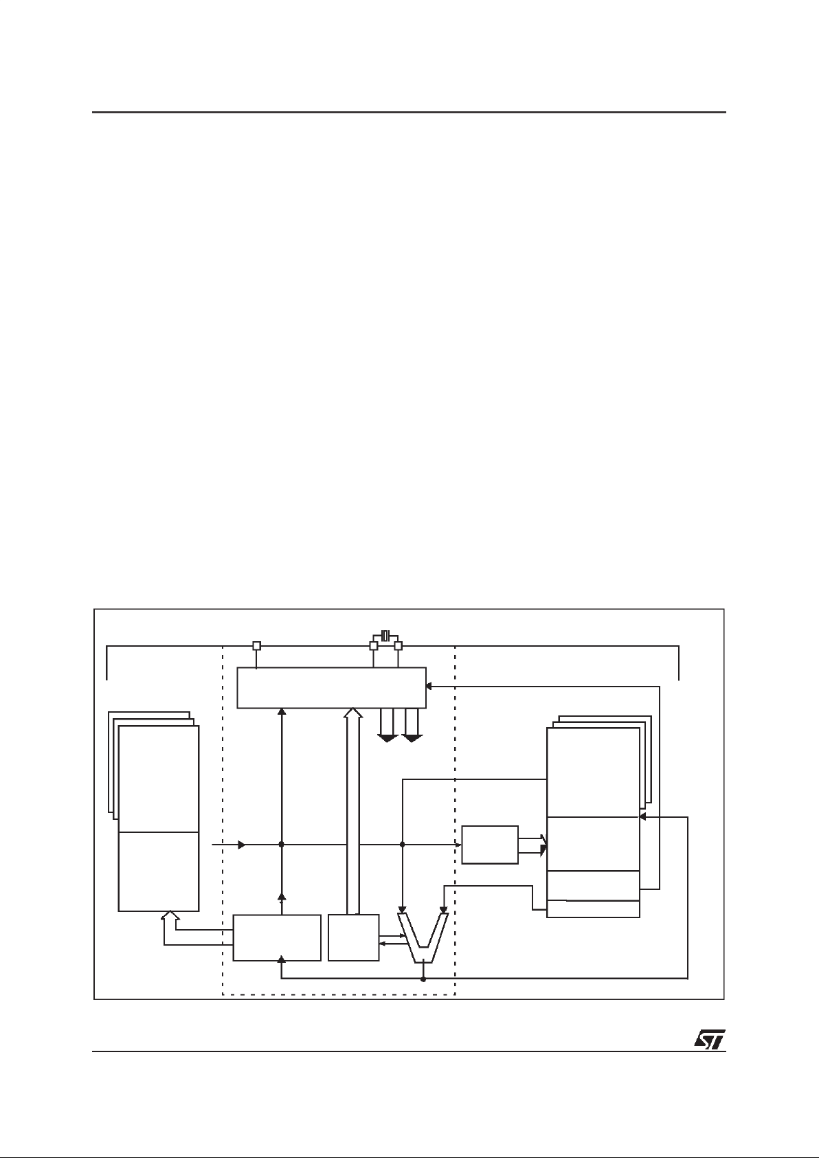
The CPUCoreofST6devicesisindependent ofthe
I/O or Memory configuration. As such, it may be
thought of as an independent central processor
communicating with on-chip I/O, Memory and Peripherals via internal address, data, and control
buses. In-core communication is arranged as
shown in Figure 6; the controller being externally
linked to both the Reset and Oscillator circuits,
while the core islinked to the dedicated on-chip peripherals via the serial data bus and indirectly, for
interrupt purposes, through the control registers.
2.2 CPU REGISTERS
TheST6FamilyCPUcorefeaturessixregistersand
three pairs of flags available to the programmer.
These are described in the following paragraphs.
Accumulator (A). The accumulator is an 8-bit
general purpose register used in all arithmetic calculations, logical operations, and data manipulations. The accumulator can be addressed in Data
space asa RAM location ataddress FFh. Thus the
ST6 can manipulate the accumulator just like any
other register in Data space.
Indirect Registers (X, Y).These two indirect registers are used as pointers to memory locations in
Data space. They are used in the register-indirect
addressing mode. These registers can be addressed in the data space as RAM locations at addresses 80h (X) and 81h (Y). They can also be accessed with the direct, shortdirect, or bit direct addressing modes. Accordingly, the ST6 instruction
set can use the indirect registers as any other register of the data space.
Short Direct Registers (V, W).These two registers are used to save a byte in short direct addressing mode. They can be addressed in Data
space as RAM locations at addresses 82h (V) and
83h (W). They can also be accessed using the direct and bit direct addressing modes. Thus, the
ST6 instruction set can use the short direct registers as any other register of the data space.
Program Counter (PC). The program counter is a
12-bit register which contains the address of the
next ROM location to be processed by the core.
This ROM location may be an opcode, an operand, or the address of an operand. The 12-bit
length allows the direct addressing of 4096 bytes
in Program space.
Figure 6. ST6 Core Block Diagram
PROGRAM
RESET
OPCODE
FLAG
VALUES
2
CONTROLLER
FLAGS
ALU
A-DATA
B-DATA
ADDRESS/READ LINE
DATA SPACE
INTERRUPTS
DATA
RAM/EEPROM
DATA
ROM/EPROM
RESULTS TO DATA SPACE (WRITE LINE)
ROM/EPROM
DEDICATIONS
ACCUMULATOR
CONTROL
SIGNALS
OSCin
OSCout
ADDRESS
DECODER
256
12
Program Counter
and
6 LAYER STACK
0,01 TO 8MHz
VR01811
32
Page 17
17/86
ST62T30B ST62E30B
CPU REGISTERS (Cont’d)
However, ifthe program space contains more than
4096 bytes, the additional memory in program
space can be addressed by using the Program
Bank Switch register.
The PC value is incremented after reading the address of the current instruction. To execute relative
jumps, the PC and the offset are shifted through
the ALU, where they are added; the result is then
shifted back into the PC. The program counter can
be changed in the following ways:
- JP (Jump) instructionPC=Jump address
- CALL instructionPC= Call address
- Relative Branch Instruction.PC= PC +/- offset
- Interrupt PC=Interrupt vector
- Reset PC= Reset vector
- RET & RETI instructionsPC= Pop (stack)
- Normal instructionPC= PC + 1
Flags (C, Z). The ST6 CPU includes three pairs of
flags (Carry and Zero), each pairbeing associated
with one of the three normal modes of operation:
Normal mode, Interrupt mode and Non Maskable
Interrupt mode. Each pair consists of a CARRY
flag and a ZERO flag. One pair (CN, ZN) is used
during Normal operation, another pair is used during Interrupt mode (CI, ZI), and a third pair is used
in the Non Maskable Interrupt mode (CNMI, ZNMI).
The ST6 CPU uses the pair of flags associated
with the current mode: as soon as an interrupt (or
a Non Maskable Interrupt) is generated, the ST6
CPU uses the Interrupt flags (resp. the NMI flags)
instead of the Normal flags. When the RETI instruction is executed, the previously used set of
flags is restored. It should be noted that each flag
set can only be addressed in its own context (Non
Maskable Interrupt, Normal Interrupt or Main routine). The flags are not cleared during context
switching and thus retain their status.
The Carry flag is set when a carry or a borrow occurs during arithmetic operations; otherwise it is
cleared. The Carry flag is also set to the value of
the bit tested in a bit test instruction; it also participates in the rotate left instruction.
The Zero flag is set if the result of the last arithmetic or logical operation was equal to zero; otherwise it is cleared.
Switching between the three sets of flags is performed automatically when an NMI, an interrupt or
a RETI instructions occurs. As the NMI mode is
automatically selected after the reset of the MCU,
the ST6 core uses at first the NMI flags.
Stack. The ST6 CPU includes a true LIFO hardware stack which eliminates the need for a stack
pointer. The stack consists of six separate 12-bit
RAM locations that do not belong to the data
space RAM area. When a subroutine call (or interrupt request) occurs, the contents of each level are
shifted into the next higher level, while the content
of the PC is shifted into the first level (the original
contents of the sixth stack level are lost). When a
subroutine or interrupt return occurs (RETor RETI
instructions), the first level register is shifted back
into the PC and the value of each level is popped
back into the previous level. Since the accumulator, in common with all other data space registers,
is not stored in this stack, management of these
registers should be performed within the subroutine. The stack will remain in its “deepest” position
if more than 6 nested calls or interrupts are executed, and consequently the last return address will
be lost. It will also remain in its highest position if
the stack is empty and a RET or RETI is executed.
In this case the next instruction will be executed.
Figure 7. ST6 CPU Programming Mode
l
SHORT
DIRECT
ADDRESSING
MODE
V REGISTER
WREGISTER
PROGRAM COUNTER
SIX LEVELS
STACK REGISTER
CZNORMAL FLAGS
INTERRUPT FLAGS
NMI FLAGS
INDEX
REGISTER
VA000423
b7
b7
b7
b7
b7
b0
b0
b0
b0
b0
b0b11
ACCUMULATOR
YREG.POINTER
XREG.POINTER
CZ
CZ
33
Page 18

18/86
ST62T30B ST62E30B
3 CLOCKS, RESET, INTERRUPTS AND POWER SAVING MODES
3.1 CLOCK SYSTEM
The MCU features a Main Oscillator which can be
driven by an external clock, or used in conjunction
with an AT-cut parallel resonant crystal or a suitable ceramic resonator. In addition, a Low Frequency Auxiliary Oscillator (LFAO) can be switched in
for security reasons, to reduce power consumption, or to offer the benefits of a back-up clock system.
The Oscillator Safeguard (OSG) option filters
spikes from the oscillator lines, provides access to
the LFAO to provide a backup oscillator in the
event of main oscillator failure and also automatically limits the internal clock frequency (f
INT
)asa
function ofVDD, in order to guarantee correct operation. These functions are illustrated inFigure 9,
Figure 10, Figure 11 and Figure 12.
Figure 8 illustrates various possible oscillator configurations using anexternal crystalorceramic resonator, anexternal clockinputorthelowestcostsolution using onlytheLFAO.CL1an CL2should have
acapacitance intherange12to22pFforanoscillator
frequency in the 4-8 MHz range.
The internal MCU clock frequency (f
INT
) is divided
by 12 to drive the Timer and the Watchdog timer,
and by 13 to drive the CPU core, while the A/D
converter is driven by f
INT
divided either by 6 or by
12 as may be seen inFigure 11.
With an 8MHz oscillator frequency, thefastest ma-
chine cycle is therefore 1.625µs.
A machine cycleis the smallest unit oftime needed
toexecute any operation (for instance, to increment
the Program Counter). An instruction may require
two, four, or five machine cycles for execution.
3.1.1 Main Oscillator
The main oscillator can be turned off (when the
OSG ENABLED option is selected) by setting the
OSCOFF bit of the OSCR Control Register. The
Low Frequency Auxiliary Oscillator is automatically started.
Figure 8. Oscillator Configurations
INTEGRATEDCLOCK
OSG ENABLED option
OSC
in
OSC
out
C
L1n
C
L2
ST6xxx
CRYSTAL/RESONATOR CLOCK
OSC
in
OSC
out
ST6xxx
EXTERNAL CLOCK
NC
OSC
in
OSC
out
ST6xxx
NC
VA0016
VA0015A
34
Page 19

19/86
ST62T30B ST62E30B
CLOCK SYSTEM (Cont’d)
Turning on the main oscillator is achieved by resetting the OSCOFF bit of the OSCR Register or
by resetting the MCU. Restarting the main oscillator implies a delay comprising the oscillator start
up delay period plus the duration of the software
instruction at f
LFAO
clock frequency.
3.1.2 Low Frequency Auxiliary Oscillator
(LFAO)
The Low Frequency Auxiliary Oscillator has three
main purposes. Firstly, it can be used to reduce
power consumption in non timing critical routines.
Secondly, it offers a fully integrated system clock,
without any external components. Lastly, it acts as
a safety oscillator in case of main oscillator failure.
This oscillator is available when the OSG ENABLED option is selected. In this case, it automatically starts one of its periods after the first missing
edge from the main oscillator, whatever the reason
(main oscillator defective, no clock circuitry provided, main oscillator switched off...).
User code, normal interrupts, WAIT and STOP instructions, are processed as normal, at the reduced f
LFAO
frequency. The A/D converter accuracy is decreased, since theinternal frequency isbelow 1MHz.
At power on, the Low Frequency Auxiliary Oscillator starts faster than the Main Oscillator. It therefore feeds the on-chip counter generating thePOR
delay until the Main Oscillator runs.
The Low Frequency Auxiliary Oscillator is automatically switched off as soon as the main oscillator starts.
OSCR
Address: 0DBh — Read/Write
Bit 7-1= These bits are not used and must be kept
cleared after reset.
Bit 0 =
OSCOFF
.
Main oscillator turn-off.
When
low, this bit enables main oscillator to run. The
main oscillator is switched off when OSCOFF is
high.
3.1.3 Oscillator Safe Guard
The Oscillator Safe Guard (OSG) affords drastically increased operational integrity in ST62xx devices. The OSG circuit provides three basic functions: it filters spikes from the oscillator lines which
would result in over frequency to the ST62 CPU; it
gives access to the Low Frequency Auxiliary Oscillator (LFAO), used to ensure minimum processing in case of main oscillator failure, to offer reduced power consumption or to provide a fixed frequency low cost oscillator; finally, it automatically
limits the internal clock frequency as a function of
supply voltage, in order to ensure correct operation even if the power supply should drop.
The OSG is enabled or disabled by choosing the
relevant OSG option. It may be viewed as a filter
whose cross-over frequency is device dependent.
Spikes on the oscillator linesresult in aneffectively
increased internal clock frequency. In the absence
of an OSG circuit, this may lead to an over frequency for a given power supply voltage. The
OSG filters out such spikes (asillustrated inFigure
9). In all cases, when the OSG is active, the maximum internal clock frequency, f
INT
, is limited to
f
OSG
, which is supply voltage dependent. This re-
lationship is illustrated inFigure 12.
When the OSG is enabled, the Low Frequency
Auxiliary Oscillator may be accessed. This oscillator starts operating after the first missing edge of
the main oscillator (seeFigure 10).
Over-frequency, at a given power supply level, is
seen by the OSG as spikes; it therefore filters out
some cycles in order that the internal clock frequency of the device is kept within the range the
particular device can stand (depending on VDD),
and below f
OSG
: the maximum authorised frequen-
cy with OSG enabled.
Note. The OSGshould beused whereverpossible
as it provides maximum safety. Care must be taken, however, as it can increase power consumption and reduce the maximum operating frequency
to f
OSG
.
70
-------
OSC
OFF
35
Page 20
20/86
ST62T30B ST62E30B
CLOCK SYSTEM (Cont’d)
Figure 9. OSG Filtering Principle
Figure 10. OSG Emergency Oscillator Principle
(1)
VR001932
(3)
(2)
(4)
(1)
(2)
(3)
(4)
Maximum Frequency for the device to work correctly
Actual Quartz Crystal Frequency at OSCin pin
Noise from OSCin
Resulting Internal Frequency
Main
VR001933
Internal
Emergency
Oscillator
Frequency
Oscillator
36
Page 21
21/86
ST62T30B ST62E30B
CLOCK SYSTEM (Cont’d)
Figure 11. Clock Circuit Block Diagram
Figure 12. Maximum Operating Frequency (f
MAX
) versus Supply Voltage (VDD)
Notes
:
1. In this area, operation is guaranteed at the quartz crystal frequency.
2. Whenthe OSG isdisabled, operation in this area is guaranteed atthe crystalfrequency. When the OSG
is enabled, operation in this area is guaranteed at a frequency of at least f
OSG Min.
3. When the OSG is disabled, operation in this area is guaranteed at the quartz crystal frequency. When
the OSG is enabled, access to this area is prevented. The internal frequency is kept a f
OSG.
4. When the OSG is disabled, operation in this area is not guaranteed
When the OSG is enabled, access to this area is prevented. The internal frequency is kept at f
OSG.
MAIN
OSCILLATOR
OSG
LFAO
M
U
X
Core
:13
:12
:1
TIMER 1
Watchdog
POR
f
INT
Main Oscillator off
ADC
ARTIMER 16
:6
M
U
X
1
2.5
3.5 4 4.5 5 5.5 6
8
7
6
5
4
3
2
Maximum FREQUENCY (MHz)
SUPPLY VOLTAGE (V
DD
)
FUNCTIONALITY IS NOT
3
4
3
2
1
f
OSG
f
OSG
Min
GUARANTEED
IN THIS AREA
VR01807
37
Page 22

22/86
ST62T30B ST62E30B
3.2 RESETS
The MCU can be reset in three ways:
– by the external Reset input being pulled low;
– by Power-on Reset;
– by the digital Watchdog peripheral timing out.
3.2.1 RESET Input
The RESET pin may be connected to a device of
the application board in order to reset the MCU if
required. The RESET pin may be pulled low in
RUN, WAIT or STOP mode. This input can be
used to reset the MCU internal state and ensure a
correct start-up procedure. The pin is active low
and features a Schmitt trigger input. The internal
Reset signal is generated by adding a delay to the
external signal. Therefore even short pulses on
the RESET pin are acceptable, provided VDDhas
completed its rising phase and that the oscillator is
running correctly (normal RUN or WAIT modes).
The MCU is kept in the Reset state as long as the
RESET pin is held low.
If RESET activation occurs in the RUN or WAIT
modes, processing of the user program is stopped
(RUN mode only), the Inputs and Outputs are configured as inputs with pull-up resistors and the
main Oscillator is restarted. When the level on the
RESET pin then goes high, the initialization sequence is executed following expiry of the internal
delay period.
If RESET pin activation occurs in the STOP mode,
the oscillator starts up and all Inputs and Outputs
are configured as inputs with pull-up resistors.
When the level of theRESET pin then goes high,
the initialization sequence is executed following
expiry of the internal delay period.
3.2.2 Power-on Reset
The function of the POR circuit consists in waking
up the MCU at an appropriate stage during the
power-on sequence. At the beginning of this sequence, the MCU is configured in the Reset state:
all I/O ports are configured as inputs with pull-up
resistors and no instruction is executed. When the
power supply voltage rises toa sufficient level, the
oscillator starts to operate, whereupon an internal
delay is initiated, in order to allow the oscillator to
fully stabilize before executing the first instruction.
The initialization sequence isexecuted immediately following the internal delay.
The internal delay isgenerated byanon-chip counter.The internal reset lineis released 2048 internal
clock cycles after release of the external reset.
Notes:
To ensure correct start-up, the user should take
care that the reset signal is notreleased before the
VDDlevel is sufficient to allow MCU operation at
the chosen frequency (see Recommended Operating Conditions).
A proper reset signal for a slow rising VDDsupply
can generally be provided by an external RC network connected to theRESET pin.
Figure 13.Reset and Interrupt Processing
INT LATCHCLEARED
NMI MASK SET
RESET
( IFPRESENT )
SELECT
NMI MODE FLAGS
IS RESET STILL
PRESENT?
YES
PUT FFEH
ON ADDRESSBUS
FROM RESET LOCATIONS
FFE/FFF
NO
FETCH INSTRUCTION
LOAD PC
VA000427
38
Page 23
23/86
ST62T30B ST62E30B
RESETS (Cont’d)
3.2.3 Watchdog Reset
The MCU provides a Watchdog timer function in
order to ensure graceful recovery from software
upsets. If the Watchdog register is not refreshed
before an end-of-count condition is reached, the
internal reset will be activated. This, amongst other things, resets the watchdog counter.
The MCU restarts just as though the Reset had
been generated by the RESET pin, including the
built-in stabilisation delay period.
3.2.4 Application Notes
No external resistor is required between VDDand
the Reset pin, thanks to the built-in pull-up device.
The POR circuit operates dynamically, in that it
triggers MCU initialization on detecting the rising
edge of VDD. The typical threshold is in the region
of 2 volts, but the actual value of the detected
threshold depends on the way in which VDDrises.
The POR circuit is
NOT
designed to supervise
static, or slowly rising or falling VDD.
3.2.5 MCU Initialization Sequence
When a reset occurs the stack is reset, the PC is
loaded with the address of the Reset Vector (located in program ROM starting at address 0FFEh). A
jump to the beginning of the user program must be
coded at this address. Following a Reset, the Interrupt flag is automatically set, so that the CPU is
in Non Maskable Interrupt mode; this prevents the
initialisation routine from being interrupted. The initialisation routine should therefore be terminated
by a RETI instruction, in order to revert to normal
mode and enable interrupts. If no pending interrupt
is present at the endofthe initialisation routine, the
MCU will continue by processing the instruction
immediately following the RETIinstruction. If, however, a pending interrupt is present, it will be serviced.
Figure 14.Reset and Interrupt Processing
Figure 15. Reset Block Diagram
RESET
RESET
VECTOR
JP
JP:2 BYTES/4 CYCLES
RETI
RETI: 1 BYTE/2CYCLES
INITIALIZATION
ROUTINE
VA00181
V
DD
RESET
300kΩ
2.8kΩ
POWER
WATCHDOG RESET
CK
COUNTER
RESET
ST6
INTERNAL
RESET
f
OSC
RESET
ON RESET
VA0200B
39
Page 24

24/86
ST62T30B ST62E30B
RESETS (Cont’d)
Table 7. Register Reset Status
Register Address(es) Status Comment
Oscillator Control Register
EEPROM Control Register
Port Data Registers
Port Direction Register
Port Option Register
Interrupt Option Register
TIMER Status/Control
AR TIMER Status/Control 1 Register
AR TIMER Status/Control 2 Register
AR TIMER Status/Control 3 Register
AR TIMER Status/Control 4 Register
SPI Registers
0DBh
0DFh
0C0h to0C2h
0C4h to0C6h
0CCh to0CEh
0C8h
0D4h
0E8h
0E1h
0E2h
OE3h
0DCh to0DDh
00h
Main oscillator on
EEPROM enabled
I/O are Input with or without pull-up
depending on PORTPULL option
Interrupt disabled
TIMER disabled
AR TIMER stopped
SPI disabled
X, Y, V,W, Register
Accumulator
Data RAM
Data RAM Page REgister
Data ROM Window Register
EEPROM
A/D Result Register
AR TIMER Capture Register
AR TIMER Reload/Capture Register
ARTIMER Mask Registers
ARTIMER Compare Registers
080H TO083H
0FFh
084h to0BFh
0CBh
0C9h
00h to03Fh
0D0h
0DBh
0D9h
OE0h-OEFh
OEDh-OEEh
Undefined As written if programmed
TIMER Counter Register
TIMER Prescaler Register
Watchdog Counter Register
A/D Control Register
0D3h
0D2h
0D8h
0D1h
FFh
7Fh
FEh
40h
Max count loaded
A/D in Stand-by
UART Control
UART Data Register
OD7h
OD6h
UART disabled
40
Page 25

25/86
ST62T30B ST62E30B
3.3 DIGITAL WATCHDOG
The digital Watchdog consists of a reloadable
downcounter timer which can be used to provide
controlled recovery from software upsets.
The Watchdog circuit generates a Reset when the
downcounter reaches zero. User software can
prevent this reset by reloading the counter, and
should therefore be written so that the counter is
regularly reloaded while the user program runs
correctly. In the event of a software mishap (usually caused by externally generated interference),
the user program will no longer behave in its usual
fashion and the timer register will thus not be reloaded periodically. Consequently the timer will
decrement down to 00h and reset the MCU. In order to maximise the effectiveness of theWatchdog
function, user software must be written with this
concept in mind.
Watchdog behaviour is governed by two options,
known as “WATCHDOG ACTIVATION” (i.e.
HARDWARE or SOFTWARE) and “EXTERNAL
STOP MODE CONTROL” (seeTable 8).
In the SOFTWARE option, the Watchdog is disabled until bit C of the DWDR register has been set.
When the Watchdog is disabled, low power Stop
mode is available. Once activated, the Watchdog
cannot be disabled, except by resetting the MCU.
In the HARDWARE option, the Watchdog is permanently enabled. Since the oscillatorwill run continuously, low power mode is not available. The
STOP instruction is interpreted as a WAIT instruction, and the Watchdog continues to countdown.
However, when the EXTERNAL STOP MODE
CONTROL option has been selected low power
consumption may be achieved in Stop Mode.
Execution of the STOP instruction is then governed by a secondary function associated with the
NMI pin. If a STOP instruction is encountered
when the NMI pin is low, it isinterpreted as WAIT,
as described above. If, however, the STOP instruction is encountered when the NMI pin is high,
the Watchdog counter is frozen and the CPU enters STOP mode.
When theMCU exits STOP mode (i.e. when an interrupt is generated), the Watchdog resumes its
activity.
Table 8. Recommended Option Choices
Functions Required Recommended Options
Stop Mode& Watchdog “EXTERNAL STOP MODE” & “HARDWARE WATCHDOG”
Stop Mode “SOFTWARE WATCHDOG”
Watchdog “HARDWARE WATCHDOG”
41
Page 26
26/86
ST62T30B ST62E30B
DIGITAL WATCHDOG(Cont’d)
The Watchdog is associated with a Data space
register (Digital WatchDog Register, DWDR, location 0D8h) which is described in greater detail in
Section 3.3.1 Digital Watchdog Register (DWDR).
This register is set to 0FEh on Reset: bit C is
cleared to “0”, which disables the Watchdog; the
timer downcounter bits, T0 to T5, and the SR bit
are allset to “1”, thus selecting the longest Watchdog timer period. This time period can beset to the
user’s requirements by setting the appropriate value for bits T0 to T5 in the DWDR register. The SR
bit must be set to “1”, since it is this bit which generates the Reset signal when it changes to “0”;
clearing this bit would generate an immediate Reset.
It should be noted that the order of the bits in the
DWDR register is inverted with respect to the associated bits in the down counter: bit 7 of the
DWDR register corresponds, in fact, to T0 and bit
2 to T5. The user should bear in mind the fact that
these bits are inverted and shifted with respect to
the physical counter bits when writing to this register. The relationship between the DWDR register
bits and the physical implementation of the Watchdog timer downcounter is illustrated inFigure 16.
Only the 6 most significant bits may be used to define the time period, since it is bit 6 which triggers
the Reset when it changes to “0”. This offers the
user a choice of 64 timed periods ranging from
3,072 to 196,608 clock cycles (with an oscillator
frequency of 8MHz, this isequivalent to timer periods ranging from 384µs to 24.576ms).
Figure 16.Watchdog Counter Control
WATCHDOG CONTROL REGISTER
D0
D1
D3
D4
D5
D6
D7
WATCHDOG COUNTER
C
SR
T5
T4
T3
T2
T1
D2
T0
OSC÷12
RESET
VR02068A
÷
2
8
42
Page 27

27/86
ST62T30B ST62E30B
DIGITAL WATCHDOG(Cont’d)
3.3.1 Digital Watchdog Register (DWDR)
Address: 0D8h — Read/Write
Reset status: 1111 1110b
Bit 0 = C:
Watchdog Control bit
If the hardware option isselected, this bit is forced
high and the user cannot change it (the Watchdog
is always active). When the software option is selected, the Watchdog function is activated by setting bit C to 1, and cannot then be disabled (save
by resetting the MCU).
When C is kept low the counter can be used as a
7-bit timer.
This bit is cleared to “0” on Reset.
Bit 1 =SR:
Software Reset bit
This bit triggers a Reset when cleared.
When C = “0” (Watchdog disabled) it is the MSB of
the 7-bit timer.
This bit is set to “1” on Reset.
Bits 2-7 =T5-T0:
Downcounter bits
It should be noted that the register bits are reversed and shifted with respect to the physical
counter: bit-7 (T0) is the LSB of the Watchdog
downcounter and bit-2 (T5) is the MSB.
These bits are set to “1” on Reset.
3.3.2 Application Notes
The Watchdog plays an important supporting role
in the high noise immunity of ST62xx devices, and
should be used wherever possible. Watchdog related options should be selected on the basis of a
trade-off between application security and STOP
mode availability.
When STOP mode is not required, hardware activation without EXTERNAL STOP MODE CONTROL should be preferred, as it provides maximum security, especially during power-on.
When STOP mode is required, hardware activation and EXTERNAL STOP MODE CONTROL
should be chosen. NMI should be high by default,
to allow STOP mode to be entered when the MCU
is idle.
The NMI pin can be connected to an I/O line (see
Figure 17) to allowits state tobe controlled by software. The I/O line can then be used to keep NMI
low while Watchdog protection is required, or to
avoid noise or key bounce. When no more
processing is required, the I/O line is released and
the device placed in STOP mode for lowest power
consumption.
When software activation is selected and the
Watchdog is not activated, the downcounter may
be used as a simple 7-bit timer (remember thatthe
bits are in reverse order).
The software activation option should be chosen
only when the Watchdog counter is to be used as
a timer. To ensure the Watchdog hasnot been unexpectedly activated, the following instructions
should be executed within the first 27 instructions:
jrr 0, WD, #+3
ldi WD, 0FDH
70
T0 T1 T2 T3 T4 T5 SR C
43
Page 28

28/86
ST62T30B ST62E30B
DIGITAL WATCHDOG(Cont’d)
These instructions test the C bit and Reset the
MCU (i.e. disable the Watchdog) if the bit is set
(i.e. if the Watchdog is active), thus disabling the
Watchdog.
In all modes, a minimum of 28 instructions are executed after activation, before the Watchdog can
generate a Reset. Consequently, user software
should load the watchdog counter within the first
27 instructions following Watchdog activation
(software mode), or within the first 27 instructions
executed following a Reset (hardware activation).
It should be noted that when the GEN bit is low (interrupts disabled), the NMI interrupt is active but
cannot cause a wake up from STOP/WAIT modes.
Figure 17. A typical circuit making use of the
EXERNAL STOP MODE CONTROL feature
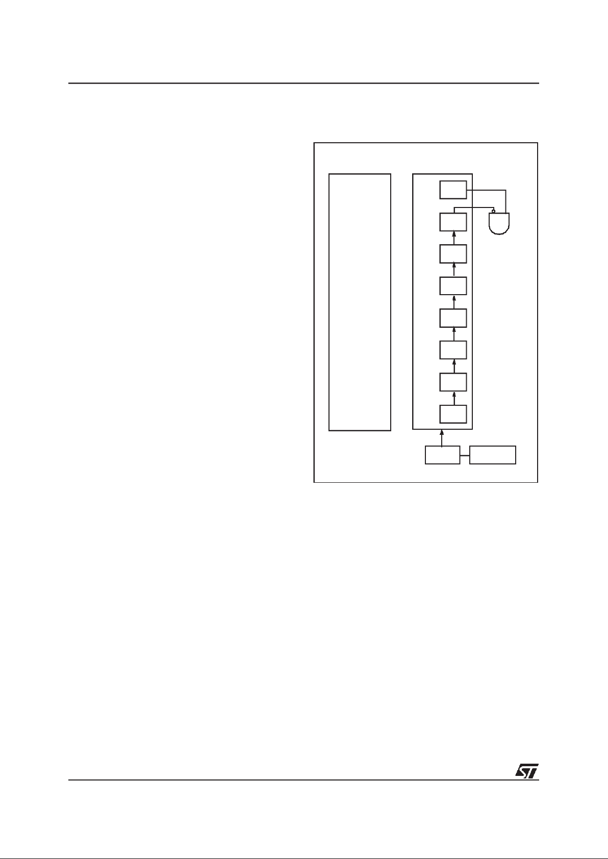
Figure 18. Digital Watchdog Block Diagram
NMI
SWITCH
I/O
VR02002
RSFF
8
DATA BUS
VA00010
-2
-12
OSCILLATOR
RESET
WRITE
RESET
DB0
R
S
Q
DB1.7 SETLOAD
7
8
-2
SET
CLOCK
44
Page 29

29/86
ST62T30B ST62E30B
3.4 INTERRUPTS
The CPU can manage four Maskable Interrupt
sources, in addition to a Non Maskable Interrupt
source (top priority interrupt). Each source is associated with a specific Interrupt Vector which contains a Jump instruction to the associated interrupt
service routine. These vectors are located in Program space (seeTable 9).
When an interrupt source generates an interrupt
request, and interrupt processing is enabled, the
PC register is loaded with the address of the interrupt vector (i.e. of the Jump instruction), which
then causes a Jump to the relevant interrupt service routine, thus servicing the interrupt.
Interrupt sources are linked to events either on external pins, or on chip peripherals. Several events
can be ORed on the same interrupt source, and
relevant flags are available to determine which
event triggered the interrupt.
The Non Maskable Interrupt request has the highest priority and can interrupt any interrupt routine
at any time; the other four interrupts cannot interrupt each other. If more than one interrupt request
is pending, these are processed by the processor
core according to their priority level: source #1 has
the higher priority while source #4 the lower. The
priority of each interrupt source is fixed.
Table 9. Interrupt Vector Map
3.4.1 Interrupt request
All interrupt sources but the Non Maskable Interrupt source can be disabled by setting accordingly
the GEN bit of the Interrupt Option Register (IOR).
This GEN bitalso defines if an interrupt source, including the Non Maskable Interrupt source, can restart the MCU from STOP/WAIT modes.
Interrupt request from the Non Maskable Interrupt
source #0islatched by a flip flop which is automat-
ically reset by the core at the beginning of the nonmaskable interrupt service routine.
Interrupt request from source #1 can be configured eitheras edge or level sensitive by setting accordingly the LES bit of the Interrupt Option Register (IOR).
Interrupt request from source #2 are always edge
sensitive. The edge polarity can be configured by
setting accordingly the ESB bit of the Interrupt Option Register (IOR).
Interrupt request from sources #3 & #4 are level
sensitive.
In edgesensitive mode, a latch is set when a edge
occurs on the interrupt source line and is cleared
when the associated interrupt routine is started.
So, the occurrence of an interrupt can be stored,
until completion ofthe running interrupt routine before being processed. If several interrupt requests
occurs before completion of the running interrupt
routine, only the first request is stored.
Storage ofinterrupt requests is not available in level sensitive mode. To be taken into account, the
low level must be present on the interrupt pin when
the MCU samples the line after instruction execution.
At the end of every instruction, the MCU tests the
interrupt lines: if there is an interrupt request the
next instruction is not executed and the appropriate interrupt service routine is executed instead.
Table 10.Interrupt Option Register Description
Interrupt Source Priority Vector Address
Interrupt source #0 1 (FFCh-FFDh)
Interrupt source #1 2 (FF6h-FF7h)
Interrupt source #2 3 (FF4h-FF5h)
Interrupt source #3 4 (FF2h-FF3h)
Interrupt source #4 5 (FF0h-FF1h)
GEN
SET Enable all interrupts
CLEARED Disable all interrupts
ESB
SET
Rising edge mode on interrupt source #2
CLEARED
Falling edge mode on interrupt source #2
LES
SET
Level-sensitive mode on interrupt source #1
CLEARED
Falling edge mode on interrupt source #1
OTHERS NOT USED
45
Page 30

30/86
ST62T30B ST62E30B
INTERRUPTS (Cont’d)
3.4.2 Interrupt Procedure
The interrupt procedure isvery similar to a call procedure, indeed the user can consider the interrupt
as an asynchronous call procedure. As this is an
asynchronous event, the user cannot know the
context and the time at which it occurred. As a result, the user should save all Data space registers
which may be used within the interrupt routines.
There are separate sets of processor flags for normal, interrupt and non-maskable interrupt modes,
which are automatically switched and so do not
need to be saved.
The following list summarizes the interrupt procedure:
MCU
– The interrupt is detected.
– The C and Z flags are replaced by the interrupt
flags (or by the NMI flags).
– The PC contents are stored in the first level of
the stack.
– The normal interrupt lines areinhibited (NMI still
active).
– The first internal latch is cleared.
–TheassociatedinterruptvectorisloadedinthePC.
WARNING: In some circumstances, when a
maskable interrupt occurs while the ST6 core is in
NORMAL mode and especially during the execution of an ”ldi IOR, 00h” instruction (disabling all
maskable interrupts): if the interrupt arrives during
the first 3 cycles of the ”ldi” instruction (which is a
4-cycle instruction) the core will switch to interrupt
mode BUT theflags CN and ZN will NOT switch to
the interrupt pair CI and ZI.
User
– User selected registers are saved within the in-
terrupt service routine (normally on a software
stack).
– The source of the interrupt is found by polling the
interrupt flags (if more than one source is associ-
ated with the same vector).
– The interrupt is serviced.
– Return from interrupt (RETI)
MCU
– Automatically the MCU switches backto the nor-
mal flag set (or the interrupt flag set) and pops
the previous PC value from the stack.
The interrupt routine usually begins by the identifying the device which generated the interrupt request (by polling). Theuser should save the registers which are used within the interrupt routine in a
software stack. After the RETI instruction is executed, the MCU returns to the main routine.
Figure 19.Interrupt Processing Flow Chart
INSTR UCTION
FETCH
INSTR UCTION
EXECUT E
INSTRUCTIO N
WAS
THE INSTRUCTI ON
ARETI ?
?
CLEAR
INTER RUPT MASK
SELECT
PROGRAM FLAGS
”POP”
THE STACK ED PC
?
CHE CK IF THERE IS
AN INTERR UPTREQUEST
AND INTERR UPT MASK
SELECT
INTERNAL MODE FLAG
PUSH THE
PC INTO THE STACK
LOAD PC FROM
INTERR UPT VECT OR
(FFC/FFD )
SET
INTER RUPT MASK
NO
NO
YES
IS THE CORE
ALREADY IN
NORMAL MODE?
VA000014
YES
NO
YES
46
Page 31

31/86
ST62T30B ST62E30B
INTERRUPTS (Cont’d)
3.4.3 Interrupt Option Register (IOR)
The Interrupt Option Register (IOR) is used to enable/disable the individual interrupt sources and to
select the operating mode of the external interrupt
inputs. This register is write-only and cannot be
accessed by single-bit operations.
Address: 0C8h — Write Only
Reset status: 00h
Bit 7, Bits 3-0 =
Unused
.
Bit 6 =
LES
:
Level/Edge Selection bit
.
When this bit is set to one, the interrupt source #1
is level sensitive. When cleared to zero the edge
sensitive mode for interrupt request is selected.
Bit 5 = ESB:
Edge Selection bit
.
The bit ESB selects the polarity of the interrupt
source #2.
Bit 4 =GEN:
Global Enable Interrupt
. When this bit
is set to one, all interrupts are enabled. When this
bit is cleared to zero all the interrupts (excluding
NMI) are disabled.
When the GEN bit is low, the NMI interrupt is active but cannot cause a wake up from STOP/WAIT
modes.
This register is cleared on reset.
3.4.4 Interrupt sources
Interrupt sources available on the
ST62E30B/T30B are summarized in theTable 11
with associated mask bit to enable/disable the interrupt request.
Table 11. Interrupt Requests and Mask Bits
70
- LES ESB GEN - - - -
Peripheral Register
Address
Register
Mask bit Masked Interrupt Source
Interrupt
source
GENERAL IOR C8h GEN
All Interrupts, excluding NM
I All
TIMER TSCR1 D4h ETI TMZ: TIMER Overflow source 4
A/D CONVERTER ADCR D1h EAI EOC: End of Conversion source 4
UART UARTCR D7h
RXIEN
TXIEN
RXRDY: Byte received
TXMT: Byte sent
source 4
ARTIMER
SCR1
SCR2
SCR3
SCR3
SCR3
E8h
E1h
E2h
E2h
E2h
OVFIEN
CP1IEN
CP2IEN
ZEROIEN
CMPIEN
OVFFLG: ARTIMER Overflow
CP1FLG
CP2FLG
ZEROFLG: Compare to zero flag
CMPFLG: Compare flag
source 3
SPI SPI DCh ALL End of Transmission source 1
Port PAn ORPA-DRPA C0h-C4h ORPAn-DRPAn PAn pin source 1
Port PBn ORPB-DRPB C1h-C5h ORPBn-DRPBn PBn pin source 2
Port PCn ORPC-DRPC C2h-C6h ORPCn-DRPCn PCn pin source 0
Port PDn ORPD-DRPD C3h-C7h ORPDn-DRPDn PDn pin source 2
47
Page 32

32/86
ST62T30B ST62E30B
IINTERRUPTS (Cont’d)
Interrupt Polarity Register (IPR)
Address: DAh — Read/Write
In conjunction with IOR register ESB bit, the polarity of I/O pins triggered interrupts can be selected
by setting accordingly the Interrupt Polarity Register (IPR). If a bit in IPR is set to one the corresponding port interrupt is inverted (e.g. IPR bit 2 =
1 ; port C generates interrupt on rising edge. At reset, IPRis cleared and all port interrupts are not inverted (e.g. Port C generates interrupts on falling
edges).
Bit 7 - Bit 4 =
Unused
.
Bit 3 =
Port D Interrupt Polarity
.
Bit 2 =
Port C Interrupt Polarity
.
Bit 1=
Port A Interrupt Polarity
.
Bit 0 =
Port B Interrupt Polarity
.
Tables 12. I/O Interrupts selections according to IPR, IOR programming
70
- - - - PortD PortC PortA PortB
GEN IPR3 IPR0 IOR5 Port B occurrence Port Doccurrence
Interrupt
source
1 0 0 0 falling edge falling edge
2
1 0 0 1 rising edge rising edge
1 0 1 0 rising edge falling edge
1 0 1 1 falling edge rising edge
1 1 0 0 falling edge rising edge
1 1 0 1 rising edge falling edge
1 1 1 0 rising edge rising edge
1 1 1 1 falling edge falling edge
0 X X X Disabled Disabled
GEN IPR1 IOR6 Port A occurrence
Interrupt
source
1 0 0 falling edge
1
1 0 1 low level
1 1 0 rising edge
1 1 1 high level
0 X X Disabled
IPR2 Port C occurrence Interrupt source
0 falling edge
0
1 rising edge
48
Page 33

33/86
ST62T30B ST62E30B
INTERRUPTS (Cont’d)
Figure 20. Interrupt Block Diagram
PORT C
PORT A
Bits
PBE
V
DD
FROM REGISTER PORT A,B,C,D,E
SINGLE BIT ENABLE
FF
CLK Q
CLR
I
0
Start
INT #0 NMI (FFC,D))
INT #2 (FF4,5)
PBE
Bits
NMI
PORT B
Bits
IPR Bit 2
FF
CLK Q
CLR
0
MUX
1
I
1
Start
IPR Bit 0
IOR bit 6(LES)
PBE
IPR Bit 1
FF
CLK Q
CLR
PBE
IPR Bit 3
IOR bit 5 (ESB)
I
2
Start
INT #1 (FF6,7)
INT #3 (FF2,3)
INT #4 (FF0,1)
IOR bit 4(GEN)
PORT D
Bits
CP1FLG
CP1IEN
CP2FLG
CP2IEN
OVFLG
OVFIEN
CMPFLG
CMPIEN
ZEROFLG
ZEROIEN
TMZ
ETI
EAI
EOC
RXRDY
RXIEN
TXMT
TXIEN
RESTART
STOP/WAIT
FROM
SPI
49
Page 34

34/86
ST62T30B ST62E30B
3.5 POWER SAVING MODES
The WAIT and STOP modes have been implemented in the ST62xx family of MCUs in order to
reduce the product’s electrical consumption during
idle periods. These two power saving modes are
described in the following paragraphs.
3.5.1 WAIT Mode
The MCU goes into WAIT mode as soon as the
WAIT instruction is executed. The microcontroller
can be considered as being in a “software frozen”
state where the core stops processing the program instructions, the RAM contents and peripheral registers are preserved as long as the power
supply voltage is higher than the RAM retention
voltage. In this mode the peripherals are still active.
WAIT mode can be used when the user wants to
reduce the MCU power consumption during idle
periods, while not losing track of time or the capability of monitoring external events. The active oscillator is not stopped in order to provide a clock
signal to the peripherals. Timer counting may be
enabled as well as the Timer interrupt, before entering the WAIT mode: this allows the WAIT mode
to be exited when a Timer interrupt occurs. The
same applies to other peripherals which use the
clock signal.
If the WAIT mode is exited due to a Reset (either
by activating the external pin or generated by the
Watchdog), the MCU enters a normal reset procedure. If an interrupt is generated during WAIT
mode, the MCU’s behaviour depends on the state
of the processor core prior to the WAIT instruction,
but also on the kind of interrupt request which is
generated. This is described in the following paragraphs. The processor core does not generate a
delay following the occurrence of the interrupt, because the oscillator clock is still available and no
stabilisation period is necessary.
3.5.2 STOP Mode
If the Watchdog is disabled, STOP mode is available. When in STOP mode, the MCU is placed in
the lowest power consumption mode. In this operating mode, the microcontroller can be considered
as being “frozen”, no instruction is executed, the
oscillator is stopped, the RAM contents and peripheral registers are preserved as long as the
power supply voltage is higher than the RAM retention voltage, and the ST62xx core waits for the
occurrence of an external interrupt request or a
Reset to exit the STOP state.
If the STOP state is exited due to aReset (by activating the external pin) the MCU will enter a normal reset procedure. Behaviour in response to interrupts depends on the state of the processor
core prior to issuing the STOP instruction, and
also on the kind of interrupt request that is generated.
This case will be described in the following paragraphs. The processor core generates a delay after occurrence of the interrupt request, in order to
wait for complete stabilisation of the oscillator, before executing the first instruction.
50
Page 35

35/86
ST62T30B ST62E30B
POWER SAVING MODE(Cont’d)
3.5.3 Exit from WAIT and STOP Modes
The following paragraphs describe how the MCU
exits from WAIT and STOP modes, when an interrupt occurs (not a Reset). It should be noted that
the restart sequence depends on the original state
of the MCU (normal, interrupt or non-maskable interrupt mode) prior to entering WAIT or STOP
mode, as well as on the interrupt type.
Interrupts do not affect the oscillator selection.
3.5.3.1 Normal Mode
If the MCU wasin the main routine when the WAIT
or STOP instruction was executed, exit from Stop
or Wait mode willoccur as soon as an interrupt occurs; the related interrupt routine is executed and,
on completion, the instruction which follows the
STOP or WAIT instruction is then executed, providing no other interrupts are pending.
3.5.3.2 Non Maskable Interrupt Mode
If the STOP or WAIT instruction has been executed during execution of the non-maskable interrupt
routine, the MCU exits from the Stop or Wait mode
as soon as an interrupt occurs: the instruction
which follows the STOP or WAIT instruction is executed, and the MCU remains in non-maskable interrupt mode, even if another interrupt has been
generated.
3.5.3.3 Normal Interrupt Mode
If the MCU was in interrupt mode before the STOP
or WAIT instruction was executed, it exits from
STOP or WAIT mode as soon as an interrupt occurs. Nevertheless, two cases must be considered:
– If the interrupt is anormal one, the interrupt rou-
tine in which the WAIT or STOP mode was en-
tered will be completed, starting with the
execution of the instruction which follows the
STOP or the WAIT instruction, and the MCU is
still in the interrupt mode. At the end of this routine pending interrupts will beserviced in accordance with their priority.
– In the event of a non-maskable interrupt, the
non-maskable interrupt service routine is processed first, then the routine inwhich theWAIT or
STOP mode was entered will be completed by
executing the instruction following the STOP or
WAIT instruction. The MCU remains in normal
interrupt mode.
Notes:
To achieve the lowest power consumption during
RUN or WAIT modes, the user program must take
care of:
– configuring unused I/Os as inputs without pull-up
(these should be externally tied to well defined
logic levels);
– placing all peripherals in their power down
modes before entering STOP mode;
When the hardware activated Watchdog is selected, or when the software Watchdog is enabled, the
STOP instruction is disabled and a WAIT instruction will be executed in its place.
If all interrupt sources are disabled (GEN low), the
MCU can only be restarted by a Reset. Although
setting GEN low does not mask the NMI as an interrupt, it will stop it generating a wake-up signal.
The WAIT and STOP instructions are not executed if an enabled interrupt request is pending.
51
Page 36

36/86
ST62T30B ST62E30B
4 ON-CHIP PERIPHERALS
4.1 I/O PORTS
The MCU features Input/Output lines which may
be individually programmed as any of thefollowing
input or output configurations:
– Input without pull-up or interrupt
– Input with pull-up and interrupt
– Input with pull-up, but without interrupt
– Analog input
– Push-pull output
– Open drain output
The lines are organised as bytewise Ports.
Each port is associated with 3 registers in Data
space. Each bit of these registers is associated
with a particular line (for instance, bits 0 of Port A
Data, Direction and Option registers are associated with the PA0 line of Port A).
The DATA registers (DRx), are used to read the
voltage level values of the lines which have been
configured as inputs, or to write the logic value of
the signal to be output on the lines configured as
outputs. The port data registers can be read to get
the effective logic levels of the pins, but they can
be also written by user software, in conjunction
with the related option registers, to select the different input mode options.
Single-bit operations on I/O registers are possible
but care is necessary because reading in input
mode is done fromI/O pins while writing willdirectly affect the Port data register causing an undesired change of the input configuration.
The Data Direction registers (DDRx) allow the
data direction (input or output) of each pin to be
set.
The Option registers (ORx) are used to select the
different port options available both in input and in
output mode.
All I/O registers can be read or written to just as
any other RAM location in Data space, so no extra
RAM cells are needed for port data storage and
manipulation. During MCUinitialization, all I/O registers are cleared and the input mode with pull-ups
and no interrupt generation is selected for all the
pins, thus avoiding pin conflicts.
Figure 21. I/O Port Block Diagram
V
DD
RESET
S
IN
CONTROLS
S
OUT
SHIFT
REGISTER
DATA
DATA
DIRECTION
REGISTER
REGISTER
OPTION
REGISTER
INPUT/OUTPUT
TO INTERRUPT
V
DD
TO ADC
VA00413
52
Page 37

37/86
ST62T30B ST62E30B
I/O PORTS (Cont’d)
4.1.1 Operating Modes
Each pin may be individually programmed as input
or output with various configurations.
This is achieved by writing the relevant bit in the
Data (DR), Data Direction (DDR) and Option registers (OR). Table 13 illustrates the various port
configurations which can be selected by user software.
4.1.1.1 Input Options
Pull-up, High Impedance Option. All input lines
can be individually programmed with or without an
internal pull-up by programming the OR and DR
registers accordingly. If the pull-up option is not
selected, the input pin will be in the high-impedance state.
4.1.1.2 Interrupt Options
All input lines can be individually connected by
software to the interrupt system by programming
the OR and DR registers accordingly. The interrupt trigger modes (falling edge, rising edge and
low level) can be configured by software as described in the Interrupt Chapter for each port.
4.1.1.3 Analog Input Options
Some pins can be configured as analog inputs by
programming the OR and DR registers accordingly. These analog inputs are connected to the onchip 8-bit Analog to Digital Converter.
ONLY ONE
pin should be programmed as an analog input at
any time, since by selecting more than one input
simultaneously their pins will be effectively shorted.
Table 13. I/O Port Option Selection
Note: X = Don’t care
DDR OR DR Mode Option
0 0 0 Input With pull-up, no interrupt
0 0 1 Input No pull-up, no interrupt
0 1 0 Input With pull-up and with interrupt
0 1 1 Input Analog input (when available)
1 0 X Output Open-drain output (20mA sink when available)
1 1 X Output Push-pull output (20mA sink when available)
53
Page 38

38/86
ST62T30B ST62E30B
I/O PORTS (Cont’d)
4.1.2 Safe I/O State Switching Sequence
Switching the I/O ports from one state to another
should be done in a sequence which ensures that
no unwanted side effects can occur. The recommended safe transitions are illustrated inFigure
22. All other transitions are potentially risky and
should be avoided when changing the I/O operating mode, as it is most likely that undesirable sideeffects will be experienced, such as spurious interrupt generation or two pins shorted together by the
analog multiplexer.
Single bit instructions (SET, RES, INC and DEC)
should be used with great caution on Ports Data
registers, since these instructions make an implicit
read and write back of the entire register. In port
input mode, however, the data register reads from
the input pins directly, and not from the data register latches. Since data register information in input
mode is used to set the characteristics of the input
pin (interrupt, pull-up, analog input), these may be
unintentionally reprogrammed depending on the
state ofthe input pins. As a general rule, it is better
to limit the use of single bit instructions on data
registers to when the whole (8-bit) port is in output
mode. In the case of inputs or of mixed inputs and
outputs, it is advisable to keep a copy of the data
register in RAM. Single bit instructions may then
be used on the RAM copy, after which the whole
copy register can be written to the port data register:
SET bit, datacopy
LD a, datacopy
LD DRA, a
Warning: Care must also be taken to not use instructions that act on a whole port register (INC,
DEC, or read operations) when all 8 bits are not
available on the device. Unavailable bits must be
masked by software (AND instruction).
The WAIT and STOP instructions allow the
ST62xx to be used in situations where low power
consumption is needed. The lowest power consumption is achieved by configuring I/Os in input
mode with well-defined logic levels.
The user must take care not to switch outputs with
heavy loads during the conversion of one of the
analog inputs in order to avoid any disturbance to
the conversion.
Figure 22. Diagram showing Safe I/O State Transitions
Note *. xxx = DDR, OR, DR Bits respectively
Interrupt
pull-up
Output
Open Drain
Output
Push-pull
Input
pull-up (Reset
state)
Input
Analog
Output
Open Drain
Output
Push-pull
Input
010*
000
100
110
011
001
101
111
54
Page 39

39/86
ST62T30B ST62E30B
I/O PORTS (Cont’d)
Table 14. I/O Port configuration for the ST62T30B/E30B
Note 1. Provided the correct configuration has been selected.
MODE AVAILABLE ON(1) SCHEMATIC
Input
(Reset state if PORT
PULL option disabled)
PA0-PA5
PB4-PB6
PC4-PC7
PD1-PD7
Input
with pull up
(Reset state if PORT
PULL option enabled)
PA0-PA5
PB4-PB6
PC4-PC7
PD1-PD7
Input
with pull up
with interrupt
PA0-PA5
PB4-PB6
PC4-PC7
PD1-PD7
Analog Input
PA4-PA5
PB4-PB6
PC4-PC7
PD1-PD7
Open drain output
5mA
Open drain output
20mA
PA4-PA5
PB4-PB6
PC4-PC7
PD1-PD7
PA0-PA3
Push-pull output
5mA
Push-pull output
20mA
PA4-PA5
PB4-PB6
PC4-PC7
PD1-PD7
PA0-PA3
Data in
Interrupt
Data in
Interrupt
Data in
Interrupt
Data out
ADC
Data out
VR01992A
55
Page 40

40/86
ST62T30B ST62E30B
I/O PORTS (Cont’d)
4.1.3 ARTimer alternate functions
As long as PWMEN (resp. OVFEN) bit is kept low,
the PA3/PWM (resp. PA2/OVF) pin is used as
standard I/Opin and therefore can be configured in
any mode through the DDR and OR registers.
If PWMEN (resp. OVFEN) bitis set,PA3/PWM (resp. PA2/OVF) pin must be configured as output
through the DDR and OR registers to be used as
PWM (OVF) output of the ARTimer16. All output
modes are available.
PA4/CP1 or PA5/CP2 pins must be configured as
input through DDR register to allow CP1 or CP2
triggered input capture of the ARTimer16. All input
modes are available and I/O’s can be read independently of the ARTimer at any time. As long as
RLDSEL2, RLDSEL1 bits do not enable CP1 or
CP2 triggered capture,PA4/CP1 and PA5/CP2 are
standard I/O’s configurable through DDR and OR
registers.
4.1.4 SPI alternate functions
PD2/Sin and PD1/Scl pins must be configured as
input through the DDR and OR registers to be
used as data in and data clock (Slave mode) for
the SPI. All input modes are available and I/O’s
can be read independently of the SPI at any time.
PD3/Sout must be configured in open drain output
mode to be used as data out for the SPI. In output
mode, the value present on the pin isthe port data
register content only if PD3 is defined as push pull
output, while serial transmission is possible only in
open drain mode.
4.1.5 UART alternate functions
PD4/RXD1 pin must be configured as input
through the DDR and OR registers to be used as
reception line for the UART. All input modes are
available and PD4 can be read independently of
the UART at any time.
PD5/TXD1 pin must be configured as output
through the DDR and OR registers to be used as
transmission line for the UART. Value present on
the pin in output mode is the Data register content
as long as no transmission is active.
56
Page 41

41/86
ST62T30B ST62E30B
I/O PORTS (Cont’d)
Figure 23. Peripheral Interface Configuration of SPI, UART and AR Timer16
PD4/RXD1
PID
0
MUX
1
PD5/TXD1
PD3/Sout
PD2/Sin
PD1/Scl
PA3/PWM
PA4/CP1
PA5/CP2
PA2/OVF
V
DD
DR
RXD
UART
IARTOE
TXD
PID
DR
PID
OPR
DR
1
MUX
0
OUT
IN
SYNCHRONOUS
SERIAL I/O
CLOCK
PID
DR
PID
DR
PP/OD
PID
DR
1
MUX
0
PWMEN
PWM
CP1
ARTIMER 16
CP2
OVFEN
OVF
PID
DR
PID
DR
PID
DR
1
MUX
0
VR01661D
57
Page 42

42/86
ST62T30B ST62E30B
I/O PORTS (Cont’d)
4.1.6 I/O Port Option Registers
ORA/B/C/D (CCh PA, CDh PB, CEh PC, CFh PD)
Read/Write
Bit 7-0 =
Px7 - Px0
:
Port A, B, C, and D Option
Register bits.
4.1.7 I/O Port Data Direction Registers
DDRA/B/C/D (C4h PA, C5h PB, C6h PC, C7h PD)
Read/Write
Bit 7-0 = Px7 - Px0:
Port A, B, C, and D Data Di-
rection Registers bits.
4.1.8 I/O Port Data Registers
DRA/B/C/D (C0h PA, C1h PB, C2h PC, C3h PD)
Read/Write
Bit 7-0 =
Px7 - Px0
:
Port A, B,C, and D Data Reg-
isters bits.
70
Px7 Px6 Px5 Px4 Px3 Px2 Px1 Px0
70
Px7 Px6 Px5 Px4 Px3 Px2 Px1 Px0
70
Px7 Px6 Px5 Px4 Px3 Px2 Px1 Px0
58
Page 43

43/86
ST62T30B ST62E30B
4.2 TIMER
The MCU features an on-chip Timer peripheral,
consisting of an 8-bit counter witha 7-bit programmable prescaler, giving a maximum count of 215.
The peripheral may be configured in three different
operating modes.
Figure 24 shows the Timer Block Diagram. The
external TIMER pin is available to the user. The
content of the 8-bit counter can be read/written in
the Timer/Counter register, TCR, while the state of
the 7-bit prescaler canbe read in the PSC register.
The control logic device is managed in the TSCR
register as described in the following paragraphs.
The 8-bit counter is decremented by the output
(rising edge) coming from the 7-bit prescaler and
can be loaded and read under program control.
When it decrements to zero then the TMZ (Timer
Zero) bit in the TSCR is set to “1”. If the ETI (Enable Timer Interrupt) bit in the TSCR is also set to
“1”, an interrupt request is generated as described
in the Interrupt Chapter. The Timer interrupt can
be used to exit the MCU from WAIT mode.
The prescaler input can be the internal frequency
f
INT
divided by 12 or an external clock applied to
the TIMER pin. The prescaler decrements on the
rising edge. Depending on the division factor programmed by PS2, PS1 and PS0 bits in the TSCR.
The clock input of thetimer/counter register is multiplexed to different sources. For division factor 1,
the clock input of the prescaler is also that of timer/counter; for factor 2, bit 0 of the prescaler register is connected to the clock input of TCR. This bit
changes its state at half the frequency of the prescaler input clock. For factor 4, bit 1 of the PSC is
connected to the clock input of TCR, and so forth.
The prescaler initialize bit, PSI, in the TSCR register must be set to “1” to allow the prescaler (and
hence the counter) to start. If it iscleared to “0”, all
the prescaler bits are set to “1” and the counter is
inhibited from counting. The prescaler can be
loaded with any value between 0 and 7Fh, if bit
PSI is set to “1”. The prescaler tap is selected by
means of the PS2/PS1/PS0 bits in the control register.
Figure 25 illustrates the Timer’s working principle.
Figure 24. Timer Block Diagram
DATABUS 8
8
8
8
8-BIT
COUNTER
6
5
4
3
2
1
0
PSC
STATUS/CONTROL
REGISTER
b7 b6 b5 b4 b3 b 2 b1 b0
TMZ ET I TOUT
DOUT
PSI
PS2
PS1 PS0
SELECT
1OF7
3
LATCH
SYNCHRONIZATION
LOGIC
TIMER
INTERRUPT
LINE
VA00009
:12
f
OSC
59
Page 44

44/86
ST62T30B ST62E30B
TIMER (Cont’d)
4.2.1 Timer Operating Modes
There are three operating modes, which are selected by the TOUT and DOUT bits (see TSCR
register). These three modes correspond to the
two clocks which can be connected to the 7-bit
prescaler (f
INT
÷ 12 or TIMER pin signal), and to
the output mode.
4.2.1.1 Gated Mode
(TOUT = “0”, DOUT = “1”)
In this mode the prescaler is decremented by the
Timer clock input (f
INT
÷ 12), but ONLY when the
signal on the TIMER pin is held high (allowing
pulse width measurement). This mode is selected
by clearing the TOUT bit in the TSCR register to
“0” (i.e. as input) and setting the DOUT bit to “1”.
4.2.1.2 Event Counter Mode
(TOUT = “0”, DOUT = “0”)
In this mode, the TIMER pin is the input clock of
the prescaler which is decremented on the rising
edge.
4.2.1.3 Output Mode
(TOUT = “1”, DOUT = data out)
The TIMER pin is connected to the DOUT latch,
hence the Timer prescaler is clocked by the prescaler clock input (f
INT
÷ 12).
The user can select the desired prescaler division
ratio through the PS2, PS1, PS0 bits. When the
TCR count reaches 0, it sets the TMZ bit in the
TSCR. The TMZ bit can be tested under program
control to perform a timer function whenever it
goes high. The low-to-high TMZ bit transition is
used to latch the DOUT bit of the TSCR and transfer it tothe TIMER pin. This operating mode allows
external signal generation on the TIMER pin.
Table 15. Timer Operating Modes
4.2.2 Timer Interrupt
When the counter register decrements tozero with
the ETI (Enable Timer Interrupt) bit set to one, an
interrupt request is generated as described in the
Interrupt Chapter. When the counter decrements
to zero, the TMZ bit in the TSCR register is set to
one.
Figure 25. Timer Working Principle
TOUT DOUT Timer Pin Timer Function
0 0 Input Event Counter
0 1 Input Gated Input
1 0 Output Output “0”
1 1 Output Output “1”
BIT0 BIT1 BIT2 BIT3 BIT6BIT5BIT4
CLOCK
7-BIT PRESCALER
8-1 MULTIPLEXER
8-BIT COUNTER
BIT0 BIT1 BIT2 BIT3 BIT4 BIT5
BIT6
BIT7
10
2
34 56 7
PS0
PS1
PS2
VA00186
60
Page 45

45/86
ST62T30B ST62E30B
TIMER (Cont’d)
4.2.3 Application Notes
The user can select the presence of an on-chip
pull-up on the TIMER pin as option.
TMZ isset when thecounter reaches zero; however, it may also be set by writing 00h in the TCR
register or by setting bit 7 of the TSCR register.
The TMZ bit must be cleared by user software
when servicing the timer interrupt to avoid undesired interrupts when leaving the interrupt service
routine. After reset, the 8-bit counter register is
loaded with 0FFh, while the 7-bit prescaler isloaded with 07Fh, and the TSCR register is cleared.
This means that the Timer is stopped (PSI=“0”)
and the timer interrupt is disabled.
If the Timer is programmed in output mode, the
DOUT bit is transferred to the TIMER pin when
TMZ is set to one (by software or due to counter
decrement). When TMZ is high, the latch is transparent and DOUT iscopied to the timer pin. When
TMZ goes low, DOUT is latched.
A write to the TCR register will predominate over
the 8-bit counter decrement to 00h function,i.e. if a
write and a TCR register decrement to 00h occur
simultaneously, the write will take precedence,
and the TMZ bit is not set until the 8-bit counter
reaches 00h again. The values of the TCR and the
PSC registers can be read accurately at any time.
4.2.4 Timer Registers
Timer Status Control Register (TSCR)
Address: 0D4h — Read/Write
Bit 7 = TMZ:
Timer Zero bit
A low-to-high transition indicates that the timer
count register has decrement tozero. This bitmust
be cleared by user software before starting a new
count.
Bit 6 = ETI:
Enable Timer Interrupt
When set, enables the timer interrupt request. If
ETI=0 the timer interrupt is disabled. If ETI=1 and
TMZ=1 an interrupt request is generated.
Bit 5 =
TOUT
:
Timers
Output Control
When low, this bit selects the input mode for the
TIMER pin. When high the output mode is selected.
Bit 4 = DOUT:
Data Output
Data sent to the timer output when TMZ is set high
(output mode only). Input mode selection (input
mode only).
Bit 3 = PSI:
Prescaler Initialize Bit
Used to initialize the prescaler and inhibitits counting. When PSI=“0” the prescaler is set to 7Fh and
the counter is inhibited. When PSI=“1” the prescaler is enabled to count downwards. As long as
PSI=“0” both counter and prescaler are not running.
Bit 2, 1, 0 =
PS2, PS1, PS0
:
Prescaler Mux. Se-
lect.
These bits select the division ratio ofthe pres-
caler register.
Table 16. Prescaler Division Factors
Timer Counter Register TCR
Address: 0D3h — Read/Write
Bit 7-0 =D7-D0:
Counter Bits.
Prescaler Register PSC
Address: 0D2h — Read/Write
Bit 7 = D7: Always read as “0”.
Bit 6-0 =
D6-D0
: Prescaler Bits.
70
TMZ ETI TOUT DOUT PSI PS2 PS1 PS0
PS2 PS1 PS0 Divided by
0001
0012
0104
0118
10016
10132
11064
1 1 1 128
70
D7 D6 D5 D4 D3 D2 D1 D0
70
D7 D6 D5 D4 D3 D2 D1 D0
61
Page 46

46/86
ST62T30B ST62E30B
4.3 ARTIMER 16
The ARTIMER16 is a timer module based on a 16
bit downcounter with Reload, Capture and Compare features to manage timing requirements. Two
outputs provide PWM and Overflow (OVF) output
signals each with programmable polarity, and two
inputs CP1 and CP2 control start-up, capture
and/or reload operations on the central counter.
The ARTIMER16 includes four 16-bit registers
CMP,RLCP,MASK and CP for the Reload, Capture and compare functions, four 8-bit status/control registers and the associated control logic.The
16-bit registers are accessed from the 8-bit internal bus. The full 16-bit word iswritten in two bytes,
the high byte first and then the low byte. The high
byte is stored in an intermediate register and is
written to the target 16-bit register at the same
time as the write to the low byte. This high byte will
remain constant if further writes are made to the
low bytes, until the high byte is changed. Full
Read/Write access is available to all registers except where mentioned.
The ARTIMER16 may be placed into the reset
mode by resetting RUNRES to 0 in order to
achieve lower consumption. The contents of
RLCP, CP, MASK and CMP are not affected, nor
is the previous run mode of the timer changed. If
RUNRES is subsequently set to 1, the timer restarts in the same RUN mode as previously set if
no changes are made to the timer status registers.
Finally, interrupt capabilities are associated to the
Reload, Capture and Compare features.
Figure 26. ARTIMER16 Block Diagram
SCR1
SCR2
SCR3
SCR4
BUS INTERFACE
8-Bit MCU DATA BUS
16-Bit D ATA BUS
8
8
8
4
8
16
16
16
CMP
MASK
RLCP
CP
16
16
COUNTER
CONTROL LOGIC
Compare-to-0
Compare
PSC
f
INT
PWM
OVF
CP1
CP2
INT
16-Bit
16-Bit
16-Bit
16-Bit
VR02014
62
Page 47

47/86
ST62T30B ST62E30B
4.3.1 CENTRAL COUNTER
The core of the 16 bit Auto-Reload Timer is a 16bit synchronous downcounter which accepts the
MCU internal clock through a prescaler with a programmable ratio (1/1, 1/4, 1/16).
The maximum time for downcounting is therefore
216x Psc x Tclk where Psc is the prescaler ratio,
and Tclk the period of the main oscillator.
This down counter is stopped and its content kept
cleared as long as RUNRES bit is cleared.
4.3.1.1 Reload functions
The 16-bit down counter can be reloaded 3 different ways:
At a zero overflow occurrence with thebitRELOAD
cleared: The counter is reloaded to FFFFh.
At a zero overflow occurrence with the bit
RELOAD set: The counter isreloaded with the value programmed in the RLCP register. For each
overflow, the transition between 0000h and the reload value (RLCP or FFFFh) is flagged through the
OVFFLG bit.
At an external event on pin CP1or CP2with the bit
RELOAD set: The counter isreloaded with the value programmed in the RLCP register.
As a consequence, the time between a timer reload and a zero overflow occurrence depends on
the value in RLCP when RELOAD bit is set. This
time is equal to (RLCP+1) x Psc x Tclk when
RELOAD bitis set, while it is 216x Psc x Tclk when
RELOAD bit is cleared.
4.3.1.2 Compare functions
The value in the counter CT is continuously compared to 0000h and to the value programmed into
the Compare Register CMP. The comparison
range to 0000h and CMP is defined by using the
MASK register to select which bitsare used, therefore the comparisons performed are:
– MASK&CT =?MASK&CMP.
– MASK&CT =?0000h.
When a matched comparison to 0000h or
MASK&CMP occurs, the flags ZEROFLG and
COMPFLG are respectively set.
By using MASK values reported inTable 17, the
MASK register works as counter frequency multiplier for the compare functions. In that case positive masked comparison occur with a period of
2
(n+1)
x Psc x Tclk where n is the position of the
most significant bit of MASK value.
Table 17. Recommended Mask Values
Note: Writing 0000h in MASK gives a period equal
to two times the prescaled period Psc xTclk.
Figure 27. Flags Setting in Compare and Reload Functions
Hexadecimal Binary
MSbit at 1
position,n
FFFFh
7FFFh
3FFFh
1FFFh
0FFFh
...
0007h
0003h
0001h
1111 1111 1111 1111
0111 1111 1111 1111
0011 1111 1111 1111
0001 1111 1111 1111
0000 1111 1111 1111
...
0000 0000 0000 0111
0000 0000 0000 0011
0000 0000 0000 0001
15
14
13
12
11
2
1
0
CMP
Counter
ZEROFLG
0
FFFFh
or
RLCP
Software Reset
Software Reset
Software Reset
OVFFLG
COMPFLG
Value CT
63
Page 48

48/86
ST62T30B ST62E30B
CENTRAL COUNTER(Cont’d)
4.3.1.3 Capture functions
Content of the counter CT can always be downloaded (captured) into the CP register at selectable event occurrence on pins CP1 and CP2, while
capture in RLCP is possible only when the bit
RELOAD is cleared.
Capture functions with RELOAD cleared are used
for period or pulse width measurements with input
CP2, or for phase measurements between two
signals on CP1 and CP2, with the counter in free
running mode. In these modes, counter values by
the two events occurence are stored into RLCP
and CP and the counter remains in free running
mode.
Capture functions with RELOAD set, are used for
same application purpose, but in that case, the
first event reloads the counter from RLCP while
the second event captures the counter content
into the CP register. Therefore, the counter is not
in free running mode for other functions since the
down counting start is initiated byeither CP1, CP2
or RUNRES event according to RLDSEL1 and
RLDSEL2 bit.
4.3.2 SIGNAL GENERATION MODES
4.3.2.1 Output modes
Any positive comparison to 0000h or
MASK&CMP, and any overflow occurence can be
used to control the OVF or PWM output pins in
various modes defined bybits OVFMD, PWMPOL,
PWMEN and PWMMD.
PWM pin output modes
OVF pin output modes
* The OVF pin is reset by clearing the flag OVFFLG.
4.3.2.2 Frequency and duty cycles on PWM
pins
In Set/Resetmode (PWMMD=0), theperiod onthe
PWM pin is the time between two matched
masked comparison to 0000h, at which PWM pin
is set (PWMPOL=1) or reset (PWMPOL=0). As
long as no reload function from RLCP is performed
(RELOAD bit cleared) and no mask is used, this
value is 216x Psc xTclk. If, on the contrary, reload
function or a mask are used, the frequency is controlled through the RLCP and MASK values (Figure 28). The condition to reset (PWMPOL=1) or
set back (PWMPOL=0) PWM pin is a matched
masked comparison to CMP. Given a RLCP and
MASK values within the Table 17, CMP defines
the duty cycle.
In Toggle mode (PWMMD=1), PWM pin changes
of state at each positive masked comparison to
CMP value. The frequency is half the frequency in
Set/Reset mode and the duty-cycle isalways 50%.
4.3.2.3 Frequency and duty cycles on OVF pin
OVF pinactivation is directed by thetimer overflow
occurence and therefore its frequency depends
only of the downcounting time from the reload value to 0000h. This means its period is equal to T=
(RLCP+1) x Psc x Tclk in Set/Reset mode and 2 x
(RLCP+1) x Psc x Tclk in Toggle mode.
Duty cycle is controlled in Set/Reset mode
(OVFMD cleared) by software, since OVF pin can
be reset only by clearing the OVFFLG bit. In toggle
mode (OVFMD set), the duty cycle is always 50%.
Table 18. Achievable periods on PWM pin
Note
: n is the position of the most significant bit of MASK value.
MASK & CNT
= 0000h
x x no yes no yes X
MASK&CT=
MASK&CMP
x x yes no yes no yes
PWMEN 0 0 1 1 1 1 1
PWMMD X X 0 0 0 0 1
PWMPOL 0 1 0 0 1 1 X
PWM pin 0 1 Reset Set Set Reset Toggle
Zero overflow (OVFFLG) 1 1
OVFMD 0 1
OVF pin Set* Toggle
Mask value FFFFh xxxxh
Period in Set/Reset mode (PWMMD=0) (RLCP+1) x Psc x Tclk 2
(n+1)
x Psc x Tclk
Period in Toggle mode (PWMMD=1) 2 x (RLCP+1) x Psc x Tclk 2 x 2
(n+1)
x Psc x Tclk
64
Page 49

49/86
ST62T30B ST62E30B
Figure 28. Mask Impact on the Compare Functions in PWM mode (PWMD=0, PWMPOL=1)
FEDCBA9876543210F
MASK
000Fh
0007h
0003h
0001h
CMP = 000Fh
Counter
24/f
CLK
most
significant
“1” is bit 3
23/f
CLK
“1” is bit 2
22/f
CLK
“1” is bit 1
21/f
CLK
“1” is bit 0
most
most
most
0003&000C = 0000h
0003&0007 = 0003&000F
significant
significant
significant
Bit 0...3
65
Page 50

50/86
ST62T30B ST62E30B
4.3.3 TIMINGS MEASUREMENT MODES
These modes are based on the capture of the
down counter content into either CP or RLCP registers. Some are used in conjunction with a synchronisation of the down counter by reload functions on external event on CPi pins or software
RUNRES setting, while other modes do not affect
the downcounting. As long as RELOAD bit is
cleared, the down counter remains in free running
mode.
4.3.3.1 Timing measurement with startup
control
Three startup conditions, selected by RLDSELi bit
can reload the counter from RLCP and initiate the
down counting when RELOAD bit is set. The first
mode is software controlled through the RUNRES
bit,whilethetwo others are basedonexternalevent
on pins CP1 and CP2 with configurable polarities.
External event on CP2 pin (with configurable polarities) is used as strobe to launch the capture of
the CT counter into CP. When RELOAD bit is set,
RLCP cannot be used for capture, sinceit contains
the reload value..
Finally, 3 different Reload/Capture sequences are
available:
– CP1 triggered restart mode with CP2 event de-
tection.
– CP2 triggered restart mode with second CP2
event detection.
– Software triggered restart mode with CP2 event
detection.
CP1 triggered restart mode with CP2 event detection.
This mode is enabled for RLDSEL2=0 and
RLDSEL1=1.
External events on CPi pins are enabled as soon as
RUNRES bit is set, whichletsthe prescaler andthe
downcounterrunning.Thenextactiveedge on CP1
causes the counter to be loaded from RLCP, the
CP1FLG tobeset andthedowncounting startsfrom
RLCP value.EachfollowingactiveedgeonCP1will
causeareload ofthecounter.If CP1FLG isnotreset
beforethenextreload,theCP1ERRflagissetatthe
same time as the counter is reloaded. Both flags
should then be cleared by software.
While the counter is counting, any active edge on
CP2 will capture the value of the counter at that instant intothe CP Register and set the CP2FLG bit.
If CP2FLG is not cleared before the following CP2
event, the CP2ERR flagbit is set, and no new capture can be performed
Capturing is re-enabled by clearing both CP2FLG
and CP2ERR.
Ifacapture on CP2and a reload onCP1occuratthe
same time, thecaptureofthecountertoCPis made
first, and thenthe counter is reloaded from RLCP.
Figure 29. CP1 Triggered Restart Mode with CP2 Event Detection
RELOAD
1 Reload on CP1,CP2, RUNRES / Capture CP2
0 Capture CP1 / Capture CP2
VR02007
COUNTER
CP1
Set CP1FLG Set CP1ERR
0000h 0000h
CT
Disabled
Enable the Inputs
RUNRES
Software Reset
Reload and Start
Reload Reload
Set CP1FLG
Disabled
Set CP2ERR
Disabled Capture CT into CP
Set CP2FLG
CP2
DisabledFirst Capture in CP
Then Reload
Set CP1ERR, CP2FLG
Clear all Flags
66
Page 51

51/86
ST62T30B ST62E30B
TIMINGS MEASUREMENT MODES(Cont’d)
CP2 triggered restart mode with CP2 event de-
tection.
This mode is enabled for RLDSEL2=1 and
RLDSEL1=0.
As long as RUNRES bit is set, an external event
on CP2pin generates both, at first the capture into
CP, and then the reload from RLCP. Capture into
CP on CP2 event is e nabled only if CP2FLG and
CP2ERR are cleared, otherwise only reload functions from RLCP are performed.
An external event on CP1 activates CP1FLG or
CP1ERR flags without any impact on the reload or
capture functions.
Note: After Reset, the first CP2 event will capture
the 0000h state of the counter into CP and then
will restart the counter after loading it from RLCP.
CP2FLG flag must always be cleared to execute
another capture into CP.
Software triggered restart mode with CP2
event detection.
This mode is enabled for RLDSEL2=0 and
RLDSEL1=0.
RUNRES bit setting initiates the reload and startup
of the downcounting, while CP2 is used as strobe
source for the CT capture into CP register.
Figure 30. CP2 Triggered Restart Mode with CP2 Event Detection
Figure 31. Software Triggered Restart Mode with CP2 Event Detection
VR02007C
CP1
No action
Set CP2ERR
First Capture CT into CP
CP2
Set CP1ERRSet CP1FLG
Reload CT from RLCP
Then Reload CT from RLCP
Set CP2FLG
Reload CT from RLCP
VR02007D
COUNTER
CP1
CP1 disabled
0000h 0000h
CT
Load Counter from RLCP and Startup
RUNRES
Software Reset
Set CP1FLG
CP2 disabled
CP2
Set CP2ERR
CP1 disabled
Set CP1ERR
Capture CT into CP
Set CP2FLG
67
Page 52

52/86
ST62T30B ST62E30B
TIMINGS MEASUREMENT MODES(Cont’d)
4.3.3.2 Timing measurement without startup
control
The down counter is in free running mode with
RUNRES bit set and RELOAD bit cleared. This
means counter automatically restarts from FFFFh
on zero overflow and signal generation on PWM
and OVF pins is not affected.
Two independent capture paths exist to CP and
RLCP, which are both Read only registers. CP1 is
the source (Configurable polarity) for a capture
into RLCP while CP2 is the source (Configurable
polarity) of a capture into CP.
Independently of CP2 signal, if CP1FLG and
CP1ERR are cleared, the first active edge on CP1
will trigger a capture into RLCP, triggering
CP1FLG. As long as CP1FLG has not been
cleared, a second following active edge will trig
CP1ERR without any capture into neither RLCP
nor CP.
Independently of CP1 signal, if CP2FLG and
CP2ERR are cleared, the first active edge on CP2
will trigger a capture into CP, triggering CP2FLG.
As long as CP2FLG has not been cleared, a sec-
ond following active edge will trig CP2ERR without
any capture into neither RLCP or CP.
4.3.4 INTERRUPT CAPABILITIES
The interrupt source latches of the ARTIMER16
are always enabled and set any time the interrupt
condition occurs.
The interrupt output is a logical OR of five logical
ANDs:
– INT = [(CP1FLG & CP1IEN)
– OR (CP2FLG & CP2IEN)
– OR(OVFFLG & OVFIEN)
– OR(COMPFLG & CMPIEN)
– OR (ZEROFLG & ZEROIEN)]
Thus, if any enable bit is 1, the interrupt output of
the ARTIMER16 goes high when the respective
flag is set. If no enable bit is 1, and one of the interrupt flags is set, the interrupt output remains 0,
but if the respective enable bit isset to 1 through a
write operation, the interrupt output will go high,
signalling the interrupt to the Core.
Figure 32. Positive CP1 - to negative CP2-Edge Measurement (CP1POL = 1, CP2POL = 0)
Application Note:
Depending on polarity setting for CP1/CP2, and of
CP1/CP2 connections, phase, period and pulse
width measurements can be achieved. The total
independence between CP1 and CP2 captures allows phase detection by measuring which of
CP1FLG or CP2FLG is setat first following a reset
of these flags.
VR02006F
COUNTER
CP1
CP2
Capture into RLCP
Set CP1FLG
Set CP1ERR
Set CP2FLG
Capture into CP
Set CP2ERR
CP1=CP2 CP1POL=CP2POL Measurement
Yes Yes Period
Yes No Pulse width
No X Phase
68
Page 53

53/86
ST62T30B ST62E30B
4.3.5 CONTROL REGISTERS
Status Control Register 1 (SCR1)
Address: E8h - Read/Write/Clear only
Bits 7 & 6 =
PSC2..PSC1
.
Clock Prescaler
. These
bits define the prescaler options for the prescaler
to the Counter Register according to the following
table.
The Prescaler must be disabled (PSC2 = 0, PSC1
= 0) before a new prescaler factor is set if the
counter is running (after a hardware reset the
prescaler is automatically disabled).
To avoid inconsistencies in timing, the prescaler
factor should be set first, and then the counter
started.
Bit 5 = RELOAD. Reload enabled. When set this
bit enables reload from RLCP register into CT register. On the contrary, if RELOAD is cleared,
RLCP is used as target for capture from the counter CT register.
Bit 4 =
RUNRES
.
Run/Reset
. This bit enables the
RUN or RESET operation of the ARTIMER.
If 0, the counter CT is cleared to zero, and is
stopped. Setting this bit to 1 permits the startup of
the counter, and enables the synchronisation circuits for the timer inputs CP1 and CP2.
Bit 3 =
OVFIEN
.
Overflow Int. Enable
. The Overflow Interrupt is masked when this bit is 0.
Setting the bit to 1 enables the overflow flag to set
the ARTIMER interrupt.
Bit 2 = OVFFLG. When this bit is 0, no overflow
has occurred since the last clear of this bit. If the
bit is at 1, an overflow has occurred.
This bit cannot be set by program, only cleared.
Bit 1 = OVFMD. The Overflow Output mode is set
by this bit; when 0, the overflow output is run in set
mode (OVF will be set on the first overflow event,
and will bereset when OVFFLG iscleared). When
1 the overflow output is in toggle mode; OVF toggles its state on every overflow event (independent to the state of OVFFLG).
Bit 0 = This bit is reserved and must be set to 0.
Status Control Register 2 (SCR2)
Address: E1h - Read/Write/Clear only
Bit 7 = Reserved. Must be kept cleared.
Bit 6 =
CP1ERR
.
CP1 Error Flag
. This bit is set to
1 if a new CP1 event has taken place since
CP1FLG was set to signal an errorcondition, itis 0
if there has been no event.
It is recommended to clear CP1ERR at any time
that CP1FLG is cleared, as further CP1 events
cannot be recognised if CP1ERR is set. This bit
cannot bet set by write, only cleared.
Bit 5 =
CP2ERR
.
CP1 Error Flag
. This bit is set to
1 if a new CP2 event has taken place since
CP2FLG was set to signal an errorcondition, itis 0
if there has been no event.
It is recommended to clear CP2ERR at any time
that CP2FLG is cleared, as further CP2 events
cannot be recognised if CP2ERR is set. This bit
cannot bet set by write, only cleared.
Bit 4 = CP1IEN.
CP1 Interrupt Enable
.CP1The
Capture 1 Interrupt is masked when this bit is 0.
Setting the bit to 1 enables the CP1 event flag
CP1FLG to set the ARTIMER interrupt.
Bit 3 = CP1FLG.
CP1 Interrupt Flag
. When this bit
is 0, no CP1 event has occurred since the last
clear of this bit. If the bit is at 1, a CP1 event has
occurred.
This bit cannot be set by program, only cleared.
Bit 2 = CP1POL.
CP1 Edge Polarity Select
.
CP1POL defines the polarity for triggering the CP1
event.
A 0 defines the action on a falling edge on the CP1
input, a 1 on a rising edge.
Bit 1 & 0 =
RLDSEL2..RLDSEL1
.
Reload Source
Select
. These bits define the source for the reload
events; they do not affect theoperation of the capture modes.
70
PSC 2 PSC 1 RELOAD RUNRES OVFIEN OVFFLG OVFMD -
PSC2 PSC1 Function
00
Clock Disabled (prescaler and counter
stopped
0 1 Prescale by 1
1 0 Prescale by 4
1 1 Prescale by 16
70
- CP1ERR CP2ERR CP1IEN CP1 F LG CP1POL RLDSEL2 RLDSEL1
RLDSEL2 RLDSEL1 Function
00
Reload and startup triggered by
RUNRES
01
Reload triggered by every CP1
event
10
Reload triggered by every CP2
event
1 1 Reload disabled
69
Page 54

54/86
ST62T30B ST62E30B
CONTROL REGISTERS(Cont’d)
Status Control Register 3 (SCR3)
Address: E2h - Read/Write/Clear only
Bit 7 = CP2POL.
CP2 Edge Polarity Select
.
CP2POL defines the polarity for triggering the CP2
event.
A 0 defines the action onafalling edge on the CP2
input, a 1 on a rising edge.
Bit 6 = CP2IEN.
CP2 Interrupt Enable
. The Capture 2 Interrupt is masked when this bit is 0. Setting the bit to 1 enables the CP2 event flag
CP2FLG to set the ARTIMER interrupt.
Bit 5 =
CP2FLG
.
CP2 Interrupt Flag
. When this bit
is 0, no CP2 event has occurred since the last
clear of this flag. If the bit is at 1, the first CP2
event and capture into CP has occurred.
This bit cannot be set by program, only cleared.
Bit 4 = CMPIEN.
Compare Int. Enable
. The Compare Interrupt is masked when this bit is 0.
Setting the bit to 1 enables the Compare flag
CMPFLG to set the ARTIMER interrupt.
Bit 3 =
CMPFLG
.
Compare Flag
. When this bit is
0, no Masked-Compare True event has occurred
since the last clear of this flag. If the bit is at 1, a
Masked-Compare event has occurred.
This bit cannot be set by program, only cleared.
Bit 2 = ZEROIEN.
Compare to Zero Int Enable.
The Masked-Counter Zero Interrupt is masked
when this bit is 0. Setting the bit to 1 enables the
ZEROFLG flag to set the ARTIMER interrupt.
Bit 1 =
ZEROFLG
.
Compare to Zero Flag
. When
this bit is 0, no Masked-Counter Zero event has
occurred since the last clear of this flag. If the bit is
at 1, a Masked-Counter Zero event has occurred
as the Masked Counter state equals 0 when running or on hold (not on Reset).
Bit 0 =
PWMMD
.
PWM Output Mode Control
.The
PWM Output mode is set by this bit; when 0, the
PWM output is run in set/reset mode (the PWM
output is set on a Masked-Counter Zero event and
is reset when on a Masked-Compare event).
When 1 the PWM output is in toggle mode; PWM
toggles its state on every Masked-Compare event.
Notes:
A Masked-Compare isthe logical AND of the Mask
Register MASK with the Counter Register CT,
compared with the logical AND of the compare
Register CMP: [(MASK & CT) = (MASK&CMP)].
A Masked-Counter Zero is the logical AND of the
Mask Register MASK with the Counter Register
CT, compared with zero: [(MASK & CT) = 0000h]
70
CP2 P OL CP2 I EN CP2FL G CMPI E N CMF L G ZER O IE N ZERO F L G PWMM D
70
Page 55

55/86
ST62T30B ST62E30B
CONTROL REGISTERS(Cont’d)
Status Control Register 4 (SCR4)
Address: E3h - Read/Write/Clear only
Bit7- Bit4 = Reserved, set to 0.
Bit 3 =OVFPOL.
Overflow Output Polarity
. This bit
defines the polarity for the Overflow Output OVF.
When 0, OVF is set on every overflow event if enabled in Set mode (OVFEN = 1, OVFMD = 0). The
reset state of OVF is 0.
When 1, OVF is reset on every overflow event if
enabled in Set mode.
The reset state of OVF is 1.
Bit 2 = OVFEN.
Overflow Output Enable
. This bit
enables the Overflow output OVF. When 0 the
Overflow output is disabled: if OVFPOL = 0, the
state of OVF is 0, if OVFPOL = 1, the state of
OVF = 1.The Overflow Output is enabled when
this bit =1, it must be setto use the OVF output.
Bit 1 = PWMPOL.
PWM Output Polarity.
This bit
defines the polarity for the PWM Output PWM.
When 0, PWM is set on every Masked-Counter
Zero event and is reset on a Masked-Compare if
enabled in Set/Reset mode (PWMEN = 1, PWMMD = 0).
The reset state of PWM pin is 0 When 1, OVF is
set on every Masked-Compare event and is reset
on a Masked-Counter Zero event if enabled in
Set/Reset mode (PWMEN = 1, PWMMD = 0).
The reset state of PWM is 1.
Bit 0 = PWMEN.
PWM Output Enable.
This bit enables the PWM output PWM. When 0 the PWM
output is disabled: if PWMPOL = 0, the state of
PWM is 0, if PWMPOL = 1, the state of PWM = 1.
The PWM Output is enabled when this bit = 1, it
must be set to use the PWM output.
Notes:
A Masked-Compare is the logical AND of the Mask
Register MASK with the Counter Register CT,
compared with the logical AND of the compare
Register CMP: [(MASK & CT) = (MASK&CMP)].
A Masked-Counter Zero is the logical AND of the
Mask Register MASK with the Counter Register
CT, compared with zero: [(MASK & CT) = 0000h].
4.3.6 16-BIT REGISTERS
Note: Care must be taken when using single-bit
instructions (RES/SET/INC/DEC) 16-bit registers
(RLCP, CP, CMP, MSK) since these instructions
imply a READ-MODIFY-WRITE operation on the
register. As the ST6 is based on a 8-bit architecture, to write a 16-bit register, the high byte must
be written first to an intermediate register (latch
register) and the whole 16-bit register is loaded at
the same time as the low byte is written. A WRITE
operation of the HIGH byteis performed on the intermediate register (latch register) but aREAD operation of the HIGH byte is directly performed on
the 16-bit register (last loaded value). As a consequence, it is always mandatory to write the LOW
byte before any single-bit instruction on the HIGH
byte in order to load the value set inthe intermediate register to the16-bit register (refresh the 16-bit
register).
Example:
The following sequence is NOT GOOD:
ldi t16cmph, 055h
ldi t16cmpl, 000h
; t16cmp (16-bit register)=5500h
ldi t16cmph, 0AAh
; t16cmp (16-bit register)=5500h
inc t16cmph
; t16cmp (16-bit register)=5500h
ldi t16cmpl, 000h
; t16cmp (16-bit register)=5600h
; and NOT AB00h
The CORRECT sequence is:
ldi t16cmph, 055h
ldi t16cmpl, 000h
; t16cmp (16-bit register)=5500h
ldi t16cmph, 0AAh
; t16cmp (16-bit register)=5500h
ldi t16cmpl, 000h
; t16cmp (16-bit register)=AA00h
inc t16cmph
; t16cmp (16-bit register)=AA00h
ldi t16cmpl, 000h
;t16cmp (16-bit register )=AB00h
70
Res. Res. Res. Res.
OVFPO
L
OVFEN PMPOL
PWME
N
71
Page 56

56/86
ST62T30B ST62E30B
Reload/Capture Register High Byte (RLCP)
Address: E9h - Read/ (Write if RELOAD bit set)
D7-D0. These bits are the High byte (D15-D8) of
the 16-bit Reload/Capture Register.
Reload/Capture Register Low Byte (RLCP)
Address: EAh - Read/ (Write if RELOAD bit set)
D7-D0. These bits are the Low byte (D7-D0) of the
16-bit Reload/Capture Register.
Capture Register High Byte (CP)
Address: EBh - Read Only
D7-D0. These bits are the High byte (D15-D8) of
the 16-bit Capture Register.
Capture Register Low Byte (CP)
Address: ECh - Read Only
D7-D0. These bits are the Low byte (D7-D0) of the
16-bit Capture Register.
Compare Register High Byte (CMP)
Address: EDh - Read/Write
D7-D0. These bits are the High byte (D15-D8) of
the 16-bit Compare Register.
Compare Register Low Byte (CMP)
Address: EEh - Read/Write
D7-D0. These bits are the Low byte (D7-D0) of the
16-bit Compare Register.
Mask Register High Byte (MASK)
Address: EFh - Read/Write
D7-D0. These bits are the High byte (D15-D8) of
the 16-bit Mask Register.
Mask Register Low Byte (MASK)
Address: E0h - Read/Write
D7-D0. These bits are the Low byte (D7-D0) of the
16-bit Mask Register.
72
Page 57

57/86
ST62T30B ST62E30B
4.4 A/D CONVERTER (ADC)
The A/D converter peripheral is an 8-bit analog to
digital converter with analog inputs asalternate I/O
functions (the number of which is device dependent), offering 8-bit resolution with a selectable conversion time of 70us or 35µs (at an oscillator clock
frequency of 8MHz).
The ADC converts the input voltage by a process
of successive approximations, using a clock frequency derived from the oscillator with a division
factor of 12 or 6. After Reset, division by 12 is used
by default to insure compatibility with other members of the ST62 MCU family. With an oscillator
clock frequency less than 1.2MHz, conversion accuracy is decreased.
Selection of the input pin is done by configuring
the related I/O line as an analog input via the Option and Data registers (refer to I/O ports description for additional information). Only one I/O line
must beconfigured as an analog input atany time.
The user must avoid any situation in which more
than one I/O pin is selected as an analog input simultaneously, to avoid device malfunction.
The ADC uses two registers in the data space: the
ADC data conversion register, ADR, which stores
the conversion result, and the ADC control register, ADCR, used to program the ADC functions.
A conversion is started by writing a “1” to the Start
bit (STA) in the ADC control register. This automatically clears (resets to “0”) the End Of Conversion Bit (EOC). When a conversion is complete,
the EOC bit is automatically set to “1”, in order to
flag that conversion is complete and that the data
in the ADC data conversion register is valid. Each
conversion has tobe separately initiated by writing
to the STA bit.
The STA bit is continuously scanned so that, if the
user sets it to “1” while a previous conversion is in
progress, a new conversion is started before completing the previous one. The start bit (STA) is a
write only bit, anyattempt to read it willshow a logical “0”.
The A/D converter features a maskable interrupt
associated with the end of conversion. The interrupt request occurs when the EOC bit is set (i.e.
when a conversion is completed). The interrupt is
masked using the EAI (interrupt mask) bit in the
control register.
The power consumption of the device can be reduced by turning off the ADC peripheral. This is
done by setting the PDS bit in the ADC control register to “0”. If PDS=“1”, the A/D is powered and enabled for conversion. This bit must be set at least
one instruction before the beginning of the conversion to allow stabilisation of the A/D converter.
This action is also needed before entering WAIT
mode, since the A/D comparator is not automatically disabled in WAIT mode.
During Reset, any conversion in progress is
stopped, the control register is reset to 40h andthe
ADC interrupt is masked (EAI=0).
Figure 33.ADC Block Diagram
4.4.1 Application Notes
The A/D converter does not feature a sample and
hold circuit. The analog voltage to be measured
should therefore be stable during the entire conversion cycle. Voltage variation should not exceed
±1/2 LSB for the optimum conversion accuracy. A
low pass filter may be used at the analog input
pins to reduce input voltage variation during conversion.
When selected as an analog channel, theinput pin
is internally connected to a capacitor Cadof typically 12pF. For maximum accuracy, this capacitor
must be fully charged at the beginning of conversion. In the worst case, conversion starts one instruction (6.5 µs) after the channel has been selected. In worst case conditions, the impedance,
ASI, of the analog voltage source is calculated using the following formula:
6.5µs=9xCadx ASI
(capacitor charged to over 99.9%), i.e. 30 kΩincluding a50% guardband. ASI can behigher if C
ad
has been charged for a longer period by adding instructions before the start of conversion (adding
more than 26 CPU cycles is pointless).
CONTROL REGISTER
CONVERTER
VA00418
RESULT REGISTER
RESET
INTERRUPT
CLOCK
AV
AV
DD
Ain
8
CORE
CONTROL SIGNALS
SS
8
CORE
73
Page 58

58/86
ST62T30B ST62E30B
A/D CONVERTER (Cont’d)
Since the ADC is on the same chip as the microprocessor, the user should not switch heavily loaded output signals during conversion, if high precision isrequired. Such switching will affect the supply voltages used as analog references.
The accuracy of the conversion depends on the
quality of the power supplies (VDDand VSS). The
user must take special care to ensure a well regulated reference voltage is present on the VDDand
VSSpins (power supply voltage variations must be
less than 5V/ms). This implies, in particular, that a
suitable decoupling capacitor is used at the V
DD
pin.
The converter resolution is given by:
The Input voltage (Ain) which is to be converted
must be constant for 1µs before conversion and
remain constant during conversion.
Conversion resolution can be improved if the power supply voltage (VDD) to the microcontroller is
lowered.
In ordertooptimise conversion resolution, the user
can configure the microcontroller in WAIT mode,
because this mode minimises noise disturbances
and power supply variations due to output switching. Nevertheless, the WAIT instruction should be
executed as soon as possible after the beginning
of the conversion, because execution of the WAIT
instruction may cause a small variation of the V
DD
voltage. Thenegative effectof this variation is minimized at the beginning ofthe conversion when the
converter is less sensitive, rather than at the end
of conversion, when the less significant bits are
determined.
The best configuration, from an accuracy standpoint, is WAIT mode with the Timer stopped. Indeed, only the ADC peripheral and the oscillator
are thenstill working. The MCU must be woken up
from WAIT mode by the ADC interrupt at the end
of the conversion. It should be noted that waking
up the microcontroller could also be done using
the Timer interrupt, but in this case the Timer will
be working and the resulting noise could affect
conversion accuracy.
A/D Converter Control Register (ADCR)
Address: 0D1h — Read/Write
Bit 7 =EAI:
Enable A/D Interrupt.
If this bit is set to
“1” the A/D interrupt is enabled, when EAI=0 the
interrupt is disabled.
Bit 6 =
EOC
:
End of conversion. Read Only
. This
read only bit indicates when a conversion has
been completed. This bit is automatically reset to
“0” when the STA bit is written. If the user is using
the interrupt option then thisbit can be used as an
interrupt pending bit. Data in the data conversion
register are valid only when this bit is set to “1”.
Bit 5 =
STA
: Start of Conversion. Write Only
. Writing a “1” to this bit willstart aconversion on theselected channel and automatically reset to “0” the
EOC bit. If the bit is set again when a conversion is
in progress, the present conversion is stopped and
a new one willtake place. This bit iswrite only, any
attempt to read it will show a logical zero.
Bit 4 = PDS
: Power Down Selection.
This bit activates the A/D converter if set to“1”. Writing a “0” to
this bit will put the ADC in power down mode (idle
mode).
Bit 3 = Reserved. Must be kept cleared
Bit 2= CLSEL:
Clock Selection
. When set, the
ADC is drivenby the MCUinternal clockdivided by
6, and typical conversion time at 8MHz is 35µs.
When cleared (Reset state), MCUclock divided by
12 is used with a typical 70µs conversion time at
8MHz.
Bit 1-0: Reserved. Must be kept cleared.
A/D Converter Data Register (ADR)
Address: 0D0h — Read only
Bit 7-0 =
D7-D0
: 8 Bit A/D Conversion Result.
V
DDVSS
–
256
----------------------------
70
EAI EOC STA PDS D3 CLSEL D1 D0
70
D7 D6 D5 D4 D3 D2 D1 D0
74
Page 59

59/86
ST62T30B ST62E30B
4.5 U. A. R. T. (Universal Asynchronous Receiver/Transmitter)
The UART provides the basic hardware for asynchronous serial communication which, combined
with an appropriate software routine, gives a serial
interface providing communication with common
baud rates (up to 38,400 Baud with an 8MHz external oscillator) and flexible character formats.
Operating in Half-Duplex mode only, the UART
uses 11-bit characters comprising 1startbit, 9 data
bits and 1 Stop bit. Parity is supported by software
only for transmit and forchecking the received parity bit (bit9). Transmitted datais sent directly, while
received data is buffered allowing further data
characters to be received while the data is being
read out of the receive buffer register. Data transmit has priority over data being received.
The UART is supplied with an MCU internal clock
thatisalsoavailableinWAITmodeofthe processor.
4.5.1 PORTS INTERFACING
RXD reception line and TXD emission line are
sharing the same external pins as two I/O lines.
Therefore, UART configuration requires to set
these two I/O lines through the relevant ports registers. The I/Oline common with RXD line must be
defined as input mode (with or without pull-up)
while the I/O line common with TXD line must be
defined as output mode (Push-pull or open drain).
The transmitted data is inverted and can therefore
use a single transistor buffering stage. Defined as
input, the RXD line can be read at any time as an
I/O line during the UART operation. The TXD pin
follows I/O port registers value when UARTOE bit
is cleared, which means when no serial transmission is in progress. As a consequence, a permanent high level has to be written onto theI/O port in
order to achieve a proper stop condition on the
TXD line when no transmission is active.
Figure 34. UART Block Diagram
CONTROL LOGIC
TO CORE
START
DETECTOR
DATA SHIFT
REGISTER
D8 D7 D6 D5 D4 D3 D2 D1 D0
CONTROL REGISTER
BAUD RATE
RECEIVE BUFFER
REGISTER
PROGRAMMABLE
DIVIDER
DIN DOUT
D9
BAUD RATE x8
WRITE
READ
RXD1
TXD1
UARTOE
RX and TX
INTERRUPTS
TXD
DR
0
MUX
1
f
OSC
VR02009
75
Page 60

60/86
ST62T30B ST62E30B
4.5.2 CLOCK GENERATION
The UART contains a built-in divider of the MCU
internal clock for most common Baud Rates as
shown in Table 20.Other baud rate values can be
calculated from the chosen oscillator frequency divided by the Divisor value shown.
The divided clock provides a frequency that is 8
times the desired baud rate. This allows the Data
reception mechanism to provide a 2 to 1 majority
voting system to determine the logic state of the
asynchronous incoming serial logic bit by taking 3
timed samples within the 8 time states.
The bits not sampled provide a buffer to compensate for frequency offsets between sender and receiver.
4.5.3 DATA TRANSMISSION
Transmission is fixed to a format of one start bit,
nine data bits and one stop bit. The start and stop
bits are automatically generated by the UART. The
nine databits are under control of the user and are
flexible in use. Bits 0..7 are typically used as data
bits while bit 9 is typically used as parity, but can
also be a 9th data bit or an additional Stop bit. As
parity is not generated by the UART, it should be
calculated by program and inserted in the appropriate position ofthe data (i.eas bit 7for 7-bit data,
with Bit 9 set to 1 giving two effective stop bits or
as the independent bit 9).
Figure 35. Data Sampling Points
The character options are summarised in the following table.
Table 19. Character Options
Bit 9 remains in the state programmed for consecutive transmissions until changed by the user or
until a character is received when the state of this
bit is changed to that of the incoming bit 9. The
recommended procedure isthus to set thevalue of
this bit before transmission is started.
Transmission is started by writing to theData Register (the Baud Rate and Bit 9 should be set before
this action). The UARTOE signal switches the output multiplexer to the UART output and a start bit
is sent (a 0 for one bit time) followed by the 8 data
values (lsb first) and the value of the Bit9 bit. The
output is then set to 1 for a period of one bit time to
generate a Stop bit, and then the UARTOE signal
returns the TXD1 line to its alternate I/O function.
The end of transmission is flagged by setting
TXMT to 1 and an interrupt is generated if enabled. The TXMT flag is reset by writing a 0 to the
bit position, it is also cleared automatically when a
new character is written to the Data Register.
TXMT can be set to 1 by software to generate a
software interrupt so care must be taken in manipulating the Control Register.
Figure 36.Character Format
VR02010
1 BIT
012 345678
SAMPLES
Start Bit 8 Data 1 Software Parity 1 Stop
Start Bit 9 Data No Parity 1 Stop
Start Bit 8 Data No Parity 2 Stop
Start Bit 7 Data 1 Software Parity 2 Stop
VR02012
POSITION
1
28
10
BIT
BIT
START STOP
BIT
POSSIBLE
NEXT
CHARACTER
START
D0 D1 D7 D8
START OF DATA
9
76
Page 61

61/86
ST62T30B ST62E30B
4.5.4 DATA RECEPTION
The UART continuously looks for afalling edge on
the input pin whenever a transmission is not active. Once an edge is detected it waits 1 bit time (8
states) to accommodate the Start bit, and then assembles the following serial data stream into the
data register. The data in the ninth bit position is
copied into Bit 9, replacing any previous value set
for transmission. After all 9 bits have been received, the Receiver waits for the duration of one
bit (for the Stop bit)and then transfers the received
data into the buffer register, allowing a following
character to be received. The interrupt flag
RXRDY is set to 1 as the data is transferred to the
buffer register and, if enabled, will generate an interrupt.
If a transmission is started during the course of a
reception, the transmission takes priority and the
reception is stopped to free the resources for the
transmission. This implies that a handshaking system must be implemented, as polling of the UART
to detect reception is not available.
Figure 37. UART Data Output
4.5.5 INTERRUPT CAPABILITIES
Both reception and transmission processes can induce interrupt to the core as defined in the interrupt section. These interrupts are enabled by setting TXIEN and RXIEN bit in the UARTCR register,
and TXMT and RXRDY flags are set accordingly
to the interrupt source.
4.5.6 REGISTERS
UART Data Register (UARTDR)
Address: D6h, Read/Write
Bit7-Bit0.
UART data bits
. A write to this register
loads the data into the transmit shift register and
triggers the start of transmission. In addition this
resets the transmit interrupt flag TXMT. A read of
this register returns the data from the Receive
buffer.
Warning
. No Read/Write Instructions may be
used withthis register asboth transmit and receive
share the same address
Table 20. Baud Rate Selection
TXD1
TXD
PORT DATA
0
MUX
1
OUTPUT
UARTOE
VR02011
70
D7 D6 D5 D4 D3 D2 D1 D0
BR2 BR2 BR0 f
INT
Division
Baud Rate
f
INT
= 8MHz f
INT
= 4MHz
0 0 0 6.656 1200 600
0 0 1 3.328 2400 1200
0 1 0 1.664 4800 2400
0 1 1 832 9600 4800
1 0 0 416 19200 9600
1 0 1 256 31200 15600
1 1 0 208 38400 19200
1 1 1 Reserved
77
Page 62

62/86
ST62T30B ST62E30B
REGISTERS (Cont’d)
UART Control Register (UARTCR)
Address: D7h, Read/Write
Bit 7 = RXRDY.
Receiver Ready
. This flag becomes active as soon as a complete byte has
been received andcopied into the receive buffer. It
may be cleared by writing a zero to it. Writing a
one is possible. If the interrupt enable bit RXIEN is
set to one, a software interrupt will be generated.
Bit 6 = TXMT.
Transmitter Empty
. This flag becomes active as soon as a complete byte has
been sent. Itmay be cleared by writing azero toit.
It is automatically cleared by the action of writing a
data value into the UART data register.
Bit 5 = RXIEN.
Receive Interrupt Enable
. When
this bit is set to 1, the receive interrupt is enabled.
Writing to RXIEN does not affect the status of the
interrupt flag RXRDY.
Bit 4 = TXIEN.
Transmit Interrupt Enable
. When
this bitis set to 1, the transmit interrupt is enabled.
Writing to TXIEN does not affect the status of the
interrupt flag TXRDY.
Bit 3-1=
BR2..BR0
.
Baudrate select
. These bits
select the operating baud rate of the UART, depending on the frequency of fOSC. Care should be
taken not to change these bits during communication as writing to these bits has an immediate effect.
Bit 0 =
DAT9
.
Parity/Data Bit 9
. This bit represents
the 9th bit of the data character that is received or
transmitted. A write to this bit sets the level for the
bit 9 to be transmitted, so it must always be set to
the correct level before transmission. If used as
parity, the value has first to be calculated by software. Reading this bit will return the 9th bit of the
received character.
70
RXRDY TXMT RXIEN TXIEN BR2 BR1 BR0 DAT9
78
Page 63

63/86
ST62T30B ST62E30B
4.6 SERIAL PERIPHERAL INTERFACE (SPI)
The on-chip SPI is an optimized serial synchronous interface that supports a wide range of industry standard SPI specifications. The on-chip SPI is
controlled by small and simple user software to
perform serial data exchange. The serial shift
clock can be implemented either by software (using the bit-set and bit-reset instructions), with the
on-chip Timer 1 by externally connecting the SPI
clock pin to the timer pin or by directly applying an
external clock to the Scl line.
The peripheral is composed by an 8-bit Data/shift
Register and a 4-bit binary counter while the Sin
pin is the serial shift input and Sout is the serial
shift output. These two lines can be tied together
to implement two wires protocols
(I C-b
us, etc).
When data is serialized, theMSB is thefirst bit. Sin
has to be programmed as input. For serial output
operation Sout has to be programmed as opendrain output.
The SCL, Sin and Sout SPI clock and data signals
are connected to 3 I/O lines on the same external
pins. With these 3 lines, the SPI can operate in the
following operating modes: Software SPI, S-BUS,
I C-bu
s and as a standard serial I/O (clock, data,
enable). An interrupt request can be generated after eight clock pulses. Figure 38 shows the SPI
block diagram.
The SCL line clocks, on the falling edge, the shift
register and the counter. To allow SPI operation in
slave mode, the SCL pin must be programmed as
input and an external clock must be supplied to
this pin to drive the SPI peripheral.
In master mode, SCL is programmed as output, a
clock signal must be generated by software to set
and reset the port line.
Figure 38. SPI Block Diagram
Set Res
CLK
RESET
4-Bit Counter
(Q4=High after Clock8)
Data Reg
Direction
I/O Port
8-Bit Data
Shift Register
Reset
Load
DOUT
Output
Enable
8-Bit Tristate Data I/O
RESET
I/O Port
I/O Port
CP
CP
DIN
D0............................D 7
to Processor Data Bus
Q4
Q4
OPR Reg.
DIN
SCL
Sin
Sout
SPI Interrupt Disable Register
SPI DataRegister
Data Reg
Direction
Data Reg
Direction
DOUT
Write
Read
MUX
0
1
Interrupt
VR01504
79
Page 64

64/86
ST62T30B ST62E30B
SERIAL PERIPHERAL INTERFACE(Cont’d)
After 8 clock pulses (D7..D0) the output Q4 of the
4-bit binary counter becomes low, disabling the
clock from the counter and the data/shift register.
Q4 enables the clock to generate an interrupt on
the 8th clock falling edge as long asno reset of the
counter (processor write into the 8-bit data/shift
register) takes place. After a processor reset the
interrupt is disabled. The interrupt is active when
writing data in the shift register and desactivated
when writing any data in the SPI Interrupt Disable
register.
The generation of an interrupt to theCore provides
information that new data is available (input mode)
or that transmission is completed (output mode),
allowing the Core to generate an acknowledge on
the 9th clock pulse (I
C-bu
s).
The interrupt is initiated by a high to low transition,
and therefore interrupt options must be set accordingly as defined in the interrupt section.
After power on reset, or after writing the data/shift
register, the counter is reset to zero and the clock
is enabled. In this condition the data shift register
is ready for reception. No start condition has to be
detected. Through the user software the Core may
pull down the Sin line (Acknowledge) and slow
down the SCL, as long as it is needed to carry out
data from the shift register.
I C-bus Master-Slave, Receiver-Transmitter
When pins Sin and Sout are externally connected
together it is possible to use the SPI as a receiver
as well as a transmitter. Through software routine
(by using bit-set and bit-reset on I/O line) a clock
can be generated allowing
I C-bu
s to work in mas-
ter mode.
When implementing an I C-bus protocol, the start
condition can bedetected b y setting the processor
into a wait for start condition by enabling the interrupt of the I/O port used for the S in line. This frees
the process or from polling the Sin and SCL lines.
After the transmission/rece ption the processor has
to poll for the STO P condition.
In slave mode the user sof tware can slow down
the S CL clock frequency by simply putting the SCL
I/O line in output open-drain mode and writing a
zero into the corresponding data register bit.
As it is possible to directly read the Sin pin directly
through the port register, the software can detect a
difference between internal data andexternal data
(master mode). Similar condition can be applied to
the clock.
Three (Four) Wire Serial Bus
It is possible to use a single general purpose I/O
pin (with the corresponding interrupt enabled) as a
chip enable pin. SCL acts as active or passive
clock pin, Sin as datain and Sout as data out (four
wire bus).Sin and Soutcan beconnected together
externally to implement three wire bus.
Note
:
When the SPI is not used, the three I/O li nes (Sin,
SCL, Sout) can be usedas normal I/O, with the following limitation: bit Sout cannot be used in open
drain mode a s this enables the shift register output
to the port.
It is recommended, in order to avoid spurious interrupts from the SPI, to disable the SPI interrupt
(the default state after reset) i.e. no write must be
made to the 8-bit shift register. An explicit interrupt
disable may be made in software by a dummy
write to the SPI interrupt disable register.
SPI Data/Shift Register
Address: DDh - Read/Write (SDSR)
A write into this register enables S PI Interrupt after
8 clock pulses.
SPI Interrupt Disable Register
Address: DCh - Read/Write (SIDR)
A dummy write to this register disables SPI Interrupt.
70
D7 D6 D5 D4 D3 D2 D1 D0
70
D7 D6 D5 D4 D3 D2 D1 D0
80
Page 65

65/86
ST62T30B ST62E30B
5 SOFTWARE
5.1 ST6 ARCHITECTURE
The ST6 software has been designed to fully use
the hardware in the most efficient way possible
while keeping byte usage to a minimum; in short,
to provide byte efficient programming capability.
The ST6 core has the ability to set or clear any
register or RAM location bit of the Data space with
a single instruction. Furthermore, the program
may branch to a selected address depending on
the status of any bit of the Data space. The carry
bit is stored with the value of the bit when the SET
or RES instruction is processed.
5.2 ADDRESSING MODES
The ST6 core offers nine addressing modes,
which are described in the following paragraphs.
Three different address spaces are available: Program space, Data space, and Stack space. Program space contains the instructions which are to
be executed, plus the data for immediate mode instructions. Data space contains the Accumulator,
the X,Y,V and W registers, peripheral and Input/Output registers, the RAM locations and Data
ROM locations (for storage of tables and constants). Stack space contains six 12-bit RAM cells
used to stack the return addresses for subroutines
and interrupts.
Immediate. In the immediate addressing mode,
the operand of the instruction follows the opcode
location. As the operand is aROM byte, the immediate addressing mode is used to access constants whichdonot change during program execution (e.g., a constant used to initialize a loopcounter).
Direct. In the direct addressing mode, the address
of the byte which is processed by the instruction is
stored in the location which follows the opcode. Direct addressing allows the user to directly address
the 256 bytes in Data Space memory with a single
two-byte instruction.
Short Direct
. The core can address the four RAM
registers X,Y,V,W (locations 80h, 81h, 82h, 83h) in
the short-direct addressing mode. In this case, the
instruction is only one byte and the selection of the
location to be processed is contained in the opcode. Short direct addressing is a subset of the direct addressing mode. (Note that 80h and 81h are
also indirect registers).
Extended. In the extended addressing mode, the
12-bit address needed to define the instruction is
obtained by concatenating the four less significant
bits of the opcode with the byte following the opcode. The instructions (JP, CALL) which use the
extended addressing mode are able to branch to
any address of the 4K bytes Program space.
An extended addressing mode instruction is twobyte long.
Program Counter Relative. The relative addressing mode is only used in conditional branch instructions. The instruction is used to perform a test
and, ifthe condition is true, a branch witha span of
-15 to +16 locations around the address of the relative instruction. If the condition is not true, the instruction which follows the relative instruction is
executed. The relative addressing mode instruction is one-byte long. The opcode is obtained in
adding the three most significant bits which characterize the kind of the test, one bit which determines whether the branch is a forward (when it is
0) or backward (when it is 1) branch and the four
less significant bits which give the span of the
branch (0h to Fh) which must be added or subtracted to the address of the relative instruction to
obtain the address of the branch.
Bit Direct
. In the bit direct addressing mode, the
bit to be set or cleared is part of the opcode, and
the byte following the opcode points to the address ofthe byte in which thespecified bit must be
set or cleared. Thus, any bit in the 256 locations of
Data space memory can be set or cleared.
Bit Test & Branch. The bit test and branch addressing mode is a combination of direct addressing and relative addressing. The bit test and
branch instruction is three-byte long. The bit identification and the tested condition are included in
the opcode byte. The address of the byte to be
tested follows immediately the opcode in the Program space. The third byte is the jump displacement, which is in the range of -127 to +128. This
displacement can be determined using a label,
which is converted by the assembler.
Indirect
. In the indirect addressing mode, the byte
processed by the register-indirect instruction is at
the address pointed bythe content ofone of the indirect registers, X or Y(80h,81h). The indirect register is selected by the bit 4 of the opcode. A register indirect instruction is one byte long.
Inherent. In the inherent addressing mode, all the
information necessary to execute the instruction is
contained in the opcode. These instructions are
one byte long.
81
Page 66

66/86
ST62T30B ST62E30B
5.3 INSTRUCTION SET
The ST6 core offers a set of 40 basic instructions
which, when combined with nine addressing
modes, yield 244 usable opcodes. They can be divided into six different types: load/store, arithmetic/logic, conditional branch, control instructions,
jump/call, and bit manipulation. The following paragraphs describe the different types.
All the instructions belonging to a given type are
presented in individual tables.
Load & Store
. These instructions use one, two or
three bytes in relation with the addressing mode.
One operand isthe Accumulator for LOAD and the
other operand is obtained from data memory using
one of the addressing modes.
For Load Immediate one operand can be any of
the 256 data space bytes while the other is always
immediate data.
Table 21. Load & Store Instructions
Notes:
X,Y. Indirect Register Pointers, V & W ShortDirect Registers
# . Immediate data (stored in ROM memory)
rr. Data space register
∆. Affected
* . Not Affected
Instruction Addressing Mode Bytes Cycles
Flags
ZC
LD A, X Short Direct 1 4 ∆ *
LD A, Y Short Direct 1 4
∆
*
LD A, V Short Direct 1 4 ∆ *
LD A, W Short Direct 1 4
∆
*
LD X, A Short Direct 1 4 ∆ *
LD Y, A Short Direct 1 4 ∆ *
LD V, A Short Direct 1 4
∆
*
LD W,A Short Direct 1 4 ∆ *
LD A, rr Direct 2 4 ∆ *
LD rr,A Direct 2 4
∆
*
LD A, (X) Indirect 1 4 ∆ *
LD A, (Y) Indirect 1 4 ∆ *
LD (X), A Indirect 1 4
∆
*
LD (Y), A Indirect 1 4 ∆ *
LDI A, #N Immediate 2 4
∆
*
LDI rr,#N Immediate 3 4 * *
82
Page 67

67/86
ST62T30B ST62E30B
INSTRUCTION SET(Cont’d)
Arithmetic and Logic. These instructions are
used to perform the arithmetic calculations and
logic operations. In AND, ADD, CP, SUB instructions one operand is always the accumulator while
the other can be either a data space memory con-
tent or an immediate value in relation with the addressing mode. In CLR, DEC, INC instructions the
operand can be any of the 256 data space addresses. InCOM, RLC, SLA the operand is always
the accumulator.
Table 22. Arithmetic & Logic Instructions
Notes:
X,Y.Indirect Register Pointers, V& W Short Direct RegistersD. Affected
# . Immediate data (stored in ROM memory)* . Not Affected
rr. Data space register
Instruction Addressing Mode Bytes Cycles
Flags
ZC
ADD A, (X) Indirect 1 4 ∆∆
ADD A, (Y) Indirect 1 4 ∆∆
ADD A, rr Direct 2 4
∆∆
ADDI A, #N Immediate 2 4 ∆∆
AND A, (X) Indirect 1 4 ∆∆
AND A, (Y) Indirect 1 4
∆∆
AND A, rr Direct 2 4 ∆∆
ANDI A, #N Immediate 2 4 ∆∆
CLR A Short Direct 2 4
∆∆
CLR r Direct 3 4 * *
COM A Inherent 1 4
∆∆
CP A,(X) Indirect 1 4 ∆∆
CP A,(Y) Indirect 1 4 ∆∆
CP A,rr Direct 2 4
∆∆
CPI A, #N Immediate 2 4 ∆∆
DEC X Short Direct 1 4 ∆ *
DEC Y Short Direct 1 4
∆
*
DEC V Short Direct 1 4 ∆ *
DEC W Short Direct 1 4 ∆ *
DEC A Direct 2 4
∆
*
DEC rr Direct 2 4 ∆ *
DEC (X) Indirect 1 4 ∆ *
DEC (Y) Indirect 1 4 ∆ *
INC X Short Direct 1 4 ∆ *
INC Y Short Direct 1 4
∆
*
INC V Short Direct 1 4 ∆ *
INC W Short Direct 1 4 ∆ *
INC A Direct 2 4
∆
*
INC rr Direct 2 4 ∆ *
INC (X) Indirect 1 4 ∆ *
INC (Y) Indirect 1 4
∆
*
RLC A Inherent 1 4 ∆∆
SLA A Inherent 2 4 ∆∆
SUB A, (X) Indirect 1 4 ∆∆
SUB A, (Y) Indirect 1 4 ∆∆
SUB A, rr Direct 2 4
∆∆
SUBI A, #N Immediate 2 4 ∆∆
83
Page 68

68/86
ST62T30B ST62E30B
INSTRUCTION SET(Cont’d)
Conditional Branch. The branch instructions
achieve a branch in the program when the selected condition is met.
Bit Manipulation Instructions. These instructions can handle any bit in data space memory.
One group either sets or clears. The other group
(see Conditional Branch) performs the bit test
branch operations.
Control Instructions. The control instructions
control the MCU operations during program execution.
Jump and Call. These two instructions are used
to perform long (12-bit) jumps or subroutines call
inside the whole program space.
Table 23. Conditional Branch Instructions
Notes
:
b. 3-bit address rr. Data space register
e. 5 bitsigned displacement in the range -15 to +16<F128M> ∆ . Affected. The tested bit is shifted into carry.
ee. 8 bit signed displacement in the range -126 to +129 * . Not Affected
Table 24. Bit Manipulation Instructions
Notes:
b. 3-bit address; * . Not<M> Affected
rr. Data space register;
Table 25. Control Instructions
Notes:
1. This instruction is deactivated<N>and aWAIT is automatically executed instead of a STOPif the watchdog function is selected.
∆ . Affected
*. Not Affected
Table 26. Jump & Call Instructions
Notes:
abc. 12-bit address;
* . Not Affected
Instruction Branch If Bytes Cycles
Flags
ZC
JRC e C = 1 1 2 * *
JRNC e C = 0 1 2 * *
JRZe Z=1 1 2 * *
JRNZ e Z = 0 1 2 * *
JRR b,rr,ee Bit =0 3 5 *
∆
JRS b,rr, ee Bit = 1 3 5 * ∆
Instruction Addressing Mode Bytes Cycles
Flags
ZC
SET b,rr Bit Direct 2 4 * *
RES b,rr Bit Direct 2 4 * *
Instruction Addressing Mode Bytes Cycles
Flags
ZC
NOP Inherent 1 2 * *
RET Inherent 1 2 * *
RETI Inherent 1 2 ∆∆
STOP (1) Inherent 1 2 * *
WAIT Inherent 1 2 * *
Instruction
Addressing Mode Bytes Cycles
Flags
ZC
CALL abc Extended 2 4 * *
JP abc Extended 2 4 * *
84
Page 69

69/86
ST62T30B ST62E30B
Opcode Map Summary.The following table contains an opcode map for theinstructions used by the ST6
LOW
0
0000
1
0001
2
0010
3
0011
4
0100
5
0101
6
0110
7
0111
LOW
HI HI
0
0000
2 JRNZ 4 CALL 2 JRNC 5 JRR 2 JRZ 2 JRC 4 LD
0
0000
e abc e b0,rr,ee e # e a,(x)
1 pcr 2 ext 1 pcr 3 bt 1 pcr 1 prc 1 ind
1
0001
2 JRNZ 4 CALL 2 JRNC 5 JRS 2 JRZ 4 INC 2 JRC 4 LDI
1
0001
e abc e b0,rr,ee e x e a,nn
1 pcr 2 ext 1 pcr 3 bt 1 pcr 1 sd 1 prc 2 imm
2
0010
2 JRNZ 4 CALL 2 JRNC 5 JRR 2 JRZ 2 JRC 4 CP
2
0010
e abc e b4,rr,ee e # e a,(x)
1 pcr 2 ext 1 pcr 3 bt 1 pcr 1 prc 1 ind
3
0011
2 JRNZ 4 CALL 2 JRNC 5 JRS 2 JRZ 4 LD 2 JRC 4 CPI
3
0011
e abc e b4,rr,ee e a,x e a,nn
1 pcr 2 ext 1 pcr 3 bt 1 pcr 1 sd 1 prc 2 imm
4
0100
2 JRNZ 4 CALL 2 JRNC 5 JRR 2 JRZ 2 JRC 4 ADD
4
0100
e abc e b2,rr,ee e # e a,(x)
1 pcr 2 ext 1 pcr 3 bt 1 pcr 1 prc 1 ind
5
0101
2 JRNZ 4 CALL 2 JRNC 5 JRS 2 JRZ 4 INC 2 JRC 4 ADDI
5
0101
e abc e b2,rr,ee e y e a,nn
1 pcr 2 ext 1 pcr 3 bt 1 pcr 1 sd 1 prc 2 imm
6
0110
2 JRNZ 4 CALL 2 JRNC 5 JRR 2 JRZ 2 JRC 4 INC
6
0110
e abc e b6,rr,ee e # e (x)
1 pcr 2 ext 1 pcr 3 bt 1 pcr 1 prc 1 ind
7
0111
2 JRNZ 4 CALL 2 JRNC 5 JRS 2 JRZ 4 LD 2 JRC
7
0111
e abc e b6,rr,ee e a,y e #
1 pcr 2 ext 1 pcr 3 bt 1 pcr 1 sd 1 prc
8
1000
2 JRNZ 4 CALL 2 JRNC 5 JRR 2 JRZ 2 JRC 4 LD
8
1000
e abc e b1,rr,ee e # e (x),a
1 pcr 2 ext 1 pcr 3 bt 1 pcr 1 prc 1 ind
9
1001
2 RNZ 4 CALL 2 JRNC 5 JRS 2 JRZ 4 INC 2 JRC
9
1001
e abc e b1,rr,ee e v e #
1 pcr 2 ext 1 pcr 3 bt 1 pcr 1 sd 1 prc
A
1010
2 JRNZ 4 CALL 2 JRNC 5 JRR 2 JRZ 2 JRC 4 AND
A
1010
e abc e b5,rr,ee e # e a,(x)
1 pcr 2 ext 1 pcr 3 bt 1 pcr 1 prc 1 ind
B
1011
2 JRNZ 4 CALL 2 JRNC 5 JRS 2 JRZ 4 LD 2 JRC 4 ANDI
B
1011
e abc e b5,rr,ee e a,v e a,nn
1 pcr 2 ext 1 pcr 3 bt 1 pcr 1 sd 1 prc 2 imm
C
1100
2 JRNZ 4 CALL 2 JRNC 5 JRR 2 JRZ 2 JRC 4 SUB
C
1100
e abc e b3,rr,ee e # e a,(x)
1 pcr 2 ext 1 pcr 3 bt 1 pcr 1 prc 1 ind
D
1101
2 JRNZ 4 CALL 2 JRNC 5 JRS 2 JRZ 4 INC 2 JRC 4 SUBI
D
1101
e abc e b3,rr,ee e w e a,nn
1 pcr 2 ext 1 pcr 3 bt 1 pcr 1 sd 1 prc 2 imm
E
1110
2 JRNZ 4 CALL 2 JRNC 5 JRR 2 JRZ 2 JRC 4 DEC
E
1110
e abc e b7,rr,ee e # e (x)
1 pcr 2 ext 1 pcr 3 bt 1 pcr 1 prc 1 ind
F
1111
2 JRNZ 4 CALL 2 JRNC 5 JRS 2 JRZ 4 LD 2 JRC
F
1111
e abc e b7,rr,ee e a,w e #
1 pcr 2 ext 1 pcr 3 bt 1 pcr 1 sd 1 prc
Abbreviations for Addressing Modes: Legend:
dir Direct # Indicates Illegal Instructions
sd Short Direct e 5 Bit Displacement
imm Immediate b 3 Bit Address
inh Inherent rr 1byte dataspace address
ext Extended nn 1 byte immediate data
b.d Bit Direct abc 12 bit address
bt Bit Test ee 8 bitDisplacement
pcr Program Counter Relative
ind Indirect
2
JRC
e
1 prc
Mnemonic
Addressing Mode
Bytes
Cycle
Operand
85
Page 70

70/86
ST62T30B ST62E30B
Opcode Map Summary(Continued)
LOW
8
1000
9
1001
A
1010
B
1011
C
1100
D
1101
E
1110
F
1111
LOW
HI HI
0
0000
2 JRNZ 4 JP 2 JRNC 4 RES 2 JRZ 4 LDI 2 JRC 4 LD
0
0000
e abc e b0,rr e rr,nn e a,(y)
1 pcr 2 ext 1 pcr 2 b.d 1 pcr 3 imm 1 prc 1 ind
1
0001
2 JRNZ 4 JP 2 JRNC 4 SET 2 JRZ 4 DEC 2 JRC 4 LD
1
0001
e abc e b0,rr e x e a,rr
1 pcr 2 ext 1 pcr 2 b.d 1 pcr 1 sd 1 prc 2 dir
2
0010
2 JRNZ 4 JP 2 JRNC 4 RES 2 JRZ 4 COM 2 JRC 4 CP
2
0010
e abc e b4,rr e a e a,(y)
1 pcr 2 ext 1 pcr 2 b.d 1 pcr 1 prc 1 ind
3
0011
2 JRNZ 4 JP 2 JRNC 4 SET 2 JRZ 4 LD 2 JRC 4 CP
3
0011
e abc e b4,rr e x,a e a,rr
1 pcr 2 ext 1 pcr 2 b.d 1 pcr 1 sd 1 prc 2 dir
4
0100
2 JRNZ 4 JP 2 JRNC 4 RES 2 JRZ 2 RETI 2 JRC 4 ADD
4
0100
e abc e b2,rr e e a,(y)
1 pcr 2 ext 1 pcr 2 b.d 1 pcr 1 inh 1 prc 1 ind
5
0101
2 JRNZ 4 JP 2 JRNC 4 SET 2 JRZ 4 DEC 2 JRC 4 ADD
5
0101
e abc e b2,rr e y e a,rr
1 pcr 2 ext 1 pcr 2 b.d 1 pcr 1 sd 1 prc 2 dir
6
0110
2 JRNZ 4 JP 2 JRNC 4 RES 2 JRZ 2 STOP 2 JRC 4 INC
6
0110
e abc e b6,rr e e (y)
1 pcr 2 ext 1 pcr 2 b.d 1 pcr 1 inh 1 prc 1 ind
7
0111
2 JRNZ 4 JP 2 JRNC 4 SET 2 JRZ 4 LD 2 JRC 4 INC
7
0111
e abc e b6,rr e y,a e rr
1 pcr 2 ext 1 pcr 2 b.d 1 pcr 1 sd 1 prc 2 dir
8
1000
2 JRNZ 4 JP 2 JRNC 4 RES 2 JRZ 2 JRC 4 LD
8
1000
e abc e b1,rr e # e (y),a
1 pcr 2 ext 1 pcr 2 b.d 1 pcr 1 prc 1 ind
9
1001
2 RNZ 4 JP 2 JRNC 4 SET 2 JRZ 4 DEC 2 JRC 4 LD
9
1001
e abc e b1,rr e v e rr,a
1 pcr 2 ext 1 pcr 2 b.d 1 pcr 1 sd 1 prc 2 dir
A
1010
2 JRNZ 4 JP 2 JRNC 4 RES 2 JRZ 4 RCL 2 JRC 4 AND
A
1010
e abc e b5,rr e a e a,(y)
1 pcr 2 ext 1 pcr 2 b.d 1 pcr 1 inh 1 prc 1 ind
B
1011
2 JRNZ 4 JP 2 JRNC 4 SET 2 JRZ 4 LD 2 JRC 4 AND
B
1011
e abc e b5,rr e v,a e a,rr
1 pcr 2 ext 1 pcr 2 b.d 1 pcr 1 sd 1 prc 2 dir
C
1100
2 JRNZ 4 JP 2 JRNC 4 RES 2 JRZ 2 RET 2 JRC 4 SUB
C
1100
e abc e b3,rr e e a,(y)
1 pcr 2 ext 1 pcr 2 b.d 1 pcr 1 inh 1 prc 1 ind
D
1101
2 JRNZ 4 JP 2 JRNC 4 SET 2 JRZ 4 DEC 2 JRC 4 SUB
D
1101
e abc e b3,rr e w e a,rr
1 pcr 2 ext 1 pcr 2 b.d 1 pcr 1 sd 1 prc 2 dir
E
1110
2 JRNZ 4 JP 2 JRNC 4 RES 2 JRZ 2 WAIT 2 JRC 4 DEC
E
1110
e abc e b7,rr e e (y)
1 pcr 2 ext 1 pcr 2 b.d 1 pcr 1 inh 1 prc 1 ind
F
1111
2 JRNZ 4 JP 2 JRNC 4 SET 2 JRZ 4 LD 2 JRC 4 DEC
F
1111
e abc e b7,rr e w,a e rr
1 pcr 2 ext 1 pcr 2 b.d 1 pcr 1 sd 1 prc 2 dir
Abbreviations for Addressing Modes: Legend:
dir Direct # Indicates Illegal Instructions
sd Short Direct e 5 Bit Displacement
imm Immediate b 3 Bit Address
inh Inherent rr 1byte dataspace address
ext Extended nn 1 byte immediate data
b.d Bit Direct abc 12 bit address
bt Bit Test ee 8 bitDisplacement
pcr Program Counter Relative
ind Indirect
2
JRC
e
1 prc
Mnemonic
Addressing Mode
Bytes
Cycle
Operand
86
Page 71

71/86
ST62T30B ST62E30B
6 ELECTRICAL CHARACTERISTICS
6.1 ABSOLUTE MAXIMUM RATINGS
This product contains devices to protect the inputs
against damage due to high static voltages, however it is advisable to take normal precaution to
avoid application of any voltage higher than the
specified maximum rated voltages.
For proper operation it is recommended that V
I
and VObe higher than VSSand lower than VDD.
Reliability is enhanced if unused inputs are connected to an appropriate logic voltage level (V
DD
or VSS).
Power Considerations.The average chip-junction temperature, Tj, in Celsius can be obtained
from:
Tj=TA + PD x RthJA
Where:TA = Ambient Temperature.
RthJA =Package thermal resistance(junc-
tion-to ambient).
PD = Pint + Pport.
Pint =IDDxVDD(chip internal power).
Pport =Port power dissipation(determined
by the user).
Notes:
- Stresses above those listed as “absolute maximumratings” may cause permanent damage to the device. This is a stress rating only and
functional operation of the device at these conditions is not implied. Exposure to maximum rating conditions for extended periods may
affect device reliability.
- (1)Withinthese limits,clamping diodes are guarantee to be notconductive. Voltagesoutsidethese limits are authorisedas long asinjection
current iskept within the specification.
Symbol Parameter Value Unit
V
DD
Supply Voltage -0.3 to 7.0 V
V
I
Input Voltage VSS- 0.3 to VDD+ 0.3
(1)
V
V
O
Output Voltage VSS- 0.3 to VDD+ 0.3
(1)
V
I
O
Current Drain per Pin Excluding VDD,V
SS
±
10 mA
IV
DD
TotalCurrent into VDD(source) 50 mA
IV
SS
TotalCurrent out of VSS(sink) 50 mA
Tj Junction Temperature 150 °C
T
STG
Storage Temperature -60 to 150 °C
87
Page 72

72/86
ST62T30B ST62E30B
6.2 RECOMMENDED OPERATING CONDITIONS
Notes:
1. Care mustbe taken in case of negative current injection, where adapted impedance must be respected on analogsources tonot affect the
A/D conversion. For a-1mA injection, a maximum 10 KΩ is recommended.
2. An oscillator frequency above 1MHz is recommended for reliable A/D results.
Figure 39. Maximum Operating Frequency (F
max
) versus Supply Voltage (VDD)
The shaded area is outside the recommended operating range; device functionality is not guaranteed under these conditions.
Symbol Parameter Test Conditions
Value
Unit
Min. Typ. Max.
T
A
Operating Temperature
6 Suffix Version
1 Suffix Version
3 Suffix Version
-40
0
-40
85
70
125
°C
V
DD
Operating Supply Voltage
f
OSC
=2MHz
fosc= 8MHz
3.0
4.5
6.0
6.0
V
f
OSC
Oscillator Frequency
2)
VDD=3V
V
DD
= 4.5V,1 & 6 Suffix
V
DD
= 4.5V,3 Suffix
0
0
0
4.0
8.0
4.0
MHz
f
OSG
Internal Frequency with OSG
enable
2)
VDD=3V
V
DD
= 4.5V
2
4
f
OSC
f
OSC
MHz
I
INJ+
Pin Injection Current (positive) VDD= 4.5to 5.5V +5 mA
I
INJ-
Pin Injection Current (negative) VDD= 4.5to 5.5V -5 mA
8
7
6
5
4
3
2
1
2.5 3 3.5 4 4.5 5 5.5 6
SUPPLY VOLTAGE (VDD)
Maximum FREQUENCY (MHz)
FUNCTIONALITY IS NOT
GUARANTEED IN
THIS AREA
3 Suffix Version
1 & 6 Suffix Version
f
OSG
Min
88
Page 73

73/86
ST62T30B ST62E30B
6.3 DC ELECTRICAL CHARACTERISTICS
(TA= -40 to +125°C unless otherwise specified)
Notes:
(1) Hysteresis voltage between switching levels
(2) All peripherals running
(3) All peripherals in stand-by
(TA= -40 to +85°C unless otherwise specified)
Symbol Parameter Test Conditions
Value
Unit
Min. Typ. Max.
V
IL
Input Low LevelVoltage
All Input pins
V
DD
x 0.3 V
V
IH
Input High Level Voltage
All Input pins
V
DD
x 0.7 V
V
Hys
Hysteresis Voltage
(1)
All Input pins
V
DD
=5V
V
DD
=3V
0.2
0.2
V
V
OL
Low Level Output Voltage
All Output pins
VDD= 5.0V; IOL=+10µA
V
DD
= 5.0V; IOL= + 3mA
0.1
0.8
V
Low Level Output Voltage
20 mA Sink I/O pins
V
DD
= 5.0V; IOL=+10µA
V
DD
= 5.0V; IOL= +7mA
V
DD
= 5.0V; IOL= +15mA
0.1
0.8
1.3
V
OH
High LevelOutput Voltage
All Output pins
VDD= 5.0V; IOL=-10µA
V
DD
= 5.0V; IOL= -3.0mA
4.9
3.5
V
R
PU
Pull-up Resistance
All Input pins 40 100 200
ΚΩ
RESET pin 150 350 900
I
IL
I
IH
Input Leakage Current
All Input pins but RESET
VIN=VSS(No Pull-Up configured)
V
IN=VDD
0.1 1.0
µ
A
Input Leakage Current
RESET pin
V
IN=VSS
VIN=V
DD
-8 -16 -30
10
I
DD
Supply Current in RESET
Mode
V
RESET=VSS
f
OSC
=8MHz
7mA
Supply Current in
RUN Mode
(2)
VDD=5.0V f
INT
=8MHz, TA<85°C7mA
Supply Current in WAIT
Mode
(3)
VDD=5.0V f
INT
=8MHz, TA<85°C2mA
Supply Current in STOP
Mode
(3)
I
LOAD
= 0mA
V
DD
= 5.0V
20 µA
Symbol Parameter Test Conditions
Value
Unit
Min. Typ. Max.
V
OL
Low Level Output Voltage
All Output pins
VDD= 5.0V; IOL=+10µA
V
DD
= 5.0V; IOL= + 5mA
0.1
0.8
V
Low Level Output Voltage
20 mA Sink I/O pins
V
DD
= 5.0V; IOL=+10µA
V
DD
= 5.0V; IOL= +10mA
V
DD
= 5.0V; IOL= +20mA
0.1
0.8
1.3
V
OH
High LevelOutput Voltage
All Output pins
VDD= 5.0V; IOL=-10µA
V
DD
= 5.0V; IOL= -5.0mA
4.9
3.5
V
I
DD
Supply Current in STOP
Mode
I
LOAD
= 0mA
V
DD
= 5.0V
10
µ
A
89
Page 74

74/86
ST62T30B ST62E30B
6.4 AC ELECTRICAL CHARACTERISTICS
(TA= -40 to +125°C unless otherwise specified)
Note:
1. Period forwhich V
DD
has to be connected at 0V to allow internal Reset function at next power-up.
6.5 A/D CONVERTER CHARACTERISTICS
(TA= -40 to +125°C unless otherwise specified)
Notes:
1. Noise at AV
DD
,AVSS<10mV
2. With oscillator frequencies less than 1MHz, the A/D Converter accuracy isdecreased.
Symbol
Parameter TestConditions
Value
Unit
Min. Typ. Max.
t
REC
Supply Recovery Time
(1)
100 ms
T
WR
Minimum Pulse Width (VDD=5V)
RESET pin
NMIpin
100
100
ns
T
WEE
EEPROM Write Time
T
A
=25°C
T
A
=85°C
T
A
= 125°C
5
10
20
10
20
30
ms
Endurance EEPROM WRITE/ERASE Cycle Q
ALOT
Acceptance 300,000 1 million cycles
Retention EEPROM Data Retention T
A
=55°C 10 years
C
IN
Input Capacitance All Inputs Pins 10 pF
C
OUT
Output Capacitance All Outputs Pins 10 pF
Symbol Parameter Test Conditions
Value
Unit
Min. Typ. Max.
Res Resolution 8 Bit
A
TOT
TotalAccuracy
(1) (2)
f
OSC
> 1.2MHz
f
OSC
> 32kHz
±2
±4
LSB
t
C
Conversion Time
f
OSC
= 8MHz, TA<85°C
f
OSC
= 4MHz
70
140
µs
ZIR Zero Input Reading
Conversion result when
V
IN=VSS
00 Hex
FSR Full Scale Reading
Conversion result when
V
IN=VDD
FF Hex
AD
I
Analog Input Current During
Conversion
V
DD
= 4.5V 1.0
µ
A
AC
IN
Analog Input Capacitance 2 5 pF
90
Page 75

75/86
ST62T30B ST62E30B
6.6 TIMER CHARACTERISTICS
(TA= -40 to +125°C unless otherwise specified)
6.7 SPI CHARACTERISTICS
(TA= -40 to +125°C unless otherwise specified)
6.8 ARTIMER16 ELECTRICAL CHARACTERISTICS
(TA= -40 to +125°C unless otherwise specified)
Symbol Parameter Test Conditions
Value
Unit
Min. Typ. Max.
f
IN
Input Frequency on TIMER Pin MHz
t
W
Pulse Width at TIMER Pin
V
DD
= 3.0V
V
DD
>
4.5V
1
125
µs
ns
f
INT
8
--------- -
Symbol Parameter Test Conditions
Value
Unit
Min. Typ. Max.
F
CL
Clock Frequency Applied on Scl 1 MHz
t
SU
Set-up Time Applied on Sin 50 ns
t
h
Hold Time Applied on Sin 100 ns
Symbol Parameter Test Conditions
Value
Unit
Min Typ Max
f
IN
Input Frequency on CP1, CP2 Pins MHz
t
W
Pulse Width at CP1, CP2 Pins
V
DD
= 3.0V
V
DD
>
4.5V
1
125
µ
s
ns
TBD
91
Page 76

76/86
ST62T30B ST62E30B
7 GENERAL INFORMATION
7.1 PACKAGE MECHANICAL DATA
Figure 40. 28-Pin Plastic Dual In-Line Package, 600-mil Width
Figure 41. 28-Pin Plastic Small Outline Package, 300-mil Width
Dim.
mm inches
Min Typ Max Min Typ Max
A 6.35 0.250
A1
0.38 0.015
A2 3.18 4.95 0.125 0.195
B 0.36 0.56 0.014 0.022
B1
0.76 1.78 0.030 0.070
C 0.20 0.38 0.008 0.015
D 39.75 1.565
e
2.54 0.100
eA 15.24 0.600
E1 12.32 14.73 0.485 0.580
L 2.92 5.08 0.115 0.200
e3
e4
Number ofPins
N 28
PDIP28
Dim.
mm inches
Min Typ Max Min Typ Max
A 2.35 2.65 0.0926 0.1043
A1
0.10 0.30 0.0040 0.0118
B 0.33 0.51 0.013 0.020
C 0.23 0.32 0.0091 0.0125
D
17.70 18.10 0.6969 0.7125
E 7.40 7.60 0.2914 0.2992
e
1.27 0.0500
H 10.01 10.64 0.394 0.419
h 0.25 0.74 0.010 0.029
K
0° 8°
L 0.41 1.27 0.016 0.050
G 0.10 0.004
Number of Pins
N28
SO28
92
Page 77

77/86
ST62T30B ST62E30B
PACKAGE MECHANICAL DATA (Cont’d)
Figure 42. 28-Pin Ceramic Side-Brazed Dual In-Line Package
THERMAL CHARACTERISTIC
7.2 .ORDERING INFORMATION
Table 27. OTP/EPROM VERSION ORDERING INFORMATION
Symbol Parameter Test Conditions
Value
Unit
Min. Typ. Max.
RthJA Thermal Resistance
PDIP28 70
°C/W
PSO28 70
Sales Type
Program
Memory (Bytes)
I/O Temperature Range Package
ST62E30BF1 7948 (EPROM)
30
0to70°C CDIP28W
ST62T30BB6
ST62T30BB3
7948 (OTP)
-40 to 85°C
-40 to125°C
PDIP28W
ST62T30BM6
ST62T30BM3
-40 to 85°C
-40 to125°C
PSO28
Dim.
mm inches
Min Typ Max Min Typ Max
A 4.17 0.164
A1 0.76 0.030
B
0.36 0.46 0.56 0.014 0.018 0.022
B1 0.76 1.27 1.78 0.030 0.050 0.070
C 0.20 0.25 0.38 0.008 0.010 0.015
D
34.95 35.56 36.17 1.376 1.400 1.424
D1 33.02 1.300
E1
14.61 15.11 15.62 0.575 0.595 0.615
e 2.54 0.100
G 12.70 12.95 13.21 0.500 0.510 0.520
G1
12.70 12.95 13.21 0.500 0.510 0.520
G2 1.14 0.045
L 2.92 5.08 0.115 0.200
S
1.27 0.050
Ø 8.89 0.350
Number of Pins
N28
CDIP28W
93
Page 78

78/86
ST62T30B ST62E30B
Notes:
94
Page 79

September 1998 79/86
Rev. 2.5
ST62P30B
8-BIT FASTROM MCUs WITH FASTROM, EEPROM, A/D
CONVERTER, 16-BIT AUTO-RELOAD TIMER, SPI AND UART
■ 3.0 to 6.0V Supply Operating Range
■ 8 MHz Maximum Clock Frequency
■
-40 to +125°C Operating Temperature Range
■
Run, Wait and Stop Modes
■ 5 Interrupt Vectors
■ Look-up Table capability in Program Memory
■
Data Storage in Program Memory:
User selectable size
■ Data RAM: 192 bytes
■ Data EEPROM: 128 bytes
■
20 I/O pins, fully programmable as:
– Input with pull-up resistor
– Input without pull-up resistor
– Input with interrupt generation
– Open-drain or push-pull output
– Analog Input
■ 4 I/O lines can sinkup to 20mA to drive LEDs or
TRIACs directly
■ 8-bit Timer/Counter with 7-bit programmable
prescaler
■ 16-bit Auto-reload Timer with 7-bit
programmable prescaler (AR Timer)
■ Digital Watchdog
■
8-bit A/D Converter with 16 analog inputs
■ 8-bit Synchronous Peripheral Interface (SPI)
■ 8-bit Asynchronous Peripheral Interface
(UART)
■
On-chip Clock oscillatorcan be driven byQuartz
Crystal or Ceramic resonator
■ Oscillator Safe Guard
■
One external Non-Maskable Interrupt
■
ST623x-EMU2 Emulation and Development
System (connects to an MS-DOS PC via a
parallel port).
DEVICE SUMMARY
DEVICE
ROM
(Bytes)
I/OPins
ST62P30B 7948 20
(See end of Datasheet for Ordering Information)
PDIP28
PS028
95
Page 80

80/86
ST62P30B
1 GENERAL DESCRIPTION
1.1 INTRODUCTION
The ST62P30B is the Factory Advanced Service
T
echnique ROM (FASTROM) versions of
ST62T30B OTP devices.
They offer the same functionality as OTP devices,
selecting as FASTROM options the options defined in the programmable option byte of the OTP
version.
1.2 ORDERING INFORMATION
The following section deals with the procedure for
transfer of customer codes to STMicroelectronics.
1.2.1 Transfer of Customer Code
Customer code is made up of the ROM contents
and the list of the selected FASTROM. The ROM
contents are to be sent on diskette, or by electronic means, with the hexadecimal file generated by
the development tool. All unused bytes must be
set to FFh.
The selected options are communicated to STMicroelectronics using the correctly filled OPTION
LIST appended.
1.2.2 Listing Generation and Verification
When STMicroelectronics receives the user’s
ROM contents, a computer listing is generated
from it. This listing refers exactly to the ROM contents and options which will be used to produce
the specified MCU. The listing is then returned to
the customer who must thoroughly check, complete, sign and return itto STMicroelectronics. The
signed listing forms a part of thecontractual agreement for the production of the specific customer
MCU.
The STMicroelectronics Sales Organization will be
pleased to provide detailed information on contractual points.
Table 1. ROM Memory Map for ST62P30B
Table 2. FASTROM version Ordering Information
(*)
Advanced information
ROM Page Device Address Description
Page 0
0000h-007Fh
0080h-07FFh
Reserved
User ROM
Page 1
“STATIC”
0800h-0F9Fh
0FA0h-0FEFh
0FF0h-0FF7h
0FF8h-0FFBh
0FFCh-0FFDh
0FFEh-0FFFh
User ROM
Reserved
Interrupt Vectors
Reserved
NMI Vector
Reset Vector
Page 2
0000h-000Fh
0010h-07FFh
Reserved
User ROM
Page 3
0000h-000Fh
0010h-07FFh
Reserved
User ROM
Sales Type ROM I/O Temperature Range Package
ST62P30BB1/XXX
ST62P30BB6/XXX
ST62P30BB3/XXX (*)
7948 30
0 to +70°C
-40 to 85°C
-40 to 125°C
PDIP28
ST62P30BM1/XXX
ST62P30BM6/XXX
ST62P30BM3/XXX (*)
0 to +70°C
-40 to 85°C
-40 to 125°C
PSO28
96
Page 81

81/86
ST62P30B
ST62P30B FASTROMMICROCONTROLLER OPTION LIST
Customer . . . ......................
Address .........................
.........................
Contact . . . ......................
PhoneNo .........................
Reference . . . ......................
STMicroelectronics references
Device: [ ] ST62P30B
Package: [ ] Dual in Line Plastic [ ] Small Outline Plastic
[ ] Tape & Reel [ ] Stick (Default)
Temperature Range: [ ] 0°Cto+70°C []-40°Cto+85°C
Watchdog Selection: [ ] Software Activation
[ ] Hardware Activation
Ports Pull-Up Selection: [ ] Yes [ ] No
NMI Pull-Up Selection: [ ] Yes [ ] No
Timer Pull-Up Selection: [ ] Yes [ ] No
External STOP Mode Control: [ ] Enabled
[ ] Disabled
OSG: [ ] Enabled
[ ] Disabled
Readout Protection: [ ] Standard
[ ] Enabled
Comments :
Supply Operating Range in the application:
Oscillator Fequency in the application:
Notes . . . ......................
Signature . . . ......................
Date .........................
97
Page 82

82/86
ST62P30B
Notes:
98
Page 83

September 1998 83/86
Rev. 2.5
ST6230B
8-BIT ROM MCUs WITH A/D CONVERTER,
16-BIT AUTO-RELOAD TIMER, EEPROM, SPI AND UART
■ 3.0 to 6.0V Supply Operating Range
■ 8 MHz Maximum Clock Frequency
■
-40 to +125°C Operating Temperature Range
■
Run, Wait and Stop Modes
■ 5 Interrupt Vectors
■ Look-up Table capability in Program Memory
■
Data Storage in Program Memory:
User selectable size
■ Data RAM: 192 bytes
■ Data EEPROM: 128 bytes
■
20 I/O pins, fully programmable as:
– Input with pull-up resistor
– Input without pull-up resistor
– Input with interrupt generation
– Open-drain or push-pull output
– Analog Input
■ 4 I/O lines can sinkup to 20mA to drive LEDs or
TRIACs directly
■ 8-bit Timer/Counter with 7-bit programmable
prescaler
■ 16-bit Auto-reload Timer with 7-bit
programmable prescaler (AR Timer)
■ Digital Watchdog
■
8-bit A/D Converter with 16 analog inputs
■ 8-bit Synchronous Peripheral Interface (SPI)
■ 8-bit Asynchronous Peripheral Interface
(UART)
■
On-chip Clock oscillatorcan be driven byQuartz
Crystal or Ceramic resonator
■ Oscillator Safe Guard
■
One external Non-Maskable Interrupt
■
ST623x-EMU2 Emulation and Development
System (connects to an MS-DOS PC via a
parallel port).
DEVICE SUMMARY
DEVICE
ROM
(Bytes)
I/OPins
ST6230B 7948 20
(See end of Datasheet for Ordering Information)
PDIP28
PS028
99
Page 84

84/86
ST6230B
1 GENERAL DESCRIPTION
1.1 INTRODUCTION
The ST6230B is mask programmed ROM version
of ST62T30B OTP devices.
They offer the same functionality as OTP devices,
selecting as ROM options the options defined in
the programmable option byte of the OTP version.
Figure 1. Programming wave form
1.2 ROM READOUT PROTECTION
If the ROM READOUT PROTECTION option is
selected, a protection fuse can be blown to prevent any access to the program memory content.
In case the user wants to blow this fuse, high voltage must be applied on the TEST pin.
Figure 2. Programming Circuit
Note: ZPD15is used for overvoltage protection
0.5s min
TEST
15
14V typ
10
5
TEST
100mA
4mA typ
VR02001
max
150 µs typ
t
VR02003
TEST
5V
100nF
47mF
PROTECT
100nF
V
DD
V
SS
ZPD15
15V
14V
100
Page 85

85/86
ST6230B
ST6230B MICROCONTROLLER OPTION LIST
Customer . . . ......................
Address .........................
.........................
Contact . . . ......................
PhoneNo .........................
Reference . . . ......................
STMicroelectronics references
Device: [ ] ST6230B
Package: [ ] Dual in Line Plastic [ ] Small Outline Plastic
[ ] Tape & Reel [ ] Stick (Default)
Temperature Range: [ ] 0°Cto+70°C []-40°Cto+85°C
Special Marking: [ ] No [ ] Yes ”_ _ _ _ _ _ _ _ _ _ _ ”
Authorized characters are letters, digits, ’.’, ’-’, ’/’ and spaces only.
Maximum character count: PDIP28: 10
PSO28: 8
Watchdog Selection: [ ] Software Activation
[ ] Hardware Activation
Ports Pull-Up Selection: [ ] Yes [ ] No
NMI Pull-Up Selection: [ ] Yes [ ] No
Timer Pull-Up Selection: [ ] Yes [ ] No
External STOP Mode Control: [ ] Enabled
[ ] Disabled
OSG: [ ] Enabled
[ ] Disabled
ROM Readout Protection: [ ] Standard (Fuse cannot be blown)
[ ] Enabled (Fuse can be blown by the customer)
Note: No part is delivered with protected ROM.
The fuse must be blown for protection to be effective.
Comments :
Supply Operating Range in the application:
Oscillator Fequency in the application:
Notes . . . ......................
Signature . . . ......................
101
Page 86

86/86
ST6230B
1.3 ORDERING INFORMATION
The following section deals with the procedure for
transfer of customer codes to STMicroelectronics.
1.3.1 Transfer of Customer Code
Customer code is made up of the ROM contents
and the list of the selected mask options. The
ROM contents are to be sent on diskette, or by
electronic means, with the hexadecimal file generated by the development tool. All unused bytes
must be set to FFh.
The selected mask options are communicated to
STMicroelectronics using the correctly filled OPTION LIST appended.
1.3.2 Listing Generation and Verification
When STMicroelectronics receives the user’s
ROM contents, a computer listing is generated
from it. This listing refers exactly tothemask which
will be used to produce the specified MCU. The
listing is then returned to the customer who must
thoroughly check, complete, sign and return it to
STMicroelectronics. The signed listing forms a
part of the contractual agreement for the creation
of the specific customer mask.
The STMicroelectronics Sales Organization will be
pleased to provide detailed information on contractual points.
Table 1. ROM Memory Map for ST6230B
Table 2. ROM version Ordering Information
Information furnished is believed to be accurate and reliable. However, STMicroelectronics assumes noresponsibility for the consequences
of useof such informationnorfor anyinfringement ofpatents or other rightsof third partieswhich mayresultfrom itsuse. No license isgranted
by implication or otherwise under any patent or patent rights of STMicroelectronics. Specifications mentioned in this publication are subject
to change without notice. This publication supersedes and replaces all information previously supplied. STMicroelectronics products are not
authorized for use ascritical components in life support devices or systems without the express written approval ofSTMicroelectronics.
The ST logo is a registered trademark of STMicroelectronics
1998 STMicroelectronics - All Rights Reserved.
Purchase ofI
2
C Components by STMicroelectronics conveys a license under the Philips I2C Patent. Rights to use these components in an
I
2
C system is granted provided that the system conforms to the I2C Standard Specification as defined by Philips.
STMicroelectronics Group of Companies
Australia - Brazil - Canada - China - France - Germany - Italy -Japan - Korea - Malaysia - Malta - Mexico - Morocco - The Netherlands -
Singapore - Spain - Sweden - Switzerland - Taiwan - Thailand - United Kingdom - U.S.A.
http://www.st.com
ROM Page Device Address Description
Page 0
0000h-007Fh
0080h-07FFh
Reserved
User ROM
Page 1
“STATIC”
0800h-0F9Fh
0FA0h-0FEFh
0FF0h-0FF7h
0FF8h-0FFBh
0FFCh-0FFDh
0FFEh-0FFFh
User ROM
Reserved
Interrupt Vectors
Reserved
NMI Vector
Reset Vector
Page 2
0000h-000Fh
0010h-07FFh
Reserved
User ROM
Page 3
0000h-000Fh
0010h-07FFh
Reserved
User ROM
Sales Type ROM I/O Temperature Range Package
ST6230BB1/XXX
ST6230BB6/XXX
ST6230BB3/XXX
7948 30
0 to +70°C
-40 to 85°C
-40 to 125°C
PDIP28
ST6230BM1/XXX
ST6230BM6/XXX
ST6230BM3/XXX
0 to +70°C
-40 to 85°C
-40 to 125°C
PSO28
102
 Loading...