

Datasheet ST62T80BQ6, ST62E80BG1, ST6280BQ6, ST6280BQ1, ST6280B Datasheet (SGS Thomson Microelectronics)
Page 1
8-BIT OTP/EPROM MCU WITH LCD DRIVER,
■ 3.0 to 6.0V Supply Operating Range
■ 8 MHz Maximum Clock Frequency
■ -40 to +85°C Operating Temperature Range
■ Run, Wait and Stop Modes
■ 5 Interrupt Vectors
■ Look-up Table capability in Program Memory
■ Data Storage in Program Memory:
User selectable size
■ Data RAM: 192 bytes
■ Data EEPROM: 128 bytes
■ User Programmable Options
■ 22 I/O pins, fully programmable as:
– Input with pull-up resistor
– Input without pull-up resistor
– Input with interrupt generation
– Open-drain or push-pull output
– Analog Input
■ 10 I/O lines can sink up to 20mA to drive LEDs
or TRIACs directly
■ One 8-bit Timer/Counter with 7-bit
programmable prescaler
■ One 8-bit Auto-Reload Timer with 7-bit
programmable prescaler (ARTimer)
■ Digital Watchdog
■ 8-bit A/D Converter with 12 analog inputs
■ 8-bit Synchronous Peripheral Interface (SPI)
■ 8-bit AsynchronousPeripheralInterface (UART)
■ LCD driver with 48 segment outputs, 8
backplane outputs, 8 software selectable
segment/backplane outputs and selectable
multiplexing ratio.
■ 32kHz oscillator for stand-by LCD operation
■ On-chip Clockoscillator canbe driven by Quartz
Crystal or Ceramic resonator
■ One external Non-Maskable Interrupt
■ ST6280-EMU2 Emulation and Development
System (connects to an MS-DOS PC via a
parallel port).
ST62T80B/E80B
EEPROM AND A/D CONVERTER
PQFP100
CQFP100W
(See end of Datasheet for Ordering Information)
DEVICE SUMMARY
DEVICE
ST62T80B 7948 - 4 x 56 or 16 x 48
ST62E80B 7948 4 x 56 or 16 x 48
OTP
(Bytes)
EPROM
(Bytes)
LCD display
Rev. 2.5
August 1999 1/78
1
Page 2

Table of Contents
Document
Page
ST62T80B/E80B . ....................................1
1 GENERAL DESCRIPTION . . . . . . ................................................ 5
1.1 INTRODUCTION . . . . . . . . . . . . . ............................................5
1.2 PIN DESCRIPTIONS . . . . . . ................................................7
1.3 MEMORY MAP . . . . . . . . . . ................................................8
1.3.1 Introduction . . . ..................................................... 8
1.3.2 Program Space . . . . . . . . . . . . . . . . . . . . ................................. 8
1.3.3 Data Space . . . . . . . . . . . . . . . . . . . . . . . . . .............................. 10
1.3.4 Stack Space . . . . . . . . . . . . ...........................................10
1.3.5 Data Window Register (DWR) . ........................................11
1.3.6 Data RAM/EEPROM and LCD RAM Bank Register (DRBR) . . . . . . . . . . . . . . . . . . 12
1.3.7 EEPROM Description . . . . . . . . . . . . . . . . . . . . ........................... 13
1.4 PROGRAMMING MODES . . . . . . . . . . . . . . . . . . . . . . . . . . . . . . . . . . . . . . . . . . . . . . . . . 15
1.4.1 Option Byte . . . .................................................... 15
1.4.2 Program Memory . . . ................................................ 15
1.4.3 EEPROM Data Memory . . . . . . . . . . . . . . . . . . . ........................... 15
1.4.4 EPROM Erasing .................................................... 15
2 CENTRAL PROCESSING UNIT . . ............................................... 16
2.1 INTRODUCTION . . . . . . . . . . . . . ........................................... 16
2.2 CPU REGISTERS . . . .................................................... 16
3 CLOCKS, RESET, INTERRUPTS AND POWER SAVING MODES . . ................... 18
3.1 CLOCK SYSTEM . . . . . . . . . . . . . ...........................................18
3.1.1 Main Oscillator . . . . . . . . . . . . . . . . . . . . ................................. 18
3.1.2 32 KHz STAND-BY OSCILLATOR . . . . . . . . . . . . . . . . . . . . . . . . . . . . . . . . . . . . . 19
3.2 RESETS . . . . . . . . . . . . . . . . . . . . . . . . . . . . . . . . . . . . . . . . . . . . . . . . . . . . . . . . . . . . . . . 20
3.2.1 RESET Input . . .................................................... 20
3.2.2 Power-on Reset .................................................... 20
3.2.3 Watchdog Reset . . . . . . . . . . . . . . . . . . ................................. 21
3.2.4 Application Notes . . . ................................................ 21
3.2.5 MCU Initialization Sequence . . . . . . . . .................................. 21
3.3 DIGITAL WATCHDOG . . . . . . . . . . . . . . . . . . .................................. 23
3.3.1 Digital Watchdog Register (DWDR) . . . . . . . . . . . . . . . . . . . . . . . . . . . . . . . . . . . . . 25
3.3.2 Application Notes . . . ................................................ 25
3.4 INTERRUPTS . . . . . . . . . . . . . . . . . . . . . . . . . . . . . . . . . . . . . . . . . . . . . . . . . . .. . . . . . . 27
3.4.1 Interrupt request . ...................................................27
3.4.2 Interrupt Procedure . . . . . . . . . . . . . . . . ................................. 28
3.4.3 Interrupt Option Register (IOR) . . . .. . . . . . . . . . . . . . . . . . . . . ............... 29
3.4.4 Interrupt sources . . . . . . . . . . . ........................................29
3.5 POWER SAVING MODES . . . . . . . . . . . . . . . . . . . . . . . . . . . . . . . . . . . . . . . . . ........ 31
3.5.1 WAIT Mode ....................................................... 31
3.5.2 STOP Mode . . . . . . . . ...............................................31
3.5.3 Exit from WAIT and STOP Modes . . . . ..................................32
2/78
2
78
Page 3

Table of Contents
4 ON-CHIP PERIPHERALS . . . . . . . . . . . ...........................................33
4.1 I/O PORTS . . . . . . . . . . . . . . . . . . ...........................................33
4.1.1 Operating Modes . . . . . . . . . . . . . . . . . . . . . . . . ........................... 34
4.1.2 Safe I/O State Switching Sequence . . . . . . . . . . . . . . . . . . . . . . . . . . . . . . . . . . . . . 35
4.1.3 ARTimer alternate functions . . . . . . . . . . . . . . . ........................... 37
4.1.4 SPI alternate functions . . . . . . . . . . . . . . . . . . . . . . . . . . . . . . . . . . . . . . . ........ 37
4.1.5 UART alternate functions . . . . . . . . . . . . . . . . . . . . . . . . . . . . . . . . . . . . . . . . . . . . . 37
4.1.6 I/O Port Option Registers . . . . . . . . . . . .................................. 39
4.1.7 I/O Port Data Direction Registers . . . . . . . . . . . . . . . . . . . . . . . . . . . . . . . . . . . . . . . 39
4.1.8 I/O Port Data Registers . . . . . . ........................................ 39
4.2 TIMER . . . .. . . . . . . . . . . . . . . . . . . . . . . . . . . ................................. 40
4.2.1 Timer Operating Modes . . . . . . . . . . . . ..................................41
4.2.2 Timer Interrupt . . . . . . . . . . . . . . . . . . . . . ................................41
4.2.3 Application Notes . . . ................................................ 42
4.3 AUTO-RELOAD TIMER . . . . . . . . . . . . . . . . . . . . . .............................. 43
4.3.1 AR Timer Description . . . . . . . . ........................................43
4.3.2 Timer Operating Modes . . . . . . . . . . . . ..................................43
4.3.3 AR Timer Registers . . . . . . . . . . . . . . . . ................................. 47
4.4 U. A. R. T. (UNIVERSAL ASYNCHRONOUS RECEIVER/TRANSMITTER) . . . . . . . . . . . 49
4.4.1 PORTS INTERFACING . . . . . . . . . . . . . . . . . . . . . . . . . . . . . . . . . . . . . . . . . . . . . . 49
4.4.2 CLOCK GENERATION . . . . . . . . . . ....................................50
4.4.3 DATA TRANSMISSION . . . . . . . . . . . . . . . . . . . . . . . . . . . . . . . . . . . . . . . . . . . . . . 50
4.4.4 DATA RECEPTION . . . . . . ...........................................51
4.4.5 INTERRUPT CAPABILITIES . . . . . . . . . . . . . . . . . . . . . . . . . . . . . . . . . . . . . . . . . . 51
4.4.6 REGISTERS . . . . . . . . . . . . . . . . . . . . .................................. 51
4.5 A/D CONVERTER (ADC) . . ............................................... 53
4.5.1 Application Notes . . . ................................................ 53
4.6 SERIAL PERIPHERAL INTERFACE (SPI) . . . . . . . . . . . . . . . . . . . . . . . . . ........... 55
4.7 LCD CONTROLLER-DRIVER . . . . . . ........................................57
4.7.1 Multiplexing ratio and frame frequency setting . . . . . . . . . ...................58
4.7.2 Segment and common plates driving . . . . . . . . . . . . . . . . . . . . . . . . . . . . . . . . . . . . 58
4.7.3 Stand by or STOP operation mode . . . . . . . . . . . . . . . . . . . . . . ............... 61
4.7.4 LCD Mode Control Register (LCDCR) ................................. 61
5 SOFTWARE . . . . . . . . . . . . . . . . . ............................................... 62
5.1 ST6 ARCHITECTURE . ...................................................62
5.2 ADDRESSING MODES . . . . . . . . . . . . . . . . . .................................. 62
5.3 INSTRUCTION SET . . . . . . . ............................................... 63
Document
Page
3/78
3
Page 4

Table of Contents
6 ELECTRICAL CHARACTERISTICS . . . . . . . . . . . . . . . . .............................. 68
6.1 ABSOLUTE MAXIMUM RATINGS . . . ........................................68
6.2 RECOMMENDED OPERATING CONDITIONS . . . .............................. 69
6.3 DC ELECTRICAL CHARACTERISTICS . . . . . . . . . . . . . . . . . . . . . . . . . . . ...........70
6.4 AC ELECTRICAL CHARACTERISTICS . . . . . . . . . . . . . . . . . . . . . . . . . . . . . . . . . . . . . . 71
6.5 A/D CONVERTERCHARACTERISTICS . . . . . . . . . . . . . . . . . . . . . . . . . . . . . . . . . . . . . . 71
6.6 TIMER CHARACTERISTICS . . . . ...........................................72
6.7 SPI CHARACTERISTICS . . ...............................................72
6.8 LCD ELECTRICAL CHARACTERISTICS . . . . . . . . . . . . . . . . . . . . . . ............... 72
7 GENERAL INFORMATION . . . . . . . . . . ........................................... 73
7.1 PACKAGE MECHANICAL DATA . . . . . . . . . . . . . . . . . ........................... 73
7.2 PACKAGE THERMAL CHARACTERISTIC . . . . . . . . ........................... 74
7.3 .ORDERING INFORMATION . . . . ...........................................74
Document
Page
ST6280B ...........................................75
1 GENERAL DESCRIPTION . . . . . . ............................................... 76
1.1 INTRODUCTION . . . . . . . . . . . . . ........................................... 76
1.2 ROM READOUT PROTECTION . . . . . . . . . . . . ................................76
1.3 ORDERING INFORMATION . . . . . . . . . . . . . .................................. 78
1.3.1 Transfer of Customer Code . . . . . . . . . . ................................. 78
1.3.2 Listing Generation and Verification . . . . ................................. 78
4/78
4
78
Page 5

1 GENERAL DESCRIPTION
1.1 INTRODUCTION
ST62T80B/E80B
The ST62T80B and ST62E80B devices are low
cost members of the ST62xx 8-bit HCMOS family
of microcontrollers, which is targetedat low to medium complexity applications. All ST62xx devices
are based on a building block approach: a com-
Figure 1. Block Diagram
8-BIT
TEST/V
NMI
PP
TEST
INTERRUPT
PROGRAM
Memory
7948 bytes
PC
STACK LEVEL 1
STACK LEVEL 2
STACK LEVEL 3
STACK LEVEL 4
STACK LEVEL 5
STACK LEVEL 6
POWER
SUPPLY
OSCILLATOR
A/D CONVERTER
DATA ROM
USER
SELECTABLE
DATA RAM
192 Bytes
DATA EEPROM
128 Bytes
8 BIT CORE
RESET
mon core is surrounded by a number of on-chip
peripherals.
The ST62E80B is the erasable EPROM version of
the ST62T80B device, which may be used to emulate the ST62T80B device, as well as the respective ST6280B ROM devices.
PA2..PA3 / 20mA Sink
PORT A
PORT B
ARTIMER
UART
PORT C
LCD DRIVER
OSC 32kHz
TIMER
DIGITAL
WATCHDOG
SPI (SERIAL
PERIPHERAL
INTERFACE)
PA4 / TIMER / 20mA Sink
PA5 / Scl / 20mA Sink
PA6 / Sin / 20mA Sink
PA7 / Sout / 20mA Sink
PB0 / RXD / Ain
PB1 / TXD / Ain
PB2..PB5 / Ain
PB6 / ARTIMin/ Ain
PB7 / ARTIMout / Ain
PC0..PC3/ 20mA Sink
PC4..PC7/ Ain
COM1..COM8
S9..S56
COM9..COM16 / S1..S8
VLCD
VLCD1/5
VLCD2/5
VLCD3/5
VLCD4/5
OSC32in
OSC32out
V
DDVSS
(V
on EPROM/OTP versions only)
PP
OSCin OSCout RESET
VA0479
5/78
5
Page 6
ST62T80B/E80B
INTRODUCTION (Cont’d)
OTP and EPROM devices are functionally identical. The ROM based versions offer the same functionality selecting as ROM options the options defined in the programmable option byte of the
OTP/EPROM versions.OTP devices offer all the
advantages of user programmability at low cost,
which make them the ideal choice in a wide range
of applications where frequent code changes, multiple code versions or last minute programmability
are required.
Figure 2. ST6280B Pin Description
S38
S37
S36
S35
S34
S33
S32
100 99 98 97 96 95 94 93 92 91 90 89 88 87 86 85 84 83 82 81
1
S39
2
S40
3
S41
4
S42
5
S43
6
S44
7
S45
S46
8
S47
9
S48
10
11
S49
12
S50
S51
13
14
S52
15
S53
16
S54
17
S55
18
S56
PB7/ARTIMout/Ain
PB6/ARTIMin/Ain
PB5/Ain
PB4/Ain
PB3/Ain
PB2/Ain
PB1/Ain
PB0/Ain
TEST
OSCout
OSCin
RESET
19
20
21
22
23
24
25
26
27
28
29
30
These compact low-cost devices feature one Timer comprising an 8-bit counter and a 7-bit programmable prescaler, one 8-bit autoreload timer
with 7-bit programmable prescaler (ARTimer),
EEPROM data capability, a serial synchronous
port interface (SPI), an 8-bit A/D Converterwith 12
analog inputs, a Digital Watchdog timer, and a
complete LCD controller driver, making them well
suited for a wide range of automotive, appliance
and industrial applications.
S31
S30
S29
S28
S27
S26
S25
S24
S23
S22
S21
S20
S19
80
S18
79
S17
78
S16
77
S15
76
S14
75
S13
74
S12
73
S11
72
S10
71
S9
70
COM16/S8
69
COM15/S7
68
COM14/S6
67
COM13/S5
66
COM12/S4
65
COM11/S3
64
COM10/S2
63
COM9/S1
62
COM8
61
COM7
60
COM6
59
COM5
58
COM4
57
COM3
56
COM2
55
COM1
54
OSC32in
53
OSC32out
52
PA2*
51
PA3*
*Note: 20mA Sink
6/78
6
31 32 33 34 35 36 37 38 39 40 41 42 43 44 45 46 47 48 49 50
SS
DD
V
NMI
PC7/Ain
PC6/Ain
PC5/Ain
PC4/Ain
PC3*
PC2*
PC1*
PC0*
V
VLCD
VLCD4/5
VLCD3/5
VLCD2/5
VLCD1/5
PA6/Sin*
PA5/SCL*
PA7/Sout*
PA4/TIM1
Page 7

1.2 PIN DESCRIPTIONS
ST62T80B/E80B
VDDand VSS. Power is supplied to the MCU via
these two pins. VDDis the power connection and
VSSis the ground connection.
OSCin and OSCout. These pins are internally
connected tothe on-chip oscillator circuit. A quartz
crystal, a ceramic resonator or an external clock
signal can be connected between these two pins.
The OSCin pin is the input pin, the OSCout pin is
the output pin.
RESET. The active-low RESET pin is used to restart the microcontroller.
TEST/VPP. The TEST must be held at VSSfor nor-
mal operation. If TEST pin is connected to a
+12.5V level during the reset phase, the
EPROM/OTP programming Mode is entered.
NMI. TheNMI pin provides the capability for asynchronous interruption, byapplying an external non
maskable interrupt to the MCU. The NMI input is
falling edge sensitive with Schmitt trigger characteristics. The user can select as option the availability of an on-chip pull-up at this pin.
PA2-PA7. These 6 lines are organised as one I/O
port (A). Each line may be configured under software controlas inputs with or without internal pullup resistors, interrupt generating inputs with pullup resistors, open-drain or push-pull outputs,
PA5/SCL, PA6/Sin and PA7/Sout can be used respectively as data clock, data in and clock pins for
the on-chip SPI, while PA4/TIMER can be used as
Timer I/O. In addition, PA2-PA7 can sink20mA for
direct LED or TRIAC drive.
PB0...PB7. These 8 lines are organised asone I/O
port (B). Each line may be configured under software controlas inputs with or without internal pullup resistors, interrupt generating inputs with pullup resistors, open-drain or push-pull outputs, analog inputs for the A/D converter. PB6/ARTIMin
and PB7/ARTIMout are either Port B I/O bitsor the
input and output of the ARTimer. PB0 (resp. PB1)
can also be usedas reception (resp. transmission)
line for the embedded UART.
PC0-PC7. These 8 lines are organised as one I/O
port (C). Each line may be configured under software control as input with or without internal pullup resistor, interrupt generating input with pull-up
resistor, open-drain or push-pull output, or analog
imputs for the A/D Converter. PC0-PC3 can sink
20mA for direct LED or TRIAC drive, while PC4PC7 can be used as analog inputs for the A/D
Converter.
COM1-COM8. These eight pins are the LCD peripheral common outputs. They are the outputs of
the on-chip backplane voltage generator which is
used for multiplexing the LCD lines.
COM9/S1-COM16/S8. These pins are the 8 multiplexed common/segment lines. Under software
selected control, they can act as LCD common
outputs allowing a 48x 16 dot matrix operation, or
they can act as segment outputs alowwing 56 x 8
dot matrix operation.
S9-S56. These pins are the 48 LCD peripheral
segment outputs.
VLCD1/5, VLCD5/5. Display supplyvoltage inputs
for determining the display voltage levels on
common and segment pins during multiplex operation.
OSC32in and OSC32out. These pins are internally connected with the on-chip 32kHz oscillator
circuit. A 32.768kHz quartz crystal can be connected between these two pins if it is necessary to
provide the LCD stand-by clockand real time interrupt. OSC32in is the input pin, OSC32out is the
output pin.
7/78
7
Page 8

ST62T80B/E80B
1.3 MEMORY MAP
1.3.1 Introduction
The MCU operates in three separate memory
spaces: Program space, Data space, and Stack
space. Operationin these three memory spaces is
described in the following paragraphs.
Briefly, Program space contains user program
code in Program memory and user vectors; Data
space contains user data in RAM and in Program
memory, and Stack space accommodates six levels of stack for subroutine and interrupt service
routine nesting.
1.3.2 Program Space
Program Space comprises the instructions to be
executed, the data required for immediate addressing mode instructions, the reserved factory
test area and the user vectors. Program Space is
addressed via the 12-bit Program Counter register
(PC register).
Program Space is organised in four 2K pages.
Three of them are addressedin the 000h-7FFh locations of the Program Space by the Program
Counter and by writing the appropriate code in the
Program ROM Page Register (PRPR register). A
Figure 4. Memory Addressing Diagram
common (STATIC) 2K page is available all the
time for interrupt vectors and common subroutines, independently of the PRPR register content.
This “STATIC” page is directly addressed in the
0800h-0FFFh by the MSB of the ProgramCounter
register PC 11. Note this page can also be addressed in the 000-7FFh range. It is two different
ways of addressing the same physical memory.
Jump from a dynamic page to another dynamic
page is achieved by jumping back to the static
page, changing contents of PRPR and then jumping to the new dynamic page.
Figure 3. 8Kbytes Program Space Addressing
PC
SPACE
000h
7FFh
800h
FFFh
0000h
Page 0
Page 1
Static
Page
ROM SPACE
Page 1
Static
Page
1FFFh
Page 2 Page 3
0000h
0FF0h
0FFFh
PROGRAM SPACE
PROGRAM
MEMORY
INTERRUPT &
RESET VECTORS
0-63
000h
03Fh
040h
07Fh
080h
081h
082h
083h
084h
0C0h
0FFh
DATA SPACE
RAM / EEPROM
BANKING AREA
DATA READ-ONLY
MEMORY
X REGISTER
Y REGISTER
V REGISTER
W REGISTER
DATA READ-ONLY
WINDOW SELECT
BANK SELECT
ACCUMULATOR
WINDOW
RAM
MEMORY
DATA RAM
VR01568
8/78
8
Page 9
MEMORY MAP (Cont’d)
ST62T80B/E80B
Table 1. ST62E80B/T80B Program MemoryMap
ROM Page Device Address Description
Page 0
Page 1
“STATIC”
Page 2
Page 3
0000h-007Fh
0080h-07FFh
0800h-0F9Fh
0FA0h-0FEFh
0FF0h-0FF7h
0FF8h-0FFBh
0FFCh-0FFDh
0FFEh-0FFFh
0000h-000Fh
0010h-07FFh
0000h-000Fh
0010h-07FFh
Reserved
User ROM
User ROM
Reserved
Interrupt Vectors
Reserved
NMI Vector
Reset Vector
Reserved
User ROM
Reserved
User ROM
Note: OTP/EPROM devices can be programmed
with thedevelopment toolsavailable fromSTMicroelectronics (ST62E8X-EPB).
1.3.2.1 Program ROM Page Register (PRPR)
The PRPR register can be addressed like a RAM
location in the Data Space at the address CAh ;
nevertheless it is a write only register that cannot
be accessed with single-bit operations. This register is used to select the 2-Kbyte ROM bank of the
Program Space that will be addressed. The
number of the page has to be loaded in the PRPR
register. Refer to the Program Space description
for additional information concerning the use of
this register. The PRPR register is not modified
when an interrupt or a subroutine occurs.
Care is required when handling the PRPR register
as it is write only. For this reason, it is not allowed
to change the PRPR contents while executing interrupt service routine, as the service routine
cannot save and then restore its previous content.
This operation may be necessary if common routines and interrupt service routines take more than
2K bytes ; in this case it could be necessary to divide the interruptservice routineinto a (minor) part
in the static page (start and end) and to a second
(major) part in one ofthe dynamic pages. If it is impossible to avoid the writing ofthis register in interrupt service routines, an image of this register
must be saved in a RAM location, and each time
the program writes to the PRPR it must write also
to the image register. The image register must be
written before PRPR, so if an interrpt occurs between the two instructions the PRPR is not affected.
Program ROM Page Register (PRPR)
Address: CAh — Write Only
70
- - - - - - PRPR1 PRPR0
Bits 2-7= Not used.
Bit 5-0 = PRPR1-PRPR0:
Program ROM Select.
These two bits select the corresponding page to
be addressed in the lower part of the 4K program
address space as specified in Table 2.
This register is undefined on Reset. Neither read
nor single bit instructions may be used to address
this register.
Table 2. 8Kbytes Program ROM Page Register
Coding
PRPR1 PRPR0 PC bit 11 Memory Page
X X 1 Static Page (Page 1)
0 0 0 Page 0
0 1 0 Page 1 (Static Page
1 0 0 Page 2
1 1 0 Page 3
1.3.2.2 Program Memory Protection
The Program Memory in OTP or EPROM devices
can be protected againstexternal readoutof memory by selecting the READOUT PROTECTION option in the option byte.
In the EPROM parts, READOUT PROTECTION
option can be disactivated only by U.V. erasure
that also results into the whole EPROM context
erasure.
Note: Once the Readout Protection is activated, it
is no longer possible, even for STMicroelectronics,
to gain access to the Program memory contents.
Returned parts with a protection set can therefore
not be accepted.
9/78
9
Page 10

ST62T80B/E80B
MEMORY MAP (Cont’d)
1.3.3 Data Space
Data Space accommodates all the data necessary
for processing the user program. This space comprises the RAM resource, the processor core and
peripheral registers, as well as read-only data
such as constants and look-up tables in Program
memory.
1.3.3.1 Data ROM
All read-only data is physically stored in program
memory, which also accommodates the Program
Space. The program memory consequently contains the program code to be executed, as well as
the constants and look-up tables required by the
application.
The Data Space locations in which the different
constants and look-up tables are addressedby the
processor core may be thought of as a 64-byte
window through which it is possible to access the
read-only data stored in Program memory.
1.3.3.2 Data RAM/EEPROM
In ST62T80B and ST62E80B devices, the data
space includes 60 bytes of RAM, the accumulator
(A), the indirect registers (X), (Y), the short direct
registers (V), (W), the I/O port registers, the peripheral data and control registers, the interrupt
option register and the Data ROM Window register
(DRW register).
Additional RAM and EEPROM pages can also be
addressed using banks of 64 bytes located between addresses 00h and 3Fh.
1.3.4 Stack Space
Stack space consists of six 12-bit registers which
are used to stack subroutine and interrupt return
addresses, as well as the current program counter
contents.
Table 3. Additional RAM/EEPROM Banks.
Device RAM EEPROM LCD RAM
ST62T80B/E80B 2 x 64 bytes 2 x 64 bytes 2 x 64 bytes
Table 4. ST62T80B/E80B Data Memory Space
DATA RAM/EEPROM, LCD RAM
DATA ROM WINDOW AREA
X REGISTER 080h
Y REGISTER 081h
V REGISTER 082h
W REGISTER 083h
DATARAM
PORT A DATAREGISTER 0C0h
PORT B DATAREGISTER 0C1h
SPI INTERRUPT DISABLE REGISTER 0C2h
PORT C DATAREGISTER 0C3h
PORT A DIRECTION REGISTER 0C4h
PORT B DIRECTION REGISTER 0C5h
PORT C DIRECTION REGISTER 0C6h
RESERVED 0C7h
INTERRUPTOPTION REGISTER 0C8h*
DATAROM WINDOW REGISTER 0C9h*
ROM BANK SELECTREGISTER 0CAh*
DATARAM/EEPROM, LCD BANK SELECT REGISTER 0CBh*
PORT A OPTION REGISTE R 0CCh
RESERVED 0CDh
PORT B OPTION REGISTE R 0CEh
PORT C OPTION REGISTER 0CFh
A/D DATAREGISTER 0D0h
A/D CONTROL REGISTER 0D1h
TIMER 1 PRESCALER REGISTER 0D2h
TIMER 1 COUNTERREGISTER 0D3h
TIMER 1 STATUS/CONTROLREGISTER 0D4h
RESERVED 0D5h
UARTDATA REGISTER 0D6h
UARTCONTROL REGISTER 0D7h
WATCHDOGREGISTER 0D8h
RESERVED
32kHz OSCILLATORCONTROL REGISTER 0DBh
LCD MODE CONTROL REGISTE R 0DCh
SPI DATAREGISTER 0DDh
RESERVED 0DEh
EEPROM CONTROL REGISTER 0DFh
RESERVED
ARTIMER MODE/CONTROL REGISTER 0E5h
ARTIMER STATUS/CONTROL REGISTER 0 0E6h
ARTIMER STATUS/CONTROL REGISTER 1 0E7h
RESERVED
ARTIMER RELOAD/CAPTUREREGISTER 0E9h
ARTIMER COMPARE REGISTER 0EAh
ARTIMER LOAD REGISTER 0EBh
RESERVED
ACCUMULATOR OFFh
* WRITE ONLYREGISTER
000h
03Fh
040h
07Fh
084h
0BFh
0D9h
0DAh
0E0h
0E4h
0ECh
0FEh
10/78
10
Page 11
MEMORY MAP (Cont’d)
1.3.5 Data Window Register (DWR)
ST62T80B/E80B
Data Window Register (DWR)
TheData read-only memorywindowislocatedfrom
address 0040h to address 007Fh in Data space. It
allows directreading of 64 consecutive bytes located anywhere in program memory, between address 0000h and 1FFFh (top memory address depends on the specific device). All the program
memory can therefore be used to store either instructions or read-only data. Indeed, the window
can be moved in steps of 64 bytes along the program memoryby writingtheappropriate code inthe
Data Window Register (DWR).
The DWR can beaddressed like anyRAM location
in the Data Space, it is however a write-only register and therefore cannotbe accessed using singlebit operations. This register is used to position the
64-byte read-only data window (from address 40h
to address 7Fh of the Data space) in program
memory in 64-byte steps. The effective address of
the byte to be read as data in program memory is
obtained by concatenating the 6 least significant
bits of the register address given in the instruction
(as least significant bits) and the content of the
DWR register(as most significant bits), as illustrated in Figure 5 below. For instance, when addressing location 0040h of the Data Space, with 0 loaded in the DWR register, the physical location addressed inprogram memory is 00h. The DWRregister is not cleared on reset, therefore it must be
written to prior tothe first access to the Data readonly memory window area.
Address: 0C9h — Write Only
70
- DWR6 DWR5 DWR4 DWR3 DWR2 DWR1 DWR0
Bits 7 = Not used.
Bit 6-0 = DWR6-DWR0:
Window Register Bits.
Data read-only memory
These are the Data readonly memory Window bits that correspond to the
upper bits of the data read-only memory space.
Caution:
This register is undefined on reset. Neither read nor single bit instructions may be used to
address this register.
Note: Care is required when handling the DWR
register as it is write only. For this reason, the
DWR contents should not be changed while executing an interrupt service routine, as the service
routine cannot saveand then restore the register’s
previous contents. If it is impossible to avoid writing to the DWR during the interrupt service routine,
an image of the register must be saved in a RAM
location, and each time the program writes to the
DWR, it must also write to the image register. The
image register must be written first so that, if an interrupt occurs between the two instructions, the
DWR is not affected.
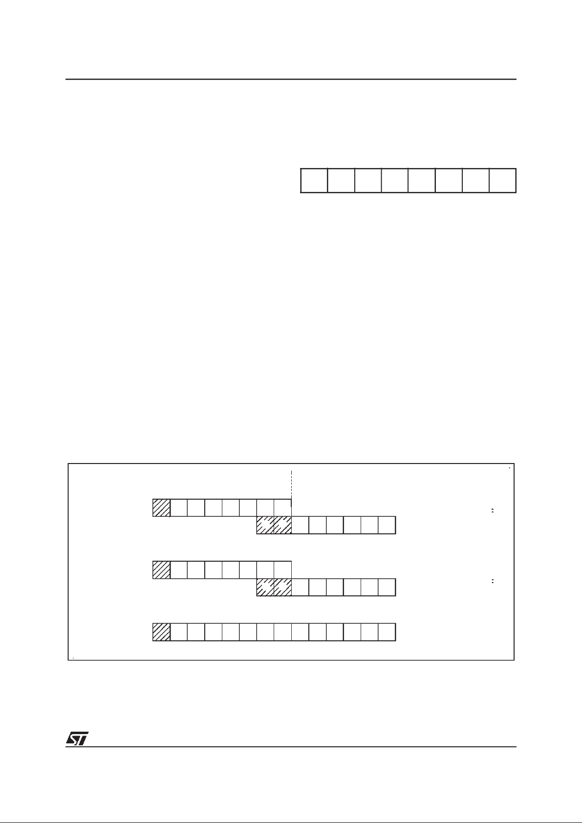
Figure 5. Data read-only memory Window Memory Addressing
543210
DATA ROM
WINDOW REGISTER
CONTENTS
(DWR)
12
13
765432 0
67891011
1
543210
01
Example:
DWR=28h
ROM
ADDRESS:A19h
11
00000000
11
0
0000
0
1
1
01001
1
11
PROGRAM SPACE ADDRESS
READ
DATA SPACE ADDRESS
40h-7Fh
IN INSTRUCTION
DATA SPACE ADDRESS
59h
VR0A1573
11/78
11
Page 12

ST62T80B/E80B
MEMORY MAP (Cont’d)
1.3.6 Data RAM/EEPROM and LCD RAM Bank
Register (DRBR)
Address: CBh — Write only
70
- DRBR6 DRBR5 DRBR4 DRBR3 - DRBR1 DRBR0
Bit 7 = This bit is not used
Bit 6 - DRBR6. This bit, when set, selects LCD
RAM Page 2.
Bit 5 - DRBR5. This bit, when set, selects LCD
RAM Page 1.
Bit 4 - DRBR4. This bit, when set, selects RAM
Page 2.
Bit 3 - DRBR3. This bit, when set, selects RAM
Page 1.
Bit2. These bits are not used.
Bit 1 - DRBR1. This bit, when set, selects
EEPROM Page 1.
Bit 0 - DRBR0. This bit, when set, selects
EEPROM Page 0.
The selection of the bank is made by programming
the Data RAM Bank Switch register (DRBR register) located at address CBh of the Data Space according to Table 1. No more than one bank should
be set at a time.
The DRBR register can be addressed like a RAM
Data Space at the address CBh; nevertheless it is
a write only register that cannot be accessed with
single-bit operations. This register isused to select
the desired 64-byte RAM/EEPROM bank of the
Data Space. Thenumber of banks has to be loaded in the DRBR register and the instruction has to
point to the selected location as if it was in bank 0
(from 00h address to 3Fh address).
This register is not cleared during the MCU initialization, therefore it must be written before the first
access to the Data Space bank region. Refer to
the Data Space description for additional information. The DRBR register is not modified when an
interrupt or a subroutine occurs.
Notes :
Care is required when handling the DRBR register
as it is write only. For this reason, it is not allowed
to change the DRBR contents while executing interrupt service routine, as the service routine cannot save and thenrestore its previous content. If it
is impossible to avoid the writing of this register in
interrupt service routine, an image of this register
must be saved in a RAM location, and each time
the program writes to DRBR it must write also to
the image register. The image register must be
written first, so if an interrupt occurs between the
two instructions the DRBR is not affected.
In DRBR Register, only 1 bit must be set. Otherwise two or more pages are enabled in parallel,
producing errors.
Table 5. Data RAM Bank Register Set-up
DRBR ST62T80B/E80B
00 None
01 EEPROM Page 0
02 EEPROM Page 1
08 RAM Page 1
10h RAM Page 2
20h LCD RAM Page 1
40h LCD RAM Page 2
other Reserved
12/78
12
Page 13

MEMORY MAP (Cont’d)
1.3.7 EEPROM Description
EEPROM memory is located in 64-byte pages in
data space. This memory maybe used by theuser
program for non-volatile data storage.
Data spacefrom 00h to3Fh is paged as described
in Table 6. EEPROM locations are accessed directly by addressing these paged sections of data
space.
The EEPROM does not require dedicated instructions forreadorwrite access.Onceselectedvia the
Data RAM Bank Register, the active EEPROM
page is controlled by the EEPROM Control Register (EECTL), which is described below.
Bit E20FFof the EECTL registermust bereset prior
to any write or read access to the EEPROM. If no
bank hasbeen selected, or if E2OFF is set, any access is meaningless.
Programming must be enabled by setting the
E2ENA bit of the EECTL register.
The E2BUSY bitof the EECTL register is setwhen
the EEPROM is performing a programming cycle.
Any access to the EEPROM when E2BUSY is set
is meaningless.
Provided E2OFF and E2BUSY are reset, an EEPROM location is read just like any other data location, also in terms of access time.
Writing to the EEPROM may be carried out in two
modes: Byte Mode (BMODE) and Parallel Mode
ST62T80B/E80B
(PMODE). In BMODE, one byte is accessed at a
time, while in PMODE up to 8 bytes in the same
row are programmed simultaneously (with consequent speed and power consumption advantages,
the latter being particularly important in battery
powered circuits).
General Notes:
Data should be written directly to the intended ad-
dress in EEPROM space. There is nobuffer memory between data RAM and the EEPROM space.
When the EEPROM is busy (E2BUSY = “1”)
EECTL cannot be accessed in write mode, it is
only possible to read the status of E2BUSY. This
implies that as long as the EEPROM is busy, it is
not possible to change the status of the EEPROM
Control Register. EECTL bits 4 and 5 are reserved
and must never be set.
Care is required whendealing withthe EECTL register, as some bits are write only. For this reason,
the EECTL contents must not be altered while executing an interrupt service routine.
If it is impossible to avoid writing to this register
within an interrupt service routine, an image of the
register must be saved in a RAM location, and
each time the program writes to EECTL it must
also write to the image register.The image register
must be written to first so that, if an interrupt occurs between the two instructions, the EECTL will
not be affected.
Table 6. Row Arrangement for Parallel Writing of EEPROM Locations
Dataspace
addresses.
Banks 0 and 1.
Byte 0 1234567
ROW7 38h-3Fh
ROW6 30h-37h
ROW5 28h-2Fh
ROW4 20h-27h
ROW3 18h-1Fh
ROW2 10h-17h
ROW1 08h-0Fh
ROW0 00h-07h
Up to 8 bytes in each row may be programmed simultaneously in Parallel Write mode.
The number of available 64-byte banks (1 or 2) is device dependent.
13/78
13
Page 14

ST62T80B/E80B
MEMORY MAP (Cont’d)
Additional Notes on Parallel Mode:
If the user wishes to perform parallel programming, the first step should be to set the E2PAR2
bit. From this time on, the EEPROM will be addressed in write mode, the ROW address will be
latched and it will be possible to change it only at
the end of the programming cycle, or by resetting
E2PAR2 without programming the EEPROM. After the ROW addressis latched,the MCU can only
“see” the selected EEPROM row and any attempt
to write or read other rows will produce errors.
The EEPROM should not be read while E2PAR2
is set.
As soon as the E2PAR2 bit is set, the 8 volatile
ROW latches are cleared. From this moment on,
the user can load data in allor in part ofthe ROW.
Setting E2PAR1 will modify the EEPROM registers corresponding to the ROW latches accessed
after E2PAR2. For example, if the software sets
E2PAR2 and accesses the EEPROM by writing to
addresses 18h, 1Ah and 1Bh, and then sets
E2PAR1, these three registers will be modified simultaneously; the remaining bytes in the row will
be unaffected.
Note that E2PAR2 is internally reset at the end of
the programming cycle. This implies that the user
must setthe E2PAR2 bit between two parallel programming cycles. Note that if the user tries to set
E2PAR1 while E2PAR2 is not set, there will be no
programming cycleand the E2PAR1 bit will be unaffected. Consequently, the E2PAR1bit cannot be
set if E2ENA is low. The E2PAR1 bit can be setby
the user, only if the E2ENA and E2PAR2 bits are
also set.
EEPROM Control Register (EECTL)
Address: DFh — Read/Write
Reset status: 00h
70
D7 E2OFF D5 D4 E2PAR1 E2PAR2 E2BUSY E2ENA
Bit 7 = D7:
Bit6= E2OFF:
Unused.
Stand-byEnable Bit.
WRITE ONLY.
IfthisbitissettheEEPROMisdisabled(anyaccess
will bemeaningless) and the power consumption of
the EEPROM is reduced to its lowest value.
Bit 5-4 = D5-D4:
Bit 3 = E2PAR1:
Reserved.
MUST be kept reset.
Parallel Start Bit.
WRITE ONLY.
OnceinParallelMode,as soonastheuser software
sets the E2PAR1 bit, parallel writing of the 8 adjacent registers will start. This bit is internally reset at
the end of the programming procedure. Note that
less than 8 bytescan bewritten if required, the undefined bytes being unaffected by the parallel programmingcycle;thisis explained ingreater detailin
the Additional Notes on Parallel Mode overleaf.
Bit 2 = E2PAR2:
Parallel Mode En. Bit.
WRITE
ONLY. This bit must be set by the user program in
order to perform parallel programming. If E2PAR2
is set and the parallel start bit (E2PAR1) is reset,
up to 8 adjacent bytes can be written simultaneously. These 8 adjacent bytes are considered as a
row, whose address lines A7, A6, A5, A4, A3 are
fixed while A2, A1 and A0 are the changingbits, as
illustrated in Table 6. E2PAR2 is automatically reset at the end of any parallel programming procedure. It can be reset by the user software before
starting the programming procedure, thus leaving
the EEPROM registers unchanged.
Bit 1 = E2BUSY:
EEPROM Busy Bit.
READ ONLY. This bit is automatically set by the EEPROM
control logic when the EEPROM is in programming mode. The userprogram should test it before
any EEPROM read or write operation; any attempt
to access the EEPROM while the busy bit is set
will be aborted and the writing procedure in
progress will be completed.
Bit 0 = E2ENA:
EEPROM Enable Bit.
WRITE ONLY. This bit enables programming of the EEPROM
cells. It must be set before any write to the EEPROM register. Any attempt to write to the EEPROM when E2ENA is low is meaningless and will
not trigger a write cycle.
14/78
14
Page 15

1.4 PROGRAMMING MODES
ST62T80B/E80B
1.4.1 Option Byte
The Option Byte allows configuration capability to
the MCUs. Option byte’s content is automatically
read, and the selected options enabled, when the
chip reset is activated.
It can only be accessed during the programming
mode. This access is made either automatically
(copy from a master device) or by selecting the
OPTION BYTE PROGRAMMING modeof the programmer.
The option byte is located in a non-user map. No
address has to be specified.
EPROM Code Option Byte
70
--
PRO-
TECT
NMI
PULL
- WDACT -
Bit 7-5. Reserved.
Bit 5= PROTECT. This bit allows the protection of
the software contents against piracy. When the bit
PROTECT is set high, readout of the OTP contents is prevented by hardware. No programming
equipment is able to gain access to the user program. When this bit is low, the user program can
be read.
Bit 4. Reserved.
Bit 3 = NMI PULL. . This bit must beset highto en-
able the internal pull-up resistor. When low, no
pull-up is provided.
Bit 2. Reserved.
Bit 1 = WDACT. This bit controls the watchdog ac-
tivation. When it is high, hardware activation is selected. The software activation is selected when
WDACT is low.
Bit 0 = Reserved.
The Option byte is written during programming ei-
ther by using the PC menu (PC driven Mode) or
1.4.2 Program Memory
EPROM/OTP programming mode is set by a
+12.5V voltage applied to the TEST/VPPpin. The
programming flow of the ST62T80B/E80B is described in the User Manual of the EPROM Programming Board.
The MCUs can be programmed with the
ST62E8xB EPROM programming tools available
from STMicroelectronics.
1.4.3 EEPROM Data Memory
EEPROM data pages are supplied in the virgin
state FFh. Partial or total programming of EEPROM data memory can be performed either
through the application software, or through anexternal programmer. Any STMicroelectronics tool
used for the program memory (OTP/EPROM) can
also be used to program the EEPROM data memory.
1.4.4 EPROM Erasing
The EPROM of the windowed package of the
MCUs may be erased by exposure to Ultra Violet
light. The erasure characteristic of the MCUs is
such that erasure begins when the memory is exposed to light with a wave lengths shorter than approximately 4000Å. It should be noted that sunlights and some types of fluorescent lamps have
wavelengths in the range 3000-4000Å.
It is thus recommended that the window of the
MCUs packages be covered by an opaque label to
prevent unintentional erasure problems when testing the application in such an environment.
The recommended erasure procedure of the
MCUs EPROM is the exposure to short wave ultraviolet light which have a wave-length 2537A.
The integrated dose (i.e. U.V. intensity x exposure
time) for erasure should be a minimum of 15Wsec/cm2. The erasure time with this dosage is approximately 15 to 20 minutes using an ultraviolet
lamp with 12000µW/cm2power rating. The
ST62E80B should be placed within 2.5cm (1Inch)
of the lamp tubes during erasure.
automatically (stand-alone mode)
15/78
15
Page 16
ST62T80B/E80B
2 CENTRAL PROCESSING UNIT
2.1 INTRODUCTION
The CPU Coreof ST6devicesisindependent ofthe
I/O or Memory configuration. As such, it may be
thought of as an independent central processor
communicating with on-chip I/O, Memory and Peripherals via internal address, data, and control
buses. In-core communication is arranged as
shown in Figure 6; the controller being externally
linked to both the Reset and Oscillator circuits,
while thecore is linked to thededicated on-chip peripherals via the serial data bus and indirectly, for
interrupt purposes, through the control registers.
2.2 CPU REGISTERS
TheST6FamilyCPUcorefeaturessixregisters and
three pairs of flags available to the programmer.
These are described in the following paragraphs.
Accumulator (A). The accumulator is an 8-bit
general purpose register used in all arithmetic calculations, logical operations, and data manipulations. The accumulator can be addressed in Data
space as a RAM location at address FFh. Thus the
ST6 can manipulate the accumulator just like any
other register in Data space.
Figure 6. ST6 Core Block Diagram
Indirect Registers (X, Y). These two indirect reg-
isters are used as pointers to memory locations in
Data space. They are used in the register-indirect
addressing mode. These registers can be addressed in the dataspace as RAM locations at addresses 80h (X) and 81h (Y). They can also beaccessed with the direct, short direct, or bit direct addressing modes. Accordingly, the ST6 instruction
set can usethe indirect registers as any other register of the data space.
Short Direct Registers (V, W). These two registers are used to save a byte in short direct addressing mode. They can be addressed in Data
space as RAM locations at addresses 82h (V)and
83h (W). They can also be accessed using the direct and bit direct addressing modes. Thus, the
ST6 instruction set can use the short direct registers as any other register of the data space.
Program Counter (PC). The program counter is a
12-bit register which contains the address of the
next ROM location to be processed by the core.
This ROM location may be an opcode, an operand, or the address of an operand. The 12-bit
length allows the direct addressing of 4096 bytes
in Program space.
PROGRAM
ROM/EPROM
12
RESET
CONTROLLER
OPCODE
Program Counter
and
6 LAYER STACK
FLAG
VALUES
0,01 TO 8MHz
OSCin
CONTROL
SIGNALS
2
A-DATA
FLAGS
OSCout
ADDRESS/READ LINE
ADDRESS
DECODER
B-DATA
ALU
RESULTS TO DATA SPACE (WRITE LINE)
INTERRUPTS
256
DATA SPACE
DATA
RAM/EEPROM
DATA
ROM/EPROM
DEDICATIONS
ACCUMULATOR
VR01811
16/78
16
Page 17

CPU REGISTERS (Cont’d)
However, ifthe program space contains more than
4096 bytes, the additional memory in program
space can be addressed by using the Program
Bank Switch register.
The PC value is incremented after reading the address of the current instruction. Toexecute relative
jumps, the PC and the offset are shifted through
the ALU, where they are added; the result is then
shifted backinto the PC.The programcounter can
be changedin the following ways:
- JP (Jump) instructionPC=Jump address
- CALL instructionPC= Call address
- Relative Branch Instruction.PC= PC +/- offset
- Interrupt PC=Interrupt vector
- Reset PC= Reset vector
- RET & RETI instructionsPC= Pop (stack)
- Normal instructionPC=PC + 1
Flags (C, Z). The ST6 CPU includes three pairs of
flags (Carry and Zero), each pair being associated
with one of the three normal modes of operation:
Normal mode, Interrupt mode and Non Maskable
Interrupt mode. Each pair consists of a CARRY
flag and a ZERO flag. One pair (CN, ZN) is used
during Normal operation, another pair is used during Interrupt mode (CI, ZI), and a third pair is used
in the Non Maskable Interrupt mode (CNMI, ZNMI).
The ST6 CPU uses the pair of flags associated
with the current mode: as soon as an interrupt (or
a Non Maskable Interrupt) is generated, the ST6
CPU uses the Interrupt flags (resp. the NMI flags)
instead of the Normal flags. When the RETI instruction is executed, the previously used set of
flags is restored. It should be noted that each flag
set can only be addressed in its own context (Non
Maskable Interrupt, Normal Interrupt or Main routine). The flags are not cleared during context
switching and thus retain their status.
The Carry flag is set when a carry or a borrow occurs during arithmetic operations; otherwise it is
cleared. The Carry flag is also set to the value of
the bit tested in a bit test instruction; it also participates in the rotate left instruction.
The Zero flag is set if the result of the last arithmetic or logical operation was equal to zero; otherwise it is cleared.
Switching between the three sets of flags is performed automatically when an NMI, an interrupt or
a RETI instructions occurs. As the NMI mode is
ST62T80B/E80B
automatically selected after the reset of the MCU,
the ST6 core uses at first the NMI flags.
Stack. The ST6 CPU includes a true LIFO hardware stack which eliminates the need for a stack
pointer. The stack consists of six separate 12-bit
RAM locations that do not belong to the data
space RAM area. When a subroutine call (or interrupt request) occurs, the contents of each level are
shifted intothe next higher level, while the content
of the PC is shifted into the first level (the original
contents of the sixth stack level are lost). When a
subroutine or interruptreturn occurs (RET or RETI
instructions), the first level register is shifted back
into the PC and the value of each level is popped
back into the previous level. Since the accumulator, in common with all other data space registers,
is not stored in this stack, management of these
registers should be performed within the subroutine. The stack will remain in its “deepest” position
if morethan 6 nested calls orinterrupts are executed, and consequently the last return address will
be lost. It will also remain in its highest position if
the stack is emptyand aRET or RETI is executed.
In this case the next instruction will be executed.
Figure 7. ST6 CPU Programming Mode
l
INDEX
REGISTER
INTERRUPTFLAGS
NMI FLAGS
b7
b7
b7
b7
b7
PROGRAMCOUNTER
SIX LEVELS
STACKREGISTER
X REG. POINTER
Y REG. POINTER
VREGISTER
W REGISTER
ACCUM ULATOR
b0
b0
b0
b0
b0
b0b11
CZNORMAL FLAGS
CZ
CZ
SHORT
DIRECT
ADDRESSING
MODE
VA000 4 23
17/78
17
Page 18
ST62T80B/E80B
3 CLOCKS, RESET, INTERRUPTS AND POWER SAVING MODES
3.1 CLOCK SYSTEM
3.1.1 Main Oscillator
The MCU featuresa Main Oscillator which can be
driven by an external clock, or used in conjunction
with an AT-cut parallel resonant crystal or a suitable ceramic resonator.
Figure 8 illustrates various possible oscillator configurations using anexternal crystal or ceramic resonator, an external clock input. CL1an CL2should
have acapacitance in the range 12 to 22 pF for an
oscillator frequency in the 4-8 MHz range.
The internal MCU clock Frequency (F
) is divid-
INT
ed by 13 to drive the CPU core and by 12 to drive
the A/D converter and the watchdog timer, while
clock used to drive on-chip peripherals depends
on the peripheral as shown in the clock circuit
block diagram.
With an 8MHz oscillator frequency, the fastest machine cycle is therefore 1.625µs.
A machine cycle is the smallest unit of time needed
to executeany operation (for instance, toincrement
the Program Counter). An instruction may require
two, four, or five machine cycles for execution.
Figure 9. Clock Circuit Block Diagram
Figure 8. Oscillator Configurations
CRYSTAL/RESONATOR CLOCK
ST6xxx
OSC
C
L1n
EXTERNAL CLOCK
OSC
in
ST6xxx
in
OSC
OSC
NC
out
out
C
L2
VA0016
VA0015A
OSCin
OSCout
OSC32in
OSC32out
18/78
18
f
OSC
MAIN
OSCILLATOR
32kHz
OSCILLATOR
POR
f
INT
f
INT
MUX
EOCR bit 5
(START/STOP)
:13
:12
Core
Timer 1 & 2
Watchdog
ADC
LCD
CONTROLLER
DRIVER
Page 19

CLOCK SYSTEM (Cont’d)
3.1.2 32 KHz STAND-BY OSCILLATOR
An additional32KHz stand-by on chip oscillatorallows to generate real time interrupts and to supply
the clock to the LCD driver with the main oscillator
stopped. This enables the MCU to perform real
time functions with the LCD display running while
keeping advantages of low power consumption.
Figure 10 shows the 32KHz oscillator block diagram.
A 32.768KHz quartz crystalmust be connected to
the OSC32in and OSC32out pins to perform the
real time clock operation. Two external capacitors
of 15-22pF each must be connected between the
oscillator pinsand ground. The 32KHz oscillator is
managed by the dedicated status/control register
32OCR.
As long as the 32KHz stand-by oscillator is enabled, 32KHz internal clock is available to drive
LCD controller driver. This clock is divide by 214to
generate interrupt request every 500ms . The periodic interrupt request serves as reference timebase for real time functions.
Note: When the 32KHz stand-by oscillator is
stopped (bit 5 of the Status/Control register
cleared) the divider chain is supplied with a clock
signal synchronous with machine cycle (f
this produces an interrupt request every 13x2
INT
/13),
14
clock cycle (i.e. 26.624ms) with an 8MHz quartz
crystal.
ST62T80B/E80B
32KHz Oscillator Register (32OCR)
Address: DBh - Read/Write
70
EOSCI OSCEOC S/S D4 D3 D2 D1 D0
Bit 7= EOSCI.
when set, enables the 32KHz oscillator interrupt
request.
Bit 6 = OSCEOC.
indicates whenthe 32KHzoscillator has measured
a 500ms elapsed time (providing a
32.768KHzquartz crystal is connected to the
32KHz oscillator dedicated pins). An interrupt request can be generated in relation to the state of
EOSCI bit. This bit must be cleared by the user
program before leaving the interrupt service routine.
Bit 5 = START/STOP.O
This bit, when set, enables the 32KHz stand-by
oscillator and the free running divider chainis supplied by the 32KHz oscillator signal. When this bit
is cleared to zero the divider chain is supplied with
f
/13.
INT
This register is cleared during reset.
Note:
To achieve minimumpower consumption in STOP
mode (no system clock), the stand-by oscillator
must be switched off (real time function not available) by clearing the Start/Stop bit in the oscillator
status/control register.
Enable Oscillator Interrupt
Oscillator Interrupt Flag
scillator Start/Stop bit
. This bit,
. This bit
.
Figure 10. 32KHz Oscillator Block Diagram
2x15...22pF
OSC32IN
OSC32KHz MUX
32.768KHz
Crystal
OSC32OUT
EOSCI OSCEOC
START
STOP
OSC32KHz
f
INT
INT
1
0
/13
XXXXX
DIV2
14
19/78
19
Page 20
ST62T80B/E80B
3.2 RESETS
The MCU can be reset in three ways:
– by the external Reset input being pulled low;
– by Power-on Reset;
– by the digital Watchdog peripheral timing out.
3.2.1 RESET Input
The RESET pin may be connected to a device of
the application board in order to reset the MCU if
required. The RESET pin may be pulled low in
RUN, WAIT or STOP mode. This input can be
used to reset the MCU internal state and ensure a
correct start-up procedure. The pin is active low
and features a Schmitt trigger input. The internal
Reset signal is generated by adding a delay to the
external signal. Therefore even short pulses on
the RESET pin are acceptable, provided VDDhas
completed its risingphase andthat the oscillator is
running correctly (normal RUN or WAIT modes).
The MCU is kept in the Reset state as long as the
RESET pin is held low.
If RESET activation occurs in the RUN or WAIT
modes, processing of the user program is stopped
(RUN modeonly), the Inputs and Outputs are configured as inputs with pull-up resistors and the
main Oscillator is restarted. When the level on the
RESET pin then goes high, the initialization sequence is executed following expiry of the internal
delay period.
If RESET pin activation occurs in the STOP mode,
the oscillator starts up and all Inputs and Outputs
are configured as inputs with pull-up resistors.
When the level of the RESET pin then goes high,
the initialization sequence is executed following
expiry of the internal delay period.
3.2.2 Power-on Reset
The function of the POR circuit consists in waking
up the MCU at an appropriate stage during the
power-on sequence. At the beginning of this sequence, the MCU is configured in the Reset state:
all I/O ports are configured as inputs with pull-up
resistors and no instruction is executed. When the
power supplyvoltage rises to a sufficient level, the
oscillator starts to operate, whereupon an internal
delay is initiated, in order to allow the oscillator to
fully stabilize before executing the first instruction.
The initialization sequence isexecuted immediately following the internal delay.
The internaldelay isgenerated byan on-chipcounter. Theinternal reset lineis released 2048 internal
clock cycles after release of the external reset.
Notes:
To ensure correct start-up, the user should take
care that the reset signal is not released before the
VDDlevel is sufficient to allow MCU operation at
the chosen frequency (see Recommended Operating Conditions).
A proper reset signal for a slow rising VDDsupply
can generally be provided by an external RC network connected to the RESET pin.
Figure 11. Reset and Interrupt Processing
RESET
NMI MASK SET
INT LATCH CLEARED
( IF PRESENT )
SELECT
NMI MODE FLAGS
PUT FFEH
ON ADDRESS BUS
YES
IS RESET STILL
PRESENT?
NO
LOAD PC
FROM RESET LOCATIONS
FFE/FFF
FETCH INSTRUCTION
VA000427
20/78
20
Page 21

RESETS (Cont’d)
3.2.3 Watchdog Reset
The MCU provides a Watchdog timer function in
order to ensure graceful recovery from software
upsets. If the Watchdog register is not refreshed
before an end-of-count condition is reached, the
internal reset will be activated. This, amongst other things, resets the watchdog counter.
The MCU restarts just as though the Reset had
been generated by the RESET pin, including the
built-in stabilisation delay period.
3.2.4 Application Notes
No external resistor is required between VDDand
the Reset pin, thanks to the built-in pull-up device.
The POR circuit operates dynamically, in that it
triggers MCU initialization on detecting the rising
edge of VDD. The typical threshold is in the region
of 2 volts, but the actual value of the detected
threshold depends on the way in which VDDrises.
The POR circuit is
NOT
designed to supervise
static, or slowly rising or falling VDD.
3.2.5 MCU Initialization Sequence
When a reset occurs the stack is reset, the PC is
loaded with the address of the Reset Vector (located in program ROM starting at address 0FFEh). A
jump tothe beginning of theuser program must be
coded at this address. Following a Reset, the Interrupt flag is automatically set, so that the CPU is
in Non Maskable Interrupt mode; this prevents the
ST62T80B/E80B
initialisation routine from being interrupted. The initialisation routine should therefore be terminated
by a RETI instruction, in order to revert to normal
mode and enable interrupts. Ifno pending interrupt
is presentat theend of the initialisation routine, the
MCU will continue by processing the instruction
immediately following the RETI instruction. If, however, a pending interrupt is present, it will be serviced.
Figure 12. Reset and Interrupt Processing
RESET
JP:2 BYTES/4 CYCLES
RESET
VECTOR
INITIALIZATION
ROUTINE
JP
RETI: 1 BYTE/2 CYCLES
RETI
VA00181
Figure 13. Reset Block Diagram
V
DD
300kΩ
RESET
2.8kΩ
POWER
WATCHDOG RESET
ON RESET
f
OSC
RESET
CK
COUNTER
RESET
ST6
INTERNAL
RESET
VA0200B
21/78
21
Page 22

ST62T80B/E80B
RESETS (Cont’d)
Table 7. Register Reset Status
Register Address(es) Status Comment
EEPROM Control Register
Port Data Registers
Port A,B Direction Register
Port A,B Option Register
Interrupt Option Register
0DFh
0C0h, 0C1h, 0C3h
0C4h to 0C6h
0CCh, 0CEh, OCFh
0C8h
00h
EEPROM enabled
I/O are Input with pull-up
Interrupt disabled
SPI Registers
LCD Mode Control Register
32kHz Oscillator Register
UART Control
UART Data Register
X, Y,V, W, Register
Accumulator
Data RAM
Data RAM/EEPROM/LCDRAM Page Register
Data ROM Window Register
EEPROM
A/D Result Register
TIMER 1 Status/Control
TIMER 1 Counter Register
TIMER 1 Prescaler Register
Watchdog Counter Register
A/D Control Register
AR TIMER Mode Control Register
AR TIMER Status/Control 1 Register
AR TIMER Status/Control 2Register
AR TIMER Compare Register
0C2h, 0DDh
0DCh
0DBh
080H TO 083H
0FFh
084h to 0BFh
0CBh
0C9h
00h to 03Fh
0D0h
0D4h
0D3h
0D2h
0D8h
0D1h
0E5h
0E6h
0E7h
0EAh
SPI disabled
LCD display off
Interrupt disabled
00h UART disabled
Undefined As written if programmed
00h
FFh
7Fh
FEh
40h
00h
TIMER 1 disabled/Max count
loaded
A/D in Standby
AR TIMER stopped
AR TIMER Load Register
AR TIMER Reload/Capture Register
22/78
22
0EBh
0E9h
Undefined
As written if programmed
Page 23

3.3 DIGITAL WATCHDOG
ST62T80B/E80B
The digital Watchdog consists of a reloadable
downcounter timer which can be used to provide
controlled recovery from software upsets.
The Watchdog circuit generates a Reset when the
downcounter reaches zero. User software can
prevent this reset by reloading the counter, and
should therefore be written so that the counter is
regularly reloaded while the user program runs
correctly. Inthe event of a software mishap (usually caused by externally generated interference),
the userprogram will no longer behave in its usual
fashion and the timer register will thus not be reloaded periodically. Consequently the timer will
decrement down to 00h and reset the MCU. In order to maximise the effectiveness of the Watchdog
function, user software must be written with this
concept in mind.
Table 8. Recommended Option Choices
Functions Required Recommended Options
Stop Mode “SOFTWARE WATCHDOG”
Watchdog “HARDWARE WATCHDOG”
Watchdog behaviour is governed by one option,
known as “WATCHDOG ACTIVATION” (i.e.
HARDWARE or SOFTWARE) (See Table8).
In the SOFTWARE option, the Watchdog is disabled until bit C of the DWDR register has been set.
When the Watchdog is disabled, low power Stop
mode is available. Once activated, the Watchdog
cannot be disabled, except by resetting the MCU.
In the HARDWARE option, the Watchdog is permanently enabled. Sincethe oscillatorwill run continuously, low power mode is not available. The
STOP instruction is interpreted as a WAIT instruction, and the Watchdog continues to countdown.
When the MCU exits STOP mode (i.e. when aninterrupt is generated), the Watchdog resumes its
activity.
23/78
23
Page 24

ST62T80B/E80B
DIGITAL WATCHDOG (Cont’d)
The Watchdog is associated with a Data space
register (Digital WatchDog Register, DWDR, location 0D8h) which is described in greater detail in
Section 3.3.1 . This register is set to 0FEh on Reset: bit C is cleared to “0”, which disables the
Watchdog; the timer downcounter bits, T0 to T5,
and the SR bit are all set to “1”, thus selecting the
longest Watchdog timer period. This time period
can be set to the user’s requirements by setting
the appropriate value for bits T0 to T5 in the
DWDR register. The SR bit must be set to “1”,
since itis this bit which generates the Reset signal
when it changes to “0”; clearing this bit would generate an immediate Reset.
It should be noted that the order of the bits in the
DWDR register is inverted with respect to the associated bits in the down counter: bit 7 of the
DWDR register corresponds, in fact, to T0 and bit
2 to T5. The user should bear in mind the fact that
these bits are inverted and shifted with respect to
the physicalcounter bits when writing tothis register. The relationship between the DWDR register
bits and the physical implementation ofthe Watchdog timer downcounter is illustrated in Figure 14.
Only the 6 most significant bits may be used to define the time period, since it is bit 6 which triggers
the Reset when it changes to “0”. This offers the
user a choice of 64 timed periods ranging from
3,072 to 196,608 clock cycles (with an oscillator
frequency of8MHz, this is equivalent to timer periods ranging from 384µs to 24.576ms).
Figure 14. Watchdog Counter Control
D0
D1
C
SR
RESET
D2
D3
D4
D5
D6
WATCHDOG CONTROL REGISTER
D7
T5
T4
T3
WATCHDOG COUNTER
T2
T1
T0
8
÷2
OSC÷12
VR02068A
24/78
24
Page 25

DIGITAL WATCHDOG (Cont’d)
3.3.1 Digital Watchdog Register (DWDR)
Address: 0D8h — Read/Write
Reset status: 1111 1110b
70
It should be noted that the register bits are reversed and shifted with respect to the physical
counter: bit-7 (T0) is the LSB of the Watchdog
downcounter and bit-2 (T5) is the MSB.
These bits are set to “1” on Reset.
ST62T80B/E80B
T0 T1 T2 T3 T4 T5 SR C
Bit 0 = C:
Watchdog Control bit
If the hardware option is selected, this bitis forced
high and the user cannot change it (the Watchdog
is always active). When the software option is selected, the Watchdog function is activated by setting bit C to 1, and cannot then be disabled (save
by resetting the MCU).
When C is kept low the counter can be used as a
7-bit timer.
This bit is cleared to “0” on Reset.
Bit 1 = SR:
Software Reset bit
This bit triggers a Resetwhen cleared.
When C = “0” (Watchdog disabled) it is the MSB of
the 7-bit timer.
This bit is set to “1” on Reset.
Bits 2-7 = T5-T0:
Downcounter bits
3.3.2 Application Notes
The Watchdog plays an important supporting role
in the high noise immunity of ST62xx devices, and
should be used wherever possible. Watchdog related options should be selected on the basis of a
trade-off between application security and STOP
mode availability.
When STOP mode is not required, hardware activation should be preferred, as it provides maximum security, especially during power-on.
When software activation is selected and the
Watchdog is not activated, the downcounter may
be used as a simple 7-bit timer (remember that the
bits are in reverse order).
The software activation option should be chosen
only when the Watchdog counter is to be used as
a timer. To ensure the Watchdog has not been unexpectedly activated, the following instructions
should be executed within the first 27 instructions:
jrr 0, WD, #+3
25/78
25
Page 26

ST62T80B/E80B
DIGITAL WATCHDOG (Cont’d)
These instructions test the C bit and Reset the
MCU (i.e. disable the Watchdog) if the bit is set
(i.e. if the Watchdog is active), thus disabling the
Watchdog.
In all modes, a minimum of 28 instructions are executed after activation, before the Watchdog can
generate a Reset. Consequently, user software
Figure 15. Digital Watchdog Block Diagram
RESET
should load the watchdog counter within the first
27 instructions following Watchdog activation
(software mode), or within the first 27 instructions
executed following a Reset (hardware activation).
It should benoted that when the GEN bit is low(interrupts disabled), the NMI interrupt is active but
cannot cause a wake up from STOP/WAIT modes.
S
Q
RSFF
7
-2
R
DB0
DB1.7 SETLOAD
8
WRITE
RESET
DATA BUS
-2
SET
8
-12
OSCILLATOR
CLOCK
VA00010
26/78
26
Page 27

3.4 INTERRUPTS
ST62T80B/E80B
The CPU can manage four Maskable Interrupt
sources, in addition to a Non Maskable Interrupt
source (top priority interrupt). Each source is associated with a specific Interrupt Vector which contains aJump instruction to the associated interrupt
service routine. These vectors are located in Program space (see Table 9).
When an interrupt source generates an interrupt
request, and interrupt processing is enabled, the
PC registeris loaded with the address of the interrupt vector (i.e. of the Jump instruction), which
then causes a Jump to the relevant interrupt service routine, thus servicing the interrupt.
Interrupt sourcesare linked to events either on external pins, or on chip peripherals. Several events
can be ORed on the same interrupt source, and
relevant flags are available to determine which
event triggered the interrupt.
The Non Maskable Interrupt request has the highest priority and can interrupt any interrupt routine
at any time; the other four interrupts cannot interrupt each other. If more than one interrupt request
is pending, these are processed by the processor
core according to theirpriority level: source #1 has
the higher priority while source #4 the lower. The
priority of each interrupt source is fixed.
Table 9. Interrupt Vector Map
Interrupt Source Priority Vector Address
Interrupt source #0 1 (FFCh-FFDh)
Interrupt source #1 2 (FF6h-FF7h)
Interrupt source #2 3 (FF4h-FF5h)
Interrupt source #3 4 (FF2h-FF3h)
Interrupt source #4 5 (FF0h-FF1h)
3.4.1 Interrupt request
All interrupt sources but the Non Maskable Interrupt source can be disabled by setting accordingly
the GEN bit of the Interrupt Option Register (IOR).
This GEN bitalso defines if aninterrupt source,including the Non Maskable Interrupt source, can restart the MCU from STOP/WAIT modes.
Interrupt request from the Non Maskable Interrupt
source #0 is latched by a flip flop which is automat-
ically resetby the core at the beginning of the nonmaskable interrupt service routine.
Interrupt request from source #1 can be configured either as edge or level sensitive by setting accordingly the LES bit of the Interrupt Option Register (IOR).
Interrupt request from source #2 are always edge
sensitive. The edge polarity can be configured by
setting accordingly the ESB bit of the Interrupt Option Register (IOR).
Interrupt request from sources #3 & #4 are level
sensitive.
In edge sensitive mode, alatch is set when a edge
occurs on the interrupt source line and is cleared
when the associated interrupt routine is started.
So, the occurrence of an interrupt can be stored,
until completion of the running interrupt routine before being processed. If several interruptrequests
occurs before completion of the running interrupt
routine, only the first request is stored.
Storage of interrupt requests is notavailable in level sensitive mode. To be taken into account, the
low level must bepresent onthe interrupt pin when
the MCU samples the line after instruction execution.
At the end of every instruction, the MCU tests the
interrupt lines: if there is an interrupt request the
next instruction is not executed and the appropriate interrupt service routine is executed instead.
Table 10. Interrupt Option Register Description
GEN
ESB
LES
OTHERS NOT USED
SET Enable all interrupts
CLEARED Disable all interrupts
SET
CLEARED
SET
CLEARED
Rising edge mode on interrupt source #2
Falling edge mode on interrupt source #2
Level-sensitive mode on interrupt source #1
Falling edge mode on interrupt source #1
27/78
27
Page 28

ST62T80B/E80B
INTERRUPTS (Cont’d)
3.4.2 Interrupt Procedure
The interrupt procedure is very similarto a callprocedure, indeed the user can consider the interrupt
as an asynchronous call procedure. As this is an
asynchronous event, the user cannot know the
context and the time at which it occurred. As a result, the user should save all Data space registers
which may be used within the interrupt routines.
There are separate sets of processor flags for normal, interrupt and non-maskable interrupt modes,
which are automatically switched and so do not
need to be saved.
The following list summarizes the interrupt procedure:
MCU
– The interrupt is detected.
– The C and Z flags are replaced by the interrupt
flags (or by the NMI flags).
– The PC contents are stored in the first level of
the stack.
– The normal interrupt lines are inhibited (NMI still
active).
– The first internal latch is cleared.
– TheassociatedinterruptvectorisloadedinthePC.
WARNING: In some circumstances, when a
maskable interrupt occurs while the ST6 core is in
NORMAL mode and especially during the execution of an ”ldi IOR, 00h” instruction (disabling all
maskable interrupts):if the interrupt arrives during
the first 3 cycles of the ”ldi” instruction (which is a
4-cycle instruction) the core will switch to interrupt
mode BUT the flags CN and ZN will NOT switch to
the interrupt pair CI and ZI.
User
– User selected registers are saved within the in-
terrupt service routine (normally on a software
stack).
– Thesource ofthe interrupt is found bypolling the
interrupt flags (if more than one source isassoci-
ated with the same vector).
– The interrupt is serviced.
– Return from interrupt (RETI)
MCU
– Automatically theMCU switches back to the nor-
mal flag set (or the interrupt flag set) and pops
the previous PC value from the stack.
The interrupt routine usually begins by the identifying the device which generated the interrupt request (by polling). The user should save the registers which are usedwithin the interrupt routine in a
software stack. After the RETI instruction is executed, the MCU returns to the main routine.
Figure 16. Interrupt Processing Flow Chart
INSTRU CTION
FETCH
INSTRU CTION
EXECUT E
INSTRUCTION
LOAD PC FROM
INTERR UPT VECTOR
(FFC/FFD)
SET
INTERRUPT MASK
PUSH THE
PC INTO THE STACK
SELECT
INTER NALMODE FLAG
VA000014
THE INSTRUCTION
YES
INTERR UPT MASK
PROGRAM FLAGS
THE STACKED PC
NO
WAS
ARETI
?
CLEAR
SELECT
”POP”
?
NO
?
YES
IS THE CORE
ALREADY IN
NORMAL MODE?
NO
CHEC K IF THERE IS
AN INTER RUPT REQUEST
AND INTE RRUPTMASK
YES
28/78
28
Page 29

INTERRUPTS (Cont’d)
3.4.3 Interrupt Option Register (IOR)
The Interrupt Option Register (IOR) is used to enable/disable theindividual interrupt sources and to
select the operating mode of the external interrupt
inputs. This register is write-only and cannot be
accessed by single-bit operations.
Address: 0C8h — Write Only
Reset status: 00h
70
- LES ESB GEN - - - -
Bit 5 = ESB:
Edge Selection bit
The bit ESB selects the polarity of the interrupt
source #2.
Bit 4= GEN:
Global Enable Interrupt
is set to one, all interrupts are enabled. When this
bit is cleared to zero all the interrupts (excluding
NMI) are disabled.
When the GEN bit is low, the NMI interrupt is active but cannot causea wake up from STOP/WAIT
modes.
This register is cleared on reset.
3.4.4 Interrupt sources
ST62T80B/E80B
.
. When thisbit
Bit 7, Bits 3-0 =
Bit 6 = LES:
Unused
.
Level/Edge Selection bit
.
When this bit is set to one, the interrupt source #1
Interrupt sources available on the
ST62E80B/T80B are summarized in the Table 11
with associated mask bit to enable/disable the in-
terrupt request.
is level sensitive. When cleared to zero the edge
sensitive mode for interrupt request is selected.
Table 11. Interrupt Requests and Mask Bits
Peripheral Register
GENERAL IOR C8h GEN
TIMER 1 TSCR1 D4h ETI TMZ: TIMER Overflow source 3
A/D CONVERTER ADCR D1h EAI EOC: End of Conversion source 4
SPI SPI C2h ALL End of Transmission source 1
Port PAn ORPA-DRPA C0h-C4h ORPAn-DRPAn PAnpin source 2
Port PBn ORPB-DRPB C1h-C5h ORPBn-DRPBn PBn pin source 2
Port PCn ORPC-DRPC C6h-CFh ORPCn-DRPCn PCn pin source 2
32kHz OSC 32OCR DBh EOSCI OSCEOC source 3
ARTIMER ARMC E5h
UART UARTCR D7h
Address
Register
Mask bit Masked Interrupt Source
All Interrupts, excluding NMI All
OVIE
CPIE
EIE
RXIEN
TXIEN
OVF: ARTIMER Overflow
CPF: Successful Compare
EF: Active edge on ARTIMin
RXRDY:byte received
TXMT: byte sent
Interrupt
source
source 3
source 4
29/78
29
Page 30

ST62T80B/E80B
INTERRUPTS (Cont’d)
Figure 17. Interrupt Block Diagram
NMI
PORT A
PORT B
PORT C
Bits
SPI
FROM REGISTER PORT A,B,C
SINGLE BIT ENABLE
PBE
V
DD
PBE
PBE
TIMER1
ARTIMER
OSC32kHz
OSCEOC
EOSCI
IOR bit 5 (ESB)
TMZ
ETI
OVF
OVIE
CPF
CPIE
EF
EIE
CLK Q
FF
CLK Q
CLR
FF
CLR
I
0
MUX
Start
I
1
1
IOR bit 6 (LES)
FF
CLK Q
CLR
0
I
2
INT #0 NMI (FFC,D))
Start
INT #1 (FF6,7)
RESTART
FROM
STOP/WAIT
INT #2 (FF4,5)
Start
INT #3 (FF2,3)
30/78
30
A/D CONVERTER
RXRDY
RXIEN
TXMT
TXIEN
EAI
EOC
INT #4 (FF0,1)
IOR bit 4(GEN)
Page 31

3.5 POWER SAVING MODES
ST62T80B/E80B
The WAIT and STOP modes have been implemented in the ST62xx family of MCUs in order to
reduce the product’s electrical consumption during
idle periods. These two power saving modes are
described in the following paragraphs.
3.5.1 WAIT Mode
The MCU goes into WAIT mode as soon as the
WAIT instruction is executed. The microcontroller
can be considered as being in a “software frozen”
state where the core stops processing the program instructions, the RAM contents and peripheral registers are preserved as long as the power
supply voltage is higher than the RAM retention
voltage. In this mode the peripherals are still active.
WAIT mode can be used when the user wants to
reduce the MCU power consumption during idle
periods, while not losing track of time or the capability of monitoring external events. The active oscillator is not stopped in order to provide a clock
signal to the peripherals. Timer counting may be
enabled as well as the Timer interrupt, before entering the WAIT mode: this allows the WAIT mode
to be exited when a Timer interrupt occurs. The
same applies to other peripherals which use the
clock signal.
If the WAIT mode is exited due to a Reset (either
by activating the external pin or generated by the
Watchdog), theMCU enters a normal reset procedure. If an interrupt is generated during WAIT
mode, the MCU’s behaviour depends on the state
of the processor coreprior to the WAIT instruction,
but also on the kind of interrupt request which is
generated. This is described in the following para-
graphs. The processor core does not generate a
delay following the occurrence of the interrupt, be-
cause the oscillator clock is still available and no
stabilisation period is necessary.
3.5.2 STOP Mode
If the Watchdog is disabled, STOP mode is availa-
ble. When in STOP mode, the MCU is placed in
the lowest power consumption mode. In this oper-
ating mode, the microcontroller can be considered
as being “frozen”, no instruction is executed, the
oscillator is stopped, the RAM contents and pe-
ripheral registers are preserved as long as the
power supply voltage is higher than the RAM re-
tention voltage, and the ST62xx core waits for the
occurrence of an external interrupt request or a
Reset to exit the STOP state.
If the STOP state is exited dueto a Reset (by acti-
vating the external pin) the MCU will enter a nor-
mal reset procedure. Behaviour in response to in-
terrupts depends on the state of the processor
core prior to issuing the STOP instruction, and
also on the kind of interrupt request that is gener-
ated.
This case will be described in the following para-
graphs. The processor core generates a delay af-
ter occurrence of the interrupt request, in order to
wait for complete stabilisation of the oscillator, be-
fore executing the first instruction.
31/78
31
Page 32

ST62T80B/E80B
POWER SAVING MODE (Cont’d)
3.5.3 Exit from WAIT and STOP Modes
The following paragraphs describe how the MCU
exits from WAIT and STOP modes, when an interrupt occurs (not a Reset). It should be noted that
the restart sequence depends on theoriginal state
of the MCU (normal, interrupt or non-maskable interrupt mode) prior to entering WAIT or STOP
mode, as well as on the interrupttype.
Interrupts do not affect the oscillator selection.
3.5.3.1 Normal Mode
If the MCUwas in themain routine when the WAIT
or STOP instruction was executed, exit from Stop
or Waitmode will occuras soon as an interrupt occurs; the related interrupt routine is executed and,
on completion, the instruction which follows the
STOP or WAIT instruction is then executed, providing no other interrupts are pending.
3.5.3.2 Non Maskable Interrupt Mode
If the STOP or WAIT instruction has been executed during execution of the non-maskable interrupt
routine, theMCU exits from the Stop or Wait mode
as soon as an interrupt occurs: the instruction
which follows the STOP or WAIT instruction is executed, and the MCU remains in non-maskable interrupt mode, even if another interrupt has been
generated.
3.5.3.3 Normal Interrupt Mode
If theMCU was in interrupt mode before the STOP
or WAIT instruction was executed, it exits from
STOP or WAIT mode as soon as an interrupt occurs. Nevertheless, two cases must be considered:
– If the interrupt is a normal one, the interrupt rou-
tine in which the WAIT or STOP mode was en-
tered will be completed, starting with the
execution of the instruction which follows the
STOP or the WAIT instruction, and the MCU is
still in the interrupt mode. At the end of this routine pendinginterrupts will be serviced in accordance with their priority.
– In the event of a non-maskable interrupt, the
non-maskable interrupt service routine is processed first, then the routine in which the WAIT or
STOP mode was entered will be completed by
executing the instruction following the STOP or
WAIT instruction. The MCU remains in normal
interrupt mode.
Notes:
To achieve the lowest power consumption during
RUN or WAIT modes, the user program must take
care of:
– configuringunused I/Os as inputs without pull-up
(these should be externally tied to well defined
logic levels);
– placing all peripherals in their power down
modes before entering STOP mode;
When the hardware activated Watchdog is select-
ed, or whenthe software Watchdogis enabled, the
STOP instruction is disabled and a WAIT instruc-
tion will be executed in its place.
If all interrupt sources are disabled (GEN low), the
MCU can only be restarted by a Reset. Although
setting GEN low does not mask the NMI as an in-
terrupt, it will stop it generating a wake-up signal.
The WAIT and STOP instructions are not execut-
ed if an enabled interrupt request is pending.
32/78
32
Page 33

4 ON-CHIP PERIPHERALS
4.1 I/O PORTS
ST62T80B/E80B
The MCU features Input/Output lines which may
be individually programmed as any of the following
input or output configurations:
– Input withoutpull-up or interrupt
– Input with pull-up and interrupt
– Input with pull-up, but without interrupt
– Analog input
– Push-pull output
– Open drain output
The lines are organised as bytewise Ports.
Each port is associated with 3 registers in Data
space. Each bit of these registers is associated
with a particular line (for instance, bits 0 of Port A
Data, Direction and Option registers are associated with the PA0 line of Port A).
The DATA registers (DRx), are used to read the
voltage level values of the lines which have been
configured as inputs, or to write the logic value of
the signal to be output on the lines configured as
outputs. Theport data registers can be readto get
the effective logic levels of the pins, but they can
Figure 18. I/O Port Block Diagram
S
CONTROLS
IN
RESET
be also written by user software, in conjunction
with the related option registers, to select the dif-
ferent input mode options.
Single-bit operations on I/O registers are possible
but care is necessary because reading in input
mode is done from I/O pins while writing will direct-
ly affect the Port data register causing an unde-
sired change of the input configuration.
The Data Direction registers (DDRx) allow the
data direction (input or output) of each pin to be
set.
The Option registers (ORx) are used to select the
different port options available both in input and in
output mode.
All I/O registers can be read or written to just as
any other RAM location in Data space, so no extra
RAM cells are needed for port data storage and
manipulation. During MCU initialization, all I/Oreg-
isters are cleared andthe input mode with pull-ups
and no interrupt generation is selected for all the
pins, thus avoiding pin conflicts.
V
DD
SHIFT
REGISTER
S
OUT
TO INTERRUPT
TO ADC
DATA
DIRECTION
REGISTER
DATA
REGISTER
OPTION
REGISTER
V
DD
INPUT/OUTPUT
VA00413
33/78
33
Page 34

ST62T80B/E80B
I/O PORTS (Cont’d)
4.1.1 Operating Modes
Each pinmay be individually programmed asinput
or output with various configurations.
This is achieved by writing the relevant bit in the
Data (DR), Data Direction (DDR) and Option registers (OR). Table 12 illustrates the various port
configurations which can be selected by user software.
4.1.1.1 Input Options
Pull-up, High Impedance Option. All input lines
can be individually programmed with or withoutan
internal pull-up by programming the OR and DR
registers accordingly. If the pull-up option is not
selected, the input pin will be in the high-impedance state.
Table 12. I/O Port Option Selection
DDR OR DR Mode Option
0 0 0 Input With pull-up, no interrupt
0 0 1 Input No pull-up, no interrupt
0 1 0 Input With pull-up and with interrupt
0 1 1 Input Analog input (when available)
1 0 X Output Open-drain output (20mA sink when available)
1 1 X Output Push-pull output (20mA sink when available)
4.1.1.2 Interrupt Options
All input lines can be individually connected by
software to the interrupt system by programming
the OR and DR registers accordingly. The inter-
rupt trigger modes (falling edge, rising edge and
low level) can be configured by software as de-
scribed in the Interrupt Chapter for each port.
4.1.1.3 Analog Input Options
Some pins can be configured as analog inputs by
programming the OR and DR registers according-
ly. These analog inputs are connected to the on-
chip 8-bit Analog to Digital Converter.
pin should be programmed as an analog input at
any time, since by selecting more than one input
simultaneously their pins will be effectively short-
ed.
ONLY ONE
Note: X = Don’t care
34/78
34
Page 35

I/O PORTS (Cont’d)
4.1.2 Safe I/O State Switching Sequence
Switching the I/O ports from one state to another
should be done in a sequence which ensures that
no unwanted side effects can occur. The recommended safe transitions are illustrated in Figure
19. All other transitions are potentially risky and
should be avoided when changing the I/O operating mode, as it is most likely that undesirable sideeffects willbe experienced, such asspurious interrupt generation or two pins shortedtogether by the
analog multiplexer.
Single bit instructions (SET, RES, INC and DEC)
should be used with great caution on Ports Data
registers, since these instructions make an implicit
read and write back of the entire register. In port
input mode, however, the data registerreads from
the input pins directly, and not from the data register latches. Since data register information in input
mode is used to set the characteristics of the input
pin (interrupt, pull-up, analog input), these may be
unintentionally reprogrammed depending on the
state ofthe input pins.As ageneral rule, itis better
to limit the use of single bit instructions on data
registers to when the whole (8-bit) port is in output
mode. In the case of inputs or of mixed inputs and
ST62T80B/E80B
outputs, it is advisable to keep a copy of the data
register in RAM. Single bit instructions may then
be used on the RAM copy, after which the whole
copy register can be written to the port data regis-
ter:
SET bit, datacopy
LD a, datacopy
LD DRA, a
Warning: Care must also be taken to not use in-
structions that act on a whole port register (INC,
DEC, or read operations) when all 8 bits are not
available on the device. Unavailable bits must be
masked by software (AND instruction).
The WAIT and STOP instructions allow the
ST62xx to be used in situations where low power
consumption is needed. The lowest power con-
sumption is achieved by configuring I/Os in input
mode with well-defined logic levels.
The user must take care not to switch outputs with
heavy loads during the conversion of one of the
analog inputs in order to avoid any disturbance to
the conversion.
Figure 19. Diagram showing Safe I/O State Transitions
Interrupt
pull-up
010*
Input
pull-up (Reset
000
state)
Output
Open Drain
Output
Push-pull
100
110
Note *. xxx = DDR, OR, DR Bits respectively
011
001
101
111
Input
Analog
Input
Output
Open Drain
Output
Push-pull
35/78
35
Page 36

ST62T80B/E80B
I/O PORTS (Cont’d)
Table 13. I/O Port configuration for the ST62T80B/E80B
MODE AVAILABLE ON
PA2-PA7
Input
Input
with pull up
(Reset state)
Input
with pull up
with interrupt
PB0-PB7
PC0-PC7
PA2-PA7
PB0-PB7
PC0-PC7
PA2-PA7
PB0-PB7
PC0-PC7
(1)
SCHEMATIC
Data in
Interrupt
Data in
Interrupt
Data in
Interrupt
Analog Input
Open drain output
5mA
Open drain output
20mA
Push-pull output
5mA
Push-pull output
20mA Sink
Note 1. Provided the correct configuration has been selected.
PB0-PB7
PC4-PC7
PA2-PA7
PB0-PB7
PC0-PC7
PA2-PA7
PC0-PC3
PA2-PA7
PB0-PB7
PC0-PC7
PA2-PA7
PC0-PC3
ADC
Data out
Data out
36/78
36
Page 37

I/O PORTS (Cont’d)
4.1.3 ARTimer alternate functions
When bit PWMOE of register ARMC is low, pin
ARTIMout/PB7 is configured as any standard pin
of port B through the port registers. When PWMOE is high, ARTIMout/PB7 is the PWM output,
independently of the port registers configuration.
ARTIMin/PB6 is connected to the AR Timer input.
It is configured through the port registers as any
standard pin of port B. To use ARTIMin/PB6 as AR
Timer input, it mustbe configuredas input through
DDRB.
4.1.4 SPI alternate functions
PA6/Sin and PA5/Scl pins must be configured as
input through the DDR and OR registers to be
used as data in and data clock (Slave mode) for
the SPI. All input modes are available and I/O’s
can be read independently of the SPI at any time.
ST62T80B/E80B
PA7/Sout must be configured in open drain output
mode to be used as data out for the SPI. In output
mode, the value present on the pin is the port data
register content only if PA7 is defined as push pull
output, while serialtransmission is possible only in
open drain mode.
4.1.5 UART alternate functions
PB1/RXD1 pin must be configured as input
through the DDR and OR registers to be used as
reception line for the UART. All input modes are
available and PB1 can be read independently of
the UART at any time.
PB0/TXD1 pin must be configured as output
through the DDR and OR registers to be used as
transmission line for the UART. Value present on
the pin in output mode is the Data register content
as long as no transmission is active.
37/78
37
Page 38

ST62T80B/E80B
Figure 20. Peripheral Interface Configuration of Serial I/O TImer 1, ARTimer
V
DD
PID
RXD
PB0/RXD1
PB1/TXD1
PA7/Sout
PA6/Sin
PA5/SCL
DR
UART
IARTOE
PID
0
MUX
1
V
DD
DR
TXD
PP/OD
OPR
MUX
0
1
DR
OUT
IN
SPI
DR
CLOCK
DR
38/78
38
PA4/TIM1
PB6/ARTIMin
PB7/ARTIMout
PP/OD
MUX
DR
PP/OD
0
1
MUX
OPR
IN
TIMER1
OUT
DR
TIMIN
PWMOE
OPR
1
0
DR
ARTimer
TIMOUT
VR01661
Page 39

I/O PORTS (Cont’d)
4.1.6 I/O Port Option Registers
ORA/B/C (CCh PA, CEh PB, CFh PC)
Read/Write
70
4.1.8 I/O Port Data Registers
DRA/B/C (C0h PA, C1h PB, C3h PC)
Read/Write
70
ST62T80B/E80B
Px7 Px6 Px5 Px4 Px3 Px2 Px1 Px0
Bit 7-0 = Px7 - Px0:
Port A, B, C Option Register
bits.
Px7 Px6 Px5 Px4 Px3 Px2 Px1 Px0
Bit 7-0 = Px7 - Px0:
Port A, B, C Data Registers
bits.
4.1.7 I/O Port Data Direction Registers
DDRA/B/C (C4h PA, C5h PB, C6h PC)
Read/Write
70
Px7 Px6 Px5 Px4 Px3 Px2 Px1 Px0
Bit 7-0 = Px7 - Px0:
Port A, B, C Data Direction
Registers bits.
39/78
39
Page 40

ST62T80B/E80B
4.2 TIMER
The MCU features an on-chip Timer peripheral,
consisting ofan 8-bit counter witha 7-bit programmable prescaler, giving a maximum count of 215.
The peripheral may be configuredin threedifferent
operating modes.
Figure 21 shows the Timer Block Diagram. The
external TIMER pin is available to the user. The
content of the 8-bit counter can be read/written in
the Timer/Counterregister, TCR, whilethe state of
the 7-bit prescaler can be read in the PSC register.
The control logic device is managed in the TSCR
register as describedin the following paragraphs.
The 8-bit counter is decremented by the output
(rising edge) coming from the 7-bit prescaler and
can be loaded and read under program control.
When it decrements to zero then the TMZ (Timer
Zero) bit in the TSCR is set to “1”. If the ETI (Enable Timer Interrupt) bit in the TSCR is also set to
“1”, aninterrupt request is generated as described
in the Interrupt Chapter. The Timer interrupt can
be used to exit the MCU from WAIT mode.
Figure 21. Timer Block Diagram
8
6
5
PSC
4
3
2
1
0
SELECT
1OF7
The prescaler input can be the internal frequency
f
divided by 12 or an external clock applied to
INT
the TIMER pin. The prescaler decrements on the
rising edge. Depending on the division factor pro-
grammed by PS2, PS1 and PS0 bits in the TSCR.
The clock input of the timer/counter register is mul-
tiplexed to different sources. For division factor 1,
the clock input of the prescaler is also that of tim-
er/counter; for factor 2, bit 0 of the prescaler regis-
ter is connected to the clock input of TCR. This bit
changes its state at half the frequency of the pres-
caler input clock. For factor 4, bit 1 of the PSC is
connected to theclock input of TCR, and so forth.
The prescaler initialize bit, PSI, in the TSCR regis-
ter must be set to “1” to allow the prescaler (and
hence the counter) to start. If it is cleared to “0”, all
the prescaler bits are set to “1” and the counter is
inhibited from counting. The prescaler can be
loaded with any value between 0 and 7Fh, if bit
PSI is set to “1”. The prescaler tap is selected by
means of the PS2/PS1/PS0 bits in the control reg-
ister.
Figure 22 illustrates the Timer’s working principle.
DATABUS 8
8
8-BIT
COUNTER
b7 b6
STATUS/CONTROL
ETI TOUT
TMZ
3
8
b5
b4 b3 b 2
REGISTER
DOUT PSI PS2 PS1 PS0
b1 b0
TIMER
40/78
40
f
OSC
:12
SYNCHRONIZATION
LOGIC
INTERRUPT
LINE
LATCH
VA00009
Page 41

TIMER (Cont’d)
4.2.1 Timer Operating Modes
There are three operating modes, which are selected by the TOUT and DOUT bits (see TSCR
register). These three modes correspond to the
two clocks which can be connected to the 7-bit
prescaler (f
÷ 12 or TIMER pin signal), and to
INT
the output mode.
4.2.1.1 Gated Mode
(TOUT = “0”, DOUT = “1”)
In this mode the prescaler is decremented by the
Timer clock input (f
signal on the TIMER pin is held high (allowing
÷ 12), but ONLY when the
INT
pulse width measurement). This mode is selected
by clearing the TOUT bit in the TSCR register to
“0” (i.e. as input) and setting the DOUT bit to “1”.
4.2.1.2 Event Counter Mode
(TOUT = “0”, DOUT = “0”)
In this mode, the TIMER pin is the input clock of
the prescaler which is decremented on the rising
edge.
4.2.1.3 Output Mode
(TOUT = “1”, DOUT = data out)
The TIMER pin is connected to the DOUT latch,
hence the Timer prescaler is clocked by the prescaler clock input (f
INT
÷ 12).
Figure 22. Timer Working Principle
ST62T80B/E80B
The user can select the desired prescaler division
ratio through the PS2, PS1, PS0 bits. When the
TCR count reaches 0, it sets the TMZ bit in the
TSCR. The TMZ bit can be tested under program
control to perform a timer function whenever it
goes high. The low-to-high TMZ bit transition is
used to latch the DOUT bit of the TSCR and trans-
fer it to the TIMER pin. This operating mode allows
external signal generation on the TIMER pin.
Table 14. Timer Operating Modes
TOUT DOUT Timer Pin Timer Function
0 0 Input Event Counter
0 1 Input Gated Input
1 0 Output Output “0”
1 1 Output Output “1”
4.2.2 Timer Interrupt
When the counter register decrements to zero with
the ETI (Enable Timer Interrupt) bit set to one, an
interrupt request is generated as described in the
Interrupt Chapter. When the counter decrements
to zero, the TMZ bit in the TSCR register is set to
one.
CLOCK
BIT0 BIT1 BIT2
10234
BIT0 BIT1
BIT2
7-BIT PRESCALER
BIT3
8-1 MULTIPLEXER
BIT3 BIT4 BIT5
8-BIT COUNTER
BIT5BIT4
5
BIT6
BIT6
67
BIT7
PS0
PS1
PS2
VA00186
41/78
41
Page 42

ST62T80B/E80B
TIMER (Cont’d)
4.2.3 Application Notes
The user can select the presence of an on-chip
pull-up on the TIMER pin as option.
TMZ is set when the counter reaches zero; however, it may also be set by writing 00h in the TCR
register or by setting bit 7 of the TSCR register.
The TMZ bit must be cleared by user software
when servicing the timer interrupt to avoid undesired interrupts when leaving the interrupt service
routine. After reset, the 8-bit counter register is
loaded with0FFh, while the 7-bit prescaler is loaded with 07Fh, and the TSCR register is cleared.
This means that the Timer is stopped (PSI=“0”)
and the timer interrupt is disabled.
If the Timer is programmed in output mode, the
DOUT bit is transferred to the TIMER pin when
TMZ is set to one (by software or due to counter
decrement). When TMZ is high, the latch is trans-
parent and DOUT iscopied to the timer pin. When
TMZ goes low, DOUT is latched.
A write to the TCR register will predominate over
the 8-bit counter decrement to 00h function, i.e. if a
write and a TCR register decrement to 00h occur
simultaneously, the write will take precedence,
and the TMZ bit is not set until the 8-bit counter
reaches 00h again. The values of the TCR andthe
PSC registers can be read accurately at any time.
42/78
42
Page 43

4.3 AUTO-RELOAD TIMER
ST62T80B/E80B
The Auto-Reload Timer (AR Timer) on-chip peripheral consists of an 8-bit timer/counter with
compare and capture/reload capabilities and of a
7-bit prescaler with a clock multiplexer, enabling
the clock input to be selected as f
INT,fINT/3
or an
external clock source. A Mode Control Register,
ARMC, two Status Control Registers, ARSC0 and
ARSC1, an output pin, ARTIMout, and an input
pin, ARTIMin, allow the Auto-Reload Timer to be
used in 4 modes:
– Auto-reload (PWMgeneration),
– Output compare and reload on external event
(PLL),
– Inputcapture and output compare fortime meas-
urement.
– Input captureand output compare for period
measurement.
The AR Timer can be used to wake the MCU from
WAIT mode either with an internal or with an external clock. It also can be used to wake the MCU
from STOP mode, if used with an external clock
signal connected to the ARTIMin pin. A Load register allows the program to read and write the
counter on the fly.
4.3.1 AR Timer Description
The AR COUNTER is an 8-bit up-counter incremented onthe input clock’s rising edge. The counter is loaded from the ReLoad/Capture Register,
ARRC, for auto-reload or capture operations, as
well as for initialization. Direct access to the AR
counter is not possible; however, by reading or
writing the ARLR load register, it is possible to
read or write the counter’s contents on the fly.
The AR Timer’s input clock can be either the internal clock (from the Oscillator Divider), the internal
clock dividedby 3, or the clock signal connected to
the ARTIMin pin. Selection between these clock
sources is effected by suitably programming bits
CC0-CC1 oftheARSC1 register. The output of the
AR Multiplexer feeds the 7-bit programmable AR
Prescaler, ARPSC, which selects one of the 8
available taps of the prescaler, as defined by
PSC0-PSC2 in the AR Mode Control Register.
Thus thedivision factor of the prescaler can be set
to 2n (where n = 0, 1,..7).
The clock input tothe ARcounter is enabled by the
TEN (Timer Enable) bit in the ARMC register.
When TEN is reset, the AR counter is stopped and
the prescaler and counter contents are frozen.
When TEN is set, the AR counter runs at the rate
of the selected clock source. The counter is
cleared on system reset.
The AR counter may also be initialized by writing
to the ARLR load register, which also causes an
immediate copy of the value to be placed in the AR
counter, regardless of whether the counter is running or not. Initialization of the counter, by either
method, will also clear the ARPSC register, whereupon counting will start from a known value.
4.3.2 Timer Operating Modes
Four different operating modes are available for
the AR Timer:
Auto-reload Mode with PWM Generation. This
mode allows a Pulse Width Modulated signal to be
generated on the ARTIMout pin with minimum
Core processing overhead.
The free running 8-bit counter is fed by the prescaler’s output, and is incremented on every rising
edge of the clock signal.
When a counter overflow occurs, the counter is
automatically reloadedwith thecontents of the Reload/Capture Register, ARCC, and ARTIMout is
set. When the counter reaches the value contained in the compare register (ARCP), ARTIMout
is reset.
On overflow, the OVF flag of the ARSC0 register is
set and an overflow interrupt request is generated
if the overflow interrupt enable bit, OVIE, in the
Mode Control Register (ARMC), is set. The OVF
flag must be reset by the user software.
When the counter reaches the compare value, the
CPF flag of the ARSC0 register is set and a compare interrupt request isgenerated, if the Compare
Interrupt enable bit, CPIE, in the Mode Control
Register (ARMC), isset. The interrupt service routine may then adjust the PWM period by loading a
new value into ARCP. TheCPF flag must be reset
by user software.
The PWM signal is generated on the ARTIMout
pin (refer to the Block Diagram). The frequency of
this signal is controlled by the prescaler setting
and by the auto-reload value present in the Reload/Capture register, ARRC. The duty cycle of
the PWM signal is controlled by the Compare Register, ARCP.
43/78
43
Page 44

ST62T80B/E80B
AUTO-RELOAD TIMER (Cont’d)
Figure 23. AR Timer Block Diagram
f
f
INT
INT
/3
M
U
X
CC0-CC1
7-Bit
AR PRESCALER
PS0-PS2
DATA BUS
8
AR COMPARE
REGISTER
8
COMPARE
8
8-Bit
AR COUNTER
8
CPF
OVF
LOAD
DRB7
DDRB7
PB7/
ARTIMout
R
S
PWMOE
OVF
OVIE
TCLD
EIE
EF
CPF
CPIE
AR TIMER
INTERRUPT
PB6/
ARTIMin
44/78
44
SL0-SL1
SYNCHRO
EF
88
AR
RELOAD/CAPTURE
REGISTER
88
AR
LOAD
REGISTER
DATA BUS
VR01660A
Page 45

AUTO-RELOAD TIMER (Cont’d)
It should be noted that the reload values will also
affect the value and the resolution of the duty cycle
of PWM output signal. To obtain a signal on ARTIMout, the contents of the ARCP register must be
greater than the contents of the ARRC register.
The maximum available resolution for the ARTIMout duty cycle is:
Resolution = 1/[255-(ARRC)]
Where ARRCis the content of the Reload/Capture
register. The compare value loaded in the Compare Register, ARCP, must be in the range from
(ARRC) to 255.
Figure 24. Auto-reload Timer PWM Function
COUNTER
255
COMPARE
VALUE
ST62T80B/E80B
The ARTC counter is initialized by writing to the
ARRC register and by thensetting the TCLD (Timer Load) and the TEN (Timer Clock Enable) bits in
the Mode Control register, ARMC.
Enabling and selection of the clock source is controlled by the CC0, CC1, SL0 and SL1 bits in the
Status Control Register, ARSC1. Theprescaler division ratio is selected by the PS0, PS1 and PS2
bits in the ARSC1 register.
In Auto-reload Mode, any of the three available
clock sources can be selected: Internal Clock, Internal Clock divided by 3 or the clock signal
present on the ARTIMin pin.
RELOAD
REGISTER
PWM OUTPUT
000
t
t
VR001852
45/78
45
Page 46

ST62T80B/E80B
AUTO-RELOAD TIMER (Cont’d)
Capture Mode with PWM Generation.Inthis
mode, the AR counter operates as a free running
8-bit counter fed by the prescaler output. The
counter isincremented on every clock rising edge.
An 8-bit capture operation from the counter to the
ARRC register is performed on every active edge
on the ARTIMin pin, when enabled by Edge Control bits SL0, SL1 in the ARSC1 register. At the
same time, the External Flag, EF, in the ARSC0
register is set and an external interrupt request is
generated if the External Interrupt Enable bit, EIE,
in the ARMC register, is set. The EF flag must be
reset by user software.
Each ARTC overflow sets ARTIMout, while a
match between the counter and ARCP (Compare
Register) resets ARTIMout and sets the compare
flag, CPF.A compare interrupt request is generated if the related compare interrupt enable bit,
CPIE, is set. A PWM signal is generated on ARTIMout. The CPF flag must be reset by user software.
The frequency of the generated signal is determined by the prescaler setting. The duty cycle is
determined by the ARCP register.
Initialization and reading of the counter are identical tothe auto-reload mode (see previous description).
Enabling and selection of clock sources is controlled by the CC0 and CC1 bits in the AR Status Control Register, ARSC1.
The prescaler division ratio is selected by programming the PS0, PS1 and PS2 bits in the
ARSC1 Register.
In Capture mode, the allowed clock sources are
the internal clock and the internal clock divided by
3; the external ARTIMin input pin should not be
used as a clock source.
Capture Mode with Reset of counter and prescaler, and PWM Generation. This mode is identi-
cal to the previous one, with the difference that a
capture condition also resets the counter and the
prescaler, thus allowing easy measurement of the
time between two captures (for input period measurement on the ARTIMin pin).
Load on External Input. Thecounter operates as
a free running 8-bit counter fed by the prescaler.
the count is incremented on every clock rising
edge.
Each counter overflow sets the ARTIMout pin. A
match between the counter and ARCP (Compare
Register) resets the ARTIMout pin and sets the
compare flag, CPF.A compareinterrupt request is
generated if the related compare interrupt enable
bit, CPIE, is set. A PWM signal is generated on
ARTIMout. The CPF flag must be reset by user
software.
Initialization of the counter is as described in the
previous paragraph. In addition, ifthe external ARTIMin input is enabled,an active edge on the input
pin will copy the contents of the ARRC registerinto
the counter, whether the counter is running or not.
Notes:
The allowed AR Timer clock sources are the fol-
lowing:
AR Timer Mode Clock Sources
Auto-reload mode f
Capture mode f
Capture/Reset mode f
External Load mode f
INT,fINT/3
INT,fINT/3
INT,fINT/3
INT,fINT/3
, ARTIMin
The clock frequency should not be modified while
the counter is counting, since the counter may be
set to an unpredictable value. For instance, the
multiplexer setting should not be modified while
the counter is counting.
Loading of the counter by any means (by auto-reload, through ARLR, ARRC or by the Core) resets
the prescaler at the same time.
Care should be taken when both the Capture interrupt and the Overflow interrupt are used. Capture
and overflow are asynchronous. If the capture occurs when the Overflow Interrupt Flag, OVF, is
high (between counter overflow and the flag being
reset by software, in the interrupt routine), the External Interrupt Flag, EF, may be cleared simultaneusly without the interrupt being taken into account.
The solution consists in resetting the OVF flag by
writing 06h in the ARSC0 register. Thevalue of EF
is not affected by this operation. If an interrupt has
occured, it will be processed when the MCU exits
from the interrupt routine (the second interrupt is
latched).
46/78
46
Page 47

AUTO-RELOAD TIMER (Cont’d)
4.3.3 AR Timer Registers
AR Mode Control Register (ARMC)
Address: E5h — Read/Write
Reset status: 00h
70
TCLD TEN PWMOE EIE CPIE OV IE ARMC1 ARMC0
The AR Mode Control Register ARMC is used to
program the different operating modes of the AR
Timer, to enable the clock and to initialize the
counter. It can be read and written to by the Core
and it is cleared on system reset (the AR Timer is
ARSC0 register is also set, an interrupt request is
generated.
Bit 1-0 = ARMC1-ARMC0:
Mode Control Bits 1-0
These are the operating mode control bits. The following bit combinations will select the various operating modes:
ARMC1 ARMC0 Operating Mode
0 0 Auto-reload Mode
0 1 Capture Mode
10
11
Capture Mode with Reset
of ARTC and ARPSC
Load on External Edge
Mode
disabled).
ST62T80B/E80B
.
Bit 7 = TLCD:
Timer Load Bit.
This bit, when set,
will cause the contents of ARRC register to be
loaded into the counter and the contents of the
prescaler register, ARPSC, are cleared in order to
initialize the timer before starting to count. This bit
is write-only and any attempt to read it will yield a
logical zero.
Bit 6 = TEN
: Timer Clock Enable.
This bit, when
set, allows the timer to count. When cleared, it will
stop the timer and freeze ARPSC and ARTSC.
Bit 5 = PWMOE:
PWM Output Enable.
This bit,
when set, enables the PWM output on the ARTIMout pin. When reset, thePWM outputis disabled.
Bit 4 = EIE:
External Interrupt Enable.
This bit,
when set, enables the external interrupt request.
When reset, the external interrupt request is
masked. If EIE is set and the related flag, EF, in
the ARSC0 register is also set, an interrupt request is generated.
Bit 3 = CPIE:
Compare Interrupt Enable.
This bit,
when set, enables the compare interrupt request.
If CPIE is reset, the compare interrupt request is
masked. If CPIE is set and the related flag, CPF, in
the ARSC0 register is also set, an interrupt request is generated.
Bit 2 = OVIE:
Overflow Interrupt
. This bit, when
set, enablesthe overflow interrupt request. If OVIE
is reset, the compare interrupt request is masked.
If OVIE is set and the related flag, OVF in the
AR Timer Status/Control Registers ARSC0 &
ARSC1. These registers contain the AR Timer sta-
tus information bits and also allow the programming of clock sources, active edge and prescaler
multiplexer setting.
ARSC0 register bits 0,1 and 2 contain the interrupt
flags of the AR Timer. These bits are read normally. Each one may be reset by software. Writing a
one does not affect the bit value.
AR Status Control Register 0 (ARSC0)
Address: E6h — Read/Clear
70
D7 D6 D5 D4 D3 EF CPF OVF
Bits 7-3 = D7-D3:
Bit 2= EF:
External Interrupt Flag.
Unused
This bitis set by
any active edge on the externalARTIMin input pin.
The flag is cleared by writing a zero to the EF bit.
Bit 1 = CPF:
Compare Interrupt Flag.
This bit is set
if the contents of the counter and the ARCP register are equal. The flag is cleared by writing a zero
to the CPF bit.
Bit 0 = OVF:
Overflow Interrupt Flag.
This bitis set
by a transition of the counter from FFh to 00h
(overflow). The flag is cleared by writing a zero to
the OVF bit.
47/78
47
Page 48

ST62T80B/E80B
AUTO-RELOAD TIMER (Cont’d)
AR Status Control Register 1(ARSC1)
Address: E7h — Read/Write
70
PS2 PS1 PS0 D4 SL1 SL0 CC1 CC0
AR Load Register ARLR. TheARLR loadregister
is used to read or write the ARTC counter register
“on the fly” (while it is counting). The ARLR register is not affected by system reset.
AR Load Register (ARLR)
Address: EBh — Read/Write
Bist 7-5 = PS2-PS0:
Bits 2-0.
These bits determine the Prescaler divi-
Prescaler Division Selection
sion ratio. The prescaler itself is not affected by
these bits.Theprescalerdivisionratioislistedinthe
following table:
Table 15. Prescaler Division Ratio Selection
PS2 PS1 PS0 ARPSC Division Ratio
0
0
0
0
1
1
1
1
Bit 4 = D4:
Bit 3-2= SL1-SL0:
0.
These bits control theedge function of the Timer
0
0
1
1
0
0
1
1
0
1
0
1
0
1
0
1
Reserved
Timer InputEdgeControl Bits 1-
1
2
4
8
16
32
64
128
. Must be kept reset.
inputpinforexternalsynchronization.IfbitSL0isreset, edgedetectionis disabled;ifsetedge detection
is enabled.If bit SL1 is reset,theAR Timerinputpin
is rising edge sensitive; if set, it is falling edge sensitive.
SL1 SL0 Edge Detection
X 0 Disabled
0 1 Rising Edge
1 1 Falling Edge
Bit 1-0 = CC1-CC0:
Clock Source Select Bit 1-0.
These bits select theclock source for theAR Timer
through the AR Multiplexer. The programming of
the clocksources isexplainedin thefollowing Table
16:
70
D7 D6 D5 D4 D3 D2 D1 D0
Bit 7-0 = D7-D0:
Load Register Data Bits.
These
are the load register data bits.
AR Reload/Capture Register. The ARRC reload/capture register is used to hold the auto-reload value which is automatically loaded into the
counter when overflow occurs.
AR Reload/Capture (ARRC)
Address: E9h — Read/Write
70
D7 D6 D5 D4 D3 D2 D1 D0
Bit 7-0 = D7-D0:
Reload/Capture Data Bits
. These
are the Reload/Capture register data bits.
AR Compare Register. The CP compare register
is used to hold the compare value for the compare
function.
AR Compare Register (ARCP)
Address: EAh — Read/Write
70
D7 D6 D5 D4 D3 D2 D1 D0
Bit 7-0 = D7-D0:
Compare Data Bits
. These are
the Compare register data bits.
Table 16. Clock Source Selection.
CC1 CC0 Clock Source
00F
01F
1 0 ARTIMin Input Clock
1 1 Reserved
48/78
int
Divided by 3
int
48
Page 49

4.4 U. A. R. T. (Universal Asynchronous Receiver/Transmitter)
ST62T80B/E80B
The UART provides the basic hardware for asynchronous serial communication which, combined
with anappropriate softwareroutine, gives a serial
interface providing communication with common
baud rates (up to 38,400 Baud with an 8MHz external oscillator) and flexible character formats.
Operating in Half-Duplex mode only, the UART
uses 11-bitcharacters comprising1 start bit, 9data
bits and 1 Stop bit. Parity is supported by software
only for transmit andfor checking thereceived parity bit(bit 9). Transmitted data is sent directly, while
received data is buffered allowing further data
characters to be received while the data is being
read out of the receive buffer register. Data transmit has priority over data being received.
The UART is supplied with an MCU internal clock
thatisalsoavailableinWAITmodeoftheprocessor.
Figure 25. UART Block Diagram
START
DETECTOR
UARTOE
4.4.1 PORTS INTERFACING
RXD reception line and TXD emission line are
sharing the same external pins as two I/O lines.
Therefore, UART configuration requires to set
these two I/O lines through the relevant ports registers. The I/O linecommon with RXD line must be
defined as input mode (with or without pull-up)
while the I/O line common with TXD line must be
defined as output mode (Push-pull or open drain).
The transmitted data is inverted and can therefore
use a single transistor buffering stage. Defined as
input, the RXD line can be read at any time as an
I/O line during the UART operation. The TXD pin
follows I/O port registers value when UARTOE bit
is cleared, which means when no serial transmission is in progress. As a consequence, a permanent high level hasto be written onto the I/O port in
order to achieve a proper stop condition on the
TXD line when no transmission is active.
RXD1
TO CORE
CONTROL LOGIC
f
OSC
BAUD RATE x 8
WRITE
READ
RX and TX
INTERRUPTS
DIN DOUT
DATA SHIFT
REGISTER
D8 D7 D6 D5 D4 D3 D2 D1 D0
RECEIVEBUFFER
REGISTER
CONTROL REGISTER
BAUD RATE
PROGRAMMABLE
DIVIDER
D9
TXD
DR
1
MUX
0
TXD1
VR02009
49/78
49
Page 50

ST62T80B/E80B
4.4.2 CLOCK GENERATION
The UART contains a built-in divider of the MCU
internal clock for most common Baud Rates as
shown in Table 18. Other baud rate values can be
calculated from the chosen oscillator frequency divided by the Divisor value shown.
The divided clock provides a frequency that is 8
times the desired baud rate. This allows the Data
reception mechanism to provide a 2 to 1 majority
voting system to determine the logic state of the
asynchronous incoming serial logic bit by taking 3
timed samples within the 8 time states.
The bits not sampled provide a buffer to compensate for frequency offsets between sender and receiver.
4.4.3 DATA TRANSMISSION
Transmission is fixed to a format of one start bit,
nine data bits and one stop bit. The start and stop
bits are automatically generated bythe UART. The
nine databits are under control of the user and are
flexible in use. Bits 0..7 are typically used as data
bits while bit 9 is typically used as parity, but can
also be a 9th data bit or an additional Stop bit. As
parity is not generated by the UART, it should be
calculated by program and inserted in the appropriate position of the data (i.e as bit 7for 7-bit data,
with Bit 9 set to 1 giving two effective stop bits or
as the independent bit 9).
The character options are summarised in the following table.
Table 17. Character Options
Start Bit 8 Data 1 Software Parity 1 Stop
Start Bit 9 Data No Parity 1 Stop
Start Bit 8 Data No Parity 2 Stop
Start Bit 7 Data 1 Software Parity 2 Stop
Bit 9 remains in the state programmed for consecutive transmissions until changed by the user or
until a character is received when the state of this
bit is changed to that of the incoming bit 9. The
recommended procedure is thus to setthe value of
this bit before transmission is started.
Transmission is started bywriting to the Data Register (the Baud Rateand Bit9 shouldbe set before
this action). The UARTOE signal switches the output multiplexer to the UART output and a start bit
is sent (a 0 for one bit time) followed by the 8 data
values (lsb first) and the value of the Bit9 bit. The
output is then set to 1 for a period of one bittime to
generate a Stop bit, and then the UARTOE signal
returns the TXD1 line to its alternate I/O function.
The end of transmission is flagged by setting
TXMT to 1 and an interrupt is generated if enabled. The TXMT flag is reset by writing a 0 to the
bit position, it is also clearedautomatically when a
new character is written to the Data Register.
TXMT can be set to 1 by software to generate a
software interrupt so care must be taken in manipulating the Control Register.
Figure 26. Data Sampling Points
1 BIT
012 345678
SAMPLES
50/78
50
VR02010
Figure 27. Character Format
START STOP
BIT
D0 D1 D7 D8
BIT
POSITION
START OF DATA
28
1
9
10
CHARACTER
BIT
POSSIBLE
NEXT
START
VR02012
Page 51

ST62T80B/E80B
4.4.4 DATA RECEPTION
The UART continuously looks for a falling edge on
the input pin whenever a transmission is not active. Once an edge is detected it waits 1 bit time (8
states) toaccommodate the Start bit, and then assembles the following serial data stream into the
data register. The data in the ninth bit position is
copied into Bit 9, replacing any previous value set
for transmission. After all 9 bits have been received, the Receiver waits for the duration of one
bit (for the Stop bit) and then transfersthe received
data into the buffer register, allowing a following
character to be received. The interrupt flag
RXRDY is set to 1 as the data is transferred to the
buffer register and, if enabled, will generate an interrupt.
If a transmission is started during the course of a
reception, the transmission takes priority and the
reception is stopped to free the resources for the
transmission. Thisimplies that a handshaking system must be implemented, as polling of the UART
to detect reception is not available.
Figure 28. UART Data Output
UARTOE
4.4.5 INTERRUPT CAPABILITIES
Both reception andtransmission processes can induce interrupt to the core as defined in the interrupt section. These interrupts are enabled by setting TXIEN and RXIENbit in the UARTCR register,
and TXMT and RXRDY flags are set accordingly
to the interrupt source.
4.4.6 REGISTERS
UART Data Register (UARTDR)
Address: D6h, Read/Write
70
D7 D6 D5 D4 D3 D2 D1 D0
Bit7-Bit0.
UART data bits
. A write to this register
loads the data into the transmit shift register and
triggers the start of transmission. In addition this
resets the transmit interrupt flag TXMT. A read of
this register returns the data from the Receive
buffer.
Warning
. No Read/Write Instructions may be
used with this registeras both transmit and receive
share the same address
TXD
PORT DATA
OUTPUT
1
MUX
0
TXD1
VR02011
Table 18. Baud Rate Selection
BR2 BR2 BR0 f
0 0 0 6.656 1200 600
0 0 1 3.328 2400 1200
0 1 0 1.664 4800 2400
0 1 1 832 9600 4800
1 0 0 416 19200 9600
1 0 1 256 31200 15600
1 1 0 208 38400 19200
1 1 1 Reserved
INT
Division
f
= 8MHz f
INT
Baud Rate
INT
= 4MHz
51/78
51
Page 52

ST62T80B/E80B
REGISTERS (Cont’d)
UART Control Register (UARTCR)
Address: D7h, Read/Write
70
RXRDY TXMT RXIEN TXIEN BR2 BR1 BR0 DAT9
Bit 7 = RXRDY.
Receiver Ready
. This flag becomes active as soon as a complete byte has
been received and copied into the receive buffer. It
may be cleared by writing a zero to it. Writing a
one is possible. If the interrupt enable bit RXIEN is
set to one, a software interrupt will be generated.
Bit 6 = TXMT.
Transmitter Empty
. This flag becomes active as soon as a complete byte has
been sent.It may be cleared by writing a zero to it.
It isautomatically cleared by the action of writing a
data value into the UART data register.
Bit 5 = RXIEN.
Receive Interrupt Enable
. When
this bit is set to 1, the receive interrupt is enabled.
Writing to RXIEN does not affect the status of the
interrupt flag RXRDY.
Bit 4 = TXIEN.
Transmit Interrupt Enable
this bit is set to 1,the transmit interrupt is enabled.
Writing to TXIEN does not affect the status of the
interrupt flag TXRDY.
Bit 3-1= BR2..BR0.
Baudrate select
select the operating baud rate of the UART, depending on the frequency of fOSC. Care should be
taken not to change these bitsduring communication as writing to these bits has an immediate effect.
Bit 0 = DAT9.
Parity/Data Bit 9
the 9th bit of the data character that is received or
transmitted. A write to this bit sets the level for the
bit 9 to be transmitted, so it must always be set to
the correct level before transmission. If used as
parity, the value has first to be calculated by software. Reading this bit will return the 9th bit of the
received character.
. When
. These bits
. Thisbit represents
52/78
52
Page 53

4.5 A/D CONVERTER (ADC)
ST62T80B/E80B
The A/D converter peripheral is an 8-bit analog to
digital converter with analog inputs asalternate I/O
functions (the number of which is device dependent), offering 8-bit resolution with a typical conversion time of 70us (at an oscillator clock frequency
of 8MHz).
The ADC converts the input voltage by a process
of successive approximations, using a clock frequency derived from the oscillator with a division
factor of twelve. With an oscillator clock frequency
less than 1.2MHz, conversion accuracy is decreased.
Selection of the input pin is done by configuring
the related I/O line as an analog input via the Option and Data registers (refer to I/O ports description for additional information). Only one I/O line
must beconfigured asan analog input at any time.
The user must avoid any situation in which more
than one I/O pin is selected as an analog input simultaneously, to avoid device malfunction.
The ADC uses two registers in the data space: the
ADC data conversion register, ADR, which stores
the conversion result, and the ADC control register, ADCR, used to program the ADC functions.
A conversion is started by writing a “1” to the Start
bit (STA) in the ADC control register. This automatically clears (resets to “0”) the End Of Conversion Bit (EOC). When a conversion is complete,
the EOC bit is automatically set to “1”, in order to
flag that conversion is complete and that the data
in the ADC data conversion register is valid. Each
conversion has to be separately initiated by writing
to the STA bit.
The STA bit is continuously scanned so that, if the
user sets it to “1” while a previous conversion is in
progress, a new conversion is started before completing the previous one. The start bit (STA) is a
write onlybit, any attempt to read it will show a logical “0”.
The A/D converter features a maskable interrupt
associated with the end of conversion. This interrupt is associated with interrupt vector #4 and occurs when the EOC bit is set (i.e. when a conversion is completed). The interrupt is masked using
the EAI (interrupt mask) bit in the control register.
The power consumption of the device can be reduced by turning off the ADC peripheral. This is
done bysetting the PDS bitin theADC controlregister to “0”. If PDS=“1”,the A/D is powered andenabled for conversion. This bit must be set at least
one instruction before the beginning of the conver-
sion to allow stabilisation of the A/D converter.
This action is also needed before entering WAIT
mode, since the A/D comparator is not automatically disabled in WAIT mode.
During Reset, any conversion in progress is
stopped, thecontrol register is reset to 40h and the
ADC interrupt is masked (EAI=0).
Figure 29. ADC Block Diagram
INTERRUPT
Ain
CONTROL REGISTER
CONTROL SIGNALS
CONVERTER
8
CORE
RESULT REGISTER
CLOCK
RESET
AV
AV
8
CORE
SS
DD
VA00418
4.5.1 Application Notes
The A/D converter does not feature a sample and
hold circuit. The analog voltage to be measured
should therefore be stable during the entire conversion cycle. Voltage variation should not exceed
±1/2 LSB for the optimum conversion accuracy. A
low pass filter may be used at the analog input
pins to reduce input voltage variation during conversion.
When selected as an analogchannel, the input pin
is internally connected to a capacitor Cadof typically 12pF. For maximum accuracy, this capacitor
must be fully charged at the beginning of conversion. In the worst case, conversion starts one instruction (6.5 µs) after the channel has been selected. In worst case conditions, the impedance,
ASI, of the analog voltage source is calculated using the following formula:
6.5µs=9xCadx ASI
(capacitor charged to over 99.9%), i.e. 30 kΩ including a 50% guardband. ASI can be higher if C
has been charged for a longer period by adding in-
ad
structions before the start of conversion (adding
more than 26 CPU cycles is pointless).
53/78
53
Page 54

ST62T80B/E80B
A/D CONVERTER (Cont’d)
Since the ADC is on the same chip as the microprocessor, theuser should not switch heavily loaded output signals during conversion, if high precision is required.Such switching will affect the supply voltages used as analog references.
The accuracy of the conversion depends on the
quality of the power supplies (VDDand VSS). The
user must take special care to ensure a well regulated reference voltage is present on the VDDand
VSSpins (power supply voltage variations must be
less than 5V/ms). This implies, in particular, that a
suitable decoupling capacitor is used at the V
pin.
The converter resolution is given by::
V
–
DDVSS
---------------------------256
The Input voltage (Ain) which is to be converted
must be constant for 1µs before conversion and
remain constant during conversion.
Conversion resolution can be improved if the power supply voltage (VDD) to the microcontroller is
lowered.
In orderto optimise conversion resolution,the user
can configure the microcontroller in WAIT mode,
because this mode minimises noise disturbances
and power supply variations due to output switching. Nevertheless, the WAIT instruction should be
executed as soon as possible after the beginning
of the conversion, because execution of the WAIT
instruction may cause a small variation of the V
voltage. The negative effect of this variation is minimized at the beginning of the conversion whenthe
converter is less sensitive, rather than at the end
of conversion, when the less significant bits are
determined.
The best configuration, from an accuracy standpoint, is WAIT mode with the Timer stopped. Indeed, only the ADC peripheral and the oscillator
are then still working. The MCU must bewoken up
from WAIT mode by the ADC interrupt at the end
of the conversion. It should be noted that waking
DD
DD
up the microcontroller could also be done using
the Timer interrupt, but in this case the Timer will
be working and the resulting noise could affect
conversion accuracy.
A/D Converter Control Register (ADCR)
Address: 0D1h — Read/Write
70
EAI EOC STA PDS D3 D2 D1 D0
Bit 7 = EAI:
Enable A/D Interrupt.
If this bit is set to
“1” the A/D interrupt is enabled, when EAI=0 the
interrupt is disabled.
Bit 6 = EOC:
End of conversion. Read Only
. This
read only bit indicates when a conversion has
been completed. This bit is automatically reset to
“0” when the STA bit is written. If the user is using
the interrupt option then this bit can be used as an
interrupt pending bit. Data in the data conversion
register are valid only when this bit is set to “1”.
Bit 5 = STA
: Start of Conversion. Write Only
. Writing a “1” to this bit will start a conversion on the selected channel and automatically reset to “0” the
EOC bit. If the bit is set again when a conversion is
in progress, the present conversion is stopped and
a new one will take place. This bit iswrite only,any
attempt to read it will show a logical zero.
Bit 4 = PDS
: Power Down Selection.
This bit activates the A/D converter if set to “1”. Writing a “0” to
this bit will put the ADC in power down mode (idle
mode).
Bit 3-0 = D3-D0. Not used
A/D Converter Data Register (ADR)
Address: 0D0h — Read only
70
D7 D6 D5 D4 D3 D2 D1 D0
Bit 7-0 = D7-D0
: 8 Bit A/D Conversion Result.
54/78
54
Page 55

4.6 SERIAL PERIPHERAL INTERFACE (SPI)
ST62T80B/E80B
The on-chip SPI is an optimized serial synchronous interface that supports a wide range of industry standard SPI specifications. The on-chip SPI is
controlled by small and simple user software to
perform serial data exchange. The serial shift
clock can be implemented either by software (using the bit-set and bit-reset instructions), with the
on-chip Timer 1 by externally connecting the SPI
clock pin to the timer pin or by directly applying an
external clock to the Scl line.
The peripheral is composed by an 8-bit Data/shift
Register and a 4-bit binary counter while the Sin
pin is the serial shift input and Sout is the serial
shift output. These two lines can be tied together
to implement two wires protocols (I C-bus, etc).
When data is serialized, the MSB is thefirst bit. Sin
has to be programmed as input. For serial output
Figure 30. SPI Block Diagram
CLK
operation Sout has to be programmed as opendrain output.
The SCL, Sin and Sout SPI clock and data signals
are connected to 3 I/O lines on the same external
pins. With these 3 lines, theSPI can operate in the
following operating modes: Software SPI, S -BUS,
I C-bus and as a s tandard serial I/O (clock, d ata,
enable). An interrupt request can be generated after eight clock pulses. Figure 30 shows the SPI
block diagram.
The S CL line cl ocks, on the falling edge, the shift
register and the counter. To allow SPI operation in
slave mode, the SCL pin must be programmed as
input and an external clock must be supplied to
this pin to drive the SPI peripheral.
In maste r mode, SCL is programmed as output, a
clock sig nal must be generated by software to set
and reset the port line.
SPI Inter rupt Disable Regist er
Write
SPI Data Register
Read
SCL
Sin
Sout
I/O Port
I/O Port
I/O Port
0
1
MUX
Data Reg
Direction
DIN
Data Reg
Direction
OPR Reg.
Data Reg
Direction
DOUT
RESET
RESET
CP
CP
DIN
8-Bit Tristate Data I/O
4-Bit Counter
(Q4=High after Clock8)
8-Bit Data
Shift Register
D0..... ......... ..............D7
to Processor Data Bus
Set R es
Q4
Q4
Interrupt
Reset
Load
DOUT
Output
Enable
VR01504
55/78
55
Page 56

ST62T80B/E80B
SERIAL PERIPHERAL INTERFACE (Cont’d)
After 8 clock pulses (D7..D0) the output Q4 of the
4-bit binary counter becomes low, disabling the
clock from the counter and the data/shift register.
Q4 enables the clock to generate an interrupt on
the 8thclock falling edge as long as noreset of the
counter (processor write into the 8-bit data/shift
register) takes place. After a processor reset the
interrupt is disabled. The interrupt is active when
writing data in the shift register and desactivated
when writing any data in the SPI Interrupt Disable
register.
The generation of an interrupt to the Core provides
information thatnew data is available (input mode)
or that transmission is completed (output mode),
allowing the Core to generate an acknowledge on
the 9th clockpulse (I C-bus).
The interrupt is initiated by a high to low transition,
and therefore interrupt options mustbe set accordingly as defined in the interrupt sect ion.
After power on r eset, or after writing the data/shift
register, the counter is reset to zero and the clock
is enabled. In t his condition the data shift register
is ready for reception. No start condition has to be
detected. Through the user software the Core may
pull down the Sin line ( Acknowledge) and slow
down the SCL, as long as it is needed to carry out
data from the shift register.
I C-bus Master-Slave, Receiver-Transmitter
When pins Sin and Sout are externally connected
together it i s possible to use the SPI as a receiver
as well as a transmitter. Through software routine
(by using bit-set and bit -reset on I/O line) a clock
can be generated allowing I C-bus to work in master mode.
When implementing an I C-bus protocol, the start
condition can be detected by setting the processor
into a wait for start condition by enabling the interrupt of the I/O port used for the Sin line.This frees
the processor from polling t he Sin and SCL lines.
After thetransmission/reception the processor has
to poll for the STOP condition.
In slave mode the user software can slow down
the SCLclock frequency by simply putting the SCL
I/O line in output open-drain mode and writing a
zero into the corresponding data register bit.
As it is possible to directly read the Sin pin directly
through the port register, the software can detect a
difference between internal dataand external data
(master mode). Similar conditioncan be applied to
the clock.
Three (Four) Wire Serial Bus
It is possible to use a single general purpose I/O
pin (with the corresponding interrupt enabled) as a
chip enable pin. SCL acts as active or passive
clock pin, Sinas data in and Sout as data out (four
wire bus). Sin and Sout can be connected together
externally to implement three wire bus.
Note:
When the SPI is not used, the three I/O lines (Sin,
SCL, Sout) can be used as normal I/O, with the following limitation: bit Sout cannot be used in o pen
drain mode as this enables the shift registeroutput
to the port.
It is recommended, in order to avoid spurious interrupts from the SPI, to disable the SPI i nterrupt
(the def ault state after reset) i.e. no write must be
made to the 8-bit shift register.An explicit interrupt
disable may be made i n software by a dummy
write to the SPI interrupt disable register.
SPI Data/Shift Register
Address: DDh - Read/Write (SDSR)
70
D7 D6 D5 D4 D3 D2 D1 D0
A write into this register enables SPI Interrupt after
8 clock pulses.
SPI Interru pt Disable Register
Address: C2h - Read/Write (SIDR)
70
D7 D6 D5 D4 D3 D2 D1 D0
A dummy write to this register disables SPI In terrupt.
56/78
56
Page 57

4.7 LCD CONTROLLER-DRIVER
ST62T80B/E80B
On-chip LCD driver includes all features required
for LCD driving, including multiplexing of the common plates. Multiplexing allows to increase display
capability without increasing the number of segment outputs.In that case, the display capability is
equal to the product of the number of common
plates with the number of segment outputs.
A dedicated LCD RAM is used to store the pattern
to be displayed while control logic generates accordingly all the waveforms sent onto the segment
or common outputs. Segments voltage supply is
MCU supply independant, and included driving
stages allow direct connection to the LCD panel.
The multiplexing ratio (Number of common plates)
and the base LCD frame frequency is software
configurable to achieve the best trade-off contrast/display capability for each display panel.
The 32Khz clock used for the LCD controller is
derivated from theMCU’s internal clock and therefore does not require a dedicated oscillator. The
division factor is set by the three bits HF0..HF2 of
the LCD Mode Control Register LCDCR as summarized in Table 19 for recommanded oscillator
Figure 31. LCD Block Diagram
3/5
VLCD
1/5 2/5
VLCD VLCD
VLCD
4/5
VLCD
BACKPLANES
quartz values. In case of oscillator failure, all segment andcommon lines are switched to ground to
avoid any DC biasing of the LCD elements.
Table 19. Oscillator Selection Bits
MCU
Oscillator
f
OSC
1.048MHz 0 1 1 32
2.097MHz 1 0 0 64
4.194MHz 1 0 1 128
8.388MHz 1 1 0 256
HF2 HF1 HF0 Division Factor
0 0 0 Clock disabled: Display off
Notes:
1. The usage f
defined in this table causethe LCD to operate at a
values different from those
OSC
reference frequency different from32.768KHz, according to division factor of Table 19.
2. It is not recommended to select an internal
frequency lower than 32.768KHz as the clock supervisor circuit may switch off the LCD peripheral
if lower frequency is detected.
SEGMENTS
OSC 32KHz
(When available)
f
int
VOLTAGE
DIVIDER
32KHz
CLOCK
SELECTION
COMMON
DRIVER
CONTROLLER
SEGMENT
DRIVER
LCD
RAM
CONTROL
REGISTER
DATA BUS
VR02099A
57/78
57
Page 58

ST62T80B/E80B
LCD CONTROLLER-DRIVER (Cont”d)
4.7.1 Multiplexing ratio and frame frequency
setting
Up to 16 common plates COM1..COM16 can be
used for multiplexing ratio of 1/8, 1/11 and 1/16.
The selection is made by the bits MUX11 and
MUX16 of the LCDCR as shown in the Table 20.
Table 20. Multiplexing ratio
MUX11 MUX16 Display Mode Active backplanes
0 0 1/8 mux.ratio COM1-8
1 0 1/11 mux.ratio COM1-16
0 1 1/16 mux.ratio COM1-16
1 1 - Reserved
If the 1/1 multiplexing ratio is chosen, LCD segments are refreshed with a frame frequency Flcd
derived from 32Khz clock with a division ratio defined by the bits LF0..LF2 of the LCDCR.
When ahigher multiplexing ratiois set, refreshment
frequency is decreased accordingly (Table 21).
Table 21. LCD Frame Frequency Selection
Base
LF1 LF0
0 1 128 128 93 64
1 0 170 170 124 85
0 0 256 256 186 128
1 1 512 512 372 256
1 1 Reserved
f
LCD
(Hz)
4.7.2 Segment and common plates driving
LCD panels physical structure requires precise
timings and stepped voltage values on common
and segment outputs. Timings are managed by
the LCD controller, while voltages are generated
through an external resistive bridge. In 1/11 and
1/8 multiplexing mode, VLCD 2/5 and VLDCD 3/5
are shorted as seen on Figure 32.
Frame Frequency f
1/8
mux.ratio
1/11
mux.ratio
(Hz)
F
1/16
mux.ratio
Figure 32. Bias Config for 1/2 Duty
VS
Contrast
C5
VLCD
R5
C4
VLCD 4/5
R4
C3
VLCD 3/5
R3
C2
VLCD 2/5
R2
C1 C1
VLCD 1/5
R1
GND
1/5 bias
(1/16 MUX)
VS
Contrast
C4
VLCD
R4
C3
VLCD 4/5
R3
C2
R2
R1
(1/11, 1/8 MUX)
VLCD 3/5
VLCD 2/5
VLCD 1/5
GND
1/4 bias
R2 to R5 should be 1KΩ to 200KΩ
C1 to C5 should be 0µF to 0.3 µF
Note: For display voltages V
tivity of the divider may be too high for some appli-
< 4.5V the resis-
LCD
VR001662
cations (especially using 1/3 or 1/4 duty display
mode). In that case an external resistive divider
must be used to achieve the desired resistivity.
58/78
58
Page 59

LCD CONTROLLER-DRIVER (Cont”d)
Address Mapping of the Display Segments
The LCD RAM is located in the ST6280B data
space in two pages of 64 bytes from addresses
00h to 3Fh. The LCD forms a matrix of 56 segment
lines (columns) and 8 backplane lines (rows) or 48
segment lines and 11 or 16 backplane lines according to the chosen operating mode. Each bit of
the LCD RAM is mapped to one dot of the LCD
matrix, asdescribed in Figure 33.If a bit is set, the
corresponding LCD dot isswitched on; if it is reset,
the dos is switched off.
If 1/8 duty cycle mode is selected (56 x 8 dot matrix), only RAM page 1 is used for display data
storage. In this case page 2 is completely free for
common data storage.
Figure 33. Addressing Mapping of the LCD RAM
1/11 MUX (48 x 11 = 528 dots
LCD-RAM Address
COM1 bit0
COM2 bit1
COM3 bit2
COM4 bit3
COM5 bit4
COM6 bit5
COM7 bit6
COM8 bit7
00 01 - 07 08 - 37 38 - 3E 3F Page 1
ST62T80B/E80B
If 1/16 duty cycle mode is selected (48 x 16 dot
matrix), RAM page 1 and 2 are used for display
data storage. In this case addresses 00 to 07 in
both pages are free for common data storage.
If 1/11 duty cycle mode is selected (48 x 11 dot
matrix), RAM pages 1 and 2 are used for display
data storage. In this case addresses 00 to 07 in
both pages and bits 3 to 7 in RAM page 2 are free
for common data storage.
In all display modes 16 bytes from address 38h to
3Fh in RAM pages 1 and 2 are free common data
storage.
After reset, the LCDRAM is notinitialized and contains arbitrary information. Asthe LCD control register is reset, the LCD is completely switched off.
COM9 bit0 00 01 - 07 08 - 37 38 - 3E 3F
COM10 bit1
COM11 bit2
COM12 bit3 00 01 - 07 08 - 37 38 - 3E 3F
COM13 bit4
COM14 bit5
COM15 bit6
COM16 bit7
S
S
E
E
G
G
12-89-56
16 bytes free for
data storage
S
S
E
E
G
G
S
E
G
16 bytes free for
data storage
Page 2
5bitx48
free data
storage
59/78
59
Page 60

ST62T80B/E80B
LCD CONTROLLER-DRIVER (Cont”d)
Addressing Mapping of the LCD RAM (Cont’d)
1/8 MUX (56 x 8 = 448 dots
LCD-RAM Address
COM1 bit0
COM2 bit1
COM3 bit2
COM4 bit3
COM5 bit4
COM6 bit5
COM7 bit6
COM8 bit7
LCD RAM Page 2: 64 bytes free for data storage
00 01 - 07 08 - 37 38 - 3E 3F Page 1
S
S
E
E
G
G
12-89-56
S
S
E
E
G
G
S
E
G
16 bytes free for
data storage
Addressing Mapping of the LCD RAM (Cont’d)
1/16 MUX (48 x 16 = 768 dots
LCD-RAM Address
COM1 bit0
COM2 bit1
COM3 bit2
COM4 bit3
COM5 bit4
COM6 bit5
COM7 bit6
COM8 bit7
COM9 bit0 00 01 - 07 08 - 37 38 - 3E 3F
COM10 bit1
COM11 bit2
COM12 bit3 00 01 - 07 08 - 37 38 - 3E 3F
COM13 bit4
COM14 bit5
COM15 bit6
COM16 bit7
00 01 - 07 08 - 37 38 - 3E 3F Page 1
S
S
E
E
G
G
12-89-56
16 bytes free for
data storage
S
S
E
E
G
G
S
E
G
16 bytes free for
data storage
Page 2
60/78
60
Page 61

LCD CONTROLLER-DRIVER (Cont”d)
4.7.3 Stand by or STOP operation mode
No clock from the main oscillator is available in
STOP mode for the LCD controller, and the controller is switched off when the STOP instruction is
executed. All segment andcommon lines are then
switched to ground to avoid any DC biasing of the
LCD elements.
Operation in STOP mode remain possible by
switching to the OSC32Khz, by setting the
HF0..HF2 bit of LCDCR accordingly (Table 22).
Care mustbe taken for the oscillator switching that
LCD functionchange is only effective at the end of
a frame. Therefore it must be guaranteed that
enough clock pulses are delivered before entering
into STOP mode. Otherwise the LCD function is
switched off at STOP instruction execution.
Table 22. Oscillator Source Selection
HF2 HF1 HF0 Division Factor
0 0 0 Clock disabled: Display off
0 0 1 Auxiliary 32KHz oscillator
0 1 0 Reserved
1 1 1 Reserved
Others Division from MCU f
INT
ST62T80B/E80B
4.7.4 LCD Mode Control Register (LCDCR)
Address: DCh - Read/Write
70
MUX16 MUX11 HF2 HF1 HF0 - LF1 LF0
Bits 7-6 = MUX16, MUX11.
lect bits
. These bitsselect the number of common
backplanes used by the LCD control.
Bits 5-3 = HF0, HF1, HF2.
These bits allow the LCD controller to be supplied
with the correct frequency when different high
main oscillator frequencies are selected as system
clock. Table 19 shows the set-up for different clock
crystals.
Bits 2 = Reserved.
Bits 1-0 = LF0, LF1.
bits.
These bits control the LCD base operational
Base frame frequency select
frequency of the LCD common lines.
LF0, LF1 define the 32KHz division factor as
shown in Table 23.
Table 23. 32KHz Division Factor for Base
Frequency Selection
LF1 LF0 32KHz Division Factor
0 0 512
0 1 386
1 0 256
1 1 192
0 0 128
Multiplexing ratio se-
Oscillator select bits
.
61/78
61
Page 62

ST62T80B/E80B
5 SOFTWARE
5.1 ST6 ARCHITECTURE
The ST6 software has been designed to fully use
the hardware in the most efficient way possible
while keeping byte usage to a minimum; in short,
to provide byte efficient programming capability.
The ST6 core has the ability to set or clear any
register or RAM location bit of the Data space with
a single instruction. Furthermore, the program
may branch to a selected address depending on
the status of any bit of the Data space. The carry
bit is stored with the value of the bit when the SET
or RES instruction is processed.
5.2 ADDRESSING MODES
The ST6 core offers nine addressing modes,
which are described in the following paragraphs.
Three different address spaces are available: Program space, Data space, and Stack space. Program space contains the instructions which are to
be executed, plus the data for immediate mode instructions. Data space contains the Accumulator,
the X,Y,V and W registers, peripheral and Input/Output registers, the RAM locations and Data
ROM locations (for storage of tables and constants). Stack space contains six 12-bit RAM cells
used tostack the return addresses for subroutines
and interrupts.
Immediate. In the immediate addressing mode,
the operand of the instruction follows the opcode
location. Asthe operand is aROM byte, the immediate addressing mode is used to access constants which donot changeduring program execution (e.g.,a constant used toinitialize a loop counter).
Direct. In the directaddressing mode, the address
of the byte which is processed bythe instruction is
stored in the location which follows the opcode. Direct addressing allows the user to directly address
the 256 bytes in Data Space memorywith a single
two-byte instruction.
Short Direct. The core can address the four RAM
registers X,Y,V,W (locations 80h, 81h,82h, 83h) in
the short-direct addressing mode. In this case, the
instruction is only onebyte and the selection of the
location to be processed is contained in the opcode. Short direct addressing is a subset of the direct addressing mode. (Note that 80h and 81h are
also indirect registers).
Extended. In the extended addressing mode, the
12-bit address needed to define the instruction is
obtained by concatenating the four less significant
bits of the opcode with the byte following the opcode. The instructions (JP, CALL) which use the
extended addressing mode are able to branch to
any address of the 4K bytes Program space.
An extended addressing mode instruction is twobyte long.
Program Counter Relative. Therelative addressing mode is only used in conditional branch instructions. The instruction is used to perform a test
and, if the condition is true, a branch with a span of
-15 to +16 locations around the address of the relative instruction. If the condition is not true, the instruction which follows the relative instruction is
executed. The relative addressing mode instruction is one-byte long. The opcode is obtained in
adding the three most significant bits which characterize the kind of the test, one bit which determines whether the branch is a forward (when it is
0) or backward (when it is 1) branch and the four
less significant bits which give the span of the
branch (0h to Fh) which must be added or subtracted to the address of the relative instruction to
obtain the address of thebranch.
Bit Direct. In the bit direct addressing mode, the
bit to be set or cleared is part of the opcode, and
the byte following the opcode points to the address of the bytein which the specified bit mustbe
set or cleared. Thus, any bit in the 256 locations of
Data space memory can be set or cleared.
Bit Test & Branch. The bit test and branch addressing mode is a combination of direct addressing and relative addressing. The bit test and
branch instruction is three-byte long. The bit identification and the tested condition are included in
the opcode byte. The address of the byte to be
tested follows immediately the opcode in the Program space. The third byte is the jump displacement, which is in the range of -127 to +128. This
displacement can be determined using a label,
which is converted by the assembler.
Indirect. In the indirect addressing mode, the byte
processed by the register-indirect instruction is at
the address pointed by the content of one ofthe indirect registers, X orY (80h,81h). Theindirect register is selected by the bit 4 of the opcode. A register indirect instruction is one byte long.
Inherent. In the inherent addressing mode, all the
information necessary to execute the instruction is
contained in the opcode. These instructions are
one byte long.
62/78
62
Page 63

5.3 INSTRUCTION SET
ST62T80B/E80B
The ST6 core offers a set of 40 basic instructions
which, when combined with nine addressing
modes, yield 244 usable opcodes. They can be divided into six different types: load/store, arithmetic/logic, conditional branch, control instructions,
jump/call, and bit manipulation. The following paragraphs describe the different types.
All the instructions belonging to a given type are
Load & Store. These instructions use one, two or
three bytes in relation with the addressing mode.
One operand is the Accumulator forLOAD andthe
other operand is obtained from data memory using
one of the addressing modes.
For Load Immediate one operand can be any of
the 256 data space bytes while the other is always
immediate data.
presented in individual tables.
Table 24. Load & Store Instructions
Instruction Addressing Mode Bytes Cycles
LD A, X Short Direct 1 4 ∆ *
LD A, Y Short Direct 1 4 ∆ *
LD A, V Short Direct 1 4 ∆ *
LD A, W Short Direct 1 4 ∆ *
LD X, A Short Direct 1 4 ∆ *
LD Y,A Short Direct 1 4 ∆ *
LD V, A Short Direct 1 4 ∆ *
LD W,A Short Direct 1 4 ∆ *
LD A, rr Direct 2 4 ∆ *
LD rr,A Direct 2 4 ∆ *
LD A, (X) Indirect 1 4 ∆ *
LD A, (Y) Indirect 1 4 ∆ *
LD (X), A Indirect 1 4 ∆ *
LD (Y), A Indirect 1 4 ∆ *
LDI A, #N Immediate 2 4 ∆ *
LDI rr, #N Immediate 3 4 * *
Flags
ZC
Notes:
X,Y. Indirect Register Pointers, V & W Short Direct Registers
# . Immediate data (stored in ROM memory)
rr. Data space register
∆. Affected
* . Not Affected
63/78
63
Page 64

ST62T80B/E80B
INSTRUCTION SET (Cont’d)
Arithmetic and Logic. These instructions are
used to perform the arithmetic calculations and
logic operations. In AND, ADD, CP, SUB instructions oneoperand is always the accumulator while
the other can be either a data space memory con-
tent or an immediate value in relation with the addressing mode. In CLR, DEC, INC instructions the
operand can be any of the 256 data space addresses. In COM, RLC, SLA the operand is always
the accumulator.
Table 25. Arithmetic & Logic Instructions
Instruction Addressing Mode Bytes Cycles
ADD A, (X) Indirect 1 4 ∆∆
ADD A, (Y) Indirect 1 4 ∆∆
ADD A, rr Direct 2 4 ∆∆
ADDI A, #N Immediate 2 4 ∆∆
AND A, (X) Indirect 1 4 ∆∆
AND A, (Y) Indirect 1 4 ∆∆
AND A, rr Direct 2 4 ∆∆
ANDI A, #N Immediate 2 4 ∆∆
CLR A Short Direct 2 4 ∆∆
CLR r Direct 3 4 * *
COM A Inherent 1 4 ∆∆
CP A, (X) Indirect 1 4 ∆∆
CP A, (Y) Indirect 1 4 ∆∆
CP A, rr Direct 2 4 ∆∆
CPI A, #N Immediate 2 4 ∆∆
DEC X Short Direct 1 4 ∆ *
DEC Y Short Direct 1 4 ∆ *
DEC V Short Direct 1 4 ∆ *
DEC W Short Direct 1 4 ∆ *
DEC A Direct 2 4 ∆ *
DEC rr Direct 2 4 ∆ *
DEC (X) Indirect 1 4 ∆ *
DEC (Y) Indirect 1 4 ∆ *
INC X Short Direct 1 4 ∆ *
INC Y Short Direct 1 4 ∆ *
INC V Short Direct 1 4 ∆ *
INC W Short Direct 1 4 ∆ *
INC A Direct 2 4 ∆ *
INC rr Direct 2 4 ∆ *
INC (X) Indirect 1 4 ∆ *
INC (Y) Indirect 1 4 ∆ *
RLC A Inherent 1 4 ∆∆
SLA A Inherent 2 4 ∆∆
SUB A, (X) Indirect 1 4 ∆∆
SUB A, (Y) Indirect 1 4 ∆∆
SUB A, rr Direct 2 4 ∆∆
SUBI A, #N Immediate 2 4 ∆∆
Notes:
X,Y.Indirect Register Pointers, V & W Short Direct RegistersD. Affected
# . Immediate data (stored in ROM memory)* . Not Affected
rr. Data space register
Flags
ZC
64/78
64
Page 65

INSTRUCTION SET (Cont’d)
ST62T80B/E80B
Conditional Branch. The branch instructions
achieve a branch in the program when the selected condition is met.
Bit Manipulation Instructions. These instructions can handle any bit in data space memory.
One group either sets or clears. The other group
Control Instructions. The control instructions
control the MCU operations during program execution.
Jump and Call. These two instructions are used
to perform long (12-bit) jumps or subroutines call
inside the whole program space.
(see Conditional Branch) performs the bit test
branch operations.
Table 26. Conditional Branch Instructions
Instruction Branch If Bytes Cycles
JRCe C=1 1 2 * *
JRNC e C = 0 1 2 * *
JRZe Z=1 1 2 * *
JRNZ e Z = 0 1 2 * *
JRR b,rr, ee Bit = 0 3 5 * ∆
JRS b, rr, ee Bit = 1 3 5 * ∆
Notes:
b. 3-bit address rr. Data space register
e. 5 bit signed displacement in the range -15 to +16<F128M> ∆ . Affected. The tested bit is shifted into carry.
ee. 8 bit signed displacement in the range -126 to +129 * . Not Affected
Flags
ZC
Table 27. Bit Manipulation Instructions
Instruction Addressing Mode Bytes Cycles
SET b,rr Bit Direct 2 4 * *
RES b,rr Bit Direct 2 4 * *
Notes:
b. 3-bit address; * . Not<M> Affected
rr. Data space register;
Flags
ZC
Table 28. Control Instructions
Instruction Addressing Mode Bytes Cycles
NOP Inherent 1 2 * *
RET Inherent 1 2 * *
RETI Inherent 1 2 ∆∆
STOP (1) Inherent 1 2 * *
WAIT Inherent 1 2 * *
Notes:
1. This instruction is deactivated<N>and a WAIT is automatically executed instead of a STOP if the watchdog function is selected.
∆ . Affected
*. Not Affected
Flags
ZC
Table 29. Jump & Call Instructions
Instruction
CALL abc Extended 2 4 * *
JP abc Extended 2 4 * *
Notes:
abc. 12-bit address;
* . Not Affected
Addressing Mode Bytes Cycles
Flags
ZC
65/78
65
Page 66

ST62T80B/E80B
Opcode Map Summary. The following table contains an opcode map for the instructions used by the ST6
LOW
HI HI
0
0000
1
0001
2
0010
3
0011
4
0100
5
0101
6
0110
7
0111
8
1000
9
1001
A
1010
B
1011
C
1100
D
1101
E
1110
F
1111
0
0000
2 JRNZ 4 CALL 2 JRNC 5 JRR 2 JRZ 2 JRC 4 LD
e abc e b0,rr,ee e # e a,(x)
1 pcr 2 ext 1 pcr 3 bt 1 pcr 1 prc 1 ind
2 JRNZ 4 CALL 2 JRNC 5 JRS 2 JRZ 4 INC 2 JRC 4 LDI
e abc e b0,rr,ee e x e a,nn
1 pcr 2 ext 1 pcr 3 bt 1 pcr 1 sd 1 prc 2 imm
2 JRNZ 4 CALL 2 JRNC 5 JRR 2 JRZ 2 JRC 4 CP
e abc e b4,rr,ee e # e a,(x)
1 pcr 2 ext 1 pcr 3 bt 1 pcr 1 prc 1 ind
2 JRNZ 4 CALL 2 JRNC 5 JRS 2 JRZ 4 LD 2 JRC 4 CPI
e abc e b4,rr,ee e a,x e a,nn
1 pcr 2 ext 1 pcr 3 bt 1 pcr 1 sd 1 prc 2 imm
2 JRNZ 4 CALL 2 JRNC 5 JRR 2 JRZ 2 JRC 4 ADD
e abc e b2,rr,ee e # e a,(x)
1 pcr 2 ext 1 pcr 3 bt 1 pcr 1 prc 1 ind
2 JRNZ 4 CALL 2 JRNC 5 JRS 2 JRZ 4 INC 2 JRC 4 ADDI
e abc e b2,rr,ee e y e a,nn
1 pcr 2 ext 1 pcr 3 bt 1 pcr 1 sd 1 prc 2 imm
2 JRNZ 4 CALL 2 JRNC 5 JRR 2 JRZ 2 JRC 4 INC
e abc e b6,rr,ee e # e (x)
1 pcr 2 ext 1 pcr 3 bt 1 pcr 1 prc 1 ind
2 JRNZ 4 CALL 2 JRNC 5 JRS 2 JRZ 4 LD 2 JRC
e abc e b6,rr,ee e a,y e #
1 pcr 2 ext 1 pcr 3 bt 1 pcr 1 sd 1 prc
2 JRNZ 4 CALL 2 JRNC 5 JRR 2 JRZ 2 JRC 4 LD
e abc e b1,rr,ee e # e (x),a
1 pcr 2 ext 1 pcr 3 bt 1 pcr 1 prc 1 ind
2 RNZ 4 CALL 2 JRNC 5 JRS 2 JRZ 4 INC 2 JRC
e abc e b1,rr,ee e v e #
1 pcr 2 ext 1 pcr 3 bt 1 pcr 1 sd 1 prc
2 JRNZ 4 CALL 2 JRNC 5 JRR 2 JRZ 2 JRC 4 AND
e abc e b5,rr,ee e # e a,(x)
1 pcr 2 ext 1 pcr 3 bt 1 pcr 1 prc 1 ind
2 JRNZ 4 CALL 2 JRNC 5 JRS 2 JRZ 4 LD 2 JRC 4 ANDI
e abc e b5,rr,ee e a,v e a,nn
1 pcr 2 ext 1 pcr 3 bt 1 pcr 1 sd 1 prc 2 imm
2 JRNZ 4 CALL 2 JRNC 5 JRR 2 JRZ 2 JRC 4 SUB
e abc e b3,rr,ee e # e a,(x)
1 pcr 2 ext 1 pcr 3 bt 1 pcr 1 prc 1 ind
2 JRNZ 4 CALL 2 JRNC 5 JRS 2 JRZ 4 INC 2 JRC 4 SUBI
e abc e b3,rr,ee e w e a,nn
1 pcr 2 ext 1 pcr 3 bt 1 pcr 1 sd 1 prc 2 imm
2 JRNZ 4 CALL 2 JRNC 5 JRR 2 JRZ 2 JRC 4 DEC
e abc e b7,rr,ee e # e (x)
1 pcr 2 ext 1 pcr 3 bt 1 pcr 1 prc 1 ind
2 JRNZ 4 CALL 2 JRNC 5 JRS 2 JRZ 4 LD 2 JRC
e abc e b7,rr,ee e a,w e #
1 pcr 2 ext 1 pcr 3 bt 1 pcr 1 sd 1 prc
1
0001
2
0010
3
0011
4
0100
5
0101
6
0110
0111
LOW
7
0
0000
1
0001
2
0010
3
0011
4
0100
5
0101
6
0110
7
0111
8
1000
9
1001
A
1010
B
1011
C
1100
D
1101
E
1110
F
1111
Abbreviations for Addressing Modes: Legend:
dir Direct # Indicates Illegal Instructions
sd Short Direct e 5 Bit Displacement
imm Immediate b 3 Bit Address
inh Inherent rr 1byte dataspace address
ext Extended nn 1 byte immediate data
b.d Bit Direct abc 12 bit address
bt Bit Test ee 8 bit Displacement
pcr Program Counter Relative
ind Indirect
66/78
66
Cycle
Operand
Bytes
Addressing Mode
2
JRC
e
1 prc
Mnemonic
Page 67

ST62T80B/E80B
Opcode Map Summary (Continued)
LOW
HI HI
0
0000
1
0001
2
0010
3
0011
4
0100
5
0101
6
0110
7
0111
8
1000
9
1001
A
1010
B
1011
C
1100
D
1101
E
1110
F
1111
8
1000
2 JRNZ 4 JP 2 JRNC 4 RES 2 JRZ 4 LDI 2 JRC 4 LD
e abc e b0,rr e rr,nn e a,(y)
1 pcr 2 ext 1 pcr 2 b.d 1 pcr 3 imm 1 prc 1 ind
2 JRNZ 4 JP 2 JRNC 4 SET 2 JRZ 4 DEC 2 JRC 4 LD
e abc e b0,rr e x e a,rr
1 pcr 2 ext 1 pcr 2 b.d 1 pcr 1 sd 1 prc 2 dir
2 JRNZ 4 JP 2 JRNC 4 RES 2 JRZ 4 COM 2 JRC 4 CP
e abc e b4,rr e a e a,(y)
1 pcr 2 ext 1 pcr 2 b.d 1 pcr 1 prc 1 ind
2 JRNZ 4 JP 2 JRNC 4 SET 2 JRZ 4 LD 2 JRC 4 CP
e abc e b4,rr e x,a e a,rr
1 pcr 2 ext 1 pcr 2 b.d 1 pcr 1 sd 1 prc 2 dir
2 JRNZ 4 JP 2 JRNC 4 RES 2 JRZ 2 RETI 2 JRC 4 ADD
e abc e b2,rr e e a,(y)
1 pcr 2 ext 1 pcr 2 b.d 1 pcr 1 inh 1 prc 1 ind
2 JRNZ 4 JP 2 JRNC 4 SET 2 JRZ 4 DEC 2 JRC 4 ADD
e abc e b2,rr e y e a,rr
1 pcr 2 ext 1 pcr 2 b.d 1 pcr 1 sd 1 prc 2 dir
2 JRNZ 4 JP 2 JRNC 4 RES 2 JRZ 2 STOP 2 JRC 4 INC
e abc e b6,rr e e (y)
1 pcr 2 ext 1 pcr 2 b.d 1 pcr 1 inh 1 prc 1 ind
2 JRNZ 4 JP 2 JRNC 4 SET 2 JRZ 4 LD 2 JRC 4 INC
e abc e b6,rr e y,a e rr
1 pcr 2 ext 1 pcr 2 b.d 1 pcr 1 sd 1 prc 2 dir
2 JRNZ 4 JP 2 JRNC 4 RES 2 JRZ 2 JRC 4 LD
e abc e b1,rr e # e (y),a
1 pcr 2 ext 1 pcr 2 b.d 1 pcr 1 prc 1 ind
2 RNZ 4 JP 2 JRNC 4 SET 2 JRZ 4 DEC 2 JRC 4 LD
e abc e b1,rr e v e rr,a
1 pcr 2 ext 1 pcr 2 b.d 1 pcr 1 sd 1 prc 2 dir
2 JRNZ 4 JP 2 JRNC 4 RES 2 JRZ 4 RCL 2 JRC 4 AND
e abc e b5,rr e a e a,(y)
1 pcr 2 ext 1 pcr 2 b.d 1 pcr 1 inh 1 prc 1 ind
2 JRNZ 4 JP 2 JRNC 4 SET 2 JRZ 4 LD 2 JRC 4 AND
e abc e b5,rr e v,a e a,rr
1 pcr 2 ext 1 pcr 2 b.d 1 pcr 1 sd 1 prc 2 dir
2 JRNZ 4 JP 2 JRNC 4 RES 2 JRZ 2 RET 2 JRC 4 SUB
e abc e b3,rr e e a,(y)
1 pcr 2 ext 1 pcr 2 b.d 1 pcr 1 inh 1 prc 1 ind
2 JRNZ 4 JP 2 JRNC 4 SET 2 JRZ 4 DEC 2 JRC 4 SUB
e abc e b3,rr e w e a,rr
1 pcr 2 ext 1 pcr 2 b.d 1 pcr 1 sd 1 prc 2 dir
2 JRNZ 4 JP 2 JRNC 4 RES 2 JRZ 2 WAIT 2 JRC 4 DEC
e abc e b7,rr e e (y)
1 pcr 2 ext 1 pcr 2 b.d 1 pcr 1 inh 1 prc 1 ind
2 JRNZ 4 JP 2 JRNC 4 SET 2 JRZ 4 LD 2 JRC 4 DEC
e abc e b7,rr e w,a e rr
1 pcr 2 ext 1 pcr 2 b.d 1 pcr 1 sd 1 prc 2 dir
9
1001
A
1010
B
1011
C
1100
D
1101
E
1110
1111
LOW
F
0
0000
1
0001
2
0010
3
0011
4
0100
5
0101
6
0110
7
0111
8
1000
9
1001
A
1010
B
1011
C
1100
D
1101
E
1110
F
1111
Abbreviations for Addressing Modes: Legend:
dir Direct # Indicates Illegal Instructions
sd Short Direct e 5 Bit Displacement
imm Immediate b 3 Bit Address
inh Inherent rr 1byte dataspace address
ext Extended nn 1 byte immediate data
b.d Bit Direct abc 12 bit address
bt Bit Test ee 8 bit Displacement
pcr Program Counter Relative
ind Indirect
Cycle
Operand
Bytes
Addressing Mode
2
JRC
e
1 prc
Mnemonic
67/78
67
Page 68

ST62T80B/E80B
6 ELECTRICAL CHARACTERISTICS
6.1 ABSOLUTE MAXIMUM RATINGS
This product contains devices to protect the inputs
against damage due to high static voltages, however it is advisable to take normal precaution to
avoid application of any voltage higher than the
specified maximum rated voltages.
For proper operation it is recommended that V
and VObe higher than VSSand lower than VDD.
Reliability is enhanced if unused inputs are connected to an appropriate logic voltage level (V
or VSS).
DD
Power Considerations.The average chip-junction temperature, Tj, in Celsius can be obtained
from:
Tj= TA + PD x RthJA
Where:TA = Ambient Temperature.
I
RthJA =Pµackage thermal resistance
(junction-to ambient).
PD = Pint + Pport.
Pint = IDDxVDD(chip internal power).
Pport = Port power dissipation (deter-
mined by the user).
Symbol Parameter Value Unit
V
DD
V
I
V
O
I
O
IV
DD
IV
SS
Tj Junction Temperature 150 °C
T
STG
Notes:
- Stresses above those listed as ”absolute maximum ratings” may cause permanent damage to the device. This is a stress rating only and
functional operation of the device at these conditions is not implied. Exposure to maximum rating conditions for extended periods may
affect device reliability.
- (1) Within these limits, clamping diodes are guarantee to be not conductive. Voltages outside these limits are authorised as long as injection
current is kept within the specification.
Supply Voltage -0.3 to 7.0 V
Input Voltage VSS- 0.3 to VDD+ 0.3
Output Voltage VSS- 0.3 to VDD+ 0.3
Current Drain per Pin Excluding VDD,V
TotalCurrent into VDD(source) 50 mA
TotalCurrent out of VSS(sink) 50 mA
Storage Temperature -60 to 150 °C
SS
±10 mA
(1)
(1)
V
V
68/78
68
Page 69

6.2 RECOMMENDED OPERATING CONDITIONS
ST62T80B/E80B
Symbol Parameter Test Conditions
T
V
f
OSC
I
INJ+
I
Notes:
1. Care must be taken in case of negative current injection, where adapted impedance must be respected on analog sources to not affect the
A/D conversion. For a -1mA injection, a maximum 10 KΩ is recommanded.
2. An oscillator frequency above 1MHz is recommended for reliable A/D results.
Operating Temperature
A
Operating Supply Voltage
DD
Oscillator Frequency
2)
Pin Injection Current (positive) VDD= 4.5 to 5.5V +5 mA
Pin Injection Current (negative) VDD= 4.5 to 5.5V -5 mA
INJ-
6 Suffix Version
1 Suffix Version
=2MHz
f
OSC
fosc= 8MHz
VDD=3V
V
= 4.5V
DD
Min. Typ. Max.
-40
0
3.0
4.5
0
0
Value
85
70
6.0
6.0
2.0
8.0
Unit
°C
V
MHz
Figure 34. Maximum Operating FREQUENCY (Fmax) Versus SUPPLY VOLTAGE (VDD)
Maximum FREQUENCY (MHz)
8
FUNCTIONALITYIS NOT
GUARANTEED IN
7
THISAREA
6
5
4
3
2
1
2.5 3 3.5 4 4.5 5 5.5 6
SUPPLY VOLTAGE (VDD)
The shaded area is outside the recommended operating range; device functionality is not guaranteed under these conditions.
69/78
69
Page 70

ST62T80B/E80B
6.3 DC ELECTRICAL CHARACTERISTICS
(TA= -40 to +85°C unless otherwise specified)
Symbol Parameter Test Conditions
V
V
V
V
V
R
I
I
I
DD
Input Low Level Voltage
IL
All Input pins
Input High Level Voltage
IH
All Input pins
Hysteresis Voltage
Hys
All Input pins
Low Level Output Voltage
All Output pins
OL
Low Level Output Voltage
20 mA Sink I/O pins
High Level Output Voltage
OH
All Output pins
Pull-up Resistance
PU
Input Leakage Current
All Input pins but RESET
IL
Input Leakage Current
IH
RESET pin
Supply Current in RESET
Mode
Supply Current in
RUN Mode
Supply Current in WAIT
(3)
Mode
Supply Current in STOP
(3)
Mode
(2)
(1)
=5V
V
DD
V
=3V
DD
VDD= 5.0V; IOL= +10µA
V
= 5.0V; IOL= + 5mA
DD
= 5.0V; IOL= +10µA
V
DD
V
= 5.0V; IOL= +10mA
DD
V
= 5.0V; IOL= +20mA
DD
VDD= 5.0V; IOH=-10µA
V
= 5.0V; IOH= -5.0mA
DD
All Input pins 40 100 200
RESET pin 150 350 900
VIN=VSS(No Pull-Up configured)
V
IN=VDD
V
IN=VSS
VIN=V
DD
V
RESET=VSS
f
=8MHz
OSC
VDD=5.0V f
VDD=5.0V f
I
=0mA
LOAD
V
=5.0V
DD
=8MHz 7 mA
INT
=8MHz 2 mA
INT
Value
Min. Typ. Max.
V
DD
V
x 0.7 V
DD
0.2
0.2
0.1
0.8
0.1
0.8
1.3
4.9
3.5
0.1 1.0
-8 -16 -30
10
7mA
10 µA
Unit
x 0.3 V
V
V
V
ΚΩ
µA
Notes:
(1) Hysteresis voltage between switching levels
(2) All peripherals running
(3) All peripherals in stand-by
70/78
70
Page 71

6.4 AC ELECTRICAL CHARACTERISTICS
(TA= -40 to +85°C unless otherwise specified)
ST62T80B/E80B
Symbol Parameter Test Conditions
t
REC
Supply Recovery Time
(1)
Min. Typ. Max.
100 ms
Value
Unit
Minimum Pulse Width (VDD= 5V)
T
T
WR
WEE
RESET pin
NMI pin
EEPROM Write Time
T
T
A
A
=25°C
=85°C
100
100
10
ns
5
10
20
ms
Endurance EEPROM WRITE/ERASE Cycle 300,000 1 million cycles
Retention EEPROM Data Retention T
C
C
OUT
Notes:
1. Period for which V
Input Capacitance All Inputs Pins 10 pF
IN
Output Capacitance All Outputs Pins 10 pF
has to be connected at 0V to allow internal Reset function at next power-up.
DD
=55°C 10 years
A
6.5 A/D CONVERTER CHARACTERISTICS
(TA= -40 to +85°C unless otherwise specified)
Symbol Parameter Test Conditions
Min. Typ. Max.
Res Resolution 8 Bit
f
A
TOT
t
C
TotalAccuracy
Conversion Time f
(1) (2)
ZIR Zero Input Reading
FSR Full Scale Reading
AD
AC
Analog Input Current During
I
Conversion
Analog Input Capacitance 2 5 pF
IN
> 1.2MHz
OSC
f
> 32kHz
OSC
= 8MHz 70 µs
OSC
Conversion result when
V
IN=VSS
00 Hex
Conversion result when
V
IN=VDD
V
= 4.5V 1.0 µA
DD
Value
Unit
±2
±4
LSB
FF Hex
Notes:
1. Noise at AV
2. With oscillator frequencies less than 1MHz, the A/D Converter accuracy is decreased. .
,AVSS<10mV
DD
71/78
71
Page 72

ST62T80B/E80B
6.6 TIMER CHARACTERISTICS
(TA= -40 to +85°C unless otherwise specified)
Symbol Parameter Test Conditions
f
IN
t
W
Note*: When available.
6.7 SPI CHARACTERISTICS
(TA= -40 to +85°C unless otherwise specified)
Symbol Parameter Test Conditions
F
CL
t
SU
t
h
Input Frequency on TIMER Pin* MHz
= 3.0V
V
Pulse Width at TIMER Pin*
DD
V
>4.5V
DD
Clock Frequency Applied on Scl 1 MHz
Set-up Time Applied on Sin 50 ns
Hold Time Applied onSin 100 ns
Value
Min. Typ. Max.
f
INT
----------
8
1
125
Value
Min. Typ. Max.
Unit
µs
ns
Unit
6.8 LCD ELECTRICAL CHARACTERISTICS
(TA= -40 to +85°C unless otherwise specified)
Symbol Parameter Test Conditions
V
os
V
OH
V
OL
V
LCD
Notes:
1. The DC offset refers to all segment and common outputs. It is the difference between the measured voltage value and nominal value for
every voltage level.
2. An external resistor network is required when VLCD is lower then 4.5V.
DC Offset Voltage V
COM High Level, Output Voltage
SEG High Level, Output Voltage
COM Low Level, Output Voltage
SEG Low Level, Output Voltage
Display Voltage See Note 2 VDD-0.2 10
= Vdd, no load 50 mV
LCD
I=100µA, V
I=50µA, V
I=100µA, V
I=50µA, V
LCD
LCD
LCD
LCD
=5V
=5V
=5V
=5V
Min. Typ. Max.
4.5
Value
0.5
Unit
V
72/78
72
Page 73

7 GENERAL INFORMATION
7.1 PACKAGE MECHANICAL DATA
Figure 35. 100-Pin Plastic Quad Flat Package Short Footprint
ST62T80B/E80B
PQFP100
Figure 36. 100-Pin Ceramic Quad Flat Package Long Footprint
CQFP100W
Dim
A 3.40 0.134
A1 0.25 0.010
A2 2.55 2.80 3.05 0.100 0.110 0.120
B 0.22 0.38 0.009 0.015
C 0.13 0.23 0.005 0.009
D 22.95 23.20 23.45 0.904 0.913 0.923
D1 19.90 20.00 20.10 0.783 0.787 0.791
D3 18.85 0.742
E 16.95 17.20 17.45 0.667 0.677 0.687
E1 13.90 14.00 14.10 0.547 0.551 0.555
E3 12.35 0.486
e 0.65 0.026
K 0° 7°
L 0.65 0.80 0.95 0.026 0.031 0.037
L1 1.60 0.063
N 100 ND 30 NE 20
Dim
A 3.24 0.128
A1 0.20 0.008
B 0.22 0.35 0.38 0.009 0.014 0.015
C 0.13 0.15 0.23 0.005 0.006 0.009
D 23.35 23.90 24.45 0.919 0.941 0.963
D1 19.57 20.00 20.43 0.770 0.787 0.804
D3 18.85 0.742
E 17.35 17.90 18.45 0.683 0.705 0.726
E1 13.61 14.00 14.39 0.536 0.551 0.567
E3 12.35 0.486
e 0.65 0.026
G 13.75 14.00 14.25 0.541 0.551 0.561
G1 19.75 20.00 20.25 0.778 0.787 0.797
G2 1.17 0.046
L 0.35 0.80 0.014 0.031
Ø 8.89
N100
mm inches
Min Typ Max Min Typ Max
Number of Pins
mm inches
Min Typ Max Min Typ Max
Number of Pins
73/78
73
Page 74

ST62T80B/E80B
GENERAL INFORMATION (Cont’d)
7.2 PACKAGE THERMAL CHARACTERISTIC
Symbol Parameter Test Conditions
RthJA Thermal Resistance
PQFP100 70
CQFP100W 70
Min. Typ. Max.
Value
7.3 .ORDERING INFORMATION
Table 30. OTP/EPROM VERSION ORDERING INFORMATION
Sales Type
ST62E80BG1 7948 (EPROM)
ST62T80BQ6 7948 (OTP) -40 to 85°C PQFP100
Program
Memory (Bytes)
I/O Temperature Range Package
22
0to70°C CQFP100W
Unit
°C/W
74/78
74
Page 75

8-BIT OTP/EPROM MCU WITH LCD DRIVER,
■ 3.0 to 6.0V Supply Operating Range
■ 8 MHz Maximum Clock Frequency
■ -40 to +85°C Operating Temperature Range
■ Run, Wait and Stop Modes
■ 5 Interrupt Vectors
■ Look-up Table capability in Program Memory
■ Data Storage in Program Memory:
User selectable size
■ Data RAM: 192 bytes
■ Data EEPROM: 128 bytes
■ 22 I/O pins, fully programmable as:
– Input with pull-up resistor
– Input without pull-up resistor
– Input with interrupt generation
– Open-drain or push-pull output
– Analog Input
– LCD segments (8 combiport lines)
■ 4 I/Olines can sink up to 20mA to drive LEDs or
TRIACs directly
■ Two 8-bit Timer/Counter with 7-bit
programmable prescaler
■ Digital Watchdog
■ 8-bit A/D Converter with 12 analog inputs
■ 8-bit Synchronous Peripheral Interface (SPI)
■ 8-bit AsynchronousPeripheralInterface (UART)
■ LCD driver with 45 segment outputs, 4
backplane outputs and selectable multiplexing
ratio.
■ 32kHz oscillator for stand-by LCD operation
■ Power Supply Supervisor (PSS)
■ On-chip Clockoscillator can be driven by Quartz
Crystal or Ceramic resonator
■ One external Non-Maskable Interrupt
■ ST6240-EMU2 Emulation and Development
System (connects to an MS-DOS PC via a
parallel port).
ST6280B
EEPROM AND A/D CONVERTER
PQFP100
(See end of Datasheet for Ordering Information)
DEVICE SUMMARY
DEVICE
ST62T80B 7948 22
ROM
(Bytes)
I/O Pins
Rev. 2.5
August 1999 75/78
75
Page 76

ST6280B
1 GENERAL DESCRIPTION
1.1 INTRODUCTION
The ST6280B is mask programmed ROM version
of ST62T80B OTP devices.
They offer the same functionality as OTP devices,
selecting as ROM options the options defined in
the programmable option byte of the OTP version.
Figure 1. Programming wave form
TEST
15
14V typ
10
5
TEST
0.5s min
150 µstyp
1.2 ROM READOUT PROTECTION
If the ROM READOUT PROTECTION option is
selected, a protection fuse can be blown to prevent any access to the program memory content.
In case the user wants to blow this fuse, high voltage must be applied on the TEST pin.
Figure 2. Programming Circuit
5V
47mF
100nF
V
SS
V
DD
PROTECT
100mA
max
4mA typ
t
VR02001
TEST
100nF
Note: ZPD15 is used for overvoltage protection
ZPD15
15V
14V
VR02003
76/78
76
Page 77

ST6280B MICROCONTROLLER OPTION LIST
Customer
Address
Contact
Phone No
Reference
STMicroelectronics references
Device: [ ] ST6280B
Package: [ ] Plastic Quad Flat Package (Tape & Reel)
Temperature Range: [ ] 0°Cto+70°C[ ] - 40°Cto+85°C
Special Marking: [ ] No [ ] Yes ”_ _ _ _ _ _ _____”
Authorized characters are letters, digits, ’.’,’-’, ’/’and spaces only.
Maximum character count: PQFP100: 10
ST6280B
Watchdog Selection: [ ] Software Activation
[ ] Hardware Activation
NMI Pull-Up Selection: [ ] Yes [ ] No
ROM Readout Protection:[ ] Standard (Fuse cannot be blown)
[ ] Enabled (Fuse can be blown by the customer)
Note: No part is delivered with protected ROM.
The fuse must be blown for protection to be effective.
Comments :
Number of segments and backplanes used:
Supply Operating Range in the application:
Oscillator Fequency in the application:
Notes . . . . . . . . . . . .......
Signature
Date
77/78
77
Page 78

ST6280B
1.3 ORDERING INFORMATION
The following section deals with the procedure for
transfer of customer codes to STMicroelectronics.
1.3.1 Transfer of Customer Code
Customer code is made up of the ROM contents
and the list of the selected mask options. The
ROM contents are to be sent on diskette, or by
electronic means, with the hexadecimalfile generated by the development tool. All unused bytes
must be set to FFh.
The selected mask options are communicated to
STMicroelectronics using the correctly filled OPTION LIST appended.
1.3.2 Listing Generation and Verification
When STMicroelectronics receives the user’s
ROM contents, a computer listing is generated
from it. This listing refers exactly tothe mask which
will be used to produce the specified MCU. The
listing is then returned to the customer who must
thoroughly check, complete, sign and return it to
STMicroelectronics. The signed listing forms a
Table 2. ROM version Ordering Information
Sales Type ROM I/O Temperature Range Package
ST6280BQ1/XXX
ST6280BQ6/XXX
7948 22
part of the contractual agreement for the creation
of the specific customer mask.
The STMicroelectronics Sales Organization will be
pleased to provide detailed information on contractual points.
Table 1. ROM Memory Map for ST6280B
ROM Page Device Address Description
Page 0
Page 1
“STATIC”
Page 2
Page 3
-40 to 85°C
0000h-007Fh
0080h-07FFh
0800h-0F9Fh
0FA0h-0FEFh
0FF0h-0FF7h
0FF8h-0FFBh
0FFCh-0FFDh
0FFEh-0FFFh
0000h-000Fh
0010h-07FFh
0000h-000Fh
0010h-07FFh
0 to +70°C
Reserved
User ROM
User ROM
Reserved
Interrupt Vectors
Reserved
NMI Vector
Reset Vector
Reserved
User ROM
Reserved
User ROM
PQFP100
Information furnished is believed to be accurate and reliable. However, STMicroelectronics assumes no responsibility for the consequences
of useof such information nor for any infringement ofpatents or other rights of third parties which may result from itsuse. No license isgranted
by implication or otherwise under any patent or patent rights of STMicroelectronics. Specifications mentioned in this publication are subject
to change without notice. This publication supersedes and replaces all information previously supplied. STMicroelectronics products are not
authorized for use as criticalcomponents in life support devices or systems without the express written approval of STMicroelectronics.
The ST logo is a registered trademark of STMicroelectronics
2
Purchase of I
Australia - Brazil - China - Finland - France - Germany - Hong Kong -India - Italy - Japan - Malaysia - Malta - Morocco - Singapore - Spain
78/78
C Components by STMicroelectronics conveys a license under the Philips I2C Patent. Rights to use these components in an
2
C system is granted provided that the system conforms to the I2C Standard Specification as defined by Philips.
I
1999 STMicroelectronics - All Rights Reserved.
STMicroelectronics Group of Companies
Sweden - Switzerland - United Kingdom - U.S.A.
http://www.st.com
78
 Loading...