

Datasheet ST490ACN, ST490ACDR, ST490ACD, ST490ABN, ST490ABDR Datasheet (SGS Thomson Microelectronics)
...Page 1
ST490A
LOW POWER HIGH SPEED RS-485/RS-422 TRANSCEIVER
■ LOW SUPPLY CURRENT: 5mA MAX
■ -7 TO 12 COMMON MODE INPUT VOLTAGE
RANGE
■ 70mV TYPICAL INPUT HYSTERESIS
■ DESIGNED FOR 25Mbps OPERATION
■ OPERATE FROM SINGLE 5 SUPPLY
■ ±4kV ESD PROTECTION
■ CURRENT LIMITING AND THERMAL
SHUTDOWN FOR DRIVER OVERLOAD
PROTECTION
DESCRIPTION
The ST490A is a low power transceiver for
RS-485 and RS-422 communications.Thedevice
contains one driver and one receiver in full dup lex
configuration. The ST490A draws 5mA (typ.) of
supply current when unl oaded or fully loaded with
disabled drivers. It operates from a single 5V
supply.
Driver is short-circuit current limited and is
protected against excessive power dissipation by
thermal shutdown circuitry that place t he driver
outputs into a high-impedance state. The rec eiver
input has a fail-safe feature that guarant ees a
logic high output if both inputs are open circuit.
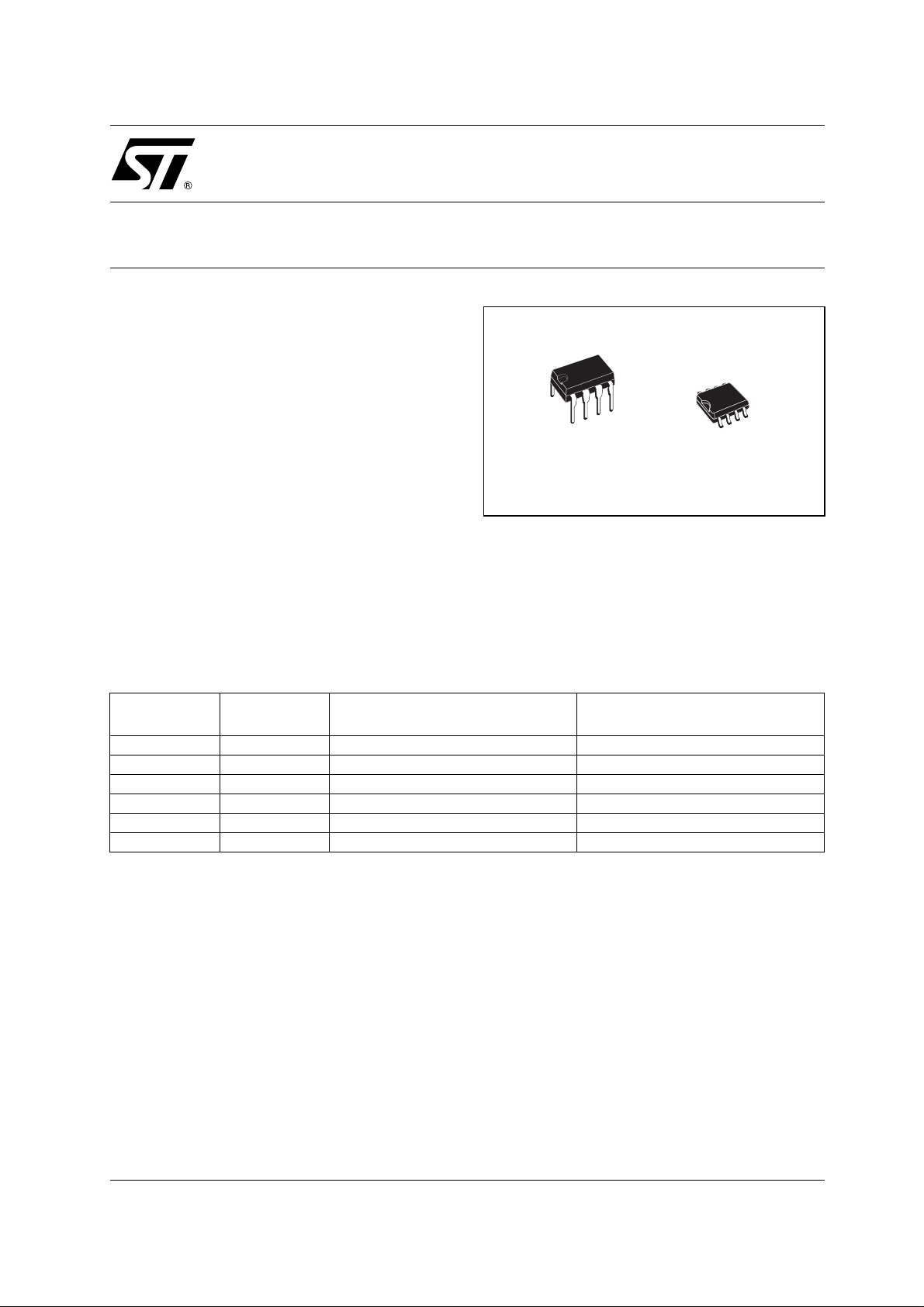
DIP SOP
ORDERING CODES
Type
ST490ACN 0 to 70 °C DIP-8 50parts per tube / 40tube per box
ST490ABN -40 to 85 °C DIP-8 50parts per tube / 40tube per box
ST490ACD 0 to 70 °C SO-8 (Tube) 100parts per tube / 20tube per box
ST490ABD -40 to 85 °C SO-8 (Tube) 100parts per tube / 20tube per box
ST490ACDR 0 to 70 °C SO-8 (Tape & Reel) 2500 parts per reel
ST490ABDR -40 to 85 °C SO-8 (Tape & Reel) 2500 parts per reel
Temperature
Range
Package Comments
1/11November 2002
Page 2

ST490A
PIN CONFIGURATION
PIN DESCRIPTION
PlN N° SYMBOL NAME AND FUNCTION
1
V
CC
2 RO Receiver Output.
3 DI Driver Input.
4 GND Ground
5 Z Inverting Driver Output
6 Y Non-inverting Driver Output
7 B Inverting Receiver Input
8 A Non-inverting Receiver Input
Supply Voltage
TRUTH TABLE (DRIV E R)
INPUT OUTPUTS
DI Y Z
LLH
HHL
X= Don’t Care; Z=High Impedance
TRUTH TABLE (RE CE IVER)
DIFFERENTIAL INPUT OUTPUT
A-B RO
≥ -0.2V H
between -0.2V to 0.2V ?
≤ -0.2V L
OPEN H
?= Irrelevant; Z=High Impedance
ABSOLUTE MAXIMUM RATINGS
Symbol Parameter Value Unit
V
V
V
Y,VZ
V
A,VB
V
RO
ESD Human Boby Model 3.5 KV
Absolute Maximum Ratings are those values beyond which damage to the device may occur. Functional operation under these condition is
not implied.
2/11
Supply Voltage
CC
Driver Input Voltage
DI
Driver Output Voltage
Receiver Input Voltage
Receiver Output Voltage -0.3 to (VCC+ 0.3)
7V
-0.5 to 7 V
-7.5 to 12.5 V
-7.5 to 12.5 V
V
Page 3

ST490A
ELECTRICAL CHARACTERISTICS
V
=4.5Vto5.5V,TA=-40to85°C, unless otherwise specified.Typicalvaluesare referred toTA=25°C)
CC
Symbol Parameter Test Conditions Min. Typ. Max. Unit
I
SUPPLY
C
TRANSMITTER E L ECTRICAL CHARACTERISTICS
V
CC
Symbol Parameter Test Conditions Min. Typ. Max. Unit
V
V
V
∆V
∆V
I
No Load Supply Current 2 5 mA
Input Capacitance 1.8 pF
C
IN
Driver Output Capacitance 1.2 pF
C
YZ
Output Capacitance 2.3 pF
OUT
=4.5Vto 5.5V,TA= -40to85°C,unlessotherwisespecified.TypicalvaluesarereferredtoTa= 25°C)
Differential Drive Output
OD1
(No load)
Differential Drive Output
OD2
(With Load)
Differential Drive Output
OD3
(With Load)
Change in magnitude of
OD
Driver Differential Output
RL=54Ω(RS-422) (Figure 1) 1.5 2.6 5 V
RL= 100Ω (RS-422) (Figure 1) 2 3 V
=54Ωor 100Ω (Figure 1) 0 0.2 V
R
L
Voltage for Complementary
Output States (Note1)
Driver Common Mode
V
OC
Output Voltage
Change in magnitude of
OC
Driver Common Mode
RL=54Ω(Figure 1) 1 3 V
RL=54Ω(Figure 1) 0 0.2 V
Output Voltage (Note1)
Power Off Output Current VCC=0V VO=-7V to 12V ± 100 µA
I
OFF
Driver Short Circuit Output
OSD
Current
Input Logic Threshold Low 0.8 V
V
IL
Input Logic Threshold High 2 V
V
IH
VO=-7V to 12V ± 35 ± 250 mA
V
CC
V
3/11
Page 4

ST490A
RECEIVER ELECTRICAL CHARACTERISTICS
V
=4.5Vto 5.5V,TA= -40to85°C,unlessotherwisespecified.TypicalvaluesarereferredtoTa= 25°C)
CC
Symbol Parameter Test Conditions Min. Typ. Max. Unit
I
Logic Input Current ± 2.0 µA
IN1
Input Current (A, B) other input=0V
I
V
∆V
V
V
R
I
OSR
IN2
Receiver Differential
TH
Threshold Voltage
Receiver Input Hysteresis VCM=0V 70 mV
TH
Receiver Output High
OH
Voltage
Receiver Output Low
OL
Voltage
Receiver Input Resistance VCM= -7V to 12V 12 24 KΩ
RIN
Receiver Short-Circuit
Current
= 0 or 5.25V
V
CC
VCM= -7V to 12V -0.2 0.2 V
I
= -8mA, VID= 200mV 3.5 4.7 V
OUT
I
= 8mA, VID= -200mV 0.2 0.4 V
OUT
VO=0VtoV
CC
DRIVER S WITCHING CHARACTERISTICS
=4.5Vto5.5V,TA=-40to85°C,unlessotherwisespecified.Typicalvaluesareref erred to Ta=25°C)
V
CC
Symbol Parameter Test Conditions Min. Typ. Max. Unit
Maximum Data Rate Jitter <5% 25 50 Mbps
D
R
t
PLH
t
PHL
t
SKEW
t
TLH
t
THL
Propagation Delay Input to
Output
Differential Output Delay
Skew
Rise or Fall Differential
Time
RL=54Ω CL1=CL2=50pF, (Figure 1) 10 16 ns
RL=54Ω CL1=CL2=50pF, (Figure 1) 1 3 ns
RL=54Ω CL1=CL2=50pF, (Figure 1) 8 12 ns
V
=12V 0.5 1 mA
IN
=-7V -0.35 -0.8 mA
V
IN
795mA
RECEIVER SWITCHING CHARACTERISTICS
=4.5Vto5.5V,TA=-40to85°C, unless otherwise specified.Typicalvaluesareref erred to Ta=25°C)
V
CC
Symbol Parameter Test Conditions Min. Typ. Max. Unit
Propagation Delay Input to
t
PLH
Output
t
PHL
t
SKD|tPLH -tPHL
Skew
t
t
Rise or Fall Time CL= 15pF (Figures 2,4) 8 ns
TLH
THL
4/11
|ReceiverOutput
CL= 15pF (Figures 2,4) 19 30 ns
CL= 15pF (Figures 2,4) 1 3 ns
Page 5

TEST CIRCUITS AND TYPICAL CHARACTERISTICS
Figure1 : Driver DC Test Load
Figure2 : Driver/Receiver TimingTest Circuit
ST490A
5/11
Page 6

ST490A
Figure3 : Driver Propagation Delay
Figure4 : Receiver Propagation Delay
6/11
Page 7

ST490A
Figure5 : Receiver Out put Current vs O utpu t
Voltage (Output Low)
Figure6 : Receiver Output Current vs Output
Voltage (Output High)
Figure8:DriverDiff. Output Voltage vs Com mon
Mode Voltage (Diff. Output High)
Figure9 : Driver Short Circuit Current vs L ine
Voltage (Output High)
Figure7:DriverDiff. Output Voltage vs Com mon
Mode Voltage (Diff. Output Low)
Figure10 : Driver Short Circuit Current vs. Line
Voltage (Output Low)
7/11
Page 8

ST490A
Figure11 : Receiver Inpu t Current vs Input
Voltage
8/11
Page 9

Plastic DIP-8 MECHANICAL DATA
ST490A
DIM.
MIN. TYP MAX. MIN. TYP. MAX.
A 3.3 0.130
a1 0.7 0.028
B 1.39 1.65 0.055 0.065
B1 0.91 1.04 0.036 0.041
b 0.5 0.020
b1 0.38 0.5 0.015 0.020
D 9.8 0.386
E 8.8 0.346
e 2.54 0.100
e3 7.62 0.300
e4 7.62 0.300
F 7.1 0.280
I 4.8 0.189
L 3.3 0.130
Z 0.44 1.6 0.017 0.063
mm. inch
P001F
9/11
Page 10

ST490A
SO-8 MECHANICAL DATA
DIM.
A 1.75 0.068
a1 0.1 0.25 0.003 0.009
a2 1.65 0.064
a3 0.65 0.85 0.025 0.033
b 0.35 0.48 0.013 0.018
b1 0.19 0.25 0.007 0.010
C 0.25 0.5 0.010 0.019
c1 45˚ (typ.)
D 4.8 5.0 0. 189 0.196
E 5.8 6.2 0.228 0.244
e 1.27 0.050
e3 3.81 0.150
F 3.8 4.0 0.149 0.157
L 0.4 1.27 0. 015 0.050
M 0.6 0. 023
S
MIN. TYP MAX. MIN. TYP. MAX.
mm. inch
˚ (max.)
8
10/11
0016023
Page 11

ST490A
Information furnished is believed to be accurate and reliable. However, STMicroelectronics assumes no responsibility f or the
consequences of use of such informatio n nor for any infringement of paten ts or o ther rig hts of t hird part ies which ma y result from
its use. No license is granted by implication or otherwise under any patent or patent rights of STMicroelectronics. Specifications
mentioned in this publication are subject to change without notice. This publication supersedes and replaces all information
previousl y suppl ied. STM icroel ectronics produc ts are not auth orized for use as c ritica l compone nts in l ife s upport dev ices or
systems without express written approval of STMicroelectronics.
Australia - Brazil - Canada - China - Finland - France - Germany - Hong Kong - India - Israel - Italy - Japan - Malaysia - Malta - Morocco
© The ST logo is a registered trademark of STMicroelectronics
© 2002 STMicroelectronics - Printed in Italy - All Rights Reserved
STMicroelectronics GROUP OF COMPANIES
Singapore - Spain - Sweden - Switzerland - United Kingdom - United States.
© http://www.st.com
11/11
 Loading...