

Datasheet ST485ADR, ST485CN, ST485CDR, ST485CD, ST485BN Datasheet (SGS Thomson Microelectronics)
...Page 1
1/12March 2002
■ LOW QUIESCENT CURRENT: 300µA
■ DESIGNED FOR RS-485 INTERFACE
APPLICATIONS
■ -7V TO 12V COMMON MODE INPUT
VOLTAGERANGE
■ DRIVER MAINTAINS HIGH IMPEDANCE IN
3-STATE OR WITH THE POWER OFF
■ 70mV TYPICAL INPUT HYSTERESIS
■ 30ns PROPAGATION DELAYS, 5ns SKEW
■ OPERATE FROM A SINGLE 5V SUPPLY
■ CURRENT LIMITING AND THERMAL
SHUTDOWN FOR DRIVER OVERLOAD
PROTECTION
■ ALLOWS UP TO 64 TRANSCEIVERS ON
THE BUS
DESCRIPTION
The ST485 is al low power transceiver for RS-485
and RS-422 communication. Each part contains
one driver and one receiver.
This transceiver draw 300µA (typ.) of supply
current when unloaded or fully loaded with
disabled drivers.
It operates from a single 5V supply.
Driver is short-circuit current limited and is
protected against excessive power dissipation by
thermal shutdown circuitry that placed the driver
outputs into a high-impedance state. .
The ST485 is designed for bi-directional data
communications on multipoint bus transmission
line (half-duplex applciations).
ORDERING CODES
Type
Temperature
Range
Package Comments
ST485CN 0 to 70 °C DIP-8 50parts per tube / 40tube per box
ST485BN -40 to 85 °C DIP-8 50parts per tube / 40tube per box
ST485AN -55 to 125 °C DIP-8 50parts per tube / 40tube per box
ST485CD 0 to 70 °C SO-8 (Tube) 100parts per tube / 20tube per box
ST485BN -40 to 85 °C DIP-8 50parts per tube / 40tube per box
ST485AD -55 to 125 °C SO-8 (Tube) 100parts per tube / 20tube per box
ST485CDR 0 to 70 °C SO-8 (Tape & Reel) 2500 parts per reel
ST485BDR -40 to 85 °C SO-8 (Tape & Reel) 2500 parts per reel
ST485ADR -55 to 125 °C SO-8 (Tape & Reel) 2500 parts per reel
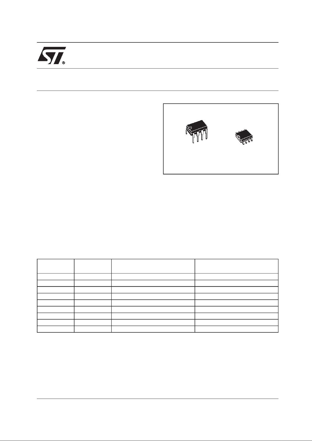
ST485
LOW POWER
RS-485/RS-422 TRANSCEIVER
DIP SOP
Page 2
ST485
2/12
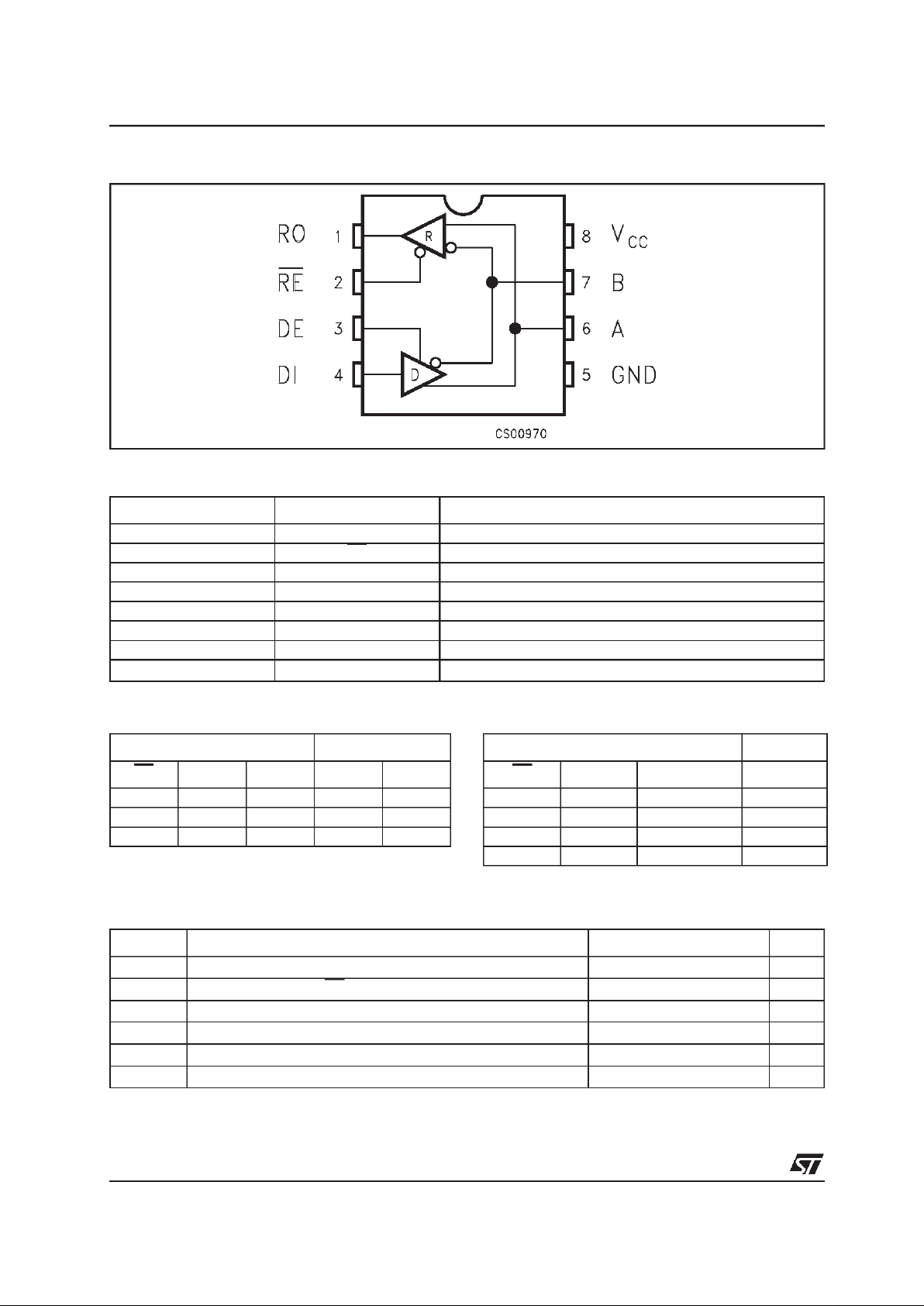
PIN CONFIGURATION
PIN DESCRIPTION
TRUTH TABLE (DRIVER)
X= Don’t Care; Z=High Impedance
TRUTH TABLE (RECEIVER)
X= Don’t Care; Z=High Impedance
ABSOLUTE MAXIMUM RATINGS
Absolute Maximum Ratings are those values beyond which damage to the device may occur. Functional operation under these condition is
not implied.
PlN N° SYMBOL NAME AND FUNCTION
1 RO Receiver Output
2 RE Receiver Output Enable
3 DE Driver Output Enable
4 DI Driver Input
5 GND Ground
6 A Non-inverting Receiver Input and Non-inverting Driver Output
7 B Inverting Receiver Input and Inverting Driver Output
8
V
CC
Supply Voltage
INPUTS OUTPUTS
RE DE DI B A
XHHLH
XHLHL
XLXZZ
INPUTS OUTPUT
RE DE A-B RO
LL≥ +0.2V H
LL≤ -0.2V L
L L INPUTS OPEN H
HL X Z
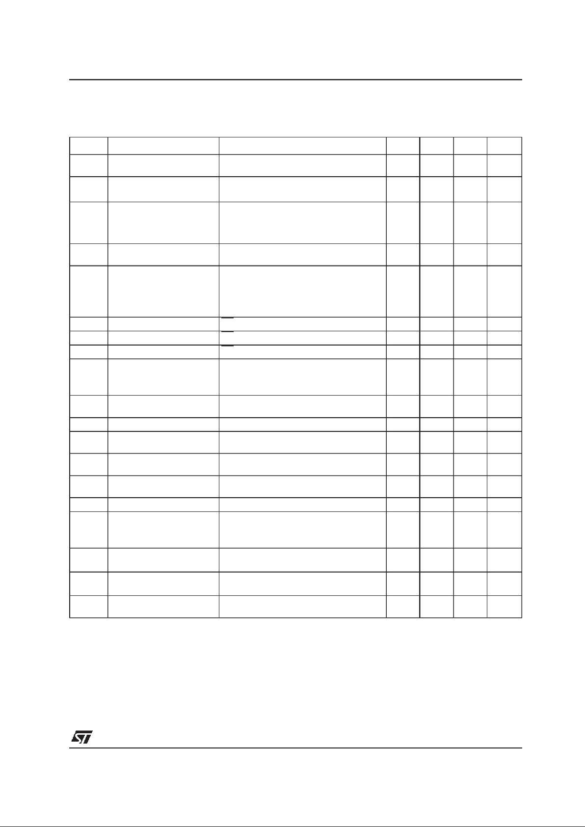
Symbol Parameter Value Unit
V
CC
Supply Voltage
12 V
V
I
Control Input Voltage (RE, DE) -0.5 to (VCC+ 0.5)
V
V
DI
Driver Input Voltage (DI) -0.5 to (VCC+ 0.5)
V
V
DO
Driver Output Voltage (A, B)
± 14 V
V
RI
Receiver Input Voltage (A, B)
± 14 V
V
RO
Receiver Output Voltage (RO) -0.5 to (VCC+ 0.5)
V
Page 3
ST485
3/12
DC ELECTRICAL CHARACTERISTICS
(VCC=5V± 5%, TA=T
MIN
toT
MAX
,unlessotherwise specified. Typicalvalues arereferredto TA=25°C)
(See Note 1)
Note 1: All currents into device pins are positive; all cuttents out of device pins are negative; all voltages are referenced to device ground
unless specified.
Note 2: Supply current specification is valid for loaded transmitters when V
DE
=0V
Note 3: Applies to peak current. See typical Operating Characteristics.
Symbol Parameter Test Conditions Min. Typ. Max. Unit
V
OD1
Differential Driver Output
(No Load)
5V
V
OD2
Differential Driver Output
(With Load)
RL=27Ω (RS-485) (See Fig. 1)
R
L
=50Ω (RS-422) (See Fig. 1)
1.4 5
5
V
V
∆V
OD
Change in Magnitude of
Driver Differential Output
Voltage for Complementary
Output States
RL=27Ω or 50Ω (See Fig. 1) 0.2 V
V
OC
Driver Common-Mode
Output Voltage
RL=27Ω or 50Ω (See Fig. 1) 3 V
∆V
OC
Change in Magnitude of
Driver Common-Mode
Output Voltage for
Complementary Output
States
RL=27Ω or 50Ω (See Fig. 1) 0.2 V
V
IH
Input High Voltage RE, DE, DI 2.0 V
V
IL
Input Low Voltage RE, DE, DI 0.8 V
I
IN1
Input Current RE, DE, DI ± 2 µA
I
IN2
Input Current (A, B) VCM= 0V or 5.25V VDE=0V
V
IN
= 12V
V
IN
= -7V
1
-0.8
mA
mA
V
TH
Receiver Differential
Threshold Voltage
VCM= -7 to 12V -0.2 0.2 V
∆V
TH
Receiver Input Hysteresis VCM=0V 70 mV
V
OH
Receiver Output High
Voltage
IO= -4mA VID= 200mV 3.4 V
V
OL
Receiver Output Low
Voltage
IO=4mA VID= -200mV 0.5 V
I
OZR
3-State (High Impedance)
Output Current at Receiver
VO= 0.4 to 2.4V ± 1 µA
R
IN
Receiver Input Resistance VCM= -7 to 12V 24 KΩ
I
CC
No Load Supply Current
(Note 2)
VRE=0VorV
CC
VDE=V
CC
VDE=0V
400
300
900
500
µA
µA
I
OSD1
Driver Short-Circuit Current,
V
O
=High
V
O
= -7 to 12V (Note 3) 35 250 mA
I
OSD2
Driver Short-Circuit Current,
V
O
=Low
V
O
= -7 to 12V (Note 3) 35 250 mA
I
OSR
Receiver Short-Circuit
Current
VO=0VtoV
CC
795mA
Page 4
ST485
4/12
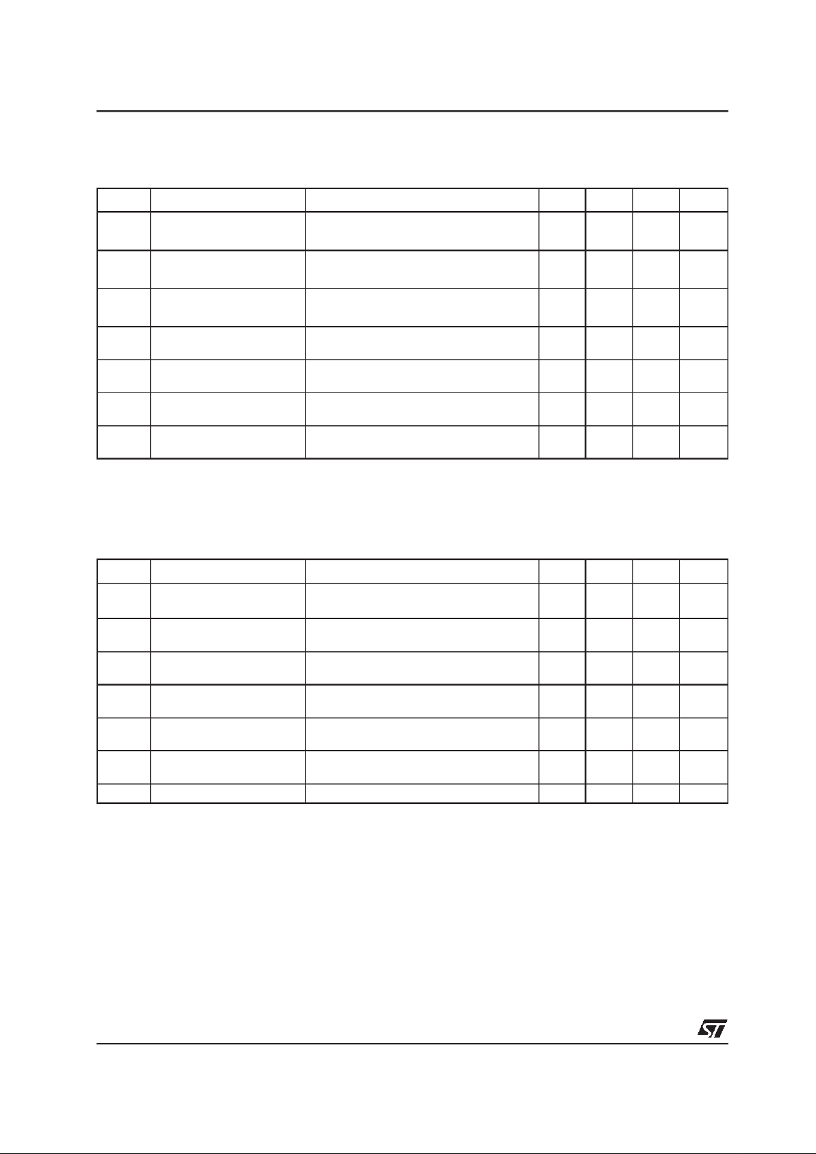
DRIVER SWITCHING CHARACTERISTICS
(VCC=5V ± 5%, TA=T
MIN
toT
MAX
,unless otherwise specified.Typical values are referred to TA=25°C)
(See Note 1)
Note 1: All currents into device pins are positive; all cuttents out of device pins are negative; all voltages are referenced to device ground
unless specified.
RECEIVER SWITCHING CHARACTERISTICS
(VCC=5V± 5%, TA=T
MIN
toT
MAX
,unlessotherwise specified. Typicalvalues arereferredto TA=25°C)
(See Note 1)
Note 1: All currents into device pins are positive; all cuttents out of device pins are negative; all voltages are referenced to device ground
unless specified.
Symbol Parameter Test Conditions Min. Typ. Max. Unit
t
PLH
t
PHL
Propagation Delay Input to
Output
R
DIFF
=54Ω CL1=CL2= 100pF
(See Fig. 3 and 5)
10 30 70 ns
t
SK
Output Skew to Output R
DIFF
=54Ω CL1=CL2= 100pF
(See Fig. 3 and 5)
510ns
t
TLH
t
THL
Rise or Fall Time R
DIFF
=54Ω CL1=CL2= 100pF
(See Fig. 3 and 5)
31545ns
t
PZH
Output Enable Time CL= 100pF S2 = Closed
(See Fig. 4 and 6)
70 90 ns
t
PZL
Output Enable Time CL= 100pF S1 = Closed
(See Fig. 4 and 6)
70 90 ns
t
PLZ
Output Disable Time CL= 15pF S1 = Closed
(See Fig. 4 and 6)
70 90 ns
t
PHZ
Output Disable Time CL= 15pF S2 = Closed
(See Fig. 4 and 6)
70 90 ns
Symbol Parameter Test Conditions Min. Typ. Max. Unit
t
PLH
t
PHL
Propagation Delay Input to
Output
R
DIFF
=54Ω CL1=CL2= 100pF
(See Fig. 3 and 7)
20 130 230 ns
t
SKD
Differential Receiver Skew R
DIFF
=54Ω CL1=CL2= 100pF
(See Fig. 3 and 7)
13 ns
t
PZH
Output Enable Time CRL= 15pF S1 = Closed
(See Fig. 2 and 8)
20 55 ns
t
PZL
Output Enable Time CRL= 15pF S2 = Closed
(See Fig. 2 and 8)
20 55 ns
t
PLZ
Output Disable Time CRL= 15pF S1 = Closed
(See Fig. 2 and 8)
20 55 ns
t
PHZ
Output Disable Time CRL= 15pF S2 = Closed
(See Fig. 2 and 8)
20 55 ns
f
MAX
Maximum Data Rate 2.5 Mbps
Page 5

ST485
5/12
TEST CIRCUITS AND TYPICAL CHARACTERISTICS
Figure 1 : Driver DC Test Load
Figure 2 : Receiver Timing Test Load
Figure 3 : Drive/Receiver Timing Test Circuit
Figure 4 : Driver Timing Test Load
Page 6

ST485
6/12
Figure 5 : Driver Propagation Delay
Figure 6 : Driver Enable and Disable Time
Page 7

ST485
7/12
Figure 7 : Receiver Propagation Delay
Figure 8 : Receiver Enable and Disable Time
Page 8

ST485
8/12
Figure 9 : Receiver Output Current vs Output
Low Voltage
Figure 10 : Receiver Output Current vs Output
High Voltage
Figure 11 : Driver Output Current vs Output Low
Voltage
Figure 12 : Driver Output Current vs Output High
Voltage
Figure 13 : Supply Current vs Temperature
Figure 14 : Receiver High Level Output Voltage
vs Temperature
Page 9

ST485
9/12
Figure 15 : Receiver Low Level Output Voltage
vs Temperature
Figure 16 : Differential Driver Output Voltage vs
Temperature
Page 10

ST485
10/12
DIM.
mm. inch
MIN. TYP MAX. MIN. TYP. MAX.
A 3.3 0.130
a1 0.7 0.028
B 1.39 1.65 0.055 0.065
B1 0.91 1.04 0.036 0.041
b 0.5 0.020
b1 0.38 0.5 0.015 0.020
D 9.8 0.386
E 8.8 0.346
e 2.54 0.100
e3 7.62 0.300
e4 7.62 0.300
F 7.1 0.280
I 4.8 0.189
L 3.3 0.130
Z 0.44 1.6 0.017 0.063
Plastic DIP-8 MECHANICAL DATA
P001F
Page 11

ST485
11/12
DIM.
mm. inch
MIN. TYP MAX. MIN. TYP. MAX.
A 1.75 0.068
a1 0.1 0.25 0.003 0.009
a2 1.65 0.064
a3 0.65 0.85 0.025 0.033
b 0.35 0.48 0.013 0.018
b1 0.19 0.25 0.007 0.010
C 0.25 0.5 0.010 0.019
c1 45° (typ.)
D 4.8 5.0 0.189 0.196
E 5.8 6.2 0.228 0.244
e 1.27 0.050
e3 3.81 0.150
F 3.8 4.0 0.149 0.157
L 0.4 1.27 0.015 0.050
M 0.6 0.023
S8°(max.)
SO-8 MECHANICAL DATA
0016023
Page 12

ST485
12/12
Information furnished is believed to be accurate and reliable. However, STMicroelectronics assumes no responsibility for the
consequences of use ofsuch information norfor anyinfringement of patents or otherrightsof third parties which mayresult from
its use. No license is granted by implication or otherwise under any patent or patent rights of STMicroelectronics. Specifications
mentioned in this publication are subject to change without notice. This publication supersedes and replaces all information
previously supplied. STMicroelectronics products are not authorized for use as critical components in life support devices or
systems without express written approval of STMicroelectronics.
TheST logo is a registered trademark of STMicroelectronics
2002 STMicroelectronics - Printed in Italy - All Rights Reserved
STMicroelectronics GRO UP OF CO MPANIES
Australia - Brazil - Canada - China - Finland - France - Germany - HongKong - India - Israel - Italy - Japan - Malaysia- Malta - Morocco
Singapore - Spain - Sweden - Switzerland - United Kingdom - United States.
http://www.st.com
 Loading...