

Page 1
DATASHEET
13 August 2003 ADCS 7260755H STMicroelectronics 1/94
Overview
The ST40RA is the first member of the ST40 family. Based
on the SH-4, SuperH CPU core from SuperH Inc, the
ST40RA is designed to work as a standalone device, or as
part of a two chip solution for application specific systems.
Example applications the ST40RA is designed for include
digital consumer, embedded communications, industrial
and automotive. The high connectivity of the ST40 through
its PCI bus and its dual memory uses makes it a versatile
device, ideal for data-intensive and high performance
applications.
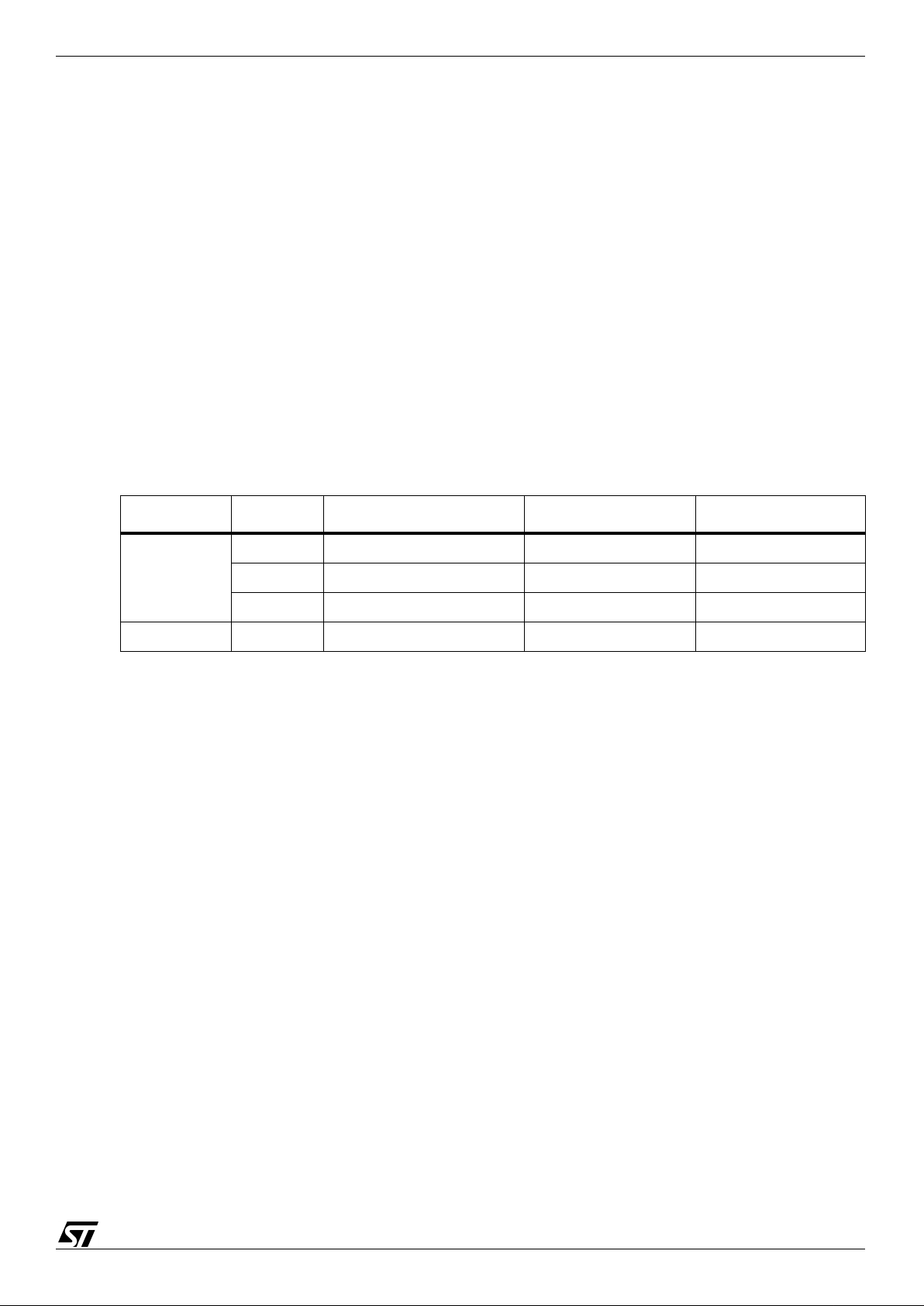
System features
■ 32-bit SuperH CPU
● 64-bit hardware FPU (1. 1 6 G F L O P S )
● 128-bit vector unit for matrix manipulations
● 166 MHz, 300 MIPS (DMIPS 1.1)
● Up to 664 Mbytes/s CPU bandwidth
● Direct mapped, on-chip, ICache (8 Kbytes) and DCache
(16 Kbytes)
■ High-performance 5-channel DMA engine,
supporting 1D or 2D block moves and linked lists
■ SuperHyway internal interco nne ct
● High throughput , low latency, split transact ion packet
router
■ Memory protection and VM system support
● 64-entry unified TLB, 4-entry instruction TLB
● 4 Gbytes address space
■ Standard ST40 peripherals
● 2 synchronous serial ports with FIFO (SCIF)
● Ti me rs and a real-time clock
IO devices
● Mailbox register for interprocessor comm unication
● Additional PIO
Bus interfaces
■ Local memory interface SDRAM & DDR SDRAM
● Up to 100 MHz (1.6 Gbytes/s peak throughput)
■ PCI interface - 32-bit, 66/33 MHz, 3.3 V
■ Enhanced memory interface (EMI)
● 32-bit bus, up to 83 MHz, for attaching peripherals
● High-speed, sync mode, burst flash ROM support
● SDRAM support
● MPX initiator and t arget interface
● Programmable MPX bus arbiter
Integer & FP
execution units
Registers
Interrupt ctrl
Real-time clock
Timer (TMU)
SCIF
Clock ctrl
SCIF
5 channel
controller
ST40 Local Memory I/F
32 data 64 data
32 data
2 channel
control
PIO
interface
JTAG
UDI
EMI
SuperHyway
PCI I/F 66MHz
Debug
PLLs
MMU
I Cache
MMU
D Cache
Cbus Bridge/
SuperHyway I/F
24 data
JTAG
DMA
PCI Peripherals SDRAM
MPX
Flash
Peripherals
Coprocessor
Mailbox
ST40RA
32-bit Embedded SuperH Device
Page 2

ADCS 7260755H STMicroelectronics 2/94
ST40RA
Table of Contents
Chapter 1 Scope of this document . . . . . . . . . . . . . . . . . . . . . . . . . . . . . . . . . . . . . . . . . . . . .6
Chapter 2 ST40 documentation suite . . . . . . . . . . . . . . . . . . . . . . . . . . . . . . . . . . . . . . . . . . .6
CPU documentation . . . . . . . . . . . . . . . . . . . . . . . . . . . . . . . . . . . . . . . . . . . . . . . . . . . . . . 6
System documentation . . . . . . . . . . . . . . . . . . . . . . . . . . . . . . . . . . . . . . . . . . . . . . . . . . . . 6
Chapter 3 ST40RA devices . . . . . . . . . . . . . . . . . . . . . . . . . . . . . . . . . . . . . . . . . . . . . . . . . .6
Chapter 4 Architecture . . . . . . . . . . . . . . . . . . . . . . . . . . . . . . . . . . . . . . . . . . . . . . . . . . . . . .7
4.1 Overview . . . . . . . . . . . . . . . . . . . . . . . . . . . . . . . . . . . . . . . . . . . . . . . . . . . . . . . . . . . . . . . 7
4.2 ST40 system . . . . . . . . . . . . . . . . . . . . . . . . . . . . . . . . . . . . . . . . . . . . . . . . . . . . . . . . . . . . 7
4.2.1 SuperH ST40 SH-4 core . . . . . . . . . . . . . . . . . . . . . . . . . . . . . . . . . . . . . . . . . . . . . . . . . . . . . . . . . . 7
4.2.2 SuperHyway internal interconnect . . . . . . . . . . . . . . . . . . . . . . . . . . . . . . . . . . . . . . . . . . . . . . . . . . . 8
4.2.3 Standard ST40 peripherals . . . . . . . . . . . . . . . . . . . . . . . . . . . . . . . . . . . . . . . . . . . . . . . . . . . . . . . . 8
4.3 Bus interfaces . . . . . . . . . . . . . . . . . . . . . . . . . . . . . . . . . . . . . . . . . . . . . . . . . . . . . . . . . . . 9
4.3.1 Local memory interface . . . . . . . . . . . . . . . . . . . . . . . . . . . . . . . . . . . . . . . . . . . . . . . . . . . . . . . . . . . 9
4.3.2 PCI interface . . . . . . . . . . . . . . . . . . . . . . . . . . . . . . . . . . . . . . . . . . . . . . . . . . . . . . . . . . . . . . . . . . 10
4.3.3 EMI/MPX interface . . . . . . . . . . . . . . . . . . . . . . . . . . . . . . . . . . . . . . . . . . . . . . . . . . . . . . . . . . . . . 10
4.4 I/O devices . . . . . . . . . . . . . . . . . . . . . . . . . . . . . . . . . . . . . . . . . . . . . . . . . . . . . . . . . . . . 10
4.4.1 Mailbox . . . . . . . . . . . . . . . . . . . . . . . . . . . . . . . . . . . . . . . . . . . . . . . . . . . . . . . . . . . . . . . . . . . . . . 10
4.5 Software . . . . . . . . . . . . . . . . . . . . . . . . . . . . . . . . . . . . . . . . . . . . . . . . . . . . . . . . . . . . . . 10
4.5.1 Development systems and software . . . . . . . . . . . . . . . . . . . . . . . . . . . . . . . . . . . . . . . . . . . . . . . . 10
4.5.2 Software compatibility . . . . . . . . . . . . . . . . . . . . . . . . . . . . . . . . . . . . . . . . . . . . . . . . . . . . . . . . . . . 11
Chapter 5 System configuration . . . . . . . . . . . . . . . . . . . . . . . . . . . . . . . . . . . . . . . . . . . . . .11
5.1 System addresses . . . . . . . . . . . . . . . . . . . . . . . . . . . . . . . . . . . . . . . . . . . . . . . . . . . . . . . 12
5.1.1 System address map . . . . . . . . . . . . . . . . . . . . . . . . . . . . . . . . . . . . . . . . . . . . . . . . . . . . . . . . . . . . 1 3
5.2 System identifiers . . . . . . . . . . . . . . . . . . . . . . . . . . . . . . . . . . . . . . . . . . . . . . . . . . . . . . . 14
5.3 Interrupt mapping . . . . . . . . . . . . . . . . . . . . . . . . . . . . . . . . . . . . . . . . . . . . . . . . . . . . . . . 15
5.3.1 ST40 core interrupt allocation . . . . . . . . . . . . . . . . . . . . . . . . . . . . . . . . . . . . . . . . . . . . . . . . . . . . . 15
5.3.2 ST40 standard system interrupt allocation . . . . . . . . . . . . . . . . . . . . . . . . . . . . . . . . . . . . . . . . . . . 16
5.3.3 ST40RA I/O device interrupt allocation . . . . . . . . . . . . . . . . . . . . . . . . . . . . . . . . . . . . . . . . . . . . . . 17
5.4 GPDMA channel mapping . . . . . . . . . . . . . . . . . . . . . . . . . . . . . . . . . . . . . . . . . . . . . . . . . 17
5.5 EMI DACK mapping . . . . . . . . . . . . . . . . . . . . . . . . . . . . . . . . . . . . . . . . . . . . . . . . . . . . . 18
5.6 EMI address pin mapping . . . . . . . . . . . . . . . . . . . . . . . . . . . . . . . . . . . . . . . . . . . . . . . . . 18
Page 3

ST40RA
3/94 STMicroelectronics ADCS 7260755H
5.7 EMI pin to function relationship . . . . . . . . . . . . . . . . . . . . . . . . . . . . . . . . . . . . . . . . . . . . . 19
5.8 Memory bridge control . . . . . . . . . . . . . . . . . . . . . . . . . . . . . . . . . . . . . . . . . . . . . . . . . . . 21
5.8.1 Memory bridge control signals . . . . . . . . . . . . . . . . . . . . . . . . . . . . . . . . . . . . . . . . . . . . . . . . . . . . 22
5.8.2 Memo ry bridge status . . . . . . . . . . . . . . . . . . . . . . . . . . . . . . . . . . . . . . . . . . . . . . . . . . . . . . . . . . . 22
5.8.3 Changing control of a memory bridge . . . . . . . . . . . . . . . . . . . . . . . . . . . . . . . . . . . . . . . . . . . . . . . 22
5.9 System configuration registers . . . . . . . . . . . . . . . . . . . . . . . . . . . . . . . . . . . . . . . . . . . . . 23
5.9.1 EMI.GENCFG EMI general configuration . . . . . . . . . . . . . . . . . . . . . . . . . . . . . . . . . . . . . . . . . . . . 24
5.9.2 LMI.COC . . . . . . . . . . . . . . . . . . . . . . . . . . . . . . . . . . . . . . . . . . . . . . . . . . . . . . . . . . . . . . . . . . . . . 2 5
5.9.3 LMI.CIC . . . . . . . . . . . . . . . . . . . . . . . . . . . . . . . . . . . . . . . . . . . . . . . . . . . . . . . . . . . . . . . . . . . . . . 26
5.9.4 SYSCO NF registers . . . . . . . . . . . . . . . . . . . . . . . . . . . . . . . . . . . . . . . . . . . . . . . . . . . . . . . . . . . . 26
5.9.5 SYSCONF.SYS_CON2. . . . . . . . . . . . . . . . . . . . . . . . . . . . . . . . . . . . . . . . . . . . . . . . . . . . . . . . . . 27
5.9.6 PIO alternate fu nctions . . . . . . . . . . . . . . . . . . . . . . . . . . . . . . . . . . . . . . . . . . . . . . . . . . . . . . . . . . 2 9
5.9.7 PCI.PERF register definition. . . . . . . . . . . . . . . . . . . . . . . . . . . . . . . . . . . . . . . . . . . . . . . . . . . . . . 30
Chapter 6 Clock generation . . . . . . . . . . . . . . . . . . . . . . . . . . . . . . . . . . . . . . . . . . . . . . . . .30
6.1 Clock domains and sources . . . . . . . . . . . . . . . . . . . . . . . . . . . . . . . . . . . . . . . . . . . . . . . 30
6.2 Recommended operating modes . . . . . . . . . . . . . . . . . . . . . . . . . . . . . . . . . . . . . . . . . . . 34
6.3 Clocks and registers at start up . . . . . . . . . . . . . . . . . . . . . . . . . . . . . . . . . . . . . . . . . . . . . 34
6.3.1 CLOCKGENA_2x PCI (PCI_DIV_BYPASS = 0) . . . . . . . . . . . . . . . . . . . . . . . . . . . . . . . . . . . . . . . 3 5
6.3.2 Division ratios on CLOCKGENA_2x. . . . . . . . . . . . . . . . . . . . . . . . . . . . . . . . . . . . . . . . . . . . . . . . . 35
6.4 Setting clock frequencies . . . . . . . . . . . . . . . . . . . . . . . . . . . . . . . . . . . . . . . . . . . . . . . . . 36
6.4.1 Programming the PLL output frequency . . . . . . . . . . . . . . . . . . . . . . . . . . . . . . . . . . . . . . . . . . . . . 37
6.4.2 Changing clock frequency . . . . . . . . . . . . . . . . . . . . . . . . . . . . . . . . . . . . . . . . . . . . . . . . . . . . . . . . 37
6.4.3 Changing the core PLL frequencies . . . . . . . . . . . . . . . . . . . . . . . . . . . . . . . . . . . . . . . . . . . . . . . . 37
6.4.4 Changing the frequency division ratio . . . . . . . . . . . . . . . . . . . . . . . . . . . . . . . . . . . . . . . . . . . . . . . 38
6.5 Power management . . . . . . . . . . . . . . . . . . . . . . . . . . . . . . . . . . . . . . . . . . . . . . . . . . . . . 38
6.5.1 CPU low-power modes . . . . . . . . . . . . . . . . . . . . . . . . . . . . . . . . . . . . . . . . . . . . . . . . . . . . . . . . . . 38
6.5.2 Module low-power modes . . . . . . . . . . . . . . . . . . . . . . . . . . . . . . . . . . . . . . . . . . . . . . . . . . . . . . . . 38
6.6 Clock generation registers . . . . . . . . . . . . . . . . . . . . . . . . . . . . . . . . . . . . . . . . . . . . . . . . 38
6.6.1 CLOCKGENB.CLK_SELCR register . . . . . . . . . . . . . . . . . . . . . . . . . . . . . . . . . . . . . . . . . . . . . . . 39
6.6.2 CPG.STBCR register . . . . . . . . . . . . . . . . . . . . . . . . . . . . . . . . . . . . . . . . . . . . . . . . . . . . . . . . . . 40
6.6.3 CLOCKGENA.STBREQCR and CLOC KGEN B.STBRE QCR registers . . . . . . . . . . . . . . . . . . . . . . 41
6.6.4 CLOCKGENA.STBREQCR_SET and CLOCKGENB.STBREQCR_SET registers . . . . . . . . . . . . . 41
6.6.5 CLOCKGENA.STBREQCR_CLR and CLOCKGENB.STBREQCR_CLR register . . . . . . . . . . . . 4 1
6.6.6 CLOCKGENA.STBACKCR and CLOCKGENB.STBACKCR register . . . . . . . . . . . . . . . . . . . . . . 42
Chapter 7 Electrical specifications . . . . . . . . . . . . . . . . . . . . . . . . . . . . . . . . . . . . . . . . . . .43
7.1 DC absolute maximum ratings . . . . . . . . . . . . . . . . . . . . . . . . . . . . . . . . . . . . . . . . . . . . . 43
Page 4

ADCS 7260755H STMicroelectronics 4/94
ST40RA
7.1.1 Fmax clock domains . . . . . . . . . . . . . . . . . . . . . . . . . . . . . . . . . . . . . . . . . . . . . . . . . . . . . . . . . . . 43
7.1.2 Ope rating conditions . . . . . . . . . . . . . . . . . . . . . . . . . . . . . . . . . . . . . . . . . . . . . . . . . . . . . . . . . . . 44
7.1.3 Pad specific output AC characteristics . . . . . . . . . . . . . . . . . . . . . . . . . . . . . . . . . . . . . . . . . . . . . 45
7.2 Rise and fall times . . . . . . . . . . . . . . . . . . . . . . . . . . . . . . . . . . . . . . . . . . . . . . . . . . . . . 47
7.3 PCI interface AC specifications . . . . . . . . . . . . . . . . . . . . . . . . . . . . . . . . . . . . . . . . . . . 50
7.4 LMI interface (SDRA M) AC specifications . . . . . . . . . . . . . . . . . . . . . . . . . . . . . . . . . . . 51
7.5 LMI interface (DDR-SDRAM) AC specifications . . . . . . . . . . . . . . . . . . . . . . . . . . . . . . . 52
7.6 DDR bus termination (SSTL_2) . . . . . . . . . . . . . . . . . . . . . . . . . . . . . . . . . . . . . . . . . . . . 53
7.7 General purpose periph eral bus (EMI ) AC specific at ions . . . . . . . . . . . . . . . . . . . . . . . 54
7.8 PIO AC specifications . . . . . . . . . . . . . . . . . . . . . . . . . . . . . . . . . . . . . . . . . . . . . . . . . . . . 55
7.9 System CLKIN AC specifications . . . . . . . . . . . . . . . . . . . . . . . . . . . . . . . . . . . . . . . . . . . 56
7.10 Low power CLKIN AC specifications . . . . . . . . . . . . . . . . . . . . . . . . . . . . . . . . . . . . . . . . . 57
7.11 UDI and IEEE 1149.1 TAP AC specifications . . . . . . . . . . . . . . . . . . . . . . . . . . . . . . 58
Chapter 8 Pin description . . . . . . . . . . . . . . . . . . . . . . . . . . . . . . . . . . . . . . . . . . . . . . . . . . .59
8.1 Function pin use selection . . . . . . . . . . . . . . . . . . . . . . . . . . . . . . . . . . . . . . . . . . . . . . . . . 59
8.2 Mode selection . . . . . . . . . . . . . . . . . . . . . . . . . . . . . . . . . . . . . . . . . . . . . . . . . . . . . . . . . 59
8.3 PBGA 27 x 27 ba llout . . . . . . . . . . . . . . . . . . . . . . . . . . . . . . . . . . . . . . . . . . . . . . . . . . . . 61
8.4 Pin states . . . . . . . . . . . . . . . . . . . . . . . . . . . . . . . . . . . . . . . . . . . . . . . . . . . . . . . . . . . . . 72
Chapter 9 Package . . . . . . . . . . . . . . . . . . . . . . . . . . . . . . . . . . . . . . . . . . . . . . . . . . . . . . . . .75
Appendix A Interconnect architecture. . . . . . . . . . . . . . . . . . . . . . . . . . . . . . . . . . . . . . . . . . .78
A.1 Arbitration scheme s . . . . . . . . . . . . . . . . . . . . . . . . . . . . . . . . . . . . . . . . . . . . . . . . . . . . . . 79
A.1.1 PCI arbiter: (CPU, GPDMA, PCI, EMPI) . . . . . . . . . . . . . . . . . . . . . . . . . . . . . . . . . . . . . . . . . . . . 79
A.1.2 EMI arbiter: (CPU buffer, GPDMA, PCI, EMPI) . . . . . . . . . . . . . . . . . . . . . . . . . . . . . . . . . . . . . . . . 79
A.1.3 LMI 1 arbiter: (CPU, GPDMA, PCI, EMPI). . . . . . . . . . . . . . . . . . . . . . . . . . . . . . . . . . . . . . . . . . . . 79
A.1.4 PER arbiter: (CPU, GPDMA, PCI, EMPI). . . . . . . . . . . . . . . . . . . . . . . . . . . . . . . . . . . . . . . . . . . . . 79
A.1.5 LMI2 arbiter: (CPU, GPDMA, PCI, EMPI) . . . . . . . . . . . . . . . . . . . . . . . . . . . . . . . . . . . . . . . . . . . . 80
A.1.6 Return arbitration . . . . . . . . . . . . . . . . . . . . . . . . . . . . . . . . . . . . . . . . . . . . . . . . . . . . . . . . . . . . . . . 80
A.2 Interconnect registers. . . . . . . . . . . . . . . . . . . . . . . . . . . . . . . . . . . . . . . . . . . . . . . . . . . . . 80
A.2.1 LMI1 arbiter . . . . . . . . . . . . . . . . . . . . . . . . . . . . . . . . . . . . . . . . . . . . . . . . . . . . . . . . . . . . . . . . . . . 81
A.2.2 LMI2 arbiter . . . . . . . . . . . . . . . . . . . . . . . . . . . . . . . . . . . . . . . . . . . . . . . . . . . . . . . . . . . . . . . . 82
A.2.3 EMI arbiter . . . . . . . . . . . . . . . . . . . . . . . . . . . . . . . . . . . . . . . . . . . . . . . . . . . . . . . . . . . . . . . . . . . 83
A.2.4 PCI arbiter . . . . . . . . . . . . . . . . . . . . . . . . . . . . . . . . . . . . . . . . . . . . . . . . . . . . . . . . . . . . . . . . . . 84
A.2.5 Peripheral arbiter . . . . . . . . . . . . . . . . . . . . . . . . . . . . . . . . . . . . . . . . . . . . . . . . . . . . . . . . . . . . . 85
Appendix B Implementation restrictions . . . . . . . . . . . . . . . . . . . . . . . . . . . . . . . . . . . . . . . . .87
Page 5

ST40RA
5/94 STMicroelectronics ADCS 7260755H
B.1 ST40 CPU . . . . . . . . . . . . . . . . . . . . . . . . . . . . . . . . . . . . . . . . . . . . . . . . . . . . . . . . . . . . . 87
B.1.1 tas.b . . . . . . . . . . . . . . . . . . . . . . . . . . . . . . . . . . . . . . . . . . . . . . . . . . . . . . . . . . . . . . . . . . . . . . . . . 87
B.1.2 Store que ue power-down. . . . . . . . . . . . . . . . . . . . . . . . . . . . . . . . . . . . . . . . . . . . . . . . . . . . . . . . . 8 7
B.1.3 UBC power-down . . . . . . . . . . . . . . . . . . . . . . . . . . . . . . . . . . . . . . . . . . . . . . . . . . . . . . . . . . . . . . . 87
B.1.4 Sy stem standby . . . . . . . . . . . . . . . . . . . . . . . . . . . . . . . . . . . . . . . . . . . . . . . . . . . . . . . . . . . . . . . . 87
B.2 PCI. . . . . . . . . . . . . . . . . . . . . . . . . . . . . . . . . . . . . . . . . . . . . . . . . . . . . . . . . . . . . . . . . . . 87
B.2.1 Clocking . . . . . . . . . . . . . . . . . . . . . . . . . . . . . . . . . . . . . . . . . . . . . . . . . . . . . . . . . . . . . . . . . . . . . . 87
B.2.2 Type 2 configuration accesses. . . . . . . . . . . . . . . . . . . . . . . . . . . . . . . . . . . . . . . . . . . . . . . . . . . . . 8 7
B.2.3 Software visible chang es between STB1HC7 and ST40RA H8D . . . . . . . . . . . . . . . . . . . . . . . . . . . 8 7
B.2.4 Error behavior . . . . . . . . . . . . . . . . . . . . . . . . . . . . . . . . . . . . . . . . . . . . . . . . . . . . . . . . . . . . . . . . . . 87
B.2.5 Mas ter abort . . . . . . . . . . . . . . . . . . . . . . . . . . . . . . . . . . . . . . . . . . . . . . . . . . . . . . . . . . . . . . . . . . . 88
B.3 EMI/EMPI. . . . . . . . . . . . . . . . . . . . . . . . . . . . . . . . . . . . . . . . . . . . . . . . . . . . . . . . . . . . . . 88
B.3.1 EMPI burst mode operation: ST40RA MPX target. . . . . . . . . . . . . . . . . . . . . . . . . . . . . . . . . . . . . . 8 8
B.3.2 SDRAM initialization during boot from flash. . . . . . . . . . . . . . . . . . . . . . . . . . . . . . . . . . . . . . . . . . . 88
B.3.3 MPX boot . . . . . . . . . . . . . . . . . . . . . . . . . . . . . . . . . . . . . . . . . . . . . . . . . . . . . . . . . . . . . . . . . . . . . 88
B.4 Ma ilbox. . . . . . . . . . . . . . . . . . . . . . . . . . . . . . . . . . . . . . . . . . . . . . . . . . . . . . . . . . . . . . . . 88
B.4.1 Test and set f unctionali ty . . . . . . . . . . . . . . . . . . . . . . . . . . . . . . . . . . . . . . . . . . . . . . . . . . . . . . . . . 88
B.5 Power down . . . . . . . . . . . . . . . . . . . . . . . . . . . . . . . . . . . . . . . . . . . . . . . . . . . . . . . . . . . . 88
B.5.1 Module power-down sequencing . . . . . . . . . . . . . . . . . . . . . . . . . . . . . . . . . . . . . . . . . . . . . . . . . . . 88
B.5.2 Acce sses to modules in power-down state . . . . . . . . . . . . . . . . . . . . . . . . . . . . . . . . . . . . . . . . . . . 88
B.6 PIO. . . . . . . . . . . . . . . . . . . . . . . . . . . . . . . . . . . . . . . . . . . . . . . . . . . . . . . . . . . . . . . . . . . 89
B.6.1 PIO defa u lt fun c ti onali t y foll o w i n g r e s e t . . . . . . . . . . . . . . . . . . . . . . . . . . . . . . . . . . . . . . . . . . . . . . 89
B.6.2 PCI/PIO alternate functions . . . . . . . . . . . . . . . . . . . . . . . . . . . . . . . . . . . . . . . . . . . . . . . . . . . . . . . 89
B.7 Interconnect . . . . . . . . . . . . . . . . . . . . . . . . . . . . . . . . . . . . . . . . . . . . . . . . . . . . . . . . . . . . 90
B.7.1 Memo ry bridge functionality . . . . . . . . . . . . . . . . . . . . . . . . . . . . . . . . . . . . . . . . . . . . . . . . . . . . . . . 90
B.7.2 Clock selection . . . . . . . . . . . . . . . . . . . . . . . . . . . . . . . . . . . . . . . . . . . . . . . . . . . . . . . . . . . . . . . . . 90
B.7.3 Pad drive control . . . . . . . . . . . . . . . . . . . . . . . . . . . . . . . . . . . . . . . . . . . . . . . . . . . . . . . . . . . . . . . 90
B.8 GPDMA . . . . . . . . . . . . . . . . . . . . . . . . . . . . . . . . . . . . . . . . . . . . . . . . . . . . . . . . . . . . . . . 90
B.8.1 Linked list support . . . . . . . . . . . . . . . . . . . . . . . . . . . . . . . . . . . . . . . . . . . . . . . . . . . . . . . . . . . . . . 90
B.8.2 2-D transfers . . . . . . . . . . . . . . . . . . . . . . . . . . . . . . . . . . . . . . . . . . . . . . . . . . . . . . . . . . . . . . . . . . . 90
B.8.3 Protocol signals . . . . . . . . . . . . . . . . . . . . . . . . . . . . . . . . . . . . . . . . . . . . . . . . . . . . . . . . . . . . . . . . 90
Revision history . . . . . . . . . . . . . . . . . . . . . . . . . . . . . . . . . . . . . . . . . . . . . . . . . . . . . . . . . . . . . .91
Page 6
ADCS 7260755H STMicroelectronics 6/94
ST40RA
1 Scope of this document
1 Scope of this document
This docum ent describ es only th os e areas of the ST40R A that are device sp ec if ic , for example the
system address map. Infor mation that is generic to the ST40 family of devices is containe d in the
ST40 documentation suite.
2 ST40 documentation suite
This document references a number of other generic ST40 documents that combined together form
a complete datasheet.
CPU documentation
The SH- 4 C PU core and it s ins t ruction set are documented in the
SH-4 CP U Co re Architec tu re
Manual
.
System documentation
Devices listed in the system address map,
Figure 2 on page 13
are docum ent ed in the
ST40
System Architecture Manual
:
●
Volume 1: System
, details the ST 40 CPU and s t andard peripherals,
●
Volume 2: Bus In t erf ac es
, details the standard PC I , L M I a nd EMI bus interfaces.
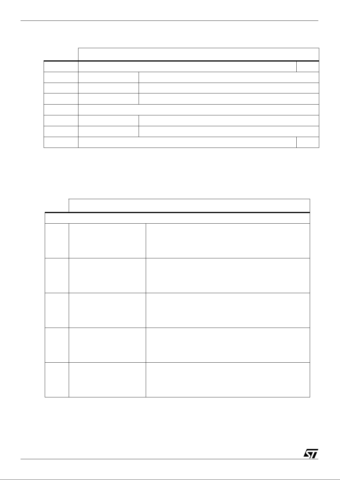
3 ST40RA devices
Device CPU clock frequency
Te m pera ture ran ge
Minimum Maximum
ST40RA150XHA 150 MHz
-40
o
C +85
o
C
ST40RA166XH1 166 MHz
0
o
C +70
o
C
ST40RA166XH6 166 MHz
-40
o
C +85
o
C
ST40RA200XH6 200 MHz
-40
o
C +85
o
C
Table 1: ST40RA device types
Page 7
4 Architect
ure
ST40RA
7/94 STMicroelectronics ADCS 7260755H
4 Architecture
4.1 Overview
The ST4 0R A combines an SH-4, 32-bit micro processor wi th a w ide range of in t erf ac es to external
periph erals. This se c tio n briefly des c ribes each of th e fe at ures of the S T 40RA.
4.2 ST40 system
4.2.1 SuperH ST40 SH-4 core
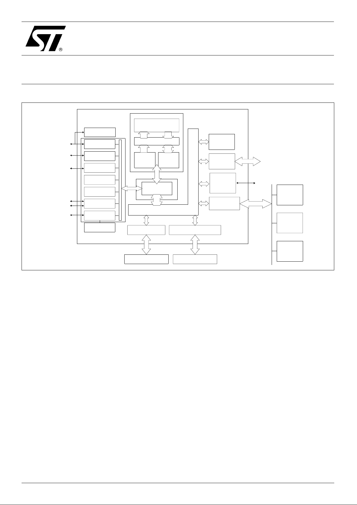
Figure 1
illustrates t he system architecture of the ST40 SH-4 core. The following section briefly
describes the features and performance of the core.
Central processing unit
The cen tr al processin g unit is built ar ound a 32-bit R IS C , two-way sup erscalar arc hitecture .
Operating at 166 MHz it runs with high code density using fixed length 16-bit instructions. It has a
load/store architec t ure, delayed branch ins t ruc t ion capabi lit y a nd an on-chi p m ult iplier. It uses a
five-stage pipeline.
Figure 1: ST40 SH-4 core architecture
CPU
UBC
FPU
ICache 8 Kbytes ITLB UTLB
Cache and TLB
controller
DCache 16 Kbytes
29bit add
32bit data
32bit data
32-bi t add (instruction)
32-b it data (instruction)
32-bit address (data)
32-bit data (load)
32-it data (store)
Lower 32-bit data
Lower 32-bit data
64-bit data (store)
Upper 32-bit data
Page 8

ADCS 7260755H STMicroelectronics 8/94
ST40RA
4 Architect
ure
Floating point unit/m ultiply and accumulate
The on-c hip, floatin g point coproc essor exe cu t es s ingle precision (32-bit ) and double precision
(64-bit) operation s . It has a f iv e-stage pipeline and su pports IEEE 754-compliant data t yp es and
exceptions. It has rounding mo des: (round-t o-neares t ) and (round-t o-zero), and handles
denormalized nu m bers (trunc at ion-to-zero) or interru pt generation fo r c om pliance wit h I EEE754.
The floa ti ng point unit performs the following f unctions:
● fmac (multiply-and-accumulate), fdiv (divide),
● fsqrt (sq uare root) in s tr uc t ions,
● 3-D graphics ins tr uc t ions (single-precision):
➢ 4-dimens ional vecto r c onversion and matrix operations (ft rv ): 4 cycles (pitch), 7 cycles
(latency),
➢ 4-dimensional vector (fipr) inner product: 1 cycle (pitch), 4 cycles (latency).
MMU configuration
There is 4 Gbytes virtual address space with 256 address space identifiers (8-bit ASIDs),
support ing single virt ual and mu lti ple virtual me m ory modes . P age sizes are 1 Kbyte, 4 Kbyt es , 64
Kbytes or 1 Mbyte. The MMU supports four-entry, fully associative ITLB for instructions and
64-entry fully associative UTLB for instructions and operands. Software-controlled replacement and
random-counter replacement algori th m s are also supported. Th e physical ad dress space is 512
Mbytes (29-bit), see
Figure 2: System address organization on page 12
.
Cache
8 Kbyte s o f di rec t -m apped ins t ruc t ion cache are organiz ed as 256 32-b y t e lines, and 16 Kbytes of
direct-mapped operand cache are organized as 512 32-byte lines. RAM mode (8-Kbyte cache plus
8-Kbyt e R AM ) with sele ctable write m et hod (copy back or write t hrough) is supported . A sin gle
stage bu ffer f or c opy-back and a single st age buffer for writ e-through are availab le. T he c ache
conten ts c an be addres s m apped and t here is a 32-b yte two-entr y store queue.
4.2.2 SuperHyway internal interconnect
The ST4 0R A uses the SuperHyw ay m em ory mapped packet rout er for on-chip intermodule
communication. T he interconnect suppo rt s a s plit t ransaction system allowing a nonblocking high
throughput, low latency system to be built. There are separate request and response packet
routers.
The ST40RA SuperHyway implementation is show in
Section 5. 8: Memory bridge con t rol on
page 21
. The interconnect allows simultaneous requests between multiple modules and is able to
ensure a v ery high data through put with in many c as es zero rout ing, arbitrat ion and dec ode
latencies.
4.2.3 Standard ST40 peripherals
Synchronous serial channel
There are two ST40 co m patible full duplex com m unication c hannels (S C IF1, SCIF2).
Asynchronous mode is supported. A se parate 16-b y te F IFO is provided for the tra ns m it t er and
receive r.
Interrupt controller
The inte rrupt contro ller supports all of the on-c hip peripheral module int errupts, an d f iv e ex t ernal
interrupts (NMI and IRL0 to IRL3). The priority can be set for each on-chip pe ripheral mo dule
interrupt . IRL0 to IRL3 are configured as four independent interrupt s or encoded to prov ide 15
external interrupt levels.
Page 9

4 Architect
ure
ST40RA
9/94 STMicroelectronics ADCS 7260755H
Debug controller
Debugging is performed by break interrupts. There are two break channels. The ad dress, data
value, access type, and data size can all be set as break conditions. Sequential break functions are
supported.
The user debug interface (UDI) contains a five-pin serial inte rfa c e c onforming t o J TAG, IEEE
Standard TA P and boundary scan a rc hit ecture. The interfac e provides hos t ac c es s t o t he 1 Kbyte
ASERAM for emu lat or firmware (ac c es s ible only in A SE mode).
Timers
The thre e-c hannel, a ut o-reload, 3 2-bit timer ha s an input capt ure function and a choice of s ev en
counter input clocks.
Real-time clock
The built -in 32-kHz cry s t al oscillator has a m aximum 1 /2 56 second res olution. It has dynam ic ally
progra m m able operat ing frequen c ies and on-ch ip c loc k and calend ar function s . It h as two sleep
modes and one standby mode.
Watchdog timer
The ST4 0R A has an 8-b it w at c hdog timer (W D T ) w it h program m able clock ra ti o. Th e W D T is able
to generate a power-on reset or a manual res et .
Programmable PLLs
The ST4 0R A has three program m able PLLs. T he PLLs are configured by M OD E pins at res et and
then reconfigured by software to optimize system performance or reduce system power
consumption.
General-purpose DMA controller
The five-c hannel phy s ic al address GPDMA c ont roller has four general-purpos e c hannels for
memory-to-memory or memory-to-peripheral transfers, and one buffered multiplexed channel. Both
2-D block moves and linked lists are suppor te d. Two sets of DMA handshake pins are available for
use by ext ernal devices to suppo rt effic ient transfer interdevic e transfers v ia external int erfaces
such as the EMI MPX.
Parallel I/O module
24 bits of parallel I/O are provided from t he ST40 com patible PIO. Eac h bit is program m able as an
output or an input. “Inp ut c om pare” generates an int errupt on a ny ch ange of any input bit.
4.3 Bus interfaces
4.3.1 Local memory interface
The LMI supports 16-, 3 2- a nd 64- bit wide bus SDRAM and DDR SDRAM, at up to 100 MHz with a
maximum address space of 112 Mbytes. Devices supported include two and four bank 16- , 64-,
128- an d 256-Mbit te c hnologies in x4 , x8 , x16 and x32 pac k ages. The LM I pads are dua l m ode
pads electrically compatible with L VTTL (for standard SDRAM) and SSTL_2 (for DDR SDRAM). For
full deta il of th e c onfiguration options of t he LMI pleas e s ee
ST40 System Architecture Manual,
Volume 2: Bus I nt erfaces
.
Page 10

ADCS 7260755H STMicroelectronics 10/94
ST40RA
4 Architect
ure
4.3.2 PCI interface
The PCI interface co mplies to the
PCI v2.1
and
Power Management Interface V1.0
specifications. It
is 32 bits wide and operates at 33 or 66 MHz. Master and target mode are supported. A PCI arbiter
and clock generator is provided inside the ST40RA. For details on the configuration options for the
PCI interf ace please s ee
ST40 System Architecture Manual, Volume 2: Bus Interfaces
.
4.3.3 EMI/MPX interface
The EMI/MPX interface contains the fol lowi ng blo cks. Fo r full details of the configuration options of
the EMI please see the
ST40 System Architecture Manual, Volume 2: Bus Inter faces
.
EMI memory interface initiator
The EM I pr ov ides access t o R OMs, SDR AM , m em ory mapped asynch ronous ext ernal peripherals
and syn ch ronous MPX bus perip herals. The EM I s upports burs t m ode flash RO M and MPX for
memory-mapped device coupling. The ST40RA GPDMA unit accesses external devices and two
sets of DM A channel s co nt rol signals are provide d fo r t his purpose.
EMPI memory interface target
The EM PI is a synchrono us M PX target th at allows for an e x te rnal MPX initiator to access the
ST40R A internal memory spa c e. Th e EMPI con ta ins a general purpose cont rol channe l and four
high per fo rm ance channels each of which implements a w rit e buffer and a pair of 32-byte readahead buffers able to opt im iz e external device burs t ac c es s to and from the ST 40RA internal
memory. These buffers can be associated with memory regions within the S T40RA and external
DMA channels. Four sets of DMA handshake signals are provided to the EMPI to optimize long
burst transfers betw een the ST40RA and ex t ernal initiators like the S Ti5514 .
MPX bus arbiter
The ST4 0R A has an internal programmable bus arbiter to optimize utilizatio n of th e M PX bus. The
ST40RA MPX arbiter supports one external initiator and has programmable bus priority (ST40RA or
extern al device), bu s parking (ST40RA, external, idle o r las t us er) and laten c y timers. The in te rnal
arbiter c an be bypass ed if an exter nal arbiter supporting mo re initiators is required.
4.4 I/O devices
4.4.1 Mailbox
The ST4 0 and the ext ernal microprocesso r co m m unicate w ith each other and synchr onize their
activitie s us ing the mem ory -mappe d m ailbox. Proc es s es genera t e int errupts to e ith er CPU, and
send and receive messages between the two CPUs. There are buffers for message queueing in
both direc t ions and interrupt bits ca n be set in each direction. A c ce s s to the m ailbox from ex te rnal
device s is t hrough the ST 40RA EMPI or t he PCI targe t int erf ac e.
4.5 Software
4.5.1 Development systems and software
The ST4 0R A suppor ts application develop m ent, with a ful l range of deb ug f eatures and an
emulat ion mode (AS E). The ASE m ode has a d edicated 1-Kbyte buffer fo r em ulator firm w are,
support ing performance counters and branch trac e. T he ST40RA, w it h it s me m ory management
unit, supports standard operating systems including WindowsCE and Linux. The ST40 has a wide
range o f de v elopment s upport from ST and third par ti es , and efficiently ru ns applications written in
C, C++ and Java.
Page 11

5 Syst
em configuration
ST40RA
11/94 STMicroelectronics ADCS 7260755H
ST’s own to ols inc lude:
● C/C++ compilers,
● debugger,
● proprietary OS.
Third parties include:
● Microsoft: WindowsCE,
● Sun: Jav aOS for cons umers,
● WindRiver: VxWorks, Tornado tools,
● Linux,
● Insignia JVM,
● ANT browser.
4.5.2 Software compatibility
SH-4 co r e so ftware
The ST4 0R A SH-4 core is binary co de compat ible with the Hit ac hi SH775 x family.
Standard peripheral driver
The ST4 0 s t andard SCIF, timer, re al-time clock and PIO are co m patible wit h th e ST40 SOC range
of devices and the Hitachi SH775x family.
Bus interface driver
The PCI, LMI, and EMI interfaces are register compatible with the ST40 SOC range of devices.
The ST40RA contains an EMPI and MPX arbiter and MPX clock control unit which are additional to
the bus in t erf ac e components of the ST 40 SOC ra nge of device s .
I/O device driver
The Mailbox is a module with no ST legacy software.
5 System configuration
The ST40RA system address map has been designed to maintain compatibility with existing ST40
family dev ic es and other STMicr oelectronic s dev ic es.
The SH-4 core and core peripherals maintain compatibility with the ST40 SOC range of devices and
Hitachi SH 7750 wh erever poss ible.
Devices listed in
Table 2: ST40RA system address map on page 13
, are doc um ented in the
ST40
System Architecture Manual
as described in
Chapte r 2: ST40 do cu m entation su it e on page 6
.
Coherency between the cache and external memory is assured by software. The ST40 CPU has
cache control instructions which enable software to do this. Details of these instructions are given in
the
ST40 CPU C ore Architecture Ma nual
.
The ST4 0R A is run in littl e endian mod e.
Page 12
ADCS 7260755H STMicroelectronics 12/94
ST40RA
5 Syst
em configuration
The ST4 0R A power on c onf iguration is controlled by th e M ODE pins as defined in
Table 34: Mode
selection pins for ST 40RA on pa ge 59
.
Subsystem configuration registers are usually found with the module register space. Other system
level fun c ti ons and the sof tware register locations are shown in
Table 11 : S y stem config uration
registe rs on page 23
.
5.1 System addresses
The ST40 family system address organization is shown in
Figure 2
.
Figure 2: System address organization
EMI
LMI
PCI
Area 7
Reserved
Core
Reserved
EMI control registers
LMI control registers
PCI control registers
Memory address space
Device control register address space
0x0000 0000
0x07F0 0000
0x0800 0000
0x0F00 0000
0x1000 0000
0x1700 0000
0x1800 0000
0x1C00 0000
0x1FFF FFFF
0x1800 0000
0x1C00 0000
0x1F00 0000
0x1FFF FFFF
Reserved
0x1BFF FFFF
System
0x1B00 0000
peripherals
peripherals
Reserved address space
(standard ST40
physical boot
address)
Page 13
5 Syst
em configuration
ST40RA
13/94 STMicroel ec tronics ADCS 7260755H
5.1.1 System address map
Module
Address
a
Reference
Base Top
Standard bus interfaces
ST40 System Architect ure Manual Volume 2: Bus
Interfaces
EMI (FMI) 0x0000 0000 0x07EF FFFF
EMI control and buf fer
registers
0x07F0 0000 0x07FF FFFF
LMI 0x0800 0000 0x0EFF FFFF
LMI control registers 0x0F00 0000 0x0FFF FFFF
PCI 0x1000 0000 0x16FF FFFF
PCI control registers 0x1700 0000 0x17F F FFFF
Reserved 0x1800 0000 0x1AFF FFFF
ST40 core peripherals
ST40 System Architect ure Manual Volume 1: System
DMAC 0x1B00 0000 0x1B00 FFFF
PIO1 0x1B01 0000 0x1B01 FFFF
PIO2 0x1B02 0000 0x1B02 FFFF
PIO3 0x1B03 0000 0x1B03 FFFF
CLOCKGEN 0x1B04 0000 0x1B04 FFFF
Interconnect 0x1B05 0000 0x1B05 FFFF
Reserved 0x1B06 0000 0x1B0F FFFF
CLOCKGENB 0x1B10 0000 0x1B10 FFFF
Reserved 0x1B11 0000 0x1B12 FFFF
EMPI 0x1B13 0000 0x1B13 7FFF
ST40 System Architect ure Manual Volume 2: Bus
Interfaces
MPXARB 0x1B13 8000 0x1B13 FFFF
ST40 System Architect ure Manual Volume 2: Bus
Interfaces
ST40RA additional peri pherals
ST40 System Architecture Manual Volume 4: I/O
Devices
MailBox 0x1B15 0000 0x1B15 FFFF
SYSCONF 0x1B19 0000 0x1B19 FFFF
Reserved 0x1B1A 0000 0x1B1F FFFF
Reserved for additional peripherals
Reserved 0x1B20 0000 0x1B3F FFFF
ST40 core peripherals
ST40 System Architect ure Manual Volume 1: System
INTC2 0x1E08 0000 0x1E0F FFFF
Table 2: ST40RA system address map
Page 14
ADCS 7260755H STMicroelectronics 14/94
ST40RA
5 Syst
em configuration
5.2 System identifiers
● SH-4 c ore process or identity: 0x 0100.
● SH-4 c ore process or version: 0x 0541D.
● ST40RA-HC8 TAP identity: 0514104 1.
● ST40RA-HC8 PCI identity:
➢ Vendor: 104A,
➢ Device: 4000,
➢ Revision ID: 0x01,
➢ Class: 0x4 0000,
➢ Subsystem ID: 0x0000.
Reserved: CPU only
registers
0x1E10 0000 0x1FBF FFFF
CPG 0x1FC0 0000 0x1FC7 9999
RTC 0x1FC8 0000 0x1FCF FFFF
INTC 0 x1FD0 0000 0x1FD7 9999
TMU 0x1FD8 0000 0x1FDF FFFF
SCIF1 0x1FE0 0000 0x1FE7 9999
SCIF2 0x1FE8 0000 0x1FEF FFFF
EMU 0x1FF0 0000 0x1FF7 9999
Reserved 0x1FF8 0000 0X1FFF FFFF
a. For information about which address region to access for each module, see
SH-4 32-bit CPU Core
Architecture, sections 2.5 and 3.4
.
When operating in privilege mode, these registers should be accessed via the P2 region by adding
an offset of 0xA000 0000, when operating in user mode, access should be via the U0 address.
Module
Address
a
Reference
Base Top
Table 2: ST40RA system address map
Page 15
5 Syst
em configuration
ST40RA
15/94 STMicroel ec tronics ADCS 7260755H
5.3 Interrupt mapping
For full de t ails on the interrupt contro ller see
ST40 System Architecture Manual Volume 1:System
.
The map ping of the CP U int errupts is d es c ribed in
Section 5. 3.1, Sectio n 5.3.2
and
Section 5.3.3
.
Note: Some INTEVT c odes are shown as res erv ed in Table 3 and therefore cannot be generated by this
device.
5.3.1 ST40 core interrupt allocation
The alloc at ion of core int errupts is as s hown in
Table 3
.
Interrupt source
INTEVT
code
Interrupt priority
IPR
bit numbers
Priority
within IPR
setti ng unitValue Initial value
NMI 0x1C0 16 - - IRL
level
encoding
IRL3–IRL0 = F 0x200 15 - - IRL3–IRL0 = E 0x220 14 - - IRL3–IRL0 = D 0x240 13 - - IRL3–IRL0 = C 0x260 12 - - IRL3–IRL0 = B 0x280 1 1 - - IRL3–IRL0 = A0x2A0 10 - - IRL3–IRL0 = 90x2C0 9 - - IRL3–IRL0 = 80x2E0 8 - - IRL3–IRL0 = 7 0x300 7 - - IRL3–IRL0 = 6 0x320 6 - - IRL3–IRL0 = 5 0x340 5 - - IRL3–IRL0 = 4 0x360 4 - - IRL3–IRL0 = 3 0x380 3 - - IRL3–IRL0 = 20x3A0 2 - - IRL3–IRL0 = 10x3C0 1 - - -
IRL
independent
encoding
IRL0 0x240 15 to 0 13 IPRD[15:12] IRL1 0x2A0 15 to 0 10 IPRD[11:8] IRL2 0x300 15 to 0 7 IPRD[7:4] -
IRL3 0x360 15 to 0 4 IPRD[3:0] H-UDI H-UDI 0x600 15 to 0 0 IPRC[3:0] TMU0 TUNI0 0x400 15 to 0 0 IPRA[15:12] TMU1 TUNI1 0x420 0 to 15 0 IPRA[11:8] TMU2 TUNI2 0x440
0 to 15 0 IPRA[7:4]
High
TICPI2 0x460 Low
Table 3: ST40 core interrupt allocation (page 1 of 2)
Page 16

ADCS 7260755H STMicroelectronics 16/94
ST40RA
5 Syst
em configuration
5.3.2 ST40 standard system interrupt allocation
Standard ST40 fam ily interrupt s are mappe d as s hown in
Table 4
.
RTC ATI 0x480
0 to 15 0 IPRA [3:0]
High
to
low
PRI 0x4A0
CUI 0x4C0
SCIF1 ERI 0x4E0
0 to 15 0 IPRB[7:4]
High
to
low
RXI 0x500
BRI 0x520
TXI 0x540
SCIF2 ERI 0x700
0 to 15 0 IPRC[7:4]
High
to
low
RXI 0x720
BRI 0x740
TXI 0x760
WDT ITI 0x560 0 to 15 0 IPRB[15:12] -
Interrupt source
INTEVT
code
Interrupt priority
IPR
bit numbers
Priority
within IPR
setti ng unitValue Initial value
PCI PCI_SERR_I N T 0xA00
0 to 15 0
INTPRI00[0:3]
INTPRI00[7:4]
High to low
PCI_ERR_INT 0xA20
High
to
low
PCI_AD_INT 0xA40
PCI_PWR_DWN 0xA60
Reserved
DMAC DMA_INT0 0xB00
0 to 15 0 INTPRI00[11:8]
High
to
low
DMA_INT1 0xB20
DMA_INT2 0xB40
DMA_INT3 0xB60
DMA_INT4 0xB80
Reserved
DMA_ERR 0xBC0
PIO0 PIO0 0xC00 0 to 15 0 INTPRI00[15:12] PIO1 PIO1 0xC80 0 to 15 0 INTPRI00[19:16] PIO2 PIO2 0xD00 0 to 15 0 INTPRI00[23:20] -
Table 4: ST40 stand ard interrupt allocation
Interrupt source
INTEVT
code
Interrupt priority
IPR
bit numbers
Priority
within IPR
setti ng unitValue Initial value
Table 3: ST40 core interrupt allocation (page 2 of 2)
Page 17
5 Syst
em configuration
ST40RA
17/94 STMicroel ec tronics ADCS 7260755H
5.3.3 ST40RA I/O device interrupt allocation
5.4 GPDMA channel mapping
For full de t ails of t he GPDMA c ontroller see
ST40 System Architecture Manual Volume 1: System
.
The ST4 0R A general purpose DM A controller channe l m ap is shown in
Table 6
.
Interrupt source
INTEVT
code
Interrupt priority
IPR
bit numbers
Priority
within IPR
setti ng unitValue Initial value
Mailbox MAILBOX 0x1000
0 to 15 0 INTPRI04[0:3] High to low
Reserved
Reserved
0 to 15 0 INTPRI04[27:24] High to low
EMPI INV_ADDR 0x1380 0 to 15 0 INTPRI04[31:28] High to low
Reserved
Ta ble 5: Mailbox and EMPI interru pt allocation
Request
number
Associated
device
Protocol Comme nt
0 External device 0 DREQ or
DREQ/DRACK
The following pins are available for external peripherals:
DREQ[0:1],
DACK[0:1],
DRAK[0:1].
1 External device 1 DREQ or
DREQ/DRACK
2 and 3 Reserved
4 SCIF1 trans mit DREQ
This allow SCIF to memory and memory t o SCIF transfer
to be supported on any DMA channel.
5 SCIF1 received DREQ
6 SCIF2 trans mit DREQ
7 SCIF2 receive DREQ
8 TMU DREQ/DRACK Typical ly used to trigger or pac e memory tr ansfers.
9 and 10 Reserved
1 1 PCI1 DREQ or
DREQ/DRACK
May be used to improve the efficiency of transfers to and
from the PCI.
12 PCI2 DREQ or
DREQ/DRACK
13 PCI3 DREQ or
DREQ/DRACK
14 PCI4 DREQ or
DREQ/DRACK
15 to 31 Reserved
Table 6: GPDMA request numb er allocation
Page 18
ADCS 7260755H STMicroelectronics 18/94
ST40RA
5 Syst
em configuration
5.5 EMI DACK mapping
For full details of the EMI bank address and bank type mappings refer to
ST40 Sy st em Ar ch it ect ur e
Manual Volum e 2: Bus Interf aces.
Two DACK strob es are suppor te d in t his implem entation and are mapp ed as follows:
● DACK [0]: asserted w hen a transf er f rom GPDM A c hannel[1] oc c urs to an EMI bank configu red
as a MPX de v ic e,
● DACK [1]: asserted w hen a transf er f rom GPDM A c hannel[2] oc c urs to an EMI bank configu red
as a MPX de v ic e.
5.6 EMI address pin mapping
The data width of a connected device is 8, 16 or 32 bits wide. The 16-bit bank must use EDQM3 as
address 1, th e LSB addres s f or t he device and the 8-bit bank must us e EDQM3 as address 1 and
EDQM 2 as address 0.
See the
ST40 System Architecture Manual, Volume 2: Bus In terfaces
for details of setting the
device type and port size using the EMI configuration reg is t ers .
Device type Port size Device address 25 to 2 Device address 1 Device address 0
SDRAM
Peripheral
SFlash
32-bit EADDR[25:2] - 16-bit EADDR[24:2] EDQM 3 8-bit EADDR[23:2] EDQM3 EDQM2
MPX - EADDR[25:2] - -
Table 7: Mapping the internal address lines of a connecte d device
Page 19
5 Syst
em configuration
ST40RA
19/94 STMicroel ec tronics ADCS 7260755H
5.7 EMI pin to function relationship
ST40RA EMI pin Peripheral SFlash SDRAM MPX MPX/EMPI
EADDR[2:26] MEM_ADDRESS MEM_ADDRESS MEM_ADDRESS - EADDR3 NOT_CS - - CLK CLK
EADDR4 NOT_OE - - /CS /CS
EADDR5 NOT_BE - - /FRAME /FRAME
EADDR6 MEM_DATA - - /BS /BS
EADDR7 (write) - - /WE /WE
EADDR8 MEM_DATA - - I/O [31:0] I/O [31:0]
EADDR9 (read) - - I/O [63:61] I/O [63: 61]
EDA TA[0:31] MEM_DATA MEM_DATA MEM_DATA MEM_DATA[31:0] MEM_DATA[31:0]
ECLKOUT - - SDRAMCLOCK - ECLKEN - - CKEN - -
EDQM0 NOT_BE0 NOT_BE0 NOT_MEMBE0 - EDQM1 NOT_BE1 NOT_BE1 NOT_MEMBE1 - EDQM2 NOT_BE2 NOT_BE2 NOT_MEMBE2 - EDQM3 NOT_BE3 NOT_BE3 NOT_MEMBE3 - NOTECS0 NOT_CS0 NOT_CS0 NOT_SDRAMCS0 NOT_CS0 NOTEMPICS0
NOTECS1 NOT_CS1 NOT_CS1 NOT_SDRAMCS1 NOT_CS1 NOTEMPICS1
NOTECS2 NOT_CS2 NOT_CS2 NOT_SDRAMCS2 NOT_CS2 NOTEMPICS2
NOTECS3 NOT_CS3 NOT_CS3 NOT_SDRAMCS3 NOT_CS3 NOTEMPICS3
NOTECS4 NOT_CS4 NOT_CS4 - NOT_CS4 NOTEMPICS4
NOTECS5 NOT_CS5 NOT_CS5 - NOT_CS5 NOTEMPICS5
NOTERAS - NOT_ADDRVALID NOT_MEMRAS NOT_BS NOT_BS
NOTECAS NOT_OE NOT_OE NOT_MEMCAS NOT_FRAME NOT_FRAME
EWAIT MEM_WAIT MEM_WAIT - MEM_WAIT MEM_WAIT
NOTEWE READNOTWRITE READNOTWRITE READNOTWRITE READNOTWRITE READNOTWRITE
EPENDING
a
RFSH_PENDING
or ACC_PENDING
(master )
ACC_PENDING
only (slave)
RFSH_PENDING
or ACC_PENDING
(master )
ACC_PENDING
only (slave)
RFSH_PENDING
or ACC_PENDING
(master)
ACC_PENDING
only (slave)
RFSH_PENDING
or ACC_PENDING
(master)
ACC_PENDING
only (slave)
RFSH_PENDING
or ACC_PENDING
(master )
ACC_PENDING
only (slave)
MCLKOUT - - - MPX clock MPXCLOCK
NOTMREQ (slave) EMI_HOLD_REQ EMI_HOLD_REQ EMI_HOLD_REQ - NOTMREQ
(master)
EMI_BUS_REQ EMI_BUS_REQ EMI_BUS_REQ MPX bus request MPX bus request
NOTMACK (slave) EMI_HOLD_ACK EMI_HOLD_ACK EMI_HOLD_ACK - -
Table 8: EMI pi n func ti ons
Page 20

ADCS 7260755H STMicroelectronics 20/94
ST40RA
5 Syst
em configuration
NOTMACK
(Master)
EMI_BUS_GRANT EMI_BUS_GRANT EMI_BUS_GRANT MPX bus
acknowledge
MPX bus
acknowledge
FCLKOUT - FLASHCLOCK - - NOTFBAA - Unconnected/
connected
b
---
NOTESCS0 - - - - MBXINT
NOTESCS1 - - - - EMPIDREQ0
NOTESCS2 - - - - EMPIDRAK0
a. When the EMI is configured in master mode (MODE9 = H), and an external slave DMA asks for
access to the bus (using NOTMACK or NOTMREQ), RFSH_PENDING and ACC_PENDING are
used to signal that, while the external DMA request has been granted and the DMA is using the bus,
a refresh time out occurred, or that the EMI has been asked for a new access. A bus arbiter, if
present, can use this information to give back the bus to the EMI to allow a re fresh operation, or
improve bandwidth. When the EMI is in slave mode (MODE9 = L), RFSH_PENDING is always
deasserted (so EPENDING = ACC_PENDING), and the pin is used to signal to the external bus
arbiter that the EMI needs to use the bus.
b. NO TFBAA is an output of the ST40RA, and an input to the memory device. The pin must be left
unconnected from the ST40RA side and tied low at the memory device side if the memory is an Intel
or an STM part. It needs to be connected if the SFlash is an AMD.
ST40RA EMI pin Peripheral SFlash SDRAM MPX MPX/EMPI
Table 8: EMI pi n func ti ons
Page 21
5 Syst
em configuration
ST40RA
21/94 STMicroel ec tronics ADCS 7260755H
5.8 Memory bridge control
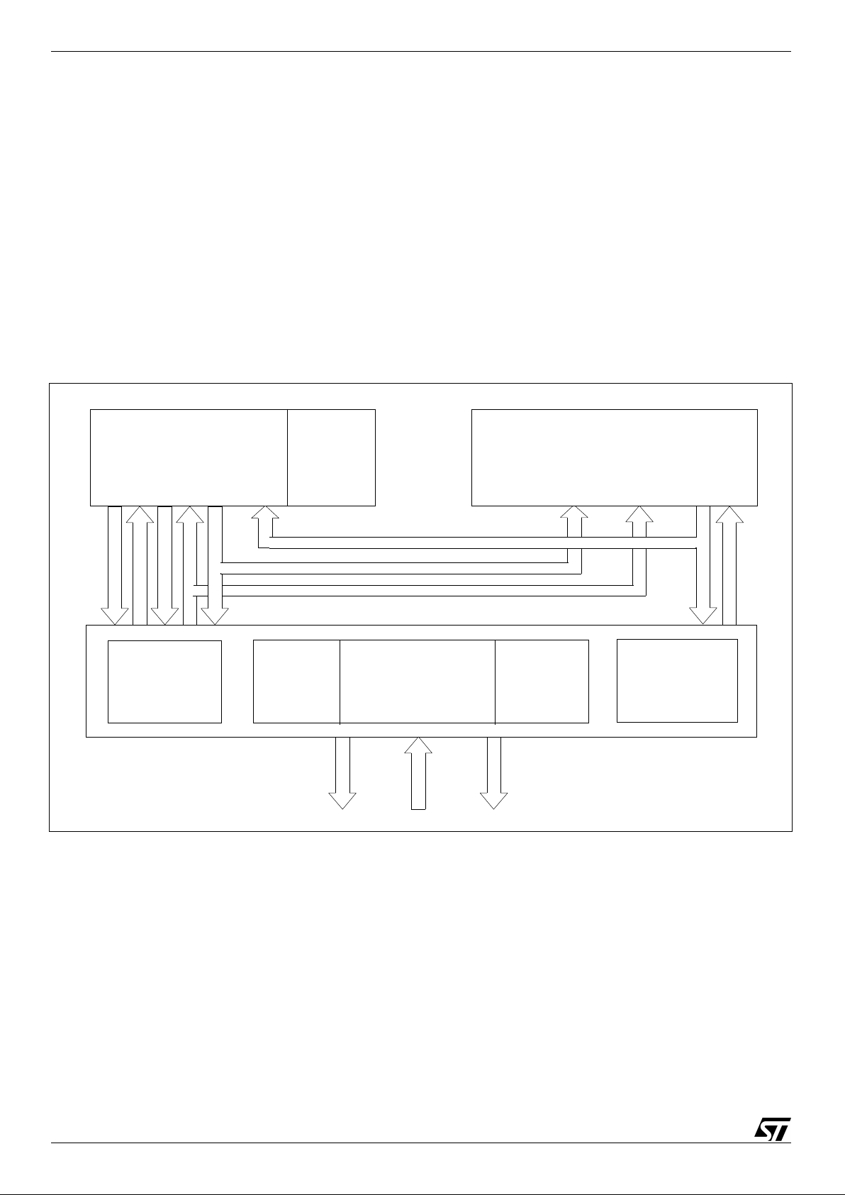
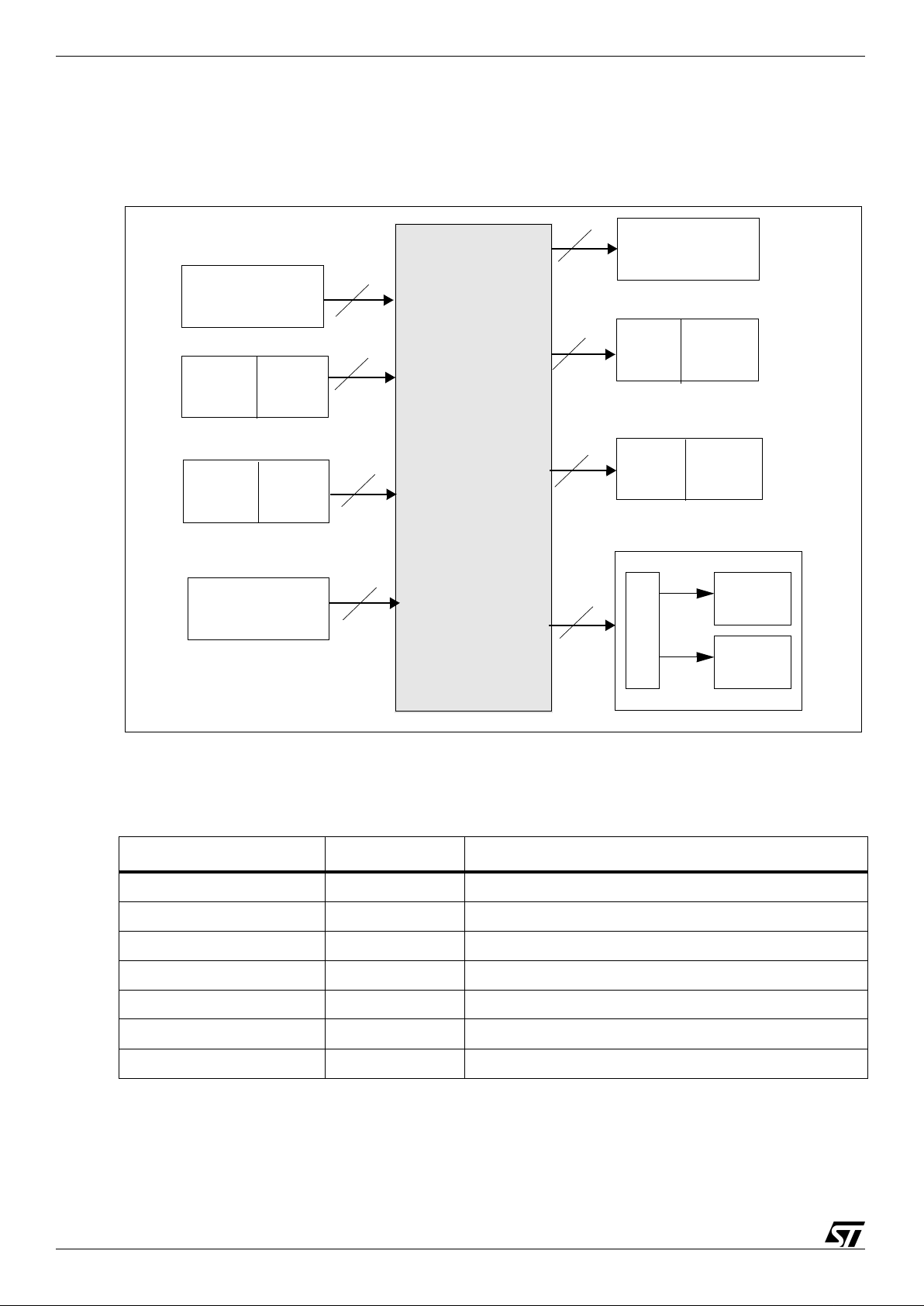
The architecture of the SuperHyway interconnect is shown in
Figure 3
. Initiato rs are shown on t he
left, and targets are shown on the right of the interconnect. The bit width of the initiator and target
ports are s how n in the diag ram.
The ST4 0R A architec t ure requires se v en memory bridges on cloc k c hange boundaries.
Figure 3: ST40RA interconnect architecture
Memory bridge number SuperHyway type Subsystem
1 T3 EMI target
2 T3 EMPI initiator
3 T1 EMI_SS target
4 T2 Reserved
5 T2 Reserved
6T3PCI_ST_I
7T3PCI_ST_T
Table 9: Memo ry bridges
SuperHyway
Interconnect
SH core
EMPI
PCI_ST_I
LMI
EMI
PCI_ST_T
Memory
bridge
Memory
bridge
Memory
bridge
Memory
bridge
P
I
PER
SH_PER
32
32
32
GPDMA
32
64
32
32
32
Page 22
ADCS 7260755H STMicroelectronics 22/94
ST40RA
5 Syst
em configuration
5.8.1 Memory bridge control signals
Each me m ory bridge has s ev en control s ignals as def ined in
Table 10
.
5.8.2 Memory bridge status
The memory bridge control signals are looped back to the ST40RA comms subsystem SYS_STAT1
registe r fo r t es t purposes. The format o f this read-only register is show n in
Section 5.9.4.1:
SYSCONF.SYS_STAT1. on page 26
.
5.8.3 Changing control of a memory bridge
At reset all these bridges are set to be synchronous. After reset and boot the function of these
memor y bridges can be changed . See
Section 5.9.4: SYSCONF registers on page 26
. The
procedure for changing the control of a me m ory bridge is g iv en below.
1 Ensure no init iat ors are acc es s ing the subs yst em the bridge is connec t ed to and ensure the
subsystem cannot init iate any requests to the SuperHyway.
2 Stop the clock to the subsystem.
3 Change the memory bridge configuration using the SYS_CONF.SYS_CON1 register as
detailed in
Table 10
.
4 Restart the clock to the subsystem and reinitialize the system.
Bridge control bit field Control name Control function
1:0 MODE[1:0] 00: Sync (bypass) bridge
01: Semisync with no retime registers
10: Semisync with one ret ime register
11: Async with two retime registers
4:2 LATENCY[2:0] Sets FIFO latency from 0 to 7 cycles.
5 SW_RESET 0: Software reset inactive
1: Software reset active
6 STROBE The above control signals are latched in the bridge on the rising
edge of this strobe bit
Tab le 10: Memory b rid ge co ntrol signal s
Page 23
5 Syst
em configuration
ST40RA
23/94 STMicroel ec tronics ADCS 7260755H
5.9 System configuration registers
Table 11
outlines the ST40RA system configuration registers.
Register Module
Address
offset
Type Description
EMI.GENCFG EMI 0x028 R/W EMI general purpose configuration register, see
Section 5.9.1: EMI.GENCFG EMI gener al
configuration on page24
LMI.COC LMI 0x028 R/W LMI clock and pad control register, see
Section 5.9.2: LMI.COC on page 25
LMI.CIC LMI 0x040 RO LMI clock and pad status, see
Section5.9.3:
LMI.CIC on page 26
SYS_STAT1 SYSCONF 0x040 RO Memory bridge status , see
Section 5.9.4.1:
SYSCONF.SYS_STAT1. on page 26
SYSCONF.SYS_CON1 SYSCONF 0x010 R/W System configuration register, see
Section 5.9.4.2: SYSCONF.SYS_CON1. on
page 27
SYSCONF.SYS_CON2 SYSCONF 0x018 R/W System configuration register, see
Section 5.9.5:
SYSCONF.SYS_CON2. on page 27
SYSCONF.CNV_STATUS SYSCONF 0x020 R/W System configuration register, see
ST40 System
Architecture Manual Volume 4: I/O Devices
SYSCONF.CNV_SET SYSCONF 0x028 R/W System configuration register, see
ST40 System
Architecture Manual Volume 4: I/O Devices
SYSCONF.CNV_CLEAR SYSCONF 0x030 R/W System configuration register, see
ST40 System
Architecture Manual Volume 4: I/O Devices
SYSCONF.CNV_CONTROL SYSCONF 0x038 R/W System configuration register, see
ST40 System
Architecture Manual Volume 4: I/O Devices
Table 1 1: System configuration registers
Page 24
ADCS 7260755H STMicroelectronics 24/94
ST40RA
5 Syst
em configuration
5.9.1 EMI.GENCFG EMI general configuration
EMI.GENCFG EMI general configuration 0x0028
The EM I pr ov ides a gene ric register to al low t he configuration of the padlogic. ST 40RA
uses the bits detaile d.
0SOFE Strobe positioning
Strobe on falling edge:
0: Disabled
1: Enabled
Rese t: 0
RW
[5:1] SDPOS SDRAM bank location
00001: Bank 0 00010: Bank 1
0001 1: Bank 2 00100: Bank 3
00101: Bank 4 00110: Bank 5
10001: Bank 0 to 1 10010: Bank 0 to 2
1001 1: Bank 0 to 3 10100: Bank 0 to 4
10101: Bank 0 to 5 10110: Bank 1 to 2
101 11: Bank 1 to 3 11000: Bank 1 to 4
1 1001: Bank 1 to 5
11010: Ba nk 2 t o 3
1 1011: Bank 2 to 4 1110 0: Bank 2 to 5
1 1101: Bank 3 to 4 11110: Bank 3 to 5
11111: Bank 4 to 5
Rese t: 0
RW
6EWPU
Pull-up on EWAI T pin
a
0: Disabled
1: Enabled
Rese t: 0
a. If the EWAIT signal is set at the beginning of an access, and the data is to be set after the EWAIT
is cleared, the parameters ACCESSTIMEREAD and LATCHPOINT in the EMI configuration
registers must be set as follows:
ACCESSTIME > LATCHPOINT + 3.
See the
ST40 System Architecture Manual, Volume 2: Bus Interfaces
for details of setting the EMI
configuration registers.
RW
7 EAPU Pull-up enable on EADDR pins
0: Disabled
1: Enabled
Rese t: 0
RW
[31:8] Reserved 0: Ignored
1: Reserved
Reset: Undefined
Page 25
5 Syst
em configuration
ST40RA
25/94 STMicroel ec tronics ADCS 7260755H
5.9.2 LMI.COC
LMI.COC LM I cl ock and pad control 0x028
LMI.COC allows modific ati on of the glue logic.
0 DLY_SRC Delay line control source
0: DLL provides delay line control
1: LMI.CFG[5:1] provides delay line control
Rese t: 0
RW
[5:1] DLY_NUM Number of delays (~200ps each)
Rese t: 0
RW
[7:6] DLY_FRQ_RES External delay frequency resolution
Rese t: 0
RW
19:8] PLL_SETUP PLL setup
Rese t: 0
RW
[21:20] DLL_PRO_CON DLL programmer control
Rese t: 0
RW
22 FRQ_RES_SRC Frequency resolution source of external delay
0: DLL provides frequency resolution
1: LMI.CFG[7:6] provides frequency resolution
Rese t: 0
RW
23 PLL_SETUP PLL setup
Rese t: 0
RW
24 DLL_PRO_SRC DLL programmer source
0: Delay programmer bl ock provides DLL programming
1: LMI.CFG[21:20] provides DLL programming
Rese t: 0
RW
[30:25] Reserved
31 DLL_ENB DLL enable
Rese t: 0
RW
Page 26
ADCS 7260755H STMicroelectronics 26/94
ST40RA
5 Syst
em configuration
5.9.3 LMI.CIC
5.9.4 SYSCONF registers
All ST40 systems contain a number of general purpos e configurat ion registers which may be used
to configure system logic.
The def init ion of the general regis te rs and their acc es s fu nc t ions is defin ed in the
ST40 System
Architecture Manual.
For ST4 0R A the bits wit hin these regis t ers have th e fo llowing func t ion.
5.9.4.1 SYSCONF.SYS_STAT1.
LMI.CIC LMI clock and pad status
0x040
LMI.CIC reflects the status of the glue logic.
[4:0] DLY_STATE DLL delay state RO
5 DLL_LOCK DLL lock signal RO
6 PLL_LOCK PLL lock signal RO
[8:7] DLL_STATE DLL state RO
[21:9] PLL_SETUP_STATE PLL setup state RO
[24:22] DLL_SETUP_STATE DLL setup state RO
[26:25] DLL_BYPASS DLL bypass state RO
[31:27] LMI_SETUP LMI.CFG setup for external delay RO
SYS_STAT1 Memory bridge status 0x0040
[3:0] Reserved
[10:4] STATUS1 Status memory bridge 1 RO
[17:11] STATUS2 Status memory bridge 2 RO
[24:18] STATUS3 Status memory bridge 3 RO
[31:25] STATUS4 Status memory bridge 4 RO
[38:32] STATUS5 Status memory bridge 5 RO
[45:39] STATUS6 Status memory bridge 6 RO
[52:46] STATUS7 Status memory bridge 7 RO
[63:53] Reserved
Page 27
5 Syst
em configuration
ST40RA
27/94 STMicroel ec tronics ADCS 7260755H
5.9.4.2 SYSCONF.SYS_CON1.
Where the two clocks are sourced from independent PLLs the br idge must be put in asynch ronous
mode.
5.9.5 SYSCONF.SYS_CON2.
SYSCONF.SYS_CON1 Memory bridge control 0x010
[3:0] Reserved RW
[10:4] MB1 Memory bridge 1 control: EMI target RW
[17:11] MB2 Memory bridge 2 control: EMPI initiator RW
[24:18] MB3 Memory bridge 3 control: EMI_SS target RW
[38:25] Reserved
[45:39] MB6 Memory bridge 6 control: PCI initiator RW
[52:46] MB7 Memory bridge 7 control: PCI target RW
[63:53] Reserved
SYSCONF.SYS_CON2 Functional pin use and behavior 0x0018
The SYSCONF.SYS_CON2 register controls functional pin use and behavior
8LMI_MODE
LMI pad type
0: SSTL
1: LVTTL
Reset: 0
RW
9 LMI_ENVREF
Reference voltage source
0: internally generated reference voltage
1: external reference voltage from VREF pins
Reset: 0
RW
10 LMI_ECLK_BYPASS
LMI control signal ECLK180 retime bypass
0: ECLK180 flip flop not by passed
1: ECLK180 flip flop is bypassed
Reset: 0
RW
11 LMI_NOTCOMP25_EN
Enable LMI 2.5 V compensation cell
0: LMI 2.5 V compensation cell enabled
1: LMI 2.5 V compensation cell disabled
Reset: 0
RW
12 LMI_COMP33_EN
Enable LMI 3.3 V compensation cell
0: LMI 2.5 V compensation cell enabled
1: LMI 2.5 V compensation cell disabled
Reset: 0
RW
Page 28

ADCS 7260755H STMicroelectronics 28/94
ST40RA
5 Syst
em configuration
[13:14] LMI _SDRAM_DATA_DRIVE
SDRAM data and data strobe pad PROG 1:0 L VTTL
OP drive strength
00: 1x
01: 2x
10: 3x
11 : 4x
Reset: 0
RW
[15:16] LMI _SDRAM_ADD_DRIVE
LMI address and control pad PROG 1:0 LVTTL OP
drive strength
00: 1x
01: 2x
10: 3x
11 : 4x
Reset: 0
RW
[17:35] Reserved
36 EMPI_ENB[0]
Enable EMPI channel 0 DREQ/DRACK/DRACK
alternate function
0: Disabled
1: NOTESCS1 remapped to EMPIDREQ0
NOTESCS2 remapped to EMPIDRAK0
EADDR26 remapped to EMPIDACK0
EADDR26 is only remapped when whilst the ST40RA
is acting as a bus slave
RW
37 EMPI_ENB[1]
Enable EMPI channel 1 DREQ/DRACK/DRACK
alternate function
0: Disabled
1: NOTPREQ3 remapped to EMPIDREQ1
NOTPGNT3 remapped to EMPIDRAK1
EADDR25 remapped to EMPIDACK0
EADDR25 is only remapped when whilst the ST40RA
is acting as a bus sla ve
RW
38 EMPI_ENB[2]
Enable EMPI channel 2 DREQ/DRACK/DRACK
alternate function
0: Disabled
1: DREQ0 remapped to EMPIDREQ2
DACK0 remapped to EMPIDACK2
DRAK0 remapped to EMPIDRAK2
RW
39 EMPI_ENB[3]
Enable EMPI channel 2 DREQ/DRACK/DRACK
alternate function
0: Disabled
1: DREQ1 remapped to EMPIDREQ3
DACK1 remapped to EMPIDACK3
DRAK1 remapped to EMPIDRAK3
RW
40 MAILBOX_ENB
Enable mailbox interrupt alternate function
0:Disabled
1:NOTESC0 remapped to MBXINT
RW
[41:43] R eserved
SYSCONF.SYS_CON2 Functional pin use and behavior 0x0018
Page 29
5 Syst
em configuration
ST40RA
29/94 STMicroel ec tronics ADCS 7260755H
5.9.6 PIO alternate functions
The fun ction of pads w it h PI O alternate function s are c ontrolled by th e PI O.PC0, PIO.PC1 and
PIO.PC2 registers .
In the ST40RA devic e, the operat ional mod es fo r t hes e registers differ from the st andard
archite c tu re definition and are sho w n in
Table 12
.
[44:46] EM PI_CS_ENB
Enable EMPI chip selection alternate function
000: NOTESC0 remapped to NOTEMPICS
001: NOTESC1 remapped to NOTEMPICS
010: NOTESC2 remapped to NOTEMPICS
011: NOTESC3 remapped to NOTEMPICS
100: NOTESC4 remapped to NOTEMPICS
101: NOTESC5 remapped to NOTEMPICS
110: Reserved
1 11: Disabled (val ue at reset)
RW
47 SEL_EXT_EMI_SLAVE
Select EMI slave or master functionality
0: EMI is bus master
1: EMI is bus slave
RW
[48:59] Reserved
[60:63] PIO_CONF PIO_CONF RW
PIO bi t configur a tion PIO out put state PI O.PC2 PIO.PC 1 PIO.PC0
NonPIO function
a
a. State following reset
-000
PIO bidirectional Open drai n 0 0 1
PIO output Push-pull 0 1 0
PIO bidirectional Open drai n 0 1 1
PIO input Hi gh impedance 1 0 0
PIO input Hi gh impedance 1 0 1
Reserved - 1 1 0
Reserved - 1 1 1
Table 12: PIO alternate function registers
SYSCONF.SYS_CON2 Functional pin use and behavior 0x0018
Page 30

ADCS 7260755H STMicroelectronics 30/94
ST40RA
6 Clock
generation
5.9.7 PCI.PERF register definition.
6 Clock generation
The ST4 0 c lock architec t ure has bee n organize d to m aintain com patibility across the ST40 family
and allow additional flexibility to increase system performance where required. It includes a more
diverse range of peripherals and provides low power use.
6.1 Clock domains and sources
Figure 4
shows possible clock domains for ST40RA clocks. The ST40RA implementation includes
two CLOCKGEN macros, which supply up to three independent clock domains across the chip
Each PLL may be independently programmed to p roduce a cloc k at a sp ec if ic f requency w hic h is
used to d eriv e a series of related cloc ks w hich may be us ed by the system.
The clock domains m apping is shown in
Table 13
. The architectur e of the ST40RA CLOCKGEN
subsystem consists of two standard (ST40 family) CLOCKGEN units (CLOCKGENA and
CLOCKGENB) and a CLOCKCON block.
Figure 5
shows th e architecture of the ST 40R A
CLOCKGEN subsystem.
PCI.PERF 0x0080
PCI.PERF modifies the function of the PCI.
[3:0] DLY_PERRSAMPLE Parity error delay
Number of APP_CLOCK cycles after end of PCI that access master
should wait to see if there is a parity err or
RW
4 ENB_WRITEPOST Enable write posting in master RW
5 ENB_STBYBYPASS Enable standby bypass RW
[31:6] Reserved
Page 31

6 Clock
generation
ST40RA
31/94 STMicroel ec tronics ADCS 7260755H
Figure 4: ST40RA clock domains
SuperHyway
CPU_CLK
PER_CLK
LMI_CLK
EMI_SS_CLK
CLOCKGEN
PCI_SS_CLK
PCI_BUS_CLK
XTAL
(X_IC K)
SH-4 CPU
SH-4 core
(X_PCK)
(X_BCK)
LMI
SDRAM
DLL
Flash
.
PCI
subsystem
or DDR
CLK
CLK
subsystem
PCI int.
CLK
PCI
bus
EMI
subsystem
LMI int
STBUS_CLK
STBUS_CLK
memory
MPX bus
,
SDRAM
See CLOCKGENA.PLL1 clock domains
See CLOCKGENA.PLL2 clock domains
See CLOCKGENB.PLL1 clock domains
peripherals
core
(X_PCK)
27 MHz
Page 32

ADCS 7260755H STMicroelectronics 32/94
ST40RA
6 Clock
generation
The sources for PCI_SS_CLK and EMI_SS_CLK, can be set using the PCI_SEL and EMI_SEL bits
in the CLOCKGENB.CLK_SELCR register. See
Secti on 6.6.1: CL OCKG ENB .C LK_ SEL CR r e gis t er
on page 39
.
If CLOC KGEN_A1 3 is us ed as PCI_ SS_CLK source then t he m emory bridges 6 and 7 m us t be
enable d. If C LOCKGE N _A12 is used, t hen the bridg es m ay be placed in by pass mode . Th is is the
recommended m ode of opera ti on.
If either CLOCKGEN_B12 or CLOCKGEN_A14 are used as the EMI_CLK, the memory bridges 1, 2
and 3 mus t be enabled. If C LOCKGEN_A12 is used, then th e bridges may be placed in by pass.
This is the rec ommended mode o f op eration.
See
Chapt er 5.8: Mem ory bridge control on pa ge 21
.
Subsystem Clock domain
Target frequencies
(MHz)
Source
a
Ratio
CPU core CPU_CLK 200 166 150 133 CLOCKGEN_A11 1
SuperHyway STBUS_CLK - 111 100 88 CLOCKGEN_A12 2/3
100 83 75 67 1/2
Peripherals PER_CLK
(CPU core PCK)
- 555044CLOCKGEN_A13 1/3
50 42 38 33 1/4
PCI bus clock PCI_BUS_CLK 33 CLOCKGEN_A21 1/16
66 CLOCKGEN_A2 2 1/8
25.14 CLOCKGEN_A23 1/21
Disabled CLOCKGEN_A24 -
PCI subsystem PCI_SS_CLK - 111 100 88 CLOCKGEN_A12 2/3
100 83 75 67 1/2
- 555044CLOCKGEN_A13 1/3
50 42 38 33 1/4
Local memory
interface (LMI)
LMI_CLK 133 111 100 88 CLOCKGEN_A14 2/3
Reserved CLOCKGEN_B11 1
EMI subsystem EMI_CLK 50 to 100 MHz CLOCKGEN_B12 1
- 111 100 88 CLOCKGEN_A12 2/3
100 83 75 67 CLOCKGEN_A14 1/2
Table 13: Clock domains
a. Clock naming: CLOCKGEN_[CLOCKGEN label][PLL number][clock number]
Page 33

6 Clock
generation
ST40RA
33/94 STMicroel ec tronics ADCS 7260755H
Figure 5: ST40RA CLOCKGEN subsystem
27 MHz
1
2
3
4
ST40 CLOCKGENA
PLL2
PLL1
LPU
Control
Control
ST40 CLOCKGENB
CPU_CLK (X_ICK)
STBUS_CLK (X_BCK)
PER_CLK (X_PCK))
LMI_CLK
EMI_SS_CLK
ST40RA CLOCKGEN subsyste m
CLOCKCON
PLL1
PLL2
PCI_SS_CLK
PCI_BUS_CLK
CLK_SEL[3:0]
XTAL
CPU core
SuperHyway
T1
ST40RA
1
2
3
4
5
1
2
3
4
PLL1
LPU
Control
PLL1
T1
0
1
00
01
10
11
0
1
PCI_SEL
EMI_SEL
LMI_SEL
Select
(external)
Control
PLL2
1
2
3
4
5
Page 34

ADCS 7260755H STMicroelectronics 34/94
ST40RA
6 Clock
generation
6.2 Recommended operating modes
6.3 Clocks and registers at start up
Mode for
CLOCKGENA and
CLOCKGENB
PLL
frequency
(MHz)
ST40RA clock domain frequencies (MHz)
PLLA
(mode)
PLLB
(mode)
PLLA PLLB
CPU_
CLK
STBUS_
CLK
PER_
CLK
LMI_
CLK
EMI_SS_
CLK
PCI_SS_
CLK
Recommended reset con figuration
0 - 200 - 100 50 25 50 50 50
Alternate reset configuration
1 - 266 - 133 88 44 88 88 88
2 - 300 - 150 100 50 100 100 100
3 - 332 - 166 111 66 111 111 111
Recommended operating m odes
2 - 300 - 150 100 100 100 100 100
3 - 332 - 166 83 83 83 83 83
Low power configuration with clocks enabled (programmable after reset )
A6
bypass
- 27 - 13.5 6.75 6.75 6.75 6.75 6.75
Table 14: Supported operating frequencies
Reset
mode
Reset
mode
MODE[2:0]
CLOCKGENA
.PLL1CR1
reset value
CLOCKGENA
core
frequency
(PLL1)
f
PLL
/2
CLK1
CPU_
CLK
CLK2
STBUS_
CLK
CLK3
PER_
CLK
CLK4
LMI_
CLK
0 000 0x7939 8612 200 MHz 100 1 1/2 1/4 1/2
1 001 0x7939 B112 266 MHz 133 1 2/3 1/3 2/3
2 010 0x7938 6412 300 MHz 150 1 2/3 1/3 2/3
3 01 1 0x7938 7B14 332 MHz 166 1 2/3 1/3 2/3
4 100 0x7938 8612 400 MHz 200 1 1/2 1/4 1/2
5 101 0x7938 A712 500 MHz 250 1 1/2 1/4 1/2
6 110 0x0938 0000 0 MHz 0 1 1/2 1/2 1/2
7 111 0x0939 861 2 200 MHz 100 1/2 1/4 1/4 1/4
Table 15: CLOCKGENA PLL1 reset values
Page 35

6 Clock
generation
ST40RA
35/94 STMicroel ec tronics ADCS 7260755H
6.3.1 CLOCKGENA_2x PCI (P CI_DIV_BYPASS = 0)
6.3.2 Division ratios on CLOCKGENA_2x
Reset mode
MODE[4:3]
Reset value PLL2 frequency
00 0x7938 B012 528 MHz
01 0x7938 B012 528 MHz
10 0x7938 B012 528 MHz
1 1 0x0938 B012 0 MHz
Table 16: CLOCKG E NA PLL2 reset values (PCI_DIV_BYPASS = 0)
Mode
MODE[4:3]
Divide ratio selected PCI_BUS_CLK freq.
00 8 66 MHz
01 16 33 MHz
10 21 25.14 MHz
11 - 0 MHz
Table 17: CLOCKGENA_PLL2 PCI reset division ratios.
Page 36

ADCS 7260755H STMicroelectronics 36/94
ST40RA
6 Clock
generation
6.4 Setting clock frequencies
Table 18
shows valid FRQCR ratios and the associated clock frequencies for derived clocks.
CLOCKGENA.FRQCR and
CLOCKGENB.FRQCR
ST40RA codified ratios Clock ratios
Lower 9 bit
Available
on start up
CPU_
CLK
BUS_
CLK
PER_
CLK
CPU_
CLK
BUS_
CLK
PER_
CLK
0x000
11
1/2 1 1 1/2
0x002 1/4 1 1 1/4
0x004 1/8 1 1 1/8
0x008 MODE6
1
1/2
1/2 1 1/2 1/2
0x00A MODE[4:5] 1/4 1 1/2 1/4
0x00C 1/2 1/8 1 1/2 1/8
0x011 2/3 1/6 1 2/3 1/6
0x013 MODE[2:3]
1
2/3 1/3 1 2/3 1/3
0x01A MODE0 1/2 1/4 1 1/2 1/4
0x01C 1/8 1
1/2 1/8
0x023 MODE1 1 2/3 1/3 1 2/3 1/3
0x02C 1/2 1/8 1 1/2 1/8
0x048
1/2
1/2
1/4 1 1 1/2
0x04A 1/6 1 1 1/3
0x04C 1/8 1 1 1/4
0x05A
1/3 1/6 1 2/3 1/6
0x05C
0x063 MODE7 1/2 1/4 1/4 1 1/2 1/2
0x06C 1/2 1/8 1 1/2 1/4
0x091
1/3
1/3
1/6
111/2
0x093
0x0A3 1/6 1 1/2 1/2
0x0DA
1/4
1/4
1/8
111/2
0x0DC
0x0EC 1/8 1 1/2 1/2
0x123 1/4 1 1 1/2
0x16C 1/8 1 1/2 1/2
Table 18: Valid FRQCR values and their ratios
Page 37

6 Clock
generation
ST40RA
37/94 STMicroel ec tronics ADCS 7260755H
6.4.1 Programming the PLL output frequency
The three dividers used within the PLL are referred to as M (predivider), N (feedback divider) and P
(postdivider) for brevity . Note that there is a divide-by-2 fixed prescaler before the feedback divider.
The binary values applied to the programmable divid ers , and the frequency of CLOCKIN controls
the outp ut fr equency of the PLL macroc ell:
where th e v alues of M, N and P must sat is fy t he following c onstraint s :
● Divider limits: ,
● Phase comparator limits: ,
● VCO limit : ,
● M divid er limit: .
For example, if 300 MHz from an input clock of 33 MHz is to be generated, the values of M, N and
P are work ed out as below.
1 The phase comparator must operate between 1 MHz and 2 MHz, so choose M = 22 (for
1.5 MHz operation).
2 The VCO needs to run between 200 MHz and 622 MHz. It could be ru n at 300 MHz directly
(which takes a little less current), or at 600 MHz then divide by 2 to ensure an e xact 50% duty
cycle. In this example 600 MHz is chosen so N = 200.
3 The postdivi der then nee ds to be a divide by 2. T his is programmed in powe rs of 2, so P = 1.
The P div ider change s va lue without glit c hing of the out put clock.
6.4.2 Changing clock frequency
The clock frequencies are changed in two ways.
● Chang e t he core PLL frequencie s .
The PLL must be stopped, the control register reconfigured with the new settings, and the PLL
restarted at the new frequency.
● Change the frequency division ratio of the clock domains.
The control registers are change d dy namically and the new f requencie s are effective
immedia t ely.
6.4.3 Changing the core PLL frequencies
This pro c edure applies t o either CLOC KGENA or C LOCKGE N B and to PLL1 or PLL2.
1 Stop the PLL. The CLO C KGENA.PLL1CR2. ST BPLLEN SEL register selects w hether the PLL
is enabled by the CLO C KGENA.PLL1CR2. STBPLLE N or the CPG. FRQCR.PLL1EN register.
2 Rec onfigure th e PLL. Set the CL OCKGENA.PLL1CR1 regist er t o one of the su pported
configur at ions on the dat asheet.
3 Restart the PLL, following the procedure described in the
ST40 System Architecture Volume 1:
System
.
F c lockout()
2N×
M2
P
×
------------------ F c l o c k i n()×=
1 M 255 1 N 255 0 P 5≤≤,≤≤,≤≤
1MHz
F clockin()
M
-----------------------------
2MHz≤≤
200MHz
2N×
M
-------------
F clockin()× 622MHz≤≤
F c lockin()200MHz
·
≤
Page 38

ADCS 7260755H STMicroelectronics 38/94
ST40RA
6 Clock
generation
6.4.4 Changing the frequency division ratio
The frequency division ratio is selected by changing the CPG.FRQCR register for PLL1 or the
CLOCK GENA.PLL2_MUXCR regis te r fo r PLL2. This ch ange is imme diately effectiv e.
6.5 Power management
The power management unit (PMU) is responsible for clock startup and shutdown for each of the
on-chip m odules. Power is con se rv ed by powering down th os e m odules whic h are not in u se , or
even the CPU itself.
The PM U is o perated using three ba nk s of registers as f ollows:
● CPG: controls the power-down mode of th e C PU and the power-do w n s t at es of th e legacy
on-chip peripherals ,
● CLOC KGENA and CLOCKGENB: control th e power-do w n s t at es of t he other on-chip peripherals.
6.5.1 CPU low-power modes
The CPU can be put into sleep or standby modes. In sleep mode the CPU is halted while the
on-chip peripherals continu e t o operate. In standby mode all the on -c hip peripherals are sto pped
along wit h t he CPU. In addition, the on-chip per ipherals can be independently stopped.
Power down is initiated with the sleep instruction and the power down mode is selected with bit 7 of
the CPG.STBCR register. If the bit is set, the CPU enters standby mode on the ne xt sleep
instruction, and if unset it enters sleep mode.
6.5.2 Module low-power modes
Modules are powered down in two ways, depending on whether the module is a ST40 legacy
periph eral (controlled by the CP G register bank) or a ST40RA peri pheral (con tro lled by the
CLOCKGEN register banks).
A module controlled by the CP G register bank has its clo c k stopped whe n t he corresponding bit in
the CPG.STBCR or CPG.STBCR2 registe r i s set. The clock is starte d again wh en th e bit is cleared.
To reques t th e power down of a module controlled by the CL OC KGENA or C LOCKGE N B register
bank, 1 is w rit t en to the corr es ponding bit in t he
STBREQCR _SET reg is te r. When th e m odule has
comple t ed it s power down s equence and its clock ha s been stopped, the corr es ponding bit in t he
STBAC KC R registe r is se t. To restart the module, 1 is writte n t o t he c orrespon ding bit in the
STBREQCR_CLR register .
Note: The modules governed by the
CLOCKGENB
register bank do not support hardware-only power down
and req uire software interacti on t o m aintain da ta c oherency bef ore mak ing a request t o s to p t he
module c lock.
6.6 Clock generation registers
Page 39

6 Clock
generation
ST40RA
39/94 STMicroel ec tronics ADCS 7260755H
6.6.1 CLOCKGENB.CLK_SELCR register
CLOCKGENB.CLK_SELCR Clock source selection 0x0068
The CLKGENB.CLK_SELCR register con trols the selection of clock domain clock sources
0 LMI_SEL
Reserved
Reset state: 0
1 PCI_SEL
Select PCI clock
0: PCI_SS_CLK from CLOCKGENA_12
1: PCI_SS_CLK from CLOCKGENA_13
Reset state: 0
RW
[2:3] EMI_SEL
Select EMI clock
00: EMI_SS_CLK from CLOCKGENA_12
01: EMI_SS_CLK from CLOCKGENA_13
10: EMI_SS_CLK from CLOCKGENA_14
11: EMI_SS_CLK from CLOCKGENB_12
Res e t state : 00
RW
[4:7] EXT_CLK_SEL
Not used
Reset state: 0000
[8:31] R eserved Reset state: 0 RW
Page 40

ADCS 7260755H STMicroelectronics 40/94
ST40RA
6 Clock
generation
6.6.2 CPG.STBCR register
CPG.STBCR Sleep or standby mode 0x0004
Select between sleep and standby modes when a sleep instruction is issued.
0 MSTP0
SCIF1 standby
0: SCIF1 operates
1: SCIF1 clock stopped
Reset state: 0
RW
1 MSTP1
RTC standby
0: RTC operates
1: RTC clock stopped
Reset state: 0
RW
2 MSTP2
TMU standby
0: TMU operates
1: TMU clock stopped
Reset state: 0
RW
3 MSTP3
SCIF2 standby
0: SCIF2 operates
1: SCIF2 clock stopped
Reset state: 0
RW
4 MSTP4
Not used
Reset state: 0
RW
5 PPU
Peripheral module pull-up pin control
Controls the state of per ipheral mod ule rel ated pins
in the high impedance state
0: Peripheral module rel ated pin pull-up resistors
are on
1: Peripheral module rel ated pin pull-up resistors
are off
Reset state: 0
RW
6PHZ
Peripheral module pin high impedance control
Controls the state of per ipheral mod ule rel ated pins
in standby mode
0: Peripheral module rel ated pins are in normal
state
1: Peripheral module rel ated pins go to high
impedance state
Reset state: 0
RW
7STBY
Standby
0: Transit ion to sleep mode on sleep instruction
1: Transition to standby mode on sleep instruction
Reset state: 0
RW
Page 41

6 Clock
generation
ST40RA
41/94 STMicroel ec tronics ADCS 7260755H
6.6.3 CLOCKGENA.STBREQCR and CLOCKGENB.STBREQCR registers
6.6.4 CLOCKGENA.STBREQCR_SET and CLOCKGENB.STBREQCR_SET registers
6.6.5 CLOCKGENA.STBREQCR_CLR and CLOCKGENB.STBREQCR_CLR register
CLOCKGENA.STBREQCR
CLOCKGENB.STBREQCR
Control power down requests 0x0018
This regist er gi ves direct access to the power down request regi ster. Low power request s are made in
the STBREQCR_SET register and cleared in the STBREQCR_CLR register.
[0:7] REQ[0:7]
Power down requests for module [n]
Controls the power down state for module [n]
Bit [n]: 0 Request module [n] to operate normally
Bit [n]: 1 Request module [n] to power down
Reset state: 0
RW
[8:31] Reserved
0: No action
1: Undefined
Reset state: Undefined
CLOCKGENA.STBREQCR_SET
CLOCKGENB.STBREQCR_SET
Set power down reque sts 0x0020
This register sets a low power request.
[0:7] SET[0:7]
Set power down request for module [n]
Sets the power down request state for module [n]
Bit [n]: 0 No action
Bit [n]: 1 Set power down request
Reset state: 0
WO
[8:31] R eserved
0: No action
1: Undefined
Reset state: Undefined
CLOCKGENA.STBREQCR_CLR
CLOCKGENB.STBREQCR_CLR
Clear power down requests 0x0028
This register clears a low power request and recommences the clock supply to a module.
[0:7] CLR[0:7]
Clear power down request for module [n]
Clears the power down request state for module [n]
Bit [n]: 0 No action
Bit [n]: 1 Clear power down request
Reset state: 0
WO
[8:31] Reserved
0: No ac tion
1: Undefined
Reset state: Undefined
Page 42

ADCS 7260755H STMicroelectronics 42/94
ST40RA
6 Clock
generation
6.6.6 CLOCKGENA.STBACKCR and CLOCKGENB.STBACKCR register
Table 19
defines the m apping of modules to bit s in th e STBREQ and STBACK registers.
CLOCKGENA.STBACKCR
CLOCKGENB.STBACKCR
Current module power status 0x0030
This register indicates the current module power status
[0:7] ACK[0:7]
Power down status for module [n]
Indicates the current power down status of the
module [n]
Bit [n]: 0 Module [n] oper ati ng normally
Bit [n]: 1 Module [n] powered down
Reset state: 0
RO
[8:31] R eserved
0: No action
1: Undefined
Reset state: Undefined
Bit number
CLOCKGENA
mapping
CLOCKGENB
mapping
0EMIReserved
1LMIReserved
2 DMAC Reserved
3 PCI Reserved
4PIOReserved
5 Reserved Reserved
6 Reserved PCI bus
7 Reserved Reserved
Tab le 19: STBREQ and STBACK mapping for modules
Page 43

7 Electrical
spec
ificati
ons
ST40RA
43/94 STMicroel ec tronics ADCS 7260755H
7 Electrical specifications
7.1 DC ab so lu te ma xi mu m rat ing s
7.1.1 Fmax clock domains
Symbol Parameter Min Max Units Notes
VDDCORE Core DC supply voltage 2.1 V
a,b
a. Stresses greate r than those listed under
Table 20: Absolute ma ximum ratings
may cause
permanent damage to the device. This is a stress rating only and functional operation of the device
at these or any other conditions above those indicated in the operating sections of this specification
is not implied. Exposure to absolute maximum rating conditions for extended period may effect
reliabilit y.
b. All I/O pins are 3.3 V tolerant except CLKIN, LPCLKIN, CLKOSC and LPCLKOS C.
VDDIO I/O DC supply voltage 4.0 V
VDD
RTC RTC DC supply voltage 2.1 V
V
IO Vol tage on input, output and bi directional pins. GND -0.6 VDDIO + 0.6 V
V
IORTC Voltage on input pins on VDDRTC supply
(LPCLKIN, LPCLKOSC)
GND -0.6 VDDRTC + 0.6 V
VIO
CLK
Voltage on CLKIN and CLKOSC pins GND -0.6 VDDCORE + 0.6 V
I
O DC output current 25 mA
T
S Storage temperature (ambient) -55 125 deg C
T
A Temperature under bias (ambient) -55 125 deg C
Table 20: Absolute maximum ratings
Function clock ST40RA200XH6 ST40RA166XH6 ST40RA150XH6
CPU_CLK 200 MHz 166 MHz 150 MHz
STBUS_CLK 100 MHz 111 MHz 100 MHz
PER_CLK 50 MHz 55 MHz 50 MHz
LMI_CLK 133 MHz 100 MHz 100 MHz
EMI_SS_CLK 100 MHz 111 MHz 100 MHz
EMI_EXT 100 MHz 100 MHz 100 MHz
PCI_EXT 66 MHz 66 MHz 66 MHz
Table 21: Fmax clock domains
Page 44

ADCS 7260755H STMicroelectronics 44/94
ST40RA
7 Electrical specifications
7.1.2 Operating conditions
Symbol Parameter Min Typical Max Units Notes
VDDCORE Core positive supply voltage 1.65 1.8 1.95 V
a
a. Either the I/O rin g (VDDIO) or the core (VDD
CORE
) may be powered up first.
VDD
IO I/O positive supply voltage 3.0 3.3 3.6 V
a
VDDRTC RTC posit ive supply volta ge 1.65 1.8 1.95 V
VDD
MM VDD mismatch 0.3 V
b
b. VDDCORE - VDDRTC
LV
REF
1.15 VDD
LMI
/ 2 1.35 V
VDD
LMI
3.0
2.3
3.3
2.5
3.6
2.7
V
V
c
d
c. When in SDRAM mode
d. When in DDR-SDRAM mode
V
IH LVTTL input logic 1 voltage 2.0 VDD + 0.6 V
V
IH1 L VTTL inp ut 1 logi c vo ltage EMODE
pins
2.4 VDD + 0.6 V
V
IL LVTTL input login 0 voltage -0.5 0.8 V
V
IHs
SSTT_2 input login 1 voltage LV
REF
+ 0.18 VDD
LMI
+ 0.3 V
V
ILs
SSTT_2 input login 0 voltage -0.3 LVREF - 0.18 V
V
OH LVTTL output logic 1 voltage 2.4 V
e
e. For specified output loads see
Table 24
.
V
OL LVTTL output logic 0 voltage 0.4 V
c
V
OHs
SSTT_2 output logic 1 voltage 2.1 V
e
V
OLs
SSTT_2 output logi c 0 voltage 0.3 V
I
IN Input curren t (i nput pin) +-10 uA
f
f. 0 <= VI <= VDD
I
OZ Offstat e digital output current +- 50 uA
f
IWP Input weak pull-up or pull-down
current
20 60 110 uA
d
CIN Input capacitance (input pins) 10 pF
C
IO Input capacitance (bidirectional
pins)
715 pF
Table 22: Ope rating conditio ns
Page 45

7 Electrical
spec
ificati
ons
ST40RA
45/94 STMicroel ec tronics ADCS 7260755H
7.1.3 Pad specific output AC characteristics
VDD
CORE
VDD
IO
Units
Typical Maximum Typical Maximum
Operating 850 1150 250 350
mW
a
Low power 5 10 25 50 mW
Table 23: Power dissipation
a. CPU 166 MHz (Mode 3)
Pad type Functiona l pin group M ax i m um l oad (pf) Drive (mA) Notes
SL LMI SDRAM/DDR 35 -
a
a. The SL pads are fully LVTTL and SSTL_2 compliant at maximum 35 pf load.
P8 PCI 200 8
C2A 50 2
C2B 50 2
C4 100 4
E4 EMI/MPX 100 4
Table 24: I/O maximum capacitive and DC loading
Page 46

ADCS 7260755H STMicroelectronics 46/94
ST40RA
7 Electrical specifications
Note: 1.The SL pad type graph represents the maximum drive strength in the LVTTL mode.
Figure 6: Pads characteristics
Page 47

7 Electrical
spec
ificati
ons
ST40RA
47/94 STMicroel ec tronics ADCS 7260755H
7.2 Ri se an d fall times
Figure 7: Timings for C2A, C2B, E4 and C4 pad types
Page 48

ADCS 7260755H STMicroelectronics 48/94
ST40RA
7 Electrical specifications
Figure 8: Timings for P8 and SL (LVTL L 00, 01 and 10) pad types
Page 49

7 Electrical
spec
ificati
ons
ST40RA
49/94 STMicroel ec tronics ADCS 7260755H
Figure 9: Timing s f or SL (LVTTL 11 an d S S TL2) pad types
Page 50

ADCS 7260755H STMicroelectronics 50/94
ST40RA
7 Electrical specifications
7.3 PCI interface AC specifications
Figure 10: PCI timings
Symbol Parameter Min Max Units Note
tPCIHPCIH PCI clock period 15 ns
a
a. Specified with 30 pF load
tPCIHAOV PCLK high to all PCI output signals vali d 1 10 ns
a, b
b. Need to use 4 ns of the PCI propagation delay
tPCIHAOZ PCLK high to all PCI outputs tri- state 2 14 ns
a
tPCIHAON PCLK high to all PCI outputs on 2 ns
a
tBIVPCIH Bused input signals valid to PCLK high 3 ns
c
c. NOTPREQ[0:3] and NOTPGNT[0:3] are point to point signals and have different input setup times
to bussed signals. All other synchronous signals are bussed.
tPIVPCIH Point-to-point input signals valid to PCLK high 5 ns
b
tPCIHAIX All PCI input signals hold after PCLK high 2 ns
Table 25: PCI AC timings
Tri-state outputs
PCLK
Outputs
t
PCIHAOV
t
PCIHAON
t
PCIHAOZ
Inputs: bussed
t
PCIHAIX
t
BIVPCIH
Inputs: point-to-point
t
PIVPCIH
t
PCIHPCIH
Page 51

7 Electrical
spec
ificati
ons
ST40RA
51/94 STMicroel ec tronics ADCS 7260755H
7.4 LMI int erface (SDRAM) AC specifications
Figure 11: LMI SDRAM mode timings
Symbol Parameter Min Max Un its Note
tLCHLCH LMI clock period 10 ns
t
LCHLCL LMI clock high time 0.45 tLCHLCH
tLCLLCH LMI clock low period 0.45 tLCHLCH
tLCHLOV LCLKOUT low to output signals vali d -2 2 ns
t
LCHLOZ LCLKOUT high to outputs tri-state 0 2 ns
t
LCHLON LCLKOUT high to out puts on -2 ns
t
LIVLCH Input signals va li d to LCLKOU T high 2 ns
t
LCHLIX Input signals hold after LCLKOUT high 2 ns
Table 26: LMI SDR AM AC timings
Tri-state outputs
LCLKOUTA
Outputs
t
LCLLOV
t
LCHLON
t
LCHLOZ
Inputs
t
LCHLIX
t
LIVLC H
t
LCHLCH
t
LCHLCL
t
LCLLCH
LCLKOUTB
Page 52

ADCS 7260755H STMicroelectronics 52/94
ST40RA
7 Electrical specifications
7.5 LMI interface (DDR-SDRAM) AC specifications
Figure 12: LMI DDR mode timings
Symbol Parameter Min Max Units Note
tLCHLCH LMI clock period 10 ns
t
LCHLCL LMI clock high time 0.45 tLCHLC
H
Table 27: LMI DDR-SDRAM AC timings
t
LCLLAV
t
LCHLCH
t
LCHLCL
t
LCLLCH
t
LCHDQS
t
LDWS
t
LDWH
t
DQSRH
t
DQSRS
t
DQSH
t
DQSL
t
LCHDQSR
t
DQSR H
t
DQSRS
t
DQSH
t
DQSL
t
LDWS
t
LDWH
t
LCHDWZ
LCLKOUTA:B
LMIADDR/COM
NOTLCLKOUTA:B
LMIDATA
READ
DQS
READ
LMIDATA
WRITE
DQS
WRITE
Inputs
Outputs
t
LCHDQSR
Page 53

7 Electrical
spec
ificati
ons
ST40RA
53/94 STMicroel ec tronics ADCS 7260755H
7.6 DDR bus termination (SSTL_2)
The JEDEC specification for SSTL_2 and an application note from a DDR SDRAM manufacturer
(DDR SDRAM Signaling Design Notes (MIcron Technology)) recommend the following layout to
reduce s ignal reflect ions on the bus :
t
LCLLCH
LMI clock low period 0.45 t
LCHLCH
t
LCHLAV
LCLKOUT low to address and command
valid
-1.5 1.5 ns
t
LCHDQSR
LCLKOUT high to read DQS edge -1.5 1.5 ns
a
t
DQSH
DQS high 0.45 t
LCHLCH
t
DQSL
DQS low 0.45 t
LCHLCH
t
DQSRS
Read data setup for DQS edge 1 - t
LCHLCH
/ 4 ns
a
t
DQSRH
Read data hold for DQS edge t
LCHLCH
/ 4 + 1 ns
a
t
LCHDQS
LCLKOUT high to write DQS N * t
LCHLCH
/ 4 -
0.75
N * t
LCHLCH
/
4 + 0.75
ns
t
LDWS
Write data set up to DQS edge N * t
LCHLCH
/ 4 -
0.75
ns
t
LDWH
DQS edge to Write data inval id N * t
LCHLCH
/ 4 +
0.75
ns
t
LCHDWZ
LCLKOUT high to write data Z 2 ns
a. Constraint placed on external system
Figure 13: SSTL_2 bus termination
Symbol Parameter Min Max Units Note
Table 27: LMI DDR-SDRAM AC timings
ST40RA
R
S
DDR
DDR
R
S
R
S
R
T
V
TT
VTT = 1.25 V (VDD / 2)
R
S
= 27 Ω
R
T
= 27 Ω
Page 54

ADCS 7260755H STMicroelectronics 54/94
ST40RA
7 Electrical specifications
7.7 General purpose peripheral bus (EMI) AC specifications
Figure 14: EMI AC timings
Symbol Parameter Min Max Units Note
tECHECH EMI referen ce clock period 12 ns
a
a. EMI reference clock is defined as the time when ECLKOUT, MCLKOUT and FCLKOUT are all valid.
tECHECL EMI reference clock high time 4 ns
t
ECLECH EMI reference clock lo w period 4 ns
t
ECHCH EMI reference clock hi gh to all clocks high 3 6 ns
t
ECLCL EMI reference clock low to all clocks low 3 6 ns
t
ECHEOV EMI ref erence clock high to output signals val id 0 2 ns
t
ECLEOV EMI reference clock low to output signals valid 0 2 ns
1
tECHEOZ EMI reference clock hi gh to outputs tri -state 4 ns
t
ECHEON EMI reference clock high to output s on ns
1
tEIVECH Input signals valid to EMI refer ence clock high 4 ns
b
b. Includ ing EW A IT signal
tECHEIX Input signals hold after EMI reference clock high 2 ns
2
Table 28: EMI AC timings
Tri-state outputs
Outputs switched on full cycle
t
ECHLON
t
ECHLOZ
Inputs
t
ECHEIX
t
ECHECH
t
ECHECL
t
RCLRCH
t
ECHEOV
t
EIVECH
Outputs switched on 1/2 cycle
t
ECLEOV
FCLKOUT
t
ECHCH
t
ECLCL
ECLKOUT
MCLKOUT
Page 55

7 Electrical
spec
ificati
ons
ST40RA
55/94 STMicroel ec tronics ADCS 7260755H
7.8 PIO AC specifications
Reference clock in this case means the last transition of any PIO output signal within a bus, and
hence is a virtual clock.
Symbol Parameter
PIO13:0 PIO23:14
Units Note
Min Max Min Max
t
PCHPOV
PIO reference clock high to PIO output valid -5.5 1 -5.5 1 ns
a
a. No skew guarantee is made between the two separate PIO buses: PIO13:0 and PIO23:14
t
PCHWDZ
PIO tri-state after PIO reference clock high -5 5 -5 5 ns
1
t
PIOr
Output rise time 1515ns
t
PIOf
Output fall time 1515ns
t
PIOr
Input rise time 20 5 ns
b
b. Loo se input rise and fall times on PIO13:0 bus as these are schmitt trigger inputs.
t
PIOf
Input fall time 20 5 ns
2
Table 29: PIO timings
Figure 15: PIO AC timings
PIO reference cl ock
PIOOUT
t
PCHPOV
PIOOUT
t
PCHWDZ
Page 56

ADCS 7260755H STMicroelectronics 56/94
ST40RA
7 Electrical specifications
7.9 System CLKIN AC specifications
The timings referenced in
Figure 16
refer to the case where C LKIN is directly clocked from an
external source. In this case care should be taken that the total load on the CLOCKOSC output is
<2pF.
Symbol Parameter Min Nom M ax Un its Notes
tCLCH CLKIN pulse width low 6 ns
t
CHCL CLKIN pulse width high 6 ns
t
CLCL CLKIN period 27 MHz
a
a. Meas ured between c orresp onding points on consecutive falling edges.
tCr CLKIN rise time 10 ns
b, c
b. When driven by an external clock.
c. Clock transitions must be monotonic within the range VIH to VIL.
tCf CLKIN fall time 10 ns
2, 3
Table 30: CLKIN timings
Figure 16: CLKIN timings
VDD
CORE
* 0.8
VDD
CORE
* 0.5
VDD
CORE
* 0.2
t
CLCH
t
CHCL
t
CLCL
90%
10%
t
Cf
90%
10%
t
Cr
Page 57

7 Electrical
spec
ificati
ons
ST40RA
57/94 STMicroel ec tronics ADCS 7260755H
7.10 Low power CLKIN AC specifications
The timings referenced in
Figure 17
refer to the case where C LKIN is directly clocked from an
external source. In this case care should be taken that the total load on the LPCLKOSC output is
<2pF.
Symbol Parameter Min No m Max Units Notes
tLCLLCL LPCLKIN period 32.678 kHz
a, b
a. Meas ured between co rresp onding points on consecutive falling edges.
b. Variation of individual falling edges from thei r nominal times.
LPCLKIN duty cycle 10 50 90 %
t
LCr LPCLKIN rise time 10 ns
c, d
c. When driven by an external clock.
d. Transitions must be monot onic within the range VIH to VIL
tLCf LPCLKIN fall time 10 ns
3, 4
Table 31: LPCLKIN timings
Figure 17: CLKIN timings
VDD
RTC
* 0.8
VDD
RTC
* 0.2
t
LCLLCL
90%
10%
t
LCf
90%
10%
t
LCr
VDD
RTC
* 0.5
Page 58

ADCS 7260755H STMicroelectronics 58/94
ST40RA
7 Electrical specifications
7.11 UDI and IEEE 1149.1 TAP AC specifications
Symbol Parameter Min Nom Max Units Notes
t
TCHTCH
TCK period 50 ns
a
a. During IEEE1149.1 drive board level manufacturing tests only TCK is active.
t
DCHDCH
DCK period 50 ns
b
b. During application level diagnostics only DCLK is active.
t
TIVTCH
T AP input s setup to TCK/DCK high 5 ns
t
TCHTIX
TAP input hold after TCK/DCK high 5 ns
t
TCHTOV
TCK/DCK low to TAP output valid 10 ns
Ta ble 32: TAP timings
Figure 18: UDI and IEEE TAP timings
TCK
TDI
TDO
tTIVTCH
tTCHTIX
tTCHTOV
TMS
tTCHTCH
DCK
tDCHTIX
tDCHDCH
Page 59

8 Pin d
escription
ST40RA
59/94 STMicroel ec tronics ADCS 7260755H
8 Pin description
8.1 Functi o n pin use selection
Full details of the functional pin sharing are found in
Section 8.3: PBGA 27 x 27 ballout on page 61
.
8.2 Mode selection
During the power-on reset cycle a range of basic system configurations can be set up with resistive
pull-ups or pull-downs. A detailed description of these selections is found in the relevant chapters of
the
ST40 System Architecture Manual
.
See
Section 8.3: PBGA 27 x 27 ballout on page 61
for information on which pins these mode inputs
have been placed on the ST40RA.
Functional pin
group
Pins Alternate use(s)
High-end interactive
set-top box (with STi5514)
example use
PCI request and
grant
NOTPREQ[0:3]
NOTPGNT[0:3]
NOTPINTA
PIO[14:23] PCI bus
PCI request and
grant
NOTPREQ[2:3]
NOTPGNT[2:3]
PIO[14:23]
EMPIDREQ[0:1]
EMPIDACK[0:1]
PCI bus
GPDMA
handshake
DACK[0:1]
DREQ[0:1]
DRAQ[0:1]
PIO[8:13]
EMPIDREQ[2:3]
EMPIDACK[2:3]
EMPIDRACK[2:3]
GPDMA
2 x SCIF SCI2, CTS1
RXD0, RXD1
SCK0, SCK1
TXD0, TXD1
PIO[0:7] 2 x SCIF
Table 33: ST40RA functional pin sharing summary
Mode
pin
Pin nam e
Architectur
e signal
name
Block
affected
Description Notes
MODE2:0 EADDR2
EADDR3
EADDR4
MD2:0 CLOCKGEN Set system clock operating mode
a
MODE4:3 EADDR5
EADDR6
MD4:3 CLOCKGEN Set PCI clock operating mode
1
MODE5 EADDR7 MD5 CLOCKGEN Set clock input source
H: Crystal, L: External
Table 34: Mode selection pins for ST40RA
Page 60

ADCS 7260755H STMicroelectronics 60/94
ST40RA
8 Pin d
escription
MODE6 EADDR8 MD6 CLOCKGEN Set enable CKIO
MODE7 EADDR9 MD7 EMISS Enable MPX arbiter
MODE8 EADDR10 MD8 System Set endianness
H: Little
L: Big
MODE9 EADDR11 MD9 EMI Set EMI port
H: Master
L: Slave
b
MODE1 1:
10
EADDR12
EADDR13
MD11:10 EMI Set booting ROM bus size
00: Reserved
01: 32-bit
10: 16-bit
1 1: 8-bit
MODE12 EADDR14 MD12 EMI Enable NOP when accessing flash
c
MODE13 EADDR15 MD13 Reserved Tie high
d
MODE14 EADDR16 MD14 PCI PCI bridge mode
H: Host
L: Satellite
MODE15 EADDR17 MD15 PCI Reserved: PCI select clo ck
H: External
L: Internal
e
MODE16 EADDR18 MD16 - Reserved: Tie high
f
MODE17 EADDR19 MD17 MODE18 EADDR20 MD18 MODE19 EADDR21 MD19 -
a. See CLOCKGE N c hapter of the
ST40 System Architecture Manual
for details.
b. ST40RA is always the clock master, providing EMI clocks to the system.
c. See EMI chapter of the
ST40 System Architecture Manual
for details.
d. reserved for enable retiming stage on EMI padlogic
e. PCI clock is selected externa lly on the board for ST40RA. The mode pin may be used for clock
selection in future variants.
f. These mode pins are not used in current variants, however, they may be used to enable additional
functionality in future variants
Mode
pin
Pin nam e
Architectur
e signal
name
Block
affected
Description Notes
Table 34: Mode selection pins for ST40RA
Page 61

8 Pin d
escription
ST40RA
61/94 STMicroel ec tronics ADCS 7260755H
8.3 PBGA 27 x 27 ballout
This should be used in c onjunction with
Figure 20: Package layout (v iewed through package) on
page 76
.
Pin nam e Loc
Architecture
signal name
Pin function Pin
Default Alternate Type Dir
LDATA0 A17 MD0 Memory data SL I/O
LDATA1 B17 MD1 Memory data SL I/O
LDATA2 A18 MD2 Memory data SL I/O
LDATA3 B18 MD3 Memory data SL I/O
LDATA4 A19 MD4 Memory data SL I/O
LDATA5 B19 MD5 Memory data SL I/O
LDATA6 A20 MD6 Memory data SL I/O
LDATA7 B20 MD7 Memory data SL I/O
LDATA8 A13 MD8 Memory data SL I/O
LDATA9 B13 MD9 Memory data SL I/O
LDATA10 A14 MD10 Memory data SL I/O
LDATA11 B14 MD11 Memory data SL I /O
LDATA12 A15 MD12 Memory data SL I/O
LDATA13 B15 MD13 Memory data SL I/O
LDATA14 A16 MD14 Memory data SL I/O
LDATA15 B16 MD15 Memory data SL I/O
LDATA16 A7 MD16 Memory data SL I /O
LDATA17 B7 MD17 Memory data SL I /O
LDATA18 A8 MD18 Memory data SL I /O
LDATA19 B8 MD19 Memory data SL I /O
LDATA20 A9 MD20 Memory data SL I /O
LDATA21 B9 MD21 Memory data SL I /O
LDATA22 A10 MD22 Memory data SL I/O
LDATA23 B10 MD23 Memory data SL I/O
LDATA24 A3 MD24 Memory data SL I /O
LDATA25 B3 MD25 Memory data SL I /O
LDATA26 A4 MD26 Memory data SL I /O
LDATA27 B4 MD27 Memory data SL I /O
LDATA28 A5 MD28 Memory data SL I /O
LDATA29 B5 MD29 Memory data SL I /O
LDATA30 A6 MD30 Memory data SL I /O
Table 35: PBGA ballout for ST40RA
Page 62

ADCS 7260755H STMicroelectronics 62/94
ST40RA
8 Pin d
escription
LDATA31 B6 MD31 Memory data SL I /O
LDATA32 F1 MD32 Memory data SL I/O
LDATA33 F2 MD33 Memory data SL I/O
LDATA34 E1 MD34 Memory data SL I /O
LDATA35 E2 MD35 Memory data SL I /O
LDATA36 D1 MD36 Memory data SL I/O
LDATA37 D2 MD37 Memory data SL I/O
LDATA38 C1 MD38 Memory data SL I/O
LDATA39 C2 MD39 Memory data SL I/O
LDATA40 K1 MD40 Memory data SL I /O
LDATA41 K2 MD41 Memory data SL I /O
LDATA42 J1 MD42 Memory data SL I/O
LDATA43 J2 MD43 Memory data SL I/O
LDATA44 H1 MD44 Memory data SL I/O
LDATA45 H2 MD45 Memory data SL I/O
LDATA46 G1 MD46 Memory data SL I/O
LDATA47 G2 MD47 Memory data SL I/O
LDATA48 T1 MD48 Memory data SL I/O
LDATA49 T2 MD49 Memory data SL I/O
LDATA50 R1 MD50 Memory data SL I/O
LDATA51 R2 MD51 Memory data SL I/O
LDATA52 P1 MD52 Memory data SL I /O
LDATA53 P2 MD53 Memory data SL I /O
LDATA54 N1 MD54 Memory data SL I/O
LDATA55 N2 MD55 Memory data SL I/O
LDATA56 Y1 MD56 Memory data SL I /O
LDATA57 Y2 MD57 Memory data SL I /O
LDATA58 W1 MD58 Memory data SL I/O
LDATA59 W2 MD59 Memory data SL I/O
LDATA60 V1 MD60 Memory data SL I /O
LDATA61 V2 MD61 Memory data SL I /O
LDATA62 U1 MD62 Memory data SL I/O
LDATA63 U2 MD63 Memory data SL I/O
LBANK0 J3 BA0 Mem bank address SL O
Pin nam e Loc
Architecture
signal name
Pin function Pin
Default Alternate Type Dir
Table 35: PBGA ballout for ST40RA
Page 63

8 Pin d
escription
ST40RA
63/94 STMicroel ec tronics ADCS 7260755H
LBANK1 J4 BA1 Mem bank address SL O
LADDR0 G3 MA0 Memory page/column address SL O
LADDR1 G4 MA1 Memory page/column address SL O
LADDR2 G5 MA2 Memory page/column address SL O
LADDR3 F3 MA3 Memory page/column address SL O
LADDR4 F4 MA4 Memory page/column address SL O
LADDR5 F5 MA5 Memory page/column address SL O
LADDR6 E3 MA6 Memory page/column address SL O
LADDR7 E4 MA7 Memory page/column address SL O
LADDR8 E5 MA8 Memory page/column address SL O
LADDR9 D3 MA9 Memory page/column address SL O
LADDR10 D4 MA10 Memory page/column address SL O
LADDR11 D5 MA11 Memory page/column address SL O
LADDR12 C3 MA12 Memory page/column address SL O
LADDR13 C4 MA13 Memory page/column address SL O
LADDR14 C5 MA14 Memory page/column address SL O
LDQS0 C19 DQS0 DDR data strobe SL O
LDQS1 B12 DQS1 DDR data strobe SL O
LDQS2 A11 DQS2 DDR data strobe SL O
LDQS3 B2 DQS3 DDR data strobe SL O
LDQS4 B1 DQS4 DDR data strobe SL O
LDQS5 L2 DQS5 DDR data strobe SL O
LDQS6 M1 DQS6 DDR data strobe SL O
LDQS7 W3 DQS7 DDR data strobe SL O
LCLKOUTA D8 MCLKOA SDRAM clock output SL O
NOTLCLKOUTA D7 NOTMCLKOA SDRAM clock output SL O
LCLKOUTB L3 MCLKOB SDRAM clock output SL O
NOTLCLKOUTB M3 NOTMCLKOB SDRAM clock output SL O
LVREF H5 VREF DDR reference voltage - I
LDQM0 C20 DQM0 SDRAM data mask SL O
LDQM1 A12 DQM1 SDRAM data mask SL O
LDQM2 B11 DQM2 SDRAM data mask SL O
LDQM3 A2 DQM3 S DRAM data mask SL O
LDQM4 A1 DQM4 S DRAM data mask SL O
Pin nam e Loc
Architecture
signal name
Pin function Pin
Default Alternate Type Dir
Table 35: PBGA ballout for ST40RA
Page 64

ADCS 7260755H STMicroelectronics 64/94
ST40RA
8 Pin d
escription
LDQM5 L1 DQM5 SDRAM data mask SL O
LDQM6 M2 DQM6 SDRAM data mask SL O
LDQM7 Y3 DQM7 S DRAM data mask SL O
NOTLCSA0 C9 NOTCSA0 Chip select A SL O
NOTLCSA1 D9 NOTCSA1 Chip select A SL O
NOTLCSB0 H3 NOTCSB0 Chip select B SL O
NOTLCSB1 H4 NOTCSB1 Chip select B SL O
NOTLRASA C8 NOTRASA Row add strobe A SL O
NOTLRASB K4 NOTRASB Row add strobe B SL O
NOTLCASA C7 NOTCASA Column add strobe A SL O
NOTLCASB L4 NOTCASB Colum n add strobe B SL O
NOTLWEA D6 NOTWEA Write enable A SL O
NOTLWEB J5 NOTWEB Write enable B SL O
LCLKEN0 C6 CKE0 Clock enable SL O
LCLKEN1 K3 CKE1 Clock enable SL O
PAD0 T17 PCI_AD0 PCI address and data P8 I/O
PAD1 T18 PCI_AD1 PCI address and data P8 I/O
PAD2 R19 PCI_AD2 PCI address and data P8 I/O
PAD3 R20 PCI_AD3 PCI address and data P8 I/O
PAD4 R17 PCI_AD4 PCI address and data P8 I/O
PAD5 R18 PCI_AD5 PCI address and data P8 I/O
PAD6 P19 PCI_AD6 PCI address and data P8 I/O
PAD7 P20 PCI_AD7 PCI address and data P8 I/O
PAD8 P17 PCI_AD8 PCI address and data P8 I/O
PAD9 P18 PCI_AD9 PCI address and data P8 I/O
PAD10 N19 PCI_AD10 PCI address and data P8 I/O
PAD1 1 N20 PCI_AD11 PCI address and data P8 I/O
PAD12 N17 PCI_AD12 PCI address and data P8 I/O
PAD13 N18 PCI_AD13 PCI address and data P8 I/O
PAD14 M19 PCI_AD14 PCI address and data P8 I/O
PAD15 M20 PCI_AD15 PCI address and data P8 I/O
PAD16 K17 PCI_AD16 PCI address and data P8 I/O
PAD17 K18 PCI_AD17 PCI address and data P8 I/O
PAD18 J19 PCI_AD18 PCI address and data P8 I/O
Pin nam e Loc
Architecture
signal name
Pin function Pin
Default Alternate Type Dir
Table 35: PBGA ballout for ST40RA
Page 65

8 Pin d
escription
ST40RA
65/94 STMicroel ec tronics ADCS 7260755H
PAD19 J20 PCI_AD19 PCI address and data P8 I/O
PAD20 J17 PCI_AD20 PCI address and data P8 I/O
PAD21 J18 PCI_AD21 PCI address and data P8 I/O
PAD22 H19 PCI_AD22 PCI address and data P8 I/O
PAD23 H20 PCI_AD23 PCI address and data P8 I/O
PAD24 H17 PCI_AD24 PCI address and data P8 I/O
PAD25 H18 PCI_AD25 PCI address and data P8 I/O
PAD26 G19 PCI_AD26 PCI address and data P8 I/O
PAD27 G20 PCI_AD27 PCI address and data P8 I/O
PAD28 G17 PCI_AD28 PCI address and data P8 I/O
PAD29 G18 PCI_AD29 PCI address and data P8 I/O
PAD30 F17 PCI_AD30 PCI address and data P8 I/O
PAD31 F18 PCI_AD31 PCI address and data P8 I/O
NOTPCBE0 P16 PCI_C/BE0 PCI com and byte enabl e P8 I/O
NOTPCBE1 N16 PCI_C/BE1 PCI com and byte enable P8 I/O
NOTPCBE2 K16 PCI_C/BE2 PCI com and byte enabl e P8 I/O
NOTPCBE3 H16 PCI_C/BE3 PCI com and byte enable P8 I/O
PPAR M16 PCI_PAR Parity signal P8 I/O
NOTPFRAME K19 NOTPCI_FRAME PCI beginning access P8 I/O
NOTPIRDY K20 NOTPCI_IR DY PCI initiator ready P8 I/O
NOTPTRDY L17 NOTPCI_TRDY PCI target ready P8 I/O
NOTPSTOP L19 NOTPCI_STOP PCI req stop transfer P8 I/O
NOTPERR M17 NOTPCI_PERR PCI parity error P8 I/O
NOTPSERR M18 NOTPCI_SERR PCI system error P8 I/O
NOTPDEVSEL L18 NOTPCI_DEVSEL PCI device select P8 I/O
PIDSEL J16 PCI_IDS E L PCI initializa ti o n d evice - I/O
NOTPRST R16 NOTPCI_RST PCI reset P8 I /O
NOTPLOCK L20 NOTPLOCK PCI exclusive access P8 I
PCLK F19 PCI_CLK PCI clock input P8 I
NOTPREQ0 E18 NOTPCI_REQ0 PCI external request for bus PIO16 P8 I/O I/O
NOTPREQ1 E17 NOTPCI_REQ1 PCI external request for bus PIO18 P8 I I/O
NOTPREQ2 F16 NOTPCI_REQ2 PCI external request for bus PIO20 P8 I I/O
Pin nam e Loc
Architecture
signal name
Pin function Pin
Default Alternate Type Dir
Table 35: PBGA ballout for ST40RA
Page 66

ADCS 7260755H STMicroelectronics 66/94
ST40RA
8 Pin d
escription
NOTPREQ3 G16 NOTPCI_REQ3 PCI external request for bus PIO22
EMPIDREQ1
P8 I I/O
O
NOTPGNT0 D18 NOTPCI_GNT0 PCI grant external request PIO17 P8 I/O I/O
NOTPGNT1 D17 NOTPCI_GNT1 PCI grant external request PIO19 P8 O I/O
NOTPGNT2 E16 NOTPCI_GNT2 PCI grant external request PIO21 P8 O I/O
NOTPGNT3 D16 NOTPCI_GNT3 PCI grant external request PIO23
EMPIDRAK1
P8 O I/O
I
PCLKOUT F20 PCI_CLOCKOUT PCI clock output PIO14 P8 O I/O
NOTPINTA T19 NOTPCI_INTA PCI interrupt request PIO15 P8 I/O I/O
DACK0 U19 DACK0 DMA bus acknowledge PI O10
EMPIDACK2
C2A O I/O
I
DRAK0 U18 DRACK0 DMA request acknowledge PIO9
EMPIDRAK2
C2A O I/O
I
DREQ0 V20 DREQ0 DMA transfer request PIO8
EMPIDREQ2
C2A I I/O
O
DACK1 U20 DACK1 DMA bus acknowledge PI O13
EMPIDACK3
C2A O I/O
I
DRAK1 T20 DRACK1 DMA request acknowledge PIO12
EMPIDRAK3
C2A O I/O
I
DREQ1 U17 DREQ1 DMA transfer request PI O11
EMPIDREQ3
C2A I I/O
O
SCI2 V19 RTS1/PIO7 SCI2 transmission request PIO7 C2A O I/O
CTS1 V18 CTS1/PIO6 SCI2 transmission enabled PIO6 C2A O I /O
RXD0 Y1 9 RXD0/PIO1 SCI receive data input PIO1 C2A I I/O
RXD1 W20 RXD1/PIO4 SCI receive data input PIO4 C2A I I/O
SCK0 Y18 SCK0/PIO0 SCI clock input PIO0 C2A I I/O
SCK1 W18 SCK1/PIO3 SCI clock input PIO3 C2A I I/O
TXD0 Y20 TXD0/PIO2 SCI transmit data output PIO2 C2A O I/O
TXD1 W19 TXD1/PIO5 SCI transmit data output PIO5 C2A O I/O
NOTRST E14 NOTRESET Power on reset - I
IRL0 C10 IRL0 Interrupt request signal - I
IRL1 C11 IRL1 Interrupt request signal - I
IRL2 C12 IRL2 Interrupt request signal - I
IRL3 D13 IRL3 Interrupt request signal - I
NMI C13 NMI Nonmaskabl e int errupt - I
Pin nam e Loc
Architecture
signal name
Pin function Pin
Default Alternate Type Dir
Table 35: PBGA ballout for ST40RA
Page 67

8 Pin d
escription
ST40RA
67/94 STMicroel ec tronics ADCS 7260755H
TMUCLK E15 TCLK RTC output clock TMU input clock C2B I/O I/O
LPCLKIN E12 EXTAL2 RTC crystal resonator input: on VDD
RTC
supply - I
LPCLKOSC E13 XTAL2 RTC crystal resonator output: on VDD
RTC
supply - O
VDDRTC E11 VCCRTC Real-time clock supply I
CLKIN E20 CLKIN System clock input: on VDD
CORE
supply - I
CLKOSC D20 CLKOSC Crystal resonator pin: on VDD
CORE
supply - O
AUXCLKOUT E19 CKIO Reference 27 MHz clock
output
-O
STATUS0 C1 4 STATUS0 Processor operating status - O
STATUS1 D1 4 STATUS1 Processor operating status - O
AUDATA0 C18 AUDATA0 AUD bus command and data - O
AUDATA1 C17 AUDATA1 AUD bus command and data - O
AUDATA2 C16 AUDATA2 AUD bus command and data - O
AUDATA3 C15 AUDATA3 AUD bus command and data - O
AUDSYNC D15 AUDSYNC AUD command valid - O
AUDCLK D19 AUDCK AUD clock output - O
NOTASEBRK E9 NOTASEBRK/
BRKACK
Dedicated emulat or pin C4 I/O
DCLK D11 DCK Clock for udi - I
TCK D12 TCK Test clock - I
TMS D10 TMS Test mode - I
NOTTRST E7 TRST Test reset - I
TDI E6 TDI Tes t data input - I
TDO E8 TDO Test data output - O
EADDR2 V4 MA2 EMI external address MODE0 E4 O I
EADDR3 U4 MA3 EMI external address MODE1 E4 O I
EADDR4 V5 MA4 EMI external address MODE2 E4 O I
EADDR5 U5 MA5 EMI external address MODE3 E4 O I
EADDR6 U6 MA6 EMI external address MODE4 E4 O I
EADDR7 T6 MA7 EMI external address MODE5 E4 O I
EADDR8 U7 MA8 EMI external address MODE6 E4 O I
EADDR9 T7 MA9 EMI external address MODE7 E4 O I
EADDR10 U8 MA10 EMI external address MODE8 E4 O I
EADDR1 1 T8 MA11 EMI external address MODE9 E4 O I
Pin nam e Loc
Architecture
signal name
Pin function Pin
Default Alternate Type Dir
Table 35: PBGA ballout for ST40RA
Page 68

ADCS 7260755H STMicroelectronics 68/94
ST40RA
8 Pin d
escription
EADDR12 U9 MA12 EMI external address MODE10 E4 O I
EADDR13 T9 MA13 EMI external address MODE1 1 E4 O I
EADDR14 V11 MA14 EMI external address MODE12 E4 O I
EADDR15 U11 MA15 EMI external address MODE13 E4 O I
EADDR16 V12 MA16 EMI external address MODE14 E4 O I
EADDR17 U12 MA17 EMI external address MODE15 E4 O I
EADDR18 U13 MA18 EMI external address MODE16 E4 O I
EADDR19 U14 MA19 EMI external address MODE17 E4 O I
EADDR20 V15 MA20 EMI external address MODE18 E4 O I
EADDR21 U15 MA21 EMI external address MODE19 E4 O I
EADDR22 T15 MA22 EMI external address E4 O
EADDR23 V16 MA23 EMI external address E4 O
EADDR24 U16 MA24 EMI external address E4 O
EADDR25 T16 MA25 EMI external address EMPIDACK1 E4 O I
EADDR26 V17 MA26 EMI external address EMPIDACK0 E4 O I
EDATA0 W4 MD0 External data / MPX address E4 I/O
EDATA1 Y4 MD1 External data/MPX address E4 I/O
EDATA2 W5 MD2 External data/MPX address E4 I/O
EDATA3 Y5 MD3 External data/MPX address E4 I/O
EDATA4 V6 MD4 External data/MPX address E4 I/O
EDATA5 W6 MD5 External data/MPX address E4 I/O
EDATA6 Y6 MD6 External data/MPX address E4 I/O
EDATA7 V7 MD7 External data/MPX address E4 I/O
EDATA8 W7 MD8 External data/MPX address E4 I/O
EDATA9 Y7 MD9 External data/MPX address E4 I/O
EDATA10 V8 MD10 External data/MPX address E4 I/O
EDATA11 W8 MD11 External data/MPX address E4 I/O
EDATA12 Y8 MD12 External data/MPX address E4 I/O
EDATA13 V9 MD13 External data/MPX address E4 I/O
EDATA14 Y9 MD14 External data/MPX address E4 I/O
EDATA15 W9 MD15 External data/MPX address E4 I/O
EDATA16 W11 MD16 External data/MPX address E4 I/O
EDATA17 Y11 MD17 External data/MPX address E4 I /O
EDATA18 W12 MD18 External data/MPX address E4 I/O
Pin nam e Loc
Architecture
signal name
Pin function Pin
Default Alternate Type Dir
Table 35: PBGA ballout for ST40RA
Page 69

8 Pin d
escription
ST40RA
69/94 STMicroel ec tronics ADCS 7260755H
EDATA19 Y12 MD19 External data/MPX address E4 I/O
EDATA20 V13 MD20 External data/MPX address E4 I/O
EDATA21 W13 MD21 External data/MPX address E4 I/O
EDATA22 Y13 MD22 External data/MPX address E4 I/O
EDATA23 V14 MD23 External data/MPX address E4 I/O
EDATA24 W14 MD24 External data/MPX address E4 I/O
EDATA25 Y14 MD25 External data/MPX address E4 I/O
EDATA26 W15 MD26 External data/MPX address E4 I/O
EDATA27 Y15 MD27 External data/MPX address E4 I/O
EDATA28 W16 MD28 External data/MPX address E4 I/O
EDATA29 Y16 MD29 External data/MPX address E4 I/O
EDATA30 W17 MD30 External data/MPX address E4 I/O
EDATA31 Y17 MD31 External data/MPX address E4 I/O
ECLKOUT W10 ECLKOUT External clock for SDRAM - O
ECLKEN U10 ECLKEN External clock enable - O
EDQM0 N4 EBE_DQM0 External byte enables - I/O
EDQM1 P4 EBE_DQM1 External byte enables - I/O
EDQM2 P5 EBE_DQM2 External byte enables - I/O
EDQM3 R5 EBE_DQM3 External byte enables - I/O
NOTECS0 R4 NOTECS5 External chip select One
NOTECS[0:5]
used for
NOTEMPICS
Selected via
software
E4 O I
NOTECS1 T4 NOTECS4 External chip select E4 O
NOTECS2 T5 NOTECS3 External chip select E4 O
NOTECS3 T12 NOTECS2 External chip sele ct E4 O
NOTECS4 T13 NOTECS1 External chip sele ct E4 O
NOTECS5 T14 NOTECS0 External chip sele ct E4 O
NOTERAS U3 NOTERAS External raw add strobe MSTART and
FLBADDR
E4 O I/O
NOTECAS T3 NOTECAS External column address strobe, M FRAME
(MPX_FRAME) and EOE_N (EMI output enabl e
signal)
E4 O I/O
EWAIT T10 EWAIT External wait command
(notready)
E4 I/O
NOTEWE V3 NOTEWR External read not write E4 I/O
EPENDING N3 EPENDING EMI pending refresh or access E4 O
MCLKOUT Y10 MCLKOUT MPX clock - O
Pin nam e Loc
Architecture
signal name
Pin function Pin
Default Alternate Type Dir
Table 35: PBGA ballout for ST40RA
Page 70

ADCS 7260755H STMicroelectronics 70/94
ST40RA
8 Pin d
escription
NOTMREQ R3 EMI_BUS_REQ or
EMI_HOLD_ACK
when EMI slave
MPX bus request - I/O
NOTMACK P3 EMI_BUS_GRANT
or EMI_HOLD_REQ
when EMI slave
MPX bus acknowledge - I/O
FCLKOUT V10 FCLKOUT Flash clock - O
NOTFBAA N5 - Flash bus address advance - O
NOTESCS0 L5 - Reserved tri-state MBXINT P8 O
NOTESCS1 M5 - Reserved tri-state EMPIDREQ0 P8 O
NOTESCS2 M4 - Reserved tri-state EMPIDRAK0 P8 I
GND H8:N
13
36 ball array for ground supply and heat dis sipation
VDDCORE M6 VDDCORE
VDDCORE N6 VDDCORE
VDDCORE P6 VDDCORE
VDDCORE R6 VDDCORE
VDDCORE R7 VDDCORE
VDDCORE R8 VDDCORE
VDDCORE R9 VDDCORE
VDDCORE R10 VDDCORE
VDDCORE R11 VDDCORE
VDDCORE T11 VDDCORE
VDDCORE R12 VDDCORE
VDDCORE R13 VDDCORE
VDDCORE R14 VDDCORE
VDDCORE M15 VDDCORE
VDDCORE N15 VDDCORE
VDDCORE P15 VDDCORE
VDDCORE R15 VDDCORE
VDDLMI K5 VDDLMI
VDDLMI F6 VDDLMI
VDDLMI G6 VDDLMI
VDDIO H6 VDDIO
Pin nam e Loc
Architecture
signal name
Pin function Pin
Default Alternate Type Dir
Table 35: PBGA ballout for ST40RA
Page 71

8 Pin d
escription
ST40RA
71/94 STMicroel ec tronics ADCS 7260755H
VDDLMI J6 VDDLMI
VDDIO K6 VDDIO
VDDLMI L6 VDDLMI
VDDIO F7 VDDIO
VDDLMI F8 VDDLMI
VDDIO F9 VDDIO
VDDIO E10 VDDIO
VDDLMI F10 VDDLMI
VDDIO F11 VDDIO
VDDIO F12 VDDIO
VDDIO F13 VDDIO
VDDLMI F14 VDDLMI
VDDLMI F15 VDDLMI
VDDIO G15 VDDIO
VDDIO H15 VDDIO
VDDIO J15 VDDIO
VDDIO K15 VDDIO
VDDIO L15 VDDIO
VDDIO L16 VDDIO
Pin nam e Loc
Architecture
signal name
Pin function Pin
Default Alternate Type Dir
Table 35: PBGA ballout for ST40RA
Page 72

ADCS 7260755H STMicroelectronics 72/94
ST40RA
8 Pin d
escription
8.4 Pin states
The follo w ing table shows the dire c ti on and state of the pins duri ng and immediately after reset.
● Z indic at es an output or I /O pin that has b een tri-stated.
● I indica t es an input or I/O pin in input modes (I/O bu ffer tr i-s t at ed).
● 1 indicates an out put or I/O pin d riv ing logical h igh.
● 0 indicates an out put or I/O pin d riv ing logical lo w.
● X indicates an out put or I/O pin d riv ing undefin ed data.
● H indic at es a pin with we ak int ernal pull-up enabled.
● L indic at es a pin with we ak int ernal pull-down enab led.
Pin nam e s
Architecturally defined
rese t state
Implementation reset state during and after
reset
Dir Durin g reset
Dir During reset Following reset
LMI system pins
LDATA0:63 I/O Z I/O Z
LBANK0:1 O X I/O 11
LADDR0:14 O X I/O 1...1
LDQS0:7 I/O Z I/O Z
LCLKOUTA:B O 1 I/O X
NOTLCLKOUTA:B O 0 I/O X
LDQM0:7 O X I/O X
NOTLCSA/B0:1, O 1 I/O 11
NOTLRASA:B,
NOTLCASA:B, NOTLWEA:B
O1I/O 1
LCLKEN0:1 O 0 I/O 0
PCI system pins
PAD0:31 I/O 0 I/O 0
NOTPCBE0:3 I/O 0 I/O 0
PPAR I/O 0 I/O 0
NOTPFRAME I/O 1 I/O H
NOT PIRDY I/O 1 I /O H
NOTPTRDY I/O 1 I/O H
NOTPSTOP I/O 1 I/O H
NOTPERR I/O 1 I/O H
NOTPSERR I/O 1 I/O H
NOTPDEVSEL I/O 1 I/O H
PIDSEL I/O 0 I 0
NOTPRST I/O 0 I/O 0
Table 36: Pin reset states for ST40RA
Page 73

8 Pin d
escription
ST40RA
73/94 STMicroel ec tronics ADCS 7260755H
NOTPLOCK I - I/O H
PCLK I - I/O Z
NOTPREQ[0:3] I - I/O Z
NOTPGNT[0:3] O 1 I/O 1111
PCLKOUT O Running I/O Running
NOTPINTA I/O - I/O H
GPDMA pins
DACK0, DACK1 O Z I/O 0
DRAK0, DRAK1 O Z I/O 0
DREQ0, DREQ1 I - I/O Z
Serial communication interface with FIFO (SCIF) pins
SCI2 I - I/O H
CTS1 O Z I/O H
RXD0, RXD1 I - I/O H
SCK0, SCK1 I - I/O H
TXD0, TXD1 O Z I/O H
Power, clocks and so on
NOTRST I - I (0) (1)
IRL0:3, NMI I - I H
TMUCLK I/O - I/O H
LPCLKIN I - I 0
CLKIN I - I Running
LPCLKOSC, CLKOSC O Oscillator output O Running
AUXCLKOUT O CLKIN O CLKIN
STATUS1:0 O 11 O 11 00
AUDATA0:3 O 00 O 0000
AUDSYNC O 1 O 1
AUDCLK O 0 O 0
NOTASEBRK I - I/O (1)
DCLK, TCK, EADDR,TDI I - I (0)
NOTTRST, I - I (0) (1)
TDO O Z O Z
Pin nam e s
Architecturally defined
rese t state
Implementation reset state during and after
reset
Dir Durin g reset
Dir During reset Following reset
Table 36: Pin reset states for ST40RA
Page 74

ADCS 7260755H STMicroelectronics 74/94
ST40RA
8 Pin d
escription
EMI system pins
EADDR[2:26]
A
O Z I/O ZZZE740
(Mode 0)
0
EDATA[0:31] I/O Z I/O Z
ECLKOUT, MCLKOUT,
FCLKOUT
O0O 0
ECLKEN O Z O Z 1
EDQM[0:3] O Z O Z 11 1 1
NOTECS[0:5] O 1 I/O Z 111111
NOTERAS, NOTECAS,
NOTEWE
I/O 1 I/O Z 1
EWAIT I/O Z I/O Z
EPENDING O
I
0 (MD 7 = 0)
Z (MD 7 = 1)
I/O
MD7
= 0
Z0
NOTMREQ
(EMI_HOLD_ACK when EMI
slave)
I-I Z
NOTMACK
(EMI_HOLD_REQ when EMI
slave)
OZOZ 1
NOTFBAA OZOZ 1
NOTESCS[0:2] O Z I/O Z
a. The reset state of the EADDR bus is tri-state, the value given corresponds to a specific boot mode
and shows the expected ties.
Pin nam e s
Architecturally defined
rese t state
Implementation reset state during and after
reset
Dir Durin g reset
Dir During reset Following reset
Table 36: Pin reset states for ST40RA
Page 75

9 Pack
age
ST40RA
75/94 STMicroel ec tronics ADCS 7260755H
9 Package
Physical properties:
● 27 x 27 m m 372 plastic ball grid array (PBGA) (336 + 36 t hermal gro und balls),
● Typical power co ns umption <2 W,
● Subst rate height: 0. 56 mm,
● Total height: 2.33 mm,
● Cover + substrate: 1.73 mm.
Figure 19
and
Figure 20
are diagra m s of the pin disposit ion on the pack age. .
Figure 19: 372-pin PBGA package
e
=
=
==
f
D
E1
E
e
A
B
C
D
E
F
G
H
J
K
L
M
N
P
R
T
U
V
W
Y
1234567891011121314151617181920
=
=
=
=
D1
Detail D
Option: 36 thermal balls
Page 76

ADCS 7260755H STMicroelectronics 76/94
ST40RA
9 Pack
age
Figure 20: Package layout (viewed through pac kage )
A2 A1
Side view
Seating plane
∩ ddd C
A
b
Top view
A1 corner index
area
E2
D2
20
19
18
17
16
15
14
13
1210
11
9
8
7
64
5
3
2
1
A
B
C
D
E
F
G
H
J
K
L
M
N
P
R
T
U
V
W
Y
∅
eee
C
AB
∅
fff
C
M
M
Page 77

9 Pack
age
ST40RA
77/94 STMicroel ec tronics ADCS 7260755H
Ref
Dimensions
DescriptionDatabo ok (m m ) Drawing ( m m )
Min Typical Max Min Typical Max
A 2.6 2.6 Overall thickness
A1 0.36 0.5 0.7 Ball height
A2 1.9 1.63 1.9 Body thickness
b 0.6 0.75 0.9 0.6 0.75 0.9 Ball diameter
D 26.8 27 27.2 26.8 27.0 27.2 Body size
D1 24.13 24.13 Ball footprint
E 26.8 27 27.2 26.8 27.0 27.2 Body size
E1 24.13 24.13 Ball footprint
e 1.27 1.2 7 B a ll p itc h
f 1.435 1.435 Ball to edge
. ddd 0.2 0.2 Co-planarity
. eee
(3)
0.15 0.15 Cylindrical t olerance
. fff
(4)
0.075 0.75 Cylindrical tolerance
Table 37: Package di mensi ons
Page 78

ADCS 7260755H STMicroelectronics 78/94
ST40RA
A Interconnect architecture
A Interconnect architecture
This detail is included for information only . It is not recommended to write to any of these registers,
withou t pr ior consulta t ion from ST, as it could cause t he device to m alf unction.
ST only g uarantees c orrect operation of the dev ic e with the de f ault register va lues. The reg is t er
reset default values have been programmed to balance the system and give optimum system
performance, so there is no need to modify them.
For deta ils of ot her registers s ee the
ST40 System Architecture Manual
.
The inte rnal architec t ure of the bloc k is shown in
Figure 21
.
Figure 21: ST40RA interconnect architecture
LMI
T3
64
64-bit
full
cross bar
T3/T3
32/64
T3/T3
64/32
conn_2 x 2
EMI
T3
32
EMPI
T3
32
SH4 subsystem
subsystem
T3
32
ST40 core
CPU P LPUG
Cpu_plug
f_conv
PER
SH_PER
T1
32
T3
32
PER
sub
PI
Node 2
CPU subsystem
Node 1
T1
32
T3
32
T3
32
PCI
100 MHz
GPDMA
T3
32
PCI
(t)
100 MHz
1
T3
64
T3/T1
32/32
32-bit
conn_4 x 4
Full cross bar
Programming
port
Programming
port
T3
32
Page 79

A Int
erconnect arc
hitect
ure
ST40RA
79/94 STMicroel ec tronics ADCS 7260755H
A.1 Arbitration schemes
A.1.1 PCI arbiter: (CPU, GPDMA, PCI, EMPI)
The default configuration (after reset) for fixed priority mode has to be in the following priority order:
● CPU buffer,
● EMPI,
● GPDMA,
● PCI (PC I master request, although not expected, ge t served to av oid deadloc k ).
The priority orders have to be programmable and the latency checking algorithm can be enabled for
GPDMA, PCI, EMPI.
A.1.2 EMI arbiter: (CPU buffer, GPDMA, PCI, EMPI)
The default configuration (after reset) for fixed priority mode has to be in the following priority order:
● CPU buffer,
● PCI,
● EMPI,
● GPDMA.
The priorit y order hav e to be programm able and the latency ch ec k ing algorithm ca n be enabled for
GPDMA, PCI, EMPI.
A.1.3 LMI 1 arbiter: (CPU, GPDMA, PCI, EMPI)
The def ault configu rat ion (after res et ) as to be to work f ix ed priority m ode in the follow ing priorit y
order:
● CPU,
● GPDMA and PCI buffer.
The priority orders have to be programmable and the latency checking algorithm can be enabled for
GPDMA, PCI, EMPI.
A.1.4 PER arbiter: (CPU, GPDMA, PCI, EMPI)
The def ault configu rat ion (after res et ) as to be to work f ix ed priority m ode in the follow ing priorit y
order:
● CPU buffer,
● PCI,
● EMPI,
● GPDMA.
The priorit y order hav e to be programm able and the latency ch ec k ing algorithm ca n be enabled for
GPDMA, PCI, EMPI.
Page 80

ADCS 7260755H STMicroelectronics 80/94
ST40RA
A Interconnect architecture
A.1.5 LMI2 arbiter: (CPU, GPDMA, PCI, EMPI)
The def ault configu rat ion (after res et ) as to be to work f ix ed priority m ode in the follow ing priorit y
order:
● PCI,
● EMPI,
● GPDMA,
● CPU buffer (althoug h th e C PU reque sts are not supposed to go in t hat node to be send in the
LMI, it has to be managed in order to avoid deadlock).
The priorit y order hav e to be programm able and the latency ch ec k ing algorithm ca n be enabled for
GPDMA, PCI, EMPI.
A.1.6 Return arbitration
The pos s ibilities of the return arbi tra t ion are simpler than for th e request arbitration. Th e arbiter is
not programmable but a spec if ic arbitration ca n be chosen w hen imple m enting it.
The arbitration mode chosen is the fixed priority. For each arbiter (one per initiator), the order is the
following: LMI then other targets fo r the arbit ers in node 1 and LMI, EMI, PCI, peripheral subsystem
for the arb it ers of node 2.
A.2 Interconnect registers
A summary of regi s ters is given in
Table 38
. Addresses in the table are offset from the interconnect
base address at 0x1B05 0000.
Address
offset
Name Function
0x010 LATENCY_LMI1_ENABLE Enables or disables initiators latency counters, see
LMI1 arbiter on page 81
0x018 LMI1_CPU_PRI Defines priority for the CPU i n the LMI1 arbiter, see
LMI1 arbite r on page81
0x020 LATENCY_LMI1_VALUE Defines priority and latency value for the node 2 in the LMI1 arbi ter, see
LMI1 arbiter on page 81
0x110 LATENCY_L MI2_ENABLE Enables or disables initiators latency counters, see
LMI2 arbiter on page 82
0x118 LMI2_CPU_PRI Defines priority for the CPU in the LMI2 arbite r, see
LMI2 arb it er on page 82
0x120 LMI2_LATENCY_PCI Defines priority and latency value for PCI initiator in the PCI arbiter, see
LMI2 arbiter on page 82
0x128 LMI2_LATENCY_EMPI Defines priority and latency value for EMPI initiator in the PCI arbiter, see
LMI2 arbiter on page 82
0x130 LMI2_LATENCY_GPDMA Defines priority and latency value for GPDMA initiator in the PCI arbiter,
see
LMI2 arbiter on page 82
0x210 LATENCY_EMI_ENABLE Enables or disables initiators latency counters , see
EMI arbiter on page 83
0x218 EMI_CPU_PRI Defines priority for the CPU in the EMI arbiter, see
EMI arbiter on page 83
0x220 EMI_LATENCY_PCI Defines priority and latency value for PCI initiator in the EMI arbiter, see
EMI arbiter on page 83
0x228 EMI_LATENCY_EMPI Defines priority and latency value for EMPI initiator in the EMI arbiter, see
EMI arbiter on page 83
Table 38: Interconnect register summ ary
Page 81

A Int
erconnect arc
hitect
ure
ST40RA
81/94 STMicroel ec tronics ADCS 7260755H
A.2.1 LMI1 arbiter
0x230 EMI_LATENCY_GPDMA Defines priority and latency value for GPDMA initiator in the EMI arbiter,
see
EMI arbiter on page 83
0x310 LATENCY_PCI_ENABLE Enables or disables initiators latency counters, see
PCI arbiter on page 84
0x318 PCI_CPU_PRI Defines priority for the CPU in the PCI arbi ter, see
PCI arbiter on page 84
0x320 PCI_LATENCY_PCI Defines p riori ty and laten cy va lue for PCI init iato r in the PCI ar biter, see
PCI
arbiter on page 84
0x328 PCI_LATENCY_EMPI Defines priority and latency value for EMPI initiator in the PCI arbiter, see
PCI arbiter on page 84
0x330 PCI_LATENCY_GPDMA Defines priority and latency value for GPDMA initiator in the PCI arbiter,
see
PCI arbiter on page 84
0x410 LATENCY_PER_ENABLE Enables or disables ini tiators latency counters, see
Peripheral arbiter on
page 85
0x418 PER_CPU_PRI Defines priority for t he CPU in the peripheral arbiter, see
Peripheral arbiter
on page 85
0x420 PER_LATENCY_PCI Defines priority and latency value for PCI initiator in the peripheral arbiter,
see
Peripheral arbiter on page 85
0x428 PER_LATENCY_EMPI Defines priority and laten cy value for EMPI initiat or in the perip heral arbit er,
see
Peripheral arbiter on page 85
0x430 PER_LATENCY_GPDMA Defines priority and latency value for GPDMA initiator in the peripheral
arbiter, see
Peripheral arbiter on page 85
LATENCY_LMI1_ENABLE LMI1 arbiter: enable latency counters
0x010
0 Reserved Reset: Always 0
1 ENABLE_1 Enable latency check for node 2
Reset: 0
RW
[31:2] Reserved Reset: Always 0
LMI1_CPU_PRI
LMI1 arbiter: CPU priority 0x018
[3:0] CPU_PRIORITY Defines priority for CPU
Reset: 0x1
RW
[31:4] Reserved
LA TENCY_LMI1_VALUE
LMI1 arbiter: node 2 intitiator priority and latency
0x020
[3:0] NODE2_PRIORITY Defines priority for node 2 initiators
Reset: 0x0
RW
[15:4] Reserved
Address
offset
Name Function
Table 38: Interconnect register summ ary
Page 82

ADCS 7260755H STMicroelectronics 82/94
ST40RA
A Interconnect architecture
A.2.2 LMI2 arbiter
[23:16] NODE2_LATENCY Defines maximum accept ed latency for node 2 initiators
Reset: 0x00
RW
[31:24] Reserved
LA TENCY_LMI2_ENABLE
LMI2 arbiter: enable latency counters
0x110
0 Reserved Reset: Always 0
1 ENABLE_PCI Enable latency check for PCI
Reset: 0
RW
2 ENABLE_EMPI Enable latency check for EMPI
Reset: 0
RW
3 ENABLE_GPDMA Enable latency check for GPDMA
Reset: 0
RW
[31:4] Reserved Reset: Always 0
LMI2_CPU_PRI
LMI2 arbiter: CPU priority 0x118
[3:0] CPU_PRIORITY Defines priority for CPU
Reset: 0x0
RW
[31:4] Reserved
LMI2_LATENCY_PCI
LMI2 arbiter: PCI intitiator priority and latency
0x120
[3:0] PCI_PRIORITY Defines priority for PCI
Reset: 0x3
RW
[15:4] Reserved
[23:16] PCI_LATENCY Defines maximum accepted latency for PCI
Reset: 0x00
RW
[31:24] Reserved
LMI2_LATENCY_EMPI
LMI2 arbite r: EM PI in titi at or pri ority and laten cy
0x128
[3:0] EMPI_PRIORITY Defines priority for EMPI
Reset: 0x2
RW
[15:4] Reserved
[23:16] EMPI_LATENCY Defines maximum accepted latency for EMPI
Reset: 0x00
RW
[31:24] Reserved
LA TENCY_LMI1_VALUE
LMI1 arbiter: node 2 intitiator priority and latency
0x020
Page 83

A Int
erconnect arc
hitect
ure
ST40RA
83/94 STMicroel ec tronics ADCS 7260755H
A.2.3 EMI arbiter
LMI2_LATENCY_GPDMA
LMI2 arbiter: GPDMA intitiator priority and latency
0x130
[3:0] GPDMA_PRIORITY Defines priori ty for GPDMA
Reset: 0x1
RW
[15:4] Reserved
[23:16] GPDMA_LATENCY Defines maximum accepted latency for GPDMA
Reset: 0x00
RW
[31:24] Reserved
LA TENCY_EMI_ENABLE
EMI arbiter: enable latency counters
0x210
0 Reserved Reset: Always 0
1 ENABLE_PCI Enable latency check for PCI
Reset: 0
RW
2 ENABLE_EMPI Enable latency check for EMPI
Reset: 0
RW
3 ENABLE_GPDMA Enable latency check for GPDMA
Reset: 0
RW
[31:4] Reserved Reset: Always 0
EMI_CPU_PRI
EMI arbiter: CPU priority
0x218
[3:0] CPU_PRIORITY Defines priority for CPU
Reset: 0x3
RW
[31:4] Reserved
EMI_LATENCY_PCI
EMI arbiter: PCI intitiator priority and latency
0x220
[3:0] PCI_PRIORITY Defines priority for PCI
Reset: 0x2
RW
[15:4] Reserved
[23:16] PCI_LATENCY Defines maximum accepted latency for PCI
Reset: 0x00
RW
[31:24] Reserved
EMI_LATENCY_EMPI
EMI arbiter: EMPI intitiator priority and latency
0x228
[3:0] EMPI_PRIORITY Defines priority for EMPI
Reset: 0x1
RW
[15:4] Reserved
Page 84

ADCS 7260755H STMicroelectronics 84/94
ST40RA
A Interconnect architecture
A.2.4 PCI arbiter
[23:16] EMPI_LATENCY Defines maximum accepted latency for EMPI
Reset: 0x00
RW
[31:24] Reserved
EMI_LATENCY_GPDMA
EMI arbiter: GPDMA intitiator priority and latency
0x230
[3:0] GPDMA_PRIORITY Defines priori ty for GPDMA
Reset: 0x0
RW
[15:4] Reserved
[23:16] GPDMA_LATENCY Defines maximum accepted latency for GPDMA
Reset: 0x00
RW
[31:24] Reserved
LA TENCY_PCI_ENABLE
PCI arbiter: enable latency counters
0x310
0 Reserved
1 ENABLE_PCI Enable latency check for PCI
Reset: 0
RW
2 ENABLE_EMPI Enable latency check for EMPI
Reset: 0
RW
3 ENABLE_GPDMA Enable latency check for GPDMA
Reset: 0
RW
[31:4] Reserved Reset: Always 0
PCI_CPU_PRI
PCI arbiter: CPU priority
0x318
[3:0] CPU_PRIORITY Defines priority for CPU
Reset: 0x3
RW
[31:4] Reserved
PCI_LATENCY_PCI
PCI ar biter: PCI in t it iator p riority an d la t e ncy
0x320
[3:0] PCI_PRIORITY Defines priority for PCI
Reset: 0x0
RW
[15:4] Reserved
[23:16] PCI_LATENCY Defines maximum accepted latency for PCI
Reset: 0x00
RW
[31:24] Reserved
EMI_LATENCY_EMPI
EMI arbiter: EMPI intitiator priority and latency
0x228
Page 85

A Int
erconnect arc
hitect
ure
ST40RA
85/94 STMicroel ec tronics ADCS 7260755H
A.2.5 Peripheral arbiter
PCI_LATENCY_EMPI
PCI arbiter: EMPI intitiator priority and latency
0x328
[3:0] EMPI_PRIORITY Defines priority for EMPI
Reset: 0x2
RW
[15:4] Reserved
[23:16] EMPI_LATENCY Defines maximum accepted latency for EMPI
Reset: 0x00
RW
[31:24] Reserved
PCI_LATENCY_GPDMA
PCI arbiter: GPDMA intitiator priority and latency
0x330
[3:0] GPDMA_PRIORITY Defines priori ty for GPDMA
Reset: 0x1
RW
[15:4] Reserved
[23:16] GPDMA_LATENCY Defines maximum accepted latency for GPDMA
Reset: 0x00
RW
[31:24] Reserved
LATE NCY_PER_E NABL E Peripheral arbiter: enable latency counters
0x410
0 Reserved Reset: Always 0
1 ENABLE_PCI Enable latency check for PCI
Reset: 0
RW
2 ENABLE_EMPI Enable latency check for EMPI
Reset: 0
RW
3 ENABLE_GPDMA Enable latency check for GPDMA
Reset: 0
RW
[31:4] Reserved Reset: Always 0
PER_CPU_PRI Peripheral arbiter: CPU priority
0x418
[3:0] CPU_PRIORITY Defines priority for CPU
Reset: 0x3
RW
[31:4] Reserved
PER_LA TENCY_PCI
Peripheral arbiter: PCI intitiator priority and latency
0x420
[3:0] PCI_PRIORITY Defines priority for PCI
Reset: 0x2
RW
[15:4] Reserved
Page 86

ADCS 7260755H STMicroelectronics 86/94
ST40RA
A Interconnect architecture
[23:16] PCI_LATENCY Defines maximum accepted latency for PCI
Reset: 0x00
RW
[31:24] Reserved
PER_LATENCY_EMPI
Peripheral arbiter: EMPI intitiator priority and
latency
0x428
[3:0] EMPI_PRIORITY Defines priority for EMPI
Reset: 0x1
RW
[15:4] Reserved
[23:16] EMPI_LATENCY Defines maximum accepted latency for EMPI
Reset: 0x00
RW
[31:24] Reserved
PER_LATENCY_GPDMA
Peripheral arbiter: GPDMA intitiator priority and
latency
0x430
[3:0] GPDMA_PRIORITY Defines priori ty for GPDMA
Reset: 0x0
RW
[15:4] Reserved
[23:16] GPDMA_LATENCY Defines maximum accepted latency for GPDMA
Reset: 0x00
RW
[31:24] Reserved
PER_LA TENCY_PCI
Peripheral arbiter: PCI intitiator priority and latency
0x420
Page 87

B Impl
ementation restrictions
ST40RA
87/94 STMicroel ec tronics ADCS 7260755H
B Implementation restrictions
B.1 ST40 CPU
B.1.1 tas.b
The atomicity of the tas.b instruction is only guarant eed for pr ocesses executing on the ST40 CPU
core and s hould not b e us ed to implem ent interm odule or inte rc hip semaphores. Eith er use the
mailbox fu nc t ionality or an appropriate softwa re algorithm f or such semaphores .
B.1.2 Store queue power-down
The store queue is considere d part of the ge neral CPU and independent power-down o f this block
is not implemented.
B.1.3 UBC power-down
The UBC is conside red part of the general CP U and independent power-down o f this block is not
implem ented.
B.1.4 System standby
To enter and leave sta ndby it is nece ssary fo r the CPU t o power d own the syst em incl uding memory
devices and then to enter standby by executing a sleep instruction. On leaving sleep and standby,
it may be necessary for the CPU to power itself up and subsequently power up the system and its
memory devices.
During the power-down and power-up sequences the main memory devices are not available. The
CPU therefore pre loads the appropriate co de into the ca c he as part of the power sequencing .
B.2 PCI
B.2.1 Clocking
PCI internal clock lo op back is no t implemented. To use the internal P C I clo c k , the pads
PCICLOCKOUT and PCICLOCKIN are connected to rollba c k th e c loc k generator. Alterna ti ve ly an
external clock source may be used.
B.2.2 Type 2 configuration accesses
Config uration spac e accesses to dev ices acro ss a PCI bridge are implemented as t yp e 2
operations on the PCI bus. In this implementation such accesses must be broken into a sequence
of byte operations. F or ex ample, ac c es s to a 32-bit regist er is through f our single byt e operatio ns .
B.2.3 Software visible changes between STB1HC7 and ST40RAH8D
PCI PLL reprogram m ing required f or H7 parts is no longer required for H8.
The PCI PLL register is renamed from PLLPCICR to CLKGENA.PLL2CR.
The regis t er implementation fo r PC I M BAR mappings has ch anged between the STB1HC7 and
ST40R AH 8D implem entations and software device driv ers should reflect this .
B.2.4 Error behavior
The imp lem entation of local (PCI re gis t er) error handling is not f ully im plemented.
Page 88

ADCS 7260755H STMicroelectronics 88/94
ST40RA
B I
mplementatio n restri ctio ns
B.2.5 Master abort
When operating as a bus master , the PCI module is not guaranteed to have the value 0xFFFF FFFF
following a master abort of a read cycle. The master abort may be detected using either the P CI
module s t at us and interru pt inf ormation s upplied by the module .
B.3 EMI/EMPI
B.3.1 EMPI burst mode operation: ST40RA MPX target
MPX operations us ing the ST40RA as the tar get which lea d t o burst requests to memory (Read
ahead , 8- , 1 6- and 32-by te read operat ions) have lim it ed support.
MPX operations fr om t he ST40RA as an initiator includes fu ll s upport for all t ransfer sizes .
B.3.2 SDRAM initialization during boot from flash
During the SDRAM initialization sequence only internal EMI registers are accessible, it is therefore
necessary to ensu re t he program required to ex ec ut e the initializ at ion seque nc e is placed in an
alternat e m emory loc at ion such as the LMI or preloaded int o th e c ac he.
B.3.3 MPX boot
BOOTFROMMPX is not supported on this part.
B.4 Mailbox
B.4.1 Test and set functionality
This is not supported.
B.5 Power down
B.5.1 Module power-down sequencing
Whilst powering d ow n using the as s oc iated regi sters for the S T4 0R A module , in general, sof t w are
is respo ns ible for ensuring the module is in a saf e s t at e before req uesting mo dule shutdow n. For
details ref er t o t he appropriate docum entation.
B.5.2 Accesses to modules in power-down state
Once a m odule is in power-down state, attem pt s to ac c es s th at m odule may lead the system to
hang.
Page 89

B Impl
ementation restrictions
ST40RA
89/94 STMicroel ec tronics ADCS 7260755H
B.6 PIO
B.6.1 PIO default functionality following reset
In the ST40 family de v ic e, th e operation al modes fo r th es e registers differ f rom the standard
archite c tu re definition and are sho w n in
Table 39
.
B.6.2 PCI/PIO alternate functions
The following PIO signals cannot be used when PCI is enabled even if the PCI implementation does
not require the primary pin func t ion.
If PCI is dis abled, the alt ernate func t ions may be u s ed.
PIO bit configuration PIO output state PIO.PC2 PIO.PC1 PIO.PC0
NonPIO function
a
a. State following reset
-000
PIO bidirectional Open drain 0 0 1
PIO output Push-pull 0 1 0
PIO bidirectional Open drain 0 1 1
PIO input High impedance 1 0 0
PIO input High impedance 1 0 1
Reserved - 1 1 0
Reserved - 1 1 1
Table 39: PIO alternate function registers
Pin nam e
BPN
Architecture
signal name
Pin function Pin
Row Col Default Alternate Type Dir
NOTPREQ0 E 18 NOTPCI_REQ0 PCI external request for bus PIO16 P8 I/O I/O
NOTPREQ1 E 17 NOTPCI_REQ1 PCI external request for bus PIO18 P8 I I/O
NOTPREQ2 F 16 NOTPCI_REQ2 PCI external request for bus PIO20 P8 I I/O
NOTPREQ3 G 16 NOTPCI_REQ3 PCI external request for bus PIO22
EMPIDREQ1
P8 I I/O
O
Table 40: PCI/PIO alternate functions
Page 90

ADCS 7260755H STMicroelectronics 90/94
ST40RA
B I
mplementatio n restri ctio ns
B.7 Interconnect
B.7.1 Memory bridge functionality
Ensure t here is no traffic pas s ing though th e m emory bridge when changing fre quency.
Semisynchrono us m odes of operation are not s upported.
B.7.2 Clock selection
The alternate CLOCKGENB clock is not supported for the LMI.
B.7.3 Pad drive control
Programmable drive strength control is not supported for DDR operation.
B.8 GPDMA
B.8.1 Linked list support
Decrementing transfers are not support ed as part of lin k list t ransfer seq uences
B.8.2 2-D transfers
2-D tran s fe rs fa il if th e fo llowing conditions are met.
1 Source or de s t ination leng th is greater than 64 bytes.
2 Real transfer unit is less then 32 bytes.
3 The express ion length =
n
* 64 + tu is true, where:
➢ length is either SLENGTH or DLENGTH,
➢
tu
the real tra ns f er unit of the firs t ac c es s of th e s ec ond line,
➢
n
> 0.
B.8.3 Protocol signals
DACK and DRACK protocol signals have limited support.
Page 91

Revisi
on history
ST40RA
91/94 STMicroel ec tronics ADCS 7260755H
Revision history
Version Comments
Version G
4 Architecture
Section 4.2.3: Standard ST40 peripherals on page 8
New watchdog timer section
5 System configuration
Section 5.7: EMI pin to function relationship on
page 19
New section
7 Electrical specifications
Section 7.1.2: Operating conditions on page 44
Section 7.3: PCI interface AC specifications on
page 50
Section 7.4: LMI interface (SDRAM) AC
specifications on page 51
Section 7.7: General purpose peri pheral bus (EMI)
AC specificat ions on page 54
Section 7.8: PIO AC specifications on page55
Section 7.10: Low power CLKIN AC spec if ications on
page 57
IWP, LVREF updated, VIH1 defined
tPCIHAIX changed
tLCHLOV, tLIVLCH changed
tECHCH, tECLCL, tECLEOV, tECHEOV changed
tPCHPOV changed, tPIOf description changed
tLCLLCL changed
9 Pack a g e New information
Version F
References to ST40RA166 changed to ST40RA
3 ST40 R A d evice s New section
7 Electrical specifications
Section 7.1.2: Operating conditions on page 44
Section 7.1.1: Fmax clock domains on page 43
Section 6.7: Gen eral purpose peripheral bus (EMI)
AC specifications
LV
REF
, V
IHS
, V
ILS
, V
OHS
, V
OLS
parameters defin ed.
Order in which VDD
IO
& VDD
CORE
is powered up does not
matter, see
Table 22: Operating conditions on page44
Added new devices to
Table 21: Fmax clock domains on
page 43
tMWVECH and tECHMWX waveform removed from
Figure 14: EMI AC timings on page 54
Appendix B
B.9 RTC clock Section removed
Version E
Edits and template ch anges
Page 92

ADCS 7260755H STMicroelectronics 92/94
ST40RA
Revision history
Version D
Cover Title changed
Old Figure 1 replaces cover diagram
3 ST40 sy s tems usin g the ST40 RA Section removed
4 ST40RA system organization
Section 5.6: EMI address pin mapping on page18
Definition of address lines on EMI interface in 8-, 16- and 32bit data width
5 Electrical specifications
Section 7.2: Rise and fall times on page 47
Rise and fall times for the mem ory i nterfaces
Version C
Name change from ST40STB1 to ST40RA
New sections
5.2 System identifiers
5.6.8 PLL programming fo rmulas
5.6.9 PLL stabilization times
6.1.1 Fmax clock domains
6.5 DDR bus termination (SSTL_2)
B1.3 UBC power down
B2.2 Type 2 configuration accesses
B8 LMI
B9 GPDMA
B10 RTC clock
New tables
Table 31 Power dissipation
New figures
Figure 2 Pocket multimedia device
Figure 8 Pads characteristics for SL, P8, C2A and C2B pad
types
Figure 9 Pad characteristics for C4 and E4 pad types
Figure 13 SSTL_2 bus termin ati on
Sections revised
Cover: bus interface figures for LMI and EMI changed
3 ST40 systems using the ST40RA: rewording
6 Electrical specifications: AC/DC characterization figures
changed
B2.3 Software visible changes between ST40RAHC7 and
ST40RAH8D: used to be MBAR register definition
B3.1 EMPI burst mode operation: ST40RA MPX target:
clarifying sentence added at end
B9.2 2D transfers: poin t 3 explained more fully
V e rsion Comments
Page 93

Revisi
on history
ST40RA
93/94 STMicroel ec tronics ADCS 7260755H
Tables revised
Table 1 Subsystem configurati on registers: SYS_STAT1
added
Table 8 Clock domains: CLOCKGEN_B12 bit reserved,
EMI_CLK target frequency range added
Table 9 CLOCKGENB.CLK_SELCR bit allocation: LMI_SEL
bit reserved
Table 10 Supported operating f requencies: recommended
operation codes changed
Table 15 CPG.STBCR2 register definition, comment added
about stopping the store queue and UBC
T abl e 24 EMI.G ENCFG regist er, footnote added about EWAIT
signal
Table 28 SYSCONF2 definitions: field names changed,
LMI_SDRAM_DATA_DRIVE, LMI_SDRAM_ADD_DRIVE
Table 30 Absolute maximum ratings: New symbol VIORT C
and note added
Table 31 Operating conditi ons: PD and PDlp removed
Table 33 I/O maximum capacitive and DC loading: pad types
C2A and C2B replace C2
Table 34 PCI AC timings: tPCIHAOV max now 10 and min 1
Table 44 PBGA ballout for ST40RA: CLKIN, CLKOSC,
LPCLKIN, LPCLKOSC BPN numbers changed and pad types
changed for some pins.
Table 44 PBGA ballout for ST40RA: footnote added for
EWAIT pin.
Figures revised
Figure 5 ST40RA clock architecture: some labels changed
Figure 19 Package layout (viewed through package)
V e rsion Comments
Page 94

ADCS 7260755H STMicroelectronics 94/94
ST40RA
Issued by the MCDT Documen tat ion Group on behalf of STMicroelectroni cs
Information furnished is believed to be accurate and reliable. However, STMicroelectronics assumes no responsibility for the conseque nces
of use of such informat ion nor for any infringement of patents or other rights of third parties which may result from its use. No lic ense is
granted by implication or otherwise under any patent or patent rights of STMicroelectronics. Specifications mentioned in this publicatio n are
subject to ch an ge w i thou t no tic e. T his pub li ca tio n sup ers ede s an d re pl ac es al l in f orma ti o n pr ev io usl y sup pl i ed . ST Micr o el ec tro nics products
are not auth orized for use as critical components in lifesupport devices or systems without the
expres swri tten approval of STMicroelectronics.
SFlash is a trademark of Atmel Corporation.
The ST logo is a registered tradem ark of STMicroelectronics.
© 2000, 2001, 2002, 2003 STMicroelectronics. All Rights Reserved.
STMicroelectronics Group of Companies
Australia - Brazil - Canada - China - Finland - France - Germany - Hong Kong - India - Israel - Italy - Japan
Malaysia - Malta - Morocco - Singapor e - Spai n - Sweden - Switzerland - United Kingdom - U.S.A.
http://www.st.com
 Loading...