

Page 1
■ DEDICATED I.C. FOR 1 LI-ION CELL OR 3
NI-MH CELLS
■ 5 DIFFERENT OPERATING MODES
■ 150 mA PRECHARGE CURRENT
■ VERY LOW DRO P CHARGE SWITCH
(130mV @ 800mA)
■ VERY LOW DROP REVERSE SWITCH
(130mV @ 800mA)
■ 5.7V OVER BATTERY OVER VOLTAGE
PROTECTION
■ CHARGER DETECTION MODE
■ (V
CHARGE-VBATT
)DETECTIONMODE
DESCRIPTION
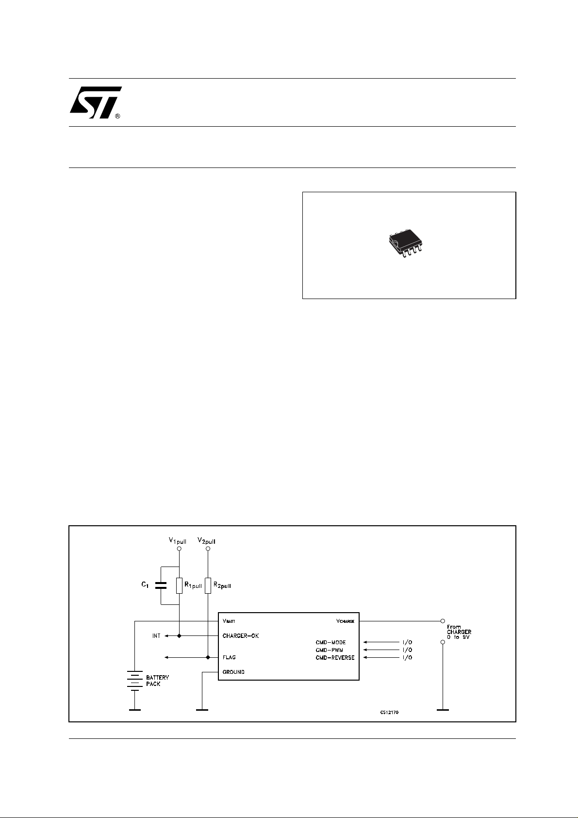
This specification describes a dedicated I.C.
which allows to charge 1 Lilon cell or 3 Nimh cells.
The principle used to charge the batteries is the
pulsed current, the monitoring is operated by the
micro-contoller of the application. This I C
integrates one Power Switch and achieves the
ST3S01LED
BATTERY CHARGE I.C.
SO-8
exposed pad
charge bat teries in two different modes charg e or
precharge.
One of this operating m ode (charge or precharge)
can be sel ec ted in a static or pulsed way by one I/
O from a micro-controller. The I C can supply
power to accessories controlled by this I.C. in
Reverse mode. The I.C. is available in the smaller
and surface mounted S O-8 (exposed pad version)
package.
SCHEMATIC DIAGRAM
1/17March 2003
Page 2
ST3S01LED
ABSOLUTE MAXIMUM RATINGS
Symbol Parameter Value Unit
V
BATT
V
CHARGE
V
FLAG
V
CHARGER-OK
V
CMD-PWM
V
CMD-MODE
V
CMD-REVERSE
I
SWITCH
T
stg
T
J
T
AMB
Absolute Maximum Ratings are those values beyond which damage to the device may occur. Functional operation under these condition is
not implied.
(*) The I.C. is automatically turned OFF when V
falling edge)
Battery Voltage
Charge Voltage (*)
(V
CHARGE-VBATT
) Flag Control Voltage
Charger Flag Control Voltage
PWM Command Voltage
CMD Command Voltage
Reverse Command Voltage
Internal Switch
Continuous Max Current
Internal Switch Peak
Current
T
= 85°C, R
AMB
= 30°C, R
T
AMB
thj-amb
thj-amb
= 40°C/W
= 40°C/W
T<1ms Duty Cycle < 1%
thj-amb
= 40°C/W
R
Storage Temperature Range
Operating Junction Temperature Range
Operating Ambient Temperature Range (if an adeguate
heatsink is provided)
reaches typically 14V (V
CHARGE
CHARGE
-0.3 to 6 V
-12 to 16 V
-0.3 to 12 V
-0.3 to 12 V
-0.3 to 5 V
-0.3 to 5 V
-0.3 to 5 V
2A
3A
8A
-55 to +125 °C
-40 to +125 °C
-40 to +85 °C
rising edge); typical hysteresis is 700mV (V
CHARGE
THERMAL DATA
Symbol Parameter SO-8 Unit
R
thj-case
Thermal Resistance Junction-case
10 °C/W
ORDERING CODES
TYPE SO-8 exposed pad SO-8 exposed pad (T&R)
ST3S01LED ST3S01LED ST3S01LED-TR
CONNECTION DIAGRAM (top view)
2/17
Page 3
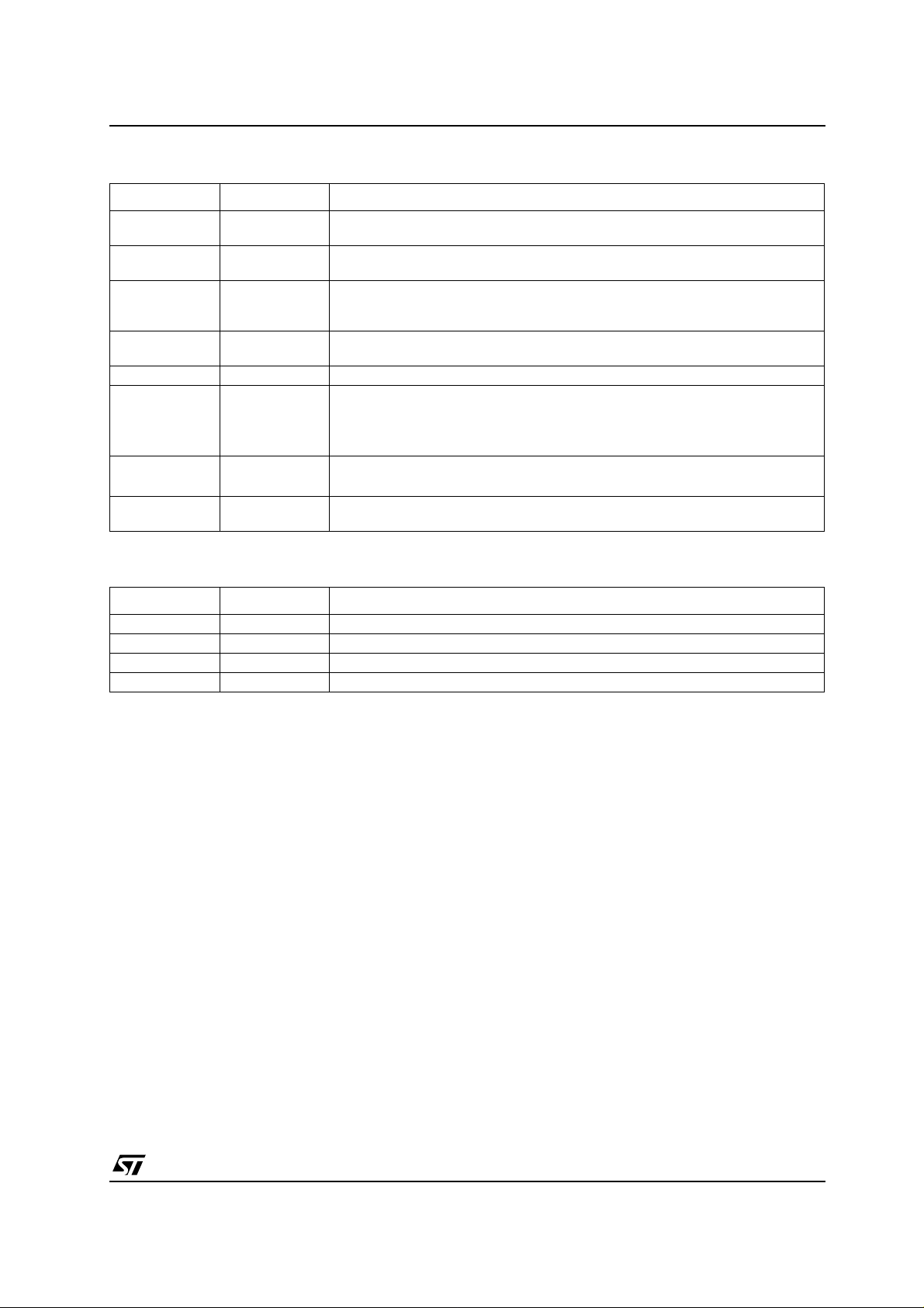
PIN DESCRIPTION
Pin N° Symbol Name and Function
1V
BATT
2 CMD-REVERSE Reverse Command pin: Enables the reverse mode when connected to a positive
3 CMD-PWM PWM Command pin: allows to control the precharge or charge switch in PWM
4 CMD-MODE Mode Command pin: allows to switch between precharge and charge mode (refer
5 GND GND Pin
6 CHARGER-OK CHARGER-OK output pin; open drain N-channel MOSFET that is in high
7 FLAG FLAG pin (V
8V
CHARGE
BATTERY pin: input pin when reverse mode is selected; output pin when in
charge or precharge mode
voltage higher than 1.2V. Logic pin internally pulled down.
mode (refer to the Table 1 for the different operating modes). Logic pin internally
pulled down.
to OPERATING MODES Table). Logic pin internally pulled down.
impedance when the V
CHARGE
voltage drops below 2.5V and CMD-REVERSE is
low. When the reverse function is activated, this open drain have the same
information of the (V
when the V
CHARGE-VBATT
CHARGE
CHARGE-VBATT
): open drain N-channel MOSFET that sinks current
voltage is higher than the V
) FLAG.
CHARGER SUPPLY pin: input pin when charge or precharge mode is selected;
output pin when in reverse mode.
BATT
ST3S01LED
.
OPERATING MODE
CMD-PWM CMD-MODE Operating Function Selected
0 0 PRECHARGE MODE (Default state)
0 1 CHARGE MODE
1 0 CHARGE and PRECHARGE switches are open
1 1 CHARGE and PRECHARGE switches are open
3/17
Page 4
ST3S01LED
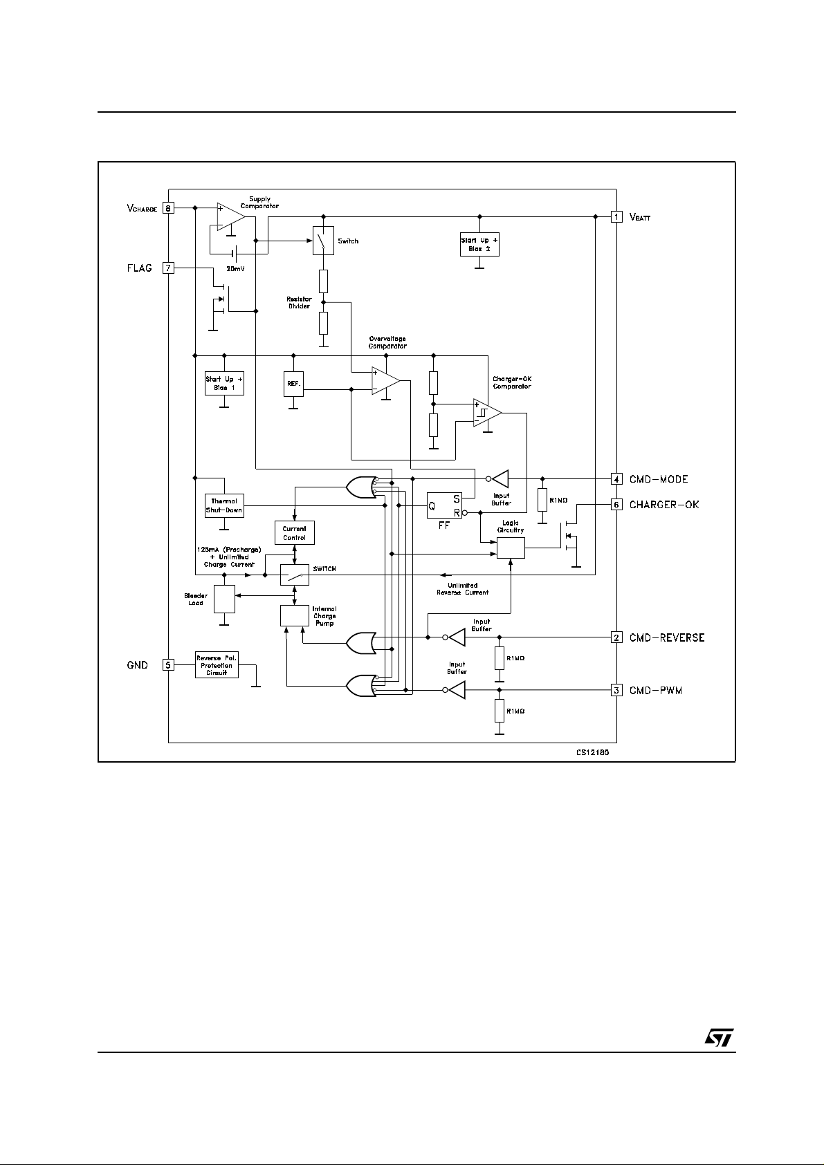
I.C. BLOCK DIAGRAM
POSSIBLE OPERATING MODES
Five different operating m odes are allowed:
charge, precharge, reverse, charge+reverse and
precharge+reverse. These op erating modes can
be achieved by properly selection of the
CMD-REVERSE C MD-PWM and CMD-MODE
(See POSSIBLE OPERATING MODE Table).
PRECHARGE MODE
The PRE CHARGE function is compos ed by a
switch and a 100mA current source which fully
works for V
CHARGE
higher than 2.5V. When the
CMD-MODE and the CMD-PWM are not leaded
the switc h is ON, being the i nput states held by an
internal pull down resistor. This is used when the
4/17
battery is strongly discharged. In this case V
BATT
can be null (battery empty) and all the i nput pins
are not held by any level (because the
micro-controller is down), except the V
CHARGE
pin
which is a main supply. The source of current
supplies a const ant current into the battery till its
voltage level reaches the required level allowing to
start the micro-controller (typically 3V ). The
current direction is from V
CHARGE
to V
BATT
.The
reverse leakage current when the swich is ON
must be null; this is obtained thanks t o an internal
circuitry that switch OFF the internal P-MOS when
the V
is higher than V
BATT
CHARGE
,whateverthe
status of the CMD -MO D E. The precharge function
is also used to adjust the mean current. When the
Page 5

ST3S01LED
battery is fully charged the current into the battery
has not to be more than C/25 (Nimh battery). In
order to perform finely this, the CMD-PWM pin
must be d riven with PWM funct ion (in the same
time, the CMD-MODE must be kept low). T he duty
cycle allows to adjust the mean current needed.
CHARGE MODE
TheCMD-MODEpin,whenhigh(andCMD-PWM
low), handles t he switch in charge mode. This
switch allows the battery charge with a strong
current. The drop of this internal P -Channel MOS
is very low (200mV @ 800mA ) in order to optimize
the efficiency of the charge.
The switch is not internally protected against short
circuit or overcurrent condition.
When the s witch is ON (CMD-MODE high and
CMD-PWM low), the current direction into the chip
is from V
CHARGE
to V
. The reverse current
BATT
when the switch is ON m us t be null; t his is
obtained by mean of an internal circu itry that
switch OFF the internal P - MOS when the V
higher than V
CHARGE
, whatever the status of the
BATT
is
CMD-MODE. When the CMD-MODE pin is lo w or
in high impedance t he switch is OFF, while it is ON
when the signal on that pi n is high.
REVERSE MODE
When the reverse function i s selected by
CDM-REVERSE pin, the switch allows to supply
the accessories with a strong current. The drop of
the internal P-Channel MOS is very low (200mV
@ 800mA)and theswitchproperlywork for V
BATT
higher than 2.5V. This allows to supply energy on
the V
CHARGE
pin. When the switch is ON
(CMD-REVERSE high ) the current direction into
thechipisfromV
The reverse current (from V
BATT
to V
CHARGE
CHARGE
.
to V
BATT
when the switch is ON m us t be null; t his is
obtained by mean of an internal circu itry that
switch OFF the internal P-MOS when the
V
CHARGE
is higher than V
, whatever the
BATT
status of the CMD-REVERSE. When the level of
CMD-REVERSE pin is low or in high impedance,
the switch is OFF, while it is ON when the signal
on CMD-REVERSE pin is high.
OVERVOLTAGE PROTECTION
This function allows to held the switches OFF
when the voltage level on V
is higher than a
BATT
maximum voltage whatever are the values of
CMD-PWM, CMD-MODE and CMD-REVERSE.
This maximum volt age is shown in the electrical
characteristic (typical threshold 5.7V). From the
moment in which the o.v.protection is activated, it
will be possible to turm ON again the switch only
when th e V
CHARGE
value decreases down to 2.5V
typically, it doesn't matter which operation mode is
selected. The protection works only when the
battery is in charge or precharge mode, i.e.
V
CHARGE>VBATT
.
This represent s, in fact, the typical application
condition where the battery could increase its
value, i.e. When charge or precharge mode are
used.
CHARGER DETECTION MODE
This function allows to generate a digital signal
(CHARGER-OK) to indicate if the V
voltage is higher than 2.5V and the revers e
function is inactive. This functionality allows to
determine if the charger is present or not; if t he
V
CHARGE
is lower than the 2.5V, the
CHARGER-OK goes into high impedance (open
drain). When the reverse function is act ive, this
open drain have the V
CHARGE-VBATT
This circuitry is d irectly supplied from V
and works only for V
V
CHARGE-VBATT
DETECTION MODE
CHARGE
higher than 2.2V.
This function allows to generate a digital signal
(V
CHARGE-VBATT
voltage is higher than V
lower than the V
)flagtoindicateiftheV
;iftheV
BATT
, this open drain goes into
BATT
high impedance s tate. This circuitry is directly
supplied from V
V
CHARGE
higher than 2.2V.
CHARGE
pin an d works only for
THERMAL PROTECTION
An internal thermal shutdown circuitry will switch
OFF the P_MOS, only in precharge or in charge
mode, when the junction temperature reaches
typically 180°C. This has been impl emented in
)
order to protect the device from overburning. 20°C
of thermal hysteresis will avoid a thermal
oscillation.
This circuitry is supplied from V
CHARGE
acts only on t he prec harge and c harge s witche s.
ESD PROTECTION
Both V
CHARGE
and V
pins are protected
BATT
against electrostatic discharge up to ±4KV (HBM,
MIL STD 833D.
CHARGE VOLTAGE
V
CHARGE
to12V.AtV
functional operating range is from 2.5V
CHARGE
=14V typically the I.C. is
automatically turned OFF and remains OFF up to
16V. A V
CHARGE
voltage higher than 16V can
damage the IC.
CHARGE
information.
CHARGE
CHARGE
pin
CHARGE
and, so,
is
5/17
Page 6
ST3S01LED
POSSIBLE OPERATING MODE
CMD-PWM CMD-MODE CMD-REVERSE Operating Function Selected
0 0 0 PRECHARGE
0 0 1 PRECHARGE + REVERSE
0 1 0 CHARGE
0 1 1 CHARGE + REVERSE
1 0 0 SWITCH OPEN
1 0 1 REVERSE
1 1 0 SWITCH OPEN
1 1 1 REVERSE
ELECTRICAL CHARACTERISTICS OF REVERSE SWITCH (T
= - 40 to 85°C, unless otherwise
A
specified.)
Symbol Parameter Test Conditions Min. Typ. Max. Unit
V
BATT
V
DROP
I
LEAKAGE
V
IH
V
IL
V
TH
I
CMD-REV
t
ON-OFF
Reverse Block Operating
2.5 6 V
Input Voltage
Dropout Voltage V
Reverse Leakage Current
(from V
CHARGE
tested on V
to V
BATT
pin)
BATT
,
CMD-REVERSE Logic
High (Switch ON)
CMD-REVERSE Logic
Low (Switch OFF)
CMD-REVERSE Logic
Typical Threshold
CMD-REV Input Current V
=3V I
BATT
V
CMD-REVERSE
V
CMD-MODE
V
=0V V
BATT
V
CMD-REVERSE
V
CMD-MODE
V
=3V I
BATT
V
CMD-PWM
V
=3V I
BATT
V
CMD-PWM
V
=3V I
BATT
V
CMD-PWM
=3V I
BATT
V
CMD-REVERSE
V
CMD-MODE
=5V I
V
BATT
V
CMD-REVERSE
V
CMD-MODE
=1.9V, V
=1.9V
=1.9V, V
=1.9V
=1.9V V
=1.9V V
=1.9V V
=1.9V, V
=1.9V
=1.9V, V
=1.9V
REVERSE
CMD-PWM
CHARGE
CMD-PWM
REVERSE
CMD-MODE
REVERSE
CMD-MODE
REVERSE
CMD-MODE
REVERSE
CMD-PWM
REVERSE
CMD-PWM
=800mA
=1.9V
=9V
=1.9V
=10mA
=1.9V
=10mA
=1.9V
=10mA
=1.9V
=10mA
=1.9V
=10mA
=1.9V
130 200 mV
01µA
1.2 V
0.4 V
0.75 V
1 1.9 3 µA
10 µA
Response Time 100 µs
6/17
Page 7

ST3S01LED
ELECTRICAL CHARACTERISTICS OF PRECHARGE SWITCH (TA= -40 to 85°C, unless o therwise
specified.)
Symbol Parameter Test Conditions Min. Typ. Max. Unit
V
CHARGE
V
DROP
I
PRECHARGE
I
LEAKAGE
F
MODE
t
ON-OFF
t
OFF-ON
Precharge Block
2.5 12 V
Operating Input Voltage
Dropout Voltage V
Precharge Current Limit
(from V
CHARGE
to V
BATT
)
Precharge Leakage
Current Limit (from V
to V
V
CHARGE
CHARGE
, tested on
pin)
BATT
PRECHARGE Switch
Minimum Frequency
= 2.5V to 9V
CHARGE
I
PRECHARGE
V
CMD-REVERSE
V
CMD-PWM
V
CMD-MODE
V
V
V
V
V
V
V
V
V
V
V
V
V
V
V
V
V
= 2.5V to 5VV
CHARGE
CMD-REVERSE
CMD-PWM
CMD-MODE
= 2.5V to 9VV
CHARGE
CMD-REVERSE
CMD-PWM
CMD-MODE
=0V V
CHARGE
CMD-REVERSE
CMD-PWM
CMD-MODE
= 2.5V to 9V
CHARGE
=0VtoV
BATT
CMD-REVERSE
CMD-PWM
CMD-MODE
=100mA
=0V or floating
=0V or floating
=0V or floating
BATT
=0V or floating
=0V or floating
=0V or floating
BATT
=0V or floating
=0V or floating
=0V or floating
BATT
=0V or floating
=0V or floating
=0V or floating
CHARGE
=0V or floating
=0V or floating
=0V to 1.9V at F
=0V
=0V
= 5.5V
MODE
100 170 mA
100 200
100 Hz
0.13 1.2 V
1 µA
Response Time 100 µs
Response Time 100 µs
7/17
Page 8

ST3S01LED
ELECTRICAL CHARACTERISTICS OF CHARGE SWITCH (TA= -40 to 85°C, unless otherwise
specified.)
Symbol Parameter Test Conditions Min. Typ. Max. Unit
V
CHARGE
V
DROP
I
LEAKAGE
V
IH
V
IL
V
TH
I
CMD-REV
F
MODE
t
ON-OFF
Charge Block Operating
2.5 12 V
Input Voltage
Dropout Voltage V
Precharge Leakage
Current Limit (from V
to V
V
CHARGE
CHARGE
, tested on
pin)
BATT
CMD-MODE Logic High
(CHARGE MODE ON)
CMD-MODE Logic Low
(CHARGE MODE OFF)
CMD-MODE Logic
Typical Threshold
CMD-MODE Input
Current
PRECHARGE Switch
Minimum Frequency
I
CHARGE
V
V
V
V
V
I
CHARGE
V
V
I
CHARGE
V
V
I
CHARGE
V
V
V
V
V
I
CHARGE
V
V
= 2.5V to 5V
CHARGE
=800mA V
CMD-PWM
CHARGE
CMD-REVERSE
CMD-MODE
CHARGE
=0V V
=0V V
=1.9V
= 2.5V to 5V
=10mA V
CMD-PWM
CHARGE
=0V
= 2.5V to 5V
=10mA V
CMD-PWM
CHARGE
=0V
= 2.5V to 5V
=10mA V
CMD-PWM
CHARGE
CMD-REVERSE
CMD-MODE
CHARGE
=0V
=3Vto5V I
=1.9V
= 2.5V to 5V
=10mA V
CMD-PWM
CMD-MODE
=0V
=0V to 1.9V at F
CMD-REVERSE
=0V V
CMD-REVERSE
CMD-REVERSE
CMD-REVERSE
=0V V
CMD-REVERSE
CMD-MODE
= 5.5V
BATT
CMD-PWM
CHARGE
CMD-PWM
MODE
=0V
=1.9V
=0V
=0V
=0V
=0V
=10mA
=0V
=0V
0.13 0.2 V
1 µA
1.2 V
0.4 V
0.75 V
130µA
100 Hz
Response Time 100 µs
ELECTRICAL CHARACTERISTICS OF CMD-PWM LOGIC PIN (T
=-40to85°C,V
A
CHARGE
= 2.5 to 9V
unless otherwise specified.)
Symbol Parameter Test Conditions Min. Typ. Max. Unit
I
CMD-PWM
8/17
V
IH
V
IL
V
TH
CMD-PWM Logic High
(SWITCH OFF)
CMD-PWM Logic High
(SWITCH ON)
CMD-PWM Logic Typical
Threshold
CMD-PWM Input Current I
I
PRECHARGE
V
CMD-REVERSE
I
PRECHARGE
V
CMD-REVERSE
I
PRECHARGE
V
CMD-REVERSE
PRECHARGE
V
CMD-REVERSE
V
CMD-MODE
=10mA
=0V V
=10mA
=0V V
=10mA
=0V V
=10mA
=0V V
=1.9V
CMD-MODE
CMD-MODE
CMD-MODE
CMD-MODE
1.2 V
=0V
0.4 V
=0V
0.75 V
=0V
130µA
=0V
Page 9

ST3S01LED
ELECTRICAL CHARACTERISTICS OF CHARGER DETECTION BLOCK (TA= -40 to 85°C,
V
CHARGE
V
V
CHARGE-TH
V
CHARGE-HYS
V
CHARGER-OK
V
CHARGER-OK
I
CHARGER-OK
I
CHARGER-OK
=2.2to9V,V
CMD-REVERSE
= 0V or floating un less otherwise specified.)
Symbol Parameter Test Conditions Min. Typ. Max. Unit
CHARGE
Charger Detection Block
Operating Input Voltage
2.2 V
Low Voltage Threshold with falling edge 2.425 2.5 2.575 V
Low Voltage Hysteresis with rising edge, TA=25°C 100 mV
CHARGER-OK Output
Voltage Low
CHARGER-OK Output
Voltage Low
CHARGER-OK Output
Leakage Current
CHARGER-OK Output
Leakage Current
V
CHARGE
V
FLAG
V
CMD-REVERSE
V
CHARGE
V
FLAG
V
CMD-REVERSE
=3V I
= 0.2V I
= 2.2V V
= 0.2V V
CHARGER-OK
CHARGER-OK
=1.9V
=1.9V
CHARGER-OK
CHARGER-OK
=1mA 0.2 0.4 V
=1mA
0.2 0.4 V
=10V 0 1 µA
=10V
01µA
ELECTRICAL CHARACTERISTICS OF FLAG DETECTION BLOCK (T
=-40 to 85°C, V
A
CHARGE
to 9V unless ot herwise s pec ified.)
Symbol Parameter Test Conditions Min. Typ. Max. Unit
V
CHARGE
V
VCHARGE-
VBATT
I
VCHARGE-
VBATT
V
VCHARGE-
VBATT
I
VCHARGE-
VBATT
FLAG Detection Block
Operating Input Voltage
FLAG (V
CHARGE-VBATT
Voltage Low
FLAG (V
CHARGE-VBATT
Leakage Current
FLAG* (V
CHARGE-VBATT
Voltage Low
FLAG* (V
CHARGE-VBATT
Leakage Current
)
V
= 0.2V I
FLAG
)
V
= 0.2V I
FLAG
)
I
CHARGE
)
V
BATT=VCHARGE
=20mA I
=1mA 0.2 0.45 V
FLAG
=10mA 1 µA
FLAG
=1mA 0.2 0.45 V
FLAG
V
= 10V 1 µA
FLAG
2.2 V
* Guaranteed by design
ELECTRICAL CHARACTERISTICS OF OVERLOAD PROTECTION (T
V
CHARGE>VBATT,VCMD-REVERSE
=0V, V
CMD-PWM
=0V, V
CMD-MODE
=0V to 1.9V, unless otherwise
=-40 to 85°C, V
A
CHARGE
specified.)
Symbol Parameter Test Conditions Min. Typ. Max. Unit
V
BATT
t
ON-OFF
Battery Input Threshold with rising edge 5.4 5.6 5.9 V
Response Time Switches ON to OFF, TA= 25°C 100 µs
=2.2
>3V,
9/17
Page 10

ST3S01LED
I.C. CONSU MPTION (TA=-40 to 85°C, V
CHARGE<VBATT
, unl es s otherwise specified. )
Symbol Parameter Test Conditions Min. Typ. Max. Unit
I
BATT
I
CHARGE
Current Consumption
from Battery Pin
Current Consumption
from the Charge Pin
V
CMD-PWM
V
CMD-MODE
= 3 to 5.25V
V
BATT
V
CHARGE
V
CMD-REVERSE
V
BATT
V
CHARGE
V
CMD-REVERSE
V
CHARGE
V
CMD-REVERSE
V
CMD-MODE
= floating
= 5.25V
= floating
= 5.25V V
=1.9V
=0V or 1.9V
=0V
=1.9V
=0V V
=0V or 1.9V
= floating
BATT
CMD-PWM
15 µA
140 300 µA
78 250 µA
=1.9V
ESD PROTECTION
Symbol Parameter Test Conditions Min. Typ. Max. Unit
T
ESD Electrostatic Discharge
Immunity for V
and V
BATT
CHARGE
pins
=25°C
A
Human Body Method MIL STD
833D-3015.7
TYPICAL P E RFORMAN CE CHARACTERISTICS (unless otherwise specified T
Figure1 : Pr ec harge Current Limit vs
Figure2 : Charge Drop Voltage vs Temperature
±4 kV
=25°C)
j
Temperature
µA
10/17
Page 11

ST3S01LED
Figure3 : Current Cons umption vs Temperature
Figure4 : Pr ec harge Drop V oltage v s
Temperature
Figure6 : V
Leakage Current vs
BATT
Temperature
Figure7 : Reverse C urrent Consumption v s
Temperature
Figure5: Reverse Drop Voltage vs Temperature
Figure8 : CMD-Mode Logic Threshold vs
Temperature
11/17
Page 12

ST3S01LED
Figure9 : Command PWM Logic Threshold vs
Temperature
Figure10 : CMD-MODE Input Current vs
Temperature
Figure12 : CMD-REVERSE Input Current vs
Temperature
Figure13 : CMD-PWM Input Current vs
Temperature
Figure11 : Command Reverse Logi c vs
Temperature
12/17
Figure14 : CHARGER OK Voltage vs
Temperature
Page 13

ST3S01LED
Figure15 : CHARGER OK Voltage vs
Temperature
Figure16 : CHARGER OK Voltage Thresold vs
Temperature
Figure18 : Minimum Battery Current vs
Temperature
Figure19 : Minimum Battery Current vs
Temperature
Figure17 : Flag Voltage Low vs Temperature
Figure20 : Overvoltage Protection v s
Temperature
13/17
Page 14

ST3S01LED
Figure21 : Dynamic Precharge Mode
14/17
Page 15

SO-8 (exposed pad) MECHANICAL DATA
ST3S01LED
DIM.
A 1.25 1.62 0.049 0.064
a1 0 0.10 0.000 0.004
a2 1.10 1.65 0.043 0.064
a3 0.65 0.85 0.025 0.033
b 0.33 0.51 0.013 0.020
b1 0.19 0.25 0.007 0.010
C 0.25 0.50 0.010 0.019
c1 45˚ (max.)
D 4.80 5.00 0.189 0.196
E 5.80 6.20 0.228 0.244
e 1.27 0.050
e3 3.81 0.150
F 3.80 4.00 0.149 0.157
L 0.40 1.27 0.016 0. 050
M 0.6 0.023
S ˚ (max.)
MIN. TYP MAX. MIN. TYP. MAX.
mm. inch
8
A
A
0,10
B
B
15/17
Page 16

ST3S01LED
Tape & Reel SO-8 MECHANICAL DATA
mm. inch
DIM.
MIN. TYP MAX. MIN. TYP. MAX.
A 330 12.992
C 12.8 13.2 0.504 0.519
D 20.2 0.795
N 60 2.362
T 22.4 0.882
Ao 8.1 8.5 0.319 0.335
Bo 5.5 5.9 0.216 0.232
Ko 2.1 2.3 0.082 0.090
Po 3.9 4.1 0.153 0.161
P 7.9 8.1 0.311 0.319
16/17
Page 17

ST3S01LED
Information furnished is believed to be accurate and reliable. However, STMicroelectronics assumes no responsibility for the
consequences of use o f suc h inf ormat ion n or f or an y infr ingeme nt of paten ts or oth er ri gh ts of third part ies whic h may resul t f rom
its use. No license is granted by implication or otherwise under any patent or patent rights of STMicroelectronics. Specifications
mentioned in this publication are subject to change without notice. This publication supersedes and replaces all information
previously supplied. STMicroelectronics products are not authorized for use as critical components in life support devices or
systems without express written approval of STMicroelectronics.
Australia - Brazil - Canada - China - Finland - France - Germany - Hong Kong - India - Israel - Italy - Japan - Malaysia - Malta - Morocco
© The ST logo is a registered trademark of STMicroelectronics
© 2003 STMicroelectronics - Printed in Italy - All Rights Reserved
STMicroelectronics GROUP OF COMPANIES
Singapore - Spain - Sweden - Switzerland - United Kingdom - United States.
© http://www.st.com
17/17
 Loading...