

Page 1
ST3M01
TRIPLE VOLTAGE REGULATOR
■ ONLY TWO CELL NEED AS INPUT
■ THREE REGULATED OUTPUT
1) HIGH EFFICENCY PFM DC/DC
CONVERTER 3.3V AT 200mA (87%
EFFICENCY)
2) VERY LOW NOISE AND VERY LOW
DROP V
(3V AT 20mA)
REG
3) VERY LOW NOISE AAND VERY LOW
DROP V
■ LOGIC CONTROLLED ELECTRONIC
(1.9 V AT 20m A)
REG
SHUTDOWN
■ LOW BATTERY DETECTOR
■ VIRTUAL GND PIN
■ TEMPERATURA RANGE: -40 TO 85°C
SO-14
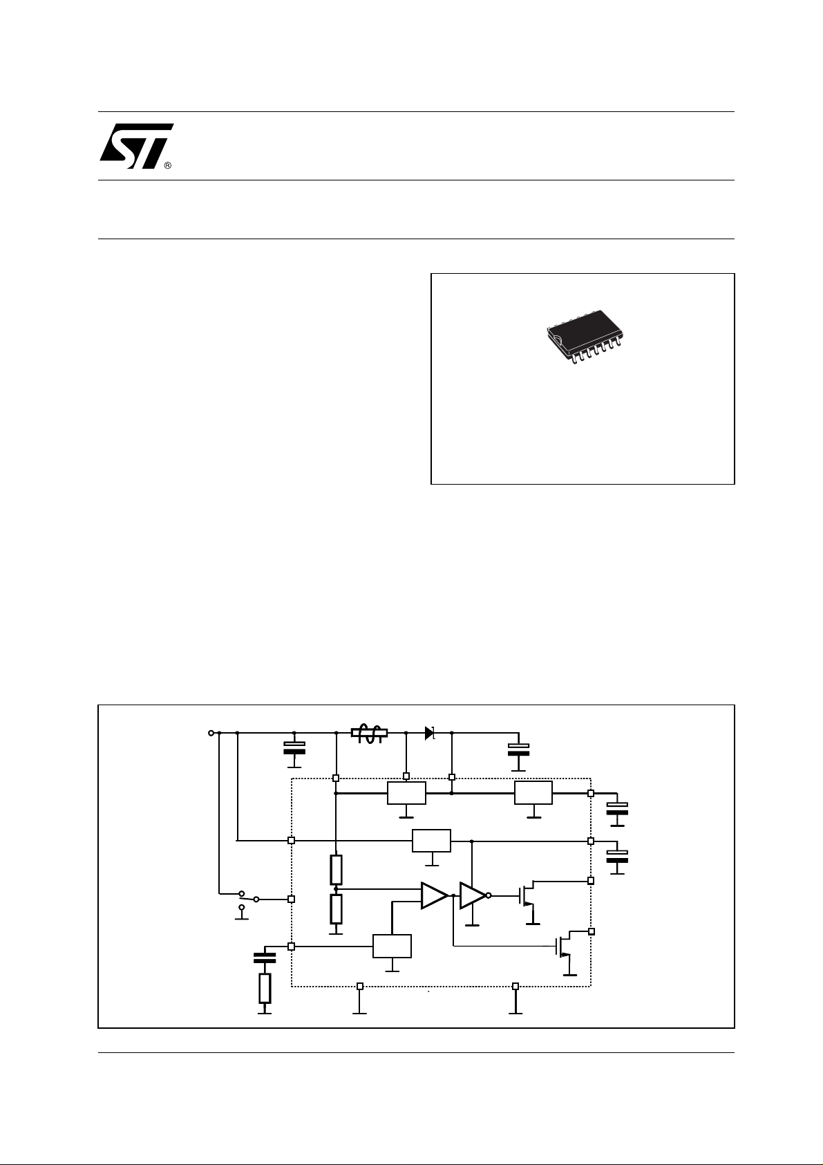
SCHEMATIC DIAGRAM
Vin
On-Mode
Off-Mode
100 nF
1 KΩ
150 µF
IN_Linear
SHDN
Vref
IN_SW
15 µH
GND_SW
DC/DC
DC/DC
Ref
Ref
Lx
Linear B
-
+
OUT DC/DC
150 µF
Linear A
GND_Signal
OUT LA
1 µF
OUT LB
1 µF
Virtual GND
LBO
1/11November 2000
Page 2

ST3M01
ABSOLUTE MAXIMUM RATINGS
Symbol Parameter Value Unit
V
V
SHDN
V
V
LBO
V
virtua l_ GND
I
LBO
I
virtual_GND
T
T
THERMAL DATA
Symbol Parameter Value Unit
R
thj-amb
ORDER CODES
LX
stg
op
DC Input Voltage (Both IN_Linear and IN_SW)
IN
Shutdown Input Voltage -0.3 to VIN+0.3
Switch Voltage
Low Battery Output Voltage
Virtual GND Output Voltage
Low Battery Output Maximum Current
Virtual GND Output Maximum Current
Storage Temperature Range
Operating Junction Temperature Range
Thermal Resistance Junction-ambient (*)
-0.3 to 7 V
-0.3 to 7 V
-0.3 to 7 V
-0.3 to 7 V
30 mA
30 mA
-65 to +150 °C
-40 to +85 °C
160 °C/W
V
Type Package Comment
ST3M01D SO-14 50 parts per tube / 20 tube per box
ST3M01DTR SO-14 (Tape & Reel) 2500 parts per reel
2/11
Page 3
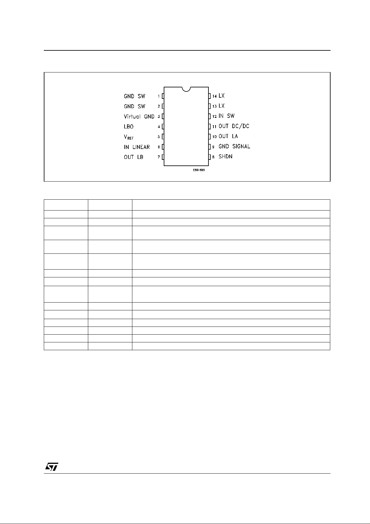
CONNECTION DIAGRAM (top view)
PIN DESCRIPTION
Pin N° Symbol Name and Function
1 GND SW Switching Ground. Must be low impedance; solder directly to GND plane
2 GND SW Switching Ground. Must be low impedance; solder directly to GND plane
3 Virtual GND Virtual GND. Open Drain N-Cnannel MOSFET: must be high impedance when the
Low Battery condition is detected.
4 LBO Low Battery Output. Open Drain N-Cnannel MOSFET: sinks current when the
input voltage drops below 2V typically.
5V
REF
Reference Voltage Output. Bypass with 0.1 µF to improve the linears V
thermal noise performance
.
6 IN Linear Linear Input. Must be connected togheter with IN SW to the input supply.
7OUT L
8 SHDN
Linear B Output port. 1.9V typically.
B
Shutdown Input. Disables the SMPS and L
referencevoltage and the low batery comparator remain active.
9 GND Signal Signal GND. Must be connected togheter with the Switching Ground.
10 OUT L
11 OUT DC/DC DC/DC Output Port: 3.3V typically.
12 IN SW SMPS Input. Must be connected togheter with IN_Linear to the input supply.
13 LX 1.5A N-Channel Power MOSFET Drain.
14 LX 1.5A N-Channel Power MOSFET Drain.
Linear A Output port. 3V typically.
A
output, but the L
A
ST3M01
REF
, the
B
3/11
Page 4
ST3M01
ELECTRICAL CHARACTERISTICS (Unless otherwise specified, please refer to the typical operating
circut of the pag 1 for the external components values and connections. Unless otherwise noted
=HIGH)
V
SHDN
Symbol Parameter Test Conditions Min. Typ. Max. Unit
V
V
O(DC/DC)
ν DC/DC Converter Efficency V
V
O(LA)
V
O(LB)
e
N(LA)
e
N(LB)
I
q(OFF)
I
q(OFF)
I
S(DC/DC)
I
q(LA)
I
q(LB)
V
BATT
V
BATT(HYS)
R
ON(LBO)
V
V
T
on
R
ON(V_GND)
Note 1: For VIN < 1.9V the V
Note 2: V
Operating Input Voltage 1.9 3.3 V
I
DC/DC Converter Output
Voltage (Test Circuit A)
Linear A Output Voltage
(Test Circuit A)
Linear B Output Voltage
(Test Circuit A)
Linear A Thermal Output
Noise Voltage (Note 2)
Linear B Thermal Output
Noise Voltage (Note 2)
Quiescent Current OFF
Mode DC/DC & L
OFF LB
A
ON) (Test Circuit E)
Quiescent Current OFF
Mode (DC/DC & L
OFF LB
A
ON) (Test Circuit F)
DC/DC Supply Current
2.24<VIN<3.3V; 0<I
0<I
-40 < T
I
<20mA; 0<I
O(LA)
< 85 °C
J
=2.4V; I
IN
=0mA; I
O(LA)
O(DC/DC)
=0mA; TJ = 25°C
O(LB)
2.24<VIN<3.3V; 0<I
0<I
-40 < T
<20mA; 0<I
O(LA)
< 85°C
J
2.24<VIN<3.3V; 0<I
0<I
-40 < T
VIN=2.4V; V
I
C
VIN=2.4V; V
I
C
V
T
V
T
<20mA; 0<I
O(LA)
< 85°C
J
=20mA; 10 < f < 80KHz;
O(LA)
=1µF; C
O(LA)
=20mA; 10 < f < 80KHz;
O(LB)
=1µF; C
O(LB)
=3.3V; No Load; V
IN
= 25°C
J
=1.9V; No Load; V
IN
= 25°C
J
O(DC/DC)
=0.1µF; TJ = 25°C
REF
O(DC/DC)
=0.1µF; TJ = 25°C
REF
O(DC/DC)
O(LB)
O(DC/DC)
O(LB)
O(DC/DC)
O(LB)
<200mA;
<20mA;
=100mA;
<200mA;
<20mA;
<200mA;
<20mA;
=3.5V;
=3.5V;
=LOW;
SHDN
=HIGH;
SHDN
VIN=2.24V; No Load; TJ = 25°C 100 µA
3.2 3.3 3.415 V
87 %
2.93 3 3.09 V
1.86 1.9 1.955 V
60 µV
35 µV
75 µA
50 µA
(Test Circuit B)
Linear A Quiescent Current
(Test Circuit C)
Linear B Quiescent Current
(Test Circuit C)
Low Battery Detection
Range
Low Battery Detection
VIN=2.24V; V
I
=10mA; TJ = 25°C
O(LA)
VIN=2.24V; V
I
=10mA; TJ = 25°C
O(LB)
V
=HIGH with falling edge 1.96 2 2.04 V
SHDN
O(DC/DC)
O(DC/DC)
=3.5V;
=3.5V;
220 µA
75 µA
150 200 mV
Hysteresys
LBO R
DSON
Control Input Logic Low VIN>2.24V; -40 < TJ < 85°C 0.4 V
ih
Control Input Logic High VIN>2.24V; -40 < TJ < 85°C 1.5 V
il
Timer On Response Time
on DC/DC
VIN=1.9V; ID=5mA; TJ = 25°C 10 Ω
VIN=2.4V; CO=100µF; TJ = 25°C
I
O(DC/DC)
V
=200mA
=from GND to V
SHDN
SHDN(MAX)
0.6 9 ms
Virtual GND RDSON VIN>2.24V; ID=5mA; TJ = 25°C 10 Ω
is out of regul ation because of under dropout con di tion
= 3.5V force for an extern al DC source t o avoid switching noise
O(DC/DC)
O(LB)
rms
rms
4/11
Page 5

DC/DC CONVERTER BLOCK DIAGRAM
ST3M01
LINEAR VREG BLOCK DIAGRAM
5/11
Page 6

ST3M01
TEST CIRCUIT A
Vin
150 µF
IN_Linear
On-Mode
Off-Mode
0.1 µF
SHDN
1 KΩ
TEST CIRCUIT B
Vref
15 µH
IN_SW
DC/DC
Ref
Ref
GND_SW
DC/D C
Lx
Linear B
-
+
OUT DC/DC
150 µF
Linear A
GND_Signal
V
OUT LA
V
OUT LB
V
Virtual GN D
LBO
1 µF
1 µF
Vin
47 µF
0.1 µF
(Isup)DC/DC
A
IN_Linear
SHDN=HIGH
Vref
1 KΩ
47 µF
15 µH
IN_SW
DC/DC
Ref
Ref
GND_SW
DC/DC
Lx
Linear B
-
+
OUT DC/DC
150 µF
Linear A
GND_Signal
OUT LA
1 µF
OUT LB
1 µF
Virtual GND
LBO
6/11
Page 7

TEST CIRCUIT C (Iq)Ia=(Iin)Ia-(Iout)Ia
ST3M01
(Vin)DC/DC F loating
(Vin)Lin=2.24V
IN_Linear
47 µF
SHDN=HIGH
Vref
0.1 µF
1 KΩ
47 µF
15 µH
IN_SW
DC/DC
Ref
Ref
GND_SW
DC/DC
Lx
Linear B
-
+
(Iin)la
A
OUT DC/DC
(Vout)DC/DC =3.5V
Linear A
GND_Signal
OUT LA
OU T LB
Virtual GND
LBO
(Iout)la
1 µF
1 µF
TEST CIRCUIT D (Iq)Ib=(Iin)Ib-(Iout)Ib
(Vin)DC/DC F l o ating
47 µF
(Vin)Lin=3.3V
(Iin)lb
15 µH
IN_SW
A
IN_Linear
47 µF
SHDN=LOW
Vref
0.1 µF
1 KΩ
GND_SW
DC/DC
DC/DC
Ref
Ref
Lx
Linear B
-
+
OUT DC/DC
150 µF
Linear A
GND_Signal
OUT LA
OUT LB
Virtual GND
LBO
1 µF
(Iout)lb
1 µF
7/11
Page 8

ST3M01
TEST CIRCUIT E
Vin = 3.3V
A
Iq = off
150 µF
15 µH
IN_SW
DC/DC
DC/DC
Lx
OUT DC/DC
150 µF
Linear A
OUT LA
1 µF
IN_Linear
SHDN= LOW
0.1 µF
1 KΩ
TEST CIRCUIT F
Vin = 1.9V
A
Iq = off
Vref
150 µF
15 µH
IN_SW
Ref
Ref
GND_ SW
DC/DC
DC/DC
Linear B
-
+
Lx
OUT DC/DC
GND_Signal
150 µF
Linear A
OUT LB
1 µF
Virtual GND
LBO
OUT LA
1 µF
8/11
IN_Linear
SHDN=HIGH
0.1 µF
1 KΩ
Vref
Ref
Ref
GND_ SW
Linear B
-
+
OUT LB
1 µF
Virtual GND
LBO
GND_Signal
Page 9

DEMOBOARD CIRCUIT
ST3M01
IN
VG
LBO
ON
SH
OFF
C1
150 µF
L
22 µH
12 13,14 11
IN_SW
SHDN
8
ST3M01
IN_Linear
6
Virtual_GND
3
LBO
4
1,2
D
STPS320U
LX OUT_DC/DC
OUT_LA
OUT_L
VrefGND_SignalGND_SW
VR
10
B
7
59
C3
100 nF
R1
1KOhm
DC
C2
150 µF
A
C4
1 µF
B
C5
1 µF
PC BOARD LAYOUT
9/11
Page 10

ST3M01
SO-14 MECHANICAL DATA
DIM.
MIN. TYP. MAX. MIN. TYP. MAX.
A1.750.068
a1 0.1 0.2 0.003 0.007
a2 1.65 0.064
b 0.35 0.46 0.013 0.018
b1 0.19 0.25 0.007 0.010
C0.5 0.019
c1 45 (typ.)
D 8.55 8.75 0.336 0.344
E 5.8 6.2 0.228 0.244
e1.27 0.050
e3 7.62 0.300
F 3.8 4.0 0.149 0.157
G 4.6 5.3 0.181 0.208
L 0.5 1.27 0.019 0.050
M0.680.026
S8 (max.)
mm inch
10/11
P013G
Page 11

ST3M01
Information furnished is bel ieved to be accurate and reliable. However, STMicroe lectronics assumes no responsibility for the
consequences of use of such information nor for any infringement of patents or other rights of third parties which may result from
its use. No li cense is granted by i mp lication or otherwise under a ny patent or patent rig h ts of S TMic roelec tronics. Specifications
mentioned in this publication ar e subject to change without notice. This publication supersedes and replaces all information
previously supplied. S TMicroelectronics products are not authorized for use as critica l components in life suppo rt devices or
systems without express written approval of STMicroelectronics.
Australi a - Brazil - Chi na - Finlan d - F rance - Germ any - Hong Kon g - India - Italy - Japan - Ma l aysia - Malta - Morocco
© The ST logo is a registered trademark of STMicroelectronics
© 2000 STM icroelectronics - P rinted in Italy - All Righ ts Reserved
STMicr o el ectronics GROUP OF COMPA NI E S
Singapo re - Spain - Sweden - Swit zerland - Un i ted Kingdom
© http://www.st.com
11/11
 Loading...