

Datasheet ST380C06C3L, ST380C06C3, ST380C06C2L, ST380C04C0L, ST380C06C1L Datasheet (International Rectifier)
...Page 1

D-366
DISCRETE POWER DIODES and THYRISTORS
DATA BOOK
Page 2
960A
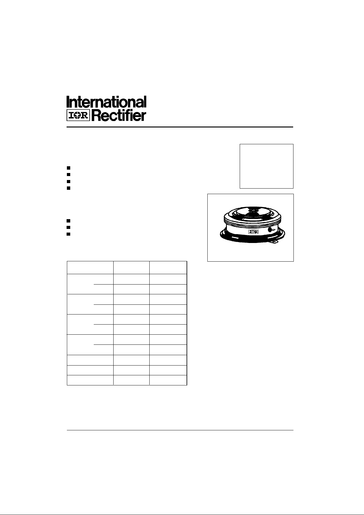
PHASE CONTROL THYRISTORS Hockey Puk Version
ST380C..C SERIES
D-367
Bulletin I25168/B
I
T(AV)
960 A
@ T
hs
55 °C
I
T(RMS)
1900 A
@ T
hs
25 °C
I
TSM
@ 50Hz 15000 A
@ 60Hz 15700 A
I
2
t @ 50Hz 1130 KA2s
@ 60Hz 1030 KA
2
s
V
DRM/VRRM
400 to 600 V
t
q
typical 100 µs
T
J
- 40 to 125 °C
Parameters ST380C..C Units
Major Ratings and Characteristics
Typical Applications
DC motor controls
Controlled DC power supplies
AC controllers
Features
Center amplifying gate
Metal case with ceramic insulator
International standard case TO-200AB (E-PUK)
Low profile hockey-puk to increase current-carrying capability
case style TO-200AB (E-PUK)
Page 3
ST380C..C Series
2222222222222
12
D-368
ELECTRICAL SPECIFICATIONS
Voltage Ratings
Voltage V
DRM/VRRM
, max. repetitive V
RSM
, maximum non- I
DRM/IRRM
max.
Type number Code peak and off-state voltage repetitive peak voltage
@ TJ = TJ max
V V mA
04 400 500
06 600 700
I
T(AV)
Max. average on-state current 960 (440) A 180° conduction, half sine wave
@ Heatsink temperature 55 (75) °C double side (single side) cooled
I
T(RMS)
Max. RMS on-state current 1900 DC @ 25°C heatsink temperature double side cooled
I
TSM
Max. peak, one-cycle 15000 t = 10ms No voltage
non-repetitive surge current 15700 A t = 8.3ms reapplied
12600 t = 10ms 100% V
RRM
13200 t = 8.3ms reapplied Sinusoidal half wave,
I
2
t Maximum I2t for fusing 1130 t = 10ms No voltage Initial TJ = TJ max.
1030 t = 8.3ms reapplied
800 t = 10ms 100% V
RRM
725 t = 8.3ms reapplied
I
2
√t Maximum I2√t for fusing 11300 KA2√s t = 0.1 to 10ms, no voltage reapplied
V
T(TO)
1
Low level value of threshold
voltage
V
T(TO)
2
High level value of threshold
voltage
r
t1
Low level value of on-state
slope resistance
r
t2
High level value of on-state
slope resistance
V
TM
Max. on-state voltage 1.60 V Ipk= 3000A, TJ = TJ max, tp = 10ms sine pulse
I
H
Maximum holding current 600
I
L
Typical latching current 1000
0.85 (16.7% x π x I
T(AV)
< I < π x I
T(AV)
), TJ = TJ max.
0.25 (16.7% x π x I
T(AV)
< I < π x I
T(AV)
), TJ = TJ max.
0.24 (I > π x I
T(AV)
),TJ = TJ max.
Parameter ST380C..C Units Conditions
0.88 (I > π x I
T(AV)
),TJ = TJ max.
On-state Conduction
KA2s
V
mΩ
mA TJ = 25°C, anode supply 12V resistive load
di/dt Max. non-repetitive rate of rise Gate drive 20V, 20Ω, t
r
≤ 1µs
of turned-on current T
J
= TJ max, anode voltage ≤ 80% V
DRM
Gate current 1A, dig/dt = 1A/µs
V
d
= 0.67% V
DRM, TJ
= 25°C
I
TM
= 550A, TJ = TJ max, di/dt = 40A/µs, VR = 50V
dv/dt
= 20V/µs, Gate 0V 100Ω, tp = 500µs
Parameter ST380C..C Units Conditions
Switching
1000 A/µs
t
d
Typical delay time 1.0
t
q
Typical turn-off time 100
µs
ST380C..C 50
Page 4

ST380C..C Series
D-372
Fig. 3 - Current Ratings Characteristics Fig. 4 - Current Ratings Characteristics
Fig. 5- On-state Power Loss Characteristics
Fig. 6- On-state Power Loss Characteristics
Fig. 8 - Maximum Non-Repetitive Surge Current
Single and Double Side Cooled
Fig. 7 - Maximum Non-Repetitive Surge Current
Single and Double Side Cooled
Page 5

ST380C..C Series
D-373
Fig. 9 - On-state Voltage Drop Characteristics
Fig. 10 - Thermal Impedance Z
thJ-hs
Characteristics
Fig. 11 - Gate Characteristics
Page 6

ST380C..C Series
23
D-3693333
dv/dt Maximum critical rate of rise of
off-state voltage
I
RRM
Max. peak reverse and off-state
I
DRM
leakage current
Blocking
500 V/µs TJ = TJ max. linear to 80% rated V
DRM
Parameter ST380C..C Units Conditions
50 mA TJ = TJ max, rated V
DRM/VRRM
applied
PGMMaximum peak gate power 10.0 TJ = TJ max, tp ≤ 5ms
P
G(AV)
Maximum average gate power 2.0 TJ = TJ max, f = 50Hz, d% = 50
I
GM
Max. peak positive gate current 3.0 A TJ = TJ max, tp ≤ 5ms
+V
GM
Maximum peak positive
gate voltage
-V
GM
Maximum peak negative
gate voltage
T
J
= - 40°C
mA T
J
= 25°C
T
J
= 125°C
T
J
= - 40°C
V T
J
= 25°C
T
J
= 125°C
I
GD
DC gate current not to trigger 10 mA
Parameter ST380C..C Units Conditions
20
5.0
Triggering
TYP. MAX.
200 100 200
50 -
2.5 -
1.8 3.0
1.1 -
VGDDC gate voltage not to trigger 0.25 V
Max. gate current/voltage not to
trigger is the max. value which
will not trigger any unit with rated
V
DRM
anode-to-cathode applied
T
J
= TJ max
Max. required gate trigger/ current/ voltage are the lowest value
which will trigger all units 12V
anode-to-cathode applied
V
GT
DC gate voltage required
to trigger
I
GT
DC gate current required
to trigger
W
V T
J
= TJ max, tp ≤ 5ms
T
J
Max. operating temperature range -40 to 125
T
stg
Max. storage temperature range -40 to 150
R
thJ-hs
Max. thermal resistance, 0.09 DC operation single side cooled
junction to heatsink 0.04 DC operation double side cooled
R
thC-hs
Max. thermal resistance, 0.02 DC operation single side cooled
case to heatsink 0.01 DC operation double side cooled
F Mounting force, ± 10% 9800 N
(1000) (Kg)
wt Approximate weight 83 g
Parameter ST380C..C Units Conditions
K/W
Thermal and Mechanical Specification
°C
Case style TO - 200AB (E-PUK) See Outline Table
K/W
Page 7

ST380C..C Series
2222222222222
12
D-370
1 - Thyristor
2 - Essential part number
3 - 0 = Converter grade
4 - C = Ceramic Puk
5 - Voltage code: Code x 100 = V
RRM
(See Voltage Rating Table)
6 - C = Puk Case TO-200AB (E-PUK)
7 - 0 = Eyelet terminals (Gate and Auxiliary Cathode Unsoldered Leads)
1 = Fast-on terminals (Gate and Auxiliary Cathode Unsoldered Leads)
2 = Eyelet terminals (Gate and Auxiliary Cathode Soldered Leads)
3 = Fast-on terminals (Gate and Auxiliary Cathode Soldered Leads)
8 - Critical dv/dt: None = 500V/µsec (Standard selection)
L = 1000V/µsec (Special selection)
Ordering Information Table
∆R
thJ-hs
Conduction
(The following table shows the increment of thermal resistence R
thJ-hs
when devices operate at different conduction angles than DC)
Device Code
51 2
3 4
ST 38 0 C 06 C 1
7
6
8
Single Side Double Side Single Side Double Side
180° 0.010 0.011 0.007 0.007 T
J
= TJ max.
120° 0.012 0.012 0.012 0.013
90° 0.015 0.015 0.016 0.017 K/W
60° 0.022 0.022 0.023 0.023
30° 0.036 0.036 0.036 0.037
Sinusoidal conduction Rectangular conduction
Conduction angle Units Conditions
Page 8

ST380C..C Series
23
D-3713333
Outline Table
Fig. 2 - Current Ratings Characteristics
Fig. 1 - Current Ratings Characteristics
Case Style TO-200AB (E-PUK)
All dimensions in millimeters (inches)
DIA. MAX.
4.75 (0.19)
28 (1.10)
6.5 (0.26)
0.3 (0.01) MIN.
0.3 (0.01) MIN.
ANODE TO GATE
CREEPAGE DISTANCE: 11.18 (0.44) MIN.
STRIKE DISTANCE: 7.62 (0.30) MIN.
25.3 (0.99)
14.1 / 15.1
(0.56 / 0.59)
25°± 5°
GATE TERM. FOR
1.47 (0.06) DIA.
PIN RECEPTACLE
25.3 (0.99)
40.5 (1.59) DIA. MAX.
DIA. MAX.
2 HOLES 3.56 (0.14) x
1.83 (0.07) MIN. DEEP
42 (1.65) MAX.
 Loading...