

Page 1
查询ST330C..L SERIES供应商
PHASE CONTROL THYRISTORS Hockey Puk Version
Bulletin I25154 rev. C 04/00
ST330C..L SERIES
Features
Center amplifying gate
Metal case with ceramic insulator
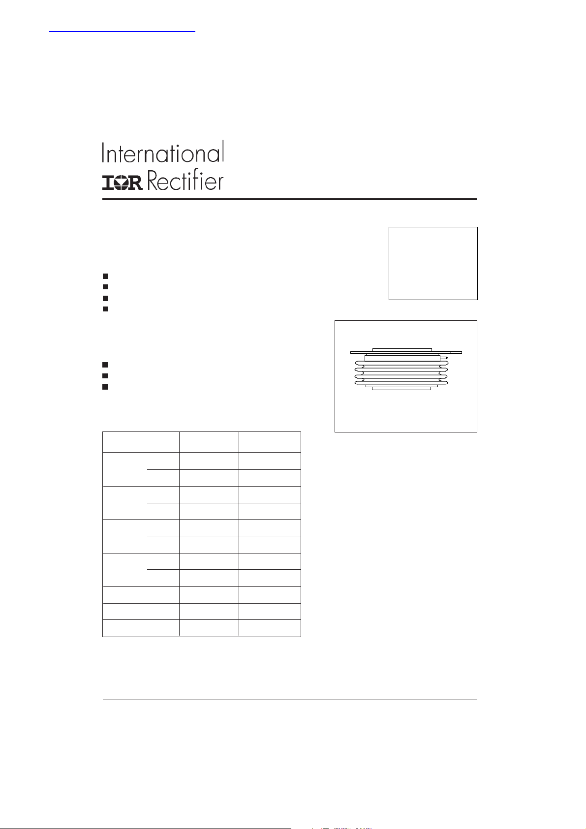
International standard case TO-200AC (B-PUK)
High profile hockey-puk
Typical Applications
DC motor controls
Controlled DC power supplies
AC controllers
Major Ratings and Characteristics
Parameters ST330C..L Units
I
T(AV)
I
T(RMS)
I
TSM
@ T
hs
@ T
hs
@ 50Hz 9000 A
@ 60Hz 9420 A
650 A
55 °C
1230 A
25 °C
650A
case style TO-200AC (B-PUK)
I2t@
V
DRM/VRRM
t
q
T
J
50Hz 405 KA2s
@ 60Hz 370 KA
typical 100 µs
www.irf.com
400 to 1600 V
- 40 to 125 °C
2
s
1
Page 2
ST330C..L Series
Bulletin I25154 rev. C 04/00
ELECTRICAL SPECIFICATIONS
Voltage Ratings
Voltage V
DRM/VRRM
Type number Code peak and off-state voltage repetitive peak voltage @ T
04 400 500
08 800 900
ST330C..L 12 1200 1300 50
14 1400 1500
16 1600 1700
On-state Conduction
Parameter ST330C..L Units Conditions
I
Max. average on-state current 650 (314) A 180° conduction, half sine wave
T(AV)
@ Heatsink temperature 55 (75) °C double side (single side) cooled
Max. RMS on-state current 1230 DC @ 25°C heatsink temperature double side cooled
I
T(RMS)
I
Max. peak, one-cycle 9000 t = 10ms No voltage
TSM
non-repetitive surge current 9420 A t = 8.3ms reapplied
2
I
t Maximum I2t for fusing 405 t = 10ms No voltage Initial TJ = TJ max.
2
I
√t Maximum I2√t for fusing 4050 KA2√s t = 0.1 to 10ms, no voltage reapplied
Low level value of threshold
V
T(TO)1
voltage
High level value of threshold
V
T(TO)2
voltage
r
Low level value of on-state
t1
slope resistance
High level value of on-state
r
t2
slope resistance
V
Max. on-state voltage 1.90 V Ipk= 1730A, TJ = TJ max, tp = 10ms sine pulse
TM
I
Maximum holding current 600
H
I
Typical latching current 1000
L
, max. repetitive V
, maximum non- I
RSM
DRM/IRRM
VVmA
7570 t = 10ms 100% V
7920 t = 8.3ms reapplied Sinusoidal half wave,
370 t = 8.3ms reapplied
287 t = 10ms 100% V
KA2s
262 t = 8.3ms reapplied
0.91 (16.7% x π x I
V
0.93 (I > π x I
T(AV)
0.57 (16.7% x π x I
mΩ
0.57 (I > π x I
mA T
T(AV)
= 25°C, anode supply 12V resistive load
J
RRM
RRM
< I < π x I
T(AV)
),TJ = TJ max.
< I < π x I
T(AV)
),TJ = TJ max.
), TJ = TJ max.
T(AV)
), TJ = TJ max.
T(AV)
max.
= TJ max
J
Switching
Parameter ST330C..L Units Conditions
di/dt Max. non-repetitive rate of rise Gate drive 20V, 20Ω, tr ≤ 1µs
of turned-on current T
Typical delay time 1.0
t
d
Typical turn-off time 100
t
q
1000 A/µs
µs
= TJ max, anode voltage ≤ 80% V
J
Gate current 1A, dig/dt = 1A/µs
= 0.67% V
V
d
I
= 550A, TJ = TJ max, di/dt = 40A/µs, VR = 50V
TM
= 20V/µs, Gate 0V 100Ω, tp = 500µs
dv/dt
DRM, TJ
= 25°C
2
DRM
www.irf.com
Page 3
Blocking
Parameter ST330C..L Units Conditions
dv/dt Maximum critical rate of rise of
off-state voltage
I
Max. peak reverse and off-state
RRM
leakage current
I
DRM
500 V/µs TJ = TJ max. linear to 80% rated V
50 mA TJ = TJ max, rated V
Triggering
Parameter ST330C..L Units Conditions
PGMMaximum peak gate power 10.0 TJ = TJ max, tp ≤ 5ms
P
Maximum average gate power 2.0 TJ = TJ max, f = 50Hz, d% = 50
G(AV)
Max. peak positive gate current 3.0 A TJ = TJ max, tp ≤ 5ms
I
GM
+V
Maximum peak positive
GM
gate voltage
Maximum peak negative
-V
GM
gate voltage
20
5.0
TYP. MAX.
I
DC gate current required
GT
to trigger
200 -
100 200
50 -
V
DC gate voltage required
GT
to trigger
I
DC gate current not to trigger 10 mA
GD
2.5 -
1.8 3.0
1.1 -
VGDDC gate voltage not to trigger 0.25 V
W
= TJ max, tp ≤ 5ms
VT
J
T
= - 40°C
J
= 25°C
mA T
J
TJ = 125°C
TJ = - 40°C
VTJ = 25°C
T
= 125°C
J
= TJ max
T
J
ST330C..L Series
Bulletin I25154 rev. C 04/00
DRM
applied
DRM/VRRM
Max. required gate trigger/ current/ voltage are the lowest value
which will trigger all units 12V
anode-to-cathode applied
Max. gate current/voltage not to
trigger is the max. value which
will not trigger any unit with rated
anode-to-cathode applied
V
DRM
Thermal and Mechanical Specification
Parameter ST330C..L Units Conditions
TJMax. operating temperature range -4 0 to 125
Max. storage temperature range - 40 to 1 50
T
stg
R
Max. thermal resistance, 0.11 DC operation single side cooled
thJ-hs
junction to heatsink 0.06 DC operation double side cooled
Max. thermal resistance, 0.011 DC operation single side cooled
R
thC-hs
case to heatsink 0.005 DC operation double side cooled
F Mounting force, ± 10% 9800 N
(1000) (Kg)
wt Approximate weight 250 g
Case style TO - 200AC (B-PUK) See Outline Table
°C
K/W
K/W
www.irf.com
3
Page 4

ST330C..L Series
Bulletin I25154 rev. C 04/00
∆R
Conduction
thJ-hs
(The following table shows the increment of thermal resistence R
Conduction angle Units Conditions
180° 0.012 0.010 0.008 0.008 T
120° 0.014 0.015 0.014 0.014
90° 0.018 0.018 0.019 0.019 K/W
60° 0.026 0.027 0.027 0.028
30° 0.045 0.046 0.046 0.046
Sinusoidal conduction Rectangular conduction
Single Side Double Side Single Side Double Side
Ordering Information Table
Device Code
ST 33 0 C 16 L 1
when devices operate at different conduction angles than DC)
thJ-hs
J
= TJ max.
3 4
51 2
768
1 - Thyristor
2 - Essential part number
3 - 0 = Converter grade
4 - C = Ceramic Puk
5 - Voltage code: Code x 100 = V
(See Voltage Rating Table)
RRM
6 - L = Puk Case TO-200AC (B-PUK)
7 - 0 = Eyelet terminals (Gate and Auxiliary Cathode Unsoldered Leads)
1 = Fast-on terminals (Gate and Auxiliary Cathode Unsoldered Leads)
2 = Eyelet terminals (Gate and Auxiliary Cathode Soldered Leads)
3 = Fast-on terminals (Gate and Auxiliary Cathode Soldered Leads)
8 - Critical dv/dt: None = 500V/µsec (Standard selection)
L = 1000V/µsec (Special selection)
4
www.irf.com
Page 5

Outline Table
27 (1.06) M AX.
0.7 (0.03) MIN.
0.7 (0.03) MIN.
34 (1.34) DIA. MAX.
TWO PLACES
53 (2.09) DIA. MAX.
6.2 (0.24) MIN.
PIN RECEPTACLE
AMP. 60598-1
ST330C..L Series
Bulletin I25154 rev. C 04/00
4.7 (0.18)
5 8 .5 (2 .3 ) D I A . M A X .
20°± 5°
Case Style TO-200AC (B-PUK)
36.5 (1.44)
2 HOLES DIA. 3.5 (0.14) x
2.5 (0.1) DEEP
CREPAGE DISTANCE 36.33 (1.430) MIN.
STRIKE DISTANCE 17.43 (0.686) MIN.
130
120
110
100
90
80
70
60
50
ST330C..L Series
(Single Side Coo led)
R (D C) = 0.11 K/W
thJ- hs
Conduction Angle
30°
60°
90°
120°
180°
130
120
110
100
40
30
0 50 100 150 200 250 300 350 400 450
Maximum Allowable Heatsink Temperature (°C)
Maxim um Allow able Heatsink Tempe rature (°C)
Average On-state Current (A)
Fig. 1 - Current Ratings Characteristics Fig. 2 - Current Ratings Characteristics
All dimensions in millimeters (inches)
Quote between upper and lower
pole pieces has to be considered
after application of Mounting Force
(see Thermal and Mechanical
Specification)
ST330C ..L Se rie s
(Single Side Cooled)
R (DC ) = 0.11 K /W
thJ-h s
90
80
70
60
50
40
30
20
30°
60°
90°
120°
0 200 400 600 800
Average O n-state Current (A)
Conduction Period
180°
DC
www.irf.com
5
Page 6

ST330C..L Series
Bulletin I25154 rev. C 04/00
130
120
110
ST3 3 0C ..L Se rie s
(Double Side Cooled)
R (DC ) = 0.05 K /W
th J-hs
100
90
80
Conduction Angle
70
60
50
40
30°
60°
90°
120°
30
20
0 200 400 600 800
Maxim um Allowable Heatsink Temperature (° C)
Av erag e O n- state C urre n t (A )
Fig. 3 - Current Ratings Characteristics
1600
1400
1200
1000
180°
120°
90°
60°
30°
800
600
400
200
0
Maximum Average On-state Power Loss (W)
0 100 200 300 400 500 600 700 800
Con ductio n Angle
ST330C..L Series
T = 125°C
J
Average On-state Current (A)
180°
RMS Limit
130
120
110
ST3 3 0C ..L Se rie s
(Do uble Sid e Cooled)
R (DC ) = 0.05 K/W
thJ-h s
100
90
80
Con duction Period
70
30°
60
50
40
30
20
0 200 40 0 600 800 1 000 12 00 1400
Maxim um Allow able Heatsink Tempe rature (° C)
60°
90°
120°
180°
A ve rage O n-state C u rren t (A )
Fig. 4 - Current Ratings Characteristics
2200
2000
1800
1600
1400
1200
DC
180°
120°
90°
60°
30°
RMS Limit
1000
800
Conduction Period
600
400
200
0
Maximum Average On-state Power Loss (W)
0 200 400 600 800 1000 1200 1400
ST330C..L Series
T = 125°C
J
Aver age O n-state Curren t (A)
Fig. 6- On-state Power Loss CharacteristicsFig. 5- On-state Power Loss Characteristics
DC
8000
At Any Rated Load Condition And With
Rated V Applied Following Surge.
7500
7000
6500
RRM
In it ia l T = 1 2 5 ° C
J
@ 60 H z 0.0083 s
@ 50 H z 0.0100 s
6000
5500
5000
4500
ST330C ..L Series
4000
Peak Half Sine Wave On-state Current (A)
3500
1 10 100
Number Of Equa l Amplitude Half Cycle Current Pulses (N)
Fig. 7 - Maximum Non-Repetitive Surge Current
Single and Double Side Cooled
6
9000
M axim um N on Repet itive Surge Current
8500
8000
7500
7000
Versus Pulse Train Dura tion. Con trol
Of Conduction May Not Be Maintained.
Initial T = 125°C
No Voltage Reapplied
Rated V Reapplied
RRM
6500
6000
5500
5000
4500
ST330C..L Series
4000
Peak Half Sine Wave On-state Current (A)
3500
0.01 0.1 1
Pulse Train Duration (s)
Fig. 8 - Maximum Non-Repetitive Surge Current
Single and Double Side Cooled
www.irf.com
J
Page 7

ST330C..L Series
Bulletin I25154 rev. C 04/00
10000
T = 25° C
J
T = 125°C
J
1000
ST3 3 0C ..L Se ries
Instantaneo us On-state Curre nt (A)
100
0.511.52 2.533.544.55 5.566.57
In sta nta ne o us O n -state V o lta g e (V )
Fig. 9 - On-state Voltage Drop Characteristics
1
Stead y Sta te Va lue
R = 0.11 K/W
thJ-h s
thJ-h s
(Single Side Co oled)
R = 0.05 K/W
0.1
thJ-h s
(Dou ble Side Cooled)
(D C O pe ration)
0.001
Transient The rm al Im pedance Z (K/W )
Instan ta n eou s G ate Volta ge (V)
www.irf.com
0.01
ST330C..L Series
0 .00 1 0.0 1 0.1 1 1 0
Squa re W a ve Pulse D uration (s)
Fig. 10 - Thermal Impedance Z
100
Rectangular gate pulse
a) Recomm ended load line for
ra ted di/dt : 20V , 1 0ohm s; tr<=1 µ s
b) Reco m m en d e d loa d line for
<=30% rated d i/dt : 10 V, 10ohm s
10
tr< =1 µs
(b)
Tj=-40 °C
Tj=25 °C
1
VG D
IG D
0.1
0.0 01 0 .0 1 0 .1 1 10 1 00
Tj= 125 °C
Device: ST3 30C..L Series
Instan ta n eous G a te Cu rren t (A)
Characteristics
thJ-hs
(1) PG M = 10W , tp = 4m s
(2) PG M = 20W , tp = 2m s
(3) PG M = 40W , tp = 1m s
(4) PG M = 60W , tp = 0.66m s
(a)
Frequ en c y Lim ited b y P G (AV)
(1)
(2)
(3)
Fig. 11 - Gate Characteristics
(4)
7
 Loading...