

Datasheet ST3243CTR, ST3243CPR, ST3243CDR, ST3243BTR, ST3243BPR Datasheet (SGS Thomson Microelectronics)
...Page 1
ST3243
3 TO 5.5V, 400KBPS, RS-232
TRANSCEIVER WITH AUTO-POWERDOWN
■ 1µA SUPPLY CURRENT ACHIEVED WHEN
IN AUTO-POWERDOWN
■ 250Kbps MINIMUM GUARANTEED DATA
RATE
■ GUARANTEED 6V/µs SLEW RATE RANGE
■ GUARANTEED MOUSE DRI VEABILITY
■ 0.1µF EXTERNAL CAPACITORS
■ MEET EIA/TIA-232 SPECIFICATIONS DOWN
TO 3V
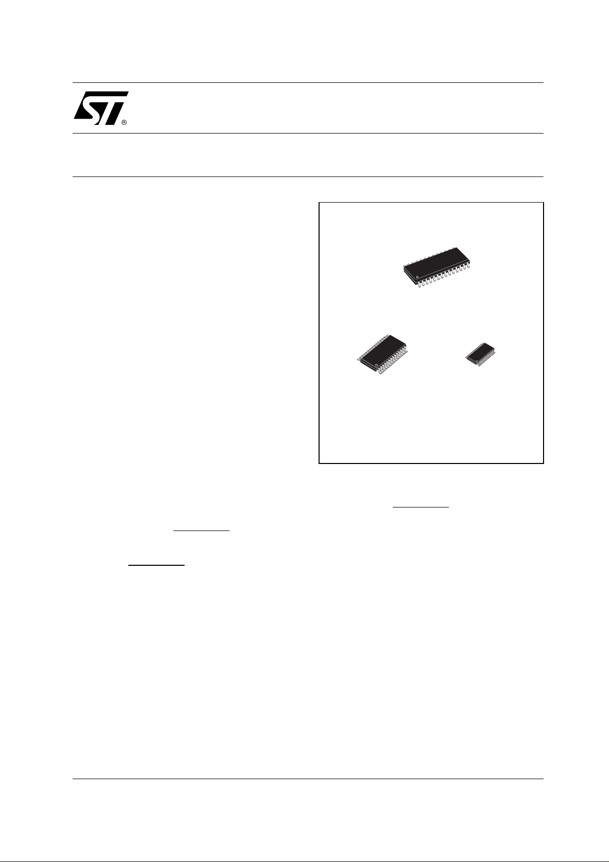
■ A VAILABL E IN SO-28, SSOP-28 AND
TSSOP28
DESCRIPTION
The ST3243 device consists of 3 drivers, 5
receivers and a dual charge-pump circuit. The
device meets the requirements of EIA/TIA and
V.28/V.24 comuni cation standards providing hi gh
data rate capability.
The receiver R2 is always active to implement a
wake-up feature for serial port.
The ST3243 has a proprietary low-dropout
transmitter output stage enabling true RS-232
performance from a 3.0V to 5.5V supply with a
dual charge pump. The device is guaranteed to
run at data rates of 250kbps while maintaining
RS-232 output levels.
The Auto-powerdown feature functions when
FORCEON is low and FORCEOFF
is high. During
this mode of operation, if the device does not
sense a valid RS-232 signal, the driver outputs are
disabled. If FORCEOFF
is set low, both drivers
and receivers (expert R2B) are shut off, and
supply current is reduced to 1mA. Disconnecting
SOP
SSOP
TSSOP
the serial port or turning off the p eripheral drives
causes the auto-powerdown condition to occur.
Auto-powerdown can be disabled when
FORCEON and FORCEOFF
are high, and should
be done when driving a serial mouse. With
Auto-powerdown enable d, the d evice is act ivated
automatically when a valid signal is applied to any
receiver i nput.
Typical application are in notebook, subnot ebook,
palmtop computers, battery-powered equipment,
hand-held equipment, peripherals and printers.
1/11May 2002
Page 2
ST3243
ORDERING CODES
Type
Temperature
Range
Package Comments
ST3243CD 0 to 70 °C SO-28 (Tube) 27parts per tube / 12tube per box
ST3243BD -40 to 85 °C SO-28 (Tube) 27parts per tube / 12tube per box
ST3243CDR 0 to 70 °C SO-28 (Tape & Reel) 1000 parts per reel
ST3243BDR -40 to 85 °C SO-28 (Tape & Reel) 1000 parts per reel
ST3243CPR 0 to 70 °C SSOP-28 (Tape & Reel) 1350 parts per reel
ST3243BPR -40 to 85 °C SSOP-28 (Tape & Reel) 1350 parts per reel
ST3243CTR 0 to 70 °C TSSOP28 (Tape & Reel) 2500 parts per reel
ST3243BTR -40 to 85 °C TSSOP28 (Tape & Reel) 2500 parts per reel
PIN DESCRIPTION
PlN N° SYMBOL NAME AND FUNCTION
+ Positive Terminal of Inverting Charge Pump Capacitor
1
2
3 V- -5.5V Generated by the Charge Pump
4
5
6
7
8
9
10
11
12
13
14
15
16
17
18
19
20
21
22
23
24
25 GND Ground
26
27 V+ 5.5V Generated by the Charge Pump
28
C
2
C
- Negative Terminal of Inverting Charge Pump Capacitor
2
R1
IN
R2
IN
R3
IN
R4
IN
R5
IN
T1
OUT
T2
OUT
T3
OUT
T3
IN
T2
IN
T1
IN
R5
OUT
R4
OUT
R3
OUT
R2
OUT
R1
OUT
R2
OUTB
INVALID
First Receiver Input Voltage
Second Receiver Input Voltage
Third Receiver Input Voltage
Fourth Receiver Input Voltage
Fifth Receiver Input Voltage
First Transmitter Output Voltage
Second Transmitter Output Voltage
Third Transmitter Output Voltage
Third Transmitter Input Voltage
Second Transmitter Input Voltage
First Transmitter Input Voltage
Fifth Receiver Output Voltage
Fourth Receiver Output Voltage
Third Receiver Output Voltage
Second Receiver Output Voltage
First Receiver Output Voltage
Non-inverting Complementary Receiver Output, always active
for wake-up
Output of the valid signal detector. Indicates if a valid RS-232
level is present on receiver inputs logic "1"
FORCEOFF
Drive low to shut down transmitters and on-board power
supply. This over-rides all automatic circuitry and FORCEON
FORCEON Drive high to override automatic circuitry keeping transmitters
on (FORCEOFF
- Negative Terminal of Voltage- Charge Pump Capacitor
C
1
V
CC
+ Positive Terminal of Voltage- Charge Pump Capacitor
C
1
Supply Voltage
must be high)
2/11
Page 3
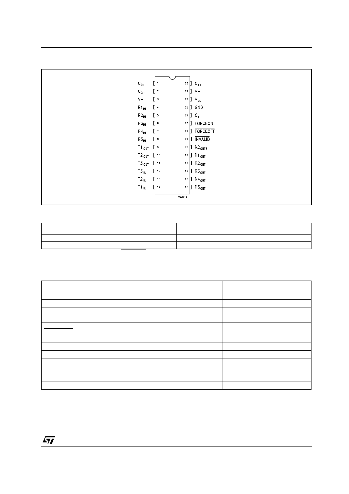
PIN CONFIGURATION
ST3243
TRUTH TABLE
FORCE OFF
T
OUT
R
OUT
0 HIGH Z HIGH Z ACTIVE *
1 ACTIVE * ACTIVE * ACTIVE *
* If the part is in auto-powerdown mode (FORCE OFF = VCC, FORCE ON = GND) it is shutdown , if no valid R S- 232 levels are present on
all receiver input
R
2OUTB
ABSOLUTE MAXIMUM RATINGS
Symbol Parameter Value Unit
V
CC
V+
V- Inverted Voltage Terminal 0.3 to -7 V
V+ +|V-| 13 V
FORCEON,
FORCEOFF,
T
IN
R
IN
T
OUT
R
OUT ROUTB
INVALID
t
SHORT
T
stg
Absolute Maximum Ratings are those values beyond which damage to the device may occur. Functional operation under these condition i s
not implied. V+ and V- can have a maximum magnitude of +7V, but their absolute addition can not exceed 13 V.
(*) The device doesn’t m eet 1KV ESD HBM
Supply Voltage
Doubled Voltage Terminal (V
Input Voltage
Receiver Input Voltage Range
Transmitter Output Voltage Range
Receiver Output Voltage Range
Short Circuit Duration on T
(one at a time)
OUT
Storage Temperature Range
-0.3 to 6 V
-0.3) to 7
CC
-0.3 to 6 V
25 V
±
13.2 V
±
-0.3 to (V
CC
+ 0.3)
Continuous
-65 to 150 °C
V
V
3/11
Page 4
ST3243
ELECTRICAL CHARACTERISTICS
- C4 = 0.1µF, VCC = 3V to 5.5V, TA = -40 to 85°C, unless otherwise specified.
(C
1
Typical values are referred to T
Symbol Parameter Test Conditions Min. Typ. Max. Unit
I
ASHDN
I
SHDN
I
SHDN
Supply Current
Auto-powerdown
Shutdown Supply Current VCC = 3.3 or 5.0V TA = 25°C
Supply Current
Auto-powerdown Disabled
LOGIC INPUT ELECTRICAL CHARACTERISTICS
(C
- C4 = 0.1µF, VCC = 3V to 5.5V, TA = -40 to 85°C, unless otherwise specified.
1
Typical values are referred to T
Symbol Parameter Test Conditions Min. Typ. Max. Unit
V
V
V
V
V
Input Logic Threshold Low T-IN, FORCEON, FORCEOFF 0.8 V
TIL
Input Logic Threshold High T-IN, FORCEON, FORCEOFF
TIH
Transmitter Input
THYS
Hysteresis
I
Input Leakage Current T-IN, FORCEON, FORCEOFF ±
IL
I
Output Leakage Current Receiver Disabled
OL
Output Voltage Low I
OL
Output Voltage High I
OH
= 25°C)
A
VCC = 3.3 or 5.0V TA = 25°C
All R_IN open FORCEOFF
All R_IN open FORCEOFF
VCC = 3.3 or 5.0V TA = 25°C
FORCEON = FORCEOFF
= 25°C)
A
VCC = 3.3V
V
= 5V
CC
= 1.6mA 0.4 V
OUT
= -1mA VCC-0.6 VCC-0.1 V
OUT
= V
CC
= GND
= VCCNo Load
2
2.4
110
110
0.3 1 mA
0.5 V
±
0.01
0.05
1.0
±
10
±
A
µ
A
µ
V
V
A
µ
A
µ
AUTO-POWERDOWN ELECTRICAL CHARACTERISTICS
(C
- C4 = 0.1µF, VCC = 3V to 5.5V, TA = -40 to 85°C, unless otherwise specified.
1
Typical values are referred to T
Symbol Parameter Test Conditions Min. Typ. Max. Unit
V
V
V
V
t
t
Receiver Input Threshold to
RITE
Transmitter Enabled
Receiver Input Threshold to
RITD
Transmitter Disabled
INVALID Output Voltage
IOL
LOW
INVALID Output Voltage
IOH
HIGH
Receiver Threshold to
t
WU
Transmitter Enabled
Receiver Positive or
invh
Negative Threshold to
INVALID
Receiver Positive or
invL
Negative Threshold to
INVALID
HIGH
LOW
= 25°C)
A
Positive Threshold
2.7 V
Negative Threshold 2.7
1µA Supply Current -0.3 0.3 V
0.4 V
VCC-0.6 V
I
= 1.6mA 250
OUT
I
= -1mA 1
OUT
30
V
s
µ
s
µ
s
µ
4/11
Page 5

ST3243
TRANSMITTER ELECTRICAL CHARACTERISTICS
- C4 = 0.1µF, VCC = 3V to 5.5V, TA = -40 to 85°C, unless otherwise specified.
(C
1
Typical values are referred to T
Symbol Parameter Test Conditions Min. Typ. Max. Unit
V
R
V
Output Voltage Swing All Transmitter outputs are loaded with
TOUT
Output Resistance VCC = V+ = V- = 0V V
OUT
I
Output Short Circuit Current
SC
Transmitter Output Voltage T1IN = T2IN = GND, T3IN = V
OT
RECEIVER ELECTRICAL CHARACTERISTICS
(C
- C4 = 0.1µF, VCC = 3V to 5.5V, TA = -40 to 85°C, unless otherwise specified.
1
Typical values are referred to T
Symbol Parameter Test Conditions Min. Typ. Max. Unit
V
V
V
V
RIHYS
R
Receiver Input Voltage
RIN
Operating Range
RS-232 Input Threshold
RIL
Low
RS-232 Input Threshold
RIH
High
Input Hysteresis 0.5 V
Input Resistance TA = 25°C 3 5 7 K
RIN
= 25°C)
A
3KΩ to GND
OUT
T3OUT loaded with 3KΩ to GND
T1OUT and T2OUT loaded with 2.5mA
each
= 25°C)
A
TA = 25°C VCC = 3.3V
T
= 25°C VCC = 5.0V
A
TA = 25°C VCC = 3.3V
T
= 25°C VCC = 5.0V
A
5
±
5.4 V
±
= ± 2V 300 10M
35
±
5V
CC
±
-25 25 V
0.6
0.8
1.2
1.2
1.5
1.8
60 mA
±
2.4
2.4
Ω
V
V
Ω
TIMING CHARACTERISTICS
(C
- C4 = 0.1µF, VCC = 3V to 5.5V, TA = -40 to 85°C, unless otherwise specified.
1
Typical values are referred to T
Symbol Parameter Test Conditions Min. Typ. Max. Unit
D
Maximum Data Rate RL = 3K
R
t
t
T_SKEW
t
R_SKEW
t
t
S
Receiver Propagation Delay RIN to R
PHL
t
PLH
Transmitter Skew 100 ns
Receiver Skew 50 ns
Receiver Positive or
INVH
negative Threshold to
INVALID
Receiver Positive or
INVL
negative Threshold to
INVALID
Transition Slew Rate TA = 25°C RL = 3K to 7K
RT
HIGH
LOW
= 25°C)
A
CL= 1000pF
Ω
one trasmitter switching
OUT
CL = 150pF 0.15
Ω
measured from +3V to -3V or -3V to +3V
C
= 150pF to 1000pF
L
C
= 150pF to 2500pF
L
VCC = 3.3V
250 400 Kbps
1
30
6
4
30
30
V/µs
V/µs
s
µ
s
µ
s
µ
5/11
Page 6

ST3243
APPLICATION CIRCUITS
CAPACITANCE VALUE (µF)
V
CC
3.0 to 3.6 0.1 0.1 0.1 0.1 0.1
4.5 to 5.5 0.047 0.33 0.33 0.33 0.33
3.0 to 5.5 0.22 1.0 1.0 1.0 0.22
6/11
C1 C2 C3 C4 Cbypass
Page 7

TYPICAL PERFORMANCE CHARACTERISTICS (unless otherwise specified Tj = 25°C)
Figure 1 : INVALID HIGH Threshold Time
Figure 4 : TReceiver Output Enab le & Disable
Time
ST3243
Figure 2 : INVALID LOW Threshold Time
Figure 3 : Receiver Propagation Delay
Figure 5 : Output Current vs Output High Voltage
Figure 6 : Output Current vs Output Low Voltage
7/11
Page 8

ST3243
SO-28 MECHANICAL DATA
DIM.
MIN. TYP MAX. MIN. TYP. MAX.
A 2.65 0.104
a1 0.1 0.3 0.004 0.012
b 0.35 0.49 0.014 0.019
b1 0.23 0.32 0.009 0.012
C 0.5 0.020
c1 45° (typ.)
D 17.70 18.10 0.697 0.713
E 10.00 10.65 0.393 0.419
e 1.27 0.050
e3 16.51 0.650
F 7.40 7.60 0.291 0.300
L 0.50 1.27 0.020 0.050
S8° (max.)
mm. inch
8/11
0016023
Page 9

ST3243
SSOP28 MECHANICAL DATA
mm. inch
DIM.
MIN. TYP MAX. MIN. TYP. MAX.
A 2 0.079
A1 0.050 0.002
A2 1.65 1.75 1.85 0.065 0.069 0.073
b 0.22 0.38 0.009 0.015
c 0.09 0.25 0.004 0.010
D 9.9 10.2 10.5 0.390 0.402 0.413
E 7.4 7.8 8.2 0.291 0.307 0.323
E1 5 5.3 5.6 0.197 0.209 0.220
e 0.65 BSC 0.0256 BSC
K 0° 10° 0° 10°
L 0.55 0.75 0.95 0.022 0.030 0.037
9/11
Page 10

ST3243
TSSOP28 MECHANICAL DATA
mm. inch
DIM.
MIN. TYP MAX. MIN. TYP. MAX.
A 1.2 0.047
A1 0.05 0.15 0.002 0.004 0.006
A2 0.8 1 1.05 0.031 0.039 0.041
b 0.19 0.30 0.007 0.012
c 0.09 0.20 0.004 0.0089
D 9.6 9.7 9.8 0.378 0.382 0.386
E 6.2 6.4 6.6 0.244 0.252 0.260
E1 4.3 4.4 4.48 0.169 0.173 0.176
e 0.65 BSC 0.0256 BSC
K0° 8°0° 8°
L 0.45 0.60 0.75 0.018 0.024 0.030
10/11
0128292B
Page 11

ST3243
Information furnished is believed to be accurate and reliable. However, STMicroelectronics assumes no responsibility f or t he
consequences of use of such informatio n nor for any infringement of paten ts or o ther rig hts of t hird part ies which ma y result from
its use. No license is granted by implication or otherwise under any patent or patent rights of STMicroelectronics. Specifications
mentioned in this publication are subject to change without notice. This publication supersedes and replaces all information
previousl y suppl ied. STM icroel ectronics produc ts are not auth orized for use as c ritica l compone nts in l ife s upport dev ices or
systems without express written approval of STMicroelectronics.
Australia - Brazil - Canada - China - Finland - France - Germany - Hong Kong - India - Israel - Italy - Japan - Malaysia - Malta - Morocco
© The ST logo is a registered trademark of STMicroelectronics
© 2002 STMicroelectronics - Printed in Italy - All Rights Reserved
STMicroelectronics GROUP OF COMPANIES
Singapore - Spain - Sweden - Switzerland - United Kingdom - United States.
© http://www.st.com
11/11
 Loading...