

Datasheet ST3222ECTR, ST3222ECPR, ST3222ECDR, ST3222ECD, ST3222EBTR Datasheet (SGS Thomson Microelectronics)
...Page 1
±15KV ESD-PROTECTED, 3 TO 5.5V, LOW P OWER,
UP T O 250KBPS, RS-232 DRIVERS AND RECEIVERS
■ ESD PROTECTIO FOR RS-232I/O PINS
±15KV HUMAN BODY MO DEL
±8KV IEC 1000-4-2 CONTACT DISCHARGE
■ 300µA SUPP LY CURRENT
■ 250Kbps MINIMUM GUARENTEED DATA
RATE
■ 6V/µs MINIMUM GUARANTEED SLEW RATE
■ MEET EIA/TIA-232 SPECIFICATIONS DOWN
TO 3V
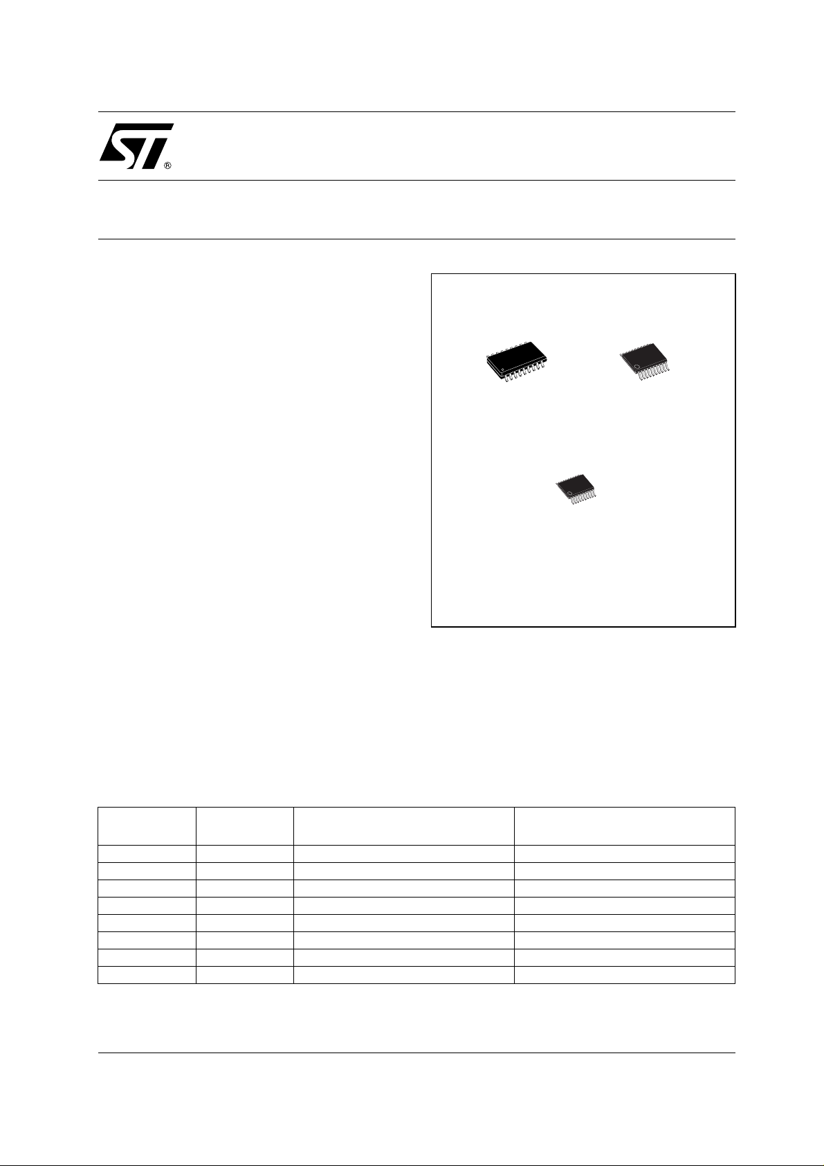
■ AVAILABLEIN SO-18, SSOP20 AND
TSSOP20
DESCRIPTION
The ST3222E is a 3V p owered EIA/TIA-23 2 and
V.28/V.24 communications interface with low
power requirements, high data-rate capabilities
and enhanced electrostatic discharge (ESD)
protection to ±8kV using IEC1000-4-2 Contact
Discharge and ±15kV using the Human Body
Model. ST3222E has a proprietary low dropout
transmitter output stage providing true RS-232
performance from 3 to 5V supplies with a dual
charge pump. The charge pump requires only four
small 0.1mF external capacitors for operation form
3V supply.
The dev ice has two receivers and two drivers. The
ST3222E features a 1µA shutdown mode that
reduces power consumption and extends battery
life in port able systems. Its receivers can remain
active in shutdown mode, allowing external
ST3222E
SOP SSOP
TSSOP
devices such as modems to be monitored using
only1µA supply current.
The device is guaranteed to run at data rates of
250Kbps while maintaining RS-232 output levels.
Typical applications are Notebook, Subnotebook
and Palmtop Computers, Battery Powered
Equipment, Hand-Held Equipment, Peripherals
and Printers.
ORDERING CODES
Type
ST3222ECD 0 to 70 °C SO-18 (Tube) 50parts per tube / 20tube per box
ST3222EBD -40 to 85 °C SO-18 (Tube) 50parts per tube / 20tube per box
ST3222ECDR 0 to 70 °C SO-18 (Tape & Reel) 1000 parts per reel
ST3222EBDR -40 to 85 °C SO-18 (Tape & Reel) 1000 parts per reel
ST3222ECPR 0 to 70 °C SSOP20 (Tape & Reel) 1350 parts per reel
ST3222EBPR -40 to 85 °C SSOP20 (Tape & Reel) 1350 parts per reel
ST3222ECTR 0 to 70 °C TSSOP20 (Tape & Reel) 2500 parts per reel
ST3222EBTR -40 to 85 °C TSSOP20 (Tape & Reel) 2500 parts per reel
Temperature
Range
Package Comments
1/10March 2003
Page 2

ST3222E
PIN CONFIGURATION
PIN DESCRIPTION
SO-18 SSOP20/TSSOP20
PlN N°
(SO-18)
11EN
PlN N°
(SSOP20 TSSP20)
SYMBOL NAME AND FUNCTION
Receiver Enable Control. Drive low for normal
operation. Drive high to force the receivers outputs
(R_OUT) into a high-impedance state.
22
+
C
1
Positive Terminal for the first Charge Pump
Capacitor
3 3 V+ 5.5V Generated By The Charge Pump.
44
55
66
-
C
1
+
C
2
-
C
2
Negative Terminal for the first Charge Pump
Capacitor
Positive Terminal for the second Charge Pump
Capacitor
Negative Terminal for the second Charge Pump
Capacitor
7 7 V- -5.5V Generated By The Charge Pump.
88
99
10 10
T2
R2
R2
OUT
IN
OUT
Second Transmitter Output Voltage
Second Receiver Input Voltage
Second Receiver Output Voltage
11 NC Not Connected
11 12
12 13
T2
T1
IN
IN
Second Transmitter Input Voltage
First Transmitter Input Voltage
14 NC Not Connected
13 15
14 16
15 17
R1
T1
R1
OUT
IN
OUT
First Receiver Output Voltage
First Receiver Input Voltage
First Transmitter Output Voltage
16 18 GND Ground
17 19
V
CC
18 20 SHDN
Supply Voltage
Active Low Shutdown Control Input. Drive Low To
Shut-down Transmittes And Charge Pump
2/10
Page 3
ST3222E
ABSOLUTE MAXIMUM RATINGS
Symbol Parameter Value Unit
V
V+
V- Inverted Voltage Terminal 0.3 to -7 V
V+ +|V-| 13 V
T
SHDN
R
T
OUT
R
OUT
t
SHORT
Absolute Maximum Ratings are those values beyond which damage to the device may occur. Functional operation under these condition is
not implied. V+ and V- can have a maximum magnitude of +7V, but their absolute addition can not exceed 13 V.
SHUTDOWN AND ENABLE CONTROL TRUTH TABLE
Supply Voltage
CC
Doubled Voltage Terminal (V
Transmitter Input Voltage Range
IN
-0.3 to 6 V
-0.3)to7
CC
-0.3 to 6 V
Transmitter Input Voltage Range -0.3 to 6 V
Receiver Input Voltage Range
IN
Transmitter Output Voltage Range
± 25 V
± 13.2 V
Receiver Output Voltage Range -0.3 to (VCC+ 0.3)
Transmitter Output Short to GND Time
Continuous
V
V
SHDN
EN T-OUT R-OUT
0 0 High Z Active
0 1 High Z High Z
1 0 Active Active
1 1 Active High Z
ESD PERFORMANCE: TRANSMITTER OUTPUTS, RECEIVER INPUTS
Symbol Parameter Test Conditions Min. Typ. Max. Unit
ESD ESD Protection Voltage Human Body Model ±15 kV
ESD ESD Protection Voltage IEC-1000-4-2 ±8kV
ELECTRICAL CHARACTERISTICS
(C
Typical values are referred to T
Symbol Parameter Test Conditions Min. Typ. Max. Unit
I
SUPPLYVCC
=0.1µF, VCC=3Vto5.5V,TA= -40 to 85°C, unless otherwise specified.
1-C4
=25°C)
A
Power Supply Current No Load SHDN=VCCTA= 25°C 0.3 1 mA
I
SHDN
SHUTDOWN Supply
Current
No Load SHDN=VCCTA= 25°C 1 10 µA
LOGIC INPUT E L ECTRICAL CHARACTERISTICS
(C
Typical values are referred to T
Symbol Parameter Test Conditions Min. Typ. Max. Unit
Note 1: Transmitter input hysteresis is typically 250mV
=0.1µF, VCC=3Vto5.5V,TA= -40 to 85°C, unless otherwise specified.
1-C4
V
IL
V
IH
V
HYS
I
IL
Input Logic Threshold Low T-IN, EN, SHDN (Note 1) 0.8 V
Input Logic Threshold High VCC= 3.3V 2 V
Transmitter Input
Histeresys
Input Leakage Current T-IN, EN, SHDN ± 0.01 ± 1 µA
=25°C)
A
V
=5V 2.4
CC
0.25 V
3/10
Page 4

ST3222E
TRANSMITTER ELECTRICAL CHARACTERISTICS
(C
Typical values are referred to T
Symbol Parameter Test Conditions Min. Typ. Max. Unit
V
R
RECEIVER ELECTRICAL CHARACTERISTICS
(C
Typical values are referred to T
Symbol Parameter Test Conditions Min. Typ. Max. Unit
V
=0.1µFVCC=3Vto5.5V,TA= -40 to 85°C, unless otherwise specified.
1-C4
=25°C)
A
Output Voltage Swing All Transmitter outputs are loaded with
TOUT
TOUT
I
TSC
I
TOL
Transmitter Output
Resistance
Output Short Circuit Current ± 60 mA
Output Leakage Current VCC= 0V or 3V to 3.6V V
3KΩ to GND
VCC=V+=V-=0V V
= ± 2V 300 10M Ω
OUT
= ± 12V
OUT
Transmitters Disable
=0.1µFVCC=3Vto5.5V,TA= -40 to 85°C, unless otherwise specified.
1-C4
I
OL
V
RIN
V
RIL
V
RIH
RIHYS
R
RIN
V
ROL
V
ROH
Output Leakage Current R-OUT, EN =VCC, Receiver Disabled ± 0.05 ± 10 µA
Receiver Input Voltage
Operating Range
Input Threshold Low TA= 25°C VCC= 3.3V 0.6 1.2 V
Input Threshold High TA= 25°C VCC= 3.3V 1.5 2.4 V
Input Hysteresis 0.5 V
Input Resistance TA= 25°C 3 5 7 KΩ
Output Voltage Low I
Output Voltage High I
=25°C)
A
= 25°C VCC= 5V 0.8 1.5
T
A
= 25°C VCC= 5V 1.8 2.4
T
A
= 1.6mA 0.4 V
OUT
= -1mA VCC-0.6 VCC-0.1 V
OUT
± 5 ± 5.4 V
± 25 µA
-25 25 V
TIMING CHARACTERISTICS
(C
Typical values are referred to T
Symbol Parameter Test Conditions Min. Typ. Max. Unit
-t
|t
-t
(Note 1) Transmitter Skew is measured at the transmitter zero cross points
4/10
=0.1µF, VCC=3Vto5.5V,TA= -40 to 85°C, unless otherwise specified.
1-C4
=25°C)
A
Data Transfer Rate RL=3KΩ CL2= 1000pF
D
R
one trasmitter switching
t
PHLR
t
PLHR
|t
PHLT
THL
t
OER
t
ODR
PHLR
THR
S
Propagation Delay Input to
Output
Transmitter Propagation
Delay Difference
|
Receiver Output Enable
Time
Receiver Output Disable
Time
Receiver Propagation Delay
Difference
|
Trnasition Slew Rate TA= 25°C RL=3KΩto 7KΩ VCC= 3.3V
RT
R
XIN
to R
XOUT
CL= 150pF 0.15 µs
(Note 1) 200 ns
Normal Operation 50 ns
Normal Operation 50 ns
measured from +3V to -3V or -3V to +3V
= 150pF to 1000pF
C
L
C
= 150pF to 2500pF
L
250 Kbps
50 ns
6
4
30
30
V/µs
V/µs
Page 5

APPLICATION CIRCUITS
ST3222E
CAPACITANCE VALUE (µF)
V
CC
3.0 to 3.6 0.1 0.1 0.1 0.1 0.1
4.5 to 5.5 0.047 0.33 0.33 0.33 0.1
3.0 to 5.5 0.1 0.47 0.47 0.47 0.1
C1 C2 C3 C4 Cbypass
5/10
Page 6

ST3222E
TYPICAL PERFORMANCE CHARACTERISTICS (unless otherwise specified Tj= 25°C)
Figure 1 : Output Current vs Output High Voltage
Figure 4 : Output Current vs Output Low Voltage
Figure 2 : Output Current vs Output High Voltage
Figure 3 : Output Current vs Output Low Voltage
Figure 5 : Voltage Transfer Characteristics
for Trasmitter Inputs
Figure 6 : Receiver Input Resistance
6/10
Page 7

SO-18 MECHANICAL DATA
ST3222E
DIM.
MIN. TYP MAX. MIN. TYP. MAX.
A 2.35 2.65 0.092 0.104
A1 0.1 0.3 0.004 0.012
A2 2.55 0.100
B 0.33 0.51 0.013 0.020
C 0.23 0.32 0.009 0.012
D 11.35 11.75 0.447 0.462
E 7.4 7.6 0.291 0.299
e 1.27 0.050
H 10.00 10.65 0.393 0.419
h 0.25 0.75 0.010 0.029
k8 ˚ (max.)
L 0.4 1.27 0.016 0.050
mm. inch
Be
0.10mm
.004
Seating Plane
D
1018
19
A2
h x 45û
A
K
L
A1 C
H
E
SO18
0070768
7/10
Page 8

ST3222E
SSOP20 MECHANICAL DATA
mm. inch
DIM.
MIN. TYP MAX. MIN. TYP. MAX.
A 2 0.079
A1 0.05 0.002
A2 1.65 1.75 1.85 0.065 0.069 0.073
b 0.22 0.38 0.009 0.015
c 0.09 0.25 0.004 0.010
D 6.9 7.2 7.5 0.272 0.283 0.295
E 7.4 7.8 8.2 0.291 0.307 0.323
E1 5 5.3 5.6 0.197 0.209 0.220
e 0.65 BSC 0.0256 BSC
K0˚4˚8˚0˚4˚8˚
L 0.55 0.75 0.95 0.022 0.030 0.037
A2
A
A1
b
e
K
c
L
E
D
E1
PIN 1 IDENTIFICATION
8/10
1
0061436C
Page 9

ST3222E
TSSOP20 MECHANICAL DATA
mm. inch
DIM.
MIN. TYP MAX. MIN. TYP. MAX.
A 1.2 0.047
A1 0.05 0.15 0.002 0.004 0.006
A2 0.8 1 1.05 0.031 0.039 0.041
b 0.19 0.30 0.007 0.012
c 0.09 0.20 0.004 0.0079
D 6.4 6.5 6.6 0.252 0.256 0.260
E 6.2 6.4 6.6 0.244 0.252 0.260
E1 4.3 4.4 4.48 0.169 0.173 0.176
e 0.65 BSC 0.0256 BSC
K0˚ 8˚0˚ 8˚
L 0.45 0.60 0.75 0.018 0.024 0.030
A2
A
A1
b
e
K
c
L
E
D
E1
PIN 1 IDENTIFICATION
1
0087225C
9/10
Page 10

ST3222E
Information furnished is believed to be accurate and reliable. However, STMicroelectronics assumes no responsibility for the
consequences of use o f suc h inf ormat ion n or f or an y infr ingeme nt of paten ts or oth er ri gh ts of third part ies whic h may resul t f rom
its use. No license is granted by implication or otherwise under any patent or patent rights of STMicroelectronics. Specifications
mentioned in this publication are subject to change without notice. This publication supersedes and replaces all information
previously supplied. STMicroelectronics products are not authorized for use as critical components in life support devices or
systems without express written approval of STMicroelectronics.
Australia - Brazil - Canada - China - Finland - France - Germany - Hong Kong - India - Israel - Italy - Japan - Malaysia - Malta - Morocco
© The ST logo is a registered trademark of STMicroelectronics
© 2003 STMicroelectronics - Printed in Italy - All Rights Reserved
STMicroelectronics GROUP OF COMPANIES
Singapore - Spain - Sweden - Switzerland - United Kingdom - United States.
© http://www.st.com
10/10
 Loading...