

Page 1
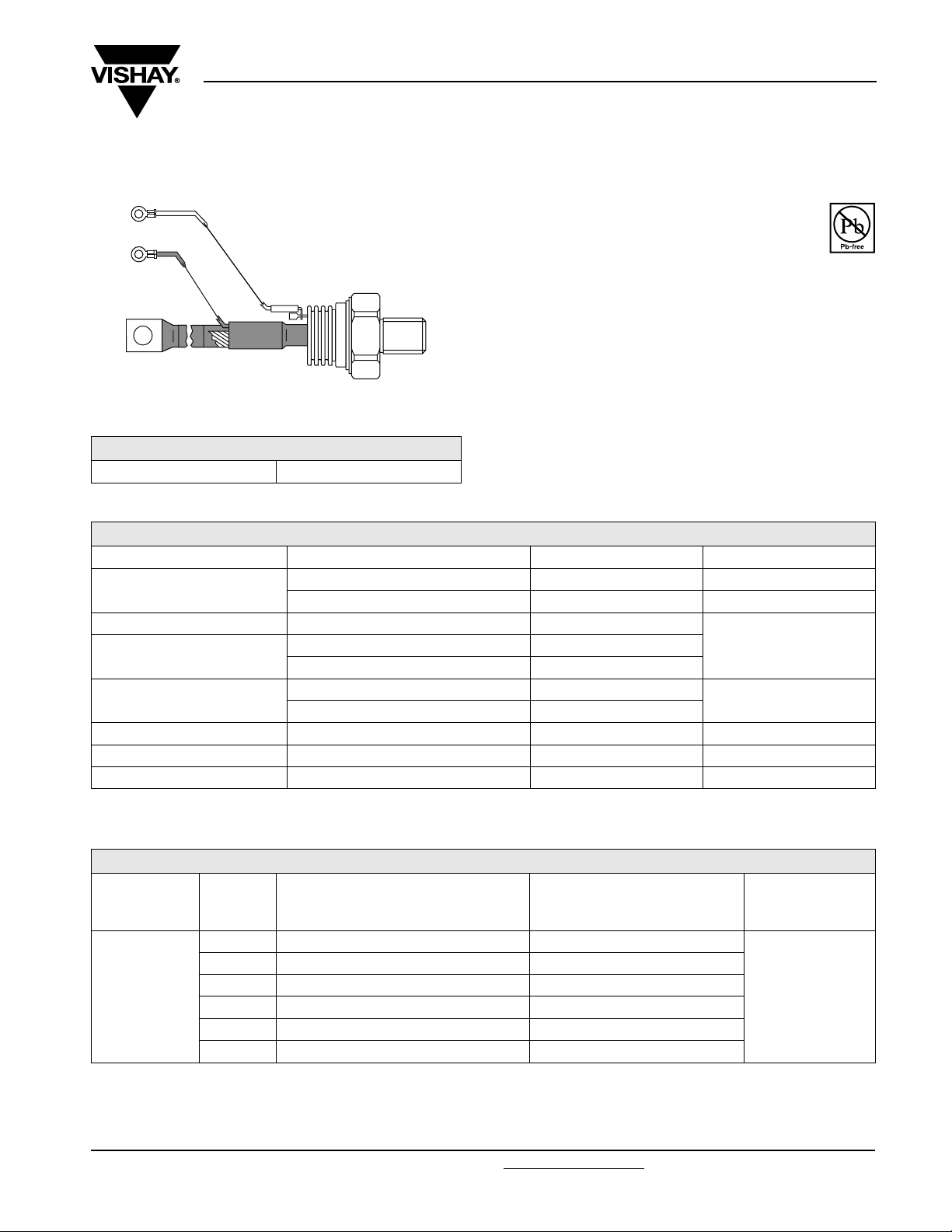
TO-209AE (TO-118)
PRODUCT SUMMARY
I
T(AV)
Vishay High Power Products
Phase Control Thyristors
(Stud Version), 300 A
FEATURES
• Center amplifying gate
• International standard case TO-209AE (TO-118)
• Hermetic metal case with ceramic insulator
• Threaded studs UNF 3/4"-16UNF-2A or ISO M24 x 1.5
• Compression bonded encapsulation for heavy duty
operations such as severe thermal cycling
• Lead (Pb)-free
• Designed and qualified for industrial level
TYPICAL APPLICATIONS
• DC motor controls
300 A
• Controlled DC power supplies
• AC controllers
ST300SPbF Series
RoHS
COMPLIANT
MAJOR RATINGS AND CHARACTERISTICS
PARAMETER TEST CONDITIONS VALUES UNITS
I
T(AV)
I
T(RMS)
I
TSM
2
I
t
V
DRM/VRRM
t
q
T
J
T
C
50 Hz 8000
60 Hz 8380
50 Hz 320
60 Hz 292
Typical 100 µs
300 A
75 °C
470
400 to 2000 V
- 40 to 125 °C
ELECTRICAL SPECIFICATIONS
VOLTAGE RATINGS
TYPE NUMBER
ST300S
V
VOLTAGE
CODE
04 400 500
08 800 900
12 1200 1300
16 1600 1700
18 1800 1900
20 2000 2100
DRM/VRRM
, MAXIMUM REPETITIVE PEAK
AND OFF-STATE VOLTAGE
V
V
, MAXIMUM
NON-REPETITIVE PEAK VOLTAGE
RSM
V
I
DRM/IRRM
AT T
A
kA2s
MAXIMUM
= TJ MAXIMUM
J
mA
50
Document Number: 94406 For technical questions, contact: ind-modules@vishay.com
Revision: 11-Aug-08 1
www.vishay.com
Page 2
ST300SPbF Series
Vishay High Power Products
Phase Control Thyristors
(Stud Version), 300 A
ABSOLUTE MAXIMUM RATINGS
PARAMETER SYMBOL TEST CONDITIONS VALUES UNITS
Maximum average on-state current
at case temperature
Maximum RMS on-state current I
I
T(RMS)
Maximum peak, one-cycle
non-repetitive surge current
2
Maximum I
Maximum I
t for fusing I2t
2
√t for fusing I2√t t = 0.1 to 10 ms, no voltage reapplied 3200 kA2√s
Low level value of threshold voltage V
High level value of threshold voltage V
Low level value of on-state slope resistance r
High level value of on-state slope resistance r
Maximum on-state voltage V
Maximum holding current I
Typical latching current I
T(AV)
I
TSM
T(TO)1
T(TO)2
t1
t2
TM
H
L
180° conduction, half sine wave 300 A
75 °C
DC at 64 °C case temperature 470
t = 10 ms
t = 8.3 ms 8380
t = 10 ms
t = 8.3 ms 7040
t = 10 ms
t = 8.3 ms 292
t = 10 ms
t = 8.3 ms 207
(16.7 % x π x I
(I > π x I
(16.7 % x π x I
(I > π x I
No voltage
reapplied
100 % V
reapplied
No voltage
RRM
Sinusoidal half wave,
initial T
= TJ maximum
J
reapplied
100 % V
RRM
reapplied
< I < π x I
T(AV)
), TJ = TJ maximum 0.98
T(AV)
< I < π x I
T(AV)
), TJ = TJ maximum 0.73
T(AV)
), TJ = TJ maximum 0.97
T(AV)
), TJ = TJ maximum 0.74
T(AV)
8000
6730
320
226
Ipk = 940 A, TJ = TJ maximum, tp = 10 ms sine pulse 1.66 V
TJ = 25 °C, anode supply 12 V resistive load
600
1000
A
kA2s
V
mΩ
mA
SWITCHING
PARAMETER SYMBOL TEST CONDITIONS VALUES UNITS
Maximum non-repetitive rate of rise
of turned-on current
Typical delay time t
Typical turn-off time t
dIdt
d
q
Gate drive 20 V, 20 Ω, t
T
= TJ maximum, anode voltage ≤ 80 % V
J
≤ 1 µs
r
DRM
Gate current 1 A, dIg/dt = 1 A/µs
V
= 0.67 % V
d
, TJ = 25 °C
DRM
ITM = 550 A, TJ = TJ maximum, dI/dt = 40 A/µs,
V
= 50 V, dV/dt = 20 V/µs, gate 0 V 100 Ω, tp = 500 µs
R
1000 A/µs
1.0
µs
100
BLOCKING
PARAMETER SYMBOL TEST CONDITIONS VALUES UNITS
Maximum critical rate of rise of
off-state voltage
Maximum peak reverse and
off-state leakage current
dV/dt T
,
I
RRM
I
DRM
= TJ maximum linear to 80 % rated V
J
TJ = TJ maximum, rated V
DRM/VRRM
DRM
500 V/µs
applied 30 mA
www.vishay.com For technical questions, contact: ind-modules@vishay.com
Document Number: 94406
2 Revision: 11-Aug-08
Page 3
ST300SPbF Series
Phase Control Thyristors
Vishay High Power Products
(Stud Version), 300 A
TRIGGERING
PARAMETER SYMBOL TEST CONDITIONS
Maximum peak gate power P
Maximum average gate power P
Maximum peak positive gate current I
Maximum peak positive gate voltage + V
Maximum peak negative gate voltage - V
G(AV)
GM
TJ = TJ maximum, tp ≤ 5 ms 10.0
GM
TJ = TJ maximum, f = 50 Hz, d% = 50 2.0
TJ = TJ maximum, tp ≤ 5 ms 3.0 A
GM
TJ = TJ maximum, tp ≤ 5 ms
GM
TJ = - 40 °C
DC gate current required to trigger I
DC gate voltage required to trigger V
DC gate current not to trigger I
DC gate voltage not to trigger V
GT
GT
GD
GD
= 25 °C 100 200
J
T
= 125 °C 50 -
J
TJ = - 40 °C 2.5 -
= 25 °C 1.8 3
T
J
= 125 °C 1.1 -
T
J
Maximum required gate trigger/
current/voltage are the lowest
value which will trigger all units
12 V anode to cathode applied
Maximum gate current/voltage
not to trigger is the maximum
TJ = TJ maximum
value which will not trigger any
unit with rated V
anode to
DRM
cathode applied
VALUES
TYP. MAX.
20
5.0
200 -
10 mA
0.25 V
UNITS
W
V
mAT
V
THERMAL AND MECHANICAL SPECIFICATIONS
PARAMETER SYMBOL TEST CONDITIONS VALUES UNITS
Maximum operating junction temperature range T
Maximum storage temperature range T
Maximum thermal resistance, junction to case R
Maximum thermal resistance, case to heatsink R
J
Stg
thJC
thCS
DC operation 0.10
Mounting surface, smooth, flat and greased 0.03
Mounting torque, ± 10 % Non-lubricated threads
Approximate weight 535 g
Case style See dimensions - link at the end of datasheet TO-209AE (TO-118)
ΔR
CONDUCTION
thJC
CONDUCTION ANGLE SINUSOIDAL CONDUCTION RECTANGULAR CONDUCTION TEST CONDITIONS UNITS
180° 0.011 0.008
120° 0.013 0.014
T
90° 0.017 0.018
= TJ maximum K/W
J
60° 0.025 0.026
30° 0.041 0.042
Note
• The table above shows the increment of thermal resistance R
when devices operate at different conduction angles than DC
thJC
- 40 to 125
- 40 to 150
48.5
(425)
(lbf · in)
°C
K/W
N · m
Document Number: 94406 For technical questions, contact: ind-modules@vishay.com
www.vishay.com
Revision: 11-Aug-08 3
Page 4

ST300SPbF Series
Vishay High Power Products
130
120
110
100
90
80
70
Maximum Allowable Case Temperature (°C)
0 50 100 150 200 250 300 350
Fig. 1 - Current Ratings Characteristics Fig. 2 - Current Ratings Characteristics
ST3 00 S Se r ie s
R (DC) = 0.10 K/ W
thJC
Cond uction Ang le
30°
60°
90°
120°
180°
Average On-state Current (A)
480
440
400
360
320
280
180°
120°
90°
60°
30°
RM S Li m i t
240
200
160
120
80
40
0
Maximum Average On-state Power Loss (W)
0 40 80 120 160 200 240 280 320
Avera ge On-state Current (A)
Phase Control Thyristors
(Stud Version), 300 A
130
120
110
100
90
80
70
60
Maximum Allowable Case Temp erature (°C)
0100200300400500
R
0
.
0
t
8
h
S
K
A
/
W
0
.
1
2
K
/
W
0
.
2
K
/
W
0
.
3
K
/
W
0
.
4
K
/
Conduction Angle
ST300S Se rie s
T = 125°C
J
W
0
.
6
K
/
W
1
.
2
K
/
W
25 50 75 100 125
Maximum Allowable Ambient Temperature (°C)
Fig. 3 - On-State Power Loss Characteristics
=
0
.
0
3
K
/
W
D
e
l
t
a
ST3 00 S Se r ie s
R (DC) = 0.10 K/W
thJC
Conduc tion Period
30°
60°
90°
120°
Averag e On-sta te Current (A)
R
180°
DC
650
600
550
500
450
400
350
300
250
200
150
100
50
Maximum Averag e On-state Power Loss (W)
DC
180°
120°
90°
60°
30°
RM S Li m it
0
0
100 200 300 400 500
Average On-state Current (A)
Conduction Period
ST300S Se rie s
T = 125°C
J
R = 0. 03 K/
th
S
A
0
.
0
8
K
0
.
1
2
K
0
.
2
K
0
.
3
K
0
.
6
K
1
.
2
K
W
/
W
De
l
t
/
W
/
W
/
W
/
W
/
W
a
R
25 50 75 100 125
Maximum Allowable Ambient Temperature (°C)
Fig. 4 - On-State Power Loss Characteristics
www.vishay.com For technical questions, contact: ind-modules@vishay.com
Document Number: 94406
4 Revision: 11-Aug-08
Page 5

ST300SPbF Series
Phase Control Thyristors
Vishay High Power Products
(Stud Version), 300 A
7500
At Any Ra te d Loa d Cond ition And With
Rat ed V App lied Following Surg e.
7000
6500
6000
5500
5000
4500
4000
3500
Pe a k Ha lf Sine Wave On-sta te Current (A)
3000
110100
Number Of Equal Amp litud e Half Cycle C urrent Pulses (N)
RRM
ST3 00 S Se r ie s
Ini t ial T = 12 5°C
J
@ 60 Hz 0.0083 s
@ 50 Hz 0.0100 s
Fig. 5 - Maximum Non-Repetitive Surge Current Fig. 6 - Maximum Non-Repetitive Surge Current
10000
T = 2 5° C
J
T = 12 5° C
J
8500
Maximum Non Repetitive Surge Current
Peak Half Sine Wa ve On-stat e Current (A)
8000
7500
7000
6500
6000
5500
5000
4500
4000
3500
3000
Versus Pulse Train Dura tion. Control
Of Cond uc tion May Not Be Maintained .
ST300S Series
0.01 0.1 1
Pulse Tra in Du ra t io n ( s)
Initia l T = 125°C
No Voltage Reapplied
Rated V Reap plied
RRM
J
1000
ST3 00 S Se r i e s
Instantaneous On-state Current (A)
100
0123456789
Instantaneous On-state Voltage (V)
Fig. 7 - On-State Voltage Drop Characteristics
1
Stead y Stat e Value
R = 0. 10 K/ W
thJC
(DC Operation)
thJC
0.1
0.01
ST3 0 0 S Se r i e s
0.001
Tran sient Therma l Imp ed anc e Z (K/ W)
0.001 0.01 0. 1 1 10
Sq u a r e W a v e P u l se D u r a t i o n ( s)
Fig. 8 - Thermal Impedance Z
Characteristics
thJC
Document Number: 94406 For technical questions, contact: ind-modules@vishay.com
www.vishay.com
Revision: 11-Aug-08 5
Page 6

ST300SPbF Series
Vishay High Power Products
100
Rectangular gate pulse
a) Recommended load line for
rated di/dt : 20V, 10ohms; tr<=1 µs
b) Recommended load line for
<=30% rated di/ dt : 10V, 10ohms
10
tr<=1 µs
1
Instantaneous Gate Voltag e (V)
0.1
0.001 0.01 0.1 1 10 100
ORDERING INFORMATION TABLE
Device code
ST 30 0 S 20 P 0 - PbF
VGD
Phase Control Thyristors
(Stud Version), 300 A
(a)
(b)
Tj = - 4 0 °C
Tj = 25 ° C
Tj = 12 5 ° C
IG D
Device : ST300S Series
Fig. 9 - Gate Characteristics
Instantaneous Gate Current (A)
Fre q u e n c y Lim i t ed b y PG ( A V)
(1) PGM = 10W, tp = 4ms
(2) PGM = 20W, tp = 2ms
(3) PGM = 40W, tp = 1ms
(4) PGM = 60W, tp = 0.66ms
(2)
(1)
(3)
(4)
324
51
6789
1 - Thyristor
2 - Essential part number
3 - 0 = Converter grade
4
- S = Compression bonding stud
5
- Voltage code x 100 = V
6
- P = Stud base 3/4" 16UNF-2A threads
(see Voltage Ratings table)
RRM
M = Stud base metric threads (M24 x 1.5)
7
- 0 = Eyelet terminals (gate and auxiliary cathode leads)
1 = Fast-on terminals (gate and auxiliary cathode leads)
3 = Threaded top terminal 3/8" 24UNF-2A
8 - Critical dV/dt:
None = 500 V/µs (standard value)
L = 1000 V/µs (special selection)
9 - Lead (Pb)-free
LINKS TO RELATED DOCUMENTS
Dimensions http://www.vishay.com/doc?95084
www.vishay.com For technical questions, contact: ind-modules@vishay.com
6 Revision: 11-Aug-08
Document Number: 94406
Page 7

Legal Disclaimer Notice
Vishay
Notice
The products described herein were acquired by Vishay Intertechnology, Inc., as part of its acquisition of
International Rectifier’s Power Control Systems (PCS) business, which closed in April 2007. Specifications of the
products displayed herein are pending review by Vishay and are subject to the terms and conditions shown below.
Specifications of the products displayed herein are subject to change without notice. Vishay Intertechnology, Inc., or
anyone on its behalf, assumes no responsibility or liability for any errors or inaccuracies.
Information contained herein is intended to provide a product description only. No license, express or implied, by
estoppel or otherwise, to any intellectual property rights is granted by this document. Except as provided in Vishay's
terms and conditions of sale for such products, Vishay assumes no liability whatsoever, and disclaims any express
or implied warranty, relating to sale and/or use of Vishay products including liability or warranties relating to fitness
for a particular purpose, merchantability, or infringement of any patent, copyright, or other intellectual property right.
The products shown herein are not designed for use in medical, life-saving, or life-sustaining applications.
Customers using or selling these products for use in such applications do so at their own risk and agree to fully
indemnify Vishay for any damages resulting from such improper use or sale.
International Rectifier
are registered trademarks of International Rectifier Corporation in the U.S. and other countries. All other product
names noted herein may be trademarks of their respective owners.
®
, IR®, the IR logo, HEXFET®, HEXSense®, HEXDIP®, DOL®, INTERO®, and POWIRTRAIN
®
Document Number: 99901 www.vishay.com
Revision: 12-Mar-07 1
Page 8

DIMENSIONS in millimeters (inches)
Ceramic housing
22 (0.87) MAX.
TO-209AE (TO-118)
Case Style TO-209AE (TO-118)
4.3 (0.17) DIA.
Outline Dimensions
Vishay High Power Products
4.5 (0.18) MAX.
Red silicon rubber
38 (1.50)
MAX. DIA.
245 (9.65)
255 (10.04)
Red shrink
MAX.
27.5 (1.08)
Ceramic housing
10.5 (0.41)
NOM.
3/4"16 UNF-2A
49 (1.92) MAX.
Case Style TO-209AE (TO-118)
17 (0.67) DIA.
3/8"-24UNF-2A
White gate
Red cathode
White shrink
245 (9.65) ± 10 (0.39)
MAX.
47 (1.85)
SW 45
21 (0.82) MAX.
(1)
with top thread terminal 3/8"
Flexible leads
C.S. 50 mm
(0.078 s.i.)
2
Fast-on terminals
AMP. 280000-1
REF-250
9.5 (0.37) MIN.
22 (0.86) MIN.
25 (0.98)
38 (1.5) DIA. MAX.
77.5 (3.05)
80.5 (3.17)
MAX.
27.5 (1.08)
3/4"-16UNF-2A
SW 45
(1)
MAX.
47 (1.85)
21 (0.83) MAX.
Note
(1)
For metric device: M24 x 1.5 - length screw 21 (0.83) maximum
Document Number: 95084 For technical questions concerning discrete products, contact: diodes-tech@vishay.com
Revision: 02-Aug-07 For technical questions concerning module products, contact: ind-modules@vishay.com
www.vishay.com
1
 Loading...