

Datasheet ST26C32ABTR, ST26C32ABN, ST26C32ABDR, ST26C32ABD Datasheet (SGS Thomson Microelectronics)
Page 1
ST26C32A
CMOS QUAD 3-STATE
DIFFERENTIAL LINERECEIVER
April 2000
■ CMOSDESIGNFORLOW POWER
■ ±
02VSENSIVITYOVERINPUTCOMMON
MODEVOLTAGERANGE
■ TYPICAL PROPAGATIONDALAYS:19ns
■
TYPICAL INPUTHYSTERESIS:60mV
■ INPUTWILLNOT LOADLINEWHENV
CC
=0V
■
MEETSTHEREQUIREMENTSOFEIA
STANDARDRS-422,RS-423
■ 3-STATEOUTPUTSFORCONNECTIONTO
SYSTEMBUSES
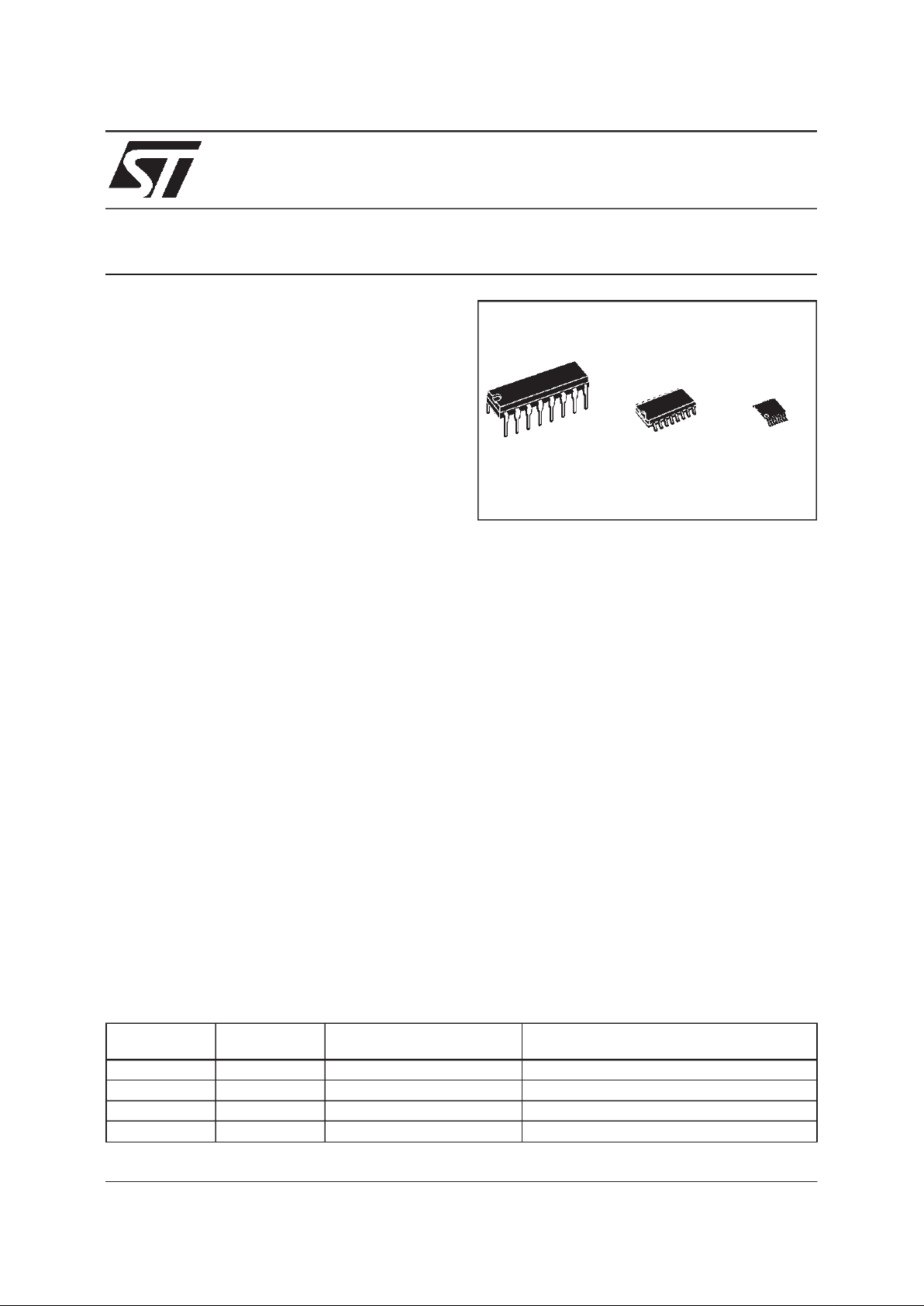
■ AVAILABLEIN SURF AC EMOUNT
DESCRIPTION
The ST26C32A is a quad differential line receiver
designed to meet the RS-422, RS-423 standards
for balanced and unbalanced digital data
trasmission, while retaining the low power
characteristics of CMOS. The ST26C32A has an
input sensivity of 200mV over the common mode
input voltage range of±7V. The ST26C32A
features internal pull-up and pull-down resistors
ORDERCODES
Typ e Temp erature
Range
Packag e Commen ts
ST26C32ABN -40 to 85
o
C DIP-16 25 parts per tube / 40 tube per box
ST26C32ABD -40 to 85
o
C SO-16 (Tube) 50 parts per tube / 20 tube per box
ST26C32ABDR -40 to 85
o
C SO-16 (Tape & Reel) 2500 parts per reel
ST26C32ABTR -40 to 85
o
C TSSOP16 (Tape & Reel) 2500 parts per reel
which prevent output oscillation on unused
channels. The ST26C32A provides an enable
and disable function to all four receivers and
features 3-STATE output with 6mA source and
sinkcapability.
SOPDIP TSSOP
1/8
Page 2
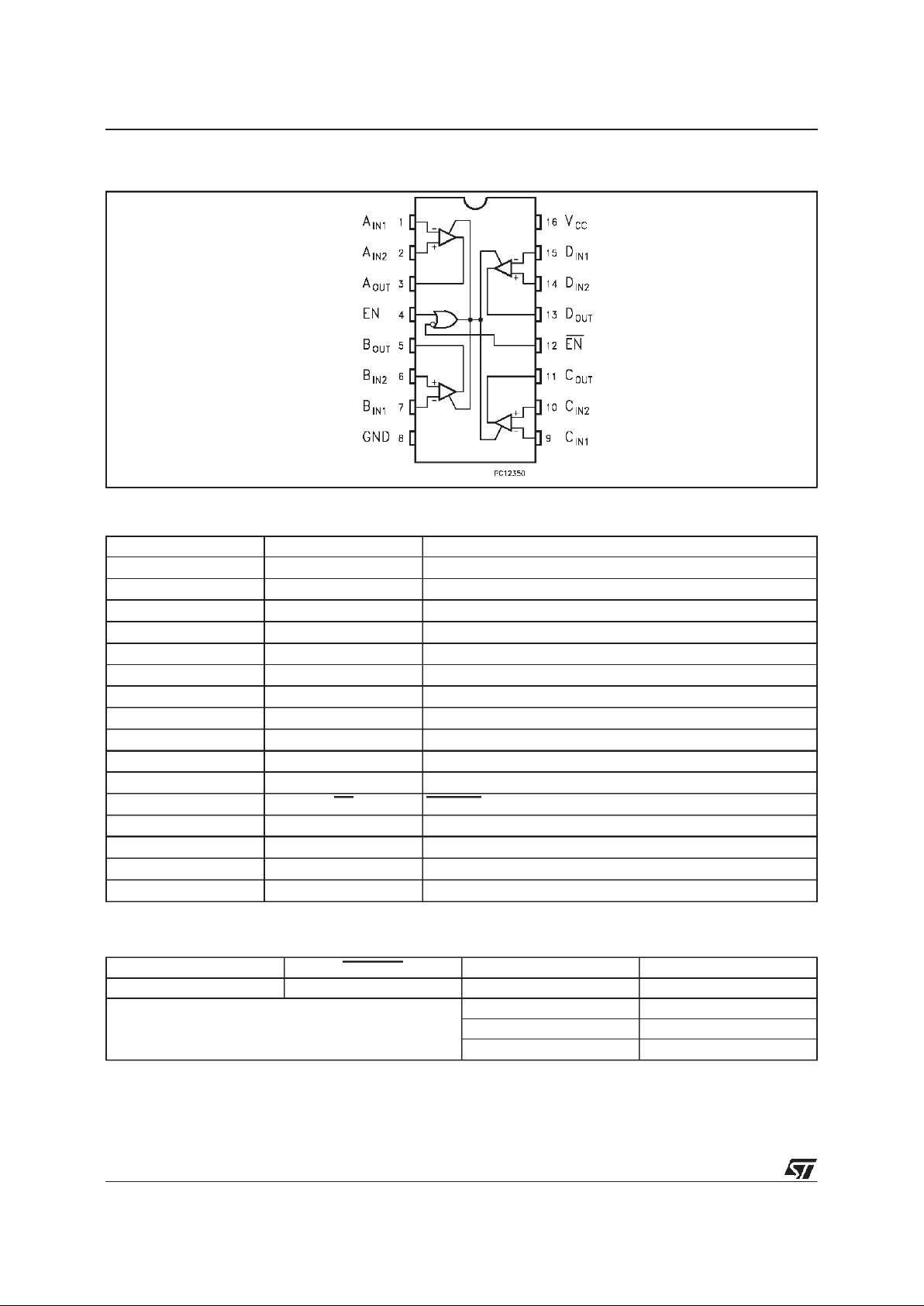
PIN CONFIGURATION
PIN DESCRIPTION
PIN N o SYM BO L NAM E AND FUNC T I O N
1A
IN1
INPUT A1
2A
IN2
INPUT A2
3A
OUT
Channel A Output
4 EN ENABLE
5B
OUT
Channel B Output
6B
IN2
INPUT B2
7B
IN1
INPUT B1
8 GND Ground
9C
IN1
INPUT C1
10 C
IN2
INPUT C2
11 C
OUT
Channel C Output
12 EN ENABLE
13 D
OUT
Channel D Output
14 D
IN2
INPUT D2
15 D
IN1
INPUT D1
16 V
CC
Supply Voltage
TRUTH TABLE
ENABLE E NABLE INPUT OUTPUT
LHXZ
All other combinations of enableinputs V
ID
≥ V
TH(MAX)
H
V
ID
≤
V
TH(MIN)
L
Open H
L=Low Voltage State
H=HighLogicState
X=Don’t Care
Z=High Impedance
ST26C32A
2/8
Page 3
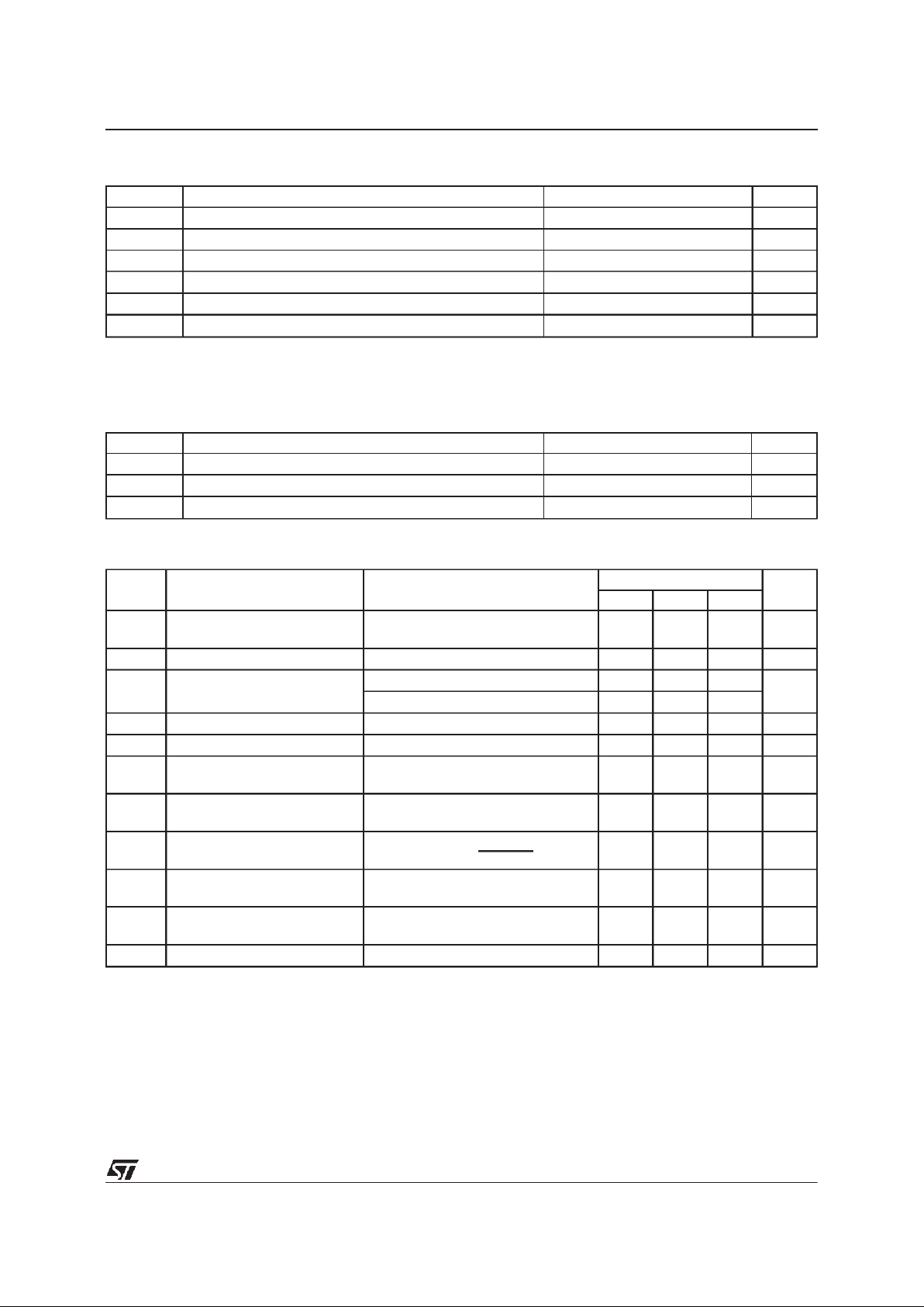
ABSOLUTE MAXIMUM RATINGS
(Note 1, 2)
Symb o l Para met er Val u e Unit
V
CC
Supply Voltage 7 V
V
CM
Input Common Mode Range
±
14 V
V
DIFF
Differential Input Voltage
±
14 V
V
IN
Enable Input Voltage 7 V
I
OMAX
Maximum Current per Output ± 25 mA
T
stg
Storage Temperature Range -65 to +150
o
C
Note1: Absolute Maximum Ratings are those values beyond which thesafety of the device cannot be guaranteed. They are notmeant to imply that the
device should be operated at these limits. Thetableof electrical characteristics provide conditions foractual device operation.
Note2:Unlessotherwisespecified,allvoltagearereferenced toground.
RECOMMENDEDOPERATING CONDITIONS
Symbol Parameter Value Unit
V
CC
Supply Voltage 4.5 to 5.5 V
T
A
Operating Temperature Range -40 to +85
o
C
t
r,tf
Maximum Enable Input Rise or Fall Times 500 ns
ELECTRICALCHARACTERISTICS (VCC=5V±10% unless otherwise specified,See Note 1)
Symbol Parameter Test Conditio ns Value Un it
Min. Typ. Max.
V
TH
Minimum Differential Input
Voltage
V
OUT=VOH
or VOL,-7V<VCM< 7V -200 35 200 mV
R
IN
Input Resistance VIN= -7V, 7V Other Input = GND 5 6.8 10 K
Ω
I
IN
Input Current VIN= 10V Other Input = GND 1.1 1.5 mA
V
IN
= -10V Other Input = GND -2 -2.5
V
OH
High Level Output Voltage V
DIFF
=1V, I
OUT
= -6mA 3.8 4.2 V
V
OL
Low Level Output Voltage V
DIFF
=-1V, I
OUT
= +6mA 0.2 0.3 V
V
IH
Minimum Enable High Input
Level Voltage
2V
V
IL
Maximum Enable Low Input
Level Voltage
0.8 V
I
OZ
3-STATE Output Leakage
Current
V
OUT=VCC
or GND
ENABLE = V
IL
ENABLE= V
IH
±0.5 ±5.0 µA
I
I
Maximum Enable Input
Current
VIN=VCCor GND ±1.0 µA
I
CC
Quiescent Power Supply
Current
VCC=Max, V
(DIFF)
=1V 16 23 mA
V
HYST
Input Hysteresis VCM=0V 60 mV
Note1:Unlessotherwisespecified.min/maxlimitsapplyacrosstherecommended operatingtemperature range.
AlltypicalaregivenforV
CC
=5VandTa=25oC
ST26C32A
3/8
Page 4

SWITCHINGCHARACTERISTICS
(V
CC
=5V±10%,See Note 1)
Symbol Parameter Test Conditio ns Value Un it
Min. Typ. Max.
t
PLH
t
PHL
Propagation Delay Input to
Output
CL= 50pF V
DIFF
=2.5V
V
CM
=0V
19 30 ns
t
RISE
t
FALL
Output Rise and Fall Times CL= 50pF V
DIFF
=2.5V
V
CM
=0V
49ns
t
PZH
t
PZL
Propagation Enable Time to
Output
CL= 50pF V
DIFF
=2.5V
R
L
= 1000
Ω
13 23 ns
t
PHZ
t
PLZ
Propagation Disable Time to
Output
CL= 50pF V
DIFF
=2.5V
R
L
= 1000
Ω
13 22 ns
Note1:Unlessotherwisespecified,min/maxlimitsapplyacrosstherecommended operatingtemperature range.
AlltypicalaregivenforV
CC
=5VandTa=25oC
ST26C32A
4/8
Page 5

DIM.
mm inch
MIN. TYP. MAX. MIN. TYP. MAX.
a1 0.51 0.020
B 0.77 1.65 0.030 0.065
b 0.5 0.020
b1 0.25 0.010
D 20 0.787
E 8.5 0.335
e 2.54 0.100
e3 17.78 0.700
F 7.1 0.280
I 5.1 0.201
L 3.3 0.130
Z 1.27 0.050
P001C
Plastic DIP-16 (0.25) MECHANICAL DATA
ST26C32A
5/8
Page 6

DIM.
mm inch
MIN. TYP. MAX. MIN. TYP. MAX.
A 1.75 0.068
a1 0.1 0.2 0.004 0.007
a2 1.65 0.064
b 0.35 0.46 0.013 0.018
b1 0.19 0.25 0.007 0.010
C 0.5 0.019
c1 45 (typ.)
D 9.8 10 0.385 0.393
E 5.8 6.2 0.228 0.244
e 1.27 0.050
e3 8.89 0.350
F 3.8 4.0 0.149 0.157
G 4.6 5.3 0.181 0.208
L 0.5 1.27 0.019 0.050
M 0.62 0.024
S 8 (max.)
P013H
SO-16 MECHANICAL DATA
ST26C32A
6/8
Page 7

DIM.
mm inch
MIN. TYP. MAX. MIN. TYP. MAX.
A 1.1 0.433
A1 0.05 0.10 0.15 0.002 0.004 0.006
A2 0.85 0.9 0.95 0.335 0.354 0.374
b 0.19 0.30 0.0075 0.0118
c 0.09 0.20 0.0035 0.0079
D 4.9 5 5.1 0.193 0.197 0.201
E 6.25 6.4 6.5 0.246 0.252 0.256
E1 4.3 4.4 4.48 0.169 0.173 0.176
e 0.65 BSC 0.0256 BSC
K0
o
4
o
8
o
0
o
4
o
8
o
L 0.50 0.60 0.70 0.020 0.024 0.028
c
E
b
A2
A
E1
D
1
PIN 1 IDENTIFICATION
A1
L
K
e
TSSOP16 MECHANICAL DATA
ST26C32A
7/8
Page 8

Information furnished isbelieved to be accurate and reliable. However, STMicroelectronics assumes no responsibility for the consequences
of use of such information nor for any infringement of patents or other rights of third parties which may result from its use. No license is
granted by implication or otherwise under any patent or patent rights of STMicroelectronics. Specification mentioned in this publication are
subject tochange without notice. Thispublication supersedes and replaces all informationpreviously supplied. STMicroelectronics products
are not authorized for use as critical components in lifesupport devices or systems withoutexpress written approval of STMicroelectronics.
The ST logo is a registered trademark of STMicroelectronics
2000 STMicroelectronics – Printed in Italy – All RightsReserved
STMicroelectronics GROUP OF COMPANIES
Australia - Brazil-China - Finland - France -Germany - Hong Kong - India - Italy - Japan- Malaysia - Malta - Morocco
Singapore - Spain- Sweden - Switzerland - United Kingdom - U.S.A.
http://www.st.com
.
ST26C32A
8/8
 Loading...