

Page 1
ST25TV02KC ST25TV512C
Datasheet
NFC Type 5 / RFID tag IC with up to 2.5 Kbits of EEPROM, product identification
and protection
Features
Includes ST state-of-the-art patented technology
Contactless interface
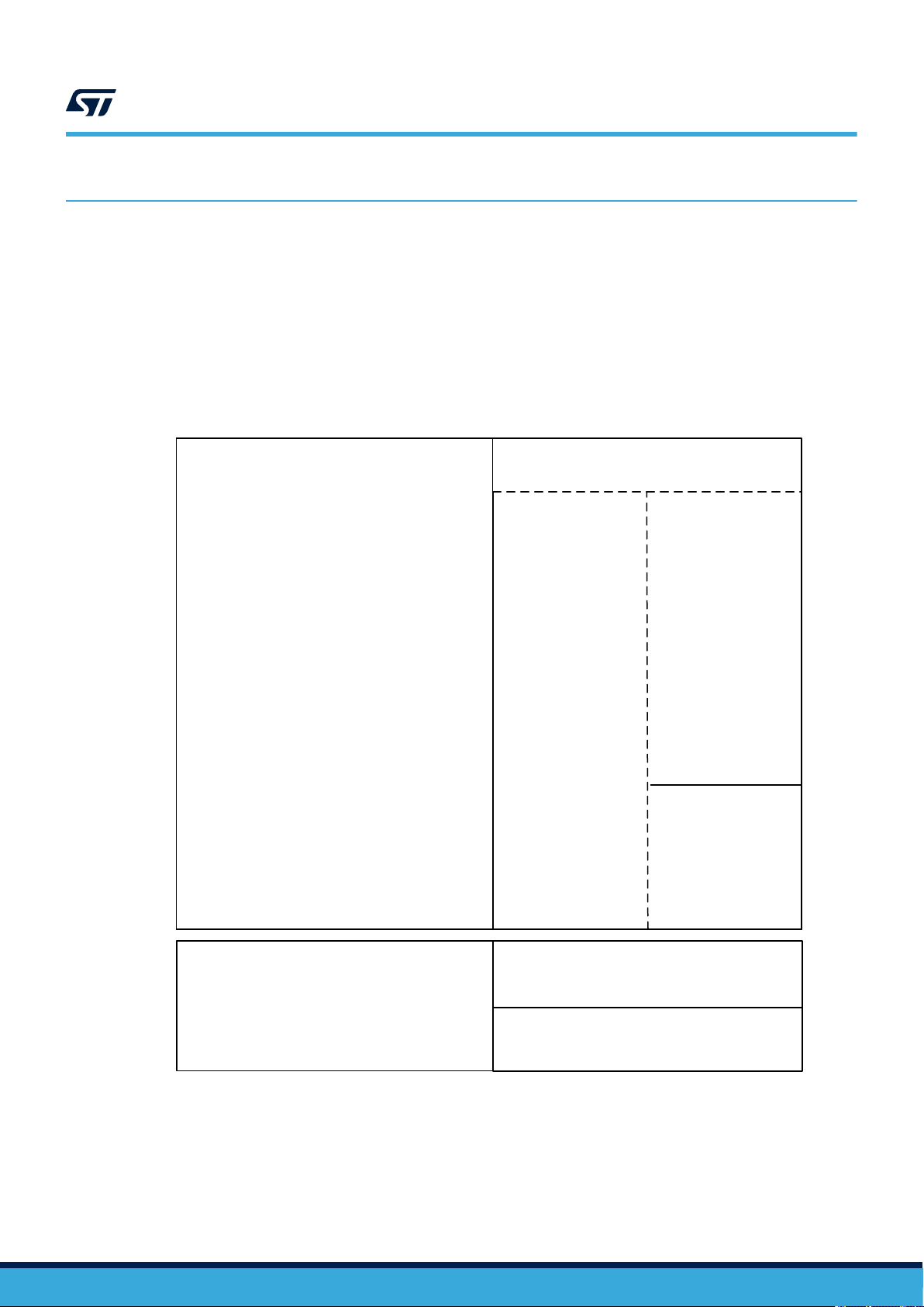
UFDFPN5
1.7 x 1.4 mm
Wafer
Product status link
ST25TV02KC
ST25TV512C
• Compliant with ISO/IEC 15693
• NFC Forum Type 5 tag certified by the NFC Forum
• Supports all ISO/IEC 15693 modulations, coding, subcarrier modes, and
datarates up to 26 Kbit/s
• Single block reads and writes, multiple block reads
• Internal tuning capacitance: 23 pF
Memory
• Up to 2560 bits (320 bytes) of EEPROM
• Accessible by blocks of four bytes
• Write time from RF: typical 5 ms per block
• Data retention: 60 years at 55°C
• Minimum endurance: 100k write cycles
• 3-digit unique tap code
• Augmented NDEF (contextual automatic NDEF message)
Data protection
• User memory configurable in one or two areas:
– in single area mode, access protectable by one 64-bit password
– in flexible dual area mode, access protectable by two 32-bit passwords
• System configuration: access protected by a 32-bit password
• Permanent write lock of specific user area blocks
• Temporary write lock at user area level
• Permanent write lock of specific system configuration blocks
Product identification and protection
• Password features: cover coding, recovery, failed attempt counter
• Tamper detection capability with memorization of open/resealed events
• TruST25 digital signature
Privacy
• Configurable kill mode for permanent deactivation of the tag
• Untraceable mode with configurable responsiveness
Temperature range
• From - 40 to 85 °C
DS13304 - Rev 3 - April 2021
For further information contact your local STMicroelectronics sales office.
www.st.com
Page 2

ST25TV02KC ST25TV512C
Package
• 5-pin package, ECOPACK2 (RoHS compliant)
• Bumped and sawn wafer
DS13304 - Rev 3
page 2/87
Page 3
1 Description
The ST25TV02KC and ST25TV512C devices are NFC/RFID tag ICs with an Augmented NDEF feature, a tamper
detection interface, and specific modes to protect customer privacy.
The Augmented NDEF feature is a contextual automatic NDEF message service, allowing the tag to respond
dynamic content without an explicit update of the EEPROM by the end-user.
The tamper detection interface is available on ST25TV02KC-T devices only. This interface is not available on
ST25TV02KC‑A and ST25TV512C devices.
The ST25TV02KC and ST25TV512C devices hold a digital signature generated by TruST25 (a set of software
and procedures) to prove the origin of the chip in cloning detection, embeds a configurable EEPROM with 60-year
data retention, and can be operated from a 13.56 MHz long range RFID reader or an NFC phone.
The contactless interface is compliant with the ISO/IEC 15693 standard and NFC Forum Type 5 tag specification.
1.1 Block diagram
The ST25TV02KC and ST25TV512C (hereinafter referred to as ST25TVxxxC) devices are depicted in the
following block diagram:
ST25TV02KC ST25TV512C
Description
Figure 1. ST25TVxxxC block diagram
ANALOG FRONT END
EEPROM
RF interface
AC0
23 pF tuning
capacitance
User memory
(2)
DIGITAL CONTROL
UNIT
AC1
ISO/IEC 15693
protocol and control
Memory control
System registers
1. The tamper detection interface is available on ST25TV02KC-T devices only.
2. Respectively 512 and 2560 bits on ST25TV512C and ST25TV02KC devices.
(1)
TD0
TD1
TAMPER DETECTION
1.2 Package connections
ST25TV02KC and ST25TV512C are provided in two delivery forms:
• UFDFPN5 package (ST25TV02KC-T devices only)
• Sawn and bumped wafer (ST25TV512C, ST25TV02KC-A and ST25TV02KC-T devices)
DS13304 - Rev 3
page 3/87
Page 4
ST25TV02KC ST25TV512C
Package connections
Table 1. Signal names
Signal name Function Direction
AC0 Antenna coils In-out
AC1 Antenna coils In-out
TD0 Tamper detection loop In
TD1 Tamper detection loop Out
Figure 2. UFDFPN5 package connections
TD1
5 1
NC
AC1
4
UFDFPN5 pads side
Figure 3. Die connections for sawn and bumped wafer
AC0 NC
ST25TVxxxC-A
AC1 NC
Bumped pads side
TD0
2
NC
3
AC0
AC0 TD0
ST25TV02KC-T
AC1 TD1
Bumped pads side
DS13304 - Rev 3
page 4/87
Page 5

2 Signal descriptions
2.1 Antenna coil (AC0, AC1)
These inputs are used to connect the ST25TVxxxC device to an external coil exclusively. It is advised not to
connect any other DC or AC path to AC0 or AC1.
When correctly tuned, the coil is used to power and access the device using the ISO/IEC 15693 and ISO 18000-3
mode 1 protocols.
2.2 Tamper detection (TD0, TD1)
These inputs are used to connect a wire loop to the ST25TVxxxC device to detect an open or a short between the
TD0 and TD1 pins.
ST25TV02KC ST25TV512C
Signal descriptions
DS13304 - Rev 3
page 5/87
Page 6
3 Power management
The ST25TVxxxC device is powered through its contactless interface.
3.1 Device set
To ensure a proper boot of the RF circuitry, the RF field must be turned ON without any modulation for a
minimum period of time t
all received RF commands (see Figure 4).
RF Field:
BOOT_RF
(see Table 172. RF characteristics). During t
Figure 4. RF power-up sequence
t
BOOT_RF
ST25TV02KC ST25TV512C
Power management
BOOT_RF
, the ST25TVxxxC ignores
RF State:
3.2 Device reset
To ensure a proper reset of the RF circuitry, the RF field must be turned off (100% modulation) for a minimum
t
amount of time (see Table 172. RF characteristics).
RF_OFF
OFF
Boot
No RF access
allowed
ON = RF interface ready
DS13304 - Rev 3
page 6/87
Page 7
4 Memory management
4.1 Memory organization
The ST25TVxxxC memory is organized as follows:
• User memory: it can be configured in one or two different areas, as described in Section 4.2 User memory.
Those areas can be used for user data and NFC Forum Type 5 Capability Container (CC) if required.
• System configuration memory: it is composed of different registers, including the device configuration, the
ISO15693 AFI and DSFID registers. It also contains the UID and different protection registers. Refer to
Section 4.3 System configuration memory for more details
ST25TV02KC ST25TV512C
Memory management
Figure 5. Memory organization
User memory
(3)
CC File
AREA1
(single area)
(1)
AREA1
(dual area)
AREA2
(dual area)
(2)
(2)
DS13304 - Rev 3
System
CFG
configuration
memory
1. NFC Forum T5T CC file is coded on block 00h which is part of AREA1.
2. In dual area mode, the AREA1/AREA2 boundary can be configured with a block granularity.
3. Respectively 16 and 80 blocks of 32 bits for ST25TV512C and ST25TV02KC devices.
SYS
page 7/87
Page 8
4.2 User memory
User memory is addressed as blocks (= pages) of 4 bytes, starting at address 0 and ending at address
END_MEM. Value of END_MEM is 0Fh and 4Fh for ST25TV512C and ST25TV02KC devices respectively. The
ST25TVxxxC user memory can be configured in single area (AREA1) or in dual area mode (AREA1 and AREA2)
depending on the value of the END_A1 register at the start of a RF session (see Table 2. User memory in single
area mode, Table 3. User memory in dual area mode and Table 13. END_A1 content).
When the value of END_A1 is equal to END_MEM, the ST25TVxxxC user memory is configured in single area
mode defined as follows:
• AREA1 starts at address 00h. It is composed of (END_MEM+1) blocks. It can be read- or readwriteprotected by a dedicated 64-bit password. AREA1 is dedicated to user data.
When the value of END_A1 is lower than END_MEM, the ST25TVxxxC user memory is configured in dual area
mode defined as follows :
• AREA1 starts at address 00h. It is composed of (END_A1+1) blocks. It can be read- or readwrite-protected
by a dedicated 32-bit password. AREA1 is dedicated to user data.
• AREA2 starts at address (END_A1+1). It is composed of (END_MEM-END_A1) blocks. It can be read- or
readwrite-protected by a dedicated 32-bit password. AREA2 is dedicated to user data.
Block 00h belongs to AREA1, but can always be read regardless of the read-protection mode of AREA1. This
block is dedicated to the CC file content defined by the NFC Forum Type 5 application. An application that does
not need to comply with NFC Forum Type 5 specifications can use block 00h for any purpose.
ST25TV02KC ST25TV512C
User memory
Table 2. User memory in single area mode
RF command
ReadSingleBlock
ReadMultipleBlocks
WriteSingleBlock
Block
address
(1)
00h
LSByte - - MSByte
0000h 0001h 0002h 0003h
01h 0004h 0005h 0006h 0007h
02h 0008h 0009h 000Ah 000Bh
... ... ... ... ...
END_MEM END_MEM*4+0 END_MEM*4+1 END_MEM*4+2 END_MEM*4+3
1. Block 00h is always readable
2. For single area mode, set the value of END_A1 register to END_MEM
Byte address
Table 3. User memory in dual area mode
RF command
Block
address
(1)
00h
LSByte - - MSByte
0000h 0001h 0002h 0003h
01h 0004h 0005h 0006h 0007h
02h 0008h 0009h 000Ah 000Bh
ReadSingleBlock
ReadMultipleBlocks
WriteSingleBlock
... ... ... ... ...
END_A1 END_A1*4+0 END_A1*4+1 END_A1*4+2 END_A1*4+3
END_A1+1 END_A1*4+4 END_A1*4+5 END_A1*4+6 END_A1*4+7
... ... ... ... ...
END_MEM END_MEM*4+0 END_MEM*4+1 END_MEM*4+2 END_MEM*4+3
1. Block 00h is always readable
2. For dual area mode, set value of END_A1 register between 00h and (END_MEM-1)
Byte address
Comment
(2)
AREA1
Comment
(2)
AREA1
(2)
AREA2
DS13304 - Rev 3
page 8/87
Page 9

4.3 System configuration memory
In addition to user memory, ST25TVxxxC includes a set of registers located in the system configuration memory.
Registers are read during the boot sequence and define basic ST25TVxxxC behaviour.
4.3.1 System configuration registers
Table 4. List of configuration registers lists the configuration registers of the ST25TVxxxC device. They are
accessed with the ReadConfiguration and WriteConfiguration commands and two arguments FID and PID,
respectively acting as a feature identifier and a parameter identifier.
The write access to the configuration registers is protected by the CONFIG security session which is opened by a
successful presentation of the PWD_CFG password (see Section 5.1.2 Password management).
Configuration registers are grouped by FID value. The write access to a group of registers may be permanently
locked.
Depending on the configuration register, its read access is either always granted or protected with the same
mechanisms as its write access.
Depending on the configuration register, when its content is updated during a RF session, the effect of the new
value is activated either immediately or at the start of the next RF session.
Table 4. List of configuration registers
Name
RW_PROTECTION_A1 00h 00h 1 Y W B Section 5.1.1
END_A1 00h 01h 1 Y W' B Section 5.1.1
RW_PROTECTION_A2 01h 00h 1 Y W B Section 5.1.1
UTC_EN 02h 00h 1 Y W B Section 5.2.1
UTC 02h 01h 3 Y N - Section 5.2.1
TD_EVENT_UPDATE_EN
TD_SEAL_MSG
TD_UNSEAL_MSG
TD_RESEAL_MSG
TD_SHORT_MSG
TD_OPEN_MSG
TD_STATUS
(4)
(4)
(4)
(4)
(4)
(4)
ANDEF_EN 04h 00h 1 Y W B Section 5.4.1
ANDEF_CFG 04h 01h 2 Y W B Section 5.4.1
ANDEF_SEP 04h 02h 1 R W I Section 5.4.1
ANDEF_CUSTOM_LSB 04h 03h 4 R W I Section 5.4.1
ANDEF_CUSTOM_MSB 04h 04h 4 R W I Section 5.4.1
PRIVACY 05h 00h 1 Y W B Section 5.5.1
AFI_PROT 08h 00h 1 Y W B Section 5.7.1
REV FEh 00h 1 Y N - Section 5.9
UID FEh 01h 8 Y N - Section 5.9
LCK_CONFIG FFh 00h 2 Y W'' I Section 5.1.1
1. Y: read access not protected, R: read access granted if LCK_CONFIG[FID]=0b and CONFIG security session open
2. N: write access not available, W: write access granted if LCK_CONFIG[FID]=0b and CONFIG security session open, W':
write access granted if LCK_CONFIG[1:0]=00b and CONFIG security session open, W'': write access granted if CONFIG
security session open
3. B: update is effective on next RF boot sequence, I: update is effective immediately
FID PID Bytes
(4)
03h 00h 1 Y W B Section 5.3.1
03h 01h 2 R W I Section 5.3.1
03h 02h 2 R W I Section 5.3.1
03h 03h 2 R W I Section 5.3.1
03h 04h 1 R W I Section 5.3.1
03h 05h 1 R W I Section 5.3.1
03h 06h 3 Y N - Section 5.3.1
Read
ST25TV02KC ST25TV512C
System configuration memory
(1)
Write
(2)
Activation time
(3)
Section
DS13304 - Rev 3
page 9/87
Page 10

4. Registers with FID=03h are available only on ST25TV02KC-T devices (see section 10)
4.3.2 System registers
Table 5 lists the system registers of the ST25TVxxxC device. They are accessed with other RF commands than
ReadConfiguration and WriteConfiguration.
When the write access to a system register is available, it may be protected by a password and/or a lock
mechanism.
When the read access to a system register is available, it is always granted through the relevant RF command.
When the content of a system register is updated, the effect of the new value is activated immediately.
Name Bytes
LCK_BLOCK 10 R W I Section 5.1.1
LCK_DSFID 1 N W I Section 5.9
LCK_AFI 1 N W I Section 5.9
DSFID 1 Y W I Section 5.9
AFI 1 Y W I Section 5.9
IC_REF 1 Y N - Section 5.9
UID 8 Y N - Section 5.9
ANDEF_UID 16 Y N - Section 5.4.1
KILL_CMD 1 N W I Section 5.5.1
UNTR_CMD 1 N W I Section 5.5.1
RND_NUMBER 2 Y
PWD_CFG 4 N W I Section 5.1.1
PWD_A1 4 N W I Section 5.1.1
PWD_A2 4 N W I Section 5.1.1
PWD_UNTR 4 N W I Section 5.1.1
1. Y: read access granted without condition, R: read access granted with condition
2. N: write access not available, W: write access granted with condition
3. The content of the RND_NUMBER register is updated internally on a successful GetRandomNumber request
Table 5. List of system registers
Read
(1)
Write
N
(2)
(3)
Activation time Section
ST25TV02KC ST25TV512C
System configuration memory
- Section 5.1.1
DS13304 - Rev 3
page 10/87
Page 11
5 Specific features
ST25TVxxxC offers the following features:
• Section 5.1 Data protection
• Section 5.2 Unique tap code
• Section 5.3 Tamper detection
• Section 5.4 Augmented NDEF
• Section 5.5 Consumer privacy protection
• Section 5.6 TruST25 digital signature
• Section 5.7 AFI protection
• Section 5.8 Inventory Initiated
The features from Section 5.1 to Section 5.7 can be programmed by accessing registers of the ST25TVxxxC
using the ReadConfiguration and WriteConfiguration commands. Update of configuration registers is only possible
when the access right has been granted by presenting the configuration password (PWD_CFG), and if the
configuration of the feature was not previously locked (see register LCK_CONFIG).
Depending on the configuration register, the effect of a valid write access may be applied immediately or during
the boot sequence of the next RF session.
An additional set of registers allows to identify and customize the product (see Section 5.9 Device identification
registers.).
ST25TV02KC ST25TV512C
Specific features
5.1 Data protection
ST25TVxxxC provides a special data protection mechanism based on passwords that unlock security sessions.
Read and/or write access to the user memory can be protected. Write access to the configuration registers is
always protected. Read access to some configuration registers is protected.
Other lock mechanisms are supported (LockBlock, lock by feature), as described in this section.
5.1.1 Data protection registers
RF Command Access type
ReadConfiguration @(FID=FFh, PID=00h) R : always possible
WriteConfiguration @(FID=FFh, PID=00h)
Table 6. LCK_CONFIG access
W : if the CONFIG security session is open
W effective time : immediate
DS13304 - Rev 3
page 11/87
Page 12
ST25TV02KC ST25TV512C
Data protection
Table 7. LCK_CONFIG content
Bit Name Function Factory value
b0 LCK_A1
b1 LCK_A2
b2 LCK_UTC
b3 LCK_TD
b4 LCK_ANDEF
b5 LCK_PRIV
b7-b6 RFU - 00b
b8 LCK_AFIP
b15-b9 RFU - 0000000b
0: configuration registers with FID=00h are not locked
1: configuration registers with FID=00h are locked
0: configuration registers with FID=01h are not locked
1: configuration registers with FID=01h are locked
0: configuration registers with FID=02h are not locked
1: configuration registers with FID=02h are locked
0: configuration registers with FID=03h are not locked
1: configuration registers with FID=03h are locked
0: configuration registers with FID=04h are not locked
1: configuration registers with FID=04h are locked
0: configuration registers with FID=05h are not locked
1: configuration registers with FID=05h are locked
0: configuration registers with FID=08h are not locked
1: configuration registers with FID=08h are locked
0b
0b
0b
0b
0b
0b
0b
Note: Refer to Table 4. List of configuration registers for the LCK_CONFIG register.
If value 1b is issued for a field already set to 1b, the WriteConfiguration command has no effect and error 11h
shall be responded.
Otherwise, if value 0b is issued for a field set to 1b, the corresponding feature remains locked and no errorcode is
responded to the WriteConfiguration command.
Table 8. LCK_BLOCK access
RF Command
ReadSingleBlock
ReadMultipleBlocks
GetMultipleBlockSecurityStatus
R : if Option_flag=1 and write access to parent area is allowed
R : if Option_flag=1 and write access to parent area is allowed
R : if write access to parent area is allowed
LockBlock W : if not already locked and write access to parent area is allowed
- W effective time : immediate
1. When the write access to an area is not allowed (write access forbidden, or protected with closed security session),
then the value of LCK_BLOCK is masked by 1 in a BSS field (see sections Section 6.4.3 ReadSingleBlock,
Section 6.4.6 ReadMultipleBlocks and Section 6.4.14 GetMultipleBlockSecurityStatus)
Access type
Table 9. LCK_BLOCK content
Bit
b79-b0 LCK_BLOCK
Name Function Factory Value
For each bit bN:
• 0: write access of block N not locked
• 1: write access of block N permanently
(1)
(1)
(1)
0
Note: Refer to Table 5. List of system registers for the LCK_BLOCK register.
DS13304 - Rev 3
page 12/87
Page 13

ST25TV02KC ST25TV512C
Data protection
Table 10. RW_PROTECTION_A1 access
RF Command Type
ReadConfiguration @(FID=00h, PID=00h) R : always possible
WriteConfiguration @(FID=00h, PID=00h)
Table 11. RW_PROTECTION_A1 content
Bit Name Function Factory Value
AREA1 access rights (except block 00h):
• 00: read always allowed / write always allowed
• 01: read always allowed / write allowed if AREA1 security
• 10: read allowed if AREA1 security session is open /
b1-b0 RW_PROTECTION_A1
b7-b2 RFU - 000000b
• 11: read allowed if AREA1 security session is open /
Block 00h access rights: read always allowed
• 00: write always allowed
• 01: write allowed if AREA1 security session is open
• 10: write allowed if AREA1 security session is open
• 11: write forbidden
W : if the CONFIG security session is open and LCK_A1=0b
W effective time : on next RF boot sequence
session is open
write allowed if AREA1 security session is open
write forbidden
00b
Note: Refer to Table 4. List of configuration registers for the RW_PROTECTION_A1 register.
Table 12. END_A1 access
RF command
ReadConfiguration @(FID=00h, PID=01h) R : always possible
WriteConfiguration @(FID=00h, PID=01h)
W : if the CONFIG security session is open and LCK_A1=LCK_A2=0b
W effective time : on next RF boot sequence
Access type
Table 13. END_A1 content
Bit
b7-b0 END_A1
1. END_MEM value is 0Fh / 4Fh for ST25TV512C / ST25TV02KC devices respectively.
Name Function Factory Value
Number of the last block belonging to AREA1.
When lower than END_MEM, user memory is split in two
areas :
• AREA1 (blocks 00h to END_A1)
• AREA2 (blocks END_A1 + 1 to END_MEM).
Otherwise user memory contains a single area : AREA1
(blocks 00h to END_MEM)
Note: Refer to Table 4. List of configuration registers for the END_A1 register.
END_MEM
(1)
DS13304 - Rev 3
page 13/87
Page 14
ST25TV02KC ST25TV512C
Data protection
Table 14. RW_PROTECTION_A2 access
RF command Access type
ReadConfiguration @(FID=01h, PID=00h) R : always possible
WriteConfiguration @(FID=01h, PID=00h)
Table 15. RW_PROTECTION_A2 content
Bit Name Function Factory Value
AREA2 access rights:
• 00: read always allowed / write always allowed
• 01: read always allowed / write allowed if AREA2 security
b1-b0 RW_PROTECTION_A2
b7-b2 RFU - 000000b
session is open
• 10: read allowed if AREA2 security session is open / write
allowed if AREA2 security session is open
• 11: read allowed if AREA2 security session is open / write not
allowed
W : if the CONFIG security session is open and LCK_A2=0b
W effective time : on next RF boot sequence
00b
Note: Refer to Table 4. List of configuration registers for the RW_PROTECTION_A2 register.
Table 16. PWD_CFG access
RF command
- R: no read access
WritePassword @PID=00h
W: if the CONFIG security session is open
W effective time: immediate
Access type
Table 17. PWD_CFG content
Bit Name Function
b31-b0 PWD_CFG Password for access to configuration registers and Kill command 00000000h
Note: Refer to Table 5. List of system registers for the PWD_CFG register.
Factory
Value
DS13304 - Rev 3
page 14/87
Page 15

Table 18. PWD_A1 access
RF command Access type
- R : no read access
WritePassword @PID=01h
W : if AREA1 security session is open
W effective time : immediate
Table 19. PWD_A1 content
Bit Name Function Factory Value
b31-b0 PWD_A1_LSB Password for access to AREA1 00000000h
In single area mode, bits 0 to 63 are used.
(1)
In dual area mode only bits 0 to 31 are used
b63-b32
PWD_A1_MSB
1. PWD_A1_MSB is an alias of register PWD_A2:
• when switching from dual to single area mode, the value of PWD_A1_MSB is the latest known value of PWD_A2
• when switching from single to dual area mode, the value of PWD_A2 is the latest known value of PWD_A1_MSB
Note: Refer to Table 5. List of system registers for the PWD_A1 register.
ST25TV02KC ST25TV512C
Data protection
00000000h
Table 20. PWD_A2 access
RF command
- R : no read access
WritePassword @PID=02h
W : if AREA2 security session is open
W effective time : immediate
Table 21. PWD_A2 content
Bit
b31-b0
1. PWD_A1_MSB is an alias of register PWD_A2:
• when switching from dual to single area mode, the value of PWD_A1_MSB is the latest known value of PWD_A2
• when switching from single to dual area mode, the value of PWD_A2 is the latest known value of PWD_A1_MSB
Name Function Factory Value
PWD_A2
(1)
Password for access to AREA2 00000000h
Note: Refer to Table 5. List of system registers for the PWD_A2 register.
Table 22. PWD_UNTR access
RF command
- R : no read access
WritePassword @PID=03h
W : if UNTR security session is open
W effective time : immediate
Access type
Access type
Table 23. PWD_UNTR content
Bit
b31-b0 PWD_UNTR Password used with ToggleUntraceable command 00000000h
Name Function Factory Value
Note: Refer to Table 5. List of system registers for the PWD_UNTR register.
DS13304 - Rev 3
page 15/87
Page 16

Table 24. RND_NUMBER access
RF command Access type
GetRandomNumber R : always possible
1. the content of the RND_NUMBER register is updated internally on a successful GetRandomNumber command.
-
W : no write access
Table 25. RND_NUMBER content
Bit Name Function Factory value
b15-b0 RND_NUMBER 16-bit random number N/A
Note: Refer to Table 5. List of system registers for the RND_NUMBER register.
5.1.2 Password management
ST25TVxxxC provides protection of user and system configuration memories. Access to groups of data are
controlled by security sessions based on passwords. On successful (respectively failed) presentation of a
password, a security session is open (respectively closed) and grants (respectively denies) access to the
protected group of data.
ST25TV02KC ST25TV512C
Data protection
(1)
Table 26. Security session type
Security session Open by presenting Rights granted when session is open
CONFIG PWD_CFG
AREA1 PWD_A1
AREA2 PWD_A2
UNTR PWD_UNTR Update of PWD_UNTR
Access to configuration registers
Update of PWD_CFG
Access to blocks from AREA1 in user memory
Update of PWD_A1
Access to blocks from AREA2 in user memory
Update of PWD_A2
Each of the PWD_CFG and PWD_UNTR passwords is 32-bit long.
In dual area mode (END_A1 < END_MEM), each of the PWD_A1 and PWD_A2 passwords is 32-bit long.
In single area mode (END_A1 = END_MEM), the PWD_A1 password is 64-bit long, and AREA2 security session
is not applicable: password commands fail with password identifier 02h when single area mode is used.
Note: In addition to the security session mechanism described in this section, the PWD_CFG and PWD_UNTR
passwords are respectively used with the Kill and ToggleUntraceable commands.
Table 27. List of password registers
Password
PWD_CFG 00h 4 bytes
PWD_A1 01h
PWD_A2 02h
PWD_UNTR 03h 4 bytes
Password_id Password_data size
4 bytes if END_A1 < END_MEM
8 bytes if END_A1 = END_MEM
4 bytes if END_A1 < END_MEM
Invalid request if END_A1 = END_MEM
DS13304 - Rev 3
page 16/87
Page 17

ST25TV02KC ST25TV512C
Data protection
The ST25TVxxxC passwords management is based on three commands:
• WritePassword (see Section 6.4.18 WritePassword)
• PresentPassword (see Section 6.4.19 PresentPassword)
• GetRandomNumber (see Section 6.4.24 GetRandomNumber)
For any of the 4x passwords available, three actions are possible:
• Open Security Session:
– Use GetRandomNumber command if needed
– Use PresentPassword command with corresponding password identifier and valid encrypted password
value (see Section 5.1.4 User memory protection)
• Update Password:
– While the security session for the corresponding password is open, use WritePassword command with
same password identifier and the new encrypted password value (see Section 5.1.4 User memory
protection).
• Close Security Session:
– To close the security session corresponding to a password identifier, user can choose one of the
following options:
◦ Remove tag from RF field
◦ Use PresentPassword command with same password identifier and an invalid password value
◦ Open a security session corresponding to a different password identifier. Opening a new security
session automatically closes the previously opened one (even if the open operation fails)
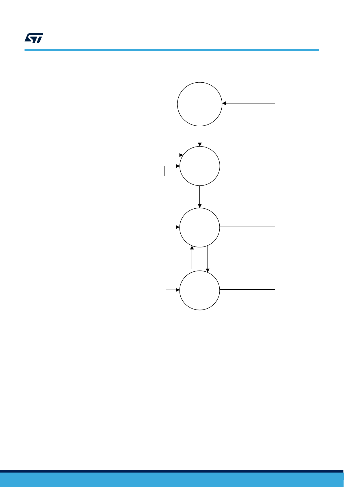
Figure 6 describes the mechanism to open/close the security sessions.
DS13304 - Rev 3
page 17/87
Page 18
ST25TV02KC ST25TV512C
Figure 6. Security sessions management
ST25TVxxxC
out of RF field
Data protection
Present any
password not OK
Any other
command
Any other
command
PWD_x OK
Any other
command
Present
Field ON
All security
sessions
closed
PWD_x OK
Security
session x
opened
(y closed)
Security
session y
opened
(x closed)
Field OFF
Present
Present
PWD_y OK
DS13304 - Rev 3
Password recovery
The ST25TVxxxC devices provide a password recovery feature, which allows the user to reprogram a corrupted
password after a RF field failure during a WritePassword command.
Refer to “AN5577 - Password management for ST25TV512C and ST25TV02KC devices", for more details on how
to use it. Contact your STMicroelectronics sales office to get this document.
Password attempt limit
The ST25TVxxxC devices offer the capability to protect a password against brute-force attacks, thanks to a limiter
mechanism on failed password attempts.
Refer to “AN5577 - Password management for ST25TV512C and ST25TV02KC devices", for more details on how
to use it. Contact your STMicroelectronics sales office to get this document.
page 18/87
Page 19
ST25TV02KC ST25TV512C
Data protection
5.1.3 Password encryption
An encryption mechanism - known as cover coding - is used to transmit coded password values in the
Password_data field of the following command frames:
• PresentPassword request (see Section 6.4.19 PresentPassword),
• WritePassword request (see Section 6.4.18 WritePassword)
• Kill request (see Section 6.4.20 Kill)
• ToggleUntraceable request (see Section 6.4.23 ToggleUntraceable)
The mechanism requires that a call to the GetRandomNumber command has been issued since the latest boot of
the ST25TVxxxC device, otherwise these password commands fail.
Additionally, if the latest call to a PresentPassword / Kill / ToggleUntraceable command failed because of an
invalid value of the Password_data field, it is required that a call to the GetRandomNumber command is issued
before attempting a new call to either of these three commands, otherwise their execution will fail regardless of
the new value of the Password_data field.
Note: If the latest execution of a PresentPassword / ToggleUntraceable command was successful, it is not necessary
to issue a new call to the GetRandomNumber command before issuing a new PresentPassword / Kill /
ToggleUntraceable request.
Assuming these constraints are fulfilled, let the RND_NUMBER_4B and RND_NUMBER_8B values be computed
from the concatenation of the RND_NUMBER register value returned by the latest call to the GetRandomNumber
request.
Table 28. RND_NUMBER_4B
b31-b16
RND_NUMBER RND_NUMBER
b15-b0
Table 29. RND_NUMBER_8B
b63-b48
RND_NUMBER RND_NUMBER RND_NUMBER RND_NUMBER
b47-b32 b31-b16 b15-b0
Let PASSWORD_4B (resp. PASSWORD_8B) be the unencrypted value of a 32-bit (resp. 64-bit) password to be
transmitted over a PresentPassword / WritePassword / Kill / ToggleUntraceable request.
The Password_data field in a request frame shall be computed as follows :
• for a 32-bit password :
Password_data = XOR(RND_NUMBER_4B , PASSWORD_4B)
–
• for a 64-bit password :
Password_data = XOR(RND_NUMBER_8B , PASSWORD_8B)
–
Table 30. Example of 64-bit Password_data value computation
Data name
RND_NUMBER - - - - - - 1Dh E6h
RND_NUMBER_8B 1Dh E6h 1Dh E6h 1Dh E6h 1Dh E6h
PASSWORD_8B FAh D7h 5Eh 15h CAh A5h D0h D4h
Password_data E7h 31h 43h F3h D7h 43h CDh 32h
b63-b56 b55-b48 b47-b40 b39-b32 b31-b24 b23-b16 b15-b8 b7-b0
Note: A field coded on several bytes – such as Password_data – is transmitted in LSB to MSB byte order in ISO15693
request and response frames
DS13304 - Rev 3
page 19/87
Page 20

When processing a PresentPassword / Kill / ToggleUntraceable request, the ST25TVxxxC device decrypts the
Password_data field to obtain the unencrypted value PASSWORD_4B (or PASSWORD_8B), which is used for
comparison with the password register identified by the Password_id field.
When processing a WritePassword request, the ST25TVxxxC device decrypts the Password_data field to obtain
the unencrypted value PASSWORD_4B (or PASSWORD_8B) , which is used for update of the password register
identified by the Password_id field.
5.1.4 User memory protection
A read and/or write access protection can be globally applied to the blocks of an area. Such protection can be
individually configured for AREA1 and AREA2, thanks to the RW_PROTECTION_A1 and RW_PROTECTION_A2
registers (see Table 11. RW_PROTECTION_A1 content and Table 15. RW_PROTECTION_A2 content).
On factory delivery, access to AREA1 and AREA2 are not protected. When updating RW_PROTECTION_Ax
registers, the new protection mode is effective during the boot sequence of the next RF session.
In addition to the area protection mechanism, the write access to each block composing AREA1 and AREA2 can
be individually locked thanks to the LockBlock command.
Block 00h is an exception to the area protection mechanism:
• when block 00h is not locked, the protection of its write access is determined by the value of
RW_PROTECTION_A1 register, like other blocks of AREA1
• read access to block 00h is always allowed, regardless of the value of RW_PROTECTION_A1 register
The RW_PROTECTION_A1 register is locked when register LCK_A1 is set to 1b.
The RW_PROTECTION_A2 register is locked when register LCK_A2 is set to 1b.
The END_A1 register is locked when either of LCK_A1 and LCK_A2 registers is set to 1b.
ST25TV02KC ST25TV512C
Data protection
Retrieve the security status of a user memory block
User can read a block security status (BSS) by issuing following commands:
• GetMultipleBlockSecurityStatus
• ReadSingleBlock with Option_flag set to 1
• ReadMultipleBlocks with Option_flag set to 1
For each block, ST25TVxxxC will respond with a BSS byte containing a Lock_bit flag (b0 in Table 31) as specified
in ISO 15693 standard.
Table 31. Block security status
b7
b6 b5 b4 b3 b2 b1 b0
0: RFU
0: Write access to current block granted
1: Write access to current block denied
This Lock_bit flag is set to one if write access to the corresponding block is not allowed. This happens when either
of the following conditions is met:
• the write access to the block was permanently locked (corresponding bit of LCK_BLOCK register set to 1b)
by a successful LockBlock command
• write access to parent area is protected (RW_PROTECTION_Ax = 01b or 10b at start of the RF session)
and security session is closed
• write access to parent area is forbidden (RW_PROTECTION_Ax = 11b at start of the RF session)
5.1.5 System configuration memory protection
Configurations registers listed Table 4. List of configuration registers are accessed using the ReadConfiguration
and WriteConfiguration commands.
Configuration registers are grouped by feature. A group is identified by parameter FID, a register from this group
is identified by parameter PID.
Write access to configuration registers is protected or forbidden.
Note: Write access to read-only configuration registers is forbidden
DS13304 - Rev 3
page 20/87
Page 21
ST25TV02KC ST25TV512C
Unique tap code
Protected write access to a configuration register is granted when the CONFIG security session is open, and its
parent group is not permanently locked.
Read access to configuration registers is protected or always allowed. Protected read access to a configuration
register is granted when the CONFIG security session is open, and its parent group is not permanently locked.
On factory delivery, configuration groups are not locked (all bits of LCK_CONFIG register are set to 0b). A
configuration group identified by FID (00h, 01h, 02h, 03h, 04h, 05h or 08h) can be permanently locked by setting
bit FID of LCK_CONFIG register to 1b:
• if the read access to a configuration register from this group was protected, the register can no longer be
read even if CONFIG security session is open
• if the write access to a configuration register from this group was protected, the register can no longer be
written even if CONFIG security session is open
• write access to LCK_CONFIG register (FID=FFh, PID=00h) is granted when the CONFIG security session is
open
• user cannot unlock a configuration group by setting bit FID of LCK_CONFIG back to 0b, even after opening
CONFIG security session (Lock is permanent)
• user may lock several configuration groups with a single WriteConfiguration command by setting the
respective bits of LCK_CONFIG to 1b in the request
System registers listed in Table 5. List of system registers include passwords, device identification registers, lock
status and command status.
Read access to system registers is available except for passwords, AFI and DSFID lock status , Kill and
ToggleUntraceable command status.
Device identification registers are detailed in section 5.10:
• Write access to AFI and DFSID registers can be respectively locked by LockAFI and LockDSFID
commands. Lock is permanent: once locked, write access to AFI and DSFID registers is forbidden.
• Other device identification registers (IC_REF, UID) are read only registers.
5.2
Unique tap code
5.2.1 Unique tap code registers
Table 32. UTC_EN access
RF command Access type
ReadConfiguration @(FID=02h, PID=00h) R : always possible
WriteConfiguration @(FID=02h, PID=00h)
Bit Name Function Factory value
b0 UTC_EN
b7-b1 RFU - 0000000b
0: Unique tap code is disabled
1: Unique tap code is enabled
Note: Refer to Table 4. List of configuration registers for the UTC_EN register.
W : if the CONFIG security session is open and LCK_UTC=0b
W effective time : on next RF boot sequence
Table 33. UTC_EN content
0b
DS13304 - Rev 3
page 21/87
Page 22
Table 34. UTC access
RF command Access type
ReadConfiguration @(FID=02h, PID=01h) R : always possible
1. the content of the UTC register is updated internally during the RF boot sequence when UTC_EN is set to 1b
-
W : no write access
Table 35. UTC content
Bit Name Function Factory value
b23-b0 UTC Unique tap code value Not applicable
Note: Refer to Table 4. List of configuration registers for the UTC register.
5.2.2 Unique tap code description
When the UTC_EN register is set to 1b, the content of the UTC register is updated internally with a fresh value
during each RF boot sequence. The content of the UTC register is coded in ASCII format.
The UTC_EN register is locked when register LCK_UTC is set to 1b.
Note: When the Unique tap code is enabled, the duration of the RF boot sequence t
• compliant with the 5ms guard-time value defined in the NFC Forum [DIGITAL] specification
• not compliant with the 1ms guard-time value defined in the ISO15693 specification
Refer to “AN5578 - Unique tap code for ST25TV512C and ST25TV02KC devices", for more details on the content
of the UTC register. Contact your STMicroelectronics sales office to get this document.
ST25TV02KC ST25TV512C
Tamper detection
(1)
(see section 8.2) is:
Boot_RF
5.3 Tamper detection
The tamper detection feature is available on ST25TV02KC-T devices only (see section 10). On ST25TVxxxC-A
devices, ReadConfiguration and WriteConfiguration commands requested with FID=03h fail with error code 10h.
5.3.1 Tamper detection registers
Table 36. TD_EVENT_UPDATE_EN access
RF command Access type
ReadConfiguration @(FID=03h, PID=00h) R : always possible
WriteConfiguration @(FID=03h, PID=00h)
Table 37. TD_EVENT_UPDATE_EN content
Bit Name Function Factory value
b0 TD_EVENT_UPDATE_EN
b7- b1 RFU - 0000000b
Note: Refer to Table 4. List of configuration registers for the TD_EVENT_UPDATE_EN register.
W : if the CONFIG security session is open and LCK_TD=0b
W effective time : on next RF boot sequence
0: memorization of tamper events disabled
1: memorization of tamper events enabled
0b
DS13304 - Rev 3
page 22/87
Page 23

ST25TV02KC ST25TV512C
Tamper detection
Table 38. TD_SEAL_MSG access
RF command Access type
ReadConfiguration @(FID=03h, PID=01h) R : if the CONFIG security session is open and LCK_TD=0b
WriteConfiguration @(FID=03h, PID=01h)
Table 39. TD_SEAL_MSG content
Bit Name Function Factory value
b15-b0 TD_SEAL_MSG Value of TD_EVENT displayed before first occurence of a TD_UNSEAL event 3030h
Note: Refer to Table 4. List of configuration registers for the TD_SEAL_MSG register.
Table 40. TD_UNSEAL_MSG access
RF command Access type
ReadConfiguration @(FID=03h, PID=02h) R : if the CONFIG security session is open and LCK_TD=0b
WriteConfiguration @(FID=03h, PID=02h)
W : if the CONFIG security session is open and LCK_TD=0b
W effective time : immediate
W : if the CONFIG security session is open and LCK_TD=0b
W effective time : immediate
Table 41. TD_UNSEAL_MSG content
Bit
b15-b0 TD_UNSEAL_MSG Value of TD_EVENT displayed after first occurrence of a TD_UNSEAL event 5555h
Name Function Factory value
Note: Note: Refer to Table 4. List of configuration registers for the TD_UNSEAL_MSG register.
Table 42. TD_RESEAL_MSG access
RF command
ReadConfiguration @(FID=03h, PID=03h) R : if the CONFIG security session is open and LCK_TD=0b
WriteConfiguration @(FID=03h, PID=03h)
W : if the CONFIG security session is open and LCK_TD=0b
W effective time : immediate
Access type
Table 43. TD_RESEAL_MSG content
Bit
b15-b0 TD_RESEAL_MSG Value of TD_EVENT displayed after occurrence of a TD_RESEAL event 5252h
Name Function Factory value
Note: Note: Refer to Table 4. List of configuration registers for the TD_RESEAL_MSG register.
Table 44. TD_SHORT_MSG access
DS13304 - Rev 3
RF command
ReadConfiguration @(FID=03h, PID=04h) R : if the CONFIG security session is open and LCK_TD=0b
WriteConfiguration @(FID=03h, PID=04h)
W : if the CONFIG security session is open and LCK_TD=0b
W effective time : immediate
Access type
page 23/87
Page 24

ST25TV02KC ST25TV512C
Table 45. TD_SHORT_MSG content
Bit Name Function Factory value
b7- b0 TD_SHORT_MSG
Note: Note: Refer to Table 4. List of configuration registers for the TD_SHORT_MSG register.
RF command Access type
ReadConfiguration @(FID=03h, PID=05h) R : if the CONFIG security session is open and LCK_TD=0b
WriteConfiguration @(FID=03h, PID=05h)
Bit Name Function Factory value
b7- b0 TD_OPEN_MSG
Message displayed when the tamper loop was in closed status during the latest
boot sequence
Table 46. TD_OPEN_MSG access
W : if the CONFIG security session is open and LCK_TD=0b
W effective time : immediate
Table 47. TD_OPEN_MSG content
Message displayed when the tamper loop was in open status during the latest boot
sequence
Tamper detection
63h
6Fh
Note: Refer to Table 4. List of configuration registers for the TD_OPEN_MSG register.
Table 48. TD_STATUS access
RF command
ReadConfiguration @(FID=03h, PID=06h) R : always possible
- W : no write access
Table 49. TD_STATUS content
Bit
b15-b0 TD_EVENT
b23-b16 TD_LOOP
Name Function Factory value
TD_SEAL_MSG, TD_UNSEAL_MSG or TD_RESEAL_MSG
according to result of tamper event detection
TD_SHORT_MSG or TD_OPEN_MSG
according to the status of the tamper loop during the latest boot sequence
Note: Refer to Table 5. List of system registers for the TD_STATUS register.
5.3.2 Tamper detection description
The tamper detection feature allows to check the shortage status between the TD0 and TD1 pins of the
ST25TV02KC-T, and monitor tamper events.
See Section 8.2 RF electrical parameters for recommended impedance values Ropen and Rclosed in cases of
open and closed tamper loop.
The shortage status TD_LOOP and event status TD_EVENT are read in the response to a ReadConfiguration
request with FID=03h and PID=06h.
This is the customer responsibility to check the values of TD_LOOP and TD_EVENT and behave accordingly.
Access type
Not applicable
Not applicable
DS13304 - Rev 3
page 24/87
Page 25

ST25TV02KC ST25TV512C
Augmented NDEF
TD_LOOP
The shortage status TD_LOOP is captured by ST25TV02KC-T each time that the device is powered- up. Value of
TD_LOOP is equal to value of:
• TD_SHORT_MSG when TD0 and TD1 were connected at capture time
• TD_OPEN_MSG when TD0 and TD1 were not connected at capture time
This information will be lost during power off (no permanent storage of TD_LOOP).
TD_EVENT
The TD_EVENT status is used to monitor the first occurrences of TD_UNSEAL and TD_RESEAL events defined
as follows:
• TD_UNSEAL: TD_EVENT_UPDATE_EN register was set to 1b, and TD0 and TD1 were not connected at
capture time
• TD_RESEAL: TD_EVENT_UPDATE_EN register was set to 1b, TD_UNSEAL already occurred, and TD0
and TD1 were connected at capture time
On factory delivery, TD_EVENT_UPDATE_EN is set to 0b and TD_EVENT is set to the value of TD_SEAL_MSG.
When the first TD_UNSEAL event occurs, TD_EVENT is updated to the value of TD_UNSEAL_MSG.
When the first TD_RESEAL event occurs, TD_EVENT is updated to the value of TD_RESEAL_MSG.
The update of the TD_EVENT register occurs during the RF boot sequence, and its value is stored in the
EEPROM of the ST25TV02KC-T device.
When the LCK_TD register is set to 1b, the TD_EVENT_UPDATE_EN, TD_SEAL_MSG, TD_UNSEAL_MSG,
TD_RESEAL_MSG, TD_SHORT_MSG and TD_OPEN_MSG registers are locked.
Note: When TD_EVENT is updated, the duration of the RF boot sequence t
parameters) is:
• compliant with the 5ms guard-time value defined in the NFC Forum [DIGITAL] specification
• not compliant with the 1ms guard-time value defined in the ISO15693 specification
Note: When TD_EVENT_UPDATE_EN and UTC_EN registers are set to 0b, no programmation of the EEPROM
occurs during the RF boot sequence, and its duration is compliant with the 1ms guard-time value defined in the
ISO15693 specification.
Note: Tamper detection events occurring outside of the capture window (for instance while the IC is in POWER-OFF
state, or during the RF session following the boot sequence) are not detected by the ST25TV02KC-T.
(see Section 8.2 RF electrical
Boot_RF
5.4
Augmented NDEF
5.4.1 Augmented NDEF registers
RF command Access type
ReadConfiguration @(FID=04h, PID=00h) R : always possible
WriteConfiguration @(FID=04h, PID=00h)
DS13304 - Rev 3
Table 50. ANDEF_EN access
W : if the CONFIG security session is open and LCK_ANDEF=0b
W effective time : on next RF boot sequence
page 25/87
Page 26
Table 51. ANDEF_EN content
Bit Name Function Factory value
b0 ANDEF_EN
0: ANDEF feature is disabled,
1: ANDEF feature is enabled
b7- b1 RFU - 0000000b
Note: Refer to Table 4. List of configuration registers for the ANDEF_EN register.
Table 52. ANDEF_CFG access
RF command Access type
ReadConfiguration @(FID=04h, PID=01h) R : always possible
WriteConfiguration @(FID=04h, PID=01h)
W : if the CONFIG security session is open and LCK_ANDEF=0b
W effective time : on next RF boot sequence
Table 53. ANDEF_CFG content
ST25TV02KC ST25TV512C
Augmented NDEF
0b
Bit Name Function Factory value
b0 ANDEF_UID_EN
b1 ANDEF_CUS_EN
b2 ANDEF_UTC_EN
0: UID field disabled in ANDEF feature
1: UID field enabled in ANDEF feature
0: Custom field disabled in ANDEF feature
1: Custom field enabled in ANDEF feature
0: Unique tap code field disabled in ANDEF feature
1: Unique tap code field enabled in ANDEF feature
b3 RFU - 0b
0: Tamper detection field disabled in ANDEF feature
b4
ANDEF_TD_EN
b5 ANDEF_SEP_EN
(1)
1: Tamper detection field enabled in ANDEF feature
0: ANDEF field separator disabled
1: ANDEF field separator enabled
b7- b6 ANDEF_BYTE Byte offset in block ANDEF_BLOCK where the ANDEF feature starts operating 00b
b15-b8 ANDEF_BLOCK Block address where the ANDEF feature starts operating 00h
1. relevant on ST25TV02KC-T devices only, forced to 0b on ST25TVxxxC-A devices
Note: Refer to Table 4. List of configuration registers for the ANDEF_CFG register.
Table 54. ANDEF_SEP access
0b
0b
0b
0b
1b
DS13304 - Rev 3
RF command
Access type
ReadConfiguration @(FID=04h, PID=02h) R : if the CONFIG security session is open and LCK_ANDEF=0b
WriteConfiguration @(FID=04h, PID=02h)
W : if the CONFIG security session is open and LCK_ANDEF=0b
W effective time : immediate
Table 55. ANDEF_SEP content
Bit
b7- b0 ANDEF_SEP Character used as ANDEF field separator when ANDEF_SEP_EN=1b 78h
Name Function Factory value
page 26/87
Page 27
ST25TV02KC ST25TV512C
Note: Refer to Table 4. List of configuration registers for the ANDEF_SEP register.
Table 56. ANDEF_CUSTOM_LSB access
RF command Access type
ReadConfiguration @(FID=04h, PID=03h) R : if the CONFIG security session is open and LCK_ANDEF=0b
WriteConfiguration @(FID=04h, PID=03h)
Table 57. ANDEF_CUSTOM_LSB content
Bit Name Function Factory value
b31-b0 ANDEF_CUSTOM_LSB First 4 characters of the ANDEF custom field 2E2E2E2Eh
Note: Refer to Table 4. List of configuration registers for the ANDEF_CUSTOM_LSB register.
Table 58. ANDEF_CUSTOM_MSB access
W : if the CONFIG security session is open and LCK_ANDEF=0b
W effective time : immediate
Augmented NDEF
RF command Access type
ReadConfiguration @(FID=04h, PID=04h) R : if the CONFIG security session is open and LCK_ANDEF=0b
WriteConfiguration @(FID=04h, PID=04h)
W : if the CONFIG security session is open and LCK_ANDEF=0b
W effective time : immediate
Table 59. ANDEF_CUSTOM_MSB content
Bit
b31-b0 ANDEF_CUSTOM_MSB Last 4 characters of the ANDEF custom field 2E2E2E2Eh
Name Function Factory value
Note: Refer to Table 4. List of configuration registers for the ANDEF_CUSTOM_MSB register.
Table 60. ANDEF_UID access
RF command
ReadSingleBlock
ReadMultipleBlocks
- W : no write access
R : if ANDEF_EN=1b and ANDEF_UID_EN=1b
Access type
Table 61. ANDEF_UID content
Bit
b127-b0 ANDEF_UID Value displayed in the UID field of the ANDEF feature UID in ASCII format starting with "E0"
Name Function Factory value
Note: Refer to Table 5. List of system registers for the ANDEF_UID register.
DS13304 - Rev 3
page 27/87
Page 28

ST25TV02KC ST25TV512C
Augmented NDEF
5.4.2 Augmented NDEF description
The Augmented NDEF feature (ANDEF) is a contextual automatic NDEF message service, allowing the tag to
respond dynamic content without an explicit update of the EEPROM by the end user.
The feature is enabled (resp. disabled) when the value of register ANDEF_EN is 1b (resp. 0b) during the
latest RF boot sequence. When the feature is enabled, user memory data at byte addresses ranging from
ANDEF_START to ANDEF_END is replaced by the content of a virtual memory ANDEF_MEM in the response to
ReadSingleBlock and ReadMultipleBlocks requests.
Note: The BSS values responded to ReadSingleBlock and ReadMultipleBlocks requests are not modified when the
ANDEF feature is enabled
Note: The ANDEF feature has no effect on the WriteSingleBlock command. When the feature is enabled, and a
WriteSingleBlock command is issued on a block crossing the [ANDEF_START:ANDEF_END] range, the data
from the command is directly written to user memory, without replacement by volatile memory content.
Table 62. Block data read when ANDEF feature is disabled on ST25TV02KC
Block address
Block data
Byte0 Byte1 Byte2 Byte3
00h
UM000 UM001 UM002 UM003
... ... ... ... ... No bytes read from ANDEF_MEM memory
(3)
4Fh
UM316 UM317 UM318 UM319
1. Block data responded to ReadSingleBlock and ReadMultipleBlocks requests.
2. UM stands for user memory.
3. ST25TV02KC memory size is used in this example. Note that last block address is 0Fh on ST25TV512C devices.
(1)
Comment
First block of UM
Last block of UM
(2)
(2)
Table 63. Block data read when ANDEF feature is enabled on ST25TV02KC
Block address
Block data
Byte0 Byte1 Byte2 Byte3
00h
UM000 UM001 UM002 UM003
... ... ... ... ... -
2Dh UM180 UM181 UM182 UM183
2Eh UM184 AM000 AM001 AM002
2Fh AM003 AM004 AM005 UM191
30h UM192 UM193 UM194 UM195
... ... ... ... ... -
(4)
4Fh
UM316 UM317 UM318 UM319
1. Block data responded to ReadSingleBlock and ReadMultipleBlocks requests.
2. UM stands for user memory
3. AM stands for ANDEF_MEM memory
4. ST25TV02KC memory size is used in this example. Note that last block address is 0Fh on ST25TV512C devices.
(1)
Comment
First block of UM
(2)
Example with
ANDEF_START=185 and
ANDEF_END=190
(6 bytes of UM
Last block of UM
(2)
replaced with AM
(2)
(3)
)
Byte addresses ANDEF_START and ANDEF_END depend on the value of register ANDEF_CFG during the latest
RF boot sequence:
ANDEF_START = ANDEF_BLOCK * 4 + ANDEF_BYTE
•
• ANDEF_END = min(END_MEM * 4 + 3, ANDEF_START + ANDEF_LEN - 1)
DS13304 - Rev 3
Where ANDEF_LEN is the number of bytes available from ANDEF_MEM memory:
• ANDEF_LEN = ANDEF_UID_EN * 16 + ANDEF_CUS_EN * 8 + ANDEF_UTC_EN * 3 + ANDEF_TD_EN * 3
+ ANDEF_SEP_EN*(ANDEF_UID_EN + ANDEF_CUS_EN + ANDEF_UTC_EN + ANDEF_TD_EN - 1)
page 28/87
Page 29

ST25TV02KC ST25TV512C
Augmented NDEF
Content of ANDEF_MEM depends on the values of ANDEF_CFG, ANDEF_UID, ANDEF_CUSTOM_LSB,
ANDEF_CUSTOM_MSB, UTC, TD_STATUS and ANDEF_SEP registers.
The content of ANDEF_MEM is the result of the concatenation of ANDEF fields. Each field corresponds to a
configuration register. The order of appearance, content and condition of presence of each field is listed in the
table below.
Table 64. ANDEF fields concatenated in ANDEF_MEM
Order
1 ANDEF_UID 16 ANDEF_UID_EN=1b
2 ANDEF_SEP 1 ANDEF_UID_EN=1b and ANDEF_CUS_EN=1b and ANDEF_SEP_EN=1b
3 ANDEF_CUSTOM_LSB 4 ANDEF_CUS_EN=1b
4 ANDEF_CUSTOM_MSB 4 ANDEF_CUS_EN=1b
5 ANDEF_SEP 1
6 UTC 3 ANDEF_UTC_EN=1b
7 ANDEF_SEP 1
8 TD_STATUS 3
1. When a register value is coded on several bytes, it is copied in LSB to MSB byte order in the ANDEF_MEM memory.
2. TD_STATUS field available on ST25TV02KC-T devices only
Content
(1)
Bytes Condition of presence
(ANDEF_UID_EN=1b or ANDEF_CUS_EN=1b)
and ANDEF_UTC_EN=1b and ANDEF_SEP_EN=1b
(ANDEF_UID_EN=1b or ANDEF_CUS_EN=1b or ANDEF_UTC_EN=1b)
and ANDEF_TD_EN=1b
ANDEF_TD_EN=1b
(2)
and ANDEF_SEP_EN=1b
(2)
As an example, Figure 7 shows the usage of the ANDEF feature to display the value of the ANDEF_UID and
TD_STATUS registers in a NDEF URI message : the content of the NDEF message may change after a tamper
detection event without modification of the user memory content.
Figure 7. Example of augmented NDEF message on ST25TV02KC-T
DS13304 - Rev 3
On factory delivery, ANDEF_EN register is set to 0b and ANDEF_CFG register is set to 0020h.
page 29/87
Page 30

When the LCK_ANDEF register is set to 1b, ANDEF_EN, ANDEF_CFG, ANDEF_SEP, ANDEF_ CUSTOM_LSB
and ANDEF_CUSTOM_MSB registers are locked.
5.5 Consumer privacy protection
The Kill and Untraceable features offer consumer privacy capabilities required by the GDPR.
5.5.1 Privacy registers
RF command Access type
- R : no read access
Kill
W : if Kill command responds with Error_flag=0b
W effective time : immediate
ST25TV02KC ST25TV512C
Consumer privacy protection
Table 65. KILL_CMD access
Table 66. KILL_CMD content
Bit Name Function Factory value
b0 KILL_CMD
0: successful Kill command did not occur
1: successful Kill command did occur
Note: Refer to Table 5. List of system registers for the KILL_CMD register.
Table 67. UNTR_CMD access
RF command Access type
- R : no read access
ToggleUntraceable
W : if ToggleUntraceable command responds with Error_flag=0b
W effective time : immediate
Table 68. UNTR_CMD content
Bit
b0 UNTR_CMD
Name Function Factory value
0: last successful ToggleUntraceable command occured with Address_flag=0b
1: last successful ToggleUntraceable command occured with Address_flag=1b
Note: Refer to Table 5. List of system registers for the UNTR_CMD register.
0b
0b
DS13304 - Rev 3
Table 69. PRIVACY access
RF command
ReadConfiguration @(FID=05h, PID=00h) R : always possible
WriteConfiguration @(FID=05h, PID=00h)
W : if the CONFIG security session is open and LCK_PRIV=0b
W effective time : on next RF boot sequence
Access type
page 30/87
Page 31

Table 70. PRIVACY content
ST25TV02KC ST25TV512C
Consumer privacy protection
Bit Name Function
00: device boots in UNTRACEABLE state when UNTR_CMD=1b
01: device always boots in UNTRACEABLE state
b1- b0 UNTR_DFT
b2 DIS_INV
b3 DIS_KILL
b7- b4 RFU - 0000b
10: device boots in UNTRACEABLE state when UNTR_CMD=1b or tamper loop is
closed
11: device boots in UNTRACEABLE state when UNTR_CMD=1b or tamper loop is open
0: Inventory command responds in UNTRACEABLE state
1: Inventory command is mute in UNTRACEABLE state
0: Kill command is enabled
1: Kill command is disabled
Note: Refer to Table 4. List of configuration registers for the PRIVACY register.
5.5.2 Kill feature description
When the ST25TVxxxC is in KILLED state, all incoming RF requests are ignored.
The ST25TVxxxC enters the KILLED state on a successful Kill command (see Section 6.4.20 Kill), which sets
the KILL_CMD register to 1b. Once the ST25TVxxxC has entered the KILLED state, it can only switch between
the POWER-OFF and KILLED states (see Section 6.2.8 ISO15693 states).
The Kill command is enabled/disabled when the DIS_KILL register respectively has value 0/1b during the latest
boot sequence. The update of the DIS_KILL register is effective on the next RF boot sequence.
While the Kill command is disabled, the Kill request is ignored and the ST25TVxxxC can not enter the KILLED
state.
On factory delivery, the KILL_CMD and DIS_KILL registers are set to 0b.
When the LCK_PRIV register is set to 1b, the DIS_KILL register is locked.
Factory
value
00b
0b
0b
5.5.3 Untraceable feature description
When the ST25TVxxxC is in UNTRACEABLE state, all incoming RF requests are ignored except:
• GetRandomNumber and ToggleUntraceable requests (see Section 6.4.23 ToggleUntraceable and
Section 6.4.24 GetRandomNumber)
• Inventory and ReadSingleBlock (block 00h only) requests if value of DIS_INV register was 0b during the
latest RF boot sequence
The ST25TVxxxC enters the UNTRACEABLE state on a successful ToggleUntraceable command requested with
Address_flag=1b, which sets the UNTR_CMD register to 1b.
The ST25TVxxxC leaves the UNTRACEABLE state on a successful ToggleUntraceable command requested with
Address_flag=0b, which sets the UNTR_CMD register to 0b.
After a RF boot sequence, the ST25TVxxxC enters the UNTRACEABLE state if KILL_CMD register is set to 0b
and either of the following conditions is met:
• value of UNTR_CMD register is 1b
• value of UNTR_DFT register is 01b
• value of UNTR_DFT register is 10b and tamper loop is closed (ST25TV02KC-T devices only)
• value of UNTR_DFT register is 11b and tamper loop is open (ST25TV02KC-T devices only)
See Section 6.2.8 ISO15693 states for further details.
Note: After a RF boot sequence with KILL_CMD=UNTR_CMD=0b and UNTR_DFT=10b :
• the ST25TV02KC-T enters the UNTRACEABLE state if the tamper loop is closed
• the ST25TV02KC-T enters the READY state if the tamper loop is open
DS13304 - Rev 3
page 31/87
Page 32

ST25TV02KC ST25TV512C
TruST25 digital signature
Note: After a RF boot sequence with KILL_CMD=UNTR_CMD=0b and UNTR_DFT=11b:
• the ST25TV02KC-T enters the UNTRACEABLE state if the tamper loop is open
• the ST25TV02KC-T enters the READY state if the tamper loop is closed
Note: On ST25TVxxxC-A devices, 10b and 11b values of UNTR_DFT register are interpreted as value 00b.
Untraceability of the customer is claimed for the following reasons :
• in a NFC Forum application, block 00h contains the CC file which does not allow to identify a customer
• user blocks 01h to END_MEM - which contain customer data - can not be accessed in UNTRACEABLE
state
• while in UNTRACEABLE state, the UID value used in request and response frames of Inventory and
ReadSingleBlock commands is fixed (see Section 7.1 Untraceable UID) and does not allow to identify a
customer
Furthermore, the user may configure the ST25TVxxxC to ignore Inventory and ReadSingleBlock requests in
UNTRACEABLE state, by setting the DIS_INV register to 1b.
The update of the DIS_INV and UNTR_DFT registers is effective on the next RF boot sequence. On factory
delivery, the DIS_INV and UNTR_DFT registers are set to 0.
When the LCK_PRIV register is set to 1b, the UNTR_DFT and DIS_INV registers are locked.
5.6 TruST25 digital signature
The ST25TVxxxC devices support the TruST25 digital signature feature, which allows the user to verify the
authenticity of the device, thanks to a unique digital signature.
TruST25 solution encompasses secure industrialization processes and tools deployed by STMicroelectronics to
generate, store and check the signature in the device.
Refer to “AN5580 - TruST25 digital signature for ST25TV512C and ST25TV02KC devices", for more details on
how to use it. Contact your STMicroelectronics sales office to get this document.
5.7
AFI protection
5.7.1 AFI protection registers
Table 71. AFI_PROT access
RF command Access type
ReadConfiguration @(FID=08h, PID=00h) R : always possible
WriteConfiguration @(FID=08h, PID=00h)
Bit Name Function Factory value
b0 AFI_PROT
b7- b1 RFU - 0000000b
0: WriteAFI and LockAFI commands do not depend from AREA1 security session
1: WriteAFI and LockAFI commands fail when AREA1 security session is closed
Note: Refer to Table 4. List of configuration registers for the AFI_PROT register.
W : if the CONFIG security session is open and LCK_AFIP=0b
W effective time : on next RF boot sequence
Table 72. AFI_PROT content
0b
DS13304 - Rev 3
page 32/87
Page 33

5.7.2 AFI protection description
This feature allows to protect the WriteAFI and LockAFI commands with the AREA1 security session, and is
configured by register AFI_PROT.
On factory delivery, the AFI_PROT register is set to 0b. When AFI_PROT register is set to 0b:
• the WriteAFI command is successful if the LCK_AFI register is set to 0b, and fails otherwise
• the LockAFI command is successful if the LCK_AFI register is set to 0b, and fails otherwise
When AFI_PROT register is set to 1b:
• the WriteAFI command is successful if AREA1 security session is open and the LCK_AFI register is set to
0b, and fails otherwise
• the LockAFI command is successful if AREA1 security session is open and the LCK_AFI register is set to
0b, and fails otherwise
When the LCK_AFIP register is set to 1b, the AFI_PROT register is locked.
5.8 Inventory Initiated
ST25TVxxxC provides a special feature to improve the anticollision sequence on moving tags using the
Initiate_flag volatile register. This register, controlled by the Initiate command (refer to Section 6.4.21 Initiate),
allows ST25TVxxxC to respond to InventoryInitiated requests (refer to Section 6.4.22 InventoryInitiated).
For applications where multiple tags are crossing the RF field of a reader, it is possible to miss tags when the
standard Inventory command is used. The reason is that the anticollision sequence performs a global tree search,
calling the command at each node and leaf of the tree. In a worst case, a tag WC waits a long delay before it is
inventoried as a leaf of the search. Such delay can be furthermore increased by tags entering the RF field of the
reader during the search, and tag WC may have left the field before being inventoried.
This usecase can be improved by replacing the standard Inventory command with the custom InventoryInitiated
command in the anticollision sequence. When multiple tags are crossing the RF field of the reader, the
anticollision sequence is started by an Initiate command which initiates the set of tags within range.
InventoryInitiated requests are ignored by tags entering the RF field after the Initiate command, they are only
processed by the set of initiated tags, hence bounding the time necessary to complete the anticollision sequence.
When an initiated tag is inventoried, it is sent to QUIET state to ignore further InventoryInitiated requests.
Once an anticollision sequence is completed, the reader starts a new sequence that will operate only on tags
which have entered the RF field during the previous sequence, and so on.
ST25TV02KC ST25TV512C
Inventory Initiated
5.9 Device identification registers
Registers described in this section are located in System configuration memory. Refer to section 4.3 for more
details.
Table 73. LCK_DSFID access
RF command Access type
- R : no read access
LockDSFID
Bit Name Function Factory value
b0 LCK_DSFID
0: successful LockDSFID command did not occur
1: successful LockDSFID command did occur
Note: Refer to Table 5. List of system registers for the LCK_DSFID register.
W : if LCK_DSFID=0b
W effective time : immediate
Table 74. LCK_DSFID content
0b
DS13304 - Rev 3
page 33/87
Page 34

Table 75. LCK_AFI access
RF command Access type
- R : no read access
LockAFI
W : if LCK_AFI=0b and (AFI_PROT=0b or AREA1 security session is open)
W effective time : immediate
Table 76. LCK_AFI content
Bit Name Function Factory value
b0 LCK_AFI
0: successful LockAFI command did not occur
1: successful LockAFI command did occur
Note: Refer to Table 5. List of system registers for the LCK_AFI register.
Table 77. DSFID access
RF command Access type
Inventory R : always possible
GetSystemInfo R : always possible
ExtendedGetSystemInfo R : always possible
Initiate R : always possible
InventoryInitiated R : always possible
WriteDSFID
W : if LCK_DSFID=0b
W effective time : immediate
ST25TV02KC ST25TV512C
Device identification registers
0b
Table 78. DSFID content
Bit
b7-b0 DSFID ISO/IEC 15693 Data Storage Format IDentifier 00h
Name Function Factory value
Note: Refer to Table 5. List of system registers for the DSFID register.
Table 79. AFI access
RF command
GetSystemInfo R : always possible
ExtendedGetSystemInfo R : always possible
WriteAFI
W : if LCK_AFI=0b and (AFI_PROT=0b or AREA1 security session is open)
W effective time : immediate
Table 80. AFI content
Bit
b7-b0 AFI ISO/IEC 15693 Application Family Identifier 00h
Name Function Factory value
Note: Refer to Table 5. List of system registers for the AFI register.
Access type
DS13304 - Rev 3
page 34/87
Page 35

Table 81. IC_REF access
RF command Access type
GetSystemInfo R : always possible
ExtendedGetSystemInfo R : always possible
- W : no access
Table 82. IC_REF content
Bit Name Function Factory value
b7-b0 IC_REF ISO/IEC 15693 IC reference 08h
Note: Refer to Table 5. List of system registers for the IC_REF register.
Table 83. REV access
RF command Access type
ReadConfiguration @(FID=FEh, PID=00h) R : always possible
- W : no access
ST25TV02KC ST25TV512C
Device identification registers
Table 84. REV content
Bit
b7-b0 REV IC revision number 00h
Name Function Factory value
Note: Refer to Table 4. List of configuration registers for the REV register.
Table 85. UID access
RF command
Inventory R : always possible
GetSystemInfo R : always possible
ExtendedGetSystemInfo R : always possible
Initiate R : always possible
InventoryInitiated R : always possible
ReadConfiguration @(FID=FEh, PID=01h) R : always possible
- W : no access
Access type
DS13304 - Rev 3
page 35/87
Page 36

Table 86. UID content
Bit Name Function Factory value
b7-b0
b15-b8 ISO/IEC 15693 UID byte 1
b23-b16 ISO/IEC 15693 UID byte 2
b31-b24 ISO/IEC 15693 UID byte 3
b39-b32 ISO/IEC 15693 UID byte 4
b47-b40 ISO/IEC 15693 UID byte 5 08h
b55-b48 ISO/IEC 15693 UID byte 6 02h
b63-b56 ISO/IEC 15693 UID byte 7 E0h
UID
ISO/IEC 15693 UID byte 0
Note: Refer to Table 5. List of system registers for the UID register.
ST25TV02KC ST25TV512C
Device identification registers
IC manufacturer serial number
DS13304 - Rev 3
page 36/87
Page 37

6 RF Operation
The device follows ISO/IEC 15693 and NFC Forum Type 5 Tag specification for radio- frequency power and
signal interface and for anticollision and transmission protocol.
The device communicates via the 13.56 MHz carrier electromagnetic wave on which incoming data are
demodulated from the received signal amplitude modulation (ASK: amplitude shift keying). The received ASK
wave is 10% or 100% modulated with a data rate of 1.6 Kbit/s using the 1/256 pulse coding mode or a data rate of
26 Kbit/s using the 1/4 pulse coding mode.
Outgoing data are generated by the ST25TVxxxC load variation using Manchester coding with one or two
subcarrier frequencies at 423 kHz and 484 kHz. Data are transferred from the ST25TVxxxC at 6.6 Kbit/s in low
data rate mode and 26 Kbit/s in high data rate mode.
6.1 RF communication
6.1.1 Access to a ISO/IEC 15693 device
The dialog between the reader and the ST25TVxxxC takes place as follows:
• activation of the ST25TVxxxC by the operating field of the reader
• transmission of a command by the reader (ST25TVxxxC detects carrier amplitude modulation)
• transmission of a response by the ST25TVxxxC using load modulation.
These operations use the power transfer and communication signal interface described below. This technique is
called RTF (reader talk first).
ST25TV02KC ST25TV512C
RF Operation
Operating field
The ST25TVxxxC operates continuously between the minimum and maximum values of the electromagnetic field
H defined in Table 172. RF characteristics. The reader has to generate a field within these limits.
Power transfer
Power is transferred to the ST25TVxxxC by radio frequency at 13.56 MHz via coupling antennas in the
ST25TVxxxC and the reader. The operating field of the reader is transformed on the ST25TVxxxC antenna to
an AC voltage that is rectified, filtered and internally regulated. During communications, the amplitude modulation
(ASK) on this received signal is demodulated by the ASK demodulator.
Frequency
The ISO 15693 standard defines the carrier frequency (fC) of the operating field as 13.56 MHz ± 7 kHz.
Note: In this document, fC symbol is used for the nominal value of fCC (fC=13.56 MHz).
6.2
RF protocol
6.2.1 Protocol description
The transmission protocol (or simply “the protocol”) defines the mechanism used to exchange instructions and
data between the VCD (vicinity coupling device) and the VICC (vicinity integrated circuit card) in both directions. It
is based on the concept of “VCD talks first”. The device acts as the VICC.
This means that a ST25TVxxxC does not start transmitting unless it has received and properly decoded an
instruction sent by the VCD. The protocol is based on an exchange of commands, which consist in request/
response transactions between the VCD and the ST25TVxxxC:
• a request is sent from the VCD to the ST25TVxxxC
• a response to this request is sent from the ST25TVxxxC to the VCD.
Each request and each response are contained in a frame. The frames are delimited by a Start of Frame (SOF)
and End of Frame (EOF).
DS13304 - Rev 3
page 37/87
Page 38

ST25TV02KC ST25TV512C
RF protocol
The protocol is bit-oriented. The number of bits transmitted in a frame is a multiple of eight (8), that is an integer
number of bytes.
A single-byte field is transmitted least significant bit (LSBit) first. A multiple-byte field is transmitted least
significant byte (LSByte) first and each byte is transmitted least significant bit (LSBit) first.
Figure 8. ISO15693 protocol timing
VCD
ST25TVxxxC
Timing
6.2.2 Request format
A request frame consists in :
• a SOF
• request flags
• a command code
• request parameters and data
• a CRC
• an EOF.
Request
frame
Request
frame
Response
frame
t
1
t
2
Table 87. General request format
Response
frame
t
1
t
2
SOF Request_flags Opcode Parameters Data CRC_B EOF
- 8 bits 8 bits optional optional 16 bits -
6.2.3 Request flags
In a request frame, the Request_flags field specifies the actions to be performed by the ST25TVxxxC and
whether corresponding fields are present or not.
The Request_flags field consists of eight bits indexed from 0 to 7.
Note: Indexing of bits starts from 0 to comply with the convention used in this specification, however note that indexing
of these bits starts at 1 in the ISO/IEC 15693 specification.
Bit 2 (Inventory_flag) of Request_flags defines the contents of the four MSBs (bits 4 to 7).
When Inventory_flag value is 0, bits 4 to 7 define the ST25TVxxxC selection criteria.
When Inventory_flag value is 1, bits 4 to 7 define the ST25TVxxxC Inventory parameters.
DS13304 - Rev 3
page 38/87
Page 39

ST25TV02KC ST25TV512C
RF protocol
Table 88. Definition of Request_flags LSBs
Bit Flag Decription
0
1
Subcarrier_flag
Datarate_flag
(1)
(1)
2 Inventory_flag
3 Protocol_extension_flag
1. Subcarrier_flag and Datarate_flag refer to the VICC-to-VCD communication.
Table 89. Definition of Request_flags MSBs when Inventory_flag value is 0
Bit Flag Decription
0 : The command is processed according to the value of Address_flag
4
Select_flag
5
Address_flag
6 Option_flag
7 RFU_flag
1. Select_flag=1 and Address_flag=1 is an invalid case, a request with such setting is ignored by the ST25TVxxxC device.
2. The SELECTED state is defined in section 6.2.8
(1)
1 : UID field not present. The command is processed only by the VICC in SELECTED state
0 : UID field not present. command is processed by any VICC
(1)
1 : UID field present. command is processed only by the VICC whose UID matches the field value
0 : Option not activated
1 : Option activated
0 : Unless otherwise specified
1 : Not supported (RFU)
0 : A single subcarrier is used by the VICC
1 : Two subcarriers are used by the VICC
0 : Low data rate is used by the VICC
1 : High data rate used by the VICC
0 : Bits 4 to 7 are described by Table 89
1 : Bits 4 to 7 are described by Table 90
0 : No protocol format extension
1 : Not supported (RFU)
(2)
Table 90. Definition of Request_flags MSBs when Inventory_flag value is 1
Bit
4 AFI_flag
5 Nb_slots_flag
6 Option_flag
7 RFU_flag
6.2.4 Response format
A response frame consists in:
• a SOF
• response flags
• response data
• a CRC
• an EOF
Flag Decription
0 : AFI field is not present
1 : AFI field is present
0 : 16 slots mode
1 : 1 slot mode
0 : Option not activated
1 : Option activated
0 : Unless otherwise specified
1 : Not supported (RFU)
DS13304 - Rev 3
page 39/87
Page 40

ST25TV02KC ST25TV512C
RF protocol
Table 91. General response format
SOF Response_flags Response_data CRC_B EOF
- 8 bits optional 16 bits -
6.2.5 Response flags
In a response frame, the Response_flags field indicates how actions have been performed by the ST25TVxxxC
and whether corresponding fields are present or not.
The Response_flags field consists of eight bits indexed from 0 to 7.
Note: Indexing of bits starts from 0 to comply with the convention used in this specification, however note that indexing
of these bits starts at 1 in the ISO/IEC 15693 specification.
Table 92. Definition of Response_flags
Bit Flag Description
0 Error_flag
1
2
3
4
5
6
7
RFU
0 : No error
1 : Error detected. Error code present in the Data field
0 : Unless otherwise specified
1 : Not supported (RFU)
6.2.6 Response and error codes
If the Error_flag field is set to 1 by the ST25TVxxxC in the response, an Error code field is present and provides
information about the error that occurred.
If an error occurs while processing a command, the ST25TxxxC remains silent instead of responding a frame with
Error_flag set to 1 when :
• Inventory_flag is set to 1
• Inventory_flag, Select_flag and Address_flag are set to 0
Error codes not specified in Table 93 are reserved for future use.
Table 93. General response format when Error_flag equals 1
SOF Response_flags Error_code CRC_B EOF
- 01h 8 bits 16 bits -
Error code Description
01h Invalid IC Mfg code value
02h Invalid request format
03h Invalid Request_flags value
0Fh Error with no information given
10h Requested data not available
Table 94. Definition of response error codes
DS13304 - Rev 3
page 40/87
Page 41

Error code Description
6.2.7 Modes
The term “mode” refers to the mechanism used in a command to specify the set of VICC devices that must
process a request with Inventory_flag set to 0. Three modes are defined depending on the values of Address_flag
and Select_flag defined in Section 6.2.3 Request flags.
Addressed mode
When Address_flag is set to 1 (Addressed mode), the request contains the UID (unique ID) of the addressed
VICC.
Any ST25TVxxxC receiving a request with the Address_flag set to 1 compares the received UID to its own. If
they match the device processes the request (if possible) and returns a response to the VCD as specified in the
command description. Otherwise the device remains silent.
ST25TV02KC ST25TV512C
RF protocol
11h Requested data is already locked and thus cannot be locked again
12h Requested data is locked and its content cannot be changed
13h Programmation of requested data failed
14h Lock of requested data failed
15h Requested data is protected in read
Select mode
When Select_flag is set to 1 (Select mode), the request frame does not contain a UID field. Only the VICC in
SELECTED state that receives a request with Select_flag set to 1 processes it and returns a response to the VCD
as specified in the command description.
The SELECTED state is defined in section 6.2.8. The system design ensures that only one ST25TVxxxC can be
in the SELECTED state at a given time.
Non-Addressed mode (broadcast request)
When Address_flag and Select_flag are set to 0 (Non-Addressed mode), the request frame does not contain a
UID field.
Several VICC may answer to a request in Non-Addressed mode, unlike the Addressed and Select modes where
at most one VICC is expected to answer.
6.2.8 ISO15693 states
• POWER-OFF
• READY
• QUIET
• SELECTED
Transitions between these states are specified in Figure 9. ISO15693 state transition diagram.
POWER-OFF state
The ST25TVxxxC is in RF POWER-OFF state when it does not receive enough energy from the VCD.
DS13304 - Rev 3
READY state
The ST25TVxxxC boots in READY state when it receives enough energy from the VCD.
When in the READY state, the ST25TVxxxC processes requests in Addressed, or Non-Addressed mode, or with
Inventory_flag set to 1. Requests in Select mode are ignored.
QUIET state
When in the QUIET state, the ST25TVxxxC processes any request in Addressed mode. Requests in Select or
Non-Addressed mode are ignored (except the ResetToReady command in Non-Addressed mode). Requests with
Inventory_flag set to 1 are ignored.
page 41/87
Page 42

ST25TV02KC ST25TV512C
SELECTED state
In the SELECTED state, the ST25TVxxxC processes requests in any addressing mode:
• Request in Select mode
• Request in Addressed mode
• Request in Non-Addressed mode
• Request with Inventory_flag set to 1
Table 95. Request_flags values depending on adressing mode
Request_flags Non-Addressed Select
Addressed
Inventory_flag 0 0 0 1
Select_flag 0 1 0 -
Address_flag 0 0 1 -
1. assuming UID and Inventory parameter values matching the ST25TVxxxC register values
Table 96. Device response depending on state and addressing mode
ISO15693 state
READY X - X X
SELECTED X X X X
QUIET
1. assuming UID and Inventory parameter values matching the ST25TVxxxC register values
2. All Non-Addressed requests are ignored in QUIET state, except the Non-Addressed ResetToReady request
Non-Addressed Select
(2)
-
- X -
Addressed
(1)
(1)
RF protocol
Inventory
Inventory
(1)
(1)
Out of RF field
RF_OFF
after t
Any other command where the
Address_Flag is set AND where
the Inventory_Flag is not set
Figure 9. ISO15693 state transition diagram
Power-off
Quiet
Out of field
after t
RF_OFF
Inventory
Reset to ready
Stay quiet(UID)
Select (UID)
In RF field
Ready
Select with (# UID)
Stay quiet(UID)
Any other command
Reset to ready where
Select_Flag is set or
where Select_Flag
is not set
Select (UID)
Selected
Any other command
Out of RF field
RF_OFF
after t
DS13304 - Rev 3
page 42/87
Page 43

ST25TV02KC ST25TV512C
RF protocol
The ST25TVxxxC returns to the POWER-OFF state if the tag is out of the field for at least t
of the state transition method is that only one ST25TVxxxC must be in the SELECTED state at any given time.
6.2.9 Custom states
In addition to the ISO15693 states described in the previous section, the ST25TVxxxC supports two custom
states :
• UNTRACEABLE
• KILLED
Transitions with these states are specified in Figure 10.
UNTRACEABLE state
When in UNTRACEABLE state, the ST25TVxxxC ignores all incoming requests except :
• the GetRandomNumber request in Non-Addressed mode
• the ToggleUntraceable request in Non-Addressed mode
• the Inventory request if value of DIS_INV register at boot-time was 0b
• the ReadSingleBlock request in Addressed mode if value of DIS_INV register at boot-time was 0b and
Block_number parameter is set to 00h
KILLED state
When in KILLED state, the ST25TVxxxC ignores all incoming requests.
Figure 10. ST25TVxxxC state transition diagram
RF_OFF
. The intention
POWER- OFF
(1)
RF_OFF
In
READY
ISO15693
UNTRACEABLE
Boot in UNTRACEABLE state
Out of RF field after t
ToggleUntraceable
command
ToggleUntraceable
command
(4)
(3)
QUIET SELECTED
1. ST25TVxxxC boots in UNTRACEABLE state when:
– in RF field
– the value of KILL_CMD register is 0b
– either of the following conditions is met :
◦ the value of UNTR_CMD register is 1b
◦ the value of UNTR_DFT register is 01b
◦ the value of UNTR_DFT register is 10b with tamper loop closed
◦ the value of UNTR_DFT register is 11b with tamper loop open
Out
RF FIELD
RF FIELD
Boot in KILLED state
Out of RF field after t
command
RF_OFF
Kill
(2)
(5)
KILLED
DS13304 - Rev 3
page 43/87
Page 44

ST25TV02KC ST25TV512C
2. ST25TVxxxC boots in KILLED state when:
– in RF field
– the value of KILL_CMD register is 1b
3. ST25TVxxxC goes from UNTRACEABLE to READY state on a successful ToggleUntraceable command
requested in Non-addressed mode which sets UNTR_CMD register to 0b
4. ST25TVxxxC goes from READY/SELECTED/QUIET to UNTRACEABLE state on a successful
ToggleUntraceable command requested in Addressed mode which sets UNTR_CMD register to 1b
5. ST25TVxxxC goes from READY/SELECTED/QUIET to KILLED state on a successful Kill command
requested in Addressed mode which permanently sets KILL_CMD register to 1b
When the ST25TVxxxC boots in UNTRACEABLE state, the value of UID register is masked(except in the
response to a ReadConfiguration request (FID=FEh, PID=01h) where the content of the UID register is always
returned without masking.) with the Untraceable UID value specified in section 7.1 until it returns to POWER-
OFF state,
When the ST25TVxxxC boots in READY state and enters the UNTRACEABLE state with an explicit
ToggleUntraceable command, the value of UID register is masked with the Untraceable UID value specified
in Section 7.1 Untraceable UID until it leaves the UNTRACEABLE state.
While the ST25TV02KC is in UNTRACEABLE state:
• the value of AFI register is masked with 00h
• the value of DSFID register is masked with 00h
Note: When UID and/or AFI registers are masked, the resulting values have to be used:
• in Mask_value and AFI parameters of requests with Inventory_flag=1b
• in UID parameter of requests with Inventory_flag=0b and Address_flag=1b
Timing definition
6.3
Timing definition
Note: The tolerance on a specific timing is ± 32/f
t1: VICC response delay for read-alike commands
For a read-alike command - example a command not invoking a programmation of the EEPROM - the VICC waits
for a time t1 starting at the rising edge of the EOF in the request received from the VCD, before transmitting its
response. Values of t1 are given in Table 97. Timing values.
Figure 11. Read-alike frame exchange between VCD and ST25TVxxxC
VCD
ST25TVxxxC
SOF
Read-alike
request
t2: VCD new request delay
t2 is the time after which the VCD may send an EOF to switch to the next slot when one or more VICC responses
have been received after an Inventory request with Nb_slots_flag set to 0. It starts from the reception of the EOF
from the VICCs.
The EOF sent by the VCD may be either 10% or 100% modulated regardless of the modulation index used for
transmitting the VCD request to the VICC.
C
EOF
t
SOF
1
Read-alike
response
EOF
DS13304 - Rev 3
page 44/87
Page 45
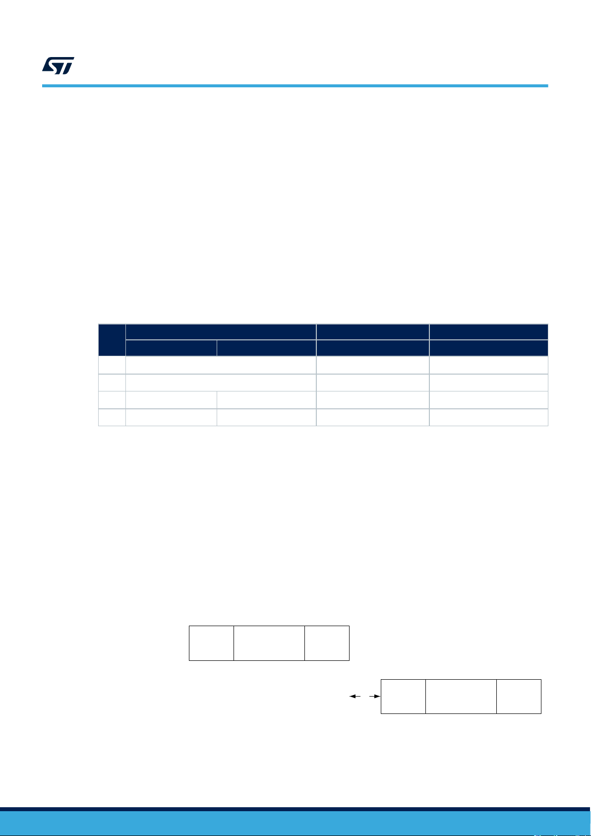
ST25TV02KC ST25TV512C
Timing definition
t2 is also the time after which the VCD may send a new request to the VICC, as described in Figure 8. ISO15693
protocol timing.
Values of t2 are given in Table 97. Timing values.
t3: VCD new request delay when no response is received from the VICC
t3 is the time after which the VCD may send an EOF to switch to the next slot when no response has been
received from the VICC after an Inventory request with Nb_slots_flag set to 0.
The EOF sent by the VCD may be either 10% or 100% modulated regardless of the modulation index used for
transmitting the VCD request to the VICC.
Starting from the rising edge of the request EOF sent by the VCD:
• If this EOF is 100% modulated, the VCD waits for a time at least equal to t3min for 100% modulation before
sending a new EOF.
• If this EOF is 10% modulated, the VCD waits for a time at least equal to t3min for 10%
• modulation before sending a new EOF.
Table 97. Timing values
-
Minimum (min) values Nominal (nom) values Maximum (max) values
100% modulation 10% modulation
t
1
t
2
t
3
t
EOF
t
1max
4320 / fC = 318.6 µs 4352 / fC = 320.9 µs
4192 / fC = 309.2 µs
(2)
(3)
+t
SOF
t
1max
(2)
(4)
+t
+t
NRT
2min
10 ms No
4384 / fC = 323.3 µs
No No
No t
3nom
t
EOFnom
No t
20 ms
3max
1. VCD request will not be interpreted during the first milliseconds following the field rising.
2. t
3. t
does not apply for write-alike commands. Specific timing constraints for write-alike commands are defined by Wt and
1max
t
(see below)
EOF
is the time taken by the VICC to transmit an SOF to the VCD. t
SOF
depends on the response data rate: High data rate
SOF
or Low data rate.
4. t
is the nominal response time of the VICC. t
NRT
and the size of expected response frame.
depends on the response data rate, the subcarrier modulation mode,
NRT
Wt: VICC response delay for write-alike commands with Option_flag=0
For a write-alike command with option_flag=0, for instance a command involving a programmation of the
EEPROM, the VICC waits for a time Wt starting at the rising edge of the EOF in the request received from
the VCD, before transmitting its response.
The Wt time is equal to t
+ a multiple of 4096 / fC (= 302 μs).
1nom
Figure 12. Write-alike frame exchange between VCD and ST25TVxxxC when Option_flag=0
(1)
DS13304 - Rev 3
VCD
ST25TVxxxC
SOF
Write-alike
request
(Option_flag=0)
EOF
W
SOF
t
Write-alike
response
EOF
page 45/87
Page 46

t
: EOF request delay for write-alike commands with Option_flag=1
EOF
ST25TV02KC ST25TV512C
Timing definition
For a write-alike command with Option_flag=1, the VCD waits for a time t
starting at the rising edge of the
EOF
EOF in the request frame, before sending an isolated EOF request which triggers the response of the VICC.
Upon reception of the isolated EOF request, the VICC waits for a time t1 starting at the rising edge of the isolated
EOF request, before transmitting its response.
Authorized values of t
are given in Table 97. Timing values.
EOF
Figure 13. Write-alike frame exchange between VCD and ST25TVxxxC when Option_flag=1
VCD
ST25TVxxxC
Write-alike
SOF EOF
request
(Option_flag=1)
EOF
t
EOF
t
SOF
1
Write-alike
response
EOF
DS13304 - Rev 3
page 46/87
Page 47

6.4 RF commands
The ST25TVxxxC supports the following RF command set:
• Inventory, used to perform the anticollision sequence.
• StayQuiet, used to put the ST25TVxxxC in QUIET state, where it responds only to commands in Addressed
mode.
• ReadSingleBlock, used to read the 32 bits of a block and its locking status.
• WriteSingleBlock, used to write and verify the new content for an update of a 32 bits block, provided that
the write access is granted.
• LockBlock, used to permanently forbid the write access to the selected block.
• ReadMultipleBlocks, used to read the content of a range of blocks and their locking status.
• Select, used to put the ST25TVxxxC in SELECTED state. After this command, the ST25TVxxxC processes
all commands requested with Select_flag set.
• ResetToReady, used to put the ST25TVxxxC in the READY state.
• WriteAFI, used to write an 8-bit value in the AFI register.
• LockAFI, used to lock the AFI register.
• WriteDSFID, used to write an 8-bit value in the DSFID register.
• LockDSFID, used to lock the DSFID register.
• GetSystemInfo and ExtendedGetSystemInfo, used to read the standard system information values.
• GetMultipleBlockSecurityStatus, used to read the security status of a range blocks.
• ReadConfig, used to read configuration registers.
• WriteConfig, used to write configuration registers.
• Kill, used to permanently deactivate the tag by entering the KILLED state.
• WritePassword, used to change password of an open security session.
• PresentPassword, used to open a security session.
• GetRandomNumber, used to generate a 16 bit number.
• ToggleUntraceable, used to enter or leave the UNTRACEABLE state.
• Initiate, used to set the Initiate_flag register to 1.
• InventoryInitiated, used to perform the anticollision sequence on ST25TVxxxC with Initiate_flag set to 1.
Their codes are given in Table 98.
ST25TV02KC ST25TV512C
RF commands
Table 98. Command code
Opcode
01h Inventory 2Bh GetSystemInfo
02h StayQuiet 2Ch GetMultipleBlockSecurityStatus
20h ReadSingleBlock 3Bh ExtendedGetSystemInfo
21h WriteSingleBlock A0h ReadConfig
22h LockBlock A1h WriteConfig
23h ReadMultipleBlocks A6h Kill
25h Select B1h WritePassword
26h ResetToReady B3h PresentPassword
27h WriteAFI B4h GetRandomNumber
28h LockAFI BAh ToggleUntraceable
29h WriteDSFID D1h InventoryInitiated
2Ah LockDSFID D2h Initiate
Command Opcode Command
DS13304 - Rev 3
page 47/87
Page 48

6.4.1 Inventory
When receiving the Inventory request, the ST25TVxxxC sends a response if the parameters match the values of
the UID and AFI registers.
Inventory_ flag is set to 1 : bits 4 and 5 of Request_flags respectively code AFI_flag and Nb_slots_flag.
Option_flag is set to 0 : no option supported.
SOF
- 00xx01xxb 01h 8 bits 8 bits 0-64 bits 16 bits -
1. AFI field present when Request_flags=00x101xxb
Request parameters and data include :
• AFI parameter if AFI_flag is set to 1
• Mask_length in bits, ≤ 60 when Nb_slots_flag = 0b, ≤ 64 when Nb_slots_flag = 1b
• Mask_value, size in bytes is (Mask_length + 7)/8, not present if Mask_length = 00h
Table 99. Inventory request format
Request_flags Opcode
Table 100. Inventory response format
AFI
ST25TV02KC ST25TV512C
RF commands
(1)
Mask_length Mask_value CRC_B EOF
SOF Response_flags DSFID UID CRC_B EOF
- 00h 8 bits 64 bits 16 bits -
When Error_flag is set to 0, response data include :
• DSFID register value
• UID register value
The ST25TVxxxC does not generate any answer in case of error.
When the VICC responds to an Inventory request, the timing of the frame exchange is that of a read-alike
command as depicted in Figure 11. Read-alike frame exchange between VCD and ST25TVxxxC.
When Nb_slots_flag is set to 0, the VCD issues 15 EOF requests after the initial request from Table 99. Inventory
request format, with the following timings described in Section 6.3 Timing definition:
• if the VICC responds to an EOF request, the timing of the frame exchange is that of a readalike command
• if the VCD receives a response from one or more VICCs, it waits for a time t2 before sending the next EOF
request
• if the VCD does not receive a response from any VICC, it waits for a time t3 before sending the next EOF
request
6.4.2 StayQuiet
When receiving the StayQuiet request:
• the ST25TVxxxC enters the QUIET state if no error occurs, and does NOT send back a response.
• there is NO response to the StayQuiet command even if an error occurs.
Select_flag is set to 0 and Address_flag is set to 1 : the StayQuiet request must be issued in Addressed mode.
Option_flag is set to 0 : no option supported.
DS13304 - Rev 3
Table 101. StayQuiet request format
SOF Request_flags Opcode UID CRC_B EOF
- 001000xxb 02h 64 bits 16 bits -
Request parameters and data include :
• UID parameter
page 48/87
Page 49

ST25TV02KC ST25TV512C
When in QUIET state:
• the ST25TVxxxC does not process any request if Inventory_flag is set to 1,
• the ST25TVxxxC processes only requests with Address_flag set to 1.
The ST25TVxxxC exits the QUIET state:
• when it is reset (power off).
• on a successful Select request, it then goes to the SELECTED state.
• on a successful ResetToReady request, it then goes to the READY state.
Figure 14. Stay Quiet frame
RF commands
VCD
ST25TVxxxC
6.4.3 ReadSingleBlock
When receiving the ReadSingleBlock request, the ST25TVxxxC reads the requested block and sends back its
32-bit value in the response.
ReadSingleBlock command is applicable and successful, if and only if the requested block is available and has
granted read access (ie, parent area not protected in Read or security session open).
When Option_flag is set to 1, the Block Security Status of the requested block is included in the response.
SOF
- 0xxx00xxb 20h 64 bits 8 bits 16 bits -
1. UID field present when Request_fllags=0x1000xxb
Request parameters and data include :
• UID parameter if Address_flag is set to 1
• Block_number coded on 1 byte
Request_flags Opcode
SOF
Stay Quiet
request
Table 102. ReadSingleBlock request format
UID
(1)
Block_number CRC_B EOF
EOF
Table 103. ReadSingleBlock response format when Error_flag equals 0
SOF
- 00h 8 bits 32 bits 16 bits -
1. BSS field present when Request_flags=01xx00xxb.
Response_flags
BSS
(1)
Data CRC_B EOF
When Error_flag is set to 0, response data include :
• Block security status if Option_flag is set to 1 (see Table 31. Block security status)
• Four bytes of block data
Note: The Data field from Table 103 may be impacted by the ANDEF feature (see Section 5.4.2 Augmented NDEF
description)
When Error_flag is set to 1, Error_code field may take the values of Table 104 in a ReadSingleBlock response.
DS13304 - Rev 3
page 49/87
Page 50

Error code Description
02h Invalid request format
03h Invalid Request_flags value
10h Requested block not available
15h Read access to requested block is protected and security session is closed
When the VICC responds to a ReadSingleBlock request, the timing of the frame exchange is that of a read-alike
command as depicted in Figure 11. Read-alike frame exchange between VCD and ST25TVxxxC.
6.4.4 WriteSingleBlock
When receiving the WriteSingleBlock request, the ST25TVxxxC writes the data contained in the request to the
targeted block and reports whether the write operation was successful in the response.
WriteSingleBlock command is applicable and successful, if and only if the requested block is available and has
granted write access (ie, the block is not locked, area not protected in Write or security session open).
When Option_flag is set to 1, the response is postponed to the subsequent EOF request.
SOF
- 0xxx00xxb 21h 64 bits 8 bits 32 bits 16 bits -
1. UID field present when Request_fllags=0x1000xxb
Request_flags Opcode
ST25TV02KC ST25TV512C
Table 104. ReadSingleBlock error codes when Error_flag equals 1
Table 105. WriteSingleBlock request format
UID
(1)
Block_number Data CRC_B EOF
RF commands
Request parameters and data include :
• UID parameter if Address_flag is set to 1
• Block_number coded on 1 byte
• Four bytes of block data
Note: The Data field from Table 105 is not impacted by the ANDEF feature (see Section 5.4.2 Augmented NDEF
description)
Table 106. WriteSingleBlock response format when Error_flag equals 0
SOF
- 00h 16 bits -
Response_flags CRC_B EOF
When Error_flag is set to 0, no data is inserted between the Response_flags and CRC_B fields.
When Error_flag is set to 1, Error_code field may take the values of Table 107 in a WriteSingleBlock response.
Table 107. WriteSingleBlock error codes when Error_flag equals 1
Error code
02h Invalid request format
03h Invalid Request_flags value
10h Requested block not available
12h Write access to requested block is protected and security session is closed
13h Programmation of requested block failed
Description
DS13304 - Rev 3
When the VICC responds to a WriteSingleBlock request, the timing of the frame exchange is that of a write-alike
command as depicted in Figure 12 and Figure 13.
page 50/87
Page 51

During the RF write cycle Wt, there should be no modulation (neither 100% nor 10%), otherwise the ST25TVxxxC
may not correctly program the data into the memory.
6.4.5 LockBlock
When receiving the LockBlock request, the ST25TVxxxC locks the corresponding block value permanently to
protect its content against new writing.
LockBlock command is applicable and successful, if and only if the requested block is available and has granted
write access (ie, the block is not locked, area not protected in Write or security session open).
When Option_flag is set to 1, the response is postponed to the subsequent EOF request.
SOF
- 0xxx00xxb 22h 64 bits 8 bits 16 bits -
1. UID field present when Request_flags =0x1000xxb
Request parameters and data include :
• UID parameter if Address_flag is set to 1
• Block_number coded on 1 byte
Table 108. LockBlock request format
Request_flags Opcode
UID
ST25TV02KC ST25TV512C
RF commands
(1)
Block_number CRC_B EOF
Table 109. LockBlock response format when Error_flag equals 0
SOF Response_flags CRC_B EOF
- 00h 16 bits -
When Error_flag is set to 0, no data is inserted between the Response_flags and CRC_B fields.
When Error_flag is set to 1, Error_code field may take the values of Table 110 in a LockBlock response.
Table 110. LockBlock error codes when Error_flag equals 1
Error code
02h Invalid request format
03h Invalid Request_flags value
10h Requested block not available
11h Requested block is already locked
12h Write access to requested block is protected and security session is closed
14h Lock of requested block failed
Description
When the VICC responds to a LockBlock request, the timing of the frame exchange is that of a write-alike
command as depicted in Figure 12 and Figure 13.
During the RF write cycle Wt, there should be no modulation (neither 100% nor 10%), otherwise the ST25TVxxxC
may not correctly program the LCK_BLOCK register into the memory.
6.4.6 ReadMultipleBlocks
When receiving the ReadMultipleBlocks request, the ST25TVxxxC reads the selected blocks and sends back
their value in multiples of 32 bits in the response.
ReadMultipleBlocks command is applicable and successful, if and only if the first block requested is available and
has granted read access (ie, parent area not protected in Read or security session open).
When the requested range of blocks ends beyond the user memory or in an area without read access authorized,
the range of blocks used for the response data is truncated before the first block not available / not readable.
When Option_flag is set to 1, the Block Security Status of the blocks read are included in the response.
DS13304 - Rev 3
page 51/87
Page 52

ST25TV02KC ST25TV512C
RF commands
Table 111. ReadMultipleBlocks request format
SOF Request_flags Opcode
- 0xxx00xxb 23h 64 bits 8 bits 8 bits 16 bits -
1. UID field present when Request_flags=0x1000xxb
Request parameters and data include :
• UID parameter if Address_flag is set to 1
• Block_number coded on 1 byte, requested range of blocks starts at Block_number
• Additional_blocks coded on 1 byte, requested range of blocks ends at Block_number + Additional_blocks
Table 112. ReadMultipleBlocks response format when Error_flag equals 0
SOF
- 00h
1. BSS field present when Request_flags=01xx00xxb
2. Repeated as needed
Response_flags
When Error_flag is set to 0, response data include for each block :
• Block security status if Option_flag is set to 1 (see Table 31. Block security status)
• Four bytes of block data
Note: The Data field from Table 112 may be impacted by the ANDEF feature (see Section 5.4.2 Augmented NDEF
description)
When Error_flag is set to 1, Error_code field may take the values of Table 113 in a ReadMultipleBlocks response.
UID
(1)
Block_number Additional_blocks CRC_B EOF
BSS
8 bits
(1)
(2)
Data CRC_B EOF
32 bits
(2)
16 bits -
Error code
When the VICC responds to a ReadMultipleBlocks request, the timing of the frame exchange is that of a
read-alike command as depicted in Figure 11. Read-alike frame exchange between VCD and ST25TVxxxC.
6.4.7 Select
When receiving the Select request:
• If the UID parameter matches its own UID, the ST25TVxxxC enters or stays in the SELECTED state and
sends a response.
• If the UID parameter does not match its own UID, the selected ST25TVxxxC returns to the READY state and
does not send a response.
• If an error occurs, the ST25TVxxxC remains in its current state.
Select_flag is set to 0 and Address_flag is set to 1 : the Select request must be issued in Addressed mode.
Option_flag is set to 0 : no option supported.
Table 113. ReadMultipleBlocks error codes when Error_flag equals 1
Description
02h Invalid request format
03h Invalid Request_flags value
10h Requested block not available
15h Read access to requested block is protected and security session is closed
Table 114. Select request format
DS13304 - Rev 3
SOF Request_flags Opcode UID CRC_B EOF
- 001000xxb 25h 64 bits 16 bits -
page 52/87
Page 53

ST25TV02KC ST25TV512C
RF commands
Request parameters and data include :
• UID parameter
Table 115. Select response format when Error_flag equals 0
SOF Response_flags CRC_B EOF
- 00h 16 bits -
• When Error_flag is set to 0, no data is inserted between the Response_flags and CRC_B fields.
• When Error_flag is set to 1, Error_code field may take the values of Table 116 in a Select response.
Table 116. Select error codes when Error_flag equals 1
Error code Description
02h Invalid request format
03h Invalid Request_flags value
When the VICC responds to a Select request, the timing of the frame exchange is that of a read-alike command
as depicted inFigure 11. Read-alike frame exchange between VCD and ST25TVxxxC.
6.4.8 ResetToReady
When receiving the ResetToReady request:
• the ST25TVxxxC enters or stays in the READY state if no error occurs.
• in SELECTED state, the ST25TVxxxC responds an error when Addressed mode is used.
• in QUIET state, the ST25TVxxxC handles the request even if Non-addressed mode is used.
• If an error occurs, the ST25TVxxxC remains in its current state.
Option_flag is set to 0 : no option supported.
SOF
- 00xx00xxb 26h 64 bits 16 bits -
1. UID field present when Request_flags=0x1000xxb
Request parameters and data include:
• UID parameter if Address_flag is set to 1
SOF Response_flags CRC_B EOF
- 00h 16 bits -
Table 117. ResetToReady request format
Request_flags Opcode
UID
(1)
CRC_B EOF
Table 118. ResetToReady response format when Error_flag equals 0
DS13304 - Rev 3
When Error_flag is set to 0, no data is inserted between the Response_flags and CRC_B fields.
When Error_flag is set to 1, Error_code field may take the values of Table 119 in a ResetToReady response.
Table 119. ResetToReady error codes when Error_flag equals 1
Error code
02h Invalid request format
03h Invalid Request_flags value
Description
page 53/87
Page 54

When the VICC responds to a ResetToReady request, the timing of the frame exchange is that of a read-alike
command as depicted in Figure 11. Read-alike frame exchange between VCD and ST25TVxxxC.
6.4.9 WriteAFI
When receiving the WriteAFI request, the ST25TVxxxC programs the 8-bit AFI register.
WriteAFI command is applicable and successful, if and only if the WriteAFI command is allowed (ie, AFI is not
locked, AFI_PROT=0b or AREA1 security session open).
When Option_flag is set to 1, the response is postponed to the subsequent EOF request.
SOF
- 0xxx00xxb 27h 64 bits 8 bits 16 bits -
1. UID field present when Request_flags=0x1000xxb
Request parameters and data include:
• UID parameter if Address_flag is set to 1
• AFI parameter coded on 1 byte, used to program the AFI register
Table 120. WriteAFI request format
Request_flags Opcode
UID
ST25TV02KC ST25TV512C
RF commands
(1)
AFI CRC_B EOF
SOF Response_flags CRC_B EOF
When Error_flag is set to 0, no data is inserted between the Response_flags and CRC_B fields.
When Error_flag is set to 1, Error_code field may take the values of Table 122 in a WriteAFI response.
Error code
02h Invalid request format
03h Invalid Request_flags value
12h LCK_AFI=1b or (AFI_PROT=1b and AREA1 security session is closed)
13h Programmation of AFI register failed
When the VICC responds to a WriteAFI request, the timing of the frame exchange is that of a write-alike
command as depicted in Figure 12 and Figure 13.
During the RF write cycle Wt, there should be no modulation (neither 100% nor 10%), otherwise the ST25TVxxxC
may not correctly program the AFI register into the memory.
6.4.10 LockAFI
When receiving the LockAFI request, the ST25TVxxxC locks the AFI register permanently.
LockAFI command is applicable and successful, if and only if the LockAFI command is allowed (ie, AFI not
already locked, AFI_PROT=0b or AREA1 security session open).
When Option_flag is set to 1, the response is postponed to the subsequent EOF request.
Table 121. WriteAFI response format when Error_flag equals 0
- 00h 16 bits -
Table 122. WriteAFI error codes when Error_flag equals 1
Description
DS13304 - Rev 3
Table 123. LockAFI request format
SOF
- 0xxx00xxb 28h 64 bits 16 bits -
Request_flags Opcode
UID
(1)
CRC_B EOF
page 54/87
Page 55

ST25TV02KC ST25TV512C
1. UID field present when Request_flags=0x1000xxb
Request parameters and data include :
• UID parameter if Address_flag is set to 1
Table 124. LockAFI response format when Error_flag equals 0
SOF Response_flags CRC_B EOF
- 00h 16 bits -
When Error_flag is set to 0, no data is inserted between the Response_flags and CRC_B fields.
When Error_flag is set to 1, Error_code field may take the values of Table 125 in a LockAFI response.
Table 125. LockAFI error codes when Error_flag equals 1
Error code Description
02h Invalid request format
03h Invalid Request_flags value
11h LCK_AFI=1b : Successful LockAFI command already occured
12h AFI_PROT=1b and AREA1 security session is closed
14h Programmation of LCK_AFI register failed
RF commands
When the VICC responds to a LockAFI request, the timing of the frame exchange is that of a write-alike command
as described in Figure 12 and Figure 13.
During the RF write cycle Wt, there should be no modulation (neither 100% nor 10%), otherwise the ST25TVxxxC
may not correctly program the LCK_AFI register into the memory.
6.4.11 WriteDSFID
When receiving the WriteDSFID request, the ST25TVxxxC programs the 8-bit DSFID register. WriteDSFID
command is applicable and successful, if and only if the DSFID register is not locked (LCK_DSFID=0b).
When Option_flag is set to 1, the response is postponed to the subsequent EOF request.
SOF
- 0xxx00xxb 29h 64 bits 8 bits 16 bits -
1. UID field present when Request_flags=0x1000xxb
Request parameters and data include:
• UID parameter if Address_flag is set to 1.
• DSFID parameter coded on 1 byte, used to program the DSFID register
SOF Response_flags CRC_B EOF
- 00h 16 bits -
Table 126. WriteDSFID request format
Request_flags Opcode
UID
(1)
DSFID CRC_B EOF
Table 127. WriteDSFID response format when Error_flag equals 0
DS13304 - Rev 3
When Error_flag is set to 0, no data is inserted between the Response_flags and CRC_B fields.
When Error_flag is set to 1, Error_code field may take the values of Table 128 in a WriteDSFID response.
page 55/87
Page 56

Error code Description
When the VICC responds to a WriteDSFID request, the timing of the frame exchange is that of a write-alike
command as described in Figure 12 and Figure 13.
During the RF write cycle Wt, there should be no modulation (neither 100% nor 10%), otherwise the ST25TVxxxC
may not correctly program the DSFID register into the memory.
6.4.12 LockDSFID
When receiving the LockDSFID request, the ST25TVxxxC locks the DSFID register permanently. LockDSFID
command is applicable and successful, if and only if the DSFID register is not already locked (LCK_DSFID=0b).
When Option_flag is set to 1, the response is postponed to the subsequent EOF request.
SOF
- 0xxx00xxb 2Ah 64 bits 16 bits -
1. UID field present when Request_flags=0x1000xxb
Table 128. WriteDSFID error codes when Error_flag equals 1
02h Invalid request format
03h Invalid Request_flags value
12h LCK_DSFID=1b : DSFID register is locked
13h Programmation of DSFID register failed
Table 129. LockDSFID request format
Request_flags Opcode
ST25TV02KC ST25TV512C
RF commands
UID
(1)
CRC_B EOF
Request parameters and data include:
• UID parameter if Address_flag is set to 1
Table 130. LockDSFID response format when Error_flag equals 0
SOF Response_flags CRC_B EOF
- 00h 16 bits -
When Error_flag is set to 0, no data is inserted between the Response_flags and CRC_B fields.
When Error_flag is set to 1, Error_code field may take the values of Table 131 in a LockDSFID response.
Table 131. LockDSFID error codes when Error_flag equals 1
Error code
02h Invalid request format
03h Invalid Request_flags value
11h LCK_DSFID=1b : Successful LockDSFID command already occured
14h Programmation of LCK_DSFID register failed
Description
When the VICC responds to a LockDSFID request, the timing of the frame exchange is that of a write-alike
command as depicted in Figure 12 and Figure 13.
During the RF write cycle Wt, there should be no modulation (neither 100% nor 10%), otherwise the ST25TVxxxC
may not correctly program the LCK_DSFID register into the memory.
DS13304 - Rev 3
page 56/87
Page 57

6.4.13 GetSystemInfo
When receiving the GetSystemInfo request, the ST25TVxxxC sends back its information data in the response.
Option_flag is set to 0 : no option supported.
SOF Request_flags Opcode
- 00xx00xxb 2Bh 64 bits 16 bits -
1. UID field present when Request_flags=0x1000xxb
Request parameters and data include:
• UID parameter if Address_flag is set to 1
SOF Response_flags Information_flags UID DSFID AFI Memory_size IC_ref CRC_B EOF
- 00h 0Fh 64 bits 8 bits 8 bits 16 bits 08h 16 bits -
When Error_flag is set to 0, response data include :
• Information_flags coded on 1 byte, set to 0Fh (DSFID, AFI, Memory_size and IC_ref fields are all present).
• UID register value
• DSFID register value
• AFI register value
• Memory_size coded on 2 bytes:
– 8-MSB (03h) = Block size in number of Bytes - 1
– 8-LSB (END_MEM) = User memory size in number of Blocks - 1
• IC_REF register value
When Error_flag is set to 1, Error_code field may take the values of Table 134 in a GetSystemInfo response.
ST25TV02KC ST25TV512C
Table 132. GetSystemInfo request format
(1)
UID
Table 133. GetSystemInfo response
RF commands
CRC_B EOF
Table 134. GetSystemInfo error codes when Error_flag equals 1
Error code
02h Invalid request format
03h Invalid Request_flags value
When the VICC responds to a GetSystemInfo request, the timing of the frame exchange is that of a read-alike
command as depicted in Figure 11.
6.4.14 GetMultipleBlockSecurityStatus
When receiving the GetMultipleBlockSecurityStatus request, the ST25TVxxxC responds the block security status
of the selected blocks.
GetMultipleBlockSecurityStatus command is applicable and successful, if and only if the first block requested is
available.
When the requested range of blocks ends beyond the user memory, the range of blocks used for the response
data is truncated to the last block available.
Option_flag is set to 0 : no option supported.
Description
DS13304 - Rev 3
page 57/87
Page 58

ST25TV02KC ST25TV512C
RF commands
Table 135. GetMultipleBlockSecurityStatus request format
SOF Request_flags Opcode
- 00xx00xxb 2Ch 64 bits 8 bits 8 bits 16 bits -
1. UID field present when Request_flags=0x1000xxb
Request parameters and data include :
• UID parameter if Address_flag is set to 1
• Block_number coded on 1 byte, requested range of blocks starts at Block_number
• Additional_blocks coded on 1 byte, requested range of blocks ends at Block_number + Additional_blocks
Table 136. GetMultipleBlockSecurityStatus response format when Error_flag equals 0
SOF Response_flags BSS CRC_B EOF
- 00h
1. Repeated as needed
When Error_flag is set to 0, response data include for each block :
• Block security status (see Table 31. Block security status)
When Error_flag is set to 1, Error_code field may take the values of Table 137 in a
GetMultipleBlockSecurityStatus response.
UID
(1)
Block_number Additional_blocks CRC_B EOF
8 bits
(1)
16 bits -
Table 137. GetMultipleBlockSecurityStatus error codes when Error_flag equals 1
Error code
02h Invalid request format
03h Invalid Request_flags value
10h Requested block not available
When the VICC responds to a GetMultipleBlockSecurityStatus request, the timing of the frame exchange is that of
a read-alike command as depicted in Figure 11.
6.4.15 ExtendedGetSystemInfo
When receiving the ExtendedGetSystemInfo request, the ST25TVxxxC sends back its information data in the
response.
Option_flag is set to 0 : no option supported.
SOF
- 00xx00xxb 3Bh 0xx1xxxxb 64 bits 16 bits -
1. UID field present when Request_flags=0x1000xxb
Request parameters and data include :
• Information_request_list parameter coded on 1 byte, see Table 139 below
• UID parameter if Address_flag is set to 1
Request_flags Opcode Information_request_list
Description
Table 138. ExtendedGetSystemInfo request format
UID
(1)
CRC_B EOF
DS13304 - Rev 3
page 58/87
Page 59

ST25TV02KC ST25TV512C
Table 139. Information_request_list content
Bit Requested information Description
b0 DSFID
b1 AFI
b2 Memory_size
b3 IC_ref
b4 MOI 1: Information on MOI always returned in response flag
b5 Command_list
b6 CSI information
b7 Ext_list 0: size of Information_request_list is 1 byte
0: DSFID not requested
1: DSFID requested
0: AFI not requested
1: AFI requested
0: VICC memory size not requested
1: VICC memory size requested
0: IC reference not requested
1: IC reference requested
0: list of supported commands not requested
1: list of supported commands requested
0: CSI list not requested
1: CSI list requested
RF commands
Table 140. ExtendedGetSystemInfo response format when Error_flag equals 0
SOF
- 00h 00x0xxxxb 64 bits up to 80 bits 16 bits -
Response_flags Information_flags UID Information_fields CRC_B EOF
Table 141. Information_flags content
Bit
b0 DSFID
b1 AFI
b2 Memory_size
b3 IC_ref
b4 MOI 0: 1 byte addressing
b5 Command_list
b6 CSI_information 0: CSI list not present
b7 Ext_info 0: size of Information_flags is 1 byte
Responded information Description
0: DSFID not present in Information_fields
1 : DSFID present in Information_fields
0: AFI not present in Information_fields
1: AFI present in Information_fields
0: Memory_size not present in Information_fields
1: Memory_size present in Information_fields
0: IC_ref not present in Information_fields
1: IC_ref present in Information_fields
0: Command_list not present in Information_fields
1: Command_list present in Information_fields
DS13304 - Rev 3
Table 142. Information_fields content
(1)
DSFID
8 bits 8 bits 24 bits 08h 00003FEFh
1. Presence of information fields depends on value of Information_flags
AFI
(1)
Memory_size
(1)
IC_ref
(1)
Command_list
(1)
page 59/87
Page 60

ST25TV02KC ST25TV512C
RF commands
When Error_flag is set to 0, response data include :
• Information_flags coded on 1 byte, defining which fields are present (see Table 141)
• UID register value
• DSFID register value, present if Information_flags[0]=1b
• AFI register value, present if Information_flags[1]=1b
• VICC Memory size coded on 3 bytes, present if Information_flags[2]=1b
– 8-MSB (03h) = Block size in number of Bytes - 1
– 16-LSB (END_MEM) = User memory size in number of Blocks - 1
• IC_REF register value, present if Information_flags[3]=1b
• VICC Command list coded on 4 bytes, present if Information_flags[5]=1b
When Error_flag is set to 1, Error_code field may take the values of Table 143 in an ExtendedGetSystemInfo
response.
Table 143. ExtendedGetSystemInfo error codes when Error_flag equals 1
Error code Description
02h Invalid request format
03h Invalid Request_flags or Information_request_list value
When the VICC responds to an ExtendedGetSystemInfo request, the timing of the frame exchange is that of a
read-alike command as depicted in Figure 11.
6.4.16 ReadConfiguration
When receiving the ReadConfiguration request, the ST25TVxxxC reads the selected configuration register and
sends back its value in the response.
ReadConfiguration command is applicable and successful, if and only if the requested configuration register
(identified by the FID/PID pair) is available and has granted read access (i.e. read not protected, or feature not
locked and CONFIG security session open).
Option_flag is set to 0 : no option supported.
SOF
- 00xx00xxb A0h 02h 64 bits 8 bits 8 bits 16 bits -
1. UID field present when Request_flags=0x1000xxb
Request parameters and data include :
• IC manufacturer code coded on 1 byte, value shall be 02h
• UID parameter if Address_flag is set to 1
• FID parameter coded on 1 byte
• PID parameter coded on 1 byte
Request_flags Opcode IC Mfg code
Table 144. ReadConfiguration request format
UID
(1)
FID PID CRC_B EOF
DS13304 - Rev 3
Table 145. ReadConfiguration response format when Error_flag equals 0
SOF
- 00h 8 to 64 bits 16 bits -
1. Size of data responded depends on the requested FID and PID values according to Table 4. List of configuration registers
Response_flags
Data
(1)
CRC_B EOF
When Error_flag is set to 0, response data include :
• Configuration register value coded on 1 to 8 bytes depending on the requested FID/PID pair (see
Table 4. List of configuration registers)
page 60/87
Page 61

ST25TV02KC ST25TV512C
RF commands
Note: When a register value is coded on several bytes, it is transmitted in LSB to MSB byte order in the response to a
ReadConfiguration request.
When Error_flag is set to 1, Error_code field may take the values of Table 146 in a ReadConfiguration response.
Table 146. ReadConfiguration error codes when Error_flag equals 1
Error code Description
01h Invalid IC Mfg code value
02h Invalid request format
03h Invalid Request_flags value
10h Requested FID/PID not available
15h Read access to requested FID/PID is protected and CONFIG security session is closed
When the VICC responds to a ReadConfiguration request, the timing of the frame exchange is that of a read-alike
command as depicted in Figure 11.
6.4.17 WriteConfiguration
When receiving the WriteConfiguration request, the ST25TVxxxC writes the data contained in the request to the
selected configuration register and responds an acknowledgement if the write operation was successful.
WriteConfiguration command is applicable and successful, if and only if the requested configuration register
(identified by the FID/PID pair) is available and has granted write access (i.e. feature not locked and CONFIG
security session open).
When Option_flag is set to 1, the response is postponed to the subsequent EOF request.
Table 147. WriteConfiguration request format
SOF
1. UID field present when Request_flags=0x1000xxb
Request_flags Opcode IC Mfg code
- 0xxx00xxb A1h 02h 64 bits 8 bits 8 bits 8-32 bits 16 bits -
UID
(1)
FID PID Data CRC_B EOF
Request parameters and data include :
• IC manufacturer code coded on 1 byte, value shall be 02h
• UID parameter if Address_flag is set to 1
• FID parameter coded on 1 byte
• PID parameter coded on 1 byte
• New register value coded on 1 to 4 bytes depending on the requested FID/PID pair (see Table 4. List of
configuration registers)
Note: When a register value is coded on several bytes, it is transmitted in LSB to MSB byte order in the
WriteConfiguration request.
Table 148. WriteConfiguration response format when Error_flag equals 0
SOF
- 00h 16 bits -
Response_flags CRC_B EOF
When Error_flag is set to 0:
• no data is inserted between the Response_flags and CRC_B fields.
• the update of the register value into the memory is successful, and the new value is immediately readable
with a ReadConfiguration request. However the effect of the new value may be active immediately or on the
next RF boot sequence depending on the selected configuration (see column Activation time of Table 4. List
of configuration registers).
DS13304 - Rev 3
page 61/87
Page 62

ST25TV02KC ST25TV512C
RF commands
When the effect of a new configuration register value is activated on the next RF boot sequence, the effect of the
former configuration value lasts after the update of the register into the memory until the ST25TVxxxC is put in
POWER-OFF state.
When Error_flag is set to 1, Error_code field may take the values of Table 149 in a WriteConfiguration response.
Table 149. WriteConfiguration error codes when Error_flag equals 1
Error code Description
01h Invalid IC Mfg code value
02h Invalid request format
03h Invalid Request_flags value
10h Requested FID/PID not available
11h Bit of LCK_CONFIG (FID=FFh,PID=00h) already set to 1b
12h Write access to requested FID/PID is protected and CONFIG security session is closed
13h Programmation of requested FID/PID (other than LCK_CONFIG) failed
14h Programmation of LCK_CONFIG (FID=FFh,PID=00h) failed
When the VICC responds to a WriteConfiguration request, the timing of the frame exchange is that of a write-alike
command as depicted in Figure 12 and Figure 13.
During the RF write cycle Wt, there should be no modulation (neither 100% nor 10%), otherwise the ST25TVxxxC
may not correctly program the configuration register into the memory.
6.4.18 WritePassword
When receiving the WritePassword request, the ST25TVxxxC uses the data contained in the request to modify
the selected password and responds an acknowledgement if the write operation was successful.
WritePassword command is applicable and successful, if and only if it preceded by a successful PresentPassword
command with same password selected. Refer to Section 5.1.2 Password management for details on password
management.
When Option_flag is set to 1, the response is postponed to the subsequent EOF request.
SOF
1. UID field present when Request_flags=0x1000xxb
Request parameters and data include :
• IC manufacturer code coded on 1 byte, value shall be 02h
• UID parameter if Address_flag is set to 1
• Password_id coded on 1 byte
• Password_data coded on 4 or 8 bytes according to Table 27. List of password registers
The Password_data value is obtained from the encryption of the new plain value of the password as
described in Section 5.1.3 Password encryption.
Request_flags Opcode IC Mfg code
- 0xxx00xxb B1h 02h 64 bits 8 bits 32 or 64 bits 16 bits -
Table 150. WritePassword request format
(1)
UID
Password_id Password_data CRC_B EOF
DS13304 - Rev 3
page 62/87
Page 63

ST25TV02KC ST25TV512C
RF commands
Danger:
If a plain value is mistakenly used in the Password_data field of the WritePassword command, the
presentation of its encrypted value with the PresentPassword command fails on the ST25TVxxxC
device.
Note: The behavior of the WritePassword command is different between the ST25TVxxx and ST25TVxxxC devices
regarding the encryption of the Password_data field. The Password_data field is a plain password value on
the ST25TVxxx device described in datasheet DS12074, while it is an encrypted password value on the
ST25TVxxxC device described in this document.
It is recommended to issue the WritePassword request in Addressed or Select mode, in order to improve the
system robustness.
This ensures that password change is only applied to a specific tag/UID.
Table 151. WritePassword response format when Error_flag equals 0
SOF Response_flags CRC_B EOF
- 00h 16 bits -
When Error_flag is set to 0:
• no data is inserted between the Response_flags and CRC_B fields.
• the update of the password into the memory is successful, and the corresponding security session remains
open.
When Error_flag is set to 1, Error_code field may take the values of Table 152 in a WritePassword response.
Table 152. WritePassword error codes when Error_flag equals 1
Error code
01h Invalid IC Mfg code value
02h Invalid request format, including case of invalid password size
03h Invalid Request_flags value
10h Invalid Password_id value
12h Security session is closed
13h Programmation of requested password failed
Description
When the VICC responds to a WritePassword request, the timing of the frame exchange is that of a write-alike
command as depicted in Figure 12 and Figure 13.
During the RF write cycle Wt, there should be no modulation (neither 100% nor 10%), otherwise the ST25TVxxxC
may not correctly program the password value into the memory.
There is no anti-tearing mechanism while operating the WritePassword command. Command should be applied
with stable RF field, otherwise the write operation may not complete properly, and could imply a loss/corruption of
password content.
The ST25TVxxxC offers a password recovery capability when such content loss/corruption occurs, see
Section 5.1.2 Password management.
DS13304 - Rev 3
page 63/87
Page 64

6.4.19 PresentPassword
When receiving the PresentPassword request, the ST25TVxxxC compares the selected password register with
the password coded in the request and responds an acknowledgment if the operation was successful.
After a successful PresentPassword command, the security session associated to the password is open as
described in Section 5.1 Data protection.
Option_flag is set to 0 : no option supported.
SOF
1. UID field present when Request_flags=001000xxb
Request parameters and data include :
• IC manufacturer code coded on 1 byte, value shall be 02h
• UID parameter if Address_flag is set to 1
• Password_id coded on 1 byte
• Password_data coded on 4 or 8 bytes according to Table 27. List of password registers
The unique valid Password_data value is obtained from the encryption of the plain password value as
described in Section 5.1.3 Password encryption.
It is recommended to issue the PresentPassword request in Addressed or Select mode, in order to improve the
system robustness. This ensures that password presentation is only applied to a specific tag/UID.
Request_flags Opcode IC Mfg code
- 00xx00xxb B3h 02h 64 bits 8 bits 32 or 64 bits 16 bits -
ST25TV02KC ST25TV512C
Table 153. PresentPassword request format
(1)
UID
Password_id Password_data CRC_B EOF
RF commands
Table 154. PresentPassword response format when Error_flag equals 0
SOF
- 00h 16 bits -
Response_flags CRC_B EOF
When Error_flag is set to 0:
• no data is inserted between the Response_flags and CRC_B fields.
• the presentation of the password is successful, and the corresponding security session is open.
When Error_flag is set to 1, Error_code field may take the values of Table 155 in a PresentPassword response.
All security sessions are closed if an invalid value of Password_data is presented.
Warning:
After the presentation of an invalid value of Password_data with the PresentPassword /
Kill / ToggleUntraceable command, the GetRandomNumber command shall be called before
attempting another password presentation with the PresentPassword command as described in
Section 5.1.3 Password encryption.
The ST25TVxxxC offers a password attempt limit capability to protect a password against brute-force attacks, see
Section 5.1.2 Password management.
Table 155. PresentPassword error codes when Error_flag equals 1
Error code
01h Invalid IC Mfg code value
02h Invalid request format, including case of invalid password size
03h Invalid Request_flags value
0Fh Invalid Password_data value
10h Invalid Password_id value
Description
DS13304 - Rev 3
page 64/87
Page 65

When the VICC responds to a PresentPassword request, the timing of the frame exchange is that of a read-alike
command as depicted in Figure 11.
6.4.20 Kill
When receiving the Kill request, the ST25TVxxxC compares register PWD_CFG with the password coded in the
request and responds an acknowledgment if the operation was successful.
Kill command is applicable if and only if the DIS_KILL register is set to 0b, otherwise it is ignored. After a
successful Kill command, the ST25TVxxxC permanently enters the KILLED state, where it stays mute to any
request.
Select_flag is set to 0 and Address_flag is set to 1 : the Kill request must be issued in Addressed mode.
When Option_flag is set to 1, the response is postponed to the subsequent EOF request.
SOF Request_flags Opcode IC Mfg code UID Password_id Password_data CRC_B EOF
Request parameters and data include :
• IC manufacturer code coded on 1 byte, value shall be 02h
• UID parameter
• Password_id coded on 1 byte, value shall be 00h
• Password_data coded on 4 bytes
The unique valid Password_data value is obtained from the encryption of the plain password value as
described in Section 5.1.3 Password encryption
ST25TV02KC ST25TV512C
RF commands
Table 156. Kill request format
- 0x1000xxb A6h 02h 64 bits 00h 32 bits 16 bits -
Warning:
After the presentation of an invalid value of Password_data with the PresentPassword /
Kill / ToggleUntraceable command, the GetRandomNumber command shall be called before
attempting another password presentation with the Kill command.
Note: The behavior of the Kill command is different between the ST25TVxxx and ST25TVxxxC devices regarding the
encryption of the Password_data field. The Password_data field is a plain password value on the ST25TVxxx
device described in datasheet DS12074, while it is an encrypted password value on the ST25TVxxxC device
described in this document.
Table 157. Kill response format when Error_flag equals 0
SOF
- 00h 16 bits -
Response_flags CRC_B EOF
When Error_flag is set to 0:
• no data is inserted between the Response_flags and CRC_B fields.
• the ST25TVxxxC permanently enters the KILLED state by setting the KILL_CMD register to 1b.
When Error_flag is set to 1, Error_code field may take the values of Table 158 in a Kill response.
Table 158. Kill error codes when Error_flag equals 1
Error code
01h Invalid IC Mfg code value
02h Invalid request format
03h Invalid Request_flags value
Description
DS13304 - Rev 3
page 65/87
Page 66

When the VICC responds to a Kill request, the timing of the frame exchange is that of a write-alike command as
depicted in Figure 12 and Figure 13.
During the RF write cycle Wt, there should be no modulation (neither 100% nor 10%), otherwise the ST25TVxxxC
may not correctly program the KILL_CMD register into the memory.
6.4.21 Initiate
When receiving the Initiate request, the ST25TVxxxC sets the Initiate_flag register to 1b and sends back a
response. Initiate_flag is automatically reset to 0b when the ST25TVxxxC enters the POWER-OFF state.
Select_flag is set to 0 and Address_flag is set to 0 : the Initiate request must be issued in Non- addressed mode.
Option_flag is set to 0 : no option supported.
SOF Request_flags Opcode IC Mfg code CRC_B EOF
- 000000xxb D2h 02h 16 bits -
ST25TV02KC ST25TV512C
RF commands
Error code Description
0Fh Invalid Password_data value
10h Invalid Password_id value
14h Programmation of KILL_CMD failed
Table 159. Initiate request format
Request parameters and data include :
• IC manufacturer code coded on 1 byte, value shall be 02h
SOF Response_flags DSFID UID CRC_B EOF
- 00h 8 bits 64 bits 16 bits -
When Error_flag is set to 0, Initiate_flag is set to 1b response data include :
• DSFID register value
• UID register value
The ST25TVxxxC does not generate any answer in case of error.
When the VICC responds to an Initiate request, the timing of the frame exchange is that of a read- alike command
as depicted in Figure 11.
6.4.22 InventoryInitiated
When receiving the InventoryInitiated request, the ST25TVxxxC sends a response if Initiate_flag is set to 1b and
the parameters match the values of the UID and AFI registers.
Inventory_flag is set to 1 : bits 4 and 5 of Request_flags respectively code AFI_flag and Nb_slots_flag.
Option_flag is set to 0 : no option supported.
SOF
1. AFI field present when Request_flags=00x101xxb
Request_flags Opcode IC Mfg code
- 00xx01xxb D1h 02h 8 bits 8 bits 0-64 bits 16 bits -
Table 160. Initiate response format when Error_flag equals 0
Table 161. InventoryInitiated request format
(1)
AFI
Mask_length Mask_value CRC_B EOF
DS13304 - Rev 3
Request parameters and data include :
• IC manufacturer code coded on 1 byte, value shall be 02h
page 66/87
Page 67

ST25TV02KC ST25TV512C
RF commands
• AFI parameter if AFI_flag is set to 1
• Mask_length in bits, ≤ 60 when Nb_slots_flag = 0b, ≤ 64 when Nb_slots_flag = 1b
• Mask_value, size in bytes is (Mask_length + 7)/8, not present if Mask_length = 00h
Table 162. InventoryInitiated response format when Error_flag equals 0
SOF Response_flags DSFID UID CRC_B EOF
- 00h 8 bits 64 bits 16 bits -
When Error_flag is set to 0, response data include :
• DSFID register value
• UID register value
The ST25TVxxxC does not generate any answer in case of error.
When the VICC responds to an InventoryInitiated request, the timing of the frame exchange is that of a read-alike
command as depicted in Figure 11.
When Nb_slots_flag is set to 0, the VCD issues 15 EOF requests after the initial request from Table 161, with the
following timings described in Section 6.3 Timing definition:
• if the VICC responds to an EOF request, the timing of the frame exchange is that of a read-alike command
• if the VCD receives a response from one or more VICCs, it waits for a time t2 before sending the next EOF
request
• if the VCD does not receive a response from any VICC, it waits for a time t3 before sending the next EOF
request
6.4.23 ToggleUntraceable
When receiving the ToggleUntraceable request, the ST25TVxxxC compares register PWD_UNTR with the
password coded in the request and responds an acknowledgement if the operation was successful.
ToggleUntraceable command is applicable only in the following cases, otherwise it is ignored :
• the ST25TVxxxC is in READY, SELECTED or QUIET state, and the request is issued in Addressed mode
(Select_flag=0, Address_flag=1)
• the ST25TVxxxC is in UNTRACEABLE state, and the request is issued in Non-Addressed mode
(Select_flag=0, Address_flag=0)
After a successful ToggleUntraceable command, the ST25TVxxxC leaves or enters (depending on the addressing
mode) the UNTRACEABLE state described in Section 6.2.9 Custom states.
When Option_flag is set to 1, the response is postponed to the subsequent EOF request.
SOF
1. UID field present when Request_flags=0x1000xxb
Request parameters and data include :
• IC manufacturer code coded on 1 byte, value shall be 02h
• UID parameter if Address_flag is set to 1
• Password_id coded on 1 byte, value shall be 03h
• Password_data coded on 4 bytes
The unique valid Password_data value is obtained from the encryption of the plain password value as
described in section 5.1.3
Request_flags Opcode IC Mfg code
- 0xx000xxb BAh 02h 64 bits 03h 32 bits 16 bits -
Table 163. ToggleUntraceable request format
(1)
UID
Password_id Password_data CRC_B EOF
DS13304 - Rev 3
page 67/87
Page 68

ST25TV02KC ST25TV512C
RF commands
Warning:
After the presentation of an invalid value of Password_data with the PresentPassword /
Kill / ToggleUntraceable command, the GetRandomNumber command shall be called before
attempting another password presentation with the ToggleUntraceable command as described
in Section 5.1.3 Password encryption.
Note: Opcode value BAh is used for the EnableUntraceable command of the ST25TVxxx device described in
datasheet DS12074. The EnableUntraceable command has the same request format as the ToggleUntraceable
command, except for the value of the Password_id field which is 00h on the ST25TVxxx device, and 03h on the
ST25TVxxxC device described in this document.
Table 164. ToggleUntraceable response format when Error_flag equals 0
SOF Response_flags CRC_B EOF
- 00h 16 bits -
When Error_flag is set to 0:
• no data is inserted between the Response_flags and CRC_B fields.
• if the request was issued in Addressed mode, the ST25TVxxxC enters the UNTRACEABLE state by setting
the UNTR_CMD register to 1b.
• if the request was issued in Non-addressed mode, the ST25TVxxxC enters the READY state by setting the
UNTR_CMD register to 0b.
When Error_flag is set to 1, Error_code field may take the values of Table 165 in a ToggleUntraceable response.
Table 165. ToggleUntraceable error codes when Error_flag equals 1
Error code
01h Invalid IC Mfg code value
02h Invalid request format
03h Invalid Request_flags value
0Fh Invalid Password_data value
10h Invalid Password_id value
13h Programmation of UNTR_CMD failed
When the VICC responds to a ToggleUntraceable request, the timing of the frame exchange is that of a write-alike
command as depicted in Figure 12 and Figure 13.
During the RF write cycle Wt, there should be no modulation (neither 100% nor 10%), otherwise the ST25TVxxxC
may not correctly program the UNTR_CMD register into the memory.
6.4.24 GetRandomNumber
When receiving the GetRandomNumber request, the ST25TVxxxC responds a 16-bit random number.
When Option_flag is set to 1, the response is postponed to the subsequent EOF request.
SOF Request_flags Opcode IC Mfg code
- 0xxx00xxb B4h 02h 64 bits 16 bits -
1. UID field present when Request_flags=0x1000xxb
Description
Table 166. GetRandomNumber request format
UID
(1)
CRC_B EOF
DS13304 - Rev 3
Request parameters and data include :
• IC manufacturer code coded on 1 byte, value shall be 02h
page 68/87
Page 69

ST25TV02KC ST25TV512C
RF commands
• UID parameter if Address_flag is set to 1
Table 167. GetRandomNumber response format when Error_flag equals 0
SOF Response_flags RND_NUMBER CRC_B EOF
- 00h 16 bits 16 bits -
When Error_flag is set to 0, a new 16-bit value has been programmed in the RND_NUMBER register, and
response data include :
• RND_NUMBER register value
When Error_flag is set to 1, Error_code field may take the values of Table 168 in a GetRandomNumber response.
Table 168. GetRandomNumber error codes when Error_flag equals 1
Error code Description
01h Invalid IC Mfg code value
02h Invalid request format
03h Invalid Request_flags value
13h Programmation of RND_NUMBER failed
When the VICC responds to a GetRandomNumber request, the timing of the frame exchange is that of a
write-alike command as depicted in Figure 12 and Figure 13.
During the RF write cycle Wt, there should be no modulation (neither 100% nor 10%), otherwise the ST25TVxxxC
may not correctly program the RND_NUMBER register into the memory.
DS13304 - Rev 3
page 69/87
Page 70

7 Unique identifier (UID)
The ST25TVxxxC ICs are uniquely identified by a 64-bit unique identifier (UID). This UID complies with ISO/IEC
15693 and ISO/IEC 7816-6. The UID is a read-only code and comprises:
• 8 bytes
• magic number code E0h on 8 bits
• the IC manufacturer code “ST 02h” on 8 bits (ISO/IEC 7816-6/AM1)
• the ST25TVxxxC product code 08h on 8 bits
• a unique serial number on 40 bits
MSB LSB
b63-b56 b55-b48 b47-b40 b39-b0
E0h 02h ST product code : 08h Unique serial number
ST25TV02KC ST25TV512C
Unique identifier (UID)
Table 169. UID format
7.1 Untraceable UID
When the ST25TVxxxC meets either of the following conditions :
• the current RF session started in UNTRACEABLE state
• the current state is UNTRACEABLE
then the UID register is masked with the content from Table 170 when processing request and response frames of
all commands, except in the response to a ReadConfiguration request (FID=FEh, PID=01h) where the content of
the UID register is always returned without masking.
Table 170. Untraceable UID : UID value in UNTRACEABLE state
MSB LSB
b63-b56 b55-b48 b47-b40 b39-b0
E0h 02h 00h 0000000000h
Note: When several ST25TVxxxC tags responding UID from Table 170 are present in the field of a VCD, it is not
possible to discriminate them with an anticollision procedure. Only one ST25TVxxxC IC responding Untraceable
UID value should be present in the field of a VCD for an application to work properly
DS13304 - Rev 3
page 70/87
Page 71

8 Device parameters
8.1 Maximum ratings
Stressing the device above the ratings listed in Table 171. Absolute maximum ratings may permanently damage
it. These are stress ratings only and operation of the device, at these or any other conditions above those
indicated in the operating sections of this specification, is not implied. Exposure to absolute maximum rating
conditions for extended periods may affect the device reliability. Refer also to the STMicroelectronics SURE
Program and other relevant quality documents.
Symbol Description Min Max Unit
T
T
STG_1
T
STG_2
t
STG
V
MAX_ 1
V
ESD
1. Sawn wafer on UV tape kept in its original packing form
2. (VAC0-VAC1) peak to peak characterized on bench
3. Human body model of ANSI/ESDA/JEDEC JS-001 with C = 100 pF, R = 1500 Ω , R2 = 500 Ω
Ambient operating temperature -40 85 °C
A
Storage temperature for UFDFPN5 package -65 150 °C
Storage temperature for sawn wafer
Sawn wafer
(2)
Max input voltage amplitude (peak to peak) between AC0 and AC1 - 11 V
(1)
storage duration counted from ST production date
Electronic discharge voltage
Table 171. Absolute maximum ratings
(1)
(3)
on all pins
ST25TV02KC ST25TV512C
Device parameters
15 25 °C
- 9 months
- 2000 V
8.2
RF electrical parameters
This section summarizes the operating and measurement conditions, and the RF electrical parameters of the
device.
The parameters in the RF characteristics table that follows are derived from tests performed under the
measurement conditions summarized in the relevant tables. Designers should check that the operating conditions
in their circuit match the measurement conditions when relying on the quoted parameters.
Table 172. RF characteristics
Symbol
f
CC
f
SL
f
SH
MI
10
MI
100
t
Boot_RF_1
t
Boot_RF_2
t
RF_OFF
Description
Condition
External RF signal frequency - 13.553 13.56 13.567 MHz
Low subcarrier frequency (fCC/32)
High subcarrier frequency (fCC/28)
10% carrier modulation index
100% carrier modulation index
RF boot time
RF boot time
(5)
(5)
(3)
(3)
150 mA/m < H < 5 A/m 10 - 30 %
150 mA/m < H < 5 A/m 95 - 100 %
TD_EVENT_UPDATE_EN=0b
and UTC_EN=0b, from H
TD_EVENT_UPDATE_EN=1b
or UTC_EN=1b, from H
RF power down duration needed to reset
the IC
(1)(2)
Min Typ Max Unit
- - 423.75 - kHz
- - 484.28 - kHz
- - 1 ms
FIELD_MIN
- - 5 ms
FIELD_MIN
- 2 - - ms
DS13304 - Rev 3
page 71/87
Page 72

ST25TV02KC ST25TV512C
RF electrical parameters
Symbol Description
t
1
t
2
t
3
W
C
TUN
V
BACK
V
MIN_1
V
MIN_ 2
R
closed
R
open
t
RET
Cycling Write cycles endurance
VCD new request delay after a response
VCD new request delay after no response
t
Minimum ISO15693 backscattering voltage - 10 - - mV
Min input voltage amplitude (peak to peak)
(8)
Min input voltage amplitude (peak to peak)
(8)
VICC response delay - 318.6 320.9 323.3 µs
from the VICC
from the VICC
Duration of Write operation
Input capacitance
between AC0 and AC1
between AC0 and AC1
Resistance of closed tamper loop TD0 and TD1 connected - - 50 Ω
Resistance of open tamper loop TD0 and TD1 not connected 1 - - MΩ
Retention time
(4)(7)
Condition
(6)
Max 32 bits of data - 4 - ms
f = 13.56 MHz 21.85 23 24.15 pF
Inventory and Read operations - 4.4 - V
Write operations - 4.4 - V
TA ≤ 55 °C
(1)(2)
Min Typ Max Unit
- 309 311.5 314 µs
- 323.3 - - µs
60 - - year
TA≤85°C
100000 - - cycle
1. TA=-40 to 85°C
2. All timing characterizations were performed on a reference antenna with the following characteristics:
• ISO antenna class1
• Tuning frequency = 13.7 MHz
3. Characterized on bench
4. Characterized at room temperature only, on wafer at POR level
5. Minimum time from carrier generation to start of first request
6. VCD request in 1 out of 4 coding, VICC response in high datarate and single subcarrier
7. For design of reference antenna. Min and Max value are deduced from correlation with industrial tester limits
8. (VAC0-VAC1) peak to peak characterized on bench
DS13304 - Rev 3
page 72/87
Page 73

9 Package information
In order to meet environmental requirements, ST offers these devices in different grades of ECOPACK packages,
depending on their level of environmental compliance. ECOPACK specifications, grade definitions and product
status are available at: www.st.com. ECOPACK is an ST trademark.
9.1 Sawn and bumped wafer
Contact your STMicroelectronics sales office to get the description document.
9.2 UFDFPN5 (DFN5) package information
UFDFPN5 is a 5-lead, 1.7 × 1.4 mm, 0.55 mm thickness, ultra thin fine pitch dual flat package.
Figure 15. UFDFPN5 - Outline
ST25TV02KC ST25TV512C
Package information
Pin 1
D
Top view
(marking side)
b
E
E1
A
k
D1
Bottom view
(pads side)
L
Pin 1
X
Y
e
L1
A1
Side view
1. Maximum package warpage is 0.05 mm.
2. Exposed copper is not systematic and can appear partially or totally according to the cross section.
3. Drawing is not to scale.
4. On the bottom side, pin 1 is identified by the specific pad shape and, on the top side, pin 1 is defined from
the orientation of the marking. When reading the marking, pin 1 is below the upper left package corner.
DS13304 - Rev 3
page 73/87
Page 74

ST25TV02KC ST25TV512C
UFDFPN5 (DFN5) package information
Table 173. UFDFPN5 - Mechanical data
Symbol
millimeters
Min Typ Max Min Typ Max
A
0.500 0.550 0.600 0.0197 0.0217 0.0236
A1 0.000 - 0.050 0.0000 - 0.0020
(2)
b
0.175 0.200 0.225 0.0069 0.0079 0.0089
D 1.600 1.700 1.800 0.0630 0.0669 0.0709
D1 1.400 1.500 1.600 0.0551 0.0591 0.0630
E 1.300 1.400 1.500 0.0512 0.0551 0.0591
E1 0.175 0.200 0.225 0.0069 0.0079 0.0089
X - 0.200 - - 0.0079 -
Y - 0.200 - - 0.0079 -
e - 0.400 - - 0.0157 -
L 0.500 0.550 0.600 0.0197 0.0217 0.0236
L1 - 0.100 - - 0.0039 -
k - 0.400 - - 0.0157 -
1. Values in inches are converted from mm and rounded to four decimal digits.
2. Dimension b applies to plated terminal and is measured between 0.15 and 0.30mm from the terminal tip.
inches
(1)
Figure 16. UFDFPN5 - Recommended footprint
Pin 1
0.200
0.200
0.200
Note: Dimensions are expressed in millimeters.
0.400
1.600
0.600
0.200
0.400
DS13304 - Rev 3
page 74/87
Page 75

10 Ordering information
Example: ST25TV 02K C- A F G 3
Device type
ST25TV = NFC/RFID tag based on ISO
15693 and NFC T5T
Memory size
512 = 512 bits
02K = 2560 bits
Product version
C = Version C
Interface
A = None
T = Tamper detection
Features
F = Augmented NDEF
Package
F = 75 μm ± 10 μm bumped and sawn wafer
G = 120 μm ± 10 μm bumped and sawn wafer
H = UFDFPN5
Capacitance
3 = 23 pF
ST25TV02KC ST25TV512C
Ordering information
Table 174. Ordering information scheme
Note: Parts marked as “ES” or “E” are not yet qualified and therefore not approved for use in production. ST is
not responsible for any consequences resulting from such use. In no event will ST be liable for the customer
using any of these engineering samples in production. ST’s Quality department must be contacted prior to any
decision to use these engineering samples to run a qualification activity.
DS13304 - Rev 3
page 75/87
Page 76

11 List of acronyms
Acronym Definition
AFI Application family identifier
ANDEF Augmented NDEF
ASCII American standard for information interchange
BSS Block security status
CC Capability container
CMD Command
CRC Cyclic redundancy check
DSFID Data storage format identifier
EEPROM Electrically-erasable programmable read-only memory
EOF End of frame
FID Feature identifier
GDPR General data protection regulation
HZ High impedance
IC Integrated Circuit
Id Identifier
NA Not applicable
NC Not connected
NDEF NFC data exchange format
NFC Near field communication
PID Parameter identifier
POR Power on reset
PWD Password
RF Radio frequency
RFID RF identification
RFU Reserved for future use
SOF Start of frame
UFDFPN Ultra thin Fine pitch Dual Flat Package No-lead
UTC Unique tap code
TD Tamper detection
UID Unique identifier
VCD Vicinity coupling device
VICC Vicinity integrated circuit card
X Any value in the range defined by the type ([0:1] for a bit, [0:F] for an hexadecimal nibble)
ST25TV02KC ST25TV512C
List of acronyms
Table 175. List of acronyms
DS13304 - Rev 3
page 76/87
Page 77

Revision history
Date Revision Changes
15-Dec-2020 1 Initial release.
Updated:
• Section 5.2.2 Unique tap code description
15-Jan-2021 2
14-Apr-2021 3
• Section 6.2.2 Request format
• Section 6.2.4 Response format
• Section 6.2.6 Response and error codes
• Section 10 Ordering information
Updated:
• Section Features
• Section 5.5.1 Privacy registers
• Section 6.2.9 Custom states
• Section 6.4.15 ExtendedGetSystemInfo
• Section 6.4.19 PresentPassword
ST25TV02KC ST25TV512C
Table 176. Document revision history
DS13304 - Rev 3
page 77/87
Page 78

ST25TV02KC ST25TV512C
Contents
Contents
1 Description ........................................................................3
1.1 Block diagram .................................................................3
1.2 Package connections ...........................................................3
2 Functional overview ...............................................................5
2.1 Block diagram .................................................................5
2.2 Application information ..........................................................5
3 Power management................................................................6
3.1 Device set ....................................................................6
3.2 Device reset ...................................................................6
4 Memory management ..............................................................7
4.1 Memory organization ...........................................................7
4.2 User memory ..................................................................8
4.3 System configuration memory ....................................................9
4.3.1 System configuration registers ..............................................9
4.3.2 System registers ........................................................10
5 Specific features..................................................................11
5.1 Data protection ...............................................................11
5.1.1 Data protection registers .................................................. 11
5.1.2 Password management ..................................................16
5.1.3 Password encryption.....................................................19
5.1.4 User memory protection ..................................................20
5.1.5 System configuration memory protection .....................................20
5.2 Unique tap code ..............................................................21
5.2.1 Unique tap code registers .................................................21
5.2.2 Unique tap code description ...............................................22
5.3 Tamper detection..............................................................22
5.3.1 Tamper detection registers ................................................22
5.3.2 Tamper detection description ..............................................24
5.4 Augmented NDEF .............................................................25
5.4.1 Augmented NDEF registers ...............................................25
DS13304 - Rev 3
page 78/87
Page 79

ST25TV02KC ST25TV512C
Contents
5.4.2 Augmented NDEF description ..............................................28
5.5 Consumer privacy protection ....................................................30
5.5.1 Privacy registers ........................................................30
5.5.2 Kill feature description ....................................................31
5.5.3 Untraceable feature description ............................................31
5.6 TruST25 digital signature .......................................................32
5.7 AFI protection ................................................................32
5.7.1 AFI protection registers ...................................................32
5.7.2 AFI protection description .................................................33
5.8 Inventory Initiated .............................................................33
5.9 Device identification registers ...................................................33
6 RF Operation .....................................................................37
6.1 RF communication ............................................................37
6.1.1 Access to a ISO/IEC 15693 device ..........................................37
6.2 RF protocol ..................................................................37
6.2.1 Protocol description......................................................37
6.2.2 Request format .........................................................38
6.2.3 Request flags ..........................................................38
6.2.4 Response format........................................................39
6.2.5 Response flags .........................................................40
6.2.6 Response and error codes ................................................40
6.2.7 Modes ................................................................41
6.2.8 ISO15693 states ........................................................41
6.2.9 Custom states ..........................................................43
6.3 Timing definition ..............................................................44
6.4 RF commands ................................................................47
DS13304 - Rev 3
6.4.1 Inventory ..............................................................48
6.4.2 StayQuiet .............................................................48
6.4.3 ReadSingleBlock........................................................49
6.4.4 WriteSingleBlock ........................................................50
6.4.5 LockBlock .............................................................51
6.4.6 ReadMultipleBlocks......................................................51
page 79/87
Page 80

ST25TV02KC ST25TV512C
Contents
6.4.7 Select ................................................................52
6.4.8 ResetToReady .........................................................53
6.4.9 WriteAFI ..............................................................54
6.4.10 LockAFI...............................................................54
6.4.11 WriteDSFID............................................................55
6.4.12 LockDSFID ............................................................56
6.4.13 GetSystemInfo .........................................................57
6.4.14 GetMultipleBlockSecurityStatus ............................................57
6.4.15 ExtendedGetSystemInfo ..................................................58
6.4.16 ReadConfiguration ......................................................60
6.4.17 WriteConfiguration ......................................................61
6.4.18 WritePassword .........................................................62
6.4.19 PresentPassword .......................................................64
6.4.20 Kill ...................................................................65
6.4.21 Initiate ................................................................66
6.4.22 InventoryInitiated........................................................66
6.4.23 ToggleUntraceable ......................................................67
6.4.24 GetRandomNumber .....................................................68
7 Unique identifier (UID) ............................................................70
7.1 Untraceable UID ..............................................................70
8 Device parameters ................................................................71
8.1 Maximum ratings ..............................................................71
8.2 RF electrical parameters .......................................................71
9 Package information ..............................................................73
9.1 Sawn and bumped wafer .......................................................73
9.2 UFDFPN5 package information..................................................73
10 Ordering information .............................................................75
11 List of acronyms..................................................................76
Revision history .......................................................................77
Contents ..............................................................................78
List of tables ..........................................................................82
DS13304 - Rev 3
page 80/87
Page 81

ST25TV02KC ST25TV512C
Contents
List of figures..........................................................................86
DS13304 - Rev 3
page 81/87
Page 82

ST25TV02KC ST25TV512C
List of tables
List of tables
Table 1. Signal names ......................................................................4
Table 2. User memory in single area mode ........................................................8
Table 3. User memory in dual area mode .........................................................8
Table 4. List of configuration registers ............................................................9
Table 5. List of system registers ............................................................... 10
Table 6. LCK_CONFIG access ............................................................... 11
Table 7. LCK_CONFIG content ...............................................................12
Table 8. LCK_BLOCK access ................................................................ 12
Table 9. LCK_BLOCK content ................................................................ 12
Table 10. RW_PROTECTION_A1 access ......................................................... 13
Table 11. RW_PROTECTION_A1 content......................................................... 13
Table 12. END_A1 access ................................................................... 13
Table 13. END_A1 content ................................................................... 13
Table 14. RW_PROTECTION_A2 access ......................................................... 14
Table 15. RW_PROTECTION_A2 content.........................................................14
Table 16. PWD_CFG access .................................................................. 14
Table 17. PWD_CFG content ................................................................. 14
Table 18. PWD_A1 access ...................................................................15
Table 19. PWD_A1 content .................................................................. 15
Table 20. PWD_A2 access ...................................................................15
Table 21. PWD_A2 content ...................................................................15
Table 22. PWD_UNTR access .................................................................15
Table 23. PWD_UNTR content ................................................................15
Table 24. RND_NUMBER access .............................................................. 16
Table 25. RND_NUMBER content .............................................................. 16
Table 26. Security session type ................................................................ 16
Table 27. List of password registers ............................................................. 16
Table 28. RND_NUMBER_4B ................................................................. 19
Table 29. RND_NUMBER_8B ................................................................. 19
Table 30. Example of 64-bit Password_data value computation .......................................... 19
Table 31. Block security status................................................................. 20
Table 32. UTC_EN access ................................................................... 21
Table 33. UTC_EN content ................................................................... 21
Table 34. UTC access ......................................................................22
Table 35. UTC content ...................................................................... 22
Table 36. TD_EVENT_UPDATE_EN access ....................................................... 22
Table 37. TD_EVENT_UPDATE_EN content ....................................................... 22
Table 38. TD_SEAL_MSG access .............................................................. 23
Table 39. TD_SEAL_MSG content .............................................................. 23
Table 40. TD_UNSEAL_MSG access ............................................................23
Table 41. TD_UNSEAL_MSG content............................................................ 23
Table 42. TD_RESEAL_MSG access ............................................................ 23
Table 43. TD_RESEAL_MSG content............................................................23
Table 44. TD_SHORT_MSG access............................................................. 23
Table 45. TD_SHORT_MSG content ............................................................24
Table 46. TD_OPEN_MSG access ..............................................................24
Table 47. TD_OPEN_MSG content .............................................................24
Table 48. TD_STATUS access................................................................. 24
Table 49. TD_STATUS content ................................................................ 24
Table 50. ANDEF_EN access ................................................................. 25
Table 51. ANDEF_EN content .................................................................26
Table 52. ANDEF_CFG access ................................................................ 26
DS13304 - Rev 3
page 82/87
Page 83

ST25TV02KC ST25TV512C
List of tables
Table 53. ANDEF_CFG content ................................................................ 26
Table 54. ANDEF_SEP access ................................................................ 26
Table 55. ANDEF_SEP content ................................................................ 26
Table 56. ANDEF_CUSTOM_LSB access.........................................................27
Table 57. ANDEF_CUSTOM_LSB content ........................................................27
Table 58. ANDEF_CUSTOM_MSB access ........................................................ 27
Table 59. ANDEF_CUSTOM_MSB content ........................................................ 27
Table 60. ANDEF_UID access .................................................................27
Table 61. ANDEF_UID content ................................................................27
Table 62. Block data read when ANDEF feature is disabled on ST25TV02KC ................................ 28
Table 63. Block data read when ANDEF feature is enabled on ST25TV02KC ................................ 28
Table 64. ANDEF fields concatenated in ANDEF_MEM ...............................................29
Table 65. KILL_CMD access .................................................................. 30
Table 66. KILL_CMD content..................................................................30
Table 67. UNTR_CMD access ................................................................. 30
Table 68. UNTR_CMD content ................................................................ 30
Table 69. PRIVACY access ................................................................... 30
Table 70. PRIVACY content .................................................................. 31
Table 71. AFI_PROT access .................................................................. 32
Table 72. AFI_PROT content..................................................................32
Table 73. LCK_DSFID access ................................................................. 33
Table 74. LCK_DSFID content.................................................................33
Table 75. LCK_AFI access ................................................................... 34
Table 76. LCK_AFI content ................................................................... 34
Table 77. DSFID access ..................................................................... 34
Table 78. DSFID content..................................................................... 34
Table 79. AFI access ....................................................................... 34
Table 80. AFI content ....................................................................... 34
Table 81. IC_REF access .................................................................... 35
Table 82. IC_REF content .................................................................... 35
Table 83. REV access ......................................................................35
Table 84. REV content ...................................................................... 35
Table 85. UID access ....................................................................... 35
Table 86. UID content .......................................................................36
Table 87. General request format ............................................................... 38
Table 88. Definition of Request_flags LSBs ........................................................39
Table 89. Definition of Request_flags MSBs when Inventory_flag value is 0..................................39
Table 90. Definition of Request_flags MSBs when Inventory_flag value is 1..................................39
Table 91. General response format ............................................................. 40
Table 92. Definition of Response_flags ...........................................................40
Table 93. General response format when Error_flag equals 1 ...........................................40
Table 94. Definition of response error codes ....................................................... 40
Table 95. Request_flags values depending on adressing mode .......................................... 42
Table 96. Device response depending on state and addressing mode...................................... 42
Table 97. Timing values ..................................................................... 45
Table 98. Command code ....................................................................47
Table 99. Inventory request format ..............................................................48
Table 100. Inventory response format............................................................. 48
Table 101. StayQuiet request format ............................................................. 48
Table 102. ReadSingleBlock request format ........................................................ 49
Table 103. ReadSingleBlock response format when Error_flag equals 0 .....................................49
Table 104. ReadSingleBlock error codes when Error_flag equals 1 ........................................ 50
Table 105. WriteSingleBlock request format ........................................................50
Table 106. WriteSingleBlock response format when Error_flag equals 0 ..................................... 50
DS13304 - Rev 3
page 83/87
Page 84

ST25TV02KC ST25TV512C
List of tables
Table 107. WriteSingleBlock error codes when Error_flag equals 1 ........................................50
Table 108. LockBlock request format ............................................................. 51
Table 109. LockBlock response format when Error_flag equals 0 .......................................... 51
Table 110. LockBlock error codes when Error_flag equals 1 ............................................. 51
Table 111. ReadMultipleBlocks request format ...................................................... 52
Table 112. ReadMultipleBlocks response format when Error_flag equals 0 ................................... 52
Table 113. ReadMultipleBlocks error codes when Error_flag equals 1 ...................................... 52
Table 114. Select request format ................................................................ 52
Table 115. Select response format when Error_flag equals 0 ............................................. 53
Table 116. Select error codes when Error_flag equals 1 ................................................ 53
Table 117. ResetToReady request format ..........................................................53
Table 118. ResetToReady response format when Error_flag equals 0....................................... 53
Table 119. ResetToReady error codes when Error_flag equals 1 .......................................... 53
Table 120. WriteAFI request format .............................................................. 54
Table 121. WriteAFI response format when Error_flag equals 0 ........................................... 54
Table 122. WriteAFI error codes when Error_flag equals 1 ..............................................54
Table 123. LockAFI request format...............................................................54
Table 124. LockAFI response format when Error_flag equals 0 ........................................... 55
Table 125. LockAFI error codes when Error_flag equals 1............................................... 55
Table 126. WriteDSFID request format ............................................................ 55
Table 127. WriteDSFID response format when Error_flag equals 0......................................... 55
Table 128. WriteDSFID error codes when Error_flag equals 1 ............................................ 56
Table 129. LockDSFID request format ............................................................ 56
Table 130. LockDSFID response format when Error_flag equals 0 .........................................56
Table 131. LockDSFID error codes when Error_flag equals 1 ............................................ 56
Table 132. GetSystemInfo request format .......................................................... 57
Table 133. GetSystemInfo response.............................................................. 57
Table 134. GetSystemInfo error codes when Error_flag equals 1 .......................................... 57
Table 135. GetMultipleBlockSecurityStatus request format .............................................. 58
Table 136. GetMultipleBlockSecurityStatus response format when Error_flag equals 0 ........................... 58
Table 137. GetMultipleBlockSecurityStatus error codes when Error_flag equals 1 .............................. 58
Table 138. ExtendedGetSystemInfo request format ................................................... 58
Table 139. Information_request_list content ........................................................ 59
Table 140. ExtendedGetSystemInfo response format when Error_flag equals 0 ................................ 59
Table 141. Information_flags content ............................................................. 59
Table 142. Information_fields content ............................................................. 59
Table 143. ExtendedGetSystemInfo error codes when Error_flag equals 1 ................................... 60
Table 144. ReadConfiguration request format ....................................................... 60
Table 145. ReadConfiguration response format when Error_flag equals 0 .................................... 60
Table 146. ReadConfiguration error codes when Error_flag equals 1 ....................................... 61
Table 147. WriteConfiguration request format ....................................................... 61
Table 148. WriteConfiguration response format when Error_flag equals 0 .................................... 61
Table 149. WriteConfiguration error codes when Error_flag equals 1 .......................................62
Table 150. WritePassword request format.......................................................... 62
Table 151. WritePassword response format when Error_flag equals 0 ...................................... 63
Table 152. WritePassword error codes when Error_flag equals 1 .......................................... 63
Table 153. PresentPassword request format ........................................................64
Table 154. PresentPassword response format when Error_flag equals 0..................................... 64
Table 155. PresentPassword error codes when Error_flag equals 1 ........................................ 64
Table 156. Kill request format .................................................................. 65
Table 157. Kill response format when Error_flag equals 0 ...............................................65
Table 158. Kill error codes when Error_flag equals 1 .................................................. 65
Table 159. Initiate request format................................................................ 66
Table 160. Initiate response format when Error_flag equals 0 ............................................66
DS13304 - Rev 3
page 84/87
Page 85

ST25TV02KC ST25TV512C
List of tables
Table 161. InventoryInitiated request format ........................................................ 66
Table 162. InventoryInitiated response format when Error_flag equals 0 .....................................67
Table 163. ToggleUntraceable request format ....................................................... 67
Table 164. ToggleUntraceable response format when Error_flag equals 0 ....................................68
Table 165. ToggleUntraceable error codes when Error_flag equals 1 ....................................... 68
Table 166. GetRandomNumber request format ...................................................... 68
Table 167. GetRandomNumber response format when Error_flag equals 0 ................................... 69
Table 168. GetRandomNumber error codes when Error_flag equals 1 ...................................... 69
Table 169. UID format ....................................................................... 70
Table 170. Untraceable UID : UID value in UNTRACEABLE state ......................................... 70
Table 171. Absolute maximum ratings ............................................................ 71
Table 172. RF characteristics .................................................................. 71
Table 173. UFDFPN5 - Mechanical data...........................................................74
Table 174. Ordering information scheme........................................................... 75
Table 175. List of acronyms ...................................................................76
Table 176. Document revision history.............................................................77
DS13304 - Rev 3
page 85/87
Page 86

ST25TV02KC ST25TV512C
List of figures
List of figures
Figure 1. ST25TVxxxC block diagram ...........................................................3
Figure 2. UFDFPN5 package connections ........................................................4
Figure 3. Die connections for sawn and bumped wafer ............................................... 4
Figure 4. RF power-up sequence ..............................................................6
Figure 5. Memory organization ................................................................7
Figure 6. Security sessions management ....................................................... 18
Figure 7. Example of augmented NDEF message on ST25TV02KC-T.................................... 29
Figure 8. ISO15693 protocol timing............................................................ 38
Figure 9. ISO15693 state transition diagram .....................................................42
Figure 10. ST25TVxxxC state transition diagram ................................................... 43
Figure 11. Read-alike frame exchange between VCD and ST25TVxxxC ...................................44
Figure 12. Write-alike frame exchange between VCD and ST25TVxxxC when Option_flag=0 .................... 45
Figure 13. Write-alike frame exchange between VCD and ST25TVxxxC when Option_flag=1 .................... 46
Figure 14. Stay Quiet frame.................................................................. 49
Figure 15. UFDFPN5 - Outline................................................................73
Figure 16. UFDFPN5 - Recommended footprint .................................................... 74
DS13304 - Rev 3
page 86/87
Page 87

ST25TV02KC ST25TV512C
IMPORTANT NOTICE – PLEASE READ CAREFULLY
STMicroelectronics NV and its subsidiaries (“ST”) reserve the right to make changes, corrections, enhancements, modifications, and improvements to ST
products and/or to this document at any time without notice. Purchasers should obtain the latest relevant information on ST products before placing orders. ST
products are sold pursuant to ST’s terms and conditions of sale in place at the time of order acknowledgement.
Purchasers are solely responsible for the choice, selection, and use of ST products and ST assumes no liability for application assistance or the design of
Purchasers’ products.
No license, express or implied, to any intellectual property right is granted by ST herein.
Resale of ST products with provisions different from the information set forth herein shall void any warranty granted by ST for such product.
ST and the ST logo are trademarks of ST. For additional information about ST trademarks, please refer to www.st.com/trademarks. All other product or service
names are the property of their respective owners.
Information in this document supersedes and replaces information previously supplied in any prior versions of this document.
© 2021 STMicroelectronics – All rights reserved
DS13304 - Rev 3
page 87/87
 Loading...