

Page 1
ST20-GP1
GPS PROCESSOR
FEATURES
■ Application specific features
• 12 channel GPS correlation DSP hardware
and ST20 CPU (for control and position caluculations) on one chip
• no TCXO required
• RTCA-SC159 / WAAS / EGNOS supported
■ GPS performance
• accuracy
- stand alone
with SA on <100m, SA off <30m
- differential <1m
- surveying <1cm
• time to first fix
- autonomous start 90s
- cold start 45s
- warm start 7s
- obscuration 1s
■ 32-bit ST20 CPU
• 16/33 MHz processor clock
• 25 MIPS at 33 MHz
• fast integer/bit operations
■ 4 Kbytes on-chip SRAM
• 130 Mbytes/s maximum bandwidth
■ Programmable memory interface
• 4 separately configurable regions
• 8/16-bits wide
• support for mixed memory
• 2 cycle external access
■ Serial communications
• Programmable UART (ASC)
• OS-Link
■ Vectored interrupt subsystem
• 2 dedicated interrupt pins
• 5 levels of interrupt
■ Power management
• low power operation
• power down modes
■ Professional toolset support
• ANSI C compiler and libraries
• INQUEST advanced debugging tools
■ Technology
• Static clocked 50 MHz design
• 3.3 V, sub micron technology
■ 100 pin PQFP package
ENGINEERING DATA
GPS
radio
ST20-GP1
12 channel GPS
hardware DSP
Low
power
controller
Real time
clock/calendar
4K
SRAM
Programmable
memory
interface
RAM
APPLICATIONS
■ Global Positioning System (GPS) receivers
■ Car navigation systems
■ Fleet management systems
■ Time reference for telecom systems
ROM/
FLASH
ST20
CPU
Interrupt
controller
Serial
communications
2 UART (ASC)
1 OS-Link
Parallel
input/output
Byte-wide
parallel port
.
.
6
.
.
.
8
.
October 1996
The information in this datasheet is subject to change
1/116
42 1672 02
Page 2

Contents
1 Introduction . . . . . . . . . . . . . . . . . . . . . . . . . . . . . . . . . . . . . . . . . . . . . . . . . . . . . . . . . . . . . 5
2 ST20-GP1 architecture overview . . . . . . . . . . . . . . . . . . . . . . . . . . . . . . . . . . . . . . . . . . . . 7
3 Digital signal processing module . . . . . . . . . . . . . . . . . . . . . . . . . . . . . . . . . . . . . . . . . . 11
3.1 DSP module registers .......................................................................................................................... 13
4 Central processing unit . . . . . . . . . . . . . . . . . . . . . . . . . . . . . . . . . . . . . . . . . . . . . . . . . . 18
4.1 Registers .............................................................................................................................................. 18
4.2 Processes and concurrency ................................................................................................................ 19
4.3 Priority .................................................................................................................................................. 21
4.4 Process communications ..................................................................................................................... 21
4.5 Timers .................................................................................................................................................. 22
4.6 Traps and exceptions .......................................................................................................................... 23
5 Interrupt controller . . . . . . . . . . . . . . . . . . . . . . . . . . . . . . . . . . . . . . . . . . . . . . . . . . . . . . 28
5.1 Interrupt vector table ............................................................................................................................ 29
5.2 Interrupt handlers ................................................................................................................................. 29
5.3 Interrupt latency ................................................................................................................................... 30
5.4 Pre-emption and interrupt priority ........................................................................................................30
5.5 Restrictions on interrupt handlers ........................................................................................................ 30
5.6 Interrupt configuration registers ........................................................................................................... 31
6 Instruction set . . . . . . . . . . . . . . . . . . . . . . . . . . . . . . . . . . . . . . . . . . . . . . . . . . . . . . . . . . 34
6.1 Instruction cycles .................................................................................................................................34
6.2 Instruction characteristics ....................................................................................................................35
6.3 Instruction set tables ............................................................................................................................ 36
7 Memory map . . . . . . . . . . . . . . . . . . . . . . . . . . . . . . . . . . . . . . . . . . . . . . . . . . . . . . . . . . . 45
7.1 System memory use ............................................................................................................................ 45
7.2 Boot ROM ............................................................................................................................................ 46
7.3 Internal peripheral space .....................................................................................................................46
8 Memory subsystem . . . . . . . . . . . . . . . . . . . . . . . . . . . . . . . . . . . . . . . . . . . . . . . . . . . . . 49
8.1 SRAM .................................................................................................................................................. 49
9 Programmable memory interface . . . . . . . . . . . . . . . . . . . . . . . . . . . . . . . . . . . . . . . . . . 50
9.1 EMI signal descriptions ........................................................................................................................ 51
9.2 Strobe allocation .................................................................................................................................. 52
9.3 External accesses ................................................................................................................................ 52
2/116
Page 3

ST20-GP1
9.4 MemWait .............................................................................................................................................. 56
9.5 EMI configuration registers .................................................................................................................. 58
9.6 Reset and bootstrap behavior .............................................................................................................. 59
10 Clocks and low power controller . . . . . . . . . . . . . . . . . . . . . . . . . . . . . . . . . . . . . . . . . . . 61
10.1 Clocks .................................................................................................................................................. 61
10.2 Low power control ................................................................................................................................ 61
10.3 Low power configuration registers ....................................................................................................... 63
10.4 Clocking sources ................................................................................................................................. 65
11 System services . . . . . . . . . . . . . . . . . . . . . . . . . . . . . . . . . . . . . . . . . . . . . . . . . . . . . . . . 67
11.1 Reset, initialization and debug ............................................................................................................. 67
11.2 Bootstrap ............................................................................................................................................. 68
12 Serial link interface (OS-Link) . . . . . . . . . . . . . . . . . . . . . . . . . . . . . . . . . . . . . . . . . . . . . 70
12.1 OS-Link protocol .................................................................................................................................. 70
12.2 OS-Link speed ..................................................................................................................................... 70
12.3 OS-Link connections ............................................................................................................................ 71
13 UART interface (ASC) . . . . . . . . . . . . . . . . . . . . . . . . . . . . . . . . . . . . . . . . . . . . . . . . . . . . 72
13.1 Asynchronous serial controller operation ............................................................................................. 73
13.2 Hardware error detection capabilities ..................................................................................................76
13.3 Baud rate generation ...........................................................................................................................76
13.4 Interrupt control .................................................................................................................................... 77
13.5 ASC configuration registers ................................................................................................................. 79
14 Parallel input/output . . . . . . . . . . . . . . . . . . . . . . . . . . . . . . . . . . . . . . . . . . . . . . . . . . . . . 85
14.1 PIO Port ............................................................................................................................................... 85
15 Byte-wide parallel port . . . . . . . . . . . . . . . . . . . . . . . . . . . . . . . . . . . . . . . . . . . . . . . . . . . 88
15.1 EMI mode operation ............................................................................................................................ 88
15.2 Parallel link (DMA) mode operation ..................................................................................................... 88
15.3 Configuration registers ......................................................................................................................... 88
15.4 External data transfer protocols ........................................................................................................... 89
16 Configuration register addresses . . . . . . . . . . . . . . . . . . . . . . . . . . . . . . . . . . . . . . . . . . 93
17 Electrical specifications . . . . . . . . . . . . . . . . . . . . . . . . . . . . . . . . . . . . . . . . . . . . . . . . . . 97
18 GPS Performance . . . . . . . . . . . . . . . . . . . . . . . . . . . . . . . . . . . . . . . . . . . . . . . . . . . . . . 100
18.1 Accuracy ............................................................................................................................................ 100
18.2 Time to first fix ................................................................................................................................... 101
3/116
Page 4

ST20-GP1
19 Timing specifications . . . . . . . . . . . . . . . . . . . . . . . . . . . . . . . . . . . . . . . . . . . . . . . . . . . 102
19.1 EMI timings ........................................................................................................................................ 102
19.2 Link timings ........................................................................................................................................ 104
19.3 Reset and Analyse timings ................................................................................................................105
19.4 ClockIn timings .................................................................................................................................. 106
19.5 Parallel port timings ...........................................................................................................................107
20 Pin list . . . . . . . . . . . . . . . . . . . . . . . . . . . . . . . . . . . . . . . . . . . . . . . . . . . . . . . . . . . . . . . 110
21 Package specifications . . . . . . . . . . . . . . . . . . . . . . . . . . . . . . . . . . . . . . . . . . . . . . . . . 112
21.1 ST20-GP1 package pinout ................................................................................................................ 112
21.2 100 pin PQFP package dimensions .................................................................................................. 113
22 Device ID . . . . . . . . . . . . . . . . . . . . . . . . . . . . . . . . . . . . . . . . . . . . . . . . . . . . . . . . . . . . . 115
23 Ordering information . . . . . . . . . . . . . . . . . . . . . . . . . . . . . . . . . . . . . . . . . . . . . . . . . . . 115
4/116
Page 5
ST20-GP1
1 Introduction
The ST20-GP1 is an application-specific single chip micro using the ST20 CPU with
microprocessor style peripherals added on-chip. It incorporates DSP hardware for processing the
signals from GPS (Global Positioning System) satellites.
The twelve channel GPS correlation DSP hardware is designed to handle twelve satellites, two of
which can be initialized to support the RTCA-SC159 specification for WAAS (Wide Area
Augmentation Service) and EGNOS (European Geostationary Navigation Overlay System)
services.
The ST20-GP1 has been designed to minimize system costs and reduce the complexity of GPS
systems. It offers all hardware DSP and microprocessor functions on one chip. Whilst the entire
analogue section, RF and clock generation are available on a companion chip. Thus, with the
addition of a ROM and a RAM chip, a complete GPS system is possible using just four chips, see
Figure 1.1.
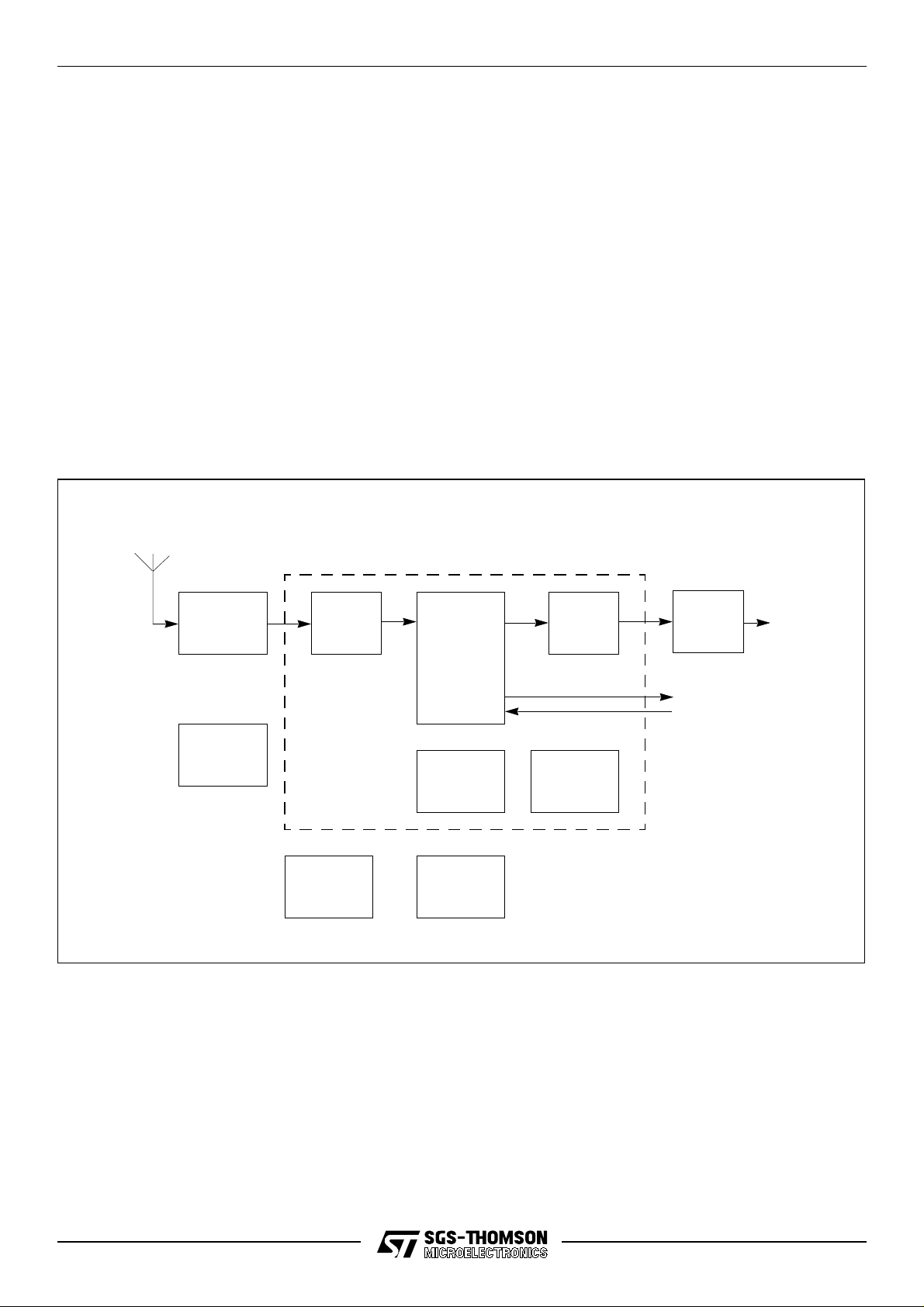
Antenna
Radio
Single chip
Low
cost
crystal
No TCXO
ST20-GP1
DSP
ASIC
CPU
Watchdog
timer
RAMROM
UART
Real
time
clock
Driver
(optional)
Parallel I/O
Figure 1.1 GPS system
The ST20-GP1 supports large values of frequency offset, allowing the use of a very low cost
oscillator, thus saving the cost of a Temperature Controlled Crystal Oscillator (TCXO).
The CPU and software have access to the part-processed signal to enable accelerated acquisition
time.
The ST20-GP1 can implement the GPS digital signal processing algorithms using less than 50% of
the available CPU processing power. This leaves the rest available for integrating OEM application
functions such as route-finding, map display and telemetry. A hardware microkernel in the ST20
5/116
Page 6

ST20-GP1
CPU supports the sharing of CPU time between applications without an operating system or
executive overhead.
The architecture is based on the ST20 CPU core and supporting macrocells developed by SGSTHOMSON Microelectronics. The ST20 micro-core family provides the tools and building blocks to
enable the development of highly integrated application specific 32-bit devices at the lowest cost
and fastest time to market. The ST20 macrocell library includes the ST20Cx family of 32-bit VLRISC (variable length reduced instruction set computer) micro-cores, embedded memories,
standard peripherals, I/O, controllers and ASICs.
The ST20-GP1 uses the ST20 macrocell library to provide the hardware modules required in a
GPS system. These include:
• DSP hardware
• Dual channel UART for serial communications
• 6 bits of parallel I/O
• Interrupt controller
• Real time clock/calendar
• Watchdog timer
The ST20-GP1 is supported by a range of software and hardware development tools for PC and
UNIX hosts including an ANSI-C ST20 software toolset and the ST20 INQUEST window based
debugging toolkit.
6/116
Page 7

ST20-GP1
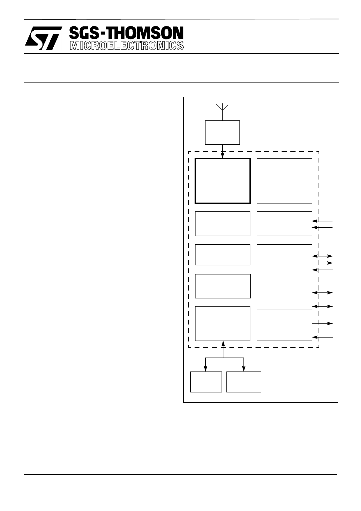
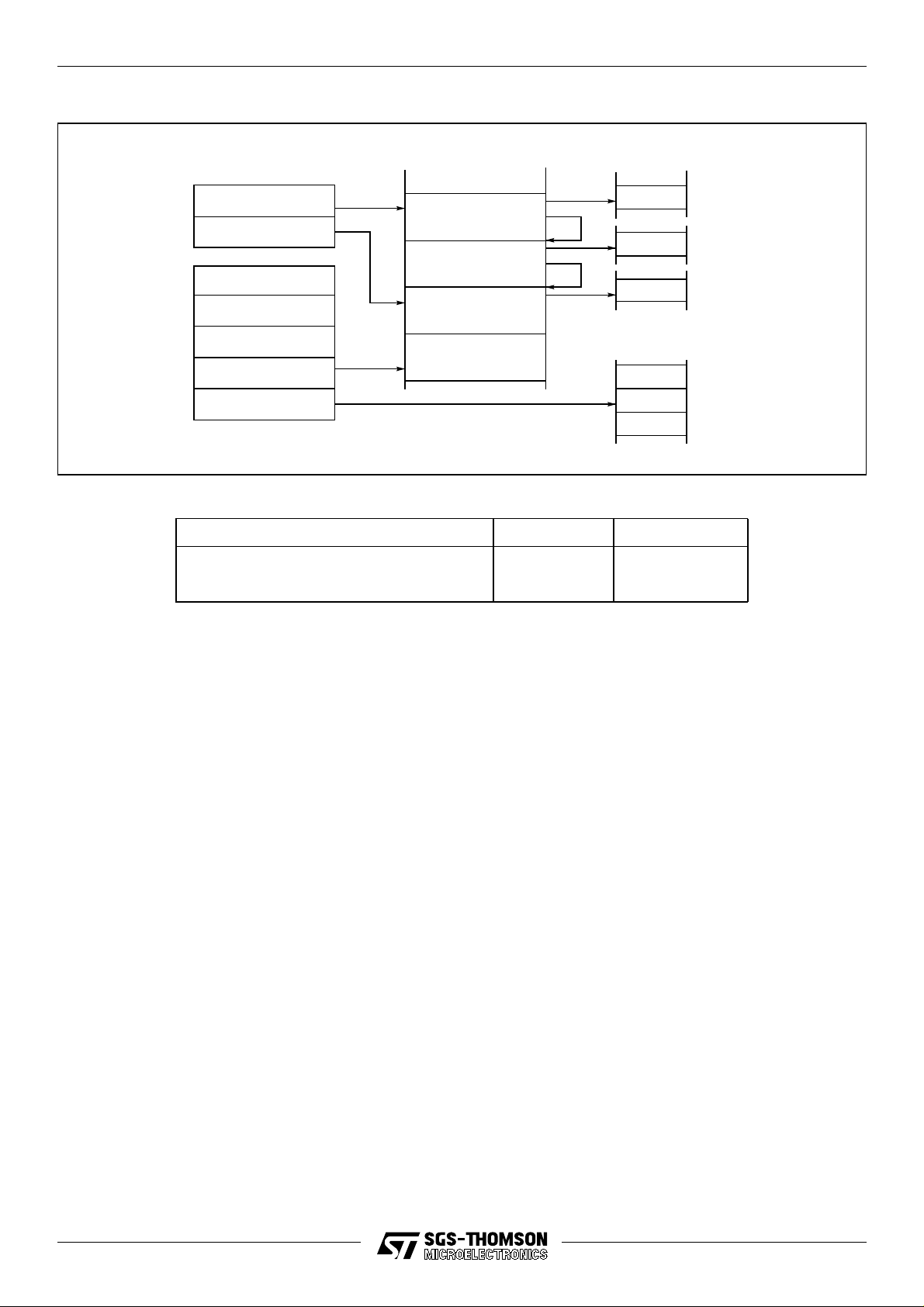
2 ST20-GP1 architecture overview
The ST20-GP1 consists of an ST20 CPU plus application specific DSP hardware for handling GPS
signals, plus a dual channel U AR T, 8-bit parallel half-duple x link interface, 6-bit parallel IO, real time
clock and watchdog functions.
Figure 2.1 shows the subsystem modules that comprise the ST20-GP1. These modules are
outlined below and more detailed information is given in the following chapters.
DSP
The ST20-GP1 includes DSP hardware for processing signals from the GPS satellites. The DSP
module generates the pseudo-random noise (prn) signals, and de-spreads the incoming signal.
It consists of a down conversion stage that takes the 4 MHz input signal down to nominally zero
frequency both in-phase and quadrature (I & Q). This is followed by 12 parallel hardware channels
for satellite tracking, whose output is passed to the CPU for further software processing at a
programmable interval, nominally every millisecond.
CPU
The Central Processing Unit (CPU) on the ST20-GP1 is the ST20 32-bit processor core. It contains
instruction processing logic, instruction and data pointers, and an operand register. It directly
accesses the high speed on-chip memory, which can store data or programs. The processor can
access up to 4 Mbytes of memory via the programmable memory interface.
7/116
Page 8
ST20-GP1
GPS
radio
ST20-GP1
Interrupts
12 channel GPS
hardware DSP
Interrupt
controller
Low
power
controller
Real time
clock
4K
SRAM
Programmable
memory
interface
ST20
CPU
Serial
communications
2 UART
1 OS-Link
Parallel
input/output
Byte-wide
parallel
port
System
services
.
.
6
.
.
.
8
.
OS-Link
Reset
Analyse
Error
Clock
User position
output in
ASCII
8/116
RAM
ROM/
FLASH
Figure 2.1 ST20-GP1 architectural block diagram
Page 9

ST20-GP1
Memory subsystem
The ST20-GP1 on-chip memory system provides 130 Mbytes/s internal data bandwidth,
supporting pipelined 2-cycle internal memory access at 30 ns cycle times. The ST20-GP1 memory
system consists of SRAM and a programmable memory interface. The programmable memory
interface is also referred to as an external memory interface (EMI).
The ST20-GP1 uses 8 or 16-bit external RAM, 8 or 16-bit ROM, and supports an address width of
20 bits.
The ST20-GP1 product has 4 Kbytes of on-chip SRAM. The advantage of this is the ability to store
time critical code on chip, for instance interrupt routines, software kernels or device drivers, and
even frequently used data.
The ST20-GP1 memory interface controls the movement of data between the ST20-GP1 and offchip memory. It is designed to support memory subsystems without any external support logic and
is programmable to support a wide range of memory types. Memory is divided into 4 banks which
can each have different memory characteristics and each bank can access up to 1 Mbyte of
external memory.
The normal memory provision in a simple GPS receiv er is a single 128K x 8-bit SRAM (55 or 70 ns
access time), and a single 64K x 16-bit ROM or Flash ROM (70, 90 or 100 ns access time). The
ST20-GP1 can support up to 1 Mbyte of SRAM plus 1 Mbyte of ROM, enabling additional
applications to be loaded if required.
Low power controller, real time clock and watchdog timer
The ST20-GP1 has power-down capabilities configurable in software. When powered down, a
timer can be used as an alarm, re-activating the CPU after a programmed dela y. This is suitable f or
ultra low power or solar powered applications such as container tracking, railway truck tracking, or
marine navigation buoys that must check they are on station at intervals. The timer can also be
used to provide a watchdog function, resetting the system if it times out.
The real time clock/calendar function is provided by a 64-bit binary counter running continuously
from the low-power clock (nominally 32768 Hz).
The ST20-GP1 is designed for 0.5 micron, 3.3 V CMOS technology and runs at speeds of up to
33 MHz. 3.3 V operation provides reduced power consumption internally and allows the use of low
power peripherals. In addition, a power-down mode is available on the ST20-GP1.
The different power levels of the ST20-GP1 are listed below.
• Operating power — power consumed during functional operation.
• Stand-by power — power consumed during little or no activity. The CPU is idle but ready to
immediately respond to an interrupt/reschedule.
• Power-down — clocks are stopped and power consumption is significantly reduced. Functional operation is stalled. Normal functional operation can be resumed from previous state
as soon as the clocks are stable. No information is lost during power down as all internal
logic is static.
• Power to most of the chip removed — only the real time clock supply (RTCVDD) power on.
In power-down mode the processor and all peripherals are stopped, including the e xternal memory
controller and optionally the PLL. Effectively the internal clock is stopped and functional operation
is stalled. On restart the clock is restarted and the chip resumes normal functional operation.
9/116
Page 10

ST20-GP1
Serial communications
The ST20-GP1 has two UARTs (Asynchronous Serial Controllers (ASCs)) for serial
communication. The UARTs provide an asynchronous serial interface and can be programmed to
support a range of baud rates and data formats, for example, data size, stop bits and parity.
There is one OS-Link on the ST20-GP1 which acts as a DMA engine independent of the CPU. The
OS-Link uses an asynchronous bit-serial (byte-stream) protocol, each bit received is sampled five
times, hence the term
oversampled link
(OS-Link). The OS-Link provides a pair of channels, one
input and one output channel. The link is used for:
• bootstrapping during development,
• debugging,
• communicating with OS-Link peripherals or other ST20 devices.
Interrupt subsystem
The ST20-GP1 interrupt subsystem supports five prioritized interrupts. Three interrupts are
connected to on-chip peripherals (2 for the UARTs, 1 for the programmable IO) and two are
available as external interrupt pins.
All interrupts are at a higher priority than the high priority process queue. Each interrupt lev el has a
higher priority than the previous and each level supports only one software handler process.
Note that interrupt handlers must not prevent the GPS DSP data tr affic from being handled. During
continuous operation this has 1 ms latency and is not a problem, but during initial acquisition it has
a 32 µs rate and thus all interrupts must be disabled except if used to stop GPS operation.
Byte-wide parallel port
The byte-wide parallel port is provided to communicate with an external device. It transfers a byte
at a time, operating half duplex in the program-selected direction.
Parallel IO module
Six bits of parallel IO are provided. Each bit is programmable as an output or an input. Edge
detection logic is provided which can generate an interrupt on any change of an input bit.
System services module
The ST20-GP1 system services module includes:
• reset, initialization and error port.
• phase locked loop (PLL) — accepts 16.368 MHz input and generates all the internal high
frequency clocks needed for the CPU and the OS-Link.
10/116
Page 11
ST20-GP1
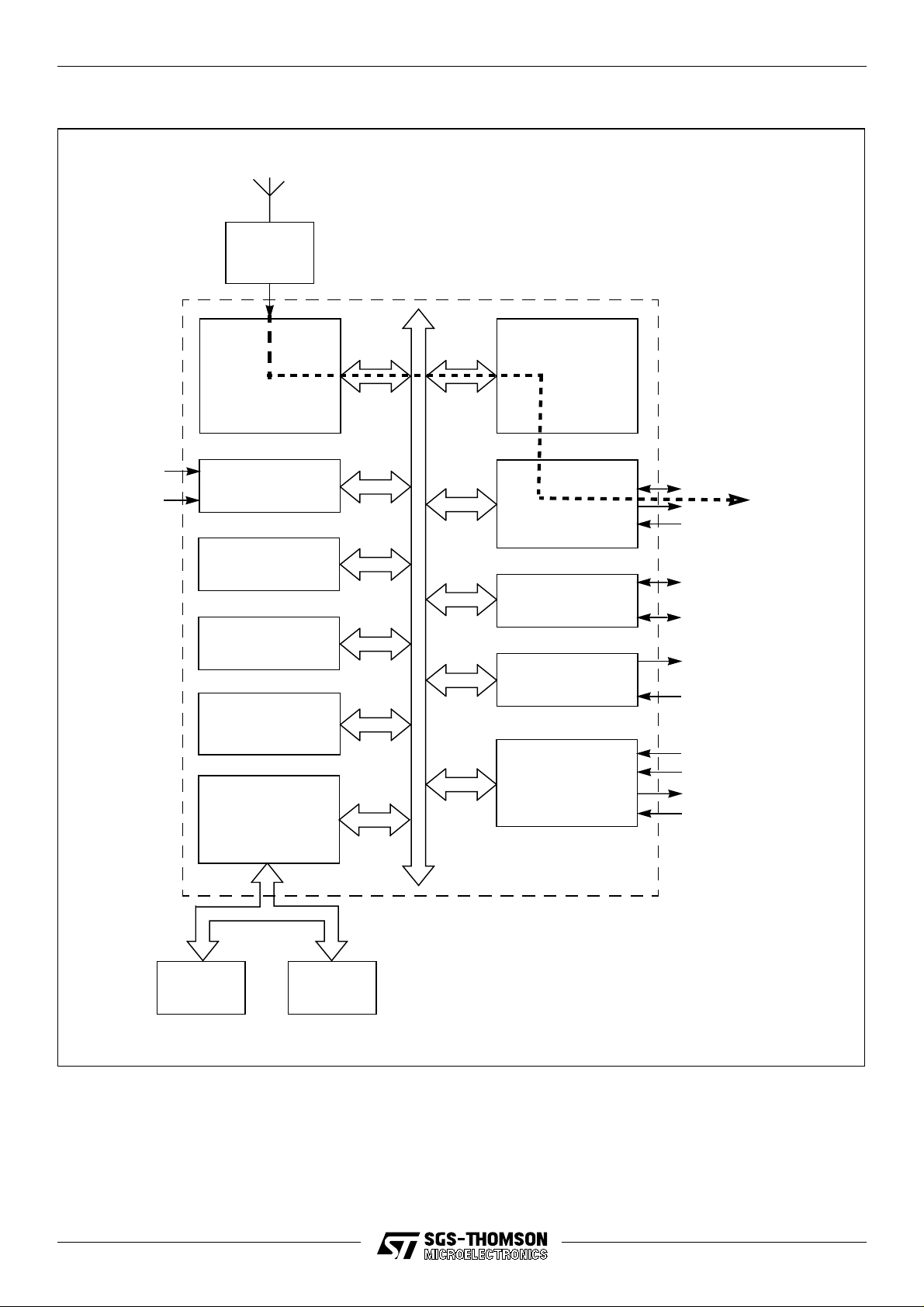
3 Digital signal processing module
The ST20-GP1 chip includes 12 channel GPS correlation DSP hardware. It is designed to handle
twelve satellites, two of which can be initialized to support the RTCA-SC159 specification.
The digital signal processing (DSP) module extracts GPS data from the incoming IF (Intermediate
Frequency) data. There are a number of stages of processing involved; these are summarized
below and in Figure 3.1. After the 12 pairs of hardware correlators, the data for all channels are
time division multiplexed onto the appropriate internal buses (i.e. values for each channel are
passed in sequence, for example: I
, Q1, I2, Q2 ... I12, Q12, I1, Q1).
1
4 MHz IF
input
data
sampler
frequency
converter A
Pseudo random
noise sequence
generator
(x 12)
ST20 CPU accessible
registers
I correlator
(x 12)
Q correlator
(x 12)
Numerically
controlled
oscillator
frequency
converter B
DMA
interface
accumulator
Figure 3.1 DSP module block diagram
The main stages of processing are as follows:
Data sampling
This stage removes any meta-stability caused by the asynchronous input data coming from an
analogue source (the radio receiver). The data at this point consists of a carrier of nominally
4.092 MHz with a bandwidth of approximately ±1 MHz.
This stage is common to all 12 channels.
Frequency conversion (A)
The first frequency converter mixes the sampled IF data with the (nominal) 4.092 MHz signal. This
is done twice with a quarter cycle offset to produce I and Q (In-phase and Quadrature) versions of
the data at nominal zero centre frequency (this can actually be up to ±132 KHz due to errors such
11/116
Page 12

ST20-GP1
as doppler shift, crystal accuracy, etc.). The sum frequency (~8 MHz) is removed by low-pass
filtering in the correlator.
This stage is common to all 12 channels.
Correlation against pseudo-random sequence
The GPS data is transmitted as a spread-spectrum signal (with a bandwidth of about 2 MHz). In
order to recover the data it is necessary to correlate against the same Pseudo-Random Noise
(PRN) signal that was used to transmit the data. The output of the correlator accumulator is
sampled at 264 KHz. The PRN sequences come from the PRN generator.
There is a correlator for the I and Q signals for each of the 12 channels. The output signal is now
narrowband.
Frequency conversion (B)
The second stage of frequency conversion mixes the data with the local oscillator signal generated
by the Numerically Controlled Oscillator (NCO). This signal is locked, under softw are control, to the
Space Vehicle (SV) frequency and phase to remove the errors and take the frequency and
bandwidth of the data down to 0 and ±50 Hz respectively. Filtering to 500 Hz is achieved in
hardware, to 50 Hz in software.
This stage is shared by time division multiplexing between all 12 channels. This is loss-free as the
stage supports 12 channels x 264 KHz, approximately 3 MHz, well within its 16 MHz clock rate.
Result integration
The final stage sums the I and Q values for each channel over a user defined period. In normal
operation, the sampling period is slightly less than the 1ms length of the PRN sequence. This
ensures that no data is lost, although it may mean that some data samples are seen twice — this is
handled (mainly) in software.
The sampling period can also be programmed to be much shorter (i.e. a higher cut-off frequency
for the filter) when the system is trying to find new satellites (‘acquisition mode’).
There are two further stages of buffering for the accumulated 16-bit I and Q values for each
1
channel. These allow for the slightly different time domains involved
.
The results after hardware processing of the signal, using the parameters set in the DSP registers,
refer to Section 3.1, are delivered to the CPU via a DMA engine in packet format. The CPU should
in
perform an
(input) instruction on the appropriate channel (see address map, Figure 7.1 on
page 47) in order to read a packet.
The format of the 62-byte packets is given in Figure 3.2. These represent a two byte header,
followed b y the 16-bit I-v alues for 12 channels, then the 16-bit Q-values for 12 channels, then the 8bit timestamp values for the 12 channels. The I and Q values are sent least significant byte first.
The 2 byte header contains: a ‘sync’ byte with the value #1B, and a ‘sample rate’ byte which
contains the two SampleRate bits from the DSPControl register, see Table 3.1.
Packets are delivered at the rate selected by the DSPControl register, even if new data is not
availab le . In this case, the data v alue f or the field is set to #8000. This guar antees that synchronism
1. Data sampled in SV time, data transmitted to the CPU at fixed intervals.
12/116
Page 13

ST20-GP1
is maintained between the satellite one-millisecond epochs and the receiver, despite time-ofreception variations due to the varying path length from the satellite.
62 byte packet every 840/970/31/62 µs
16-bit
header
sync
12 x 16-bit
I values
sample
rate
12 x 16-bit
Q values
Absent 16-bit values padded with #8000
Tracking mode
T[7:6] = 10
T[5:0] = time[5:0]
Figure 3.2 DSP packet format
12 x 8-bit
time values
Acquisition mode
First packet (in SV ms)
T[7:6] = 10
T[5:0] = time[5:0]
Remaining packets
T[7:6] = 00
T[5:0] = sequence number
(sequence numbers are 2 to
16 or 32)
3.1 DSP module registers
The GPS hardware channels of the ST20-GP1 are controlled by three sets of registers:
1 DSPControl register
2 PRNcode0-11 and PRNphase0-11 registers
3 NCOfrequency0-11 and NCOphase0-11 registers
The base addresses for the DSP registers are given in the Memory Map chapter.
DSPControl register
The DSPControl register determines whether the PRN generators are on (normal use) or disabled
(for built-in-self-test of a system), whether the system is in tracking mode (840/970 µs output rate)
or initial acquisition mode (31/62 µs), and selects which of the two rates for each mode. It also
determines whether the accumulated carrier phase in the NCO are reset to zero automatically or
continue from their existing value. The bit allocations are given in Table 3.1.
13/116
Page 14

ST20-GP1
DSPControl DSP base address + #140 Write only
Bit Bit field Function
1:0 SampleRate These bits control the sampling rate (the rate at which data is sent to the DMA
controller). The encoding of these bits is as follows:
SampleRate[1:0] Transfer period
00 840 µs 256 Tracking
01 970 µs 256
10 31 µs 8 Acquisition
11 62 µs16
2NCOResetEnable When set to 1, the accumulated NCO phase for a channel is reset when the corre-
sponding PRN code register is written.
3 PRNDisable When set to 1, all PRN generators are disabled.
No. of samples
accumulated
Mode
Table 3.1 DSPControl register format
PRNcode0-11 registers
The PRNcode0-11 registers choose the code for the particular satellite, and writing these causes a
reset to the accumulated carrier phase in the NCO for the corresponding channel, if enabled by the
DSPControl register.
PRNcode0-11 DSP base address + #00 to #2C Write only
Bit Bit field Function
6:0 PRNcode Satellite code as a 7-bit value.
Table 3.2 PRNcode0-11 register format
The bit-fields for selecting particular GPS satellites are given in Table 3.3.
Satellite ID
1 #62 6 2
2 #73 7 3
3 #04 8 4
4 #15 9 5
5 #11 9 1
6 #22 10 2
7 #01 8 1
8 #12 9 2
9 #23 10 3
10 #32 3 2
11 #43 4 3
12 #65 6 5
13 #76 7 6
14 #07 8 7
15 #18 9 8
PRNcode0-11
register value
Taps selected from G2 shift register
by bits 6 to 4 by bits 3 to 0
a
14/116
Table 3.3 PRNcode0-11 register value
Page 15

ST20-GP1
Satellite ID
16 #29 10 9
17 #41 4 1
18 #52 5 2
19 #63 6 3
20 #74 7 4
21 #05 8 5
22 #16 9 6
23 #31 3 1
24 #64 6 4
25 #75 7 5
26 #06 8 6
27 #17 9 7
28 #28 10 8
29 #61 6 1
30 #72 7 2
31 #03 8 3
32 #14 9 4
- #25 10 5
- #24 10 4
- #71 7 1
- #02 8 2
- #24 10 4
b
WAAS
PRNcode0-11
register value
#20 10 0
Taps selected from G2 shift register
by bits 6 to 4 by bits 3 to 0
a
Table 3.3 PRNcode0-11 register value
a. Refer to the US DoD document ICD-GPS-200.
b. It is the responsibility of the software to ensure that when this value is selected, a suitable value has
been written into the PRNinitialVal0-1 register. If this channel is later used for a standard GPS satellite, the PRNinitialVal0-1 must be set to all ones (#3FF).
For channels 0 and 1, RTCA-SC159 satellite codes can also be selected. This is achieved by
setting the PRNcode0-11 register appropriately and also writing the initial value for the satellite to
the PRNinitialVal0-1 register, see Table 3.8. If uninitialized by the software, the PRNinitialVal
register defaults to 11 1111 1111 (#3FF) as required for GPS satellites.
The PRNcode0-11 and PRNinitialVal0-1 registers are normally written only when the satellite is
first chosen.
PRNphase0-11 registers
The PRN0-11phase registers determine the relative delay between the receiver master clock, and
the start of the one millisecond repetitive code sequence. The code sequence starts when the
receiver clock counter (invisible to the software except through message timestamps) reaches the
value written to the PRNphase0-11 register. The PRNphase0-11 register must only be written
once per satellite milliseconds-epoch, which varies from the receiver epoch dynamically due to
satellite motion. Synchronism with the software is achieved by reading the register, when a wr ite
enable flag is returned. If not enabled, the write operation is abandoned by the software.
15/116
Page 16

ST20-GP1
The 19-bit value comprises three fields. The 3 least significant bits represent the fractional-delay in
eighths of a code-chip. The middle 10 bits represent the integer delay in code-chips, 0-1022, with
the value 1023 illegal. The upper 6 most significant bits represent the dela y in integer milliseconds.
PRNphase0-11 DSP base address + #40 to #6C Write only
Bit Bit field Function
2:0 FractionalDelay Fractional delay in eighths of a code-chip.
12:3 IntegerDelay Integer delay in code-chips. Value 0-1022. Note, the value 1023 is illegal.
18:13 Delay Delay in integer milliseconds.
Table 3.4 PRNphase0-11 register format
Note also that the eighth-chip resolution of the code generator is not sufficient for positioning. At
125 ns it represents approximately 40 m of range, over 100 m of position. The software must
maintain the range measurements around the 1 ns resolution level in a 32-bit field, and send an
appropriate 19-bit sub-field to the register. Note, care m ust be taken when calculating this field from
a computed delay, or vice versa, to allow for the missing value 1023. The overall register bit-field
cannot be used mathematically as a single binary number.
PRNphase0-11WrEn registers
The PRNphase0-11WrEn flags are active low flags that record when the PRNphase0-11 register
can be updated. The PRNphaseWrEn flag for a channel is set high when the corresponding
PRNphase register is written. The flag is reset again when the value written is loaded into the PRN
generator. Note, the PRNphase0-11 register should only be updated when the PRNphase0-
11WrEn register has been cleared by the hardware.
PRNphase0-11WrEn DSP base address + #40 to #6C Read only
Bit Bit field Function
0 PRNphaseWrEn Set when the corresponding PRNphase0-11 register is set.
Table 3.5 PRNphase0-11WrEn register format
NCOfrequency0-11 registers
The NCOfrequency0-11 registers hold a signed 18-bit value that is added repetitively, ignoring
overflows, to the accumulated NCO phase from which the NCO sine and cosine waveforms are
generated. The addition is performed at a 264 KHz rate (16.368MHz/62). The accumulated NCO
phase is not accessible to the software, but can be cleared when initialising the channel if enabled
by the DSPControl register.
18
Each unit value in the NCOfrequency0-11 register represents 264KHz/(2
), i.e.
1.007080078125 Hz.
If the extreme values are written, #1FFFF and #20000, the sine wave generated will be at
approximately +132 KHz, and precisely -132 KHz respectively.
NCOfrequency0-11 DSP base address + #80 to #AC Write only
Bit Bit field Function
17:0 NCOfrequency NCO frequency as a signed 18-bit value.
Table 3.6 NCOfrequency0-11 register format
16/116
Page 17

ST20-GP1
NCOphase0-11 registers
The NCOphase0-11 registers contents are added to the accumulated phase to correct the carrier
for the final 1 Hz that cannot be resolved by the NCO frequency. This addition is not cumulative,
and the value must be updated regularly by the software as a result of carrier phase errors
measured on the satellite signal. The register holds a signed 7-bit field representing +/-180
degrees total in steps of 2.8125 degrees (360/128).
NCOphase0-11 DSP base address + #C4 to #EC Write only
Bit Bit field Function
6:0 NCOphase NCO phase as a signed 7-bit value representing +/-180 degrees total in steps of
2.8125 degrees (360/128).
Table 3.7 NCOphase0-11 register format
PRNinitialVal0-1 registers
The initial value for the two RTCA-SC159 capable satellites channels should be written to the
PRNinitialVal0-1 registers. The value can be found in the
RTCA-SC159 Specification
.
Note: The value written to the register is the Initial Value defined by RTCA-SC159 for the PRN
required. The conversion from ‘big-endian’ as used in the specification to ‘little-endian’ as
conventionally used in ST20 architectures has been implemented in the hardware.
If uninitialized by the software, this register defaults to 11 1111 1111 (#3FF) as required for GPS
satellites.
PRNinitialVal0-1 DSP base address + #100, #104 Write only
Bit Bit field Function
9:0 InitialValue Initial value of the RTCA-SC159 satellite channel.
Table 3.8 PRNinitialVal0-1 register format
17/116
Page 18

ST20-GP1
4 Central processing unit
The Central Processing Unit (CPU) is the ST20 32-bit processor core. It contains instruction
processing logic, instruction and data pointers, and an operand register. It can directly access the
high speed on-chip memory, which can store data or programs. Where larger amounts of memory
are required, the processor can access memory via the External Memory Interface (EMI).
The processor provides high performance:
• Fast integer multiply — 3 cycle multiply
• Fast bit shift — single cycle barrel shifter
• Byte and part-word handling
• Scheduling and interrupt support
• 64-bit integer arithmetic support
The scheduler provides a single level of pre-emption. In addition, multi-level pre-emption is
provided by the interrupt subsystem, see Chapter 5 for details. Additionally, there is a per-priority
trap handler to improve the support for arithmetic errors and illegal instructions, ref er to section 4.6.
4.1 Registers
The CPU contains six registers which are used in the execution of a sequential integer process.
The six registers are:
• The workspace pointer (Wptr) which points to an area of store where local data is kept.
• The instruction pointer (IptrReg) which points to the next instruction to be executed.
• The status register (StatusReg).
• The Areg, Breg and Creg registers which form an evaluation stack.
The Areg, Breg and Creg registers are the sources and destinations for most arithmetic and
logical operations. Loading a value into the stack pushes Breg into Creg, and Areg into Breg,
before loading Areg. Storing a value from Areg, pops Breg into Areg and Creg into Breg. Creg is
left undefined.
Local data ProgramRegisters
Areg
Breg
Creg
18/116
Wptr
IptrReg
Figure 4.1 Registers used in sequential integer processes
Page 19

ST20-GP1
Expressions are evaluated on the evaluation stack, and instructions refer to the stack implicitly. For
add
example, the
instruction adds the top two values in the stack and places the result on the top of
the stack. The use of a stack removes the need for instructions to explicitly specify the location of
their operands. No hardware mechanism is provided to detect that more than three values have
been loaded onto the stack; it is easy for the compiler to ensure that this never happens.
Note that a location in memory can be accessed relative to the workspace pointer, enabling the
workspace to be of any size.
The use of shadow registers provides fast, simple and clean context switching.
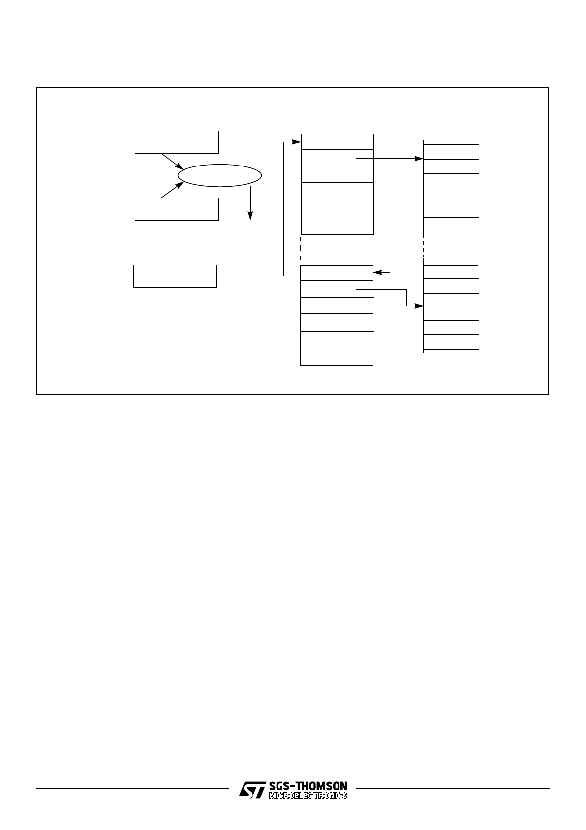
4.2 Processes and concurrency
The following section describes ‘default’ behavior of the CPU and it should be noted that the user
can alter this behavior, for example, by disabling timeslicing, installing a user scheduler, etc.
A process starts, performs a number of actions, and then either stops without completing or
terminates complete. Typically, a process is a sequence of instr uctions. The CPU can run several
processes in parallel (concurrently). Processes may be assigned either high or low priority, and
there may be any number of each.
The processor has a microcoded scheduler which enables any number of concurrent processes to
be executed together, sharing the processor time. This removes the need for a software kernel,
although kernels can still be written if desired.
At any time, a process may be
active
- being executed
- interrupted by a higher priority process
- on a list waiting to be executed
inactive
- waiting to input
- waiting to output
- waiting until a specified time
The scheduler operates in such a way that inactive processes do not consume any processor time.
Each active high priority process executes until it becomes inactive. The scheduler allocates a
portion of the processor’s time to each active low priority process in turn (see Section 4.3). Active
processes waiting to be executed are held in two linked lists of process workspaces, one of high
priority processes and one of low priority processes. Each list is implemented using two registers,
one of which points to the first process in the list, the other to the last. In the linked process list
S
shown in Figure 4.2, process
is ex ecuting andP,Q andR are active, a w aiting e xecution. Only the
low priority process queue registers are shown; the high priority process ones behave in a similar
manner.
19/116
Page 20
ST20-GP1
Registers Program
FptrReg1
BptrReg1
Areg
Breg
Creg
Wptr
IptrReg
Local Data
pw.Iptr
P
pw.Link
pw.Iptr
Q
pw.Link
pw.Iptr
R
S
Figure 4.2 Linked process list
Function High priority Low priority
Pointer to front of active process list FptrReg0 FptrReg1
Pointer to back of active process list BptrReg0 BptrReg1
Table 4.1 Priority queue control registers
Each process runs until it has completed its action or is descheduled. In order for several
processes to operate in parallel, a low priority process is only permitted to execute for a maximum
of two timeslice periods. After this, the machine deschedules the current process at the next
timeslicing point, adds it to the end of the low priority scheduling list and instead executes the next
active process. The timeslice period is 1ms.
There are only certain instructions at which a process may be descheduled. These are known as
descheduling points. A process may only be timesliced at certain descheduling points. These are
known as timeslicing points and are defined in such a way that the operand stack is always empty.
This removes the need for saving the operand stack when timeslicing. As a result, an expression
evaluation can be guaranteed to execute without the process being timesliced part way through.
Whenever a process is unable to proceed, its instruction pointer is saved in the process w orkspace
and the next process taken from the list.
The processor core provides a number of special instructions to support the process model,
including
construct,
startp
(start process) and
startp
is used to create the necessary additional concurrent processes. A
endp
(end process). When a main process executes a parallel
startp
instruction creates a new process by adding a new workspace to the end of the scheduling list,
enabling the new concurrent process to be executed together with the ones already being
executed. When a process is made active it is always added to the end of the list, and thus cannot
pre-empt processes already on the same list.
endp
The correct termination of a parallel construct is assured by use of the
instruction. This uses
a data structure that includes a counter of the parallel construct components which have still to
terminate. The counter is initialized to the number of components before the processes are started.
endp
Each component ends with an
20/116
instruction which decrements and tests the counter. F or all but
Page 21

ST20-GP1
the last component, the counter is non zero and the component is descheduled. For the last
component, the counter is zero and the main process continues.
4.3 Priority
The following section describes ‘default’ behavior of the CPU and it should be noted that the user
can alter this behavior, for example, by disabling timeslicing and priority interrupts.
The processor can execute processes at one of two priority levels, one level for urgent (high
priority) processes, one for less urgent (low priority) processes. A high priority process will always
execute in preference to a low priority process if both are able to do so.
High priority processes are expected to execute for a short time. If one or more high priority
processes are active, then the first on the queue is selected and executes until it has to wait for a
communication, a timer input, or until it completes processing.
If no process at high priority is active, but one or more processes at low priority are active , then one
is selected. Low priority processes are periodically timesliced to provide an even distribution of
processor time between computationally intensive tasks.
n
If there are
process becomes active to the time when it starts processing is the order of 2
is then able to execute for between one and two timeslice periods, less any time taken by high
priority processes. This assumes that no process monopolizes the CPU’s time; i.e. it has frequent
timeslicing points.
low priority processes, then the maximum latency from the time at which a low priority
n
timeslice periods. It
The specific condition for a high priority process to start execution is that the CPU is idle or running
at low priority and the high priority queue is non-empty.
If a high priority process becomes able to run whilst a low priority process is executing, the low
priority process is temporarily stopped and the high prior ity process is executed. The state of the
low priority process is saved into ‘shadow’ registers and the high priority process is executed.
When no further high priority processes are able to run, the state of the interrupted low priority
process is re-loaded from the shadow registers and the interrupted low priority process continues
executing. Instructions are provided on the processor core to allow a high priority process to store
the shadow registers to memory and to load them from memory. Instructions are also provided to
allow a process to exchange an alternative process queue for either priority process queue (see
Table 6.21 on page 43). These instructions allow extensions to be made to the scheduler for
custom runtime kernels.
A low priority process may be interrupted after it has completed execution of any instruction. In
addition, to minimize the time taken for an interrupting high priority process to star t executing, the
potentially time consuming instructions are interruptible. Also some instructions are abortable and
are restarted when the process next becomes active (refer to the Instruction Set chapter).
4.4 Process communications
Communication between processes takes place over channels, and is implemented in hardware.
Communication is point-to-point, synchronized and unbuffered. As a result, a channel needs no
process queue, no message queue and no message buffer.
A channel between two processes executing on the same CPU is implemented by a single word in
memory; a channel between processes executing on different processors is implemented by point-
21/116
Page 22

ST20-GP1
to-point links. The processor provides a number of operations to support message passing, the
most important being
in
and
out
The
instructions use the address of the channel to determine whether the channel is
(input message) and
out
(output message).
in
internal or external. This means that the same instruction sequence can be used for both hard and
soft channels, allowing a process to be written and compiled without knowledge of where its
channels are implemented.
Communication takes place when both the inputting and outputting processes are ready.
Consequently, the process which first becomes ready must wait until the second one is also ready.
The inputting and outputting processes only become active when the communication has
completed.
A process performs an input or output by loading the e valuation stack with, a pointer to a message,
the address of a channel, and a count of the number of bytes to be transferred, and then executing
in
or
out
an
instruction.
4.5 Timers
There are two 32-bit hardware timer clocks which ‘tick’ periodically. These are independent of any
on-chip peripheral real time clock. The timers provide accurate process timing, allowing processes
to deschedule themselves until a specific time.
One timer is accessible only to high priority processes and is incremented every microsecond,
cycling completely in approximately 4295 seconds. The other is accessible only to low priority
processes and is incremented every 64 microseconds, giving 15625 ticks in one second. It has a
full period of approximately 76 hours. All times are approximate due to the clock rate.
Register Function
ClockReg0 Current value of high priority (level 0) process clock
ClockReg1 Current value of low priority (level 1) process clock
TnextReg0 Indicates time of earliest event on high priority (level 0) timer queue
TnextReg1 Indicates time of earliest event on low priority (level 1) timer queue
TptrReg0 High priority timer queue
TptrReg1 Low priority timer queue
Table 4.2 Timer registers
The current value of the processor clock can be read b y executing a
tin
A process can arrange to perform a
after a specified time has been reached. The
(timer input), in which case it will become ready to execute
tin
instruction requires a time to be specified. If this
ldtimer
(load timer) instruction.
time is in the ‘past’ then the instruction has no effect. If the time is in the ‘future’ then the process is
descheduled. When the specified time is reached the process becomes active. In addition, the
ldclock
clockenb
(load clock),
(clock enable),
stclock
(store clock) instructions allow total control ov er the cloc k v alue and the
clockdis
(clock disable) instructions allow each clock to be individually
stopped and re-started.
Figure 4.3 shows two processes waiting on the timer queue, one waiting for time 21, the other for
time 31.
Note, these timers stop counting when power-down mode (see Section 10.2 on page 61) is
invoked.
22/116
Page 23
ClockReg0
ST20-GP1
Workspaces
Program
5
comparator
TnextReg0
TptrReg0
21
Alarm
21
Empty
31
Figure 4.3 Timer registers
4.6 Traps and exceptions
A software error, such as arithmetic overflow or array bounds violation, can cause an error flag to
be set in the CPU. The flag is directly connected to the ErrorOut pin. Both the flag and the pin can
be ignored, or the CPU stopped. Stopping the CPU on an error means that the error cannot cause
further corruption. As well as containing the error in this way it is possible to determine the state of
the CPU and its memory at the time the error occurred. This is par ticularly useful for postmortem
debugging where the debugger can be used to examine the state and history of the processor
leading up to and causing the error condition.
In addition, if a trap handler process is installed, a variety of traps/exceptions can be trapped and
handled by software. A user supplied trap handler routine can be provided for each high/low
process priority level. The handler is started when a trap occurs and is given the reason for the
trap. The trap handler is not re-entrant and must not cause a trap itself within the same group. All
traps are individually maskable.
4.6.1 Trap groups
The trap mechanism is arranged on a per priority basis. For each priority there is a handler for each
group of traps, as shown in Figure 4.4.
23/116
Page 24

ST20-GP1
Low priority traps High priority traps
Scheduler
trap handler
Breakpoint
trap handler
CPU Error
trap handler
System operations
trap handler
Figure 4.4 Trap arrangement
There are four groups of traps, as detailed below.
• Breakpoint
This group consists of the
Breakpoint
trap. The breakpoint instruction (j0) calls the break-
point routine via the trap mechanism.
• Errors
The traps in this group are
IntegerError
and
flow, such as arithmetic results which do not fit in the result word.
errors caused when data is erroneous, for example when a range checking instruction finds
that data is out of range.
• System operations
This group consists of the
LoadTrap,StoreTrap
trap is signalled when an attempt is made to execute an illegal instruction. The
and
StoreTrap
traps allow a kernel to intercept attempts by a monitored process to change
or examine trap handlers or trapped process infor mation. It enables a user program to signal to a kernel that it wishes to install a new trap handler.
CPU Error
trap handler
Breakpoint
trap handler
Overflow.Overflow
and
IllegalOpcode
Scheduler
trap handler
System operations
trap handler
represents arithmetic over-
IntegerError
traps. The
represents
IllegalOpcode
LoadTrap
• Scheduler
The scheduler trap group consists of the
lice, Run, Signal, ProcessInterrupt
nals that the machine has performed a priority interrupt from low to high. The
trap indicates that there is no further executable work to perform. The other traps in this
group indicate that the hardware scheduler wants to schedule a process on a process
queue, with the different traps enabling the different sources of this to be monitored.
The scheduler traps enable a software scheduler kernel to use the hardware scheduler to
implement a multi-priority software scheduler.
Note that scheduler traps are different from other traps as they are caused by the microscheduler rather than by an executing process.
Note, when the scheduler trap is caused by a process that is ready to be scheduled, the
Wptr of that process is stored in the workspace of the scheduler trap handler, at address 0.
The trap handler can access this using a
24/116
ExternalChannel, InternalChannel, Timer, TimeS-
and
QueueEmpty
ldl 0
traps. The
instruction.
ProcessInterrupt
QueueEmpty
trap sig-
Page 25

ST20-GP1
Trap groups encoding is shown in Table 4.4 below. These codes are used to identify trap groups to
various instructions.
Trap group Code
Breakpoint 0
CPU Errors 1
System operations 2
Scheduler 3
Table 4.3 Trap group codes
In addition to the trap groups mentioned above, the CauseError flag in the Status register is used
to signal when a trap condition has been activated by the
causeerror
instruction. It can be used to
indicate when trap conditions have occurred due to the user setting them, rather than by the
system.
4.6.2 Events that can cause traps
Table 4.4 summarizes the events that can cause traps and gives the encoding of bits in the trap
Status and Enable words.
Trap cause Status/Enable
codes
Breakpoint
IntegerError
Overflow
IllegalOpcode
LoadTrap
StoreTrap
InternalChannel
ExternalChannel
Timer
Timeslice
Run
0 0 When a process executes the breakpoint instruction (j0) then it traps
1 1 Integer error other than integer overflow – e.g. explicitly checked or
2 1 Integer overflow or integer division by zero.
3 2 Attempt to execute an illegal instruction. This is signalled when
4 2 When the trap descriptor is read with the
5 2 When the trap descriptor is written with the
6 3 Scheduler trap from internal channel.
7 3 Scheduler trap from external channel.
8 3 Scheduler trap from timer alarm.
9 3 Scheduler trap from timeslice.
10 3 Scheduler trap from
Trap
group
Comments
to its trap handler.
explicitly set error.
opr
(operate) is executed with an invalid operand.
ldtraph
instruction or when the trapped process status is read with the
ldtrapped
instruction or when the trapped process status is written with the
sttrapped
(load trapped) instruction.
(store trapped) instruction.
runp
(run process) or
sttraph
(load trap handler)
(store trap handler)
startp
(start process).
Signal
ProcessInterrupt
QueueEmpty
CauseError
11 3 Scheduler trap from
12 3 Start executing a process at a new priority level.
13 3 Caused by no process active at a priority level.
15 (Status only) Any ,
encoded
0-3
Signals that the
signal
causeerror
.
instruction set the trap flag.
Table 4.4 Trap causes and Status/Enable codes
25/116
Page 26

ST20-GP1
4.6.3 Trap handlers
For each trap handler there is a trap handler structure and a trapped process structure. Both the
trap handler structure and the trapped process structure are in memory and can be accessed via
instructions, see Section 4.6.4.
The trap handler structure specifies what should happen when a trap condition is present, see
Table 4.6.
Comments
Iptr Iptr of trap handler process. Base + 3
Wptr Wptr of trap handler process. Base + 2
Status Contains the Status register that the trap handler starts with. Base + 1
Enables Contains a word which encodes the trap enable and global interrupt masks which will be
ANDed with the existing masks to allow the trap handler to disable various events while it
runs.
Base + 0
Table 4.5 Trap handler structure
The trapped process structure saves some of the state of the process that was running when the
trap was taken, see Table 4.7.
Comments
Iptr Points to the instruction after the one that caused the trap condition. Base + 3
Wptr Wptr of the process that was running when the trap was taken. Base + 2
Status The relevant trap bit is set, see Table 4.5 for trap codes. Base + 1
Enables Interrupt enables. Base + 0
Table 4.6 Trapped process structure
In addition, for each priority, there is an Enables register and a Status register. The Enables
register contains flags to enable each cause of trap. The Status register contains flags to indicate
which trap conditions have been detected. The Enables and Status register bit encodings are
given in Table 4.4.
A trap will be taken at an interruptible point if a trap is set and the corresponding trap enable bit is
set in the Enables register. If the trap is not enabled then nothing is done with the trap condition. If
the trap is enabled then the corresponding bit is set in the Status register to indicate the trap
condition has occurred.
When a process takes a trap the processor saves the existing Iptr, Wptr, Status and Enables in
the trapped process structure. It then loads Iptr, Wptr and Status from the equivalent trap handler
structure and ANDs the value in Enables with the value in the structure. This allows the user to
disable various events while in the handler, in particular a trap handler must disable all the traps of
its trap group to avoid the possibility of a handler trapping to itself.
The trap handler then executes. The values in the trapped process structure can be examined
using the
ldtrapped
operation it returns to the trapped process via the
instruction (see Section 4.6.4). When the trap handler has completed its
tret
(trap return) instruction. This reloads the
values saved in the trapped process structure and clears the trap flag in Status.
Note that when a trap handler is started, Areg, Breg and Creg are not saved. The trap handler
stl
must save the Areg, Breg, Creg registers using
26/116
(store local).
Page 27

4.6.4 Trap instructions
ST20-GP1
Trap handlers and trapped processes can be set up and examined via the
ldtrapped
and
sttrapped
instructions. Table 4.8 describes the instructions that may be used when
ldtraph,sttraph
dealing with traps.
Instruction Meaning Use
ldtraph
sttraph
ldtrapped
sttrapped
trapenb
trapdis
tret
causeerror
load trap handler load the trap handler from memory to the trap handler descriptor
store trap handler store an existing trap handler descriptor to memory
load trapped load replacement trapped process status from memory
store trapped store trapped process status to memory
trap enable enable traps
trap disable disable traps
trap return used to return from a trap handler
cause error program can simulate the occurrence of an error
Table 4.7 Instructions which may be used when dealing with traps
The first four instructions transfer data to/from the trap handler structures or trapped process
structures from/to an area in memory. In these instructions Areg contains the trap group code (see
Table 4.4) and Breg points to the 4 word area of memor y used as the source or destination of the
transfer. In addition Creg contains the priority of the handler to be installed/examined in the case of
ldtraphor sttraph. ldtrapped
and
sttrapped
apply only to the current priority.
,
If the
LoadTrap
LoadTrap trap flag. If the
trap is enabled then
StoreTrap
ldtraph
and
ldtrapped
trap is enabled then
do not perform the transfer but set the
sttraph
and
sttrapped
do not perform the
transfer but set the StoreTrap trap flag.
The trap enable masks are encoded by an array of bits (see Table 4.5) which are set to indicate
which traps are enabled. This array of bits is stored in the lower half-word of the Enables register.
There is an Enables register for each priority. Traps are enabled or disabled by loading a mask into
Areg with bits set to indicate which traps are to be affected and the priority to affect in Breg.
Executing
trapenb
register for the priority in Breg. Executing
ORs the mask supplied in Areg with the trap enables mask in the Enables
trapdis
negates the mask supplied in Areg and ANDs it
with the trap enables mask in the Enables register for the priority in Breg. Both instructions return
the previous value of the trap enables mask in Areg.
4.6.5 Restrictions on trap handlers
There are various restrictions that must be placed on trap handlers to ensure that they work
correctly.
1 Trap handlers must not deschedule or timeslice. Trap handlers alter the Enables masks,
therefore they must not allow other processes to execute until they have completed.
2 Trap handlers must have their Enable masks set to mask all traps in their trap group to
avoid the possibility of a trap handler trapping to itself.
3 Trap handlers must terminate via the
is that a scheduler kernel may use
restart
tret
(trap return) instruction.The only exception to this
to return to a previously shadowed process.
27/116
Page 28
ST20-GP1
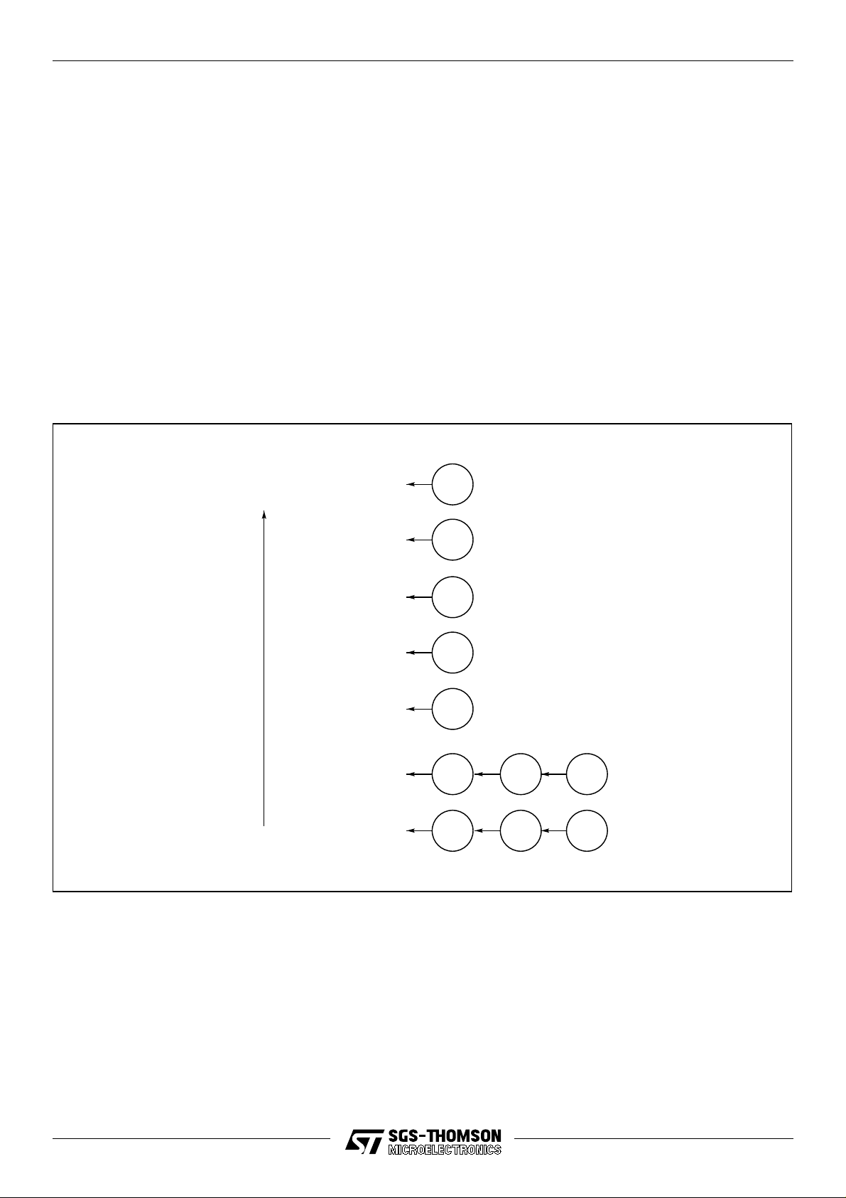
5 Interrupt controller
The ST20-GP1 supports external interrupts, enabling an on-chip subsystem or external interrupt
pin to interrupt the currently running process in order to run an interrupt handling process.
The ST20-GP1 interrupt subsystem supports five prioritized interrupts. This allows nested preemptive interrupts for real-time system design. Three interrupts are connected to on-chip
peripherals (2 for the UARTs, 1 for the programmable IO) and two are available as external
interrupt pins.
All interrupts are at a higher priority than the high priority process queue, see Figure 5.1. Each
interrupt level has a higher priority than the previous (interrupt 0 is lowest priority) and each level
supports only one software handler process.Note that interrupt handlers must not prevent the GPS
DSP data traffic from being handled. During continuous operation this has 1 ms latency and is not
a problem, but during initial acquisition it has a 32 µs rate and thus all interrupts must be disabled
except if used to stop GPS operation.
Increasing
pre-emption
Interrupt 4
Interrupt1 pin
Interrupt 3
Interrupt0 pin
Interrupt 2
UART1
Interrupt 1
UART0
Interrupt 0
Programmable IO
High priority
process
Low priority
process
Figure 5.1 Interrupt priority
Interrupts on the ST20-GP1 are implemented via an on-chip interrupt controller peripheral. An
interrupt can be signalled to the controller by one of the following:
• a signal on an external Interrupt pin
• a signal from an internal peripheral or subsystem
• software asserting an interrupt in a bit mask
28/116
Page 29

ST20-GP1
5.1 Interrupt vector table
The interrupt controller contains a table of pointers to interrupt handlers. Each interrupt handler is
represented by its workspace pointer (Wptr). The table contains a workspace pointer f or each level
of interrupt.
The Wptr gives access to the code, data and interrupt save space of the interrupt handler. The
position of the Wptr in the interrupt table implies the priority of the interrupt.
Run-time library support is provided for setting and programming the vector table.
5.2 Interrupt handlers
At any interruptible point in its execution the CPU can receive an interrupt request from the
interrupt controller. The CPU immediately acknowledges the request.
In response to receiving an interrupt the CPU performs a procedure call to the process in the
vector table . The state of the interrupted process is stored in the workspace of the interrupt handler
as shown in Figure 5.2. Each interrupt level has its own workspace.
Wptr
Before interrupt
Handler Iptr
Handler Status
Wptr
Interrupting high priority
process
Handler Iptr
Handler Status
Creg
Breg
Areg
Iptr
Wptr
Status
Interrupting low priority
process or CPU idle
Wptr
Handler Iptr
Handler Status
Null Status
Figure 5.2 State of interrupted process
The interrupt routine is initialized with space below Wptr. The Iptr and Status word for the routine
are stored there permanently . This should be prog rammed bef ore theWptr is written into the vector
table. The behavior of the interrupt differs depending on the priority of the CPU when the interrupt
occurs.
When an interrupt occurs when the CPU was running at high priority, the CPU saves the current
process state (Areg, Breg, Creg, Wptr, Iptr and Status) into the workspace of the interrupt
handler. The value HandlerWptr, which is stored in the interrupt controller, points to the top of this
29/116
Page 30

ST20-GP1
workspace. The values of Iptr and Status to be used by the interrupt handler are loaded from this
workspace and starts executing the handler. The value of Wptr is then set to the bottom of this
save area.
When an interrupt occurs when the CPU was idle or running at low priority, the Status is saved.
This indicates that no valid process is running (
Null Status
process) state is stored in shadow registers. This state can be accessed via the
shadow registers) and
stshadow
(store shadow registers) instructions. The interrupt handler is then
). The interrupted processes (low priority
ldshadow
(load
run at high priority.
When the interrupt routine has completed it must adjust Wptr to the value at the start of the
iret
handler code and then execute the
(interrupt return) instruction. This restores the interr upted
state from the interrupt handler structure and signals to the interrupt controller that the interrupt has
completed. The processor will then continue from where it was before being interrupted.
5.3 Interrupt latency
The interrupt latency is dependent on the data being accessed and the position of the interrupt
handler and the interrupted process. This allows systems to be designed with the best trade-off use
of fast internal memory and interrupt latency.
5.4 Pre-emption and interrupt priority
Each interrupt channel has an implied priority fixed by its place in the interrupt vector table. All
interrupts will cause scheduled processes of any priority to be suspended and the interrupt handler
started. Once an interrupt has been sent from the controller to the CPU the controller keeps a
record of the current executing interrupt priority. This is only cleared when the interrupt handler
iret
executes a return from interrupt (
) instruction. Interrupts of a lower priority arriving will be
blocked by the interrupt controller until the interrupt priority has descended to such a level that the
routine will execute. An interrupt of a higher priority than the currently executing handler will be
passed to the CPU and cause the current handler to be suspended until the higher priority interrupt
is serviced.
In this way interrupts can be nested and a higher priority interrupt will always pre-empt a lower
priority one. Deep nesting and placing frequent interrupts at high prior ity can result in a system
where low priority interrupts are never serviced or the controller and CPU time are consumed in
nesting interrupt priorities and not executing the interrupt handlers.
5.5 Restrictions on interrupt handlers
There are various restrictions that must be placed on interrupt handlers to ensure that they interact
correctly with the rest of the process model implemented in the CPU.
1 Interrupt handlers must not deschedule.
2 Interrupt handlers must not execute communication instructions. However they may com-
municate with other processes through shared variables using the semaphore
synchronize.
3 Interrupt handlers must not perform block move instructions.
4 Interrupt handlers must not cause program traps. However they may be trapped by a
scheduler trap.
30/116
signal
to
Page 31

ST20-GP1
5.6 Interrupt configuration registers
The interrupt controller is allocated a 4k block of memory in the internal peripheral address space.
Information on interrupts is stored in registers as detailed in the following section. The registers can
be examined and set by the
devlw
Note, they can not be accessed using memory instructions.
HandlerWptr register
The HandlerWptr registers (1 per interrupt) contain a pointer to the workspace of the interrupt
handler.
Note, before the interrupt is enabled, by writing a 1 in the Mask register, the user (or toolset) must
ensure that there is a valid Wptr in the register.
HandlerWptr0-4 Interrupt controller base address + #00 to #10 Read/Write
Bit Bit field Function
31:2 HandlerWptr Pointer to the workspace of the interrupt handler.
1:0 RESERVED. Write 0.
Table 5.1 HandlerWptr register format — one register per interrupt
(device load word) and
devsw
(device store word) instructions.
TriggerMode register
Each interrupt channel can be programmed to trigger on rising/falling edges or high/low levels on
the external Interrupt.
TriggerMode0-4 Interrupt controller base address + #40 to #50 Read/Write
Bit Bit field Function
2:0 Trigger Control the triggering condition of the Interrupt, as follows:
Trigger2:0 Interrupt triggers on
000 No trigger mode
001 High level - triggered while input high
010 Low level - triggered while input low
011 Rising edge - low to high transition
100 Falling edge - high to low transition
101 Any edge - triggered on rising and falling edges
110 No trigger mode
111 No trigger mode
Table 5.2 TriggerMode register format — one register per interrupt
Note, lev el triggering is different to edge triggering in that if the input is held at the triggering lev el, a
continuous stream of interrupts is generated.
Mask register
An interrupt mask register is provided in the interrupt controller to selectively enable or disable
external interrupts. This mask register also includes a global interrupt disable bit to disable all
external interrupts whatever the state of the individual interrupt mask bits.
To complement this the interrupt controller also includes an interrupt pending register which
contains a pending flag for each interrupt channel. The Mask register performs a masking function
on the Pending register to give control over what is allowed to interrupt the CPU while retaining the
ability to continually monitor external interrupts.
31/116
Page 32

ST20-GP1
On start-up, the Mask register is initialized to zero’s, thus all interrupts are disabled, both globally
and individually. When a 1 is written to the GlobalEnable bit, the individual interrupt bits are still
disabled and must also have a 1 individually written to the InterruptEnable bit to enable the
respective interrupt.
Mask Interrupt controller base address + #C0 Read/Write
Bit Bit field Function
0 Interrupt0Enable When set to 1, interrupt 0 is enabled. When 0, interrupt 0 is disabled.
1 Interrupt1Enable When set to 1, interrupt 1 is enabled. When 0, interrupt 1 is disabled.
2 Interrupt2Enable When set to 1, interrupt 2 is enabled. When 0, interrupt 2 is disabled.
3 Interrupt3Enable When set to 1, interrupt 3 is enabled. When 0, interrupt 3 is disabled.
4 Interrupt4Enable When set to 1, interrupt 4 is enabled. When 0, interrupt 4 is disabled.
16 GlobalEnable When set to 1, the setting of the interrupt is determined by the specific InterruptEn-
able bit. When 0, all interrupts are disabled.
15:5 RESERVED. Write 0.
Table 5.3 Mask register format
The Mask register is mapped onto two additional addresses so that bits can be set or cleared
individually.
Set_Mask (address ‘interrupt base address + #C4’) allows bits to be set individually. Writing a ‘1’ in
this register sets the corresponding bit in the Mask register, a ‘0’ leaves the bit unchanged.
Clear_Mask (address ‘interrupt base address + #C8’) allows bits to be cleared individually. Writing
a ‘1’ in this register resets the corresponding bit in the Mask register, a ‘0’ leaves the bit
unchanged.
Pending register
The Pending register contains a bit per interrupt with each bit controlled by the corresponding
interrupt. A read can be used to examine the state of the interrupt controller while a write can be
used to explicitly trigger an interrupt.
A bit is set when the triggering condition for an interrupt is met. All bits are independent so that
several bits can be set in the same cycle. Once a bit is set, a further triggering condition will have
no effect. The triggering condition is independent of the Mask register.
The highest priority interrupt bit is reset once the interrupt controller has made an interrupt request
to the CPU.
32/116
Page 33

ST20-GP1
The interrupt controller receives external interrupt requests and makes an interrupt request to the
CPU when it has a pending interrupt request of higher priority than the currently executing interrupt
handler.
Pending Interrupt controller base address + #80 Read/Write
Bit Bit field Function
0 PendingInt0 Interrupt 0 pending bit.
1 PendingInt1 Interrupt 1 pending bit.
2 PendingInt2 Interrupt 2 pending bit.
3 PendingInt3 Interrupt 3 pending bit.
4 PendingInt4 Interrupt 4 pending bit.
Table 5.4 Pending register format
The Pending register is mapped onto two additional addresses so that bits can be set or cleared
individually.
Set_Pending (address ‘interrupt base address + #84’) allows bits to be set individually. Writing a
‘1’ in this register sets the corresponding bit in the Pending register, a ‘0’ leav es the bit unchanged.
Clear_Pending (address ‘interrupt base address + #88’) allows bits to be cleared individually.
Writing a ‘1’ in this register resets the corresponding bit in the Pending register, a ‘0’ leaves the bit
unchanged.
Note, if the CPU wants to write or clear some bits of the Pending register, the interrupts should be
masked (by writing or clearing the Mask register) before writing or clearing the Pending register.
The interrupts can then be unmasked.
Exec register
The Exec register keeps track of the currently executing and pre-empted interrupts. A bit is set
when the CPU starts running code for that interrupt. The highest prior ity interrupt bit is reset once
iret
the interrupt handler executes a return from interrupt (
Exec Interrupt controller base address + #100 Read/Write
Bit Bit field Function
0 Interrupt0Exec Set to 1 when the CPU starts running code for interrupt 0.
1 Interrupt1Exec Set to 1 when the CPU starts running code for interrupt 1.
2 Interrupt2Exec Set to 1 when the CPU starts running code for interrupt 2.
3 Interrupt3Exec Set to 1 when the CPU starts running code for interrupt 3.
4 Interrupt4Exec Set to 1 when the CPU starts running code for interrupt 4.
).
Table 5.5 Exec register format
The Exec register is mapped onto two additional addresses so that bits can be set or cleared
individually.
Set_Exec (address ‘interrupt base address + #104’) allows bits to be set individually. Writing a ‘1’
in this register sets the corresponding bit in the Exec register, a ‘0’ leaves the bit unchanged.
Clear_Exec (address ‘interrupt base address + #108’) allows bits to be cleared individually. Writing
a ‘1’ in this register resets the corresponding bit in the Exec register, a ‘0’ lea v es the bit unchanged.
33/116
Page 34

ST20-GP1
6 Instruction set
This chapter provides information on the instruction set. It contains tables listing all the instructions,
and where applicable provides details of the number of processor cycles taken by an instruction.
The instruction set has been designed for simple and efficient compilation of high-level languages.
All instructions have the same format, designed to give a compact representation of the operations
occurring most frequently in programs.
Each instruction consists of a single byte divided into two 4-bit parts. The four most significant bits
(MSB) of the byte are a function code and the four least significant bits (LSB) are a data value, as
shown in Figure 6.1.
Function Data
7430
Figure 6.1 Instruction format
For further information on the instruction set refer to the
ST20 Instruction Set Manual (document
number 72-TRN-273-01).
6.1 Instruction cycles
Timing information is available for some instructions. However, it should be noted that many
instructions have ranges of timings which are data dependent.
Where included, timing information is based on the number of clock cycles assuming any memory
accesses are to 2 cycle internal memory and no other subsystem is using memory. Actual time will
be dependent on the speed of external memory and memory bus availability.
Note that the actual time can be increased by:
1 the instruction requiring a value on the register stack from the final memory read in the pre-
vious instruction — the current instruction will stall until the value becomes available.
2 the first memory operation in the current instruction can be delayed while a preceding
memory operation completes — any two memory operations can be in progress at any
time, any further operation will stall until the first completes.
3 memory operations in current instructions can be delayed by access by instruction fetch or
subsystems to the memory interface.
4 there can be a delay between instructions while the instruction fetch unit fetches and par-
tially decodes the next instruction — this will be the case whenever an instruction causes
the instruction flow to jump.
Note that the instruction timings given refer to ‘standard’ behavior and may be different if, for
example, traps are set by the instruction.
34/116
Page 35

ST20-GP1
6.2 Instruction characteristics
The Primary Instr uctions Table 6.3 gives the basic function code. Where the operand is less than
16, a single byte encodes the complete instruction. If the operand is greater than 15, one prefix
pfix
instruction (
the first prefix instruction will be
) is required for each additional four bits of the operand. If the operand is negative
nfix
. Examples of
Mnemonic Function code Memory code
pfix
and
nfix
coding are given in Table 6.1.
ldc
ldc
is coded as
pfix
ldc
ldc
is coded as
pfix
pfix
ldc
ldc
is coded as
nfix
ldc
#3 #4 #43
#35
#3 #2 #23
#5 #4 #45
#987
#9 #2 #29
#8 #2 #28
#7 #4 #47
-31 (
ldc
#FFFFFFE1)
#1 #6 #61
#1 #4 #41
Table 6.1 Prefix coding
Any instruction which is not in the instruction set tables is an invalid instruction and is flagged
illegal, returning an error code to the trap handler, if loaded and enabled.
The Notes column of the tables indicates the descheduling and error features of an instruction as
described in Table 6.2
.
Ident Feature
E Instruction can set an
L Instruction can cause a
S Instruction can cause a
O Instruction can cause an
I Interruptible instruction
A Instruction can be aborted and later restarted.
D Instruction can deschedule
T Instruction can timeslice
IntegerError
LoadTrap
StoreTrap
Overflow
trap
trap
trap
trap
Table 6.2 Instruction features
35/116
Page 36

ST20-GP1
6.3 Instruction set tables
Function
code
0 0X j 7 jump D, T
1 1X ldlp 1 load local pointer
2 2X pfix 0 to 3 prefix
3 3X ldnl 1 load non-local
4 4X ldc 1 load constant
5 5X ldnlp 1 load non-local pointer
6 6X nfix 0 to 3 negative prefix
7 7X ldl 1 load local
8 8X adc 2 to 3 add constant O
9 9X call 8 call
A AX cj 1 or 7 conditional jump
B BX ajw 2 adjust workspace
C CX eqc 1 equals constant
D DX stl 1 store local
E EX stnl 2 store non-local
Memory
code
Mnemonic Processor
cycles
Name Notes
F FX opr 0 operate
Table 6.3 Primary functions
Memory
code
22FA testpranal 1 test processor analyzing
23FE saveh 3 save high priority queue registers
23FD savel 3 save low priority queue registers
21F8 sthf 1 store high priority front pointer
25F0 sthb 1 store high priority back pointer
21FC stlf 1 store low priority front pointer
21F7 stlb 1 store low priority back pointer
25F4 sttimer 2 store timer
2127FC lddevid 1 load device identity†
27FE ldmemstartval 1 load value of MemStart address
†See Section 22
Mnemonic Processor
cycles
Name Notes
Table 6.4 Processor initialization operation codes
36/116
Page 37

ST20-GP1
Memory
code
Mnemonic Processor
cycles
Name Notes
24F6 and 1 and
24FB or 1 or
23F3 xor 1 exclusive or
23F2 not 1 bitwise not
24F1 shl 1 shift left
24F0 shr 1 shift right
F5 add 2 add A, O
FC sub 2 subtract A, O
25F3 mul 3 multiply A, O
27F2 fmul 5 fractional multiply A, O
22FC div 4 to 35 divide A, O
21FF rem 3 to 35 remainder A, O
F9 gt 2 greater than A
25FF gtu 2 greater than unsigned A
F4 diff 1 difference
25F2 sum 1 sum
F8 prod 3 product A
26F8 satadd 2 to 3 saturating add A
26F9 satsub 2 to 3 saturating subtract A
26FA satmul 4 saturating multiply A
Table 6.5 Arithmetic/logical operation codes
37/116
Page 38

ST20-GP1
Memory
code
21F6 ladd 2 long add A, O
23F8 lsub 2 long subtract A, O
23F7 lsum 1 long sum
24FF ldiff 1 long diff
23F1 lmul 4 long multiply A
21FA ldiv 3 to 35 long divide A, O
23F6 lshl 2 long shift left A
23F5 lshr 2 long shift right A
21F9 norm 3 normalize A
26F4 slmul 4 signed long multiply A, O
26F5 sulmul 4 signed times unsigned long multiply A, O
Mnemonic Processor
cycles
Name Notes
Table 6.6 Long arithmetic operation codes
Memory
code
Mnemonic Processor
cycles
Name Notes
F0 rev 1 reverse
23FA xword 3 extend to word A
25F6 cword 2 to 3 check word A, E
21FD xdble 1 extend to double
24FC csngl 2 check single A, E
24F2 mint 1 minimum integer
25FA dup 1 duplicate top of stack
27F9 pop 1 pop processor stack
68FD reboot 2 reboot
Table 6.7 General operation codes
38/116
Page 39

ST20-GP1
Memory
code
F2 bsub 1 byte subscript
FA wsub 1 word subscript
28F1 wsubdb 1 form double word subscript
23F4 bcnt 1 byte count
23FF wcnt 1 word count
F1 lb 1 load byte
23FB sb 2 store byte
24FA move move message I
Mnemonic Processor
cycles
Name Notes
Table 6.8 Indexing/array operation codes
Memory
code
22F2 ldtimer 1 load timer
22FB tin timer input I
Mnemonic Processor
cycles
Name Notes
24FE talt 3 timer alt start
25F1 taltwt timer alt wait D, I
24F7 enbt 1 to 7 enable timer
22FE dist disable timer I
Table 6.9 Timer handling operation codes
39/116
Page 40

ST20-GP1
Memory
code
F7 in input message D
FB out output message D
FF outword output word D
FE outbyte output byte D
24F3 alt 2 alt start
24F4 altwt 3 to 6 alt wait D
24F5 altend 8 alt end
24F9 enbs 1 to 2 enable skip
23F0 diss 1 disable skip
21F2 resetch 3 reset channel
24F8 enbc 1 to 4 enable channel
22FF disc 1 to 6 disable channel
Mnemonic Processor
cycles
Name Notes
Table 6.10 Input and output operation codes
Memory
code
22F0 ret 2 return
21FB ldpi 1 load pointer to instruction
23FC gajw 2 to 3 general adjust workspace
F6 gcall 6 general call
22F1 lend 4 to 5 loop end T
Mnemonic Processor
cycles
Name Notes
Table 6.11 Control operation codes
Memory
code
FD startp 5 to 6 start process
F3 endp 4 to 6 end process D
23F9 runp 3 run process
21F5 stopp 2 stop process
Mnemonic Processor
cycles
Name Notes
40/116
21FE ldpri 1 load current priority
Table 6.12 Scheduling operation codes
Page 41

ST20-GP1
Memory
code
21F3 csub0 2 check subscript from 0 A, E
24FD ccnt1 2 check count from 1 A, E
22F9 testerr 1 test error false and clear
21F0 seterr 1 set error
25F5 stoperr 1 to 3 stop on error (no error) D
25F7 clrhalterr 2 clear halt-on-error
25F8 sethalterr 1 set halt-on-error
25F9 testhalterr 1 test halt-on-error
Mnemonic Processor
cycles
Name Notes
Table 6.13 Error handling operation codes
Memory
code
25FB move2dinit 1 initialize data for 2D block move
25FC move2dall 2D block copy I
25FD move2dnonzero 2D block copy non-zero bytes I
25FE move2dzero 2D block copy zero bytes I
Mnemonic Processor
cycles
Name Notes
Table 6.14 2D block move operation codes
Memory
code
27F4 crcword 34 calculate crc on word A
27F5 crcbyte 10 calculate crc on byte A
27F6 bitcnt 3 count bits set in word A
27F7 bitrevword 1 reverse bits in word
27F8 bitrevnbits 2 reverse bottom n bits in word A
Mnemonic Processor
cycles
Name Notes
Table 6.15 CRC and bit operation codes
41/116
Page 42

ST20-GP1
Memory
code
27F3 cflerr 2 check floating point error E
29FC fptesterr 1 load value true (FPU not present)
26F3 unpacksn 4 unpack single length floating point number A
26FD roundsn 7 round single length floating point number A
26FC postnormsn 7 to 8 post-normalize correction of single length float-
27F1 ldinf load single length infinity
Mnemonic Processor
cycles
Name Notes
ing point number
Table 6.16 Floating point support operation codes
Memory
code
2CF7 cir 2 to 4 check in range A, E
2CFC ciru 2 to 4 check in range unsigned A, E
2BFA cb 2 to 3 check byte A, E
Mnemonic Processor
cycles
Name Notes
A
2BFB cbu 2 to 3 check byte unsigned A, E
2FFA cs 2 to 3 check sixteen A, E
2FFB csu 2 to 3 check sixteen unsigned A, E
2FF8 xsword 2 sign extend sixteen to word A
2BF8 xbword 3 sign extend byte to word A
Table 6.17 Range checking and conversion instructions
Memory
code
2CF1 ssub 1 sixteen subscript
2CFA ls 1 load sixteen
2CF8 ss 2 store sixteen
2BF9 lbx 1 load byte and sign extend
2FF9 lsx 1 load sixteen and sign extend
Mnemonic Processor
cycles
Name Notes
Table 6.18 Indexing/array instructions
42/116
Page 43

ST20-GP1
Memory
code
2FF0 devlb 3 device load byte A
2FF2 devls 3 device load sixteen A
2FF4 devlw 3 device load word A
62F4 devmove device move I
2FF1 devsb 3 device store byte A
2FF3 devss 3 device store sixteen A
2FF5 devsw 3 device store word A
Mnemonic Processor
cycles
Name Notes
Table 6.19 Device access instructions
Memory
code
60F5 wait 4 to 10 wait D
60F4 signal 6 to 10 signal
Mnemonic Processor
cycles
Name Notes
Table 6.20 Semaphore instructions
Memory
code
60F0 swapqueue 3 swap scheduler queue
60F1 swaptimer 5 swap timer queue
60F2 insertqueue 1 to 2 insert at front of scheduler queue
60F3 timeslice 3 to 4 timeslice
60FC ldshadow 6 to 23 load shadow registers A
60FD stshadow 5 to 17 store shadow registers A
62FE restart 19 restart
62FF causeerror 2 cause error
61FF iret 3 to 9 interrupt return
2BF0 settimeslice 1 set timeslicing status
2CF4 intdis 1 interrupt disable
2CF5 intenb 2 interrupt enable
2CFD gintdis 2 global interrupt disable
2CFE gintenb 2 global interrupt enable
Mnemonic Processor
cycles
Name Notes
Table 6.21 Scheduling support instructions
43/116
Page 44

ST20-GP1
Memory
code
26FE ldtraph 11 load trap handler L
2CF6 ldtrapped 11 load trapped process status L
2CFB sttrapped 11 store trapped process status S
26FF sttraph 11 store trap handler S
60F7 trapenb 2 trap enable
60F6 trapdis 2 trap disable
60FB tret 9 trap return
Mnemonic Processor
cycles
Name Notes
Table 6.22 Trap handler instructions
Memory
code
68FC ldprodid 1 load product identity
63F0 nop 1 no operation
Mnemonic Processor
cycles
Name Notes
Table 6.23 Processor initialization and no operation instructions
Memory
code
64FF clockenb 2 clock enable
64FE clockdis 2 clock disable
64FD ldclock 1 load clock
64FC stclock 2 store clock
Mnemonic Processor
cycles
Name Notes
Table 6.24 Clock instructions
44/116
Page 45

ST20-GP1
7 Memory map
The ST20-GP1 processor memory has a 32-bit signed address range. Words are addressed by
30-bit word addresses and a 2-bit byte-selector identifies the bytes in the word. Memory is divided
into 4 banks which can each have different memory characteristics and can be used for different
purposes. In addition, on-chip peripherals can be accessed via the device access instructions (see
Table 6.19).
Various memory locations at the bottom and top of memory are reserved for special system
purposes. There is also a default allocation of memory banks to different uses.
Note that the ST20-GP1 uses 30 bits of addressing internally, but addresses A20-A29 are not
brought out to external pins. Address bits A30 and A31 are used as bank selects.
7.1 System memory use
The ST20-GP1 has a signed address space where the address ranges from MinInt (#80000000)
at the bottom to MaxInt (#7FFFFFFF) at the top. The ST20-GP1 has an area of 4 Kbytes of RAM
at the bottom of the address space provided by on chip memory. The bottom of this area is used to
store various items of system state. These addresses should not be accessed directly but via the
appropriate instructions.
Near the bottom of the address space there is a special address MemStar t. Memory above this
address is for use by user programs while addresses below it are for private use by the processor
and used for subsystem channels and trap handlers. The address of MemStart can be obtained
via the
7.1.1 Subsystem channels memory
Each DMA channel between the processor and a subsystem is allocated a word of storage below
MemStart. This is used by the processor to store information about the state of the channel. This
information should not normally be examined directly, although debugging kernels may need to do
so.
Boot channel
The subsystem channel which is a link input channel is identified as a ‘boot channel’. When the
processor is reset, and is set to boot from link, it waits for boot commands on this channel.
7.1.2 Trap handlers memory
The area of memory reser ved for trap handlers is broken down hierarchically. Full details on trap
handlers is given in see Section 4.6 on page 23.
ldmemstartval
• Each high/low process priority has a set of trap handlers.
instruction.
• Each set of trap handlers has a handler for each of the four trap groups (refer to Section
4.6.1).
• Each trap group handler has a trap handler structure and a trapped process structure.
• Each of the structures contains four words, as detailed in Section 4.6.3.
The contents of these addresses can be accessed via
instructions.
ldtraph,sttraph,ldtrapped
and
sttrapped
45/116
Page 46

ST20-GP1
7.2 Boot ROM
When the processor boots from ROM, it jumps to a boot program held in R OM with an entry point 2
bytes from the top of memory at #7FFFFFFE. These 2 bytes are used to encode a negative jump
of up to 256 bytes down in the ROM program. For large ROM programs it may then be necessary
to encode a longer negative jump to reach the start of the routine.
7.3 Internal peripheral space
On-chip peripherals are mapped to addresses in the top half of memory bank 2 (address range
#20000000 to #3FFFFFFF). They can only be accessed by the device access instr uctions (see
Table 6.19). When used with addresses in this range, the device instructions access the on-chip
peripherals rather than external memory. For all other addresses the device instructions access
memory. Standard load/store instructions to these addresses will access external memory.
This area of memory is allocated to peripherals in 4K blocks, see the following memory map.
46/116
Page 47

ST20-GP1
MaxInt #7FFFFFFF
BootEntry #7FFFFFFE Boot entry point
Start of external memory
MemStart #80000140
ADDRESS USE
↑
#40000000
↑
#2000E000
↑
#2000C000
↑
#2000A000
↑
#20008000
↑
#20006000
↑
#20004000
↑
#20002000
↑
#20000000
↑
#00000000
User code/Data/Stack and Boot ROM
RESERVED
DSP controller peripheral
(registers accessed via CPU device accesses)
Parallel port controller peripheral
(registers accessed via CPU device accesses)
PIO controller peripheral
(registers accessed via CPU device accesses)
ASC1 controller peripheral
(registers accessed via CPU device accesses)
ASC0 controller peripheral
(registers accessed via CPU device accesses)
EMI controller peripheral
(registers accessed via CPU device accesses)
Interrupt and low power controller peripheral
(registers accessed via CPU device accesses)
External peripherals or memory
↑
#C0000000
↑
#80001000
User code/Data/Stack
↑
#80000130 Low priority Scheduler trapped process
#80000120 Low priority Scheduler trap handler
#80000110 Low priority SystemOperations trapped process
#80000100 Low priority SystemOperations trap handler
#800000F0 Low priority Error trapped process
#800000E0 Low priority Error trap handler
#800000D0 Low priority Breakpoint trapped process
#800000C0 Low priority Breakpoint trap handler
#800000B0 High priority Scheduler trapped process
#800000A0 High priority Scheduler trap handler
MEMORY
BANK
Bank 3
Bank 2
Bank 1
Bank 0
Figure 7.1 ST20-GP1 memory map
47/116
Page 48

ST20-GP1
ADDRESS USE
#80000090 High priority SystemOperations trapped process
#80000080 High priority SystemOperations trap handler
#80000070 High priority Error trapped process
#80000060 High priority Error trap handler
#80000050 High priority Breakpoint trapped process
TrapBase #80000040 High priority Breakpoint trap handler
#8000003C
RESERVED↑
#8000001C
#80000018 Byte wide parallel port input DMA channel
#80000014 DSP module DMA channel
#80000010 Link0 (boot) input channel
#8000000C RESERVED
#80000008 Byte wide parallel port output DMA channel
#80000004 RESERVED
MinInt #80000000 Link0 output channel
Figure 7.1 ST20-GP1 memory map
MEMORY
BANK
Bank 0
48/116
Page 49

ST20-GP1
8 Memory subsystem
The memory system consists of SRAM and a programmable memory interface. The specific details
on the operation of the memory interface are described separately in Chapter 9.
8.1 SRAM
There is an internal memory module of 4 Kbytes of SRAM. The inter nal SRAM is mapped into the
base of the memory space from MinInt (#80000000) extending upwards, as shown in Figure 8.1.
This memory can be used to store on-chip data, stack or code for time critical routines.
External
memory
#80001000
SRAM
MinInt #80000000
Figure 8.1 SRAM mapping
Where internal memory overlays external memory, internal memory is accessed in preference.
49/116
Page 50

ST20-GP1
9 Programmable memory interface
The ST20-GP1 programmable memory interface provides glueless support for up to four banks of
SRAM or ROM memory. Sufficient configuration options are provided to enable the interface to be
used with a wide variety of SRAM speeds, permitting systems to be built with optimum price/
performance trade-offs.
Although designed primarily for SRAM-like memory devices, the configurability enables glueless
connection to other peripheral devices such as FIFOs and UARTs.
The programmable memory interface is also referred to as the external memory interface (EMI).
The EMI provides configuration information for four independent banks of external memory
devices. The addresses of these bank boundaries are hard wired to give each bank one quarter of
the address space of the machine. Bank 0 occupies the lowest quarter of the [signed] address
space, bank 3 is the highest, see Figure 9.1. Each bank can contain up to 1 Mbyte of external
memory.
7FFFFFFF
40000000
3FFFFFFF
20000000
1FFFFFFF
00000000
FFFFFFFF
C0000000
BFFFFFFF
80000000
On-chip peripheral
registers
Internal SRAM
On-chip peripheral registers (including the EMI
configuration registers) are mapped into the upper
half of this bank.
Bank 1 Bank 2 Bank 3
Bank 0
Internal
SRAM
Traps/
exceptions
Subsystem
channels
80000FFF
MemStart
80000000
50/116
Addresses shown are physical addresses.
Figure 9.1 Memory allocation
Page 51

ST20-GP1
9.1 EMI signal descriptions
The following section describes the functions of the EMI pins. Note that a signal name prefixed by
not indicates active low.
MemAddr1-19
External address bus. The ST20-GP1 uses 30 bits of addressing internally but only the bottom 18
bits are brought out to external pins (MemAddr2-19); MemAddr1 is generated by the EMI.
MemAddr1-19 is valid and constant for the whole duration of an external access. The memory
locations in each bank can be accessed at multiple addresses, as bits 20-29 are ignored when
making external accesses.
MemData0-15
External data bus. The data bus may be configured to be either 8 or 16 bits wide on a per bank
basis. MemData0 is always the least significant bit. MemData7 is the most significant bit in 8-bit
mode and MemData15 is the most significant bit in 16-bit mode. When performing a write access
to a bank configured to be 8-bits wide, MemData8-15 are held in a high-impedance state for the
duration of the access; MemData0-7 behave according to the configuration parameters as
specified in Section 9.5. When making a write to a bank configured to be 16-bits wide,
MemData0-15 behave according to the configuration parameters.
notMemCE0-3
Chip enable strobes, one per bank. The notMemCE0-3 strobe corresponding to the bank being
accessed will be active on both reads and writes to that bank.
notMemOE3-0
Output enable strobes, one per bank. The notMemOE0-3 strobe corresponding to the bank being
accessed will be active only on reads to that bank.
notMemWB0-1
Byte selector strobes to select bytes within a 16-bit half-word. These strobes are shared between
all four banks. notMemWB0 always corresponds to write data on MemData0-7 whether the bus is
currently 8 or 16 bits wide. When the EMI is writing to a bank configured to be 16 bits wide,
notMemWB1 corresponds to MemData8-15. When the EMI is accessing a bank configured to be
8 bits wide, notMemWB1 becomes address bit 0 and follows the timing of MemAddr1-19 for that
bank.
MemWait
Halt external access. The EMI samples MemWait at or just after the midpoint of an access. If
MemWait is sampled high, the access is stalled. MemWait will then continue to be sampled and
the access proceeds when MemWait is sampled low. The action of MemWait may be disabled by
software, see Section 9.4. No mechanism is provided to abort an access; if MemWait is held high
too long the EMI will become a contentious resource and may stall the ST20-GP1.
BootSource0-1
These signals are sampled immediately after reset and determine both the bootstrap behavior and
51/116
Page 52

ST20-GP1
the initial bus width of all banks after reset.
BootSource[1:0] Bootstrap start-up conditions
00 Boot from link. 16-bit bus width for all banks.
01 Boot from ROM. 8-bit bus width for all banks. Link operational.
10 Boot from ROM. 16-bit bus width for all banks. Link powered down.
11 Boot from ROM. 8-bit bus width for all banks. Link powered down.
Table 9.1 BootSource0-1 encoding
9.2 Strobe allocation
Pin Bank allocation Correspondence Active access type
notMemCE0-3 1 per bank 0 ⇒ bank 0
1 ⇒ bank 1
2 ⇒ bank 2
3 ⇒ bank 3
notMemOE0-3 1 per bank 0 ⇒ bank 0
1 ⇒ bank 1
2 ⇒ bank 2
3 ⇒ bank 3
notMemWB0 Shared amongst
all banks.
notMemWB1 Shared amongst
all banks.
MemData0-7 Writes only. Indicates valid write data on MemData0-7.
16-bit bus:
MemData8-15
8-bit bus:
not applicable
Reads and writes
Reads only
Writes only. Indicates valid write data on MemData8-15.
Reads and writes. Behaves as address bit 0 with same
timing as MemAddr1-19.
Table 9.2 Strobe allocation
9.3 External accesses
The EMI differentiates accesses and transactions. An access is the lowest denominator of a
transaction. Since the ST20 word size is 32 bits, several accesses are required to complete a
transaction in most cases. The following are cases where several accesses may not be required:
sb
• CPU e xecutes a
tion.
• CPU is executing a
block copy zero bytes) instruction and the data dictates that certain bytes are not to be
written.
• The first or last DMA operation to or from a link is to a non word aligned byte address.
Figure 9.2 shows the generic EMI activity during a read access and the configurable parameters.
The rising edge of notMemOE always occurs at the end of the read access just after the data is
latched on chip. notMemWB0 is always inactive during a read access. notMemWB1 activity
during a read access depends on the bus width for the bank. The strobe is inactive if the bus width
is configured to be 16-bit. If the bus width is configured to be 8-bit, notMemWB1behaves as
address bit 0 with the same timing as MemAddr1-19.
(store byte),lb (load byte) orss (store sixteen),ls (load sixteen) instruc-
move2dnonzero
(2D block copy non-zero bytes) or
move2dzero
(2D
52/116
Page 53

MemAddr1-19
notMemWB1*
(MemAddr0)
notMemCE
notMemOE
MemData0-7
CEe1 time
OEe1 time
ST20-GP1
Access duration
CEe2 time
BusRelease time
MemData8-15†
Read data latched
on chip
* Only when bus width is 8-bit. Inactive when bus width is 16-bit.
† Ignored when bus width is 8-bit.
Figure 9.2 Configuration parameters for a read access
53/116
Page 54

ST20-GP1
Figure 9.3 shows the generic EMI activity during a wr ite access. notMemOE is inactive during a
write access, and the function of notMemWB1 is dictated by the bus width of the bank in the same
way as for a read access. MemData8-15 is held in high impedance during a write access if the bus
width is 8-bit, otherwise it follows the timing configured for MemData0-7.
Access duration
MemAddr1-19
notMemWB1*
(MemAddr0)
CEe1 time
notMemCE
WBe1 time
notMemWB0
CEe2 time
WBe2 time
Data drive delay
MemData0-7
MemData8-15†
* Only when bus width is 8-bit. When bus width is 16-bit, notMemWB1 follows the timing
specified for notMemWB0.
† Held in high impedance when bus width is 8-bit.
Figure 9.3 Configuration parameters for a write access
The following caveats relate to strobe edge programming:
• If any of the strobe edges are programmed to occur outside the period defined by Access-
Duration, the activity for that strobe is undefined.
• If a strobe’s r ising and falling edges are programmed to occur on the same system clock
edge, they will nullify each other and the strobe will stay in the same state. This rule also
applies for consecutive accesses.
Transactions normally consist of several accesses which run consecutively without any ‘dead
cycles’. The number of accesses in a transaction is dependent on the bus width and the nature of
the memory bus request. Table 9.3 lists the transaction composition and the behavior of
MemAddr1 and notMemWB0-1 for each access.
54/116
Page 55

ST20-GP1
Bus
width
8 0001 1 L - - - L - - - A - - 8 0010 1 L - - - H - - - A - - 8 0011 2 L L - - L H - - A A - 8 0100 1 H - - - L - - - A - - 8 0101 2 L H - - L L - - A A - 8 0110 2 L H - - H L - - A A - 8 0111 3 L L H - L H L - A A A 8 1000 1 H - - - H - - - A - - 8 1001 2 L H - - L H - - A A - 8 1010 2 L H - - H H - - A A - 8 1011 3 L L H - L H H - A A A 8 1100 2 H H - - L H - - A A - 8 1101 3 L H H - L L H - A A A 8 1110 3 L H H - H L H - A A A 8 1111 4 L L H H L H L H A A A A
16 0001 1 L - - - I - - - A - - 16 0010 1 L - - - A - - - I - - 16 0011 1 L - - - A - - - A - - 16 0100 1 H - - - I - - - A - - 16 0101 2 L H - - I I - - A A - 16 0110 2 L H - - A I - - I A - 16 0111 2 L H - - A I - - A A - 16 1000 1 H - - - A - - - I - - 16 1001 2 L H - - I A - - A I - 16 1010 2 L H - - A A - - I I - 16 1011 2 L H - - A A - - A I - 16 1100 1 H - - - A - - - A - - 16 1101 2 L H - - I A - - A A - 16 1110 2 L H - - A A - - I A - 16 1111 2 L H - - A A - - A A - -
Valid
bytes
<3:0>
Number of
accesses
required
MemAddr1 notMemWB1 notMemWB0
123412341234
Table 9.3 Transaction composition for valid bytes on internal memory bus
Key: L = low for whole access
H = high for whole access
A = active on write accesses
I = inactive for whole access
The EMI buffers subsequent tr ansactions which may occur, without intervening dead cycles except
55/116
Page 56

ST20-GP1
in the following two cases:
• The previous access was a read and the pending one is a write. The write access will not
start until the programmed number of BusReleaseTime cycles have elapsed.
• The previous access was to a different bank to the pending access (bank switch). One
cycle is always inserted between accesses to different banks . Note that, if the first condition
is also true, further cycles may be inserted to account for BusReleaseTime.
The first case may be optimized slightly by making use of the DataDriveDelay configuration
register parameter, see Table 9.4. When this is used, the programmed BusReleaseTime may be
smaller, reducing the number of dead cycles, see Figure 9.4.
Read Write
Read data
BusRelease
time
Read Write
Read data
BusRelease
time
Write data
Write data
DataDriveDelay
Case 1. DataDriveDelay set
to zero. All dead time tak en up
by BusReleaseTime.
Case 2. DataDriveDelay
used to absorb some
BusReleaseTime. Dead time
may be reduced.
Figure 9.4 Use of DataDriveDelay parameter
Note, if DataDriveDelay is used, it must be used for all banks. If this rule is not adhered to, bus
contention may occur on bank switches. For example, consider case 2 in Figure 9.4 above. If the
BusReleaseTime coincides with the dead cycle inserted due to a bank switch, contention will
occur unless DataDriveDelay is programmed in the same way as if no bank switch had occurred.
9.4 MemWait
When enabled (see Table 9.4), MemWait is sampled at the midpoint of accesses which are
configured to be four cycles or greater. If the duration of the external access is not an even number
of cycles (i.e. the AccessDuration bit field in the EMIConfigData register, see Table 9.4, is an odd
number), MemWait is sampled on the internal rising clock edge just after the midpoint of the
access.
Once a high has been sampled, the access is stalled. MemWait suspends the state of the EMI in
the cycle after it is sampled high. The state remains suspended until MemWait is sampled low . Any
strobe edges scheduled to occur in the cycle after MemWait is sampled will not occur. Strobe
edges scheduled to occur on the same edge as MemWait is sampled are not affected. Figure 9.5
and Figure 9.6 show the extension of the external memory cycle and the delaying of strobe
56/116
Page 57

ST20-GP1
transitions. Note, the clock shown in the figures is the internal on-chip clock and is provided as a
guide to show the minimum setup time of MemWait relative to the strobes.
clock
MemWait
Strobe1
Strobe2
Strobe3
clock
MemWait
Strobe1
Strobe2
Strobe3
Figure 9.5 Strobe activity without MemWait
MemWait
asserted
wait
cycle
Figure 9.6 Strobe activity with MemWait
57/116
Page 58

ST20-GP1
9.5 EMI configuration registers
Configuration parameters are stored in registers which are mapped into the device address space.
They may be accessed using
devs w
The base addresses for the EMI registers are given in the Memory Map chapter.
EMIConfigData0-3 registers
The EMIConfigData0-3 registers contain configuration data for each of the EMI banks. The format
of each of the EMIConfigData0-3 registers is identical and is shown in Table 9.4.
EMIConfigData0-3 EMI base address + #00, #04, #08, #0C Read/Write
Bit Bit field Function Units
0 MemWaitEnable Enables the MemWait pin. 3:1 DataDriveDelay Drive delay of data bus for writes. Phases
4 BusWidth Bus width of the bank (8 or 16 bits).
8:5 AccessDuration Duration of the external access. Cycles
10:9 BusReleaseTime Duration bus release time. Cycles
14:11 CEe1Time Delay from access start to notMemCE falling edge. Phases
18:15 CEe2Time Delay from notMemCE rising edge to end of access. Phases
22:19 OEe1Time Delay from access start to notMemOE falling edge. Phases
26:23 WBe1Time Delay from access start to notMemWB falling edge. Phases
30:27 WBe2Time Delay from notMemWB rising edge to end of access. Phases
31 Reserved -
(device store word) and
BusWidth Bank width
0 16 bits
1 8 bits
devlw
(device load word) instructions.
-
Table 9.4 EMIConfigData0-3 register format - 1 per bank
EMIConfigLock register
The EMIConfigLock register is provided to write protect the EMIConfigData0-3 registers (further
writes to these registers are ignored). This bit is set by performing a
devsw
instruction to the given
address; the write data is ignored.
This register, once set, can only be cleared by resetting the ST20-GP1.
EMIConfigLock EMI base address + #10 Write only
Bit Bit field Function
0 ConfigLock When set, the EMIConfigData0-3 registers are read only.
Table 9.5 EMIConfigLock register format
EMIConfigStatus register
The EMIConfigStatus register is provided to indicate which registers have been written to and the
58/116
Page 59

ST20-GP1
status of the lock and stall bits. Table 9.6 shows the format of the EMIConfigStatus register.
EMIConfigStatus EMI base address + #20 Read only
Bit Bit field Function
0 WrittenBank0 Bank 0 configuration has been written to using a
1 WrittenBank1 Bank 1 configuration has been written to using a
2 WrittenBank2 Bank 2 configuration has been written to using a
3 WrittenBank3 Bank 3 configuration has been written to using a
4 WriteLock EMIConfigData0-3 registers are write protected.
5 MemStall EMIConfigStall has been set.
31:6 Reserved
devsw
devsw
devsw
devsw
instruction.
instruction.
instruction.
instruction.
Table 9.6 EMIConfigStatus register format
EMIConfigStall register
The EMIConfigStall register can be used to stall the EMI. When set it prevents the EMI from
accepting further requests from the CPU or communications subsystems. Its main use is intended
to be in systems which anticipate turning the power off; the EMI must be inactive during such an
event, otherwise battery backed memory may be corrupted.
This register, once set, can only be cleared by resetting the ST20-GP1.
EMIConfigStall EMI base address + #30 Write only
Bit Bit field Function
0 EMIStall When set, this bit prevents the arbiter from granting any more accesses to the
memory subsystem.
Table 9.7 EMIConfigStall register format
9.6 Reset and bootstrap behavior
Table 9.8 shows the state of the EMI signals during reset. MemAddr2-19 are driven with a copy of
the value on the internal memory bus2-19.
Pins Value
MemAddr2-19 Valid
MemAddr1 High
notMemCE0-3 All high
notMemOE0-1 All high
notMemWB0-1 All high
MemData0-15 High impedance
Table 9.8 EMI signal values during reset
Table 9.9 shows the configuration v alues for all banks during and after reset. If the BootSource0-1
pins indicate that the ST20-GP1 will boot from ROM, the BusWidth is set to the correct value as
the ST20-GP1 comes out of reset.
59/116
Page 60

ST20-GP1
Parameter Bits Value during and after reset Units
BusWidth 1 Depends on BootSource0-1 pins (see Table 9.1, page 52). -
MemWaitEnable 1 1 (Enabled) -
BankReadOnly 1 0 (Read/Write) -
AccessDuration 4 1010 (10 cycles) Cycles
CEe1Time 4 0000 Phases
CEe2Time 4 0000 Phases
OEe1Time 4 0000 Phases
WBe1Time 4 1001 (9 phases; 4.5 cycles) Phases
WBe2Time 4 0010 (2 phases; 1 cycle) Phases
BusReleaseTime 2 10 (2 cycles) Cycles
DataDriveDelay 3 101 (5 phases; 2.5 cycles) Phases
Table 9.9 Configuration register values during reset
The behavior of the ST20-GP1 after reset depends upon the value on the BootSource0-1 pins. In
all cases, the EMI is loaded with a slow default configuration which is suitable for performing
accesses to ROM and SRAM (see Figure 9.7).
10 cycles
MemAddr1-19
notMemCE
notMemOE
2 phases (1 cycle)
9 phases (4.5 cycles)
notMemWB0-1
2 cycles
MemData0-15
(read)
5 phases
MemData0-15
(write)
Figure 9.7 Default configuration
When booting from ROM, the first EMI access will be an instruction fetch from bank 3. When
booting from a link, the bootstrap is loaded into the ST20-GP1 internal SRAM located logically at
the bottom of bank 0.
The default bus width for all banks is set at reset by reading the value on the BootSource0-1 pins
(see Table 9.1). If this bus width is inappropriate for a particular bank, then configuration software
must change it before it is accessed, otherwise some memory locations will contain indeterminate
contents. Note, particular care must be paid to instruction fetching behavior of the CPU. It is
important to match the program memory with the correct bus width using BootSource0-1.
60/116
Page 61

ST20-GP1
10 Clocks and low power controller
10.1 Clocks
An on-chip phase locked loop (PLL) generates all the internal high frequency clocks. The PLL is
used to generate the internal clock frequencies needed for the CPU and the Link. Alternatively a
direct clock input can provide the system clocks. The single clock input (ClockIn) must be
16.368 MHz for PLL operation for GPS.
The internal clock may be turned off (including the PLL) enabling power down mode.
The ST20-GP1 can be set to operate in TimesOneMode, which is when the PLL is bypassed.
During TimesOneMode the input clock must be in the range 0 to 30 MHz and should be nominally
50/50 mark space ratio.
10.1.1 Speed select
The speed of the internal processor clock is variable in discrete steps. The clock rate at which the
ST20-GP1 runs is determined by the logic levels applied on the two speed select lines
SpeedSelect0-1 as detailed in Table 10.1. The frequency of ClockIn (fclk) for the speeds given in
the table is 16.368 MHz.
The SysRatio register, see Table 10.9, gives the speed at which the system PLL is running. It
contains the relevant PLL multiply ratio when using the PLL, or contains the value ‘1’ when in
TimesOneMode for the PLL.
SpeedSelect1 SpeedSelect0 Processor clock
speed (MHz)
0 0 TimesOneMode 0.4 x fclk
0 1 16.368 61.0 1 19.641
1 0 32.736 30.5 2 19.641
1 1 RESERVED
Processor
cycle time (ns)
approximate
Phase lock loop
factor (PLLx)
Link speed
(Mbits/s)
Table 10.1 Processor speed selection
10.2 Low power control
The ST20-GP1 is designed for 0.5 micron, 3.3V CMOS technology and runs at speeds of up to
32.736 MHz. 3.3V operation provides reduced power consumption internally and allows the use of
low power peripherals. In addition, to further enhance the potential for battery operation, a low
power power-down mode is available.
The different power levels of the ST20-GP1 are listed below.
• Operating power — power consumed during functional operation.
• Stand-by power — power consumed during little or no activity. The CPU is idle but ready to
immediately respond to an interrupt/reschedule.
• P o wer-do wn — internal clocks are stopped and pow er consumption is significantly reduced.
Functional operation is stalled. Normal functional operation can be resumed from previous
61/116
Page 62

ST20-GP1
state as soon as the clocks are stable. All internal logic is static so no information is lost
during power down.
• Power to most of the chip removed — only the real time clock supply (RTCVDD) power on.
10.2.1 Power-down mode
The ST20-GP1 enters power-down when:
• the low po w er alarm is programmed and started, via configuration registers, providing there
are no interrupts pending.
The ST20-GP1 exits power-down when:
• an unmasked interrupt becomes pending.
• the low power alarm counter reaches zero.
In power-down mode the processor and all peripherals are stopped, including the e xternal memory
controller and optionally the PLL. Effectively the internal clock is stopped and functional operation
is stalled. On restart the clock is restarted and the chip resumes normal functional operation.
10.2.2 Low power mode
Low power mode can be achieved in one of two ways, as listed below.
• Availability of direct clock input — this allows external control of clocking directly and thus
direct control of power consumption.
• Internal global system clock may be stopped — in this case the external clock remains running. This mechanism allows the PLL to be kept running (if desired) so that wake up from
low power mode will be fast.
Wak e-up from low power mode can be from: specific external pin activity (Interrupt pin); or the low
power timer alarm.
The low power timer and alarm are provided to control the duration for which the global clock
generation is stopped during low power mode. The timer and alarm registers can be set by the
device store instructions and read by the device load instructions.
Low power timer
The timer keeps track of real time, even when the internal clocks are stopped. The timer is a 64-bit
counter which runs off an external clock (LPClockIn). This clock rate must not be more than one
eighth of the system clock rate.
The real time clock is powered from a separate Vdd (RTCVDD) allowing it to be maintained at
minimal power consumption.
Low power alarm
There is also a 40-bit counter which can be used as a low power alarm or as a watchdog timer, this
is determined by the setting of the WdEnable register, see Table 10.10.
Alarm
A write to the LPAlarmStart register starts the low power alarm counter and the ST20-GP1 enters
low power mode. When the counter has counted down to zero, assuming no other valid wake-up
sources occur first, the ST20-GP1 exits low power mode and the global clocks are turned back on.
Whilst the clocks are turned off the LowPowerStatus pin is high, otherwise it is low.
62/116
Page 63

ST20-GP1
Watchdog timer
The low power alarm counter is set to operate as a watchdog timer by setting the WdEnable
register to 1. This disables entering low power mode when starting the timer. The low power alarm
is programmed and started as normal.
The WdFlag register can be read to deter mine if the device was reset by the notRST input or by a
watchdog time-out.
When the low power alarm counts down to the value #1, the notWdReset pin is asserted low for 1
low power clock cycle. In addition an internal reset of the ST20-GP1 is performed.
10.3 Low power configuration registers
The low power controller is allocated a 4k block of memory in the internal peripheral address
space. Information on low power mode is stored in registers as detailed in the following section.
The registers can be examined and set by the
devlw
word) instructions, see Table 6.19 on page 43. Note, they can not be accessed using memory
instructions.
(device load word) and
devsw
(device store
LPTimerLS and LPTimerMS
The LPTimerLS and LPTimerMS registers are the least significant word and most significant word
of the LPTimer register. This enables the least significant or most significant word to be written
independently without affecting the other word.
LPTimerLS LPC base address + #400 Read/Write
Bit Bit field Function
31:0 LPTimerLS Least significant word of the low power timer.
Table 10.2 LPTimerLS register format
LPTimerMS LPC base address + #404 Read/Write
Bit Bit field Function
31:0 LPTimerMS Most significant word of the low power timer.
Table 10.3 LPTimerMS register format
When the LPTimer register is written, the low power timer is stopped and the new value is
available to be written to the low power timer.
LPTimerStart
A write to the LPTimerStart register starts the low power timer counter. The counter is stopped
and the LPTimerStart register reset if either counter word (LPTimerLS and LPTimerMS) is
written.
Note, setting the LPTimerStart register to zero does not stop the timer.
LPTimerStart LPC base address + #408 Write
Bit Bit field Function
0 LPTimerStart A write to this bit starts the low power timer counter.
Table 10.4 LPTimerStart register format
63/116
Page 64

ST20-GP1
LPAlarmLS and LPAlarmMS
The LPAlarmLS and LPAlarmMS registers are the least significant word and most significant word
of the LPAlarm register. This is used to program the low power alarm.
LPAlarmLS LPC base address + #410 Read/Write
Bit Bit field Function
31:0 LPAlarmLS Least significant word of the low power alarm.
Table 10.5 LPAlarmLS register format
LPAlarmMS LPC base address + #414 Read/Write
Bit Bit field Function
7:0 LPAlarmMS Most significant word of the low power alarm.
Table 10.6 LPAlarmMS register format
LPAlarmStart
A write to the LPAlarmStart register starts the low power alarm counter. The counter is stopped
and the LPStart register reset if either counter word (LPTimerLS and LPTimerMS) is written.
LPAlarmStart LPC base address + #418 Write
Bit Bit field Function
0 LPAlarmStart A write to this bit starts the low power alarm counter.
Table 10.7 LPAlarmStart register format
LPSysPll
The LPSysPll register controls the System Clock PLL operation when low power mode is entered.
This allows a compromise between wake-up time and power consumption during stand-by.
LPSysPll LPC base address + #420 Read/Write
Bit Bit field Function
1:0 LPSysPll Determines the system clock PLL when low power mode is entered, as follows:
LPSysPll1:0 System clock
00 PLL off
01 PLL reference on and power on
10 PLL reference on and power on
11 PLL on
Table 10.8 LPSysPll register format
64/116
Page 65

ST20-GP1
SysRatio
TheSysRatio register is a read only register and gives the speed at which the system PLL is running.
It contains the relevant PLL multiply ratio when using the PLL, or contains the value ‘1’ when in
TimesOneMode for the PLL.
SysRatio LPC base address + #500 Read
Bit Bit field Function
5:0 SysRatio PLL speed, as follows:
SysRatio PLL
1 x1 TimesOneMode
2 x1 16.368 MHz
4 x2 32.736 MHz
6 x3 RESERVED
Table 10.9 SysRatio register format
WdEnable
Setting the WdEnable register enables the low power alarm counter to be used as a watchdog
timer.
WdEnable LPC base address + #510 Read/Write
Bit Bit field Function
0 WdEnable Determines whether the low power alarm is set to operate as an alarm or as a
watchdog timer.
0 alarm
1 watchdog
Table 10.10 WdEnable register format
WdFlag
This register can be used to determine if the device was reset by the notRST input or by a
watchdog time-out.
Note that this bit is not reset by the CPUReset input.
WdFlag LPC base address + #514 Read
Bit Bit field Function
0 WdFlag Watchdog timer flag.
0 set to 0 by an external notRST
1 set to 1 when the watchdog counter is #1 and the WdEnable register is 1
Table 10.11 WdFlag register format
10.4 Clocking sources
The low power timer and alarm must be clock ed at all times by one of the f ollowing clocking sources:
• External clock input (LPClockIn) — this clock must not be more than one eighth of the system clock rate. In this case the LPClockOsc pin should not be connected on the board.
• Watch crystal, as in Figure 10.1.
65/116
Page 66

ST20-GP1
internal low power clock
LPClockIn
B
LPClockOsc
A
330 KΩ
10 pF
GND
watch crystal
(32768 Hz)
22 pF
GND
A - this node should have very low capacitance < 10 pF.
B - this node must have zero dc load.
Figure 10.1 Watch crystal clocking source
66/116
Page 67

ST20-GP1
11 System services
The system services module includes the control system, the PLL and power control. System
services include all the necessar y logic to initialize and sustain operation of the device and also
includes error handling and analysis facilities.
11.1 Reset, initialization and debug
The ST20-GP1 is controlled by a notRST pin which is a global power-on-reset. The CPU itself can
also be controlled by CPUReset and CPUAnalyse signals separ ately from the on-chip peripherals.
11.1.1 Reset
notRST initializes the device and causes it to enter its boot sequence which can either be in off-
chip ROM or can be received down a link (see Section 11.2 on bootstrap). notRST must be
asserted at power-on.
When notRST is asserted low, all modules are forced into their power-on reset condition. The
clocks are stopped. The rising edge of notRST is internally synchronized and delayed until the
clocks are stable before starting the initialization sequence.
CPUReset is provided as a functional reset which is quicker to reboot as the PLL is not reset. In
other respects the effect is the same as notRST. CPUReset can be used in conjunction with
CPUAnalyse.
11.1.2 CPUAnalyse
If CPUAnalyse is taken high when the ST20-GP1 is running, the ST20-GP1 will halt at the next
descheduling point. CPUReset may then be asserted. When CPUReset comes low again the
ST20-GP1 will be in its reset state, and information on the state of the machine when it was halted
by the assertion of CPUAnalyse, is maintained permitting analysis of the halted machine.
An input link will continue with outstanding transfers . An output link will not make another access to
memory for data but will transmit only those bytes already in the link buffer. Providing there is no
delay in link acknowledgment, the link will be inactive within a few microseconds of the ST20-GP1
halting.
If CPUAnalyse is taken low without CPUReset going high the processor state and operation are
undefined.
11.1.3 Errors
Software errors, such as arithmetic overflo w or arra y bounds violation, can cause an error flag to be
set. This flag is directly connected to the ErrorOut pin. The ST20-GP1 can be set to ignore the
error flag in order to optimize the performance of a proven program. If error checks are removed
.
any unexpected error then occurring will have an arbitrar y undefined effect
alternatively be set to halt-on-error to prevent further corruption and allow postmortem debugging.
The ST20-GP1 also supports user defined trap handlers, see Section 4.6 on page 23 for details.
The ST20-GP1 can
If a high priority process pre-empts a low priority one, status of the Error and HaltOnError flags is
saved f or the dur ation of the high priority process and restored at the conclusion of it. Status of both
flags is transmitted to the high priority process. Either flag can be altered in the process without
67/116
Page 68

ST20-GP1
upsetting the error status of any complex operation being carried out b y the pre-empted lo w priority
process.
In the event of a processor halting because ofHaltOnError, the link will finish outstanding tr ansfers
before shutting down. If CPUAnalyse is asserted then all inputs continue but outputs will not make
another access to memory for data. Memory refresh will continue to take place.
11.2 Bootstrap
The ST20-GP1 can be bootstrapped from external ROM, internal ROM or from a link. This is
determined by the setting of the BootSource0-1 pins, see Table 9.1 on page 52. If both
BootSource0-1 pins are held low it will boot from a link. If either or both pins are held high, it will
boot from ROM. This is sampled once only by the ST20-GP1, before the first instruction is
executed after reset.
11.2.1 Booting from ROM
When booting from ROM, the ST20-GP1 starts to execute code from the top two bytes in external
memory, at address #7FFFFFFE which should contain a backward jump to a program in ROM.
11.2.2 Booting from link
When booting from a link, the ST20-GP1 will wait for the first bootstrap message to arrive on the
link. The first byte received do wn the link is the control byte. If the control byte is g reater than 1 (i.e.
2 to 255), it is taken as the length in bytes of the boot code to be loaded down the link. The bytes
following the control byte are then placed in internal memory starting at location MemStart.
Following reception of the last byte the ST20-GP1 will start executing code at MemStart. The
memory space immediately above the loaded code is used as work space. A byte arriving on the
bootstrapping link after the last bootstrap byte, is retained and no acknowledge is sent until a
process inputs from the link.
11.2.3 Peek and poke
Any location in internal or external memory can be interrogated and altered when the ST20-GP1 is
waiting for a bootstrap from link.
When booting from link, if the first byte (the control byte) received down the link is greater than 1, it
is taken as the length in bytes of the boot code to be loaded down the link.
If the control byte is 0 then eight more bytes are expected on the link. The first four byte word is
poke
taken as an internal or external memory address at which to
(write) the second four byte
word.
peek
If the control byte is 1 the next four bytes are used as the address from which to
(read) a word
of data; the word is sent down the output channel of the link.
68/116
Page 69

Control byte
ST20-GP1
Poke
Peek
reply
Bootstrap
0 address data
1 address
data
1n
n bootstrap
where n is 2 to 255
Figure 11.1 Peek, poke and bootstrap
Note,
peeks
and
pokes
in the address range #20000000 to #3FFFFFFF access the internal
peripheral device registers. Therefore they can be used to configure the EMI before booting. Note
that addresses that overlap the internal peripheral addresses (#20000000 to 3FFFFFFF) can not
be accessed via the link.
peek
or
poke
Following a
, the ST20-GP1 returns to its previously held state. Any number of
accesses may be made in this way until the control byte is greater than 1, when the ST20-GP1 will
commence reading its bootstrap program.
69/116
Page 70

ST20-GP1
12 Serial link interface (OS-Link)
The OS-Link based serial communications subsystem provides serial data transfer. Its main
function is for booting the device during software development.
The OS-Link is a serial communications engine consisting of two signal wires, one in each
direction. OS-Links use an asynchronous bit-serial (byte-stream) protocol, each bit received is
sampled five times, hence the term
over-sampled links
channels, one input and one output channel.
The OS-Link is used for the following purposes:
• Bootstrapping — the program which is executed at power up or after reset can reside in
ROM in the address space, or can be loaded via the OS-Link directly into memory.
• Diagnostics — diagnostic and debug software can be downloaded over the link connected
to a PC or other diagnostic equipment, and the system performance and functionality can
be monitored.
• Communicating with OS-Link peripherals or other ST20 devices.
(OS-Links). The OS-Link provides a pair of
12.1 OS-Link protocol
The quiescent state of a link output is low. Each data byte is transmitted as a high start bit follow ed
by a one bit followed by eight data bits followed by a low stop bit (see Figure 12.1). The least
significant bit of data is transmitted first. After transmitting a data byte the sender waits for the
acknowledge, which consists of a high start bit followed by a zero bit. The acknowledge signifies
both that a process was able to receive the acknowledged data byte and that the receiving link is
able to receive another byte. The sending link reschedules the sending process only after the
acknowledge for the final byte of the message has been received. The link allows an acknowledge
to be sent before the data has been fully received.
HH L LH
01234567
Data
Ack
Figure 12.1 OS-Link data and acknowledge formats
12.2 OS-Link speed
The OS-Link data rate is 19.6416 Mbits/s. This rate is the result of basing the clock on the
GPS-specific 16.368 MHz input. Standard 20 MHz development systems are not within
specification, but operate correctly under benign conditions. To operate within spec, the reference
clock for 5 MHz (B008, C011, C012) systems should be changed to 4.9104 MHz, for 10 MHz to
9.8208 MHz.
70/116
Page 71

ST20-GP1
12.3 OS-Link connections
Links are TTL compatible and intended to be used in electrically quiet environments, between
devices on a single printed circuit board or between two boards via a backplane. Direct connection
may be made between devices separated by a distance of less than 300 mm. For longer distances
a matched 100 ohm transmission line should be used with series matching resistors (RM), see
Figure 12.3. When this is done the line delay should be less than 0.4 bit time to ensure that the
reflection returns before the next data bit is sent. Buffers may be used for very long transmissions,
see Figure 12.4. If so, their overall propagation delay should be stable within the skew tolerance of
the link, although the absolute value of the delay is immaterial.
OSLinkOut
OSLinkIn
OSLinkIn
OSLinkOut
Figure 12.2 OS-Links directly connected
OSLinkOut
OSLinkIn
RM
Zo=100 ohms
Zo=100 ohms
RM
OSLinkIn
OSLinkOut
Figure 12.3 OS-Links connected by transmission line
OSLinkOut
buffers
OSLinkIn
OSLinkIn
OSLinkOut
Figure 12.4 OS-Links connected by buffers
71/116
Page 72

ST20-GP1
13 UART interface (ASC)
The UART interface, also referred to as the Asynchronous Serial Controller (ASC), provides serial
communication between the ST20 device and other microcontrollers, microprocessors or external
peripherals.
The ASC supports full-duplex asynchronous communication, where both the transmitter and the
receiver use the same data frame format and the same baud rate. Data is transmitted on the
transmit data output pin (TXD) and received on the receive data input pin (RXD).
Reload register
RXD
LoopBack
0
MUX
1
CPU
clock
Sampling
RxEnable
ParityOdd
Run
StopBits
Mode
Serial port control
Receive shift
register
Baud rate timer
Clock
Shift clock
4 -input OR
gate
Transmit shift
register
ASC_interrupt
Receive buffer
full interrupt
Transmitter
empty interrupt
Transmit buffer
empty interrupt
Error
interrupt
TXD
72/116
Receive buffer
register (RxBuffer)
Internal bus
Transmit buffer
register (TxBuffer)
Figure 13.1 Block diagram of the ASC
Page 73

ST20-GP1
Eight or nine bit data transfer, parity generation, and the number of stop bits are programmable.
Parity, framing, and overrun error detection is provided to increase the reliability of data transfers.
Transmission and reception of data is double-buffered. For multiprocessor communication, a
mechanism to distinguish address from data bytes is included. Testing is supported by a loop-back
option. A 16-bit baud rate generator provides the ASC with a separate serial clock signal.
13.1 Asynchronous serial controller operation
The operating mode of the serial channel ASC is controlled by the control register (ASCControl).
This register contains control bits for mode and error check selection, and status flags for error
identification.
A transmission is started by writing to the transmit buffer register (ASCTxBuffer), see Table 13.3.
Data transmission is double-buffered, therefore a new character may be written to the transmit
buffer register, before the transmission of the previous character is complete. This allows
characters to be sent back-to-back without gaps.
Data reception is enabled by the receiver enable bit (RxEnable) in the ASCControl register. After
reception of a character has been completed the received data, and received parity bit if selected,
can be read from the receive buffer register (ASCRxBuffer), refer to Table 13.4.
Data reception is double-buffered, so the reception of a second character may begin before the
previously received character has been read out of the receive buffer register. The overrun error
status flag (OverrunError) in the status register (ASCStatus), see Table 13.7, will be set when the
receive buffer register has not been read by the time reception of a second character is complete.
The previously received character in the receive buffer is overwritten, and the ASCStatus register
is updated to reflect the reception of the new character.
The loop-back option (selected by the LoopBack bit) internally connects the output of the
transmitter shift register to the input of the receiver shift register. This may be used to test serial
communication routines at an early stage without having to provide an external network.
13.1.1 Data frames
Data frames are selected by the setting of the Mode bit field in the ASCControl register, see Table
13.5.
8-bit data frames
8-bit data frames consist of:
• eight data bits D0-7;
• seven data bits D0-6 plus an automatically generated parity bit.
Parity may be odd or even, depending on the ParityOdd bit in the ASCControl register. An even
parity bit will be set, if the modulo-2-sum of the seven data bits is 1. An odd parity bit will be cleared
in this case. The parity error flag (ParityError) will be set if a wrong parity bit is received. The parity
bit itself will be stored in bit 7 of the ASCRxBuffer register.
73/116
Page 74

ST20-GP1
start
bitD0(LSB)
D1 D2 D3 D4 D5 D6 8th
bit
• Data bit (D7)
• Parity bit
1st
stop
bit
2nd
stop
bit
Figure 13.2 8-bit data frames
9-bit data frames
9-bit data frames consist of:
• nine data bits D0-8;
• eight data bits D0-7 plus an automatically generated parity bit;
• eight data bits D0-7 plus a wake-up bit.
Parity may be odd or even, depending on the ParityOdd bit in the ASCControl register. An even
parity bit will be set, if the modulo-2-sum of the eight data bits is 1. An odd parity bit will be cleared
in this case. The parity error flag (ParityError) will be set if a wrong parity bit is received. The parity
bit itself will be stored in bit 8 of the ASCRxBuffer register, see Table 13.4.
In wake-up mode, received frames are only transferred to the receive buffer register if the ninth bit
(the wake-up bit) is 1. If this bit is 0, no receive interrupt request will be activated and no data will
be transferred. This feature can be used to control communication in multi-processor systems.
When the master processor wants to transmit a block of data to one of several slaves, it first sends
out an address byte which identifies the target slave. An address byte differs from a data byte in
that the additional ninth bit is a 1 for an address byte and a 0 for a data byte, so no slave will be
interrupted by a data byte. An address byte will interrupt all slaves (operating in 8-bit data + wakeup bit mode), so each slave can examine the 8 least significant bits (LSBs) of the received
character (the address). The addressed slave will switch to 9-bit data mode, which enables it to
receive the data bytes that will be coming (with the wake-up bit cleared). The slaves that are not
being addressed remain in 8-bit data + wake-up bit mode, ignoring the following data bytes.
74/116
Page 75

ST20-GP1
start
bitD0(LSB)
D1 D2 D3 D4 D5 D6 9th
D7
bit
• Data bit (D8)
• Parity bit
• Wake-up bit
1st
stop
bit
2nd
stop
bit
Figure 13.3 9-bit data frames
Transmission
Transmission begins at the next overflow of the divide-by-16 counter (see Figure 13.3 above),
provided that the Run bit is set and data has been loaded into the ASCTxBuffer. The transmitted
data frame consists of three basic elements:
• the start bit
• the data field (8 or 9 bits, least significant bit (LSB) first, including a parity bit, if selected)
• the stop bits (0.5, 1, 1.5 or 2 stop bits)
Data transmission is double buffered. When the transmitter is idle, the transmit data written into the
transmit buffer is immediately moved to the transmit shift register, thus freeing the transmit buffer
for the next data to be sent. This is indicated by the transmit buffer empty flag (TxBufEmpty) being
set. The transmit buffer can be loaded with the next data, while transmission of the previous data is
still going on.
The transmitter empty flag (TxEmpty) will be set at the beginning of the last data frame bit that is
transmitted, i.e. during the first system clock cycle of the first stop bit shifted out of the transmit shift
register.
Reception
Reception is initiated by a falling edge on the data input pin (RXD), provided that the Run and
RxEnable bits are set. The RXD pin is sampled at 16 times the rate of the selected baud rate. A
majority decision of the first, second and third samples of the start bit determines the effective bit
value. This avoids erroneous results that may be caused by noise.
If the detected value is not a 0 when the start bit is sampled, the receive circuit is reset and waits
for the next falling edge transition of the RXD pin. If the start bit is valid, the receive circuit
continues sampling and shifts the incoming data frame into the receive shift register. For
subsequent data and parity bits, the majority decision of the seventh, eighth and ninth samples in
each bit time is used to determine the effective bit value.
For 0.5 stop bits, the majority decision of the third, fourth, and fifth samples during the stop bit is
used to determine the effective stop bit value.
For 1 and 2 stop bits, the majority decision of the seventh, eighth, and ninth samples during the
stop bits is used to determine the effective stop bit values.
75/116
Page 76

ST20-GP1
For 1.5 stop bits, the majority decision of the fifteenth, sixteenth, and seventeenth samples during
the stop bits is used to determine the effective stop bit value.
When the last stop bit has been received (at the end of the last programmed stop bit period) the
content of the receive shift register is transferred to the receive data buffer register
(ASCRxBuffer). The receive buffer full flag (RxBufFull) is set, and the parity (ParityError) and
framing error (FrameError) flags are updated, after the last stop bit has been received (at the end
of the last stop bit programmed period), regardless of whether valid stop bits have been received or
not. The receive circuit then waits for the next start bit (falling edge transition) at the RXD pin.
Reception is stopped by clearing the RxEnable bit. A currently received frame is completed
including the generation of the receive status flags. Start bits that follow this frame will not be
recognized.
Note: In wake-up mode, receiv ed frames are only transf erred to the receive buff er register if the ninth
bit (the wake-up bit) is 1. If this bit is 0, the receiv e b uffer full (RxBufFull) flag will not be set and no
data will be transferred.
13.2 Hardware error detection capabilities
To improve the safety of serial data exchange, the ASC provides three error status flags in the
ASCStatus register which indicate if an error has been detected during reception of the last data
frame and associated stop bits.
The parity error (ParityError) bit is set when the parity check on the received data is incorrect.
The framing error (FrameError) bit is set when the RXD pin is not a 1 during the programmed
number of stop bit times, sampled as described in the section above.
The overrun error (OverrunError) bit is set when the last character received in the ASCRxBuffer
register has not been read out before reception of a new frame is complete.
These flags are updated simultaneously with the transfer of data to the receive buffer.
13.3 Baud rate generation
The ASC has its own dedicated 16-bit baud rate generator with 16-bit reload capability.
The baud rate generator is clocked with the CPU clock. The timer counts downwards and can be
started or stopped by the Run bit in the ASCControl register. Each underflow of the timer provides
one clock pulse. The timer is reloaded with the value stored in its 16-bit reload register each time it
underflows. The ASCBaudRate register is the dual-function baud rate generator/reload register. A
read from this register returns the content of the timer, writing to it updates the reload register.
An auto-reload of the timer with the content of the reload register is performed each time the
ASCBaudRate register is written to. However, if the Run bit is 0 at the time the write operation to
the ASCBaudRate register is performed, the timer will not be reloaded until the first CPU clock
cycle after the Run bit is 1.
76/116
Page 77

ST20-GP1
13.3.1 Baud rates
The baud rate generator provides a clock at 16 times the baud rate. The baud rate and the required
reload value for a given baud rate can be determined by the following formulas:
f
f
CPU
CPU
)
Baud rate =
<ASCBaudRate> = (
16 (<ASCBaudRate>)
16 x Baud rate
where: <ASCBaudRate> represents the content of the ASCBaudRate register, taken as unsigned
16-bit integer,
is the frequency of the CPU.
f
CPU
Note that altering the CPU speed selection pins will thus change the baud rate. Software can
accommodate this by reading the SysRatio register, see section 10.3, in calculating the CPU
frequency.
The table below lists various commonly used baud rates together with the required reload values
and the deviation errors for the ST20-GP1 using a CPU clock of 33.736 MHz.
Baud rate Reload value
(exact)
38400 53.28125 53 35 -0.53%
28800 71.04167 71 47 -0.06%
19200 106.5625 107 6B 0.41%
14400 142.0833 142 8E -0.06%
9600 213.125 213 D5 -0.06%
4800 426.25 426 1AA -0.06%
2400 852.5 853 355 0.06%
1200 1705 1705 6A9 0.00%
600 3410 3410 D52 0.00%
300 6820 6820 1AA4 0.00%
75 27280 27280 6A90 0.00%
Reload value
(integer)
Reload value
(hex)
Deviation error
Table 13.1 Baud rates
Note: The deviation errors given in the table above are rounded.
13.4 Interrupt control
The ASC contains two registers that are used to control interrupts, the status register (ASCStatus)
and the interrupt enable register (ASCIntEnable). The status bits in the ASCStatus register
determine the cause of the interrupt. Interrupts will occur when a status bit is 1 (high) and the
corresponding bit in the ASCIntEnable register is 1.
The error interrupt signal (ErrorInterrupt) is generated by the ASC from the OR of the parity error,
framing error, and overrun error status bits after they have been ANDed with the corresponding
enable bits in the ASCIntEnable register.
77/116
Page 78

ST20-GP1
An overall interrupt request signal (ASC_interrupt) is generated from the OR of the ErrorInterrupt
signal and the TxEmpty, TxBufEmpty and RxBufFull signals.
Note: the status register
cannot
be written directly by software. The reset mechanism for the status
register is described below.
The transmitter interrupt status bits (TxEmpty, TxBufEmpty) are reset when a character is written
to the transmitter buffer.
The receiver interrupt status bit (RxBufFull) is reset when a character is read from the receive
buffer.
The error status bits (ParityError, FrameError, OverrunError) are reset when a character is read
from the receive buffer.
Receive buffer
full interrupt
Transmitter
empty interrupt
Transmit buffer
empty interrupt
RxBufFull
TxEmpty
TxBufEmpty
RxBufFullIE
TxEmptyIE
TxBufEmptyIE
&
&
&
ParityError
FrameError
OverrunError
RESERVED
read 0, write 0
ASCStatus
register register
ParityErrorIE
FrameErrorIE
OverrunErrorIE
RESERVED
read 0, write 0
ASCIntEnable
&
&
&
OR
Error interrupt
78/116
Figure 13.4 ASC status and interrupt registers
Page 79

ST20-GP1
13.4.1 Using the ASC interrupts
For normal operation (i.e. besides the error interrupt) the ASC provides three interrupt requests to
control data exchange via the serial channel:
• TxBufEmpty is activated when data is moved from ASCTxBuffer to the transmit shift register.
• TxEmpty is activated before the last bit of a frame is transmitted.
• RxBufFull is activated when the received frame is moved to ASCRxBuffer.
The transmitter generates two interrupts. This provides advantages for the servicing software.
For single transfers it is sufficient to use the transmitter interrupt (TxEmpty), which indicates that
the previously loaded data has been transmitted, except for the last bit of a frame.
For multiple back-to-back transfers it is necessary to load the next data before the last bit of the
previous frame has been transmitted. This leaves just one bit-time for the handler to respond to the
transmitter interrupt request.
Using the transmit buffer interrupt (TxBufEmpty) to reload transmit data allows the time to transmit
a complete frame for the service routine, as ASCTxBuffer may be reloaded while the previous
data is still being transmitted.
As shown in Figure 13.5 below, TxBufEmpty is an early trigger for the reload routine, while
TxEmpty indicates the completed transmission of the data field of the frame. Therefore, software
using handshake should rely on TxEmpty at the end of a data block to make sure that all data has
really been transmitted.
Idle
TxBufEmpty
Start
TxEmpty
TxBufEmpty TxBufEmpty
Start
Stop
RxBufFull RxBufFull RxBufFull
TxEmpty TxEmpty
Stop
Start
Idle
Stop
Figure 13.5 ASC interrupt generation
13.5 ASC configuration registers
ASCBaudRate register
The ASCBaudRate register is the dual-function baud rate generator/reload register.
A read from this register returns the content of the timer, writing to it updates the reload register.
An auto-reload of the timer with the content of the reload register is performed each time the
ASCBaudRate register is written to. However, if the Run bit of the ASCControl register, see Table
13.5, is 0 at the time the write operation to the ASCBaudRate register is performed, the timer will
not be reloaded until the first CPU clock cycle after the Run bit is 1.
79/116
Page 80

ST20-GP1
ASCBaudRate ASC base address + #00 Read/Write
Bit Bit field Write Function Read Function
15:0 ReloadVal 16-bit reload value 16-bit count value
Table 13.2 ASCBaudRate register format
ASCTxBuffer register
Writing to the transmit buffer register starts data transmission.
ASCTxBuffer ASC base address + #04 Write only
Bit Bit field Function
0 TD0 Transmit buffer data D0
1 TD1 Transmit buffer data D1
2 TD2 Transmit buffer data D2
3 TD3 Transmit buffer data D3
4 TD4 Transmit buffer data D4
5 TD5 Transmit buffer data D5
6 TD6 Transmit buffer data D6
7 TD7/Parity Transmit buffer data D7, or parity bit - dependent on the operating mode (the setting of the
Mode field in the ASCControl register).
8 TD8/Parity
/Wake/0
15:9 RESERVED. Write 0.
T ransmit buff er dataD8, or parity bit, or wake-up bit or undefined - dependent on the operating
mode (the setting of the Mode field in the ASCControl register).
Note: If the Mode field selects an 8-bit frame then this bit should be written as 0.
Table 13.3 ASCTxBuffer register format
ASCRxBuffer register
The received data and, if provided by the selected operating mode, the received parity bit can be
read from the receive buffer register.
80/116
Page 81

ST20-GP1
ASCRxBuffer ASC base address + #08 Read only
Bit Bit field Function
0 RD0 Receive buffer data D0
1 RD1 Receive buffer data D1
2 RD2 Receive buffer data D2
3 RD3 Receive buffer data D3
4 RD4 Receive buffer data D4
5 RD5 Receive buffer data D5
6 RD6 Receive buffer data D6
7 RD7/Parity Receive buffer data D7, or parity bit - dependent on the operating mode (the setting of the
Mode bit in the ASCControl register).
Note: If the Mode field selects a 7-bit frame then this bit is undefined. Software should ignore
this bit when reading 7-bit frames.
8 RD8/Parity/
Wake/X
15:9 RESERVED. Will read back 0.
Receive buff er dataD8, or parity bit, or wake-up bit - dependent on the operating mode (the
setting of the Mode field in the ASCControl register).
Note: If the Mode field selects a 7- or 8-bit frame then this bit is undefined. Software should
ignore this bit when reading 7- or 8-bit frames.
Table 13.4 ASCRxBuffer register format
ASCControl register
This register controls the operating mode of the ASC and contains control bits for mode and error
check selection, and status flags for error identification.
Note: Programming the mode control field (Mode) to one of the reserved combinations may result
in unpredictable behavior.
Note: Serial data transmission or reception is only possible when the baud rate generator run bit
(Run) is set to 1. When the Run bit is set to 0, TXD will be 1. Setting the Run bit to 0 will
immediately freeze the state of the transmitter and receiver. This should only be done when the
ASC is idle.
81/116
Page 82

ST20-GP1
ASCControl ASC base address + #0C Read/Write
Bit Bit field Function
2:0 Mode ASC mode control
Mode2:0 Mode
000 RESERVED
001 8-bit data
010 RESERVED
011 7-bit data + parity
100 9-bit data
101 8-bit data + wake up bit
110 RESERVED
111 8-bit data + parity
4:3 StopBits Number of stop bits selection
StopBits1:0 Number of stop bits
00 0.5 stop bits
01 1 stop bit
10 1.5 stop bits
11 2 stop bits
5 ParityOdd Parity selection
0 Even parity (parity bit set on odd number of ‘1’s in data)
1 Odd parity (parity bit set on even number of ‘1’s in data)
6 LoopBack Loopback mode enable bit
0 Standard transmit/receive mode
1 Loopback mode enabled
7 Run Baud rate generator run bit
0 Baud rate generator disabled (ASC inactive)
1 Baud rate generator enabled
8 RxEnable Receiver enable bit
0 Receiver disabled
1 Receiver enabled
15:9 RESERVED. Write 0, will read back 0.
Table 13.5 ASCControl register format
ASCIntEnable register
The ASCIntEnable register enables a source of interrupt.
Interrupts will occur when a status bit in the ASCStatus register is 1, and the corresponding bit in
the ASCIntEnable register is 1.
82/116
Page 83

ST20-GP1
ASCIntEnable ASC base address + #10 Read/Write
Bit Bit field Function
0 RxBufFullIE Receiver buffer full interrupt enable
0 receiver buffer full interrupt disable
1 receiver buffer full interrupt enable
1 TxEmptyIE Transmitter empty interrupt enable
0 transmitter empty interrupt disable
1 transmitter empty interrupt enable
2 TxBufEmptyIE Transmitter buffer empty interrupt enable
0 transmitter buffer empty interrupt disable
1 transmitter buffer empty interrupt enable
3 ParityErrorIE Parity error interrupt enable
0 parity error interrupt disable
1 parity error interrupt enable
4 FrameErrorIE Framing error interrupt enable
0 framing error interrupt disable
1 framing error interrupt enable
5 OverrunErrorIE Overrun error interrupt enable
0 overrun error interrupt disable
1 overrun error interrupt enable
7:6 RESERVED. Write 0, will read back 0.
Table 13.6 ASCIntEnable register format
83/116
Page 84

ST20-GP1
ASCStatus register
The ASCStatus register determines the cause of an interrupt.
ASCStatus ASC base address + #14 Read Only
Bit Bit field Function
0 RxBufFull Receiver buffer full flag
0 receiver buffer not full
1 receiver buffer full
1 TxEmpty Transmitter empty flag
0 transmitter not empty
1 transmitter empty
2 TxBufEmpty Transmitter buffer empty flag
0 transmitter buffer not empty
1 transmitter buffer empty
3 ParityError Parity error flag
0 no parity error
1 parity error
4 FrameError Framing error flag
0 no framing error
1 framing error
5 OverrunError Overrun error flag
0 no overrun error
1 overrun error
7:6 RESERVED. Write 0, will read back 0.
Table 13.7 ASCStatus register format
84/116
Page 85

ST20-GP1
14 Parallel input/output
The ST20-GP1 device has 6 bits of Parallel Input/Output (PIO), each bit is programmable as an
input or an output.
The input bits can be compared against a register and an interrupt generated when the value is not
equal.
14.1 PIO Port
Each of the bits of the PIO port has a corresponding bit in the PIO registers associated with the
port. These registers hold: output data for the port (POut); the input data read from the pin (PIn);
PIO bit configuration register (PC1); and the two input compare function registers (PComp and
PMask).
All of the registers, except the PIn register, are each mapped onto three separate addresses so
that bits can be set or cleared individually.
The Set_ register allows bits to be set individually. Writing a ‘1’ in this register sets the
corresponding bit in the associated register, a ‘0’ leaves the bit unchanged.
The Clear_ register allows bits to be cleared individually. Writing a ‘1’ in this register resets the
corresponding bit in the associated register, a ‘0’ leaves the bit unchanged.
14.1.1 PIO Data registers
The base addresses for the PIO registers are given in the Memory Map chapter.
POut register
This register holds output data for the port.
POut PIO port base address + #00 Read/Write
Bit Bit field Function
0 POut0 Output data bit 0
1 POut1 Output data bit 1
2 POut2 Output data bit 2
3 POut3 Output data bit 3
4 POut4 Output data bit 4
5 POut5 Output data bit 5
Table 14.1 POut register format
85/116
Page 86

ST20-GP1
PIn register
The data read from this register will give the logic level present on an input pin at the start of the
read cycle to this register. The read data will be the last value written to the register irrespective of
the pin configuration selected.
PIn PIO port base address + #10 Read only
Bit Bit field Function
0 PIn0 Input data bit 0
1 PIn1 Input data bit 1
2 PIn2 Input data bit 2
3 PIn3 Input data bit 3
4 PIn4 Input data bit 4
5 PIn5 Input data bit 5
Table 14.2 PIn register format
14.1.2 PIO bit configuration register
The PC1 register is used to configure each of the PIO por t bits as an input or output. Writing a 0
configures the bit as an input, a 1 configures the bit as an output.
PC1 PIO port base address + #30 Read/Write
Bit Bit field Function
0 ConfigData0 Configures the PIO bit 0 as an input or an output.
1 ConfigData1 Configures the PIO bit 1 as an input or an output.
2 ConfigData2 Configures the PIO bit 2 as an input or an output.
3 ConfigData3 Configures the PIO bit 3 as an input or an output.
4 ConfigData4 Configures the PIO bit 4 as an input or an output.
5 ConfigData5 Configures the PIO bit 5 as an input or an output.
Table 14.3 PC1 register format
14.1.3 PIO Input compare and Compare mask registers
The input compare (PComp) register holds the value to which the input data from the PIO port pins
will be compared. If any of the input bits are different from the corresponding bits in the PComp
register, and the corresponding bit in the compare mask (PMask) register is set to 1, then the
internal interrupt signal for the port will be set to 1.
The compare function is sensitive to changes in levels on the pins and so the change in state on
the input pin must be greater in duration than the interrupt response time for the compare to be
seen as a valid interrupt by an interrupt service routine.
86/116
Page 87

ST20-GP1
PComp PIO port base address + #50 Read/Write
Bit Bit field Function
0 PComp0 Value to which input data bit 0 will be compared.
1 PComp1 Value to which input data bit 1 will be compared.
2 PComp2 Value to which input data bit 2 will be compared.
3 PComp3 Value to which input data bit 3 will be compared.
4 PComp4 Value to which input data bit 4 will be compared.
5 PComp5 Value to which input data bit 5 will be compared.
Table 14.4 PComp register format
PMask PIO port base address + #60 Read/Write
Bit Bit field Function
0 PMask0 When set to 1, the compare function for the internal interrupt for the port is enabled.
When enabled, if input data bit 0 is different to PComp0 then an interrupt is generated.
1 PMask1 When set to 1, the compare function for the internal interrupt for the port is enabled.
When enabled, if input data bit 1 is different to PComp1 then an interrupt is generated.
2 PMask2 When set to 1, the compare function for the internal interrupt for the port is enabled.
When enabled, if input data bit 2 is different to PComp2 then an interrupt is generated.
3 PMask3 When set to 1, the compare function for the internal interrupt for the port is enabled.
When enabled, if input data bit 3 is different to PComp3 then an interrupt is generated.
4 PMask4 When set to 1, the compare function for the internal interrupt for the port is enabled.
When enabled, if input data bit 4 is different to PComp4 then an interrupt is generated.
5 PMask5 When set to 1, the compare function for the internal interrupt for the port is enabled.
When enabled, if input data bit 5 is different to PComp5 then an interrupt is generated.
Table 14.5 PMask register format
87/116
Page 88

ST20-GP1
15 Byte-wide parallel port
The byte-wide parallel port is provided to drive an external device using 8-bit half-duplex streamed
I/O and two control wires.
The byte-wide parallel port has 2 modes of operation, as follows:
• it can operate as an ASIC interface. In this mode the external data transfer is controlled by
the EMI strobes and addresses.
• it can operate as a byte-wide parallel link (PLink) using an external asynchronous transfer
mechanism to control transfers.
The mode of operation is determined by the setting of the configuration registers, see Section 15.3.
15.1 EMI mode operation
In this mode the EMI is in total control of the PlinkData0-7 pins. The PlinknotAck output is forced
to its ‘inactive’ state during this mode.
The interface to the external device is controlled by the EMI. The bottom 8 bits of the EMI data bus
(MemData0-7) are redirected (copied) to the PlinkData0-7 pins. The direction of these pads is
controlled by the EMI. The external timing and data transfer of this activity is controlled by the
programmed configuration of the EMI bank 2 (see Section 9.5 on page 58).
15.2 Parallel link (DMA) mode operation
In this mode the byte-wide parallel port is a DMA (direct memory access) engine which performs
memory transfers to and from the external links on behalf of a controller (the CPU). The parallel link
is unidirectional and only transfers data in one direction across the memory bus at any given time.
The byte-wide parallel port defaults to input (to the ST20-GP1) when the ST20-GP1 is reset (with
the notRST pin) to prevent contention, and can be used for DMA functions without interfering with
memory bank 2. However to access external registers via the PlinkData0-7 pins, the bit in the
PlinkEmi register (see Table 15.1) must be set by software. This results in all accesses to external
memory bank 2 being diverted via the por t rather than MemData0-7, allowing both register and
DMA access to the external peripheral. External memory bank 2 must be dedicated solely for this
use while the register access of this external peripheral is enabled.
Being half-duplex, the direction of the link when in DMA mode must be selected in software by
setting the bit in the PlinkIO register (see Table 15.2 below). Data transfer for the parallel port (for
DMA transfers) occur by the use of a channel. When the EMI is using these pads the directionality
is controlled by the EMI and not the DMA control register.
15.3 Configuration registers
There are three control registers for the parallel port which are programmed by use of
(device store) and
configuration registers is given in the Memory Map chapter.
88/116
devlw
(device load) instructions. The base address for the parallel port
devsw
Page 89

ST20-GP1
PlinkEmi register
The PlinkEmi register determines the mode of operation of the port.
PlinkEmi Parallel port base address + #00 Read/Write
Bit Bit field Function
0 PlinkEmi
This bit determines the mode of operation of the port.
PlinkEmi Mode
0 DMA mode (reset state)
1 EMI mode
Table 15.1 PlinkEmi register format
PlinkIO
The PlinkIO register determines the direction of the port interactions when in the DMA mode of
operation.
PlinkIO Parallel port base address + #04 Read/Write
Bit Bit field Function
0 PlinkIO
This bit controls the direction of the parallel port interactions when in DMA mode.
PlinkIO Direction
0 inputs (reset state)
1 outputs
Table 15.2 PlinkIO register format
PlinkMode
The PlinkMode register determines the external protocol used for interactions.
PlinkMode Parallel port base address + #08 Read/Write
Bit Bit field Function
0 PlinkMode
These bits control the external protocol used for interactions.
PlinkMode Protocol
00 Idle (reset state)
01 Dreq/Dack mode
10 Valid/Ack mode
11 Direct mode
Table 15.3 PlinkMode register format
15.4 External data transfer protocols
The byte-wide parallel port has three control pins. PlinknotReq and PlinknotAck control data
transfers and the PlinkOut pin controls external buffers, if required (e.g. an external 3V/5V buffer
device). When the PlinkOut pin is high it signals the plink is outputting.
The control pins can support three external protocols, as follows:
• Dreq/Dack protocol
• Valid/Ack protocol
• Direct DMA protocol
The protocol used for interactions is programmable via the PlinkMode register. In addition, the
direction of the link is controlled by the PlinkIO register (see Table 15.2).
89/116
Page 90

ST20-GP1
15.4.1 Dreq/Dack protocol
In this mode the 2 control pins PlinknotReq (Dreq) and PlinknotAck (Dack) are active low. The
initial (inactive) state of the 2 control wires is high.
Dreq/Dack output
The sequence of events for a Dreq/Dack output is outlined below.
1 PlinknotReq (Dreq), input to ST20, is taken low by the external ASIC.
2 The ST20-GP1 asserts the PlinknotAck (Dack) output low. The ASIC can then take
PlinknotReq (Dreq) high.
3 Following PlinknotAck (Dack) going low , the data in the DMA b uffer is applied to the output
pins. PlinknotAck (Dack) is forced high and the output drivers are tristated. The ASIC can
initiate the next transfer.
Dreq/Dack input
The sequence of events for a Dreq/Dack input is outlined below.
1 PlinknotReq (Dreq), input to ST20, is taken low by the external ASIC.
2 The ST20-GP1 then asserts the PlinknotAck (Dack) output low.
3 The external ASIC applies the data to be transferred to the PlinkData0-7 pins. The ASIC
can then return PlinknotReq (Dreq) high at any time.
4 The data on the input pins is sampled, then PlinknotAck (Dack) is forced high.
ST20 Output
PlinknotReq
(Dreq)
PlinknotAck
(Dack)
PlinkData0-7
ST20 Input
PlinknotReq
(Dreq)
90/116
PlinknotAck
(Dack)
PlinkData0-7
Figure 15.1 Dreq/Dack protocol
Page 91

ST20-GP1
15.4.2 Valid/Ack protocol
In this mode the 2 control pins PlinknotReq (Qack/Ivalid) and PlinknotAck (Qvalid/Iack) are active
high. The initial (inactive) state of the 2 control wires is low.
Valid Ack output
An output transaction proceeds as follows.
out
1 The DMA is programmed to perform an
and the DMA engine receives its first byte in the
buffer from the EMI.
2 The PLink drives the data to the PlinkData0-7 pins and drives PlinknotAck (Qvalid) high.
3 The external device acknowledges receipt of the data by taking PlinknotReq (Qack) high.
The PLink can then take PlinknotAck (Qvalid) low.
4 The external device can take PlinknotReq (Qack) low ready for the next transaction.
Valid Ack input
An input transaction proceeds as follows.
1 The external device drives the data pins and PlinknotReq (Ivalid) is asserted high.
2 If the DMA engine has empty buffer space PlinkData0-7 is latched and PlinknotAck (Iack)
is driven high by the PLink. The DMA writes to the appropriate address in memory.
3 The external device can then drive PlinknotReq (Ivalid) low.
4 PlinknotAck (Iack) can be taken lo w. The external device can then initiate the next transac-
tion.
ST20 Output
PlinknotAck
(Qvalid)
PlinknotReq
(Qack)
PlinkData0-7
ST20 Input
valid dataold data
PlinknotReq
(Ivalid)
PlinknotAck
(Iack)
PlinkData0-7
Figure 15.2 Valid/Ack protocol
91/116
Page 92

ST20-GP1
15.4.3 Direct DMA protocol
In this mode the PLink becomes an unsynchronized (i.e. direct action) bus. The PlinknotAck
output still behaves as if it were acknowledging a real transfer. The PlinknotReq signal has no
effect in this mode of operation. In this mode PlinknotAck is active high. The initial (inactive) state
of the pin is low.
Direct mode output
To drive the output pins the PLink must be programmed to make a single byte DMA. If more than
one byte is output, the PLink will continue to drive the output pins as fast as the output DMA can
feed the data, i.e. once every 8 or more system clock cycles, until the correct n umber of bytes hav e
been output. The sequence of events for a single byte read is outlined below. When configured as
an output the drivers are always driven.
1 The PLink forces the PlinknotAck pin high. The output pins are then driven with the new
data and the PlinknotAck pin is forced low.
2 The output data remains static and driven to the pads until either a new value is written as
output or until the link direction is changed. If the PLink returns to direct output mode, the
old data is once again driven to the pads.
Note: At reset PlinknotAck is a logic one, appearing to the outside world as an ‘acknowledge’.
External logic will assume that the data has been read. Therefore after programming the PLink to
direct mode the PlinknotAck output falls.
Direct mode input
To read the input pins the PLink must be programmed to make a single byte DMA. The sequence
of events for a single byte read is outlined below.
1 The PLink forces the PlinknotAck pin high. The input pins are then read and the Plinkno-
tAck pin is forced low.
ST20 Output
PlinknotAck
PlinkData0-7
valid data
92/116
ST20 Input
PlinknotAck
PlinkData0-7
Figure 15.3 Direct DMA protocol
Page 93

ST20-GP1
16 Configuration register addresses
This chapter lists all the ST20-GP1 configuration registers and gives the addresses of the registers.
The complete bit format of each of the registers and its functionality is given in the rele vant chapter .
The registers can be examined and set by the
devlw
(device load word) and
word) instructions. Note, they cannot be accessed using memory instructions.
Register Address Size Set Clear
HandlerWptr0
HandlerWptr1
HandlerWptr2
HandlerWptr3
HandlerWptr4
TriggerMode0
TriggerMode1
TriggerMode2
TriggerMode3
TriggerMode4
Pending
Set_Pending
#20000000 32 R/W
#20000004 32 R/W
#20000008 32 R/W
#2000000C 32 R/W
#20000010 32 R/W
#20000040 3 R/W
#20000044 3 R/W
#20000048 3 R/W
#2000004C 3 R/W
#20000050 3 R/W
#20000080 5 Interrupt trigger Interrupt grant R/W
#20000084 5 W
devsw
Read/
Write
(device store
Clear_Pending
Mask
Set_Mask
Clear_Mask
Exec
Set_Exec
Clear_Exec
LPTimerLS
LPTimerMS
LPTimerStart
LP AlarmLS
LP AlarmMS
LP AlarmStart
LPSysPll
SysRatio
WdEnable
#20000088 5 W
#200000C0 17 R/W
#200000C4 17 W
#200000C8 17 W
#20000100 5 Interrupt valid Interrupt done R/W
#20000104 5 W
#20000108 5 W
#20000400 32 R/W
#20000404 32 R/W
#20000408 1 By a write toLP-
TimerLS or LPTimerMS
#20000410 32 R/W
#20000414 8 R/W
#20000418 1 R/W
#20000420 2 R/W
#20000500 6 R
#20000510 1 R/W
R/W
Table 16.1 ST20-GP1 configuration register addresses
93/116
Page 94

ST20-GP1
Register Address Size Set Clear
WdFlag
EmiConfigDataField0
EmiConfigDataField1
EmiConfigDataField2
EmiConfigDataField3
EmiConfigLock
EmiConfigStatus
EmiConfigStall
ASC0BaudRate
ASC0TxBuffer
ASC0RxBuffer
ASC0Control
ASC0IntEnable
ASC0Status
ASC1BaudRate
ASC1TxBuffer
ASC1RxBuffer
ASC1Control
ASC1IntEnable
ASC1Status
POut
Set_POut
Clear_POut
PIn
PC1
Set_PC1
Clear_PC1
PComp
Set_PComp
Clear_PComp
PMask
Set_PMask
Clear_PMask
PlinkEmi
PlinkIO
PlinkMode
#20000514 1 R
#20002000 32 R/W
#20002004 32 R/W
#20002008 32 R/W
#2000200C 32 R/W
#20002010 32 W
#20002020 32 R
#20002030 32 W
#20004000 16 R/W
#20004004 16 W
#20004008 16 R
#2000400C 16 R/W
#20004010 8 R/W
#20004014 8 R
#20006000 16 R/W
#20006004 16 W
#20006008 16 R
#2000600C 16 R/W
#20006010 8 R/W
#20006014 8 R
#20008000 6 R/W
#20008004 6 W
#20008008 6 W
#20008010 6 R
#20008030 6 R/W
#20008034 6 W
#20008038 6 W
#20008050 6 R/W
#20008054 6 W
#20008058 6 W
#20008060 6 R/W
#20008064 6 W
#20008068 6 W
#2000A000 1 R/W
#2000A004 1 R/W
#2000A008 2 R/W
Read/
Write
94/116
Table 16.1 ST20-GP1 configuration register addresses
Page 95

ST20-GP1
Register Address Size Set Clear
PRNcode0
PRNcode1
PRNcode2
PRNcode3
PRNcode4
PRNcode5
PRNcode6
PRNcode7
PRNcode8
PRNcode9
PRNcode10
PRNcode11
PRNphase0
PRNphase0WrEn
PRNphase1
PRNphase1WrEn
PRNphase2
PRNphase2WrEn
PRNphase3
PRNphase3WrEn
PRNphase4
PRNphase4WrEn
PRNphase5
PRNphase5WrEn
PRNphase6
PRNphase6WrEn
PRNphase7
PRNphase7WrEn
PRNphase8
PRNphase8WrEn
PRNphase9
PRNphase9WrEn
PRNphase10
PRNphase10WrEn
PRNphase11
PRNphase11WrEn
#2000C000 7 W
#2000C004 7 W
#2000C008 7 W
#2000C00C 7 W
#2000C010 7 W
#2000C014 7 W
#2000C018 7 W
#2000C01C 7 W
#2000C020 7 W
#2000C024 7 W
#2000C028 7 W
#2000C02C 7 W
#2000C040 19 W
1 R
#2000C044 19 W
1 R
#2000C048 19 W
1 R
#2000C04C 19 W
1 R
#2000C050 19 W
1 R
#2000C054 19 W
1 R
#2000C058 19 W
1 R
#2000C05C 19 W
1 R
#2000C060 19 W
1 R
#2000C064 19 W
1 R
#2000C068 19 W
1 R
#2000C06C 19 W
1 R
Read/
Write
Table 16.1 ST20-GP1 configuration register addresses
95/116
Page 96

ST20-GP1
Register Address Size Set Clear
NCOfrequency0
NCOfrequency1
NCOfrequency2
NCOfrequency3
NCOfrequency4
NCOfrequency5
NCOfrequency6
NCOfrequency7
NCOfrequency8
NCOfrequency9
NCOfrequency10
NCOfrequency11
NCOphase0
NCO1phase
NCOphase2
NCOphase3
NCOphase4
NCOphase5
NCOphase6
NCOphase7
NCOphase8
NCOphase9
NCOphase10
NCOphase11
PRNinitialVal0
PRNinitialVal1
DSPControl
#2000C080 18 W
#2000C084 18 W
#2000C088 18 W
#2000C08C 18 W
#2000C090 18 W
#2000C094 18 W
#2000C098 18 W
#2000C09C 18 W
#2000C0A0 18 W
#2000C0A4 18 W
#2000C0A8 18 W
#2000C0AC 18 W
#2000C0C0 7 W
#2000C0C4 7 W
#2000C0C8 7 W
#2000C0CC 7 W
#2000C0D0 7 W
#2000C0D4 7 W
#2000C0D8 7 W
#2000C0DC 7 W
#2000C0E0 7 W
#2000C0E4 7 W
#2000C0E8 7 W
#2000C0EC 7 W
#2000C100 10 W
#2000C104 10 W
#2000C140 4 W
Read/
Write
96/116
Table 16.1 ST20-GP1 configuration register addresses
Page 97

ST20-GP1
17 Electrical specifications
Absolute maximum ratings
Operation beyond the absolute maximum ratings may cause permanent damage to the device.
All voltages are measured referred to GND.
Symbol Parameter Min Max Units Notes
VDD DC power supply -0.5 4.5 V
VDDrtc Voltage at RTCVDD pin referred to GND -0.5 4.5 V
Ts Storage temperature (ambient) -55 125 °C
Tj Temperature under bias (junction) -40 125 °C1
Io Continuous DC output current from any output pin. -20 20 mA 2
Vi Applied voltage to all functional pins excluding LPClockIn,
notRST and test control pins.
Virtc Applied voltage to LPClockIn, notRST and test control pins. -0.5 VDDrtc + 0.5 V
Vo Voltage on bi-directional and output pins except notMemCE0. -0.5 VDD + 0.5 V
Vortc Voltage on the notMemCE0 pin -0.5 VDDrtc + 0.5 V
PDmax Power dissipation in package 2.0 W
-0.5 VDD + 0.5 V
Table 17.1 Absolute maximum ratings
Notes
1 For a package junction to case thermal resistance of 14°C/W.
2 For reliability reasons the long-term current from any pin may be limited to a lower value
than stated here.
Operating conditions
Symbol Parameter Min Max Units Notes
Ta Ambient operating temperature of case -40 85 °C
Tj Operating temperature of junction -40 125 °C1
Vi Applied voltage to all functional input pins and bidirectional pins
excluding LPClockIn, notRST and test control pins.
Virtc Applied voltage to LPClockIn, notRST and test control pins 0 VDDrtc V
fclk ClockIn frequency
ClockIn frequency in TimesOneMode
Cl Load capacitance per pin 50 pF
0VDD V
16.5
36
MHz
MHz
2
Table 17.2 Operating conditions
Notes
1 For a package junction to case thermal resistance of 14°C/W.
2 The nominal input clock frequency must be 16.368 MHz f or the DSP module to function cor-
rectly with the GPS satellites.
97/116
Page 98

ST20-GP1
DC specifications
Symbol Parameter Min Typical Max Units Notes
VDD Positive supply voltage during normal operation. 3.0 3.3 3.6 V
VDDoff Positive supply voltage when device is off but real time
clock is running.
VDDrtc Voltage at RTCVDD pin referred to GND. 3.0 3.3 3.6 V
VDDdiff VDD-VDDrtc during normal operation and notRST set to1.-0.3 0 0.3 V 1
-0.3 0 0.3 V
Vih Input logic 1 for LPClockIn, notRST and test control pins.
Input logic 1 for all other inputs.
PIO pins.
Vil Input logic 0 for all inputs. -0.5 0.8
Iin Input current to input pins. -10 10 µA
Ioz Off state digital output current. -50 50 µA
Vohdc Output logic 1 2.4 VDD V2
Voldc Output logic 0 0 0.4 3
Cin Input capacitance (input only pins). 4 10 pF
Cout Output capacitance and capacitance of bidirectional pins. 6 15 pF
Pop Operational power consumption under heavy device
activity. fclk of 16.368 MHz and SpeedSelect set to PLL
operation (x1). No external memory used.
Papp Operational power consumption under ‘typical’ device
activity. fclk of 16.368 MHz and SpeedSelect set to PLL
operation (x2). External memory used.
Pstby Operational power during stand-by. 0.16 0.3 W 5
Prtc Operational power for the real time clock only, supplied
through the RTCVDD pin.
2.0
2.0
2.4
VDDrtc + 0.5
VDD + 0.5
VDD + 0.5
0.5 0.8 W 4
0.75 1.1 W 4
1mW6
V
Table 17.3 DC specification
Notes
1 This is the static specification to ensure low current.
2 Output current of 2mA.
3 Output current of -2mA.
4 Excludes power used to drive external loads. Includes operation of the 32 KHz watch crys-
tal oscillator.
5 Device operation suspended by use of the low power controller with VDD and RTCVDD
within specification. Frequency of system clock (fclk) is 16.368 MHz and frequency of low
power clock is 32768 Hz.
6 With RTCVDD within specification and VDD at 0 V. All inputs static except LowPower-
ClockIn and LowPowerClockOsc, frequency of low power clock 32768 Hz. All other
inputs must be in the range -0.1 to 0.1 V.
98/116
Page 99

ST20-GP1
AC specifications
Symbol Parameter Min Typical Max Units Notes
tvddr Rise time of VDD during power up (measured
between 0.3 V and 2.7 V).
tvddf Fall time of VDD during power down (measured
between 2.7 V and 0.3 V).
5 ns 100 ms 1, 2
5 ns 100 ms 1, 2
Table 17.4 AC Specification
Notes
1 The maximum is only a guideline to ensure a low current consumption during the change in
VDD.
2 The transition need not be monotonic, providing that the notRST pin is forced low during
the whole period while the main VDD voltage is not within limits set in the DC operating
conditions.
99/116
Page 100

ST20-GP1
18 GPS Performance
This chapter details the performance of a ST20-GP1 based GPS receiver.
Note that the performance is dependent on the quality of the user radio, antenna and software
used to track the signal and to calculate the resultant position.
18.1 Accuracy
18.1.1 Benign site
The accuracy performance of a GPS receiver is dependent on external factors, in particular the
deliberate degradation of the signal by the US DoD, known as Selective Availability (SA). This
results in an error specification of 100m.
If signal errors are corrected by differential GPS, the ST20-GP1 can achieve better than 1m
accuracy with 1-second rate corrections. Note that the ST20-GP1 supports the RTCA-SC159
provided corrections with no additional hardware.
For surveying use, the resolution of the counters used in the phase/frequency tracking allows
resolution down to 1mm.
Accuracy
Stand alone
with Selective Availability
without Selective Availability
Differential < 1m
Surveying < 1cm
< 100m
< 30m
Table 18.1 Accuracy performance
18.1.2 Under harsh conditions
Under harsh conditions, accuracy degrades due to:
• noise on the weakened signal
• reflected signals from buildings and cliffs
• obstruction of satellites
The ST20-GP1 pays a 2 dB signal/noise ratio penalty by using 1-bit signal coding, there are then
no further losses in the signal processing hardware. The fast sampling rate, with both in-phase and
quadrature channels, results in the subsequent processing being 11 dB better, on a signal to noise
ratio, than earlier systems that sample at 2 MHz. Thus there is a 9 dB overall improvement.
100/116
 Loading...