

Page 1
■ ESDPROTECTIONFORRS-232I/OPINS:
±
15KV HUMANBODYMODEL
■ GUARANTEED120kbpsDATERATE-
LapLink COMPATIBLE
■
GUARANTEEDSLEWRATE3V/µs (Min)
■ OPERATEFROMA SINGLE5VPOWER
SUPPLY
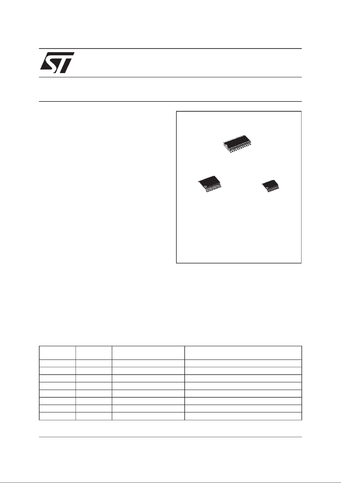
■ PACKAGEDINSO-24,SSO-24AND TSSOP24
PACKAGES
DESCRIPTION
The ST207E is a 5 driver and 3 receiver devices
designedforRS-232 and V.28 communicationsin
harsh enviroments. Each transmitter output and
receiver input is protected against±15KV
electrostaticdischarge (ESD) shocks. The drivers
and receivers of the ST207E meet all
EIA/TIA-232E and CCITT V.28 specifications at
data rates up to 120Kbps, when loaded in
accordancewith the EIA/TIA-232Especification.
The ST207E operateswith four 0.1µF capacitors.
It cames in 24-pinSO and TSSOPpackages.
ST207E
± 15KVESD PROTECTED
5V RS-232 TRANSCEIVER
PRELIMINARY DATA
D
(Micro Package Large)
P
(SSOPPackage)
(TSSOPPackage)
T
ORDERCODES
Type Temperature
Range
ST207ECD 0 to 70
ST207EBD -40 to 85
ST207ECDR 0 to 70
ST207EBDR -40 to 85
ST207ECTR 0 to 70
ST207EBTR -40 to 85
ST207ECPR 0 to 70
ST207EBPR -40 to 85
June 2000
Package Comments
o
C SO-24 (Tube) 33 partsper tube / 25 tube per box
o
C SO-24 (Tube) 33 partsper tube / 25 tube per box
o
C SO-24 (Tape & Reel) 1000 parts per reel
o
C SO-24 (Tape & Reel) 1000 parts per reel
o
C TSSOP24 (Tape & Reel) 2500 parts per reel
o
C TSSOP24 (Tape & Reel) 2500 parts per reel
o
C SSOP24 (Tape & Reel)
o
C SSOP24 (Tape & Reel)
1/9
Page 2

ST207E
PIN CONFIGURATION
PIN DESCRIPTION
PIN No SYM BO L NAM E AND FUNC T I O N
1T3
2T1
3T2
4R1
5R1
6T2
7T1
OUT
OUT
OUT
IN
OUT
IN
IN
8 GND Ground
9V
10 C
CC
+ Terminal For Positive Charge-pump Capacitor
1
11 V+ 2V
12 C
13 C
14 C
- Terminal For Positive Charge-pump Capacitor
1
+ Terminal For Negative Charge-pump Capacitor
2
+ Terminal For Negative Charge-pump Capacitor
2
15 V- -2V
16 R3
17 R3
18 T3
19 T4
20 T5
21 T5
22 R2
23 R2
IN
OUT
IN
IN
OUT
IN
OUT
IN
RS-232 Driver Output
RS-232 Driver Output
RS-232 Driver Output
RS-232 Receiver Input
TTL/CMOS Receiver Outputs. All The Receivers Are Inactive In Sutdown
TTL/CMOS Driver Inputs. Internal Pull-up to V
TTL/CMOS Driver Inputs. Internal Pull-up to V
4.75V to 5.25V Supply Voltage
Generated By The Charge Pump
CC
Generated By The Charge Pump
CC
RS-232 Receiver Input
TTL/CMOS Receiver Outputs. All The Receivers Are Inactive In Sutdown
TTL/CMOS Driver Inputs. Internal Pull-up to V
TTL/CMOS Driver Inputs. Internal Pull-up to V
RS-232 Driver Output
TTL/CMOS Driver Inputs. Internal Pull-up to V
TTL/CMOS Receiver Outputs. All The Receivers Are Inactive In Sutdown
RS-232 Receiver Input
CC
CC
CC
CC
CC
2/9
Page 3
ST207E
ABSOLUTE MAXIMUM RATINGS
(Note 1)
Symb o l Para met er Val u e Uni t
V
V
V
T
R
T
OUT
R
OUT
T
SCTOUT
T
AbsoluteMaximumRatingsarethosevaluesbeyond whichdamagetothedevicemayoccur. Functionaloperationunderthese condition isnotimplied.
Supply Voltage -0.3 to 6 V
CC
Extra Positive Voltage (VCC-0.3) to 14 V
+
Extra Negative Voltage -14 to 0.3 V
-
Transmitter Input Voltage Range -0.3 to (VCC+ 0.3) V
IN
Receiver Input Voltage Range ±30 V
IN
Transmitter Output Voltage Range (V- - 0.3) to (V+ + 0.3) V
Receiver Output Voltage Range -0.3 to (VCC+ 0.3) V
Short Circuit Duration on T
Storage Temperature Range -65 to +150
stg
OUT
Continuous
o
C
ESD PERFORMANCE: TRANSMITTEROUTPUTS, RECEIVER INPUTS
Symbol Parameter Test Conditions Value Unit
Min. Typ. Max.
ESD ESD Protection Voltage Human Body Model ±15 kV
ELECTRICAL CHARACTERISTICS
(C
otherwisespecified. Typical Valus are referredto T
Symbol Parameter Test Conditions Value Unit
I
SUPPLYVCC
Power Supply Current No Load, TA=25oC25mA
= 0.1µF, VCC=5V±5% TA= Min to Max,unless
1-C4
=25oC)
A
Min. Typ. Max.
RECEIVERELECTRICAL CHARACTERISTICS(C1-C4= 0.1µF, VCC=5V±5% TA= Min to Max,
unlessotherwise specified.TypicalValus are referred toT
Symbol Parameter Test Conditions Value Unit
V
V
V
V
R
Receiver Input Voltage
RIN
Operating Range
Input Threshold Low TA=25oC, VCC= 5 V 0.8 1.2 V
RIL
Input Threshold High TA=25oC, VCC= 5 V 1.7 2.4 V
RIH
Input Hysteresis VCC= 5 V, no hysteresis in shutdown 0.2 0.5 1 V
RIHYS
Input Resistance TA=25oC, VCC=5V 357K
RIN
Output Voltage Low 0.4 V
V
OL
Output Voltage High I
V
OH
= -1mA 3.5 VCC-0.4 V
OUT
=25oC)
A
Min. Typ. Max.
-30 30 V
Ω
3/9
Page 4

ST207E
TRANSMITTER ELECTRICAL CHARACTERISTICS
(C
Max, unless otherwise specified. Typical Valus are referred to T
= 0.1µF, VCC=5V±5% TA= Min to
1-C4
=25oC)
A
Symbol Parameter Test Conditions Value Unit
Min. Typ. Max.
V
R
Output Voltage Swing All drivers loaded with 3KΩto GND
TOUT
Transmitter Output Resistance VCC=V+=V-=0V V
OUT
Transmitter Output Short
I
SC
=±2 V 300
OUT
5
±
8.5 V
±
Ω
±18 ±60 mA
Circuit Current
Input Pull-Up Current TIN= 0 V 15 200
I
IL
Input Logic Threshold Low 0.8 V
V
TIL
V
Input Logic Threshold High 2 V
TIH
µ
TIMINGCHARACTERISTICS (C1-C4= 0.1µF, VCC=5V±5% TA= Min to Max, unless otherwise
specified.Typical Valus are referredto T
Symbol Parameter Test Conditions Value Unit
DR Maximum Data Rate R
t
t
t
t
Receiver Propagation Delay All drivers loaded with 3KΩto GND 0.2 10
PLHR
PHLR
Transmitter Propagation Delay RL=3KΩ,CL= 2500pF
PLHT
PHLT
SR Transition-Region Slew Rate T
=25oC)
A
=3KΩto 7 KΩ,
L
C
= 50pF to1000pF
L
one transmitter switching
all transmitters loaded
=25oCVCC=5V
A
=3KΩto 7 KΩ,
R
L
= 50pF to1000pF
C
L
measure from -3V to 3V or 3V to -3V
Min. Typ. Max.
120 kbps
µ
2
µ
3 7 30 V/µs
A
s
s
4/9
Page 5

ST207E
APPLICATION CIRCUITS
(note 1, note2)
Note1:C
Note2:C
capacitorscanevenbe1 µFones.
1-4
canbecommonorbiasedcapacitors.
1-4
CapacitanceValue (µF)
DEVICESC1C2C3C4C5
ST207E 0.1 0.1 0.1 0.1 0.1
5/9
Page 6

ST207E
SO-24 MECHANICALDATA
DIM.
mm inch
MIN. TYP. MAX. MIN. TYP. MAX.
A 2.65 0.104
a1 0.10 0.20 0.004 0.007
a2 2.45 0.096
b 0.35 0.49 0.013 0.019
b1 0.23 0.32 0.009 0.012
C 0.50 0.020
c1 45 (typ.)
D 15.20 15.60 0.598 0.614
E 10.00 10.65 0.393 0.420
e 1.27 0.05
e3 13.97 0.55
F 7.40 7.60 0.291 0.299
L 0.50 1.27 0.19 0.050
S 8 (max.)
L
A
a2
b
e3
D
24 13
112
e
F
s
a1
c1
b1
C
E
P013T
6/9
Page 7

SSOP24 MECHANICAL DATA
ST207E
DIM.
mm inch
MIN. TYP. MAX. MIN. TYP. MAX.
A 2.00 0.079
A1 0.25 0.010
A2 1.51 2.00 0.059 0.079
b 0.25 0.30 0.35 0.010 0.012 0.014
c 0.10 0.35 0.004 0.014
D 8.35 9.35 0.329 0.368
E 7.6 8.7 0.299 0.343
E1 5.02 6.10 6.22 0.198 0.240 0.245
e 0.65 BSC 0.0256BSC
K0
o
10
o
o
0
10
L 0.25 0.50 0.80 0.010 0.020 0.031
o
A2
A
A1
PIN 1 IDENTIFICATION
b
e
K
c
L
E
D
E1
1
7/9
Page 8

ST207E
TSSOP24 MECHANICAL DATA
DIM.
mm inch
MIN. TYP. MAX. MIN. TYP. MAX.
A 1.1 0.433
A1 0.05 0.10 0.15 0.002 0.004 0.006
A2 0.85 0.9 0.95 0.335 0.354 0.374
b 0.19 0.30 0.0075 0.0118
c 0.09 0.2 0.0035 0.0079
D 7.7 7.8 7.9 0.303 0.307 0.311
E 6.25 6.4 6.5 0.246 0.252 0.256
E1 4.3 4.4 4.48 0.169 0.173 0.176
e 0.65 BSC 0.0256BSC
K0
o
o
4
o
8
o
0
o
4
L 0.50 0.60 0.70 0.020 0.024 0.028
o
8
A
PIN 1 IDENTIFICATION
8/9
A2
A1
b
e
K
c
L
E
D
E1
1
Page 9

ST207E
Information furnished isbelieved to be accurate and reliable. However,STMicroelectronics assumes no responsibility for the consequences
of use of such information nor for any infringement of patents or other rights of third parties which may result from its use. No license is
granted by implication or otherwise under any patent or patent rights of STMicroelectronics. Specification mentioned in thispublication are
subject tochange without notice. Thispublication supersedes andreplaces all informationpreviously supplied. STMicroelectronics products
are not authorized for use as critical components in life support devices or systems withoutexpress written approval of STMicroelectronics.
The ST logo isa registered trademark of STMicroelectronics
2000 STMicroelectronics – Printed in Italy– All RightsReserved
STMicroelectronics GROUP OF COMPANIES
Australia - Brazil - China - Finland - France - Germany - Hong Kong - India - Italy - Japan- Malaysia - Malta - Morocco
Singapore - Spain - Sweden - Switzerland - United Kingdom - U.S.A.
http://www.st.com
.
9/9
 Loading...