

Datasheet ST203S10PFJ0L, ST203S10PFJ0, ST203S10MFJ2L, ST203S10MFJ2, ST203S10MFJ1L Datasheet (International Rectifier)
...Page 1

D-470
DISCRETE POWER DIODES and THYRISTORS
DATA BOOK
Page 2
ST203S SERIES
INVERTER GRADE THYRISTORS
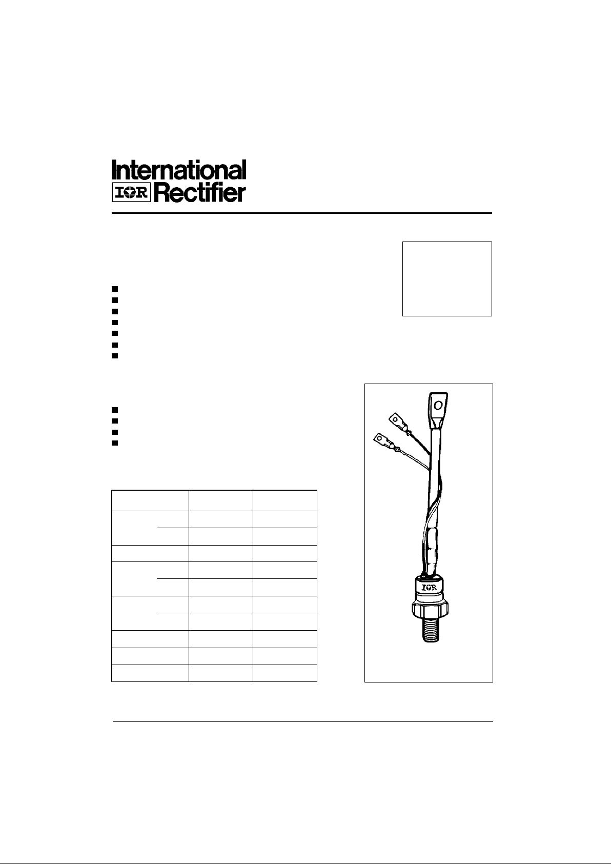
Stud Version
205A
D-471
Bulletin I25177/B
Features
All diffused design
Center amplifying gate
Guaranteed high dv/dt
Guaranteed high di/dt
High surge current capability
Low thermal impedance
High speed performance
Typical Applications
Inverters
Choppers
Induction heating
All types of force-commutated converters
I
T(AV)
205 A
@ T
C
85 °C
I
T(RMS)
320 A
I
TSM
@ 50Hz 5260 A
@ 60Hz 5510 A
I
2
t @ 50Hz 138 KA2s
@ 60Hz 126 KA
2
s
V
DRM/VRRM
1000 to 1200 V
t
q
range 20 to 30 µs
T
J
- 40 to 125 °C
Parameters ST203S Units
Major Ratings and Characteristics
case style
TO-209AB (TO-93)
Page 3
ST203S Series
D-472
Voltage V
DRM/VRRM
, maximum V
RSM
, maximum I
DRM/IRRM
max.
Type number Code repetitive peak voltage non-repetitive peak voltage
@ TJ = TJ max.
V V mA
10 1000 1100
12 1200 1300
ELECTRICAL SPECIFICATIONS
Voltage Ratings
ST203S 40
Frequency Units
50Hz 580 400 900 640 6180 4680
400Hz 570 380 940 650 2980 2150
1000Hz 520 320 930 630 1730 1200 A
2500Hz 370 210 780 510 890 580
Recovery voltage Vr 50 50 50 50 50 50
Voltage before turn-on Vd V
DRM
V
DRM
V
DRM
Rise of on-state current di/dt 50 50 - - - - A/µs
Case temperature 60 85 60 85 60 85 °C
Equivalent values for RC circuit 47Ω / 0.22µF 47Ω / 0.22µF 47Ω / 0.22µF
I
TM
180oel
180
o
el
100µs
I
TM
I
TM
Current Carrying Capability
V
I
T(AV)
Max. average on-state current 205 A 180° conduction, half sine wave
@ Case temperature 85 °C
I
T(RMS)
Max. RMS on-state current 320 DC @ 76°C case temperature
I
TSM
Max. peak, one half cycle, 5260 t = 10ms No voltage
non-repetitive surge current 5510 A t = 8.3ms reapplied
4420 t = 10ms 100% V
RRM
4630 t = 8.3ms reapplied Sinusoidal half wave,
I
2
t Maximum I2t for fusing 138 t = 10ms No voltage Initial TJ = TJ max
126 t = 8.3ms reapplied
98 t = 10ms 100% V
RRM
89 t = 8.3ms reapplied
I
2
√t Maximum I2√t for fusing 1380 KA2√s t = 0.1 to 10ms, no voltage reapplied
Parameter ST203S Units Conditions
On-state Conduction
KA2s
Page 4

ST203S Series
D-476
Fig. 3 - On-state Power Loss Characteristics
Fig. 1 - Current Ratings Characteristics Fig. 2 - Current Ratings Characteristics
Fig. 4 - On-state Power Loss Characteristics
Page 5

ST203S Series
D-477
Fig. 7 - On-state Voltage Drop Characteristics
Fig. 8 - Thermal Impedance Z
thJC
Characteristic
Fig. 10 - Reverse Recovery Current Characteristics
Fig. 9 - Reverse Recovered Charge Characteristics
Fig. 5 - Maximum Non-repetitive Surge Current
Fig. 6 - Maximum Non-repetitive Surge Current
Page 6

ST203S Series
D-478
Fig. 13 - Frequency Characteristics
Fig. 11 - Frequency Characteristics
Fig. 12 - Frequency Characteristics
Page 7

ST203S Series
D-479
Fig. 14 - Maximum On-state Energy Power Loss Characteristics
Fig. 15 - Gate Characteristics
Page 8

ST203S Series
D-473
VTMMax. peak on-state voltage 1.72 ITM= 600A, TJ = TJ max, tp = 10ms sine wave pulse
V
T(TO)1
Low level value of threshold
voltage
V
T(TO)2
High level value of threshold
voltage
r
t
1
Low level value of forward
slope resistance
r
t
2
High level value of forward
slope resistance
I
H
Maximum holding current 600 TJ = 25°C, IT > 30A
I
L
Typical latching current 1000 TJ = 25°C, VA= 12V, Ra = 6Ω, IG= 1A
Parameter ST203S Units Conditions
On-state Conduction
1.17 (16.7% x π x I
T(AV)
< I < π x I
T(AV)
), TJ = TJ max.
1.20 (I > π x I
T(AV)
), TJ = TJ max.
V
0.92 (16.7% x π x I
T(AV)
< I < π x I
T(AV)
), TJ = TJ max.
0.87 (I > π x I
T(AV)
), TJ = TJ max.
mΩ
mA
di/dt Max. non-repetitive rate of rise T
J
= TJ max, V
DRM
= rated V
DRM
of turned-on current I
TM
= 2 x di/dt
T
J
= 25°C, V
DM
= rated V
DRM, ITM
= 50A DC, tp= 1µs
Resistive load, Gate pulse: 10V, 5Ω source
T
J
= TJ max, I
TM
= 300A, commutating di/dt = 20A/µs
V
R
= 50V, tp = 500µs, dv/dt: see table in device code
Switching
Parameter ST203S Units Conditions
1000 A/µs
t
d
Typical delay time 0.79
Min Max
dv/dt Maximum critical rate of rise of T
J
= TJ max., linear to 80% V
DRM
, higher value
off-state voltage available on request
I
RRM
Max. peak reverse and off-state
I
DRM
leakage current
Parameter ST203S Units Conditions
Blocking
500 V/µs
40 mA T
J
= TJ max, rated V
DRM/VRRM
applied
PGMMaximum peak gate power 60
P
G(AV)
Maximum average gate power 10
I
GM
Max. peak positive gate current 10 A TJ = TJ max, tp ≤ 5ms
+V
GM
Maximum peak positive
gate voltage
-V
GM
Maximum peak negative
gate voltage
I
GT
Max. DC gate current required
to trigger
V
GT
Max. DC gate voltage required
to trigger
I
GD
Max. DC gate current not to trigger 20 mA
V
GD
Max. DC gate voltage not to trigger 0.25 V
Triggering
Parameter ST203S Units Conditions
20
5
V TJ = TJ max, tp ≤ 5ms
200 mA
3 V
T
J
= 25°C, VA = 12V, Ra = 6Ω
TJ = TJ max, rated V
DRM
applied
µs
W TJ = TJ max, f = 50Hz, d% = 50
t
q
Max. turn-off time 20 30
Page 9

ST203S Series
D-474
Ordering Information Table
TJMax. junction operating temperature range -40 to 125
T
stg
Max. storage temperature range -40 to 150
R
thJC
Max. thermal resistance, junction to case 0.105 DC operation
R
thCS
Max. thermal resistance, case to heatsink 0.04 Mounting surface, smooth, flat and greased
T Mounting torque, ± 10% 31 Nm
(275) (Ibf-in)
24.5 Nm
(210) (Ibf-in)
wt Approximate weight 280 g
Case style TO-209AB (TO-93) See Outline Table
Parameter ST203S Units Conditions
Thermal and Mechanical Specifications
°C
K/W
Non lubricated threads
180° 0.016 0.012
120° 0.019 0.020
90° 0.025 0.027 K/W T
J
= TJ max.
60° 0.036 0.037
30° 0.060 0.060
Conduction angle Sinusoidal conduction Rectangular conduction Units Conditions
5
6
8
9
ST 20 3 S 12 P F J 0
3
4
10
7
Device Code
1
2
Lubricated threads
1 - Thyristor
2 - Essential part number
3 - 3 = Fast turn off
4 - S = Compression bonding Stud
5 - Voltage code: Code x 100 = V
RRM
(See Voltage Ratings table)
6 - P = Stud base 3/4" 16UNF-2A
M = Stud base metric threads M16/ x 1.5
7 - Reapplied dv/dt code (for t
q
test condition)
8 - t
q
code
9 - 0 = Eyelet terminals (Gate and Aux. Cathode Leads)
1 = Fast-on terminals (Gate and Aux. Cathode Leads)
2 = Flag terminals (For Cathode and Gate Terminals)
- Critical dv/dt:
None = 500V/µsec (Standard value)
L = 1000V/µsec (Special selection)
dv/dt - t
q
combinations available
dv/dt (V/µs) 20 50 100 200 400
20 CK DK EK -- -25 CJ DJ EJ FJ * -30 CH DH EH FH HH
tq(µs)
∆R
thJC
Conduction
(The following table shows the increment of thermal resistence R
thJC
when devices operate at different conduction angles than DC)
*Standard part number.
All other types available only on request.
10
Page 10

ST203S Series
D-475
Case Style TO-209AB (TO-93)
All dimensions in millimeters (inches)
Fast-on Terminals
Outline Table
C.S. 0.4 mm
2
10 (0.39)
RED SHRINK
RED CATHODE
RED SILICON RUBBER
4.3 (0.17) DIA
21 (0 .8 3)
12.5 (0.49) MA X .
15 7 (6.18)
170 (6.69 )
(.0006 s.i.)
8.5 (0.33) DIA.
16.5 (0.65) MAX.
MAX.
70 (2.75) M IN .
CERAMIC HOUSING
22.5 (0.88) MAX. DIA.
29 (1 .14) MAX.
SW 27
C.S. 16mm
2
FLEXIBLE LEAD
(.025 s.i.)
2.6 (0.10) MAX.
WHITE SHRINK
2
0
(
0
.
7
9
)
M
I
N
.
29.5 (1.16)
MAX.
1/2"-20UNF-2A
9
.
5
(
0
.
3
7
)
M
I
N
.
WHITE GATE
215 (8.46)
Case Style TO-209AB (TO-93) Flag
All dimensions in millimeters (inches)
CERAMIC HOUSING
27 .5 (1 .08 ) M A X .
38 .5 (1 . 5 2 ) M A X .
3 (0.12)
8 0 ( 3 .15 ) M A X .
DIA. 27.5 (1.08) MAX.
1 6 (0 .63 ) M A X .
FLAG TERMINALS
1.5 (0.06) DIA.
SW 32
22 (0.89)
DIA. 6.5 (0.25)
13 (0. 5 1)
14 (0.55)
*FOR METRIC DEVICE. M16 X 1.5 - LENGHT 21 (0.83) MAX.
3/4"-16UNF-2A*
AMP. 280000-1
REF-250
 Loading...