

Page 1

12 January 98 42 1714 01
The information in this datasheet is subject to change 1/66
ST18952
DIGITAL SIGNAL PROCESSOR (DSP) CHIP
PRELIMINARY DATA
■ Programmable D950 Core
■ Data calculation unit
■ Address calculationunit
■ Program control unit
■ Fast and flexible buses
■ 66MIPS - 15 ns instruction cycle time
■ 16.5 Kwords data memory (RAM)
■ 32 Kwords program memory (RA42 1714 01)
■ Interrupt controller
■ DMA controller
■ Serial input/output
■ Timer
■ Bus switch unit
■ Emulation unit
■ JTAG IEEE 1149.1 test access port
TAP
Emulation
unit
2
Timers
2
Serial I/O
Interrupt
controller
16.5 Kwords
data memory
Bus switch
unit
DMA
controller
D950
core
32 Kwords
program
memory
Page 2

2/66
Table of Contents
3
1 Introduction . . . . . . . . .................................................. 4
2 Pin Description . . . . . ..................................................5
3 Functional Overview . . . . . . . . . . . . . . . . . . .................................9
4 D950Core ..........................................................12
4.1 D950Core registers . . . . . . . . ....................................... 14
5 Memory ............................................................ 15
5.1 Internal memory resource . . . ....................................... 15
5.2 Direct bus extension . . . . . . . . . . . . . . . . . . . . . . . . . .....................16
6 Bus Switch Unit . . . . . . . . . . . . . . . . . . . . . . . . . ............................. 18
6.1 BSUoperation ................................................... 18
6.2 BSU control registers . . . . . . . ....................................... 19
7 DMA Controller . . . . . ................................................. 21
7.1 DMA operation . . . . ...............................................22
7.2 DMA registers . . . . . . . ............................................23
8 Interrupt Controller . . . . . ............................................... 26
8.1 Interrupt controller registers . . . . . . . . .................................27
9 Timers ............................................................. 31
9.1 Timerregisters................................................... 31
10 SIO ...............................................................35
10.1 SIO registers . . . . . . . . . . . . . . . . . ...................................35
11 External Coprocessor . . . . . ............................................41
12 SystemControl ......................................................41
12.1 System registers .................................................42
12.2 Clocks . . . . . . . . . . . . . . . . . . . . . . . . . . . . . . . ..........................44
13 JTAG IEEE 1149.1 test access port ...................................... 45
14 Emulation Unit . . . . . . .................................................45
15 Electrical Specifications ................................................47
15.1 DC Absolute maximum ratings ...................................... 47
15.2 DC Electrical characteristics . . . . . . . . . . . . . . . . ........................47
15.3 AC Characteristics . . . .............................................48
16 Y SPACE Memory Mapping . . . . . ....................................... 56
16.1 Memorymap ....................................................56
16.2 Serial input/output registers . . . . . . . . . . . . . . . . . ........................56
16.3 Timerregisters...................................................58
16.4 Bus switch unit registers . . . . . . . . . . .................................58
1
Page 3

3/66
Table of Contents
16.5 System control registers . . . . . . . . . . ................................. 58
16.6 DMA controller registers . . . . . . . . . . . . . ..............................59
16.7 Interrupt controller registers . . . . . . . . . . . . . . . . . . . . . . . . . . . . .............59
16.8 Emulation unit registers . . . . . . . . . . . . . . .............................. 60
16.9 D950Core control registers . . . . . . . . . . . . . . . . . . . . . . . .................. 60
17 ST18952 Package Specifications . .......................................61
17.1 208 pin PQFP pinout . . . . . . . . . . ....................................61
17.2 208 pin PQFP package dimensions . . . . . .............................62
18 DeviceID...........................................................64
19 Ordering Information . . . . . . . . . . . . ......................................64
20 Revision History . . . . . . . ............................................... 64
Page 4

4/66
ST18952
1 Introduction
The ST18952 chip includes the SGS-Thomson D950 16-bit fixed point digital signal processor
core, 16.5 Kwords of data memory, 32 Kwords of program memory, and the following on-chip
peripherals:
• Interrupt controller (ITC)
• DMA controller (DMA)
• Bus switch unit (BSU)
• Synchronous input/output (SIO)
• Timer (TIM)
• Emulation unit (EMU)
• Tap controller (TAP)
It also includes an oscillator and a PLL for generation of the D950Core clock.
The ST18952 is used on the D950 Emulation Card (called the D952 module) developed by
SGS-Thomson.
It can also be used for application development by customers.
Custom development is eased by providing direct access to the D950 instruction and data
buses to allow simultaneous access to external memories or peripherals (with wait-states).
For full details of the D950Core refer tothe D950Core datasheet (
document number 42-1709
).
2
Page 5

5/66
ST18952
2 Pin Description
The following tables detail the ST18952 pin set. There is one table for each group of pins. The
tables detail the pin name, type and a short description of the pin function.
Signal names have an overbar if they are active low, otherwise they are active high.
Table 2.1 Direct I bus extension (35 pins)
Table 2.2 Direct Y bus extension (35 pins)
Table 2.3 Direct X bus extension / bus extension through bus switch unit (39 pins)
Pin name Type Description
IDE0-15 I/O Instruction data extension bus.
IAE0-15 O Instruction address extension bus.
IRDE O I-extension bus read strobe. Active low.
IWRE O I-extension bus write strobe. Active low.
IBSE O I-extension bus strobe. Active low.
Pin name Type Description
YDE0-15 I/O Y data extension bus.
YAE0-15 O Y address extension bus.
YRDE O Y-extension bus read strobe. Active low.
YWRE O Y-extension bus write strobe. Active low.
YBSE O Y-extensionbus strobe. Active low.
Pin name Type Description
ED_XDE0-15 I/O Multiplexed input/output. Bus switchunit extension data bus or X data exten-
sion bus.
EA_XAE0-15 O Multiplexed output. Bus switch unit extension address bus or X address ex-
tension bus.
EIRD O BSU EIRD output
EIWR O BSU EIWR output
XBSE O X extension bus data strobe
EYRD O BSU EYRD output
EYWR O BSU EYWR output
XRDE_EXRD O Multiplexed output.
X-extension bus read strobe (XRDE) or BSU EXRD output.
XWRE_EXWR O Multiplexed output.
X-extension bus write strobe (XWRE) or BSUEXWR output.
Page 6

6/66
ST18952
Table 2.4 General purpose parallel port / Interrupt requests (8 pins)
Table 2.5 Clocks (6 pins)
Table 2.6 Bus control (3 pins)
Pin name Type Description
P_ITRQ0-7 I/O Multiplexed input/output. Parallel port I/O or external interrupt request (ITRQ).
Pin name Type Description
EXTAL I Oscillator input.
XTAL O Oscillator output. Nominal oscillator frequency is 27 MHz.
MCLK I Master clock input (use of external clock generator).
CLK_MODE I Clock mode select input.
When low the oscillator and internal PLL are enabled. The 950 receives its
Master clock from the PLL at 5 times the oscillator frequency.
When high the PLL is disabled. The D950 receives its master clock from
MCLK.
INCYCLE O Instruction cycle.
Asserted high for 1 CLKOUT cycle at the beginning of instruction cycle.
CLKOUT O Output clock (at input clock/2 frequency).
Pin name Type Description
DTACK I Data transfer acknowledge input. Active low.
It is combined in a ORgate with BSU DTACK output in order to generate the
DTACK signal for the D950Core. It controls extension of bus cycles by inser-
tion of wait-states whenusing external memory either through Bus-switch or
direct extension.
HOLD I External Bus Hold request input. Active low.
HOLDACK O Hold acknowledge output. Active low.
Page 7

7/66
ST18952
Table 2.7 D950Core control (10 pins)
Table 2.8 Emulation unit (7 pins)
Pin name Type Description
RESET I Reset input. Active low.
Initializes the 950-Core to the RESET state.
RESET_OUT O Reset output (system reset). Active low.
LP I Low power input. Active low.
LPACK O Low power acknowledge. Active low.
MODE I Mode selection for Reset.
0: forces reset address to 0x0000
1: forces reset address to 0xFC00
IRD_WR O Program memory read/write indicator.
VCI O Valid coprocessor instruction output.
Asserted low during the instruction cycle preceding a coprocessor instruc-
tion to enable operation of an external coprocessor.
STACKX O X stack read/write instruction flag.
STACKY O Y stack read/write instruction flag.
IDT_EN I I-bus direct transfer enable (to BSU peripheral). Active low.
Pin name Type Description
ERQ I Emulator Halt Request. Active low.
Halts program execution and enters emulation mode.
IDLE O Output flag assertedhigh when the processoris halted dueto an emulation
halt request or a valid breakpoint condition.Asserted low when the processor is not Halted or during execution ofan instruction under control of the
emulator.
HALTACK O Halt acknowledge. Active high.
Asserted highwhen the processor is halted from anEmulator Halt request
or when a valid Breakpoint condition is met.
SNAP O Snapshot. Active high.
Asserted highwhen executing an instructionif Snapshot modeis enabled.
AXEBP I Enable breakpoint on X address buswhen high.
AYEBP I Enable breakpoint on Y address buswhen high.
AIEBP_SCAN_EN I Enable breakpoint on I address bus when high.
Page 8

8/66
ST18952
Table 2.9 JTAG IEEE 1149.1 test access port (5 pins)
Table 2.10 DMA controller / Serial input/output (8 pins)
Pin name Type Description
TDI I Test data input.
TCK I Test clock.
TMS I Test mode select.
TDO O Test data output.
TRST I Test logic reset (also used for Emulator module). Active low.
Pin name Type Description
DMARQ0/SRD0 I DMA request 0or SIO0 Receive data
DMARQ1/SCK0 I/O DMA request 1 or SIO0 Data clock
DMARQ2/SRD1 I DMA request 2or SIO1 Receive data
DMARQ3/SCK1 I/O DMA request 3 or SIO1 Data clock
DMACK0/STD0 O DMA acknowledge 0 or SIO0 Transmit data
DMACK1/SFS0 I/O DMA acknowledge 1 or SIO0 Frame synchronizer
DMACK2/STD1 O DMA acknowledge 2 or SIO1 Transmit data
DMACK3/SFS1 I/O DMA acknowledge 3 or SIO1 Frame synchronizer
Page 9
9/66
ST18952
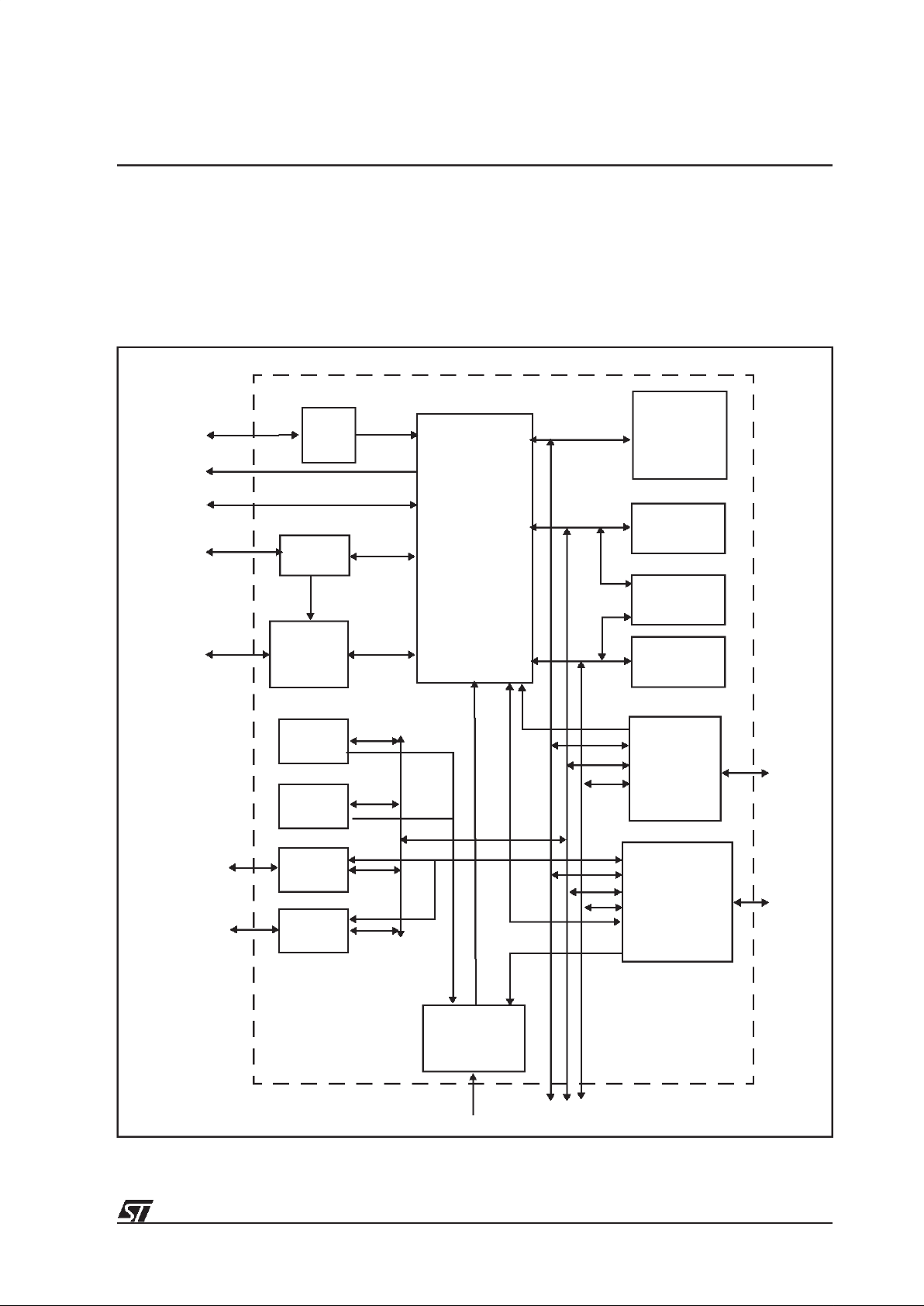
3 Functional Overview
A block diagram of the ST18952 isshown below. The modules that comprise the ST18952 are
outlined in this section and described in detail in the following sections.
Figure 3.1 ST18952 block diagram
Y
X
D950Core
DMA
TAP
Interrupt
8k x 16
Bus
8k x 16
8k x 16
I
OSC
+
PLL
X/Y
0.5k x 16
Emulation
Control I/Os/ Port
JTAGPort
(x 4)
Output clocks
Input clock + control
Timer 0
SIO 1
Timer 1
SIO 0
controller
switch
unit
unit
controller
Direct extension buses
Ext. bus
Page 10

10/66
ST18952
D950Core
The D950Core is a general purpose programmable 16-bit fixed point Digital Signal Processor
Core. The main blocks of the D950Core include an arithmetic data calculation unit, a program
control unit and an address calculation unit, able to manage up to 64k (program) and 128k
(data) x 16-bit memory spaces.
Memory
One 32 Kword and two 8 Kword single port memories are included on-chip:
• 32 Kword instruction memory on I space
• 8 Kword X-Data memory on X space
• 8 Kword Y-Data memory on Y space
One 512 word dual port memory is shared on X and Y spaces.
Memory can be extended off-chip for all three spaces in two ways:
1: Directly - Accesses to program and data memories can be performed simulta-
neously. Insertion of wait-states is necessary in case of nominal frequency
work.
2: Through the bus switch unit - Accesses to the different external spaces are mul-
tiplexed and wait-states are added.
Bus switch unit
The bus switch unit (BSU) is a bi-directional switcher which switches the 3 internal buses (I, X
and Y) to the external (E) bus.
DMA controller
The DMA controller manages data transfer between memories and external peripherals.
There are four independent DMA channels. Transfers can occur on X/Y/I spaces
(simultaneous transfers on X and Y spaces).
Interrupt controller
The interrupt controller (ITC) can manage up to eight external interrupts. Each source can be
individually activated and programmed as edge or level triggered. A ‘pending interrupt’ flag
displays the source waiting for service (this flag is writable to allow a software interrupt
capability). The priority of interrupts is programmable.
Timers
There are two timer (TIM) units on the ST18952. The timers enable interrupts to be generated
after predefined periods of time.
Page 11

11/66
ST18952
SIO
There are two synchronous serial input/output (SIO) ports enable a link to serial devices such
as codecs and to other processors.
Oscillator and PLL
A 27 MHz crystal can be used with the on-chip oscillator and PLL to provide the D950Core
clock input. The PLL module multiplies the oscillator frequency by a factor of 10 and generates
a 270 MHz signal. A programmable divider is connected to the PLL output to generate the
D950 clock input. The division range is 2 to 256.
Emulation unit and JTAG IEEE 1149.1 test access port
The emulation unit (EMU) performs functions dedicated to emulation and test through the
external IEEE 1149.1 JTAG interface.
Page 12

12/66
ST18952
4 D950Core
The D950Core is composed of three main units.
• Data Calculation Unit (DCU)
• Address Calculation Unit (ACU)
• Program Control Unit (PCU)
For full details of the D950 DSP core refer to the D950Core datasheet (
document number 42-
1709
).
These units are organized in an HARVARD architecture around three bidirectional 16-bit
buses, two for data and one for instruction. Each of these buses is dedicated to an unidirectional 16-bit address bus (XA/YA/IA).
An 8-bit general purpose parallel port (P0-P7) can be configured (input or output). A test
condition is attached to each bit to test external events.
The D950Core is controlled through interface pins related to interrupt, low-power mode, reset
and miscellaneous functions.
Figure 4.1 D950Core block diagram
DATA
CALCULATION
UNIT
ADDRESS
CALCULATION
UNIT
PROGRAM
CONTROL
UNIT
CLKIN
DATA MEMORY
PROGRAM MEMORYVDD
VSS
TEST & EMULATIONPO/P7
CONTROL
11
8
14
XD-bus
YD-bus
6
16
16
16
16
3
16
16
OUTPUT
CLOCKS
XA-bus
YA-bus
ID-bus
IA-bus
Control
Page 13
13/66
ST18952
Data buses (XD/YD and XA/YA) are provided externally. Data memories (RAM, ROM) and
peripherals registers are mapped in these address spaces.
Instruction bus (ID/IA) gives access to program memory (RAM, ROM). Each bus has its own
control interface.
Table 4.1 Data/instruction bus and corresponding address bus.
Depending on the calculation mode, the D950Core DCU computes operands which can be
considered as 16 or 32-bit, signed or unsigned. It includes a 16 x 16-bit parallel multiplier able
to implement MAC-based functions in one cycle per MAC. A 40-bit arithmetic and logic unit,
including an 8-bit extension for arithmetic operations, implements a wide range of arithmetic
and logic functions. A 40-bit barrel shifter unit and a bit manipulation unit are included.
The tables below illustrate the different types of word length and word format available for
manipulation.
Table 4.2 Summary of possible word lengths and formats
Data/instruction bus Corresponding address bus
XD Bidirectional 16-bit XA Unidirectional 16-bit
YD Bidirectional 16-bit YA Unidirectional 16-bit
ID Bidirectional 16-bit IA Unidirectional 16-bit
0 1-bit word
7 0 8-bit word
15 0 16-bit word signed / unsigned
31 16 15 0 32-bit word signed / unsigned
39 32 31 16 15 0 40-bit word signed / unsigned
Format Minimum Maximum
fractional signed - 1 + 0.999969481
unsigned 0 + 0.99996948
integer signed - 32768 + 32767
unsigned 0 + 65535
Page 14

14/66
ST18952
4.1 D950Core registers
PCDR
The Port Control Direction register defines the data direction of each port pin. After reset,
PCDR default value is 0 (Port pins are configured as inputs)
PCSR
The Port Control Sensitivity register defines sensitivity of each port pin. After reset, PCSR
default value is 0 (Port pins are configured as level-sensitive).
Register Function
BX Modulo base address for X-memory space
MX Modulo maximum address for X-memory space
BY Modulo base address for Y-memory space
MY Modulo maximum address for Y-memory space
POR Port Output Register - 8LSB are significant, 8MSB are undefined when reading
PIR Port Input Register
PCDR Port Control Direction Register
PCSR Port Control Sensitivity Register
1514131211109876543210
--------P7DP6DP5DP4DP3DP2DP1DP0D
Bit Function
PiD Port pin direction
0: Input port pin (def.)
1: Output port pin
Bits 8 - 15 RESERVED (read: undefined, write: don’t care)
1514131211109876543210
--------P7SP6SP5SP4SP3SP2SP1SP0S
Bit Function
PiS Port pin sensitivity
0: Level sensitive (def.)
1: Edge sensitive
Bits 8 - 15 RESERVED (read: undefined, write: don’t care)
Page 15
15/66
ST18952
5 Memory
5.1 Internal memory resource
One 32 Kword and two 8 Kword single port memories are included on-chip:
• Instruction memory on I space from address 0 to 32767 (32 K)
• X-Data memory on X space from address 0 to 8191 (8 K)
• Y-Data memory on Y space from address 0 to 8191 (8 K)
One 512 word dual port memory is shared on X and Y spaces, from addresses 8192 (8 K) to
8703 (8.5K). This is represented graphically below.
Note: the first 256 addresses of the Y space are reserved for the D950 memory-mapped
registers and for on-chip memory mapped peripherals.
Memory can be extended off-chip for all three spaces in two ways:
1: Directly - Accesses to program and data memories can be performed simulta-
neously. Insertion of wait-states is necessary in case of nominal frequency
work.
2: Through the bus switch unit - Accesses to the different external spaces are mul-
tiplexed and wait-states are added.
The specific details on the operation of the BSU are described separately in ”Bus Switch Unit”
on page 18.
Figure 5.1 Memory mapping
0000
1FFF 8k
32k
FFFF
64k
64k
Internal SPRAM
Internal SPRAM
Registers
External
Internal SPRAM
ExternalExternal
All addresses are hexadecimal
Internal DPRAM
Internal DPRAM
21FF
8.5k
0100
64k
8k
8.5k
FFFF
8000
1FFF
FFFF
21FF
External memory is accessed directly or through the bus switch
X-memory I-memoryY-memory
Page 16

16/66
ST18952
5.2 Direct bus extension
Direct extension for I-memory
The internal program memory is used from address 0 to 32767 (32 K). Note, no detection is
provided when an internal space is declared as an external one for the BSU.
The I-bus direct transfer enable signal (IDT_EN) determines whether an access is made
directly to external memory or via the BSU. If reset occurs with the MODE signal set to ‘1’
(select reset address to xFC00), then
• if IDT_EN input = 0: access to external memory is through the BSU
• if IDT_EN input = 1: access to direct external memory space
IAE/IBSE/IRDE/IWRE are always driven except in the case of an external HOLD request.
Note: an external coprocessor will work only when executing program in the external space.
IDE bus is an output only when a direct external write is detected. IDE bus is an input in the
case of:
• an external memory read
• DMA (write) transfers between an external peripheral and internal memory
Direct extension for X-memory
The internal X memory is used from address 0 to 8703 (8.5 K). It is extended with external
memory from address 8704 (8.5K) to 65535 (64K) with the XE bus extension.
The direct extension is managed by the bus switch unit. When the EN_X bit of the BSU XER
register (see ”XER0/1: X-memory space control registers” on page 20) isset to ‘0’, it generates
only software wait-states and access is direct. If the EN_X bit is set to ‘1’, data goes via the
BSU.
X extension and bus switch share the same I/O’s.
Direct extension for Y-memory
The internal Y memory is used from address 0 to 8703 (8.5 K). It is extended with external
memory from address 8704 (8.5 K) to 65535 (64 K) with the YE bus extension.
Address 0 to 256 of the Y space are reserved for memory mapped registers.
Note: The BSU and X direct extension share the same I/O, therefore extension of IE through
the BSU is not possible when direct extension is selected for X/Y. Some combinations of the
EN_I, EN_X and EN_Y bits of the BSU control registers IER/XER/YER are not allowed, as
shown in Table 5.1 below.
Page 17

17/66
ST18952
Table 5.1 Possible BSU register settings
EN_I EN_X EN_Y Operation Allowed or forbidden
1 1 1 Exchanges enabled on I/X/Y spaces Allowed
1 1 0 Exchanges enabled on I and X spaces
Only DTACK generation on Y space
Allowed
1 0 1 Exchanges enabled on I and Y spaces
Only DTACK generation on X space
Forbidden
(X direct & I/Y through BSU)
1 0 0 Exchanges enabled on I space
Only DTACK generation on X and Y spaces
Forbidden
(X direct & I through BSU)
0 1 1 Exchanges enabled on X and Y spaces
Only DTACK generation on I space
Allowed
0 1 0 Exchanges enabled on X space
Only DTACK generation on I and Y spaces
Allowed
0 0 1 Exchanges enabled on Y space
Only DTACK generation on I and X spaces
Forbidden
(X direct & Y through BSU)
0 0 0 No exchange
Only DTACK generation on I, X and Y spaces
Allowed
Page 18

18/66
ST18952
6 Bus Switch Unit
The three memory spaces can be extended off-chip through the bus switch unit (BSU)
peripheral. The figure below shows the layout of the D950Core BSU.
Figure 6.1 D950Core Bus Switch Unit
6.1 BSU operation
The BSU recognizes a bus cycle when a bus extension strobe (IBSE, XBSE or YBSE) goes
active. The BSU decodes the address value to determine if an external memory access is
requested on the I, X or Y-bus and generates the appropriate signals on the external bus side.
The BSU generates software wait-states, depending on the setting of the control register.
If more than one external memory access is attempted at one instruction cycle, they are
serviced sequentially in the following order: I-bus, X-bus, Y-bus.
Each external access requires one basic instruction clock cycle (2 CLKIN cycles), extended
by, at least, one wait-state (2 CLKIN cycles). The number of wait-states can be extended,
either by software with the BSU control registers (see Section 6.2), or by hardware with the
DTACK input signal.
EA
ED
ID
IA
YD
YA
XA
XD
D950Core
BUS
SWITCH
UNIT
DTACK
AS-DSP
BSU_CLK RESET
IRD/XRD/YRD
IWR/XWR/YWR
IBS/XBS/YBS
16
16
16
16
INTERNAL MEMORIES
& PERIPHERALS
16
16
16
16
P
MEM.
X
MEM.YMEM.
222
DTACKin
EYRD/DS
EYWR/RD
EIRD/DS
EIWR/RD
EXRD/DS
EXWR/RD
VR02020A
INTERNAL MEMORIES
& PERIPHERALS
INTERNAL MEMORIES
&PERIPHERALS
DEID/DEXD/DEYD
IID/IXD/IYD
IDT_EN
Page 19

19/66
ST18952
6.2 BSU control registers
The BSU is programmed by six control registers mapped in the Y-memory space. These
define the type of memory used, internal to external boundary address crossing, exchange
type (external direct or through the BSU) and software wait-states count.
There are 2 registers per memory space, making itpossible to define 2 sets of boundaries and
wait state numbers.
Figure 6.2 Default and user mapping examples
The BSU control registers include a reference address on bits 4 to 9, where the internal/
external memory boundary value is stored (see Figure 6.2), and software wait-states count on
bits 0 to 3, allowing up to 16 wait-states.
External addressing is recognized by comparing these address bits for each valid address
from IA, XA and YA, to the reference address contained into the corresponding control
register.
If the address is greater or equal to the reference value, an external access proceeds.
In the following register descriptions, ‘-’ means RESERVED (read: 0, write: don’t care).
EXTERNAL
INTERNAL1
64K
63K
62K
INTERNAL0
DEFAULT MAPPING (RESET)
USER MAPPING
(CAN CHANGE BY 1K STEP)
VALUE 1
VALUE 0
VALUE 1
VALUE 0
EXTERNAL
INTERNAL1
INTERNAL0
64K
0
0
Page 20

20/66
ST18952
XER0/1: X-memory space control registers
After reset, XER0/1 default values are 0x83EF/0x83FF
YER0/1: Y-memory space control registers
After reset, YER0/1 default values are 0x83EF/0x83FFI
IER0/1: Instruction memory control registers
After reset, IER0/1 default values are 0x83EF/0x83FF or 0xC3EF/0xC3FF
(the EN_I value depends on the IDT_EN input value
1514131211109876543210
IM EN_X - - - - XA15 XA14 XA13 XA12 XA11 XA10 W3 W2 W1 W0
Bit Function
W3:0 Wait state count (1 to 16) for off-chip access (X-memory space)
XA15:10 X-memory space map for boundary on-chip or off-chip
EN_X Enable for X-space data exchanges
IM Intel/Motorola
0: Motorola type for memories
1: Intel type for memories (default)
15 14 13 12 11 10 9 8 7 6 5 4 3 2 1 0
IM EN_Y - - - - YA15 YA14 YA13 YA12 YA11 YA10 W3 W2 W1 W0
Bit Function
W3:0 Wait state count (1 to 16) for off-chip access (Y-memory space)
YA15:10 Y-memory space map for boundary on-chip or off-chip
EN_Y Enable for Y-space data exchanges
IM Intel/Motorola
0: Motorola type for memories
1: Intel type for memories (default)
1514131211109876543210
IM EN_I ----IA15 IA14 IA13 IA12 IA11 IA10 W3 W2 W1 W0
Bit Function
W3:0 Wait state count (1 to 16) for off-chip access (I-memory space)
IA15:10 I-memory space map for boundary on-chip or off-chip
EN_I Enable for I-space data exchanges
IM Intel/Motorola
0: Motorola type for memories
1: Intel type for memories (default)
Page 21

21/66
ST18952
7 DMA Controller
The DMA controller manages data transfer between memories and external peripherals and
has the following features:
• four independent DMA channels
• transfers on X / Y / I spaces (simultaneous transfers on X and Y spaces)
• cycle stealing operation:
• 3cycles for a single data transfer (+1cycle for transfers on I space)
• (n+2) cycles for an n-data block transfer (+1cycle for transfers on I space)
• each channel has:
• 3 signals: request (DMARQ), acknowledge (DMACK), interrupt request (DIT)
• 4x16 bit registers for block transfer facilities
• fixed priority between the four channels (highest channel 0, lowest channel 3)
The DMA controller DMARQ0-3 inputs and DMACK0-3 outputs are available as primary
inputs, in the case of SIO inhibition. This is set by the DMAR register (see ”DMAR: DMA
management register” on page 44).
Figure 7.1 DMA controller
YD
YA
16
16
D950Core
INTERRUPT
CONTROLLER
PERIPHERAL
RESET
AS-DSP
HOLD
HOLDACK
INCYCLE
DMA CONTROLLER PERIPHERAL
DMARQ0
DMARQ1
DMARQ2
DMARQ3
DMACK0
DMACK1
DMACK2
DMACK3
DTACK
DIP_ENA
16 16 16 16
IA ID XA XD
IRD
IWR
IBS
XRD
XWR
XBS
YRD
YWR
YBS
DIT0 DIT1 DIT2 DIT3 DIT_AND
3
3
3
CLK
DMA_CLK
Page 22

22/66
ST18952
7.1 DMA operation
The DMA controller interface contains four independent channels allowing data transfer on Imemory space and simultaneous data transfer on X and Y-memory spaces. When requests
to transfer data on the same bus occur at the same time on different channels, the requests
are concatenated to be acknowledged during the same transfer according to fixed priority.
Channel 0 has the highest priority ranging to channel 3 with the lowest priority.
The DMA transfer is based on a DSP cycle stealing operation:
• DMA controller generates a ‘hold request’.
• The core sends back a ‘hold acknowledge’ to the DMA controller and enters
the hold state (bus released).
• The DMA controller manages the transfer and enters its idle state at the end of
the transfer, until reception of a new DMA request. The ‘hold request’ signal is
removed.
The data transfer duration is n+2 cycles, split into:
• One cycle inserted at the beginning of the transfer when bus controls are
released by the D950Core, n cycles for the number of data words to be transferred.
• Another cycle is inserted at the end of the transfer when bus controls are
released by the DMA controller.
Single or block data can be transferred. The DMA request signal (DMARQ) can be either edge
(single) or level (block) sensitive. Data blocks can be transferred one data at a time using an
edge sensitive request signal.
A double buffering mechanism is available to deal with data blocks requiring the allocation of
2N addresses for the transfer of an N data block.
An interrupt can be used to warn AS-DSP that a predefined number of data have been
transferred and are ready to be processed. Interrupt requests are sent from the DMA controller
to the interrupt controller. The selected channels must be edge sensitive and the user has to
define the proper priority.
Page 23

23/66
ST18952
7.2 DMA registers
Address registers
Two 16-bit registers (unsigned) are dedicated per channel for address transfer:
• DIA: initial address. Contains the initial address of the selected address bus
(see DBC-bit of DGC register).
• DCA: current address. Contains the value to be transferred to the selected
address bus (see DBC-bit of DGC register) during the next transfer. The
different DCA values are:
Note: See ”DAIC: Address/interrupt control register” on page 24 for DAI and DLA definitions
Counting registers
Two 16-bit registers (unsigned) per channel are dedicated for count transfer.
For a transfer of an N data block, DIC and DCC registers have to be loaded with N-1.
When DCC content is 0 (valid transfer count), itis loaded with DIC content forthe next transfer.
• DIC: initial count. Contains the total number of transfers of the entire block
• DCC: current count. Contains the remaining number of transfers required to fill
the entire block. It is decremented after each transfer. The DCC values are:
Control registers
Three 16-bit control registers are dedicated to the DMA controller interface. These are the
general control register, the address interrupt control register and the mask sensitivity control
register. They are detailed below.
Reset DAI DLA DCC = 0 DCA(n+1)
1XXX0
0 0 X X DCA(n)
0 1 0 X DCA(n) + 1
0110DCA(n) + 1
0111DIA
Reset DCC = 0 DCA(n+1)
1X0
0 0 DCA(n) - 1
0 1 DIC
Page 24

24/66
ST18952
DGC: General control register
Three bits are dedicated for each DMA channel (bits 0 to 2 to channel 0, bits 4 to 6 to channel
1, bits 8 to 10 to channel 2, bits 12 to 14 to channel 3).
(Address = 0040, Reset = 0000h, Read/Write).
DAIC: Address/interrupt control register
Four bits are dedicated for each DMA channel (bits 0 to 3 to channel 0, bits 4 to 7 to channel
1, bits 8 to 11 to channel 2, bits 12 to 15 to channel 3).
(Address = 0042, Reset = 0000h, Read/Write)
15 14 13 12 11 10 9 8 7 6 5 4 3 2 1 0
- DRW3 DBC1 DBC0 - DRW2 DBC1 DBC0 - DRW1 DBC1 DBC0 - DRW0 DBC1 DBC0
Bit Function
DBC1/DBC0 Bus choice for data transfer
00: X-bus (default)
01: Y-bus
10: I-bus
11: reserved
DRWi Data transfer direction
0: Write access (default)
1: Read access
15 14 13 12 11 10 9 8 7 6 5 4 3 2 1 0
DAI3 DLA3 DIP3 DIE3 DAI2 DLA2 DIP2 DIE2 DAI1 DLA1 DIP1 DIE1 DAI0 DLA0 DIP0 DIE0
Bit Function
DIEi Enable interrupt
0: Interrupt request output associated to channel i is masked (default)
1: Interrupt request output associated to channel i is not masked
DIPi Interrupt pending
0: No pending interrupt on channel i (default)
1: Pending interrupt on channel i (enabled if DIP_ENA input is high)
DLAi: Load address
0: DCAi content incremented after each data transfer (default)
1: DCAi content loaded with DIA content if DCCi value is 0,
or DCAi content incremented if DCCi value is not equal to 0
DAIi Address increment
0: DCAi content unchanged(default)
1: DCAi content modified according to DLAi state
Page 25

25/66
ST18952
DMS: Mask sensitivity control register
Two bits are dedicated to each DMA channel (bits 0and 1to channel 0, bits 4 and 5to channel
1, bits 8 and 9 to channel 2, bits 12 and 13 to channel 3).
(Address = 0041, Reset = x3333h, Read/Write)
15 14 13 12 11 10 9 8 7 6 5 4 3 2 1 0
- - DSE3 DMK3 - - DSE2 DMK2 - - DSE1 DMK1 - - DSE0 DMK0
Bit Function
DMKi DMA mask
0: DMA channel not masked
1: DMA channel masked (default)
DSEi DMA sensitivity
0: Low level
1: Falling edge (default)
Page 26

26/66
ST18952
8 Interrupt Controller
The interrupt controller (ITC) can manage up to eight external interrupts. The interrupt
controller has the following features:
• 8 independent interrupt sources, each one associated with:
• 16-bit programmable interrupt vector -provides theaddress of the first instruction
of the interrupt routine associated with the source.
• mask bit, enabling each source to be activated or deactivated
• sensitivity bit (edge/level)
• 2-bit programmable priority level
• ‘pending interrupt’ flag - displays the source waiting for service. This flag is writ-
able to allow a software interrupt capability.
• Interrupt processing whenever its priority level is higher than the current priority
level.
• Nested of up to 4 interrupts(the stack content is accessible in read or write).
Figure 8.1 D950Core interrupt controller
The interrupt controller ITRQ inputs can be connected to external interrupt requests or to
internal peripheral requests, this is dependent onthe setting of theport/interrupt control (PICR)
system register, see Table on page 43 for details. The interrupt controller receives interrupt
YD
YA
16
16
D950Core
INTERRUPT
CONTROLLER
PERIPHERAL
ITRQ1
IT
ITACK
EOI
YWR
RESET
CLK
INCYCLE
IT
ITACK
YWR
YRD
YRD
EOI
ITRQ0
ITRQ2
ITRQ3
ITRQ4
ITRQ5
ITRQ6
ITRQ7
AS-DSP
VR02020C
Page 27

27/66
ST18952
requests from primary inputs P_ITRQ0-7 on its inputs ITRQ0-7 when bit 0-7 of the PICR
register is set to ‘0’. Otherwise, the ITRQ0-7 input is connected to internal peripheral interrupt
request output. Each input can be programmed independently.
8.1 Interrupt controller registers
The interrupt controller interface is controlled by status and control registers mapped into the
Y-memory space. Status registers are not write-protected.
IVO0-7: Interrupt vector0-7 address registers
The IVO0-7 registers (one per external interrupt) contain the first address of the interrupt
routine and are associated with the respective interrupt input ITRQ0-7. The register content of
the interrupt under service is provided on the YD bus during the cycle following the ITACK
falling edge.
(Address = 0020-0027, No reset value, Read/Write)
ICR: Interrupt control register
The ICR register displays the current priority level and up to four stacked priority levels.
(Address = 0028, Reset = 000Bh, Read/Write))
1514131211109876543210
IVi 15 IVi 14 IVi 13 IVi 12 IVi 11 IVi 10 IVi 9 IVi 8 IVi 7 IVi 6 IVi 5 IVi 4 IVi 3 IVi 2 IVi 1 IVi 0
15 14 13 12 11 10 9 8 7 6 5 4 3 2 1 0
SPL4 (2:0) SPL3 (2:0) SPL2 (2:0) SPL1 (2:0) ES CPL (2:0)
Bit Function
CPL Current priority level (-1, 0, 1, 2 or 3) (default is 011)
ES Empty stack flag
0: stack is used
1: stack is notused (default)
SPL1 3-bit 1st stacked priority level
SPL2 3-bit 2nd stacked priority level
SPL3 3-bit 3rd stacked priority level
SPL4 3-bit 4th stacked priority level
Page 28

28/66
ST18952
The current priority levels available are shown in below.
An interrupt request is acknowledged when itspriority level (coded in the IPR register) is higher
than the current priority level. In this case, the current priority level becomes the interrupt
priority level and the previous current priority level is pushed onto the stack and displayed as
stack priority level (SPL)1.
The process is repeated over a range of four interrupt requests and the four previous current
stack priority levels are displayed on SPL1, SPL2, SPL3 and SPL4. If less than four interrupts
are pushed onto the stack, the unused SPL words are set to ‘000’. At the end of the interrupt
routine, the priority levels are popped from the stack.
The empty stack (ES) flag is used to indicate whether the stack is used or not. The ISP word
of the ISP register indicates the depth of the stack (see below).
Figure 8.2 ICR and ISPR Operation
Priority level Coding Acceptable IT level priority
- 1 111 0,1,2,3
0 000 1,2,3
1 001 2,3
2 010 3
3 011
Reserved 100 - 110
SPL4 SPL3 SPL2 SPL1 ES CPL
INTERRUPT LEVEL 2
PROGRAM PROGRAM IT2 PROGRAM IT3
IT2
IT3
INTERRUPT LEVEL 3
XXXX1
-1
SPL4 SPL3 SPL2 SPL1 ES CPL
XXX-10
2
SPL4 SPL3 SPL2 SPL1 ES CPL
XX-120
3
01 2
ISP ISPISP
ICR
ISPR
Page 29

29/66
ST18952
IMR: Interrupt mask/sensitivity register
(Address = 0029, Reset = 5555h, Read/Write)
Each interrupt input ITRQ0-7 can be masked individually when the corresponding IM0-7 bit is
set. Inthis case any activity on the ITRQ0-7 pin is ignored. All IM bits are set during DSP reset.
ITRQ0-7 is active either on a low level when IS0-7 is low (by default on reset) or on a falling
edge when IS0-7 is high.
When ITRQ0-7 is active on a low level, it must stay low until the ITACK falling edge is sampled.
IPR: Interrupt priority register
(Address = 002A, Reset = 0000h, Read/Write))
The IPR register contains the priority level of each ITRQ0-7 interrupt input. IP0-7 priority level
is coded using two bits. The different values of IP are 0, 1, 2, 3 (0 lowest priority, 3 highest
priority).
When two ITRQ with the same priority level are requesting during the same cycle, the first
acknowledged interrupt is the one corresponding to the lowest number (for example, ITRQ0
acknowledged prior to ITRQ3).
1514131211109876543210
IS7 IM7 IS6 IM6 IS5 IM5 IS4 IM4 IS3 IM3 IS2 IM2 IS1 IM1 IS0 IM0
Bit Function
IM Interrupt mask
0: Interrupt is not masked
1: Interrupt is masked (default)
IS Sensitivity
0: ITRQ is active on a low level (default)
1: ITRQ is active on a falling edge
1514131211109876543210
IP7(1:0) IP6(1:0) IP5(1:0) IP4(1:0) IP3(1:0) IP2(1:0) IP1(1:0) IP0(1:0)
Bit Function
IP Interrupt priority level (0, 1, 2 or 3) (default is 0)
Page 30

30/66
ST18952
ISPR: Interrupt stack pointer register
(Address = 002B, Reset = 0000h, Read/Write)
Note: ’-’is RESERVED (read: 0, write: don’t care)
ISPR contains the number of stacked priority levels. If the ISPR value is directly written, the
SPLi/CPL values are modified. So the ICR register content is no longer significant but the
interrupt routine procedure is not affected. After reset, ISPR default value is 0
ISR: Interrupt status register
(Address = 002C, Reset = 0000h, Read/Write)
Note: ‘-’ is RESERVED (read: 0, write: don’t care)
An interrupt pending (IPE) bit is associated with each interrupt input. IPE is set when the
interrupt request is recorded and is reset when the interrupt request is acknowledged (ITACK
falling edge).
When the user does not want to acknowledge any of the pending interrupt requests, the IPE
flag of the CCR register must first be reset and then the ISR register set to “0000”.
When only some pending interrupt requests need to be acknowledged, the IPE bits of the other
interrupt inputs must be reset.
When the IPE bit is set by a direct register write an interrupt request will be generated
irrespective of the state of the ITRQ pin.
When the mask (IM) bit is set, the corresponding IPE bit is reset.
1514131211109876543210
------------- ISP(2:0)
Bit Function
ISPR Number of stacked priority levels (0, 1, 2 or 3)
1514131211109876543210
- - - - - - - IPE7 IPE6 IPE5 IPE4 IPE3 IPE2 IPE1 IPE0
Bit Function
IPE Interrupt pending bit
0: Reset when interruptrequest is acknowledged (default)
1: Set when interrupt request is recorded
Page 31

31/66
ST18952
9 Timers
There are two timer (TIM) units on the ST18952. The timers enable interrupts to be generated
after predefined periods of time.
Each timer has the following features:
• 16 bits linear timer / 4 bits exponential prescaler
• counting between 16 bits “start value” and 16 bits “end value”
• counting period between 2 cycles and 2
32
cycles (50ns to 107s for a 40 MHz
D950). Note, 1 cycle = 2 MCLK periods.
• 1 maskable interrupt request
• external counting clock input
• programmable functions:
• external / internal clock
• up / down counting
• continue / stop modes
• interrupt enable
When bit 4 of the PICR system register (see Table ) is set to ‘1’, TIM0 interrupt request output
is connected to the ITRQ4 input of the interrupt controller. When bit 5 of the PICR register is
set to ‘1’, TIM1 interrupt request output is connected to the ITRQ5 input of the interrupt
controller. Refer to Chapter 8 for full details on the interrupt controller. After reset, the timers
interrupt outputs are not connected.
Setting the timer enable (TEN) bit of the timer control (TCR) register to ‘1’ starts the timer.
9.1 Timer registers
TCR0-1: Timer control register
The timer control register (TCR) contains timer control information.
(Address = 0058/005C, Reset value = 0000 h, Read/Write)
1514131211109876543210
(0) (0) (0) (0) (0) (0) TFP(3:0) ITCM TIE TCS TLE TUD TEN
Bit Function
TEN Timer enable (bit 0)
• When TEN = ‘0’, the TIM is disabled.
• When TEN = ‘1’, the TIM is started.
Note: the timer must be disabled before the timer registers are configured, otherwise its
behavior is not guaranteed. Once configured it can be enabled.
Page 32

32/66
ST18952
TSVR0-1: Timer start value register
(Address = 0059/005D, Reset value = 0000 h, Read/Write)
TUD Timer up/down counting (bit 1)
• When TUD =‘0’, the TIM iscounting ‘down’ (resetvalue), i.e. theTCVR currentvalue
register content is decremented.
• When TUD =‘1’, the TIM is counting ‘up’, i.e. the TCVR current value registercontent
is incremented.
TLE Timer load enable (bit 2)
• When the counterhas reached its end value (TCVR = TEVR), TCVR is (re)loaded
with TSVR (‘start value’) register content when TLE = ‘1’.
• When TLE = ‘0’ (reset value), the next state of TCVR depends on the TCS bit.
TCS Timer continue/stop (bit 3)
• When TLE = ‘0’ (no load) and when the counter has reached its end value (TCVR =
TEVR), the TCVR content continues to increment/decrement according to TUD bit
when TCS = ‘1’ (continue mode).
• When TCS = ‘0’ (stop mode - reset value), TCVR is stopped and content is frozen.
TIE Timer interrupt enable (bit 4)
• When the counter has reached itsend value (TCVR =TEVR), an interrupt request is
generated on TIR output when TIE = ‘1’.
• When TIE = ‘0’ (reset value), TIR output is disabled (=‘1’).
TCM Timer cock mode (bit 5)
• When TCM = ‘0’ (reset value), the TCVR clock is derived from internal MCLK clock
according to TFP bits.
• When TCM = ‘1’, the TCVR clock is the external ECLK clock.
TFP(3:0) Timer frequency prescaler (bits 9-4; TFP(3) = msb)
• When TCM = ‘0’ (internal clock), the TCVR register clock is derived from the MCLK
clock inputby dividing MCLK by 2
(2+ TFP)
.
The coding is as follows:
TFP = 0h prescaler by 2 (reset value) MCLKdivided by 4
TFP = 1h prescaler by 4 MCLK divided by 8
TFP = 2h prescaler by 8 MCLK divided by 16
-...
TFP = Fh prescaler by 216MCLK divided by 2
17
Bits 10-11 RESERVED and must be written as’0’
Bits 12-15 Unused and read as’0’
1514131211109876543210
TSV15TSV14TSV13TSV12TSV11TSV10TSV9TSV8TSV7TSV6TSV5TSV4TSV3TSV2TSV1TSV
0
Bit Function
TSV(15:0) Timer start value (bits15-0, TSV15 is msb
Page 33

33/66
ST18952
TSVR contains the data to be transferred to the TCVR current value register when:
1: TEN = ‘1’ (TIM enable)
TLE = ‘1’ (TIM load enable)
TCVR = TEVR (count period finished)
TCS = ‘1’ (stop mode disabled).
2: First counting clock rising edge after timer start (timer starts on rising edge of
TEN ).???
TEVR0-1: Timer end value register
(Address = 005A/005E, Reset value = 0000 h, Read/Write))
TEVR contains the data to be compared to the TCVR current value register.
TCVR0-1: Timer current value register
(Address = 005B/005F, Reset value = 0000 h, Read only)
TCVR contains the current counting value. When TCVR = TEVR, the TCVR content is
changed according to Table 9.1. The TCVR clock is derived from internal MCLK clock
according to TFP bits when TCM = ‘0’ or is equal to external ECLK clock when TCM = ‘1’.
Note: Timersexternal clocks are not directly user accessible. They are connected to INCYCLE.
1514131211109876543210
TEV15TEV14TEV13TEV12TEV11TEV10TEV9TEV8TEV7TEV6TEV5TEV4TEV3TEV2TEV1TEV
0
Bit Function
TEV(15:0) Timer end value (bits15-0 - TEV(15) = msb
1514131211109876543210
TCV15TCV14TCV13TCV12TCV11TCV10TCV9TCV8TCV7TCV6TCV5TCV4TCV3TCV2TCV1TCV
0
Bit Function
TCV(15:0) Timer current value (bits15-0 - TCV(15) = msb)
Page 34

34/66
ST18952
Table 9.1 Counting modes
TLE TCS TCVR(n) = TEVR TUD TEN TCVR(n+1) Description
x x x x 0 TCVR(n) TIM disable
x 0 1 x 1 stop
x x 0 0 TCVR(n)-1 decrement
0 1 1 decrement (continue)
x x 0 1 TCVR(n)+1 increment
0 1 1 increment (continue)
1 1 1 x TSVR load
Page 35

35/66
ST18952
10 SIO
The ST18952 has two synchronous serial input/output (SIO) ports which link to serial devices
such as codecs and to other processors.
The SIO ports work in DMA mode. SIO0 uses channels 0 and 1 of the DMA controller, SIO1
uses channels 2 and 3. The chip must be configured for SIO using the DMAR system register
(”DMAR: DMA management register” on page 44). For SIO port 0, bits 1 and 0 of the DMAR
register must be reset to inhibit external DMA requests (1 and 0) and to allow SIO port 0
communication with the outside. For SIO port 1, bits 3 and 2 of the DMAR register must be
reset to inhibit external DMA requests (3 and 2) and to allow SIO port 1 communication with
the outside.
The SIO ports have the following features:
• double-buffered full-duplex operation
• frequency up to D950 input clock (33 Mbps for 66 MHz D950)
• programmable functions
• word length: 8/16 bits (msb first)
• up to 8 words per frame
• frequency prescaler (by 1 or 3) and divider (by 21to 28)
• synchronization signal: bit length/word length, delayed/not delayed, active level
• clock signal: internal/external, active edge
• 4 status flags / 2 enabled interrupt requests
• data transfers between SIO and memories using DMA
Page 36

36/66
ST18952
10.1 SIO registers
Each SIO port has the following set of registers.
STB0-3: SIO transmit buffers
STB0-3 buffers contain the data to be transferred to the SIO transmit shift register.
SIO0 registers
• (STB0: Address = 0068h, reset value = 0000 h, write only)
• (STB1: Address = 0069h, reset value = 0000 h, write only)
• (STB2: Address = 006Ah, reset value = 0000 h, write only)
• (STB3: Address = 006Bh, reset value = 0000 h, write only)
SIO1 registers
• (STB0: Address = 00E8 h, reset value = 0000 h, write only)
• (STB1: Address = 00E9 h, reset value = 0000 h, write only)
• (STB2: Address = 00EA h, reset value = 0000 h, write only)
• (STB3: Address = 00EB h, reset value = 0000 h, write only)
SRB0-3: SIO receive buffers
SRB0-3 buffers contain the data transferred from the SIO receive shift register.
SIO0 registers
• (SRB0: Address = 006Ch, reset value = xxxx h, read only)
• (SRB1: Address = 006Dh, reset value = xxxx h, read only)
• (SRB2: Address = 006Eh, reset value = xxxx h, read only)
• (SRB3: Address = 006Fh, reset value = xxxx h, read only)
SIO1 registers
• (SRB0: Address = 00EC h, reset value = xxxx h, read only)
• (SRB1: Address = 00ED h, reset value = xxxx h, read only)
• (SRB2: Address = 00EE h, reset value = xxxx h, read only)
• (SRB3: Address = 00EF h, reset value = xxxx h, read only)
Page 37

37/66
ST18952
SCOR: SIO sequence control register
(SIO0 Address = 0070h, reset value = 0000h, read/write)
(SIO1 Address = 00F0 h, reset value = 0000h, read/write)
SCR: SIO control register
(SIO0 address = 0062h, reset value = 0000h, read/write)
(SIO1 address = 00E2h, reset value = 0000h, read/write)
15 14 13 12 11 10 9 8 7 6 5 4 3 2 1 0
(0) SEQ(1:0)
Bit Function
SEQ(1:0) Four SIO sequences (defining the time slots order) are available:
SEQ=00 Data/Data/Data/Data
SEQ=01 Data/Control/Data/Control
SEQ=10 Data/Data/Control/Control
SEQ=11 Control/Control/Control/Control
Data timeslots are transferred using the DMA controller, andcontrol time slots are transferred using SIO buffers.
Bits 2-15 Unused and read as ‘0’
15 14 13 12 11 10 9 8 7 6 5 4 3 2 1 0
(0) SLL SMEN SRIE STIE SWN(2:0) SSM SSAL SSL SCE SCSD SWL SMS
00 0011 011 0000 0 00
Bit Function
SMS SIO Mode select: Must be set to 0 (normal mode)
SWL SIO Word length
SWL = ‘0’ Word length is 16 bits (reset value)
SWL = ‘1’ Word length is 8 bits
SCSD SIO Clock/synchro direction
Determines whetherSCK clock and SFS frame synchro signals aregenerated externally
or internally
SCSD = ‘0’ Generated externally (reset value)
SCSD = ‘1’ Generated internally
SCE SIO Clock edge
SCE = ‘0’ SCK rising edge active (reset value)
SCE = ‘1’ SCK falling edge active
SSL SIO Frame syncro length
Generated in abit-length manner (active for one clock cycle) when SSL=’0’ (reset value)
or in a word-lengthmanner (active for 8 or16 clock cycles dep. onSWL bit) whenSSL=’1’.
SSAL SIO Frame synchro active level
SSAL = ‘0’ SFS high level active (reset value)
SSAL = ‘1’ SFS low level active
Page 38

38/66
ST18952
SCR writes must be made when the SIO is disabled (SEN bit of the SIO enable register is
‘0’)SMS:
SSM SIO Frame synchro mode
The SFS frame synchro is generated one clock cycle before the first data of the frame
(delayed mode) when SSM = ‘0’ (reset value) or when first data is transmitted/received
(non-delayed mode) when SSM = ‘1’.
SWN(2:0) SIO word number (SWN(2) = msb)
SWN determines the number of words inserted in the frame (up to 8). The coding is as
follows:
SWN = “0” -> 1 time slot
SWN = “1” -> 2 time slots
...
SWN = “7” -> 8 time slots
The reset value is SWN = “0”
STIE SIO Transmit interrupt enable
• When STIE = ‘1’, interrupt request generated on the STI output when STDE flag = ‘1’.
• When STIE = ‘0’ (reset value), the STI output is disabled (‘1’)
SRIE SIO Receive interrupt enable
• When SRIE= ‘1’, interrupt request generated on SRI output when theSRDF flag = ‘1’.
• When SRIE = ‘0’ (reset value), the SRI output isdisabled (‘1’)
SMEM SIO Microwire enable: Must be set to 0 (normal mode)
SLL SIO Local loop
• When SLL = ‘1’, theSTD output is internally linked to the SRD input. This allows the
SIO behavior to be checked without providing data on the SRD input.
• When SLL = ‘0’ (reset value), the SRD input is enabled
Bits 15-14 Unused and are read as ‘0’
Bit Function
SMS SIO Mode select: Must be set to 0 (normal mode)
Page 39

39/66
ST18952
SFR: SIO Frequency register
(SIO0 address = 0063h, reset value = 0000h, read/write)
(SIO1 address = 00E3 h, reset value = 0000h, read/write)
SFR Writes must be made when the SEN bit of the SER register is ‘0’ (SIO disabled)
SER: SIO Enable register
(SIO0 address = 0064h, reset value = 0000h, read/write)
(SIO1 address = 00E4 h, reset value = 0000h, read/write)
1514131211109876543210
(0) 0 SFD(2:0) SFP
Bit Function
SFP SIO Frequency prescaler
• When the SCK clock is generated internally (SCSD bit of the SCR register is set to
‘1’), it is derived from the MCLK clock input by first prescaling MCLK by 1 (SFP = ‘0’
reset value) or by 3 (SFP = ‘1’).
SFD(2:0) SIO Frequency divider (bits 3-1; SFD(2) = msb)
• When the SCK clock is generatedinternally (SCR/SCSD = ‘1’), it is derived from the
MCLK clock input by second dividing MCLK by 2
(1 + SFD)
.
SFD = “0” divided by 2 (reset value)
SFD = “1” divided by 4
SFD = “2” divided by 8
...
SFD = “7” divided by 256
Bits 5 and 4 Reserved and must be written as ‘0’
Bits 15 to 6 Unused and read as ‘0’
1514131211109876543210
(0) SEN
Bit Function
SEN SIO Enable
• When SEN = ‘0’, SIO is disabled (reset value). SCR and SFR writes must be made
when SEN = ‘0’.
• When SEN = ‘1’, the SIO is enabled.
Bits 15 to 1 Unused and read as ‘0’
Page 40

40/66
ST18952
SSR: SIO Status register
(SIO0 address = 0065h, reset value = 0000 h, read only)
(SIO1 address = 00E5h, reset value = 0000 h, read only)
1514131211109876543210
SLRA(7:0) SCWN(2:0) 0 SROV SRDF STUN STDE
Bit Function
STDE SIO Transmit data empty
• STDE is set when the content of the STDR Data registeris transferred into the Transmit Shift registersignalling that the STDRData register is ready to bereceivethe next
word to be transmitted.
• If the STIE enablebit is set, an interrupt request occurs on the STI output(STI is low
for 1 MCLK cycle) when STDE is set.
STUN SIO Transmit underrun
• STUN is set when theTransmit Shift register is empty and the STDR Data register
has not been filled by the DSP.
• If another frame syncho occurs, the content of the STDR Data register is transferred
again into the Transmit Shift register and the previous word is re-transmitted.
SRDF SIO Receive data full
• SRDF is set when the content of the Receive Shift register hasbeen transferred into
the SRDR Data register, signalling a new word receive. The SRDR Data register is
ready to be read by the DSP.
• If theSRIE enable bitis set, an interrupt request occurs on the SRI output (SRIislow
for 1 MCLK cycle) when SRDF is set.
SROV SIO Receive overrun
• SROV is setwhen theReceive Shiftregisterisready to betransferred intothe SRDR
Data register, which has not been read by the DSP.
• If another frame synchooccurs, the contentofthe Receive Shift registeris transferred
into the SRDR Data register and the previous content of SRDR is lost.
Bit 4 Unused and read as ‘0’
SCWN(2:0) SIO Current word number (SCWN(2) = msb)
• In normal and microwire modes, SCWN contains the current word number value
since thelast frame synchro.In tdm mode,SCWN determinesthe current slot number
value since the last frame synchro.
SCWN = 0 -> 1st sub-frame / time slot
SCWN = 1 -> 2nd sub-frame / time slot
...
SCWN = 7 -> 8th sub-frame / time slot
SLRA(7:0) SIO Last received address (bits 15-8)
Must write 0.
Page 41

41/66
ST18952
STDR: SIO Transmit data register
(SIO0 address = 0060h reset value = 0000h, write only)
(SIO1 address = 00E0h reset value = 0000h, write only)
SRDR: SIO Receive data register
(SIO0 address = 0061h, reset value = xxxxh, read only)
(SIO1 address = 00E1h, reset value = xxxxh, read only)
1514131211109876543210
STD15STD14STD13STD12STD11STD10STD9STD8STD7STD6STD5STD4STD3STD2STD1STD
0
Bit Function
STD(15:0) SIO Transmit data (STD(15) = msb)
• STD contains thedata to betransferred to the Transmit Shiftregister at the beginning
of the next sub-frame or time slot. The data is transmitted msb first.
• When 8-bitdata format(SCR/SWL = ‘1’)is used,the bytemust be leftjustified (written
on bits 7 to 0, bits 15 to 8 are ignored). The msb is bit 7.
1514131211109876543210
SRD15SRD14SRD13SRD12SRD11SRD10SRD9SRD8SRD7SRD6SRD5SRD4SRD3SRD2SRD1SRD
0
Bit Function
SRD(15:0) SIO Receive data (SRD(15) = msb)
• SRD contains the data transferred from the Receive Shift register at the end of the
last sub-frame or time slot. The data is right justified (msb = bit 15).
• When 8-bit data format (SCR/SWL = ‘1’) is used, the byte is left justified (significative
on bits 7 to 0, bits 15 to 8 are ignored). The msb is bit 7.
Page 42

42/66
ST18952
11 External Coprocessor
Dedicated co-processors can be designed by SGS-Thomson, by customer request.
The D950Core instruction set includes two co-processor dedicated one-word instructions,
allowing one (COPS) or two (COPD) parallel data moves between X or Y-memory space and
co-processor registers.
While a co-processor instruction is decoded by the D950Core, the VCI output is asserted high,
indicating to the co-processor that such an instruction will be executed at the next cycle.
Control and status registers, at least one of each, must be included in the co-processor. This
allows initialization in various operating modes and gives information to the D950Core on
operations in progress and status.
An external coprocessor can only be used when program and data bus extensions are
enabled.
12 System Control
System control is provided by glue logic and performs the following functions:
• Control of bus extensions and multiplexing of BSU and X extension IO’s.
• Interrupt vector management (in case of interrupt controller inhibition)
• Control of input clock frequency
• Test control management
• Bus requests (Hold) arbitration
• Buffering
Page 43

43/66
ST18952
12.1 System registers
There are 4 system registers: CMR clock management register; PICR port/interrupt control
register; INTR interrupt vector register; and DMAR DMA management register. The registers
are Y memory-mapped.
PICR: Port/interrupt control register
The interrupt controller ITRQ inputs can be connected to external interrupt requests or to
internal peripheral requests, this is dependent onthe setting of theport/interrupt control (PICR)
system register.
The interrupt controller receives interrupt requests from primary inputs P_ITRQ0-7 on its
inputs ITRQ0-7 when bit 0-7 of the PICR register is set to ‘0’. Otherwise, the ITRQ0-7 input is
connected to the internal peripheral interrupt request output. Each input can be programmed
independently.
(Address = 0049 h, Reset value = 0000 h, Read/Write)
Note: P_ITRQ0-7 primary I/Os are used for external interrupt requests and for the D950 8-bit
general purpose parallel port (P0-7). Depending on the PICR value and the programming of
15 14 13 12 11 10 9 8 7 6 5 4 3 2 1 0
NM IO IO TIM1 TIM0 DMA3 DMA2 DMA1 DMA0
Bit Function
DMA0 0: ITC ITRQ0 connected to P_ITRQ0 primary I/O
1: ITC ITRQ0 connected to DMA DIT0 output
DMA1 0: ITC ITRQ1 connected to P_ITRQ1 primary I/O
1: ITC ITRQ1 connected to DMA DIT1 output
DMA2 0: ITC ITRQ2 connected to P_ITRQ2 primary I/O
1: ITC ITRQ2 connected to DMA DIT2 output
DMA3 0: ITC ITRQ3 connected to P_ITRQ3 primary I/O
1: ITC ITRQ3 connected to DMA DIT3 output
TIM0 0: ITC ITRQ4 connected to P_ITRQ4 primary I/O
1: ITC ITRQ4 connected to TIMER0 interrupt request output
TIM1 0: ITC ITRQ5 connected to P_ITRQ5 primary I/O
1: ITC ITRQ5 connected to TIMER1 interrupt request output
IO 0: ITC ITRQ6 connected to P_ITRQ6 primary I/O
1: ITC ITRQ6 is not used (connected to VDD)
IO 0: ITC ITRQ7 connected to P_ITRQ7 primary I/O
1: ITC ITRQ7 is not used (connected to VDD)
NM 0: Normal mode.
1: ITC inhibited (bit 7-0 UNUSED).
D950Core IT input directly connected to P_ITRQ-7 primary I/O.
Bits15:9 UNUSED
Page 44

44/66
ST18952
the D950 parallel port (input or output), the interrupt controller can be fed by the D950 parallel
port output.
INTR: Interrupt vector register
(Address = 004Ah, Reset = 0000h, Write only)
In the case of the interrupt controller being inhibited (bit 8 of the PICR register set to ‘1’), the
INTR register controls interrupt vector generation. This register must be initialized (INTR=0000
after reset) and can not be read.
After reset, ITC inputs are fed with external interrupt requests.
DMAR: DMA management register
The DMA controller DMARQ0-3 inputs and DMACK0-3 outputs are available as primary
inputs, in case of SIO inhibition. This is set by the system register DMAR.
(Address: 004Bh, Reset = 0000h, Read/Write):
Outputs DIT0-3 are connected to the interrupt controller inputs ITRQ0-3 (via PICR system
register described above).
HOLD DMA output is connected to HOLD D950 input through an arbitration module, which
takes into account external HOLD requests and manages HOLDACK generation to the right
HOLD sender.
After reset, DMA requests come from the SIO.
1514131211109876543210
Not used D3 D2 D1 D0
Bit Function
D0 0: DMARQ0 connected to DMARQ0 SIO0 and DMACK0connected to DMACK0 SIO0
1: DMARQ0 connected to external DMARQ0 input called(DMARQ0_SRD0)
and DMACK0 connected to external DMACK0 input called (DMACK0_STD0)
D1 0: DMARQ1 connected to DMARQ1 SIO0 and DMACK1connected to DMACK1 SIO0
1: DMARQ1 connected to external DMARQ1 input called(DMARQ1_SCK0)
and DMACK1 connected to external DMACK1 input called (DMACK1_SFS0)
D2 0: DMARQ2 connected to DMARQ0 SIO1 and DMACK2connected to DMACK0 SIO1
1: DMARQ2 connected to external DMARQ2 input called(DMARQ2_SRD1)
and DMACK2 connected to external DMACK2 input called (DMACK2_STD1)
D3 0: DMARQ3 connected to DMARQ1 SIO1 and DMACK3connected to DMACK1 SIO1
1: DMARQ3 connected to external DMARQ3 input called(DMARQ3_SCK1)
and DMACK3 connected to external DMACK3 input called (DMACK3_SFS1)
Bit 4 - 15 Not used
Page 45

45/66
ST18952
Note: Use of an external DMA controller is possible. In this case, only exchanges between
external peripherals and external memories are allowed. All direct extension buses are
isolated.
12.2 Clocks
A 27 MHz crystal can be used with the on-chip oscillator and PLL to provide the D950 clock
input. The PLL module multiplies the oscillator frequency by a factor of 10 and generates a 270
MHz signal. A programmable divisor is connected to the PLL output to generate the D950
clock input. The division range is 2 to 256 and can be programmed by writing to the CMR clock
management system register.
CMR: Clock management register
(Address = 0048h, Reset = 0000h, Read/Write)
The oscillator and PLL can be bypassed by setting the CLK_MODE pin to ‘1’. In this case the
D950 CLKIN input receives the clock signal directly from the MCLK input.
1514131211109876543210
Reserved D2 D1 D0
D2 D1 D0 Division factor Output clock frequency
0 0 0 2 135 MHz
0 0 1 4 67.5 MHz
0 1 0 8 33.74 MHz
0 1 1 16 16.88 MHz
1 0 0 32 8.44 MHz
1 0 1 64 4.22 MHz
1 1 0 128 2.11 MHz
1 1 1 256 1.05 MHz
Page 46

46/66
ST18952
13 JTAG IEEE 1149.1 test access port
The Test Access Port (TAP) conforms to IEEE standard 1149.1.
The TAP consists of five pins: TMS, TCK, TDI, TDO and TRST. TDOcan be overdriven to the
power rails, and TCK can be stopped in either logic state.
The instruction register is 8 bits long, with no parity, and the pattern “00000001” is loaded into
the register during the
Capture-IR
state.
There are three defined public instructions, see Table 13.1. All other instruction codes are
reserved.
Table 13.1 Instruction codes
Notes 1: MSB... LSB; LSB closest to TDO
14 Emulation Unit
The emulation unit (EMU) performs to emulation and test fuctions through the external IEEE
1149.1 JTAG interface. Refer to ”JTAG IEEE 1149.1 test access port” on page 46.
The emulation and test operations are controlled by the JTAG Test Access Port (TAP) and the
emulator by means of dedicated control I/Os.
Emulation mode can entered in one of two ways:
• Asserting ERQ input pin low.
• Meeting a valid breakpoint condition or executing an instruction in single step
mode.
The PC board emulator is able to display the processor status (memories and registers) and
restore the context.
The Emulation resources (see Figure 14.1) include:
• Four breakpoint registers (BP0, BP1, BP2, BP3) which can be affected by
Program or Data memory.
• Breakpoint counter (BPC).
• Program Counter Trace Buffer (PCB) able to store the address of the 6 last
executed instructions.
• Three control registers for Breakpoint condition programming.
Instruction code
1)
Instruction Selected register
04h IDCODE Identification
08h EMU D950 IOscan
FFh BYPASS Bypass
Page 47

47/66
ST18952
• Control logic for instruction execution through the PC-board emulator control.
Figure 14.1 Emulation block diagram
The emulation controller interface (see Table 2.8 and Table 2.9 on page 8) include pins of
different types:
• ERQ, IDLE and SNAP are used by the emulator tools.
• HALTACK indicates that the processor is halted in emulation mode.
• AIEBP, AXEBP and AYEBP may be used to set additional conditions for break-
point validation on the respective IA/XA/YA buses.
BP registers
Comparators
XA / YA
XD / YD
IA
Control
Registers
Control
Logic
PC trace
ERQ, IDLE, SNAP
RD/WR
D950
TAP
IA
Page 48

48/66
ST18952
15 Electrical Specifications
In the following tables TBD indicates ‘to be defined’.
15.1 DC Absolute maximum ratings
Table 15.1 DC absolute maximum ratings
15.2 DC Electrical characteristics
Junction temperature: -40oC to +125oC
Table 15.2 DC electrical characteristics
Symbol Parameter Value Unit
V
DD
Supply Voltage -0.3 / 3.9 V
V
IN
Input Voltage -0.3 / 3.9 V
T
A
Operating Junction Temperature Range -40 / +125
o
C
T
STG
Storage Temperature Range -55 / +150
o
C
Symbol Parameter Min Typical Max Unit
V
DD
Power supply 2.7 3.3 3.6 V
V
IL
Input low level 0.3*V
DD
V
V
IH
Input high level 0.8*V
DD
V
V
OL
Output low level 0.4 V
V
OH
Output high level 0.85*V
DD
V
I
DD
Operating Current TBD mA
I
SB
Stand-by Current TBD µA
Page 49

49/66
ST18952
15.3 AC Characteristics
The following timings are based on simulations and may change when full characterisation is
completed.
Clocks electrical characteristics
Figure 15.1 Clock timing diagram
Table 15.3 Clock timing data
No Parameter Min (ns) Typ (ns) Max (ns)
t0 Master clock cycle time 7.5
t3 CLKOUT high delay 4.0
t4 CLKOUT low delay 3.3
t5 INCYCLE high delay -0.1
t6 INCYCLE low delay -0.5
t0
MCLK
CLKOUT
INCYCLE
t3
t5
t4
t6
Page 50

50/66
ST18952
Reset electrical characteristics
Figure 15.2 Reset timing diagrams
Table 15.4 Reset timing data
No Parameter Min (ns) Typ (ns) Max (ns)
t0 Master clock cycle time 7.5
t7 RESET low setup 2.4
t8 RESET_OUT low delay 1.7
t9 RESET high setup nc
t10 RESET_OUT high delay 1.9
CLKOUT
MCLK
t8
t7
t0
RESET
RESET_OUT
X
X
CLKOUT
MCLK
t10
t0
RESET
RESET_OUT
t9
Page 51

51/66
ST18952
Bus control electrical characteristics
Figure 15.3 Bus control timing diagram
CLKOUT
MCLK
t0
DTACK
t11
t12
t13
INCYCLE
Page 52

52/66
ST18952
Table 15.5 Bus control timing data
Control I/O electrical characteristics
Figure 15.4 Control I/O timing diagram
Table 15.6 Control I/O timing diagram
No Parameter Min (ns) Typ (ns) Max (ns)
t0 Master clock cycle time 7.5
t11 DTACK high setup t0/4
t12 DTACK low setup t0/4
t13 DTACK high hold 0
No Parameter Min (ns) Typ (ns) Max (ns)
t0 Master clock cycle time 7.5
t14 CONTROL_IN setup 6.0
t15 CONTROL_OUT high/low delay 3.0
CLKOUT
MCLK
t15
t0
CONTROL_IN
CONTROL_OUT
t14
Page 53

53/66
ST18952
Instruction bus electrical characteristics
Figure 15.5 Instruction bus timing diagram
Table 15.7 Instruction bus timing data
No Parameter Min (ns) Typ (ns) Max (ns)
t0 Master clock cycle time 7.5
t27 IAE valid delay 1.9
t28 IAE hold time 1.1
t29 IBSE low delay 0.3
t30 IBSE high delay 0.0
t31 IDE high to lo Z delay tbd
t32 IDE valid delay tbd
t33 IDE hold time 1.2
t34 IWRE low delay t0/2 + 1.6
t35 IWRE high delay 0.6
t36 IDE setup 5.8
t37 IDE hold -4.5
t38 IRDE low delay t0/2 + 0.5
t39 IRDE high delay 0.6
INCYCLE
t0
t27
MCLK
IAE
IBSE
IDE
IWRE
IDE
IRDE
XX
X
X
t28
t29
t30
t31
t32
t33
t34
t35
t36
t37
t38
t39
CLKOUT
Page 54

54/66
ST18952
X-data bus electrical characteristics
Figure 15.6 X-data bus timing diagram
Table 15.8 X-data bus timing data
No Parameter Min (ns) Typ (ns) Max (ns)
t0 Master clock cycle time 7.5
t40 EA_XAE valid delay t0+3.7
t41 EA_XAE hold time 2.7
t42 XBSE low delay 0.1
t43 XBSE high delay -0.2
t44 ED_XDE high to low Z delay tbd
t45 ED_XDE valid delay t0+3.9
t46 ED_XDE hold time 0.3
t47 XWRE_EXWR low delay t0+2.7
t48 XWRE_EXWR high delay 0.4
t49 ED_XDE setup 6.5
t50 ED_XDE hold -5.0
t51 XRDE_EXRD low delay t0+2.6
t52 XRDE_EXRD high delay -0.7
INCYCLE
t0
t40
MCLK
EA_XAE
XBSE
ED_XDE
XWRE_EXWR
ED_XDE
XRDE_EXRD
XX
X
X
t41
t42
t43
t44
t45
t46
t47
t48
t49
t50
t51
t52
CLKOUT
Page 55

55/66
ST18952
Y-data bus electrical characteristics
Figure 15.7 Y-data bus timing diagram
Table 15.9 Y-data bus timing data
No Parameter MIN (ns) Typ (ns) Max (ns)
t0 Master clock cycle time 7.5
t53 YAE_SA valid delay 3.5
t54 YAE_SA hold time 2.6
t55 YBSE low delay 0.1
t56 YBSE high delay 0.3
t57 YDE_SD high to lo Z delay tbd
t58 YDE_SD valid delay t0+3.5
t59 YDE_SD hold time 0.5
t60 YWRE low delay t0+1.7
t61 YWRE high delay 0.5
t62 YDE_SD setup 7.9
t63 YDE_SD hold -5.2
t64 YRDE low delay t0+1.2
t65 YRDE high delay 0.6
INCYCLE
t0
t53
MCLK
YAE_SA
YBSE
YDE_SD
YWRE
YDE_SD
YRDE
XX
X
X
t54
t55
t56
t57
t58
t59
t60
t61
t62
t63
t64
t65
CLKOUT
Page 56

56/66
ST18952
Bus switch electrical characteristics (Intel mode)
Figure 15.8 Bus switch timing diagram (intel mode)
Table 15.10 Y-data bus switch timing data
No Parameter Min (ns) Typ (ns) Max (ns)
t0 Master clock cycle time 7.5
t66 EA_XAE valid delay 4.4
t67 EA_XAE hold time 3.3
t68 ED_XDE high to lo Z delay tbd
t69 ED_XDE valid delay t0+2.4
t70 ED_XDE hold time 1.6
t71 EI/X/YWR low delay t0+2.3
t72 EI/X/YWR high delay 1.9
t73 ED_XDE setup 7.1
t74 ED_XDE hold -5.8
t75 EI/X/YRD low delay t0+2.1
t76 EI/X/YRD high delay -1.5
t66
EA_XAE
ED_XDE
EI/X/YWR
ED_XDE
EI/X/YRD
XX
X
t67
t68
t69
t70
t71
t72
t73
t74
t75
t76
X Data_out
INCYCLE
t0
MCLK
CLKOUT
Page 57

57/66
ST18952
16 Y SPACE Memory Mapping
16.1 Memory map
Figure 16.1 ST18952 memory map
16.2 Serial input/output registers
Table 16.1 SIO1 registers
RESERVED FFFF-FFD3
External Y memory space FFD2-3000
Internal Y dual port RAM 21FF-2000
Internal Y RAM 1FFF-1000
RESERVED 00FF-00F1
Serial input/output1 00F0-00E0
RESERVED 00DF-0071
Serial input/output 0 0070-0060
Timer1 005F-005C
Timer0 005B-0058
RESERVED 0057-0056
Bus switch unit 0055-0050
RESERVED 004F-004C
System control 004B-0048
RESERVED 0047-0043
DMA controller 0042-0030
RESERVED 002F-002D
Interrupt controller 002C-0020
RESERVED 001F-0019
Emulator peripheral 0018-0010
RESERVED 000F-0008
D950Core 0007-0000
Address (Hex) Register Description
00F1-00FF reserved
00F0 SCOR SIO control register
00EF SRB3 SIO receive buffer
00EE SRB2 SIO receive buffer
00ED SRB1 SIO receive buffer
00EC SRB0 SIO receive buffer
00EB STB3 SIO transmit buffer
Page 58

58/66
ST18952
Table 16.2 SIO0 registers
00EA STB2 SIO transmit buffer
00E9 STB1 SIO transmit buffer
00E8 STB0 SIO transmit buffer
00E7 -/-/STSR reserved - unused on the ST18952
00E6 -/SAR/SMR reserved - unused on the ST18952
00E5 SSR Status
00E4 SER Enable
00E3 SFR Frequency
00E2 SCR Control
00E1 SRDR Receive data
00E0 STDR Transmit data
Address (Hex) Register Description
0071-00DF reserved
0070 SCOR SIO control register
006F SRB3 SIO receive buffer
006E SRB2 SIO receive buffer
006D SRB1 SIO receive buffer
006C SRB0 SIO receive buffer
006B STB3 SIO transmit buffer
006A STB2 SIO transmit buffer
0069 STB1 SIO transmit buffer
0068 STB0 SIO transmit buffer
0067 -/-/STSR reserved - unused on the ST18952
0066 -/SAR/SMR reserved - unused on the ST18952
0065 SSR Status
0064 SER Enable
0063 SFR Frequency
0062 SCR Control
0061 SRDR Receive data
0060 STDR Transmit data
Page 59

59/66
ST18952
16.3 Timer registers
Table 16.3 Timer1 registers
Table 16.4 Timer0 registers
16.4 Bus switch unit registers
16.5 System control registers
Address (Hex) Register Description
005F TCVR Timer current value register 1
005E TEVR Timer end value register 1
005D TSVR Timer start value register 1
005C TCR Timer control register 1
Address (Hex) Register Description
005B TCVR Timer current value register 0
005A TEVR Timer end value register 0
0059 TSVR Timer start value register 0
0058 TCR Timer control register 0
Address (Hex) Register Description
0055 YER1 External Y-bus control register 1
0054 XER1 External X-bus control register 1
0053 IER1 External I-bus control register 1
0052 YER0 External Y-bus control register 0
0051 XER0 External X-bus control register 0
0050 IER0 External I-bus control register 0
Address (Hex) Register Description
004B DMAR DMA management register
004A INTR Interrupt vector register
0049 PICR Port/interrupt interface control register
0048 CMR Clock management register
Page 60

60/66
ST18952
16.6 DMA controller registers
16.7 Interrupt controller registers
Address (Hex) Register Description
0042 DAIC DMA address / interrupt control
0041 DMS DMA mask sensitivity
0040 DGC DMA general control
003F DCC3 DMA channel 3 current count
003E DCC2 DMA channel 2 current count
003D DCC1 DMA channel 1 current count
003C DCC0 DMA channel 0 current count
003B DIC3 DMA channel 3 initial count
003A DIC2 DMA channel 2 initial count
0039 DIC1 DMA channel 1 initial count
0038 DIC0 DMA channel 0 initial count
0037 DCA3 DMA channel 3 current address
0036 DCA2 DMA channel 2 current address
0035 DCA1 DMA channel 1 current address
0034 DCA0 DMA channel 0 current address
0033 DIA3 DMA channel 3 initial address
0032 DIA2 DMA channel 2 initial address
0031 DIA1 DMA channel 1initial address
0030 DIA0 DMA channel 0 initial address
002C ISR Interrupt status register
002B ISPR Interrupt stack pointer register
002A IPR Interrupt priority register
0029 IMR Interrupt mask/sensitivity register
0028 ICR Interrupt control register
0027 IV7 Interrupt vector7 address
0026 IV6 Interrupt vector6 address
0025 IV5 Interrupt vector5 address
0024 IV4 Interrupt vector4 address
0023 IV3 Interrupt vector3 address
0022 IV2 Interrupt vector2 address
0021 IV1 Interrupt vector1 address
0020 IV0 Interrupt vector0 address
Page 61

61/66
ST18952
16.8 Emulation unit registers
16.9 D950Core control registers
Address (Hex) Register Description
0018 PCB PC trace buffer
0017 BPC Breakpoint counter
0016 BP3 Breakpoint register 3
0015 BP2 Breakpoint register 2
0014 BP1 Breakpoint register 1
0013 BP0 Breakpoint register 0
0012 BC1 Breakpoint control register 1
0011 BC0 Breakpoint control register 0
0010 ECS EMU control and status register
Address (Hex) Register Description
0007 PCSR Port control sensitivity register
0006 PCDR Port control direction register
0005 PIR Port input register
0004 POR Port output register
0003 MY Y-memory space modulo max address
0002 BY Y-memory space modulo base address
0001 MX X-memory space modulo max address
0000 BX X-memory space modulo base address
Page 62

62/66
ST18952
17 ST18952 Package Specifications
17.1 208 pin PQFP pinout
1 IAE<15> 53 DMACK0_STD0 105 DTACK 157 EA_XAE<11>
2 IAE<14> 54 DMACK1_SFS0 106 ED_XDE<0> 158 EA_XAE<12>
3 IAE<13> 55 DMACK2_STD1 107 ED_XDE<1> 159 EA_XAE<13>
4 IAE<12> 56 YAE<0> 108 ED_XDE<2> 160 EA_XAE<14>
5 IAE<11> 57 YAE<1> 109 VDD 161 GND
6 GND 58 YAE<2> 110 GND 162 VDD
7 VDD 59 YAE<3> 111 ED_XDE<3> 163 EA_XAE<15>
8 IAE<10> 60 VDD 112 EXTAL 164 VCI
9 IAE<9> 61 GND 113 XTAL 165 TMS
10 IAE<8> 62 YAE<4> 114 GND 166 TDO
11 IAE<7> 63 YAE<5> 115 VDD 167 TDI
12 IAE<6> 64 YAE<6> 116 ED_XDE<4> 168 TCK
13 IAE<5> 65 YAE<7> 117 ED_XDE<5> 169 GND
14 IAE<4> 66 YAE<8> 118 ED_XDE<6> 170 VDD
15 IAE<3> 67 YAE<9> 119 VDD 171 VDD
16 IAE<2> 68 YAE<10> 120 GND 172 GND
17 IAE<1> 69 YAE<11> 121 ED_XDE<7> 173 STACKY
18 IAE<0> 70 YAE<12> 122 ED_XDE<8> 174 STACKX
19 GND 71 YAE<13> 123 ED_XDE<9> 175 SNAP
20 VDD 72 VDD 124 VDD 176 TRST
21 IDE<15> 73 GND 125 GND 177 RESET_OUT
22 IDE<14> 74 YAE<14> 126 ED_XDE<10> 178 RESET
23 IDE<13> 75 YAE<15> 127 ED_XDE<11> 179 LP
24 IDE<12> 76 YBSE 128 ED_XDE<12> 180 LPACK
25 IDE<11> 77 VDD 129 ED_XDE<13> 181 P_ITRQ<7>
26 IDE<10> 78 GND 130 ED_XDE<14> 182 GND
27 IDE<9> 79 YRDE 131 ED_XDE<15> 183 VDD
28 IDE<8> 80 YWRE 132 XBSE 184 P_ITRQ<6>
29 VDD 81 YDE<0> 133 XRDE_EXRD 185 P_ITRQ<5>
30 IDE<7> 82 GND 134 XWRE_EXWR 186 P_ITRQ<4>
31 IDE<6> 83 VDD 135 EIRD 187 P_ITRQ<3>
32 GND 84 VDD 136 EIWR 188 P_ITRQ<2>
33 VDD 85 GND 137 VDD 189 P_ITRQ<1>
34 IDE<5> 86 YDE<1> 138 GND 190 P_ITRQ<0>
35 IDE<4> 87 YDE<2> 139 EYRD 191 HOLD
36 IDE<3> 88 YDE<3> 140 EYWR 192 HOLDACK
Page 63

63/66
ST18952
17.2 208 pin PQFP package dimensions
Table 17.1 208 pin PQFP package dimensions
Notes 1: Lead finish to be 85 Sn/15 Pb solder plate.
37 IDE<2> 89 YDE<4> 141 CLKOUT 193 GND
38 GND 90 YDE<5> 142 INCYCLE 194 VDD
39 VDD 91 YDE<6> 143 MCLK 195 GND
40 IDE<1> 92 VDD 144 EA_XAE<0> 196 VDD
41 GND 93 GND 145 EA_XAE<1> 197 ERQ
42 IDE<0> 94 YDE<7> 146 EA_XAE<2> 198 IDT_EN
43 IWRE 95 YDE<8> 147 EA_XAE<3> 199 MODE
44 IRDE 96 VDD 148 EA_XAE<4> 200 IDLE
45 IBSE 97 GND 149 EA_XAE<5> 201 HALTACK
46 DMARQ3_SCK1 98 YDE<9> 150 EA_XAE<6> 202 CLK_MODE
47 DMARQ2_SRD1 99 YDE<10> 151 VDD 203 AYEBP
48 GND 100 YDE<11> 152 GND 204 GND
49 VDD 101 YDE<12> 153 EA_XAE<7> 205 VDD
50 DMARQ1_SCK0 102 YDE<13> 154 EA_XAE<8> 206 AXEBP
51 DMARQ0_SRD0 103 YDE<14> 155 EA_XAE<9> 207 AIEBP_SCAN_EN
52 DMACK3_SFS1 104 YDE<15> 156 EA_XAE<10> 208 IRD_WR
REF. CONTROL DIM. mm
MIN NOM MAX
A 4.10
A1 0.25
A2 3.20 3.40 3.60
B 0.17 0.27
C 0.09 0.20
D 30.60
D1 28.00
D3 25.50
E 30.60
E1 28.00
E3 25.50
e 0.50
K 0d 3.5d 7d
L 0.45 0.60 0.75
L1 1.30
Page 64

64/66
ST18952
Figure 17.1 208 pin PQFP package dimensions
Page 65

65/66
ST18952
18 Device ID
The identification code for the ST18952 is #m52BC041, wheremis a manufacturing revision
number reserved by SGS-THOMSON.
19 Ordering Information
For further information contact your local SGS-THOMSON sales office.
20 Revision History
This is revision 1 of this datasheet the differences between revision 1 and revision 0 are:
Clarification of SIO0 and SIO1 register addresses in ”SIO registers” on page 36.
Refomatting of the presentation of the registers; the bit functions have be put into tables.
Addition of for PCSR and PCDR register information ”D950Core registers” on page 14.
Addition of information for ”DMAR: DMA management register” on page 44.
bit 31 bit 0
Mask rev ST18 family Variant SGS-THOMSON manufacturers
id
1)
1) Defined as 1 in IEEE 1149.1 standard.
reserved 0 1 0 1 0 0 1 0 1 0 1 1 1 1 0 0 0 0 0 0 0 1 0 0 0 0 0 1
52BC041
Device Package
ST18952X66S 208 pin plastic quad flat pack (PQFP)
Page 66

Index of Registers
65/66
C
CMR
Clock management register 44
D
DAIC
Address/interrupt control register 24
DGC
General control register 24
DMAR
DMA management register 43
DMS
Mask sensitivity control register 25
I
ICR
Interrupt control register 27
IER0/1
Instruction memory control registers 20
IMR
Interrupt mask/sensitivity register 29
INTR
Interrupt vector register 43
IPR
Interrupt priority register 29
ISPR
Interrupt stack pointer register 30
ISR
Interrupt status register 30
IVO0-7
Interrupt vector0-7 address registers 27
P
PCDR
Port control direction 14
PCSR
Port Control Sensitivity 14
PICR
Port/interrupt control register 42
S
SCOR
SIO sequence control register 36
SCR
SIO control register 36
SER
SIO Enable register 38
SFR
SIO Frequency register 38
SRDR
SIO Receive data register 40
SSR
SIO Status register 39
STDR
SIO Transmit data register 40
T
TCR0-1
Timer control register 31
TCVR0-1
Timer current value register 33
TEVR0-1
Timer end value register 33
TSVR0-1
Timer start value register 32
X
XER0/1
X-memory space control registers 20
Y
YER0/1
Y-memory space control registers 20
3
Page 67

66/66
Notes
Information furnished is believed to be accurate and reliable. However, SGS-THOMSON Microelectronics assumes no responsibility for the
consequences of use of such information nor for any infringement of patents or other rights of third parties which may result from its use. No
license is granted by implication or otherwise under any patent or patent rights of SGS-THOMSON Microelectronics. Specifications
mentioned in this publication are subject to change without notice. This publication supersedes and replaces all information previously
supplied. SGS-THOMSON Microelectronics products are not authorized for use as critical components in life support devices or systems
without the express written approval of SGS-THOMSON Microelectronics.
1997 SGS-THOMSON Microelectronics - All rights reserved.
SGS-THOMSON Microelectronics Group of Companies
Australia - Brazil - Canada - China - France - Germany - Hong Kong - Italy - Japan - Korea - Malaysia - Malta - Morocco
The Netherlands - Singapore - Spain - Sweden - Switzerland - Taiwan - Thailand - United Kingdom - U.S.A.
 Loading...