

Datasheet ST183C08CHK3L, ST183C08CHK3, ST183C08CHK2L, ST183C08CHK2, ST183C08CHK1L Datasheet (International Rectifier)
...Page 1

D-520
DISCRETE POWER DIODES and THYRISTORS
DATA BOOK
Page 2
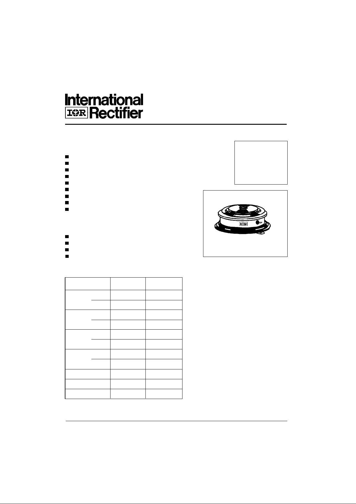
370A
INVERTER GRADE THYRISTORS Hockey Puk Version
ST183C..C SERIES
D-521
Bulletin I25178/A
Typical Applications
Inverters
Choppers
Induction heating
All types of force-commutated converters
Features
Metal case with ceramic insulator
International standard case TO-200AB (A-PUK)
All diffused design
Center amplifying gate
Guaranteed high dV/dt
Guaranteed high dI/dt
High surge current capability
Low thermal impedance
High speed performance
case style TO-200AB (A-PUK)
I
T(AV)
370 A
@ T
hs
55 °C
I
T(RMS)
690 A
@ T
hs
25 °C
I
TSM
@ 50Hz 4900 A
@ 60Hz 5130 A
I
2
t @ 50Hz 120 KA2s
@ 60Hz 110 KA
2
s
V
DRM/VRRM
400 to 800 V
t
q
range 10 to 20 µs
T
J
- 40 to 125 °C
Parameters ST183C..C Units
Major Ratings and Characteristics
Page 3
ST183C..C Series
D-522
ST183C..C 40
Voltage V
DRM/VRRM
, maximum V
RSM
, maximum I
DRM/IRRM
max.
Type number Code repetitive peak voltage non-repetitive peak voltage
@ TJ = TJ max.
V V mA
04 400 500
08 800 900
ELECTRICAL SPECIFICATIONS
Voltage Ratings
Frequency Units
50Hz 770 660 1220 1160 5450 4960
400Hz 730 600 1270 1090 2760 2420
1000Hz 600 490 1210 1040 1600 1370 A
2500Hz 350 270 860 730 800 680
Recovery voltage Vr 50 50 50 50 50 50
Voltage before turn-on Vd V
DRM
V
DRM
V
DRM
Rise of on-state current di/dt 50 50 - - - - A/µs
Heatsink temperature 40 55 40 55 40 55 °C
Equivalent values for RC circuit 47Ω / 0.22µF 47Ω / 0.22µF 47Ω / 0.22µF
I
TM
180oel
180
o
el
100µs
I
TM
I
TM
Current Carrying Capability
V
I
T(AV)
Max. average on-state current 370 (130) A 180° conduction, half sine wave
@ Heatsink temperature 55 (85) °C double side (single side) cooled
I
T(RMS)
Max. RMS on-state current 690 DC@ 25°C heatsink temperature double side cooled
I
TSM
Max. peak, one half cycle, 4900 t = 10ms No voltage
non-repetitive surge current 5130 A t = 8.3ms reapplied
4120 t = 10ms 100% V
RRM
4310 t = 8.3ms reapplied Sinusoidal half wave,
I
2
t Maximum I2t for fusing 120 t = 10ms No voltage Initial TJ = TJ max
110 t = 8.3ms reapplied
85 t = 10ms 100% V
RRM
78 t = 8.3ms reapplied
I
2
√t Maximum I2√t for fusing 1200 KA2√s t = 0.1 to 10ms, no voltage reapplied
Parameter ST183C..C Units Conditions
On-state Conduction
KA2s
Page 4

ST183C..C Series
D-526
Fig. 3 - Current Ratings Characteristics Fig. 4 - Current Ratings Characteristics
Fig. 5 - On-state Power Loss Characteristics Fig. 6 - On-state Power Loss Characteristics
Fig. 7 - Maximum Non-repetitive Surge Current
Single and Double Side Cooled
Fig. 8 - Maximum Non-repetitive Surge Current
Single and Double Side Cooled
Page 5

ST183C..C Series
D-527
Fig. 9 - On-state Voltage Drop Characteristics
Fig. 10 - Thermal Impedance Z
thJ-hs
Characteristics
Fig. 11 - Reverse Recovered Charge Characteristics Fig. 12 - Reverse Recovery Current Characteristics
Fig. 13 - Frequency Characteristics
Page 6

ST183C..C Series
D-528
Fig. 14 - Frequency Characteristics
Fig. 15 - Frequency Characteristics
Fig. 16 - Maximum On-state Energy Power Loss Characteristics
Page 7

ST183C..C Series
D-529
Fig. 17 - Gate Characteristics
Page 8

ST183C..C Series
D-523
VTMMax. peak on-state voltage 1.80 ITM= 600A, TJ = TJ max, tp = 10ms sine wave pulse
V
T(TO)1
Low level value of threshold
voltage
V
T(TO)2
High level value of threshold
voltage
r
t
1
Low level value of forward
slope resistance
r
t
2
High level value of forward
slope resistance
I
H
Maximum holding current 600 TJ = 25°C, IT > 30A
I
L
Typical latching current 1000 TJ = 25°C, VA= 12V, Ra = 6Ω, IG= 1A
Parameter ST183C..C Units Conditions
On-state Conduction
1.40 (16.7% x π x I
T(AV)
< I < π x I
T(AV)
), TJ = TJ max.
1.45 (I > π x I
T(AV)
), TJ = TJ max.
V
0.67 (16.7% x π x I
T(AV)
< I < π x I
T(AV)
), TJ = TJ max.
0.58 (I > π x I
T(AV)
), TJ = TJ max.
mΩ
mA
di/dt Max. non-repetitive rate of rise T
J
= TJ max, V
DRM
= rated V
DRM
of turned-on current I
TM
= 2 x di/dt
T
J
= 25°C, V
DM
= rated V
DRM, ITM
= 50A DC, tp= 1µs
Resistive load, Gate pulse: 10V, 5Ω source
T
J
= TJ max, I
TM
= 300A, commutating di/dt = 20A/µs
V
R
= 50V, tp = 500µs, dv/dt: see table in device code
Switching
Parameter ST183C..C Units Conditions
1000 A/µs
t
d
Typical delay time 1.1
Min Max
dv/dt Maximum critical rate of rise of T
J
= TJ max. linear to 80% V
DRM
, higher value
off-state voltage available on request
I
RRM
Max. peak reverse and off-state
I
DRM
leakage current
Parameter ST183C..C Units Conditions
Blocking
500 V/µs
40 mA T
J
= TJ max, rated V
DRM/VRRM
applied
PGMMaximum peak gate power 60
P
G(AV)
Maximum average gate power 10
I
GM
Max. peak positive gate current 10 A TJ = TJ max, tp ≤ 5ms
+V
GM
Maximum peak positive
gate voltage
-V
GM
Maximum peak negative
gate voltage
I
GT
Max. DC gate current required
to trigger
V
GT
Max. DC gate voltage required
to trigger
I
GD
Max. DC gate current not to trigger 20 mA
V
GD
Max. DC gate voltage not to trigger 0.25 V
Triggering
Parameter ST183C..C Units Conditions
20
5
V TJ = TJ max, tp ≤ 5ms
200 mA
3 V
T
J
= 25°C, VA = 12V, Ra = 6Ω
TJ = TJ max, rated V
DRM
applied
t
q
Max. turn-off time 10 20
µs
W TJ = TJ max, f = 50Hz, d% = 50
Page 9

ST183C..C Series
D-524
TJMax. operating temperature range -40 to 125
T
stg
Max. storage temperature range -40 to 150
R
thJ-hs
Max. thermal resistance, 0.17 DC operation single side cooled
junction to heatsink 0.08 DC operation double side cooled
R
thC-hs
Max. thermal resistance, 0.033 DC operation single side cooled
case to heatsink 0.017 DC operation double side cooled
F Mounting force, ± 10% 4900 N
(500) (Kg)
wt Approximate weight 50 g
Parameter ST183C..C Units Conditions
K/W
Thermal and Mechanical Specification
°C
Case style TO - 200AB (A-PUK) See Outline Table
K/W
Single Side Double Side Single Side Double Side
180° 0.015 0.016 0.011 0.011
120° 0.018 0.019 0.019 0.019
90° 0.024 0.024 0.026 0.026 K/W T
J
= TJ max.
60° 0.035 0.035 0.036 0.037
30° 0.060 0.060 0.060 0.061
Sinusoidal conduction Rectangular conduction
Conduction angle Units Conditions
∆R
thJ-hs
Conduction
(The following table shows the increment of thermal resistence R
thJ-hs
when devices operate at different conduction angles than DC)
Ordering Information Table
5
6
8
9
ST 18 3 C 08 C H K 1
3
4
10
7
Device Code
1 2
dv/dt - tq combinations available
dv/dt (V/µs) 20 50 100 200 400
10 CN DN EN FN* HN
12 CM DM EM FM HM
15 CL DL EL FL* HL
18 CP DP EP FP HP
20 CK DK EK FK HK
tq(µs)
*Standard part number.
All other types available only on request.
1 - Thyristor
2 - Essential part number
3 - 3 = Fast turn off
4 - C = Ceramic Puk
5 - Voltage code: Code x 100 = V
RRM
(See Voltage Rating Table)
6 - C = Puk Case TO-200AB (A-PUK)
7 - Reapplied dv/dt code (for t
q
test condition)
8 - t
q
code
9 - 0 = Eyelet term. (Gate and Aux. Cathode Unsoldered Leads)
1 = Fast-on term. (Gate and Aux. Cathode Unsoldered Leads)
2 = Eyelet term. (Gate and Aux. Cathode Soldered Leads)
3 = Fast-on term. (Gate and Aux. Cathode Soldered Leads)
- Critical dv/dt:
None = 500V/µsec (Standard value)
L = 1000V/µsec (Special selection)
10
Page 10

ST183C..C Series
D-525
Fig. 1 - Current Ratings Characteristics Fig. 2 - Current Ratings Characteristics
Case Style TO-200AB (A-PUK)
All dimensions in millimeters (inches)
Outline Table
DIA. MAX.
4.75 (0.19)
28 (1.10)
6.5 (0.26)
19 (0.75)
0.3 (0.01) MIN.
0.3 (0.01) MIN.
13.7 / 14.4
(0.54 / 0.57)
25°± 5°
GATE TERM. FOR
1.47 (0.06) DIA.
PIN RECEPTACLE
ANODE TO GATE
CREEPAGE DISTANCE: 7.62 (0.30) MIN.
STRIKE DISTANCE: 7.12 (0.28) MIN.
19 (0.75)
DIA. MAX.
38 (1.50) DIA MAX.
2 HOLES 3.56 (0.14) x
1.83 (0.07) MIN. DEEP
42 (1.65) MAX.
 Loading...