

Datasheet ST1284-03T8, ST1284-03A8, ST1284-02T8, ST1284-02A8, ST1284-01T8 Datasheet (SGS Thomson Microelectronics)
Page 1
1/7
ST1284-xxA8/T8
®
July 2002 - Ed: 1B
■
One device for parallel port termination
■
Compliant with IEEE1284 standard
■
EMI / RFI noise filtering
■
Highly integrated solution in 28 pin QSOP and
TSSOP packages
■ One single device provides the proper termina-
tion for 8 datalines, 1 strobe line, 4 control lines
and 4 statuts lines
■ In system ESD protection of ±15 kV (air dis-
charge) as per IEC61000-4-2 level 4
FEATURES
28
27
26
25
24
23
22
21
20
19
18
17
16
1514
13
12
11
10
9
8
7
6
5
4
3
2
1
Vcc Vcc VccVcc
Vcc
Vcc
Vcc
Vcc
Vcc
Vcc
Vcc
Vcc
Vcc
Gnd
Vcc
Vcc
Vcc
Vcc
Vcc
R1
C
R1CR1
R2
C
R1
R1
R1
R1
R1
R2
R1
R2
R1
R2
R1
R1
R2
C
Rs
C
Rs
C
Rs
C
Rs
C
Rs
C
Rs
C
Rs
C
Rs
Rs
C
C
C
C
C
C
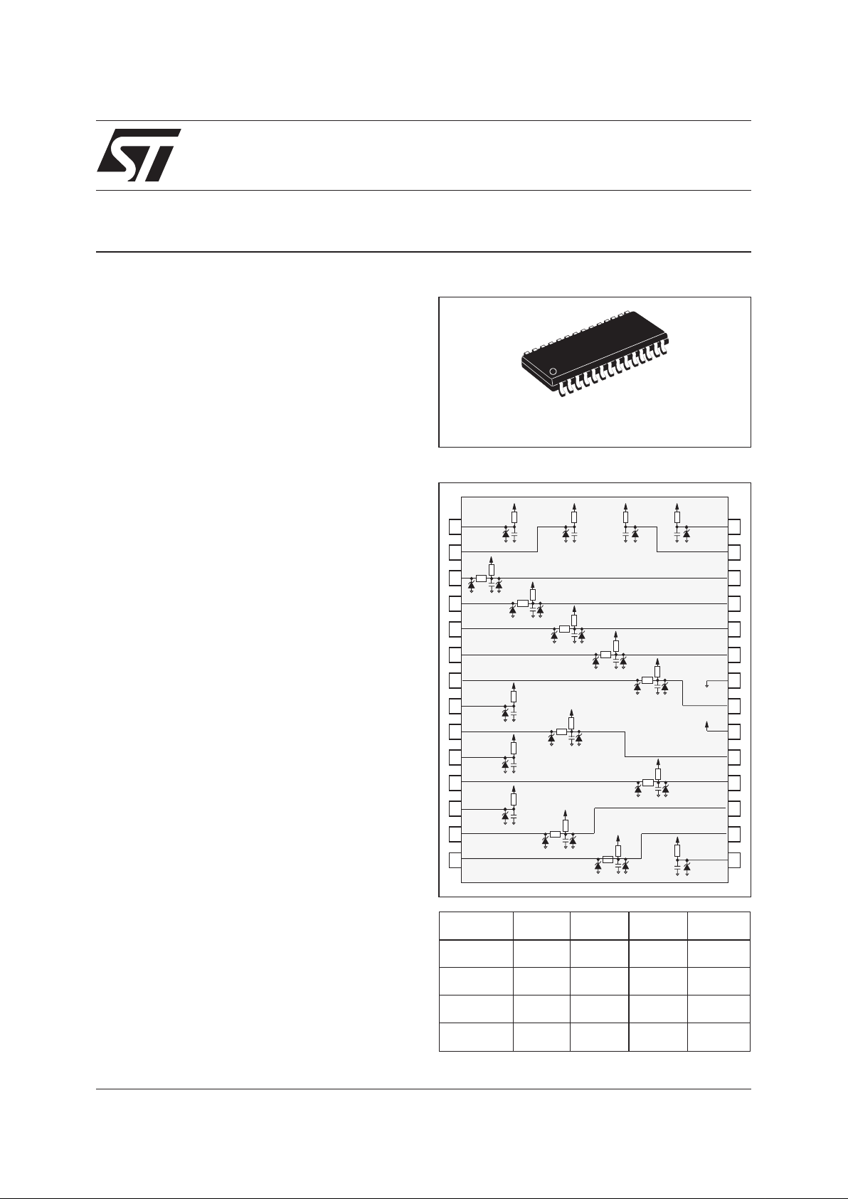
SCHEMATIC DIAGRAM
PARALLEL PORT SINGLE TERMINATION
NETWORK WITH ±15kV ESD PROTECTION
A.S.D.
TM
ECP/EPP Parallel Port termination on:
■
Desktops
■
Notebooks
■
Workstations
■
Servers
■
PC Peripherals
■
Set Top Box
MAIN APPLICATIONS
The ST1284-xxA8/T8 is a highly integrated termination forenhancedhigh speed parallel ports. The
integrated termination complies to the IEEE1284
Standard recommendations and government
EMC compatibility requirements. It is built around
two basic cells. The first one (Cell 1) provides line
termination, EMI filtering and ESD protection for
the Strobe and Datalines while the second one
(Cell 2) provides EMI filtering and ESD protection
for the Control and Status lines. In addition,
ST1284-xxA8 provides extra protection against
ESD. When tested according to IEC61000-4-2,
they withstand ±8kV contact discharges and
±15kV air-discharges, thereby providing to the
system the necessary robustness to meet up to
level 4of IEC61000-4-2, withoutthe need for additional ESD protection components. Cells 1 and 2
are described in more detail in figures 1 and 2.
DESCRIPTION
QSOP28 / TSSOP28
R1 R2
Rs
C
Code 01 4.7kΩ 4.7kΩ
33Ω
180pF
Code 02 2.2kΩ 2.2kΩ
33Ω
220pF
Code 03 1kΩ 5.1kΩ
39Ω
150pF
Tolerance ± 10% ± 10%
± 10%
± 20%
- IEC61000-4-2 ±15kV (airdischarge)
±8kV (contact discharge)
- MIL STD 883E - Method 3015-7 : Class 3
(human body model).
COMPLIES WITH THE FOLLOWING ESD
STANDARDS :
Page 2
ST1284-xxA8/T8
2/7
Symbol Parameter Value Unit
V
PP
ESD discharge IEC61000-4-2, air discharge
±16 kV
ESD discharge IEC61000-4-2, contact discharge
±9 kV
ESD discharge - MIL STD 883E - Method 3015-7
±25 kV
V
cc
Supply voltage
5.5 V
P
r
Power rating per resistor
100 mW
P
P
Package Power rating
1W
T
op
Operating temperature range
0 to +70 °C
T
stg
Storage temperature range
-55 to +150 °C
T
j
Maximum operating junction temperature
125 °C
ABSOLUTE MAXIMUM RATINGS (T
amb
25°C)
Symbol Parameter Test condition Min. Typ. Max. Unit
I
R
Leakage current
V
cc
= 5.0V 10 µA
V
BR
Breakdown voltage
I
R
= 1mA 6 V
V
F
Forward voltage drop
I
F
= 50mA 0.9 V
ELECTRICAL CHARACTERISTICS (T
amb
= 25°C)
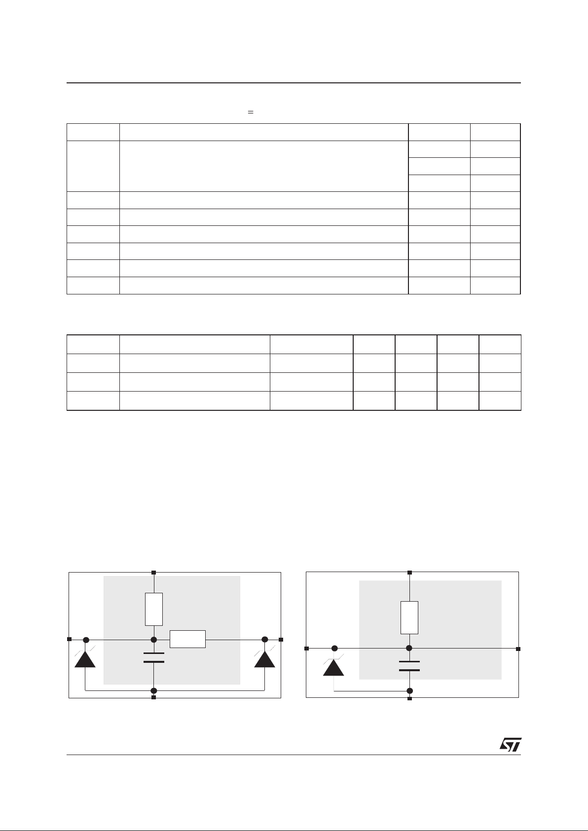
The ST1284-xxA8/T8 is built around the two basic cells described below which integrate the recommended IEEE1284 network and the ESD protection compatible with IEC61000-4-2 level 4
BASIC CELL CONFIGURATIONS
C
IEEE1284
Recommendation
Vcc
Gnd
Rp
Rs
Fig. 1:Cell 1 for line termination, EMI filtering and
ESD protection for the Datalines and Strobe signals. There are 9 of these cells inside the
ST1284-xxA8/T8
C
IEEE1284
Recommendation
Vcc
Gnd
Rp
Fig. 2: Cell 2 for EMI filtering and ESD protection
of the Control and Status signals. There are 8 of
these cells inside the ST1284-xxA8/T8
Page 3
3/7
ST1284-xxA8/T8
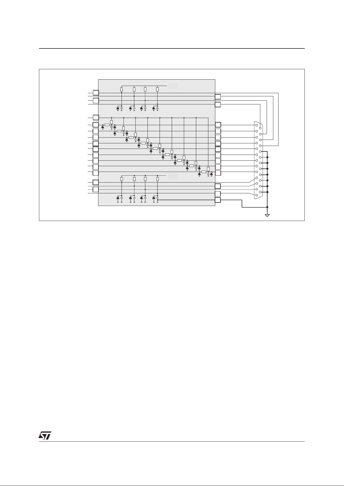
14 Autofeed
15 Error
16 Reset
17 Select in
1 Strobe
2 Bit 1
3 Bit 2
4 Bit 3
5 Bit 4
6 Bit 5
7 Bit 6
8 Bit 7
9 Bit 8
13 Select paper
14
1
13
25
1
28
2
27
20
26
25
24
23
21
19
18
17
16
3
4
5
6
7
9
11
13
14
8
10
12
15
22
10 Acknowledge
11 Busy
12 Paper Out
Vcc
Vcc
Vcc
Gnd
ST1284-xxA8/T8
FUNCTIONAL DIAGRAM
Thefunctional diagram here above presentsa IEEE1284-Aconnector pinoutand show how to connect
the ST1284-xxA8/T8in order to correctlyterminate and filter the17 signal lines. TheIEEE1284-A connector is the PC standard for the host connection.
Control and status lines (from 10 to 17) only require a pull-up resistor (Rp) and a filter capacitor (C).
The data lines (from 2 to 9) and the STROBE (pin 1) also require a termination series resistor (Rs)
in addition to the pull-up resistor and a filter capacitor. The Vcc is connected to pin 20 and the
ground to pin 22.
The ST1284-xxA8/T8 can be used with all 3 types of connectors defined in the IEEE1284 standard:
- IEEE1284-A is a 25DB connector which is the PC standard for the host connection.
- IEEE1284-B is a 36 pin, 0.085 inch centerline connector used on the peripheral device.
- IEEE1284-C is a new 36 pin, 0.050inch centerline connector which can beused for both host and peripherals.
APPLICATION INFORMATION
Page 4

4/7
ST1284-xxA8/T8
FREQUENCY BEHAVIOR OF DATA AND STROBE SIGNALS
TECHNICAL INFORMATION
ST1284
SPECTRUM
ANALYSER
TRACKING
GENERATOR
Vg
VoutVin
50
Ω
50
Ω
+5V
Fig. A1: Measurement conditions
1 3 10 30 100 300 1,000
-30.00
-25.00
-20.00
-15.00
-10.00
-5.00
0.00
dB
F (MHz)
1284 -01
1284 -02
1284 -03
Fig. A2: Typicalfrequency responsecurve fordata
and strobe signals.
Inaddition to therequirements of termination and EMCcompatibility, computing devices are requiredto be
tested for ESD susceptibility. This test is described in the IEC61000-4-2 and is already in place in Europe.
This test requires that a device tolerates ESD events and remain operational without user intervention.
The ST1284-xxA8/T8 is particularly optimized to perform ESD protection. ESD protection is based on the
use of device which clamps at :
Vouput V R I
BR d PP
=+.
This protection function is splitted in 2 stages. As shown in figure A3, the ESD strikes are clamped by the
first stage S1 and then its remaining overvoltage is applied to the second stage through the resistor R.
Such a configuration makes the voltage very low at the output.
ESD PROTECTION
ESD Surge
Vinput
Voutput
Rload
Rg
R
S1
Rd
V
BR
V
BR
V
PP
Device
to be
protected
ST1284-xxA8/T8
Rd
S2
Fig. A3: ST1284 ESD clamping behavior
Page 5

5/7
ST1284-xxA8/T8
To have a good approximation of the remaining voltages at both Vin and Vout stages, we give the typical
dynamical resistance value Rd. By taking into account these following hypothesis : Rt>Rd, Rg>Rd and
Rload>Rd, it gives these formulas:
Vinput
RV RV
R
gBR dPP
g
=
+..
Voutput
R V R Vinput
R
tBR d
t
=
+..
Theresults ofthe calculationdone forV
PP
=8kV,Rg=330Ω (IEC61000-4-2standard), VBR=7V(typ.)
and Rd = 1Ω (typ.) give:
Vinput = 31.2 V
Voutput = 7.95 V
This confirms the very low remaining voltage across the device to be protected.It is also important to note
that in this approximation the parasitic inductance effect was not taken into account. This could be few
tenths of volts during few ns at the input side. This parasitic effect is not present at the output side due the
low current involved after the resistance R.
The measurements done here after show very clearly (Fig. A5) the high efficiency of the ESD protection :
- no influence of the parasitic inductances on Vout stage
- Voutput clamping voltage very close to V
BR
(positive strike) and -VF(negative strike)
ST1284
Vinput Voutput
ESD
SURGE
Fig. A4: Measurement conditions
Fig. A5: Remaining voltage at the input and output of the device during a ±16kV ESD surge
(IEC61000-4-2).
Page 6

6/7
ST1284-xxA8/T8
PACKAGE MECHANICAL DATA
QSOP28 (Plastic)
REF.
DIMENSIONS
Millimeters Inches
Min. Max. Min. Max.
A 1.55 1.75 0.061 0.069
a1 0.10 0.25 0.004 0.010
b 0.20 0.30 0.008 0.012
b1 0.18 0.25 0.007 0.010
D 9.80 9.98 0.386 0.393
F 5.79 6.20 0.228 0.244
e 0.64 typ. 0.025 typ.
E 3.80 3.98 0.15 0.157
L 0.40 0.90 0.016 0.035
S 8°max 8° max
28 15
14
1
b
a1
e
S
L
E
F
D
b1
A
PACKAGE MECHANICAL DATA
TSSOP28 (Plastic)
28 15
14
1
b
A1
e
K
L
E1
E
D
c
A
A2
L1
aaa
REF.
DIMENSIONS
Millimeters Inches
Min. Typ. Max. Min. Typ. Max.
A 1.200 0.047
A1 0.050 0.150 0.002 0.006
A2 0.800 1.000 1.050 0.031 0.039 0.041
b 0.190 0.300 0.007 0.012
c 0.090 0.200 0.003 0.008
D 9.600 9.700 9.800 0.378 0.382 0.386
E 6.200 6.400 6.600 0.244 0.252 0.260
E1 4.300 4.400 4.500 0.169 0.173 0.177
e 0.650 0.026
L 0.450 0.600 0.750 0.018 0.024 0.029
L1 1.000 0.039
K0d 8d0d 8d
aaa 0.100 0.004
Page 7

ST1284-xxA8/T8
7/7
Informationfurnishedisbelievedtobeaccurateandreliable.However,STMicroelectronicsassumesnoresponsibilityfortheconsequencesof
useofsuch information nor for any infringement of patents or other rights of third parties which may result from its use. No license is grantedby
implication or otherwise under any patent or patent rights of STMicroelectronics. Specifications mentioned in this publication are subject to
change without notice. This publication supersedes and replaces all information previouslysupplied.
STMicroelectronics products are not authorized for use as critical components in life support devices or systems without express written approval of STMicroelectronics.
The ST logo is a registered trademark of STMicroelectronics
© 2002 STMicroelectronics - Printed in Italy - All rights reserved.
STMicroelectronics GROUP OF COMPANIES
Australia - Brazil - Canada - China - Finland - France - Germany
Hong Kong - India - Israel - Italy - Japan - Malaysia - Malta - Morocco - Singapore
Spain - Sweden - Switzerland - United Kingdom - United States.
http://www.st.com
Order code Marking Package Weight Delivery mode Base qty
ST1284-01A8 ST1284-01 QSOP28 0.147 g Tube 48
ST1284-01A8RL ST1284-01 QSOP28 0.147 g Tape & Reel 2500
ST1284-02A8 ST1284-02 QSOP28 0.147 g Tube 48
ST1284-02A8RL ST1284-02 QSOP28 0.147 g Tape & Reel 2500
ST1284-03A8RL ST1284-03 QSOP28 0.147 g Tape & Reel 2500
ST1284-01T8RL ST1284-01 TSSOP28 0.104g Tape & Reel 2500
ST1284-02T8RL ST1284-02 TSSOP28 0.104g Tape & Reel 2500
ST1284-03T8RL ST1284-03 TSSOP28 0.104g Tape & Reel 2500
dim in mm
0.4
7.1
3.7
0.65
1.7
FOOTPRINT (QSOP28 / TSSOP28)
Package General Specifications
Lead Plating Tin-Lead
Lead Plating
Thickness
7 µm Min
20 µm Max
Lead Material Copper Alloy
Lead Coplanarity 0.102 mm (0.004")
Body Material Molded Epoxy
Resine Meets UL94V.0 standard
 Loading...