

Page 1

6121 Baker Road,
Suite 108
Minnetonka, MN 55345
www.chtechnology.com
Phone (952) 933-6190
Fax (952) 933-6223
1-800-274-4284
Thank you for downloading this document from C&H Technology, Inc.
Please contact the C&H Technology team for the following questions -
Technical
Application
Assembly
Availability
Pricing
Phone – 1-800-274-4284
E-Mail – [email protected]
www.chtechnology.com - SPECIALISTS IN POWER ELECTRONIC COMPONENTS AND ASSEMBLIES - www.chtechnology.com
Page 2
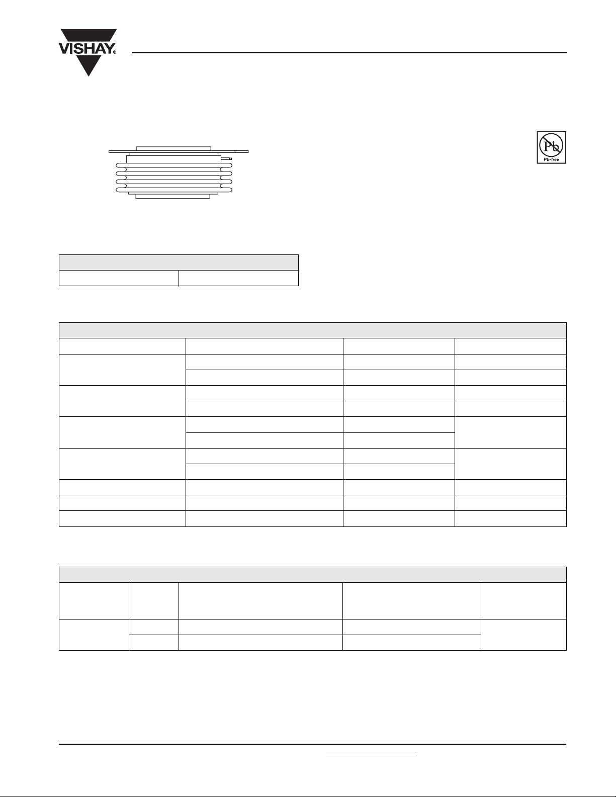
Vishay High Power Products
Phase Control Thyristors
(Hockey PUK Version), 2310 A
FEATURES
• Center amplifying gate
ST1280C..K Series
• Metal case with ceramic insulator
• International standard case A-24 (K-PUK)
• High profile hockey PUK
A-24 (K-PUK)
• Lead (Pb)-free
TYPICAL APPLICATIONS
PRODUCT SUMMARY
I
T(AV)
2310 A
• DC motor controls
• Controlled DC power supplies
• AC controllers
MAJOR RATINGS AND CHARACTERISTICS
PARAMETER TEST CONDITIONS VALUES UNITS
I
T(AV)
I
T(RMS)
I
TSM
2
I
t
V
DRM/VRRM
t
q
T
J
T
hs
T
hs
50 Hz 42 500
60 Hz 44 500
50 Hz 9027
60 Hz 8240
Typical 200 µs
2310 A
55 °C
4150 A
25 °C
A
kA2s
400 to 600 V
- 40 to 125 °C
RoHS
COMPLIANT
ELECTRICAL SPECIFICATIONS
VOLTAGE RATINGS
V
TYPE NUMBER
ST1280C..K
VOLTAGE
CODE
04 400 500
06 600 700
DRM/VRRM
, MAXIMUM REPETITIVE PEAK
AND OFF-STATE VOLTAGE
V
V
, MAXIMUM
NON-REPETITIVE PEAK VOLTAGE
RSM
V
I
DRM/IRRM
AT T
= TJ MAXIMUM
J
MAXIMUM
mA
100
www.vishay.com
Page 3
ST1280C..K Series
Vishay High Power Products
Phase Control Thyristors
(Hockey PUK Version),
2310 A
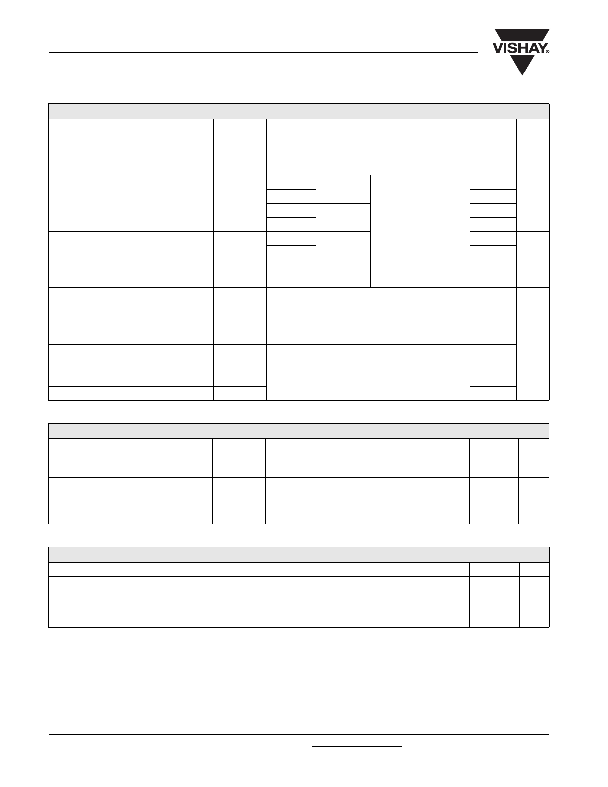
ON-STATE CONDUCTION
PARAMETER SYMBOL TEST CONDITIONS VALUES UNITS
Maximum average on-state current
at heatsink temperature
Maximum RMS on-state current I
I
T(RMS)
Maximum peak, one-cycle
non-repetitive surge current
2
Maximum I
Maximum I
t for fusing I2t
2
√t for fusing I2√t t = 0.1 to 10 ms, no voltage reapplied 90 270 kA2√s
Low level value of threshold voltage V
High level value of threshold voltage V
Low level value of on-state slope resistance r
High level value of on-state slope resistance r
Maximum on-state voltage V
Maximum holding current I
Typical latching current I
T(AV)
180° conduction, half sine wave
Double side (single side) cooled
25 °C heatsink temperature double side cooled 4150
I
TSM
T(TO)1
T(TO)2
t1
t2
TM
H
L
t = 10 ms
t = 8.3 ms 44 500
t = 10 ms
t = 8.3 ms 37 400
t = 10 ms
t = 8.3 ms 8241
t = 10 ms
t = 8.3 ms 5828
(16.7 % x π x I
(I > π x I
(16.7 % x π x I
(I > π x I
Ipk = 8000 A, TJ = TJ maximum, tp = 10 ms sine pulse 1.44 V
TJ = 25 °C, anode supply 12 V resistive load
No voltage
reapplied
100 % V
reapplied
No voltage
RRM
Sinusoidal half wave,
initial T
= TJ maximum
J
reapplied
100 % V
RRM
reapplied
< I < π x I
T(AV)
), TJ = TJ maximum 0.90
T(AV)
< I < π x I
T(AV)
), TJ = TJ maximum 0.068
T(AV)
), TJ = TJ maximum 0.83
T(AV)
), TJ = TJ maximum 0.077
T(AV)
2310 (885) A
55 (85) °C
42 500
35 700
9027
6383
600
1000
A
kA2s
V
mΩ
mA
SWITCHING
PARAMETER SYMBOL TEST CONDITIONS VALUES UNITS
Maximum non-repetitive rate of
rise of turned-on current
Typical delay time t
Typical turn-off time t
dI/dt
d
q
Gate drive 20 V, 20 Ω, t
T
= TJ maximum, anode voltage ≤ 80 % V
J
≤ 1 µs
r
DRM
Gate current 1 A, dIg/dt = 1 A/µs
V
= 0.67 % V
d
, TJ = 25 °C
DRM
ITM = 550 A, TJ = TJ maximum, dI/dt = 40 A/µs,
V
= 50 V, dV/dt = 20 V/µs, gate 0 V 100 Ω, tp = 500 µs
R
1000 A/µs
1.9
µs
200
BLOCKING
PARAMETER SYMBOL TEST CONDITIONS VALUES UNITS
Maximum critical rate of rise of
off-state voltage
Maximum peak reverse and
off-state leakage current
dV/dt T
,
I
RRM
I
DRM
= TJ maximum linear to 80 % rated V
J
TJ = TJ maximum, rated V
DRM/VRRM
DRM
500 V/µs
applied 100 mA
www.vishay.com For technical questions, contact: [email protected]
Document Number: 93718
2 Revision: 15-May-08
Page 4
ST1280C..K Series
Phase Control Thyristors
Vishay High Power Products
(Hockey PUK Version),
2310 A
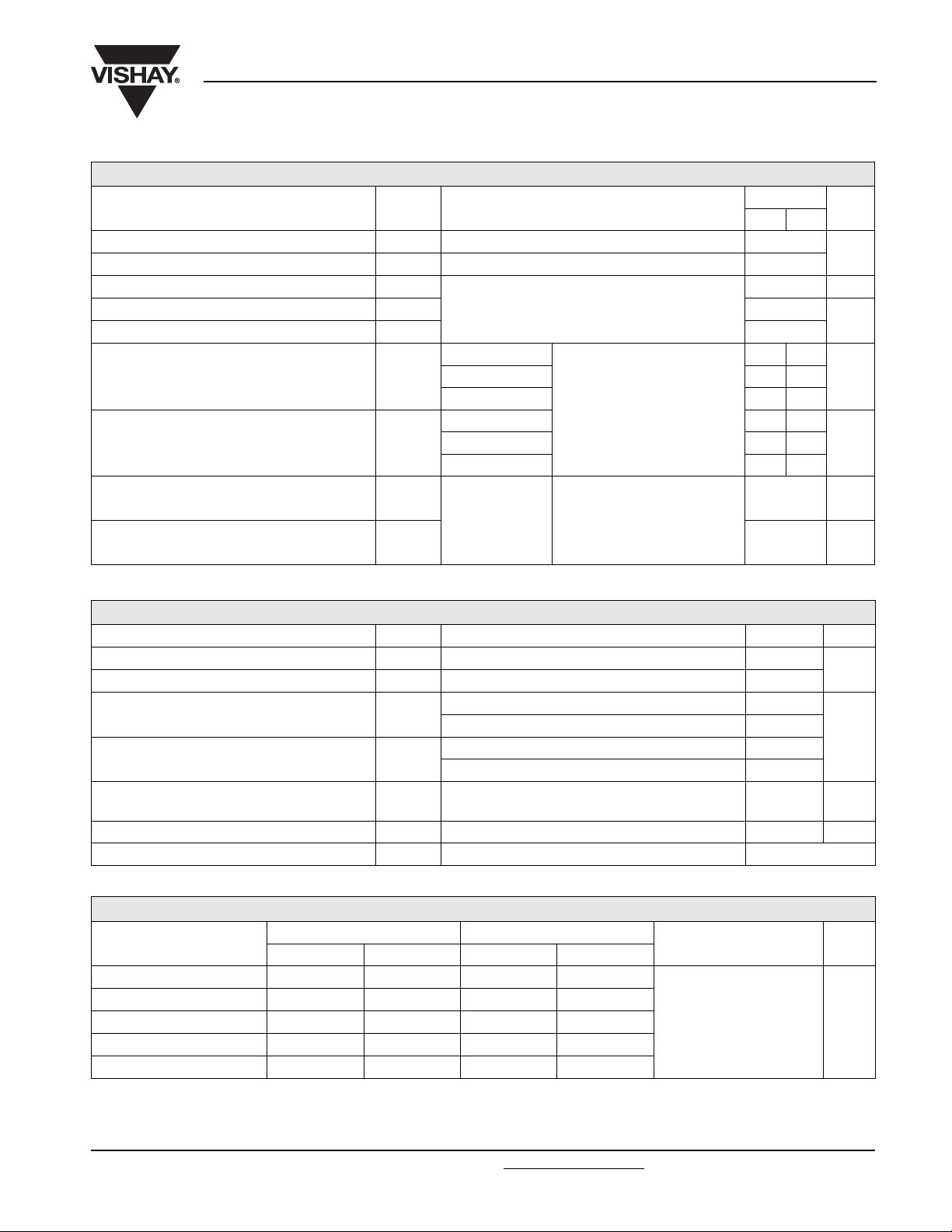
TRIGGERING
PARAMETER SYMBOL TEST CONDITIONS
Maximum peak gate power P
Maximum average gate power P
Maximum peak positive gate current I
Maximum peak positive gate voltage + V
Maximum peak negative gate voltage - V
GM
G(AV)
GM
TJ = TJ maximum, tp ≤ 5 ms 16
TJ = TJ maximum, f = 50 Hz, d% = 50 3
TJ = TJ maximum, tp ≤ 5 ms
GM
GM
TJ = - 40 °C
DC gate current required to trigger I
DC gate voltage required to trigger V
DC gate current not to trigger I
DC gate voltage not to trigger V
GT
GT
GD
GD
= 25 °C 100 200
J
T
= 125 °C 50 -
J
TJ = - 40 °C 1.4 -
= 25 °C 1.1 3.0
T
J
= 125 °C 0.9 -
T
J
Maximum required gate trigger/
current/voltage are the lowest
value which will trigger all units
12 V anode to cathode applied
Maximum gate current/voltage
not to trigger is the maximum
TJ = TJ maximum
value which will not trigger any
unit with rated V
anode to
DRM
cathode applied
VALUES
TYP. MAX.
3.0 A
20
5.0
200 -
10 mA
0.25 V
UNITS
W
V
mAT
V
THERMAL AND MECHANICAL SPECIFICATIONS
PARAMETER SYMBOL TEST CONDITIONS VALUES UNITS
Maximum operating temperature range T
Maximum storage temperature range T
Maximum thermal resistance, junction to heatsink R
Maximum thermal resistance, case to heatsink R
J
Stg
thJ-hs
thC-hs
DC operation single side cooled 0.042
DC operation double side cooled 0.021
DC operation single side cooled 0.006
DC operation double side cooled 0.003
Mounting force, ± 10 %
Approximate weight 425 g
Case style See dimensions - link at the end of datasheet A-24 (K-PUK)
ΔR
CONDUCTION
thJC
CONDUCTION ANGLE
SINUSOIDAL CONDUCTION RECTANGULAR CONDUCTION
SINGLE SIDE DOUBLE SIDE SINGLE SIDE DOUBLE SIDE
TEST CONDITIONS UNITS
180° 0.003 0.003 0.002 0.002
120° 0.004 0.004 0.004 0.004
90° 0.005 0.005 0.005 0.005
= TJ maximum K/W
T
J
60° 0.007 0.007 0.007 0.007
30° 0.012 0.012 0.012 0.012
Note
• The table above shows the increment of thermal resistance R
when devices operate at different conduction angles than DC
thJC
- 40 to 125
- 40 to 150
24 500
(2500)
°C
K/W
N
(kg)
Document Number: 93718 For technical questions, contact: [email protected]
www.vishay.com
Revision: 15-May-08 3
Page 5
ST1280C..K Series
Vishay High Power Products
130
120
110
100
90
80
70
60
50
40
0 400 800 1200 1600
Maximum Allowable Heatsink Temperature (°C)
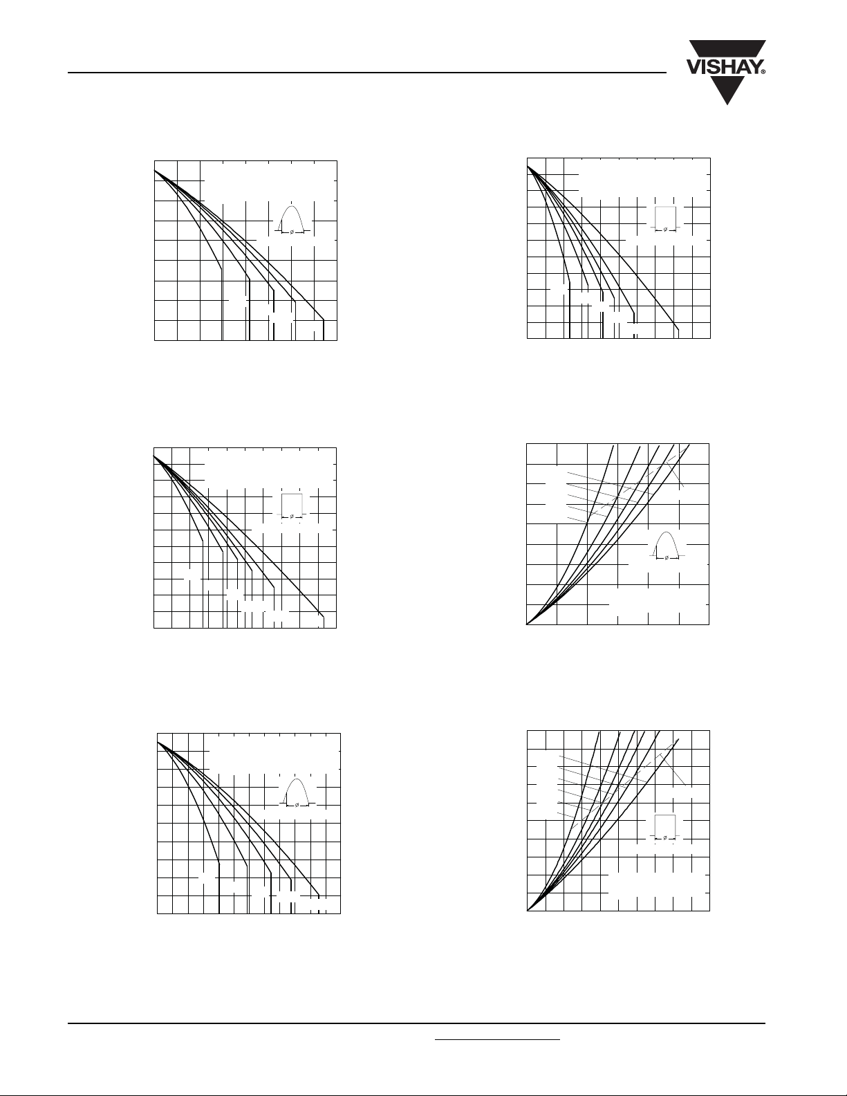
Fig. 1 - Current Ratings Characteristics
130
120
110
100
90
80
70
60
50
40
30
20
0 500 1000 1500 2000 2500
Maximum Allowable Heatsink Temperature (°C)
Fig. 2 - Current Ratings Characteristics
ST1280C..K Series
(Single Side Cooled)
R (DC) = 0.042 K/W
thJ-hs
Conduction Angle
30˚
60˚
90˚
120˚
180˚
Average On-state current (A)
ST1280C..K Series
(Single Side Cooled)
R (DC) = 0.042 K/W
thJ-hs
Conduction Period
30˚
60˚
90˚
120˚
180˚
Average On-state current (A)
Phase Control Thyristors
(Hockey PUK Version),
2310 A
DC
130
120
110
ST1280C..K Series
(Double Side Cooled)
R (DC) = 0.021 K/W
thJ-hs
100
90
80
Conduction Period
70
60
30˚
50
40
30
20
0 1000 2000 3000 4000 5000
Maximum Allowable Heatsink Temperature (°C)
60˚
90˚
120˚
180˚
DC
Average On-state Current (A)
Fig. 4 - Current Ratings Characteristics
3600
3200
2800
2400
2000
180˚
120˚
90˚
60˚
30˚
RMS Limit
1600
1200
800
400
Conduction Angle
ST1280C..K Series
T = 125˚C
J
0
0 500 1000 1500 2000 2500 3000
Maximum Average On-state Power Loss (W)
Average On-state Current (A)
Fig. 5 - On-State Power Loss Characteristics
130
120
110
ST1280C..K Series
(Double Side Cooled)
R (DC) = 0.021 K/W
thJ-hs
100
90
80
Conduction Angle
70
60
50
40
30˚
60˚
90˚
30
0 500 1000 1500 2000 2500 3000
Maximum Allowable Heatsink Temperature (°C)
Average On-state Current (A)
Fig. 3 - Current Ratings Characteristics
120˚
180˚
5000
4500
4000
3500
3000
2500
2000
1500
1000
Maximum Average On-state Power Loss (W)
DC
180˚
120˚
90˚
60˚
30˚
ST1280C..K Series
500
0
0 1000 2000 3000 4000 5000
T = 125˚C
J
RMS Limit
Conduction Period
Average On-state Current (A)
Fig. 6 - On-State Power Loss Characteristics
www.vishay.com For technical questions, contact: [email protected]
Document Number: 93718
4 Revision: 15-May-08
Page 6
ST1280C..K Series
Phase Control Thyristors
(Hockey PUK Version),
40000
35000
30000
25000
20000
15000
Peak Half Sine Wave On-state Current (A)
At Any Rated Load Condition And With
Rated V Applied Following Surge.
RRM
ST1280C..K Series
Initial T = 125˚C
J
@ 60 Hz 0.0083 s
@ 50 Hz 0.0100 s
110100
Number Of Equal Amplitude Half Cycle Current Pulses (N)
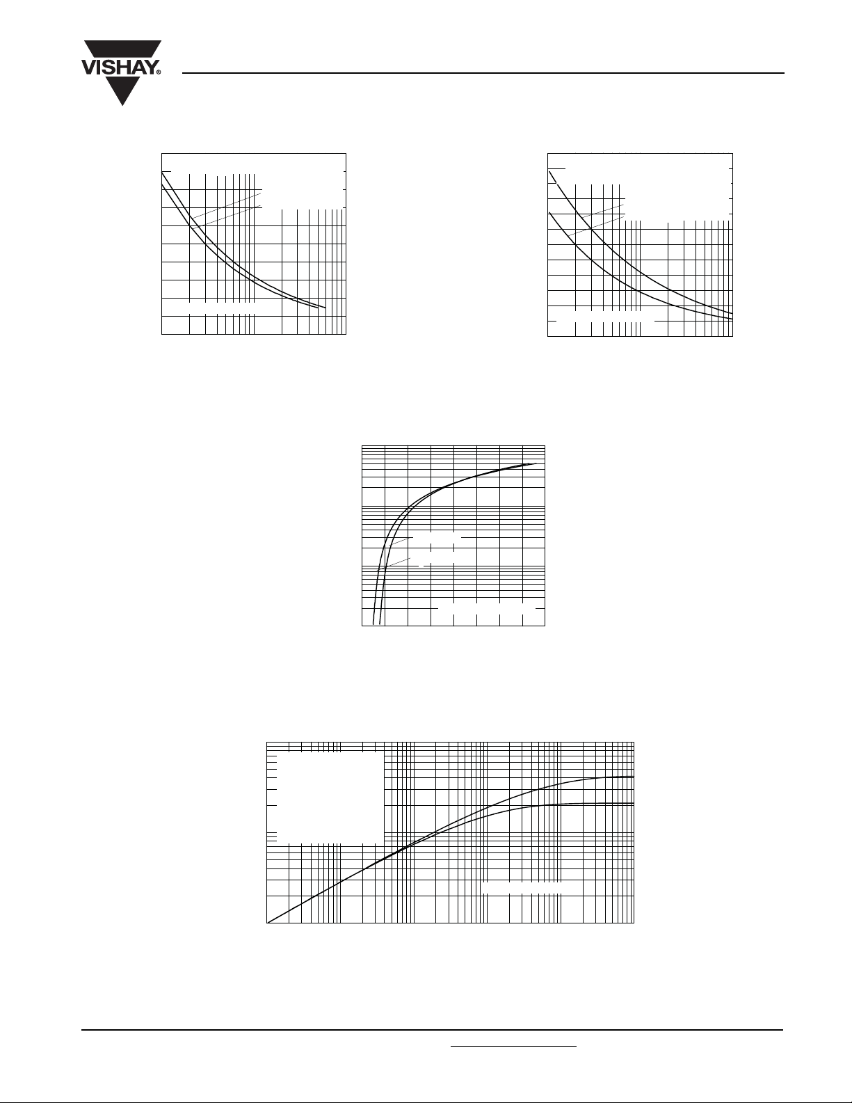
Fig. 7 - Maximum Non-Repetitive Surge Current
Single and Double Side Cooled
100000
2310 A
Vishay High Power Products
45000
Maximum Non Repetitive Surge Current
Versus Pulse Train Duration. Control
40000
35000
30000
25000
20000
15000
Peak Half Sine Wave On-state Current (A)
Of Conduction May Not Be Maintained.
ST1280C..K Series
Initial T = 125 ˚C
No Voltage Reapplied
Rated V Reapplied
J
RRM
0.01 0.1 1
Pulse Train Duration (s)
Fig. 8 - Maximum Non-Repetitive Surge Current
Single and Double Side Cooled
0.1
thJ-hs
0.01
10000
1000
Instantaneous On-state Current (A)
100
0.5 1 1.5 2 2.5 3 3.5 4 4.5
Fig. 9 - On-State Voltage Drop Characteristics
Steady State Value
R = 0.042 K/W
thJ-hs
(Single Side Cooled)
R = 0.021 K/W
thJ-hs
(Double Side Cooled)
(DC Operation)
T = 25˚C
J
T = 125˚C
J
ST1280C..K Series
Instantaneous On-state Voltage (V)
ST1280C..K Series
0.001
Transient Thermal Impedance Z (K/W)
0.001 0.01 0.1 1 10 100
Square Wave Pulse Duration (s)
Fig. 10 - Thermal Impedance Z
Characteristics
thJ-hs
Document Number: 93718 For technical questions, contact: [email protected]
www.vishay.com
Revision: 15-May-08 5
Page 7
ST1280C..K Series
(b)
(a)
(1)
Vishay High Power Products
100
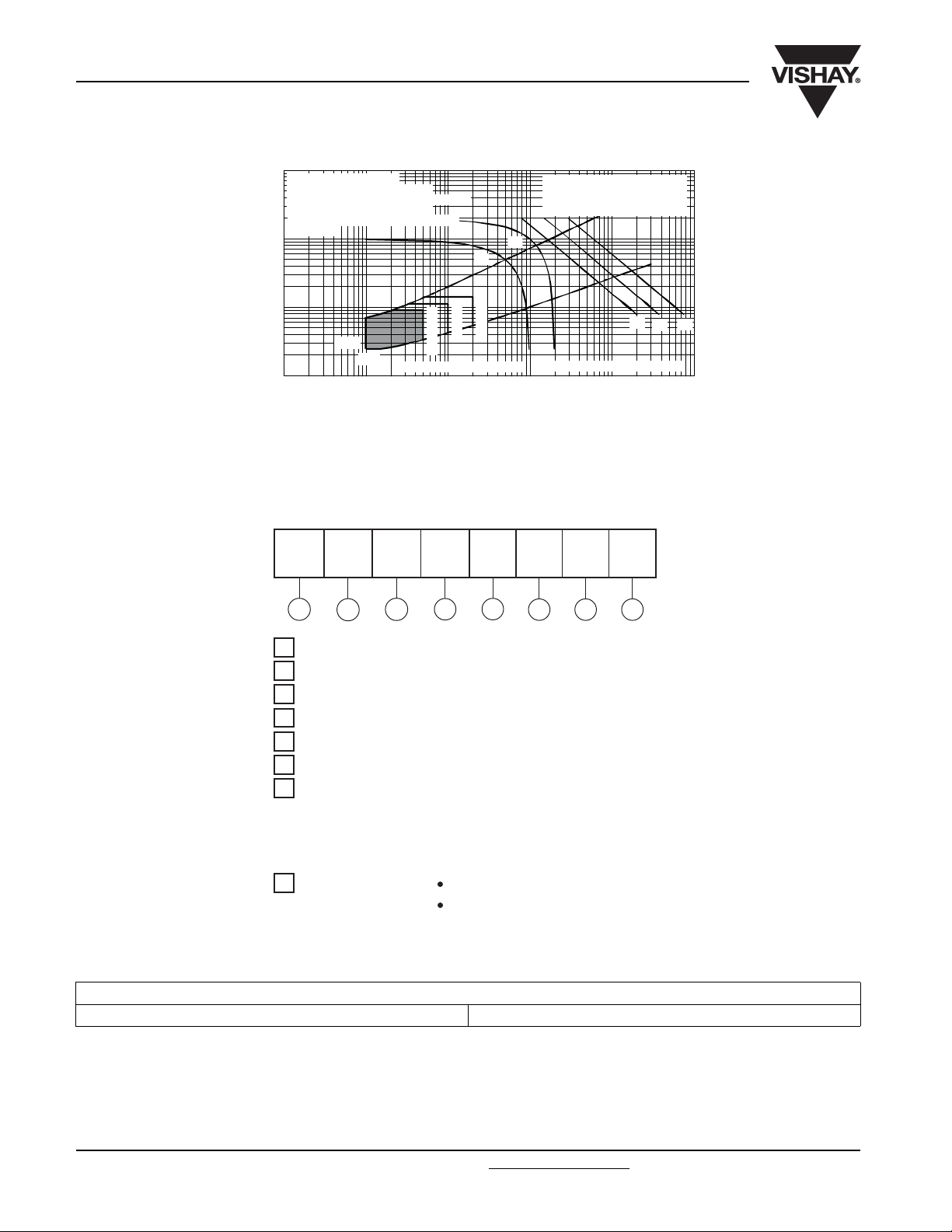
Rectangulargate pulse
a) Recommended load line for
rated di/dt : 20V, 10ohms; tr<=1 µs
b) Recommended load line for
<=30% rated di/dt : 10V, 10ohms
tr<=1 µs
10
1
Instantaneous Gate Voltage (V)
0.1
0.001 0.01 0.1 1 10 100
ORDERING INFORMATION TABLE
VG D
Phase Control Thyristors
(Hockey PUK Version),
2310 A
Tj=-40 °C
Tj=25 °
Tj=125 °C
C
IG D
Device: ST1280C..K Series
Instantaneous Gate Current (A)
Fig. 11 - Gate Characteristics
Frequency Limited by PG(AV)
(1) PGM = 16W, tp = 4ms
(2) PGM = 30W, tp = 2ms
(3) PGM = 60W, tp = 1ms
(2) (3)
Device code
ST 128 0 C 06 K 1 -
51324678
1 - Thyristor
2 - Essential part number
3 - 0 = Converter grade
4
- C = Ceramic PUK
5
- Voltage code x 100 = V
6
- K = PUK case A-24 (K-PUK)
7
- 0 = Eyelet terminals (gate and auxiliary cathode unsoldered leads)
(see Voltage Ratings table)
RRM
1 = Fast-on terminals (gate and auxiliary cathode unsoldered leads)
2 = Eyelet terminals (gate and auxiliary cathode soldered leads)
3 = Fast-on terminals (gate and auxiliary cathode soldered leads)
8 - Critical dV/dt:
None = 500 V/µs (standard selection)
L = 1000 V/µs (special selection)
LINKS TO RELATED DOCUMENTS
Dimensions http://www.vishay.com/doc?95081
Document Number: 93718
Page 8
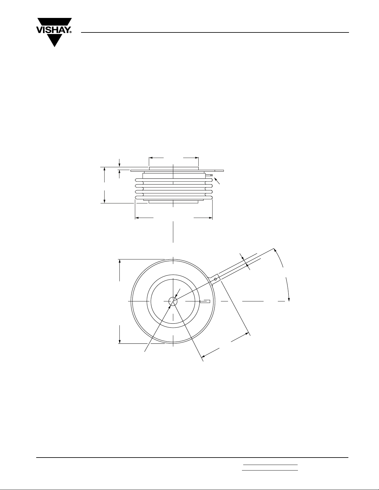
DIMENSIONS in millimeters (inches)
Outline Dimensions
Vishay High Power Products
A-24 (K-PUK)
Case Style A-24 (K-PUK)
Creepage distance: 28.88 (1.137) minimum
Strike distance: 17.99 (0.708) minimum
1 (0.04) MIN.
2 places
27.5 (1.08) MAX.
47.5 (1.87) DIA. MAX.
2 places
67 (2.6) DIA. MAX.
74.5 (2.9) DIA. MAX.
Pin receptable
AMP. 60598-1
4.75 (0.2) NOM.
20° ± 5°
44 (1.73)
2 holes DIA. 3.5 (0.14) x 2.1 (0.1) deep
Quote between upper and lower pole pieces has to be considered after
application of mounting force (see thermal and mechanical specification)
Document Number: 95081 For technical questions concerning discrete products, contact: [email protected]
Revision: 02-Aug-07 For technical questions concerning module products, contact: [email protected]
www.vishay.com
1
 Loading...