

Datasheet ST110S16P2L, ST110S16P2, ST110S16P1L, ST110S16P1, ST110S16P0L Datasheet (International Rectifier)
...Page 1
Features
Center gate
Hermetic metal case with ceramic insulator
(Also available with glass-metal seal up to 1200V)
International standard case TO-209AC (TO-94)
Threaded studs UNF 1/2 - 20UNF2A
Compression Bonded Encapsulation for heavy duty
operations such as severe thermal cycling
Typical Applications
DC motor controls
Controlled DC power supplies
AC controllers
I
T(AV)
110 A
@ T
C
90 °C
I
T(RMS)
175 A
I
TSM
@ 50Hz 2700 A
@ 60Hz 2830 A
I2t@
50Hz 36.4 KA2s
@ 60Hz 33.2 KA2s
V
DRM/VRRM
400 to 1600 V
t
q
typical 100 µs
T
J
- 40 to 125 °C
Parameters ST110S Units
Major Ratings and Characteristics
case style
TO-209AC (TO-94)
110A
PHASE CONTROL THYRISTORS Stud Version
ST110S SERIES
Bulletin I25167/B
Page 2
ST110S Series
ELECTRICAL SPECIFICATIONS
Voltage Ratings
Voltage V
DRM/VRRM
, max. repetitive V
RSM
, maximum non- I
DRM/IRRM
max.
Type number Code peak and off-state voltage repetitive peak voltage @ T
J
= TJ max
VVmA
04 400 500
08 800 900
ST110S 12 1200 1300 20
14 1400 1500
16 1600 1700
I
T(AV)
Max. average on-state current 110 A 180° conduction, half sine wave
@ Case temperature 90 °C
I
T(RMS)
Max. RMS on-state current 175 A DC @ 85°C case temperature
I
TSM
Max. peak, one-cycle 2700 t = 10ms No voltage
non-repetitive surge current 2830 t = 8.3ms reapplied
2270 t = 10ms 100% V
RRM
2380 t = 8.3ms reapplied Sinusoidal half wave,
I
2
t Maximum I2t for fusing 36.4 t = 10ms No voltage Initial TJ = TJ max.
33.2 t = 8.3ms reapplied
25.8 t = 10ms 100% V
RRM
23.5 t = 8.3ms reapplied
I
2
√t Maximum I2√t for fusing 364 KA2√s t = 0.1 to 10ms, no voltage reapplied
V
T(TO)1
Low level value of threshold
voltage
V
T(TO)
2
High level value of threshold
voltage
r
t1
Low level value of on-state
slope resistance
r
t2
High level value of on-state
slope resistance
V
TM
Max. on-state voltage 1.52 V Ipk= 350A, TJ = TJ max, tp = 10ms sine pulse
I
H
Maximum holding current 600
I
L
Typical latching current 1000
0.90 (16.7% x π x I
T(AV)
< I < π x I
T(AV)
), TJ = TJ max.
1.79 (16.7% x π x I
T(AV)
< I < π x I
T(AV)
), TJ = TJ max.
1.81 (I > π x I
T(AV)
),TJ = TJ max.
Parameter ST110S Units Conditions
0.92 (I > π x I
T(AV)
),TJ = TJ max.
On-state Conduction
KA2s
V
mΩ
mA
T
J
= 25°C, anode supply 12V resistive load
A
di/dt Max. non-repetitive rate of rise Gate drive 20V, 20Ω, tr ≤ 1µs
of turned-on current T
J
= TJ max, anode voltage ≤ 80% V
DRM
Gate current 1A, d ig/dt = 1A/µs
V
d
= 0.67% V
DRM, TJ
= 25°C
I
TM
= 100A, TJ = TJ max, di/dt = 10A/µs, VR = 50V
dv/dt
= 20V/µs, Gate 0V 100Ω, tp = 500µs
Parameter ST110S Units Conditions
t
d
Typical delay time 2.0
Switching
t
q
Typical turn-off time 100
µs
500 A/µs
Page 3
ST110S Series
dv/dt Maximum critical rate of rise of
off-state voltage
I
RRM
Max. peak reverse and off-state
I
DRM
leakage current
Blocking
500 V/µs TJ = TJ max. linear to 80% rated V
DRM
Parameter ST110S Units Conditions
20 mA TJ = TJ max, rated V
DRM/VRRM
applied
T
J
Max. operating temperature range -40 to 125
T
stg
Max. storage temperature range -40 to 150
R
thJC
Max. thermal resistance,
junction to case
R
thCS
Max. thermal resistance,
case to heatsink
T Mounting torque, ± 10% 15.5 Non lubricated threads
(137)
14 Lubricated threads
(120)
wt Approximate weight 130 g
Parameter ST110S Units Conditions
0.195 DC operation
0.08 Mounting surface, smooth, flat and greased
Thermal and Mechanical Specification
P
GM
Maximum peak gate power 5 TJ = TJ max, tp ≤ 5ms
P
G(AV)
Maximum average gate power 1 TJ = TJ max, f = 50Hz, d% = 50
I
GM
Max. peak positive gate current 2.0 A TJ = TJ max, tp ≤ 5ms
+V
GM
Maximum peak positive
gate voltage
-V
GM
Maximum peak negative
gate voltage
I
GT
DC gate current required TJ = - 40°C
to trigger mA T
J
= 25°C
TJ = 125°C
V
GT
DC gate voltage required TJ = - 40°C
to trigger V TJ = 25°C
T
J
= 125°C
I
GD
DC gate current not to trigger 10 mA
Parameter ST110S Units Conditions
20
5.0
Triggering
V
GD
DC gate voltage not to trigger 0.25 V
T
J
= TJ max
TYP. MAX.
180 -
90 150
40 -
2.9 -
1.8 3.0
1.2 Max. gate current/ voltage not to
trigger is the max. value which
will not trigger any unit with rated
V
DRM
anode-to-cathode applied
Max. required gate trigger/ current/ voltage are the lowest value
which will trigger all units 12V
anode-to-cathode applied
W
°C
K/W
Nm
(lbf-in)
Case style TO - 209AC (TO-94) See Outline Table
VT
J
= TJ max, tp ≤ 5ms
Page 4

ST110S Series
Ordering Information Table
5
3 4
ST 11 0 S 16 P 0 V
7
6
89
∆R
thJC
Conduction
(The following table shows the increment of thermal resistence R
thJC
when devices operate at different conduction angles than DC)
Device Code
12
180° 0.035 0.025 TJ = TJ max.
120° 0.041 0.042
90° 0.052 0.056 K/ W
60° 0.076 0.079
30° 0.126 0.127
Conduction angle Sinusoidal conduction Rectangular conduction Units Conditions
1 - Thyristor
2 - Essential part number
3 - 0 = Converter grade
4 - S = Compression bonding Stud
5 - Voltage code: Code x 100 = V
RRM
(See Voltage Rating Table)
6 - P = Stud base 20UNF threads
7 - 0 = Eyelet terminals (Gate and Auxiliary Cathode Leads)
1 = Fast - on terminals (Gate and Auxiliary Cathode Leads)
2 = Flag terminals (For Cathode and Gate Terminals)
8 - V = Glass-metal seal (only up to 1200V)
None = Ceramic housing (over 1200V)
9 - Critical dv/dt: None = 500V/µsec (Standard value)
L = 1000V/µsec (Special selection)
Page 5

ST110S Series
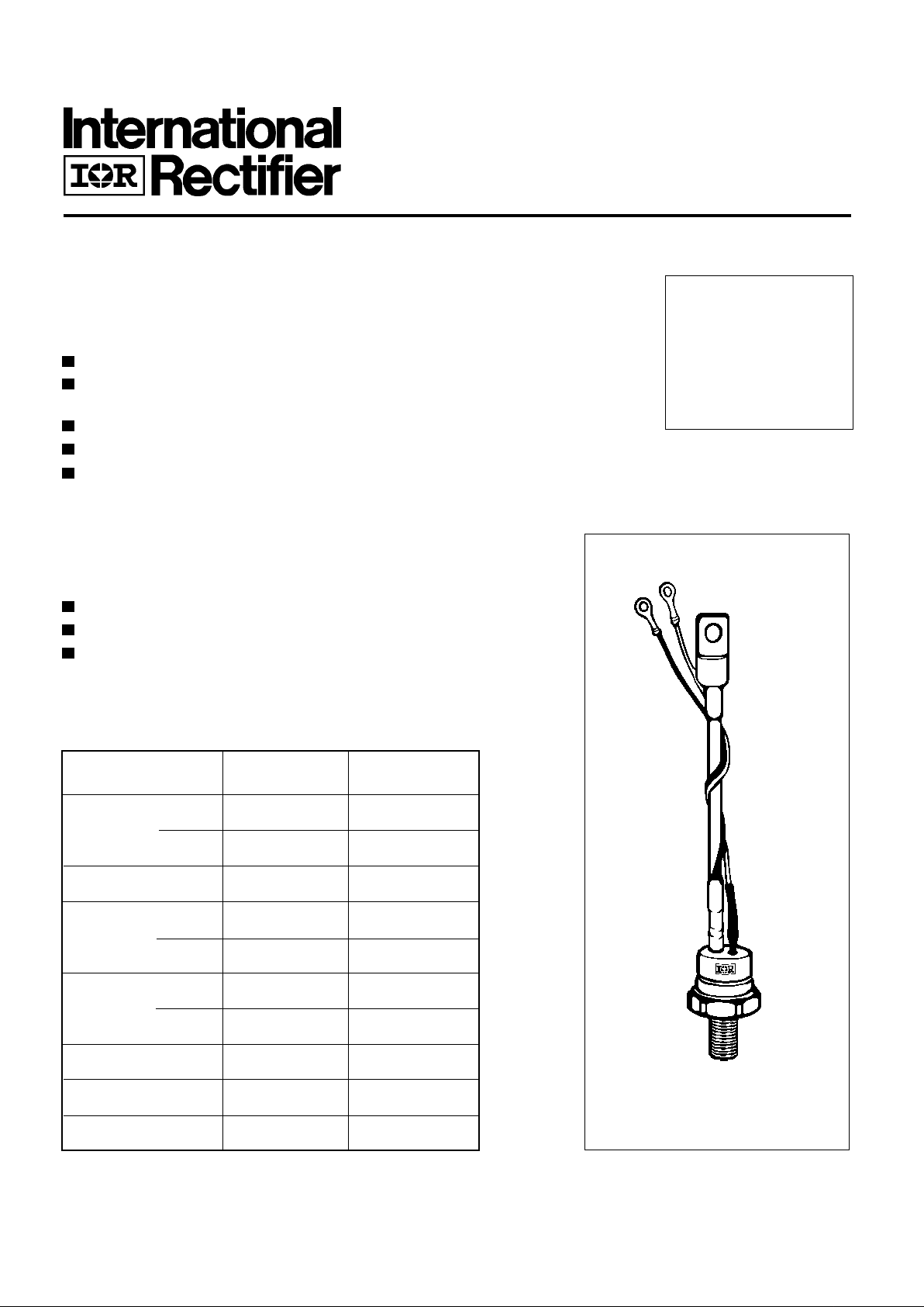
Fast-on Terminals
Case Style TO-209AC (TO-94)
All dimensions in millimeters (inches)
Outline Table
C.S. 0.4 mm
2
10 (0.39)
RED SHRINK
RED CATHODE
RED SILICON RUBBER
4.3 (0.17) DIA
21 (0.83)
12.5 (0.49) MAX.
157 (6.18)
170 (6.69)
(.0006 s.i.)
8.5 (0.33) DIA.
16.5 (0.65) MAX.
MAX.
70 (2.75) MIN.
CERAMIC HOUSING
22.5 (0.88) MAX. DIA.
29 (1.14) MAX.
SW 27
C.S. 16mm
2
FLEXIBLE LEAD
(.025 s.i.)
2.6 (0.10) MAX.
WHITE SHRINK
2
0
(
0
.
7
9
)
M
I
N
.
29.5 (1.16)
MAX.
1/2"-20UNF-2A
9
.
5
(
0
.
3
7
)
M
I
N
.
WHITE GATE
215 (8.46)
C.S. 0.4 mm
2
215 (8.46) 10 (0.39)
WHITE SHRINK
RED SHRINK
RED CATHODE
RED SILICON RUBBER
4.3 (0.17) DIA
21 (0.83)
12.5 (0.49) MAX.
157 (6.18)
170 (6.69)
(.0006 s.i.)
GLASS METAL SEAL
8.5 (0.33) DIA.
16.5 (0.65) MAX.
23.5 (0.93) MAX. DIA.
MAX.
29 (1.14) MAX.
70 (2.75) MIN.
C.S. 16mm
2
FLEXIBLE LEAD
(.025 s.i.)
2.6 (0.10) MAX.
2
0
(
0
.
7
9
)
M
I
N
.
29.5 (1.16) MAX.
1/2"-20UNF-2A
SW 27
9
.
5
(
0
.
3
7
)
M
I
N
.
WHITE GATE
AMP. 280000-1
REF-250
Page 6

ST110S Series
Case Style TO-208AD (TO-83)
All dimensions in millimeters (inches)
Outline Table
10
1/2"-20UNF-2A
29.5 (1.16)
MAX.
MAX.
46 (1.81)
10
7.5
(0.30)
22.5 DIA.
16.5
(0.65)
12.5 (0.49)
5.2 (0.20) DIA.
29 (1 .14 )
(0.39)
(0.89) MAX.
21(0.83)
1.5 (0.06) DIA.
(0.39)
49 (1.93)
MAX.
CERAMIC HOUSING
FLAG TERMINALS
SW 27
2.4 (0.09)
10
1/2"-20UNF-2A
29.5 (1.16)
MAX.
46 (1.81)
23.5 DIA.
16.5
(0.65)
12.5 (0.49)
29 (1.14) MAX.
(0.93) MAX.
21(0.83)
1.5 (0.06) DIA.
(0.39)
49 (1.93)
MAX.
GLASS-METAL SEAL
FLAG TERMINALS
SW 27
2.4 (0.09)
10
7.5
(0.30)
5.2 (0.20) DIA.
(0.39)
Page 7

ST110S Series
Fig. 2 - Current Ratings Characteristics
Fig. 4 - On-state Power Loss Characteristics
80
90
100
110
120
130
0 20406080100120
Max imu m A llowabl e C ase Temperature (°C)
30°
60°
90°
120°
180°
Aver age On-state Current (A)
Conduction Angle
ST110S Ser ie s
R (DC) = 0.195 K/W
thJC
Fig. 1 - Current Ratings Characteristics
80
90
100
110
120
130
0 20 40 60 80 100 120 140 160 180
DC
30°
60°
90°
120°
180°
Average O n-state Current ( A)
M aximum Allowa ble Case Temperature (°C)
Conduction P er i od
ST 1 10S Se ri es
R (DC) = 1 .95 K/W
thJC
25 50 75 100 125
Maxi mum All ow able A mbient Temper at ur e (° C)
R
=
0
.
1
K
/
W
-
D
e
l
t
a
R
t
h
S
A
0
.
2
K
/
W
0
.
3
K
/
W
0
.
4
K
/
W
0
.
6
K
/
W
0
.
8
K
/
W
1
K
/
W
0
.
5
K
/
W
1
.
2
K
/
W
0
20
40
60
80
100
120
140
160
180
200
220
0 20 40 60 80 100 120 140 160 180
DC
180°
120°
90°
60°
30°
RM S Limit
Conduction Period
Max imu m Average On- state Power Loss (W)
Aver age O n- state Cu r rent (A )
S T 110S Ser ie s
T = 1 25°C
J
25 50 75 100 125
M aximum Allowable Am bien t Temperatu re (°C)
R
=
0
.
1
K
/
W
-
D
e
l
t
a
R
0
.
2
K
/
W
0
.
3
K
/
W
0
.
4
K
/
W
0
.
5
K
/
W
0
.
6
K
/
W
1
K
/
W
0
.
8
K
/
W
1
.
2
K
/
W
t
h
S
A
0
20
40
60
80
100
120
140
160
020406080100120
180°
120°
90°
60°
30°
RMS Lim it
Conduction Angle
Max imu m Average On- state Power Loss (W)
Aver age On-state Current (A)
ST1 10S Se ri e s
T = 125°C
J
Fig. 3 - On-state Power Loss Characteristics
Page 8

ST110S Series
1000
1200
1400
1600
1800
2000
2200
2400
110100
Number Of Equal Amplitude Half Cycle Current Pulses (N)
Pea k Ha lf Sine Wave On-state Current (A)
Initial T = 125°C
@ 60 Hz 0.0083 s
@ 50 H z 0.0100 s
ST110 S Series
J
At Any Rated Load C ondi t ion And Wi t h
Rated V Applied Following Surge.
RRM
1000
1200
1400
1600
1800
2000
2200
2400
2600
2800
0.01 0.1 1 10
Pulse Tr ain D uration ( s)
Maxi mum Non Repetitive Sur ge Current
Versus Pul se Train Duration. Control
Of Conduction May Not Be Maintained.
P eak H alf Sine W ave On-state Current (A)
Ini tial T = 1 25°C
N o V oltage Reappli ed
Rated V Re applied
J
RRM
S T 1 10S Series
10
100
1000
10000
0.5 1 1.5 2 2.5 3 3.5 4 4.5 5
T = 25° C
J
In stantaneou s On-sta t e Current ( A)
Instantaneous On-state Voltage (V)
T = 12 5°C
J
ST110 S Serie s
Fig. 5 - Maximum Non-Repetitive Surge Current Fig. 6 - Maximum Non-Repetitive Surge Current
0.001
0.01
0.1
1
0.001 0.01 0.1 1 10
Square Wave Pulse Duration (s)
thJC
Transient Thermal Impedanc e Z (K/W)
ST11 0S Se rie s
Steady State Value
R = 0.195 K/ W
(DC Operation)
thJC
Fig. 8 - Thermal Impedance Z
thJC
Characteristic
Fig. 7 - On-state Voltage Drop Characteristics
Page 9

ST110S Series
Fig. 9 - Gate Characteristics
0.1
1
10
100
0.001 0.01 0.1 1 10 100
VGD
IGD
(b)
(a)
Tj=25 ° C
Tj=125 °C
Tj=- 4 0 ° C
(1) (2) (3)
Instantaneou s Gate Cur rent (A)
Instantaneous Gate Voltage (V)
a) Recommended l oad li ne for
b) Recomm ended load li ne fo r
<=30% rated di/dt : 10V, 1 0ohms
Frequency Limited by PG(AV)
rate d di/dt : 20V, 1 0ohm s; tr<=1 µ s
tr<=1 µs
(1) PGM = 10 W , tp = 4ms
(2) PGM = 20 W , tp = 2ms
(3) PGM = 40 W , tp = 1ms
(4) PGM = 60 W , tp = 0.6 6ms
De vice: ST110S Se ri es
Rectangular gate pulse
(4)
 Loading...