

Page 1
16-BIT LOW VOLTAGE ROMLESS MCU
■ High Performance 16-bit CPU
● CPU Frequency: 0 to 50 MHz
● 40ns instruction cycle time at 50-MHz CPU
clock
● 4-stage pipeline
● Register-based des ign with multiple
variable register banks
● Enhanc ed bool ean bit manip ulation
facilities
● Additional instructions to support HLL and
operating systems
● Single-cycle context switching support
● 1024 bytes on-Chip special func tion
register area
■ Memory Organisation
● 1KByte on-chip RAM
● Up to 16 MBytes linear address space for
code and data (1 MByte with SSP used)
■ External Memory Interface
● Programmable external bus characteristics
for different address ranges
● 8-bit or 16-bit external data bus
● Mu ltiplexed or demultiplexed external
address/data buses
● Five programmable chip-select signals
● Hold and hold-acknowledge bus arbitration
support
■ One Channel PWM Unit
■ Fail Safe Protection
● Programmable watchdog timer
● Oscill ator Watchdog
■ Interrupt
● 8-channel interrupt-driven single-cycle data
transfer facilities via peripheral event
controller (PEC)
● 16-pr iority-level interrupt system with 17
sources, sample-rate down to 40 ns
■ Timers
ST10R172L
PRODUCT PREVIEW
Dedicated
pins
OSC
● Two multi-functional general purpose timer
units with 5 timers
● Clock Generation via on-chip PLL, or via
direct or prescaled clock input
■ Serial Channels
● Sy nchronous/asynchronous
● Hi gh-speed-sy nchronous serial port SSP
■ Up to 77 general purpose I/O lines
■ No bootstrap loader
■ Electrical Characteristics
● 5V Tolerant I/Os
● 5V Fail-Safe Inputs (Port 5)
● Power: 3.3 Volt +/-0.3V
● Idle and power down modes
■ Support
● C-com pilers, macro-assembler packages,
emulators, evaluation boards, HLLdebuggers, simulators, logic analyser
disassemblers, programming boards
■ Package
● 1 00-P in Thin Quad Flat Pack (TQFP)
P.6
WDT
PLL
DPRAM
Inte rru p t C o n tro lle r
ASC GPT1/2
P.3
P.4
XSSP
ST10 CORE
&PEC
PWM
P.5
P.1 P.0
P.7
Po.2
Rev. 1.1
April 2000 1/68
This is preliminary information on a new product now in development. Details are subject to change without notice.
1
Page 2

Table of Contents
1 PIN DESCRIPTIO N . . . . . . . . . . . . . . . . . . . . . . . . . . . . . . . . . . . . . . . . . . . . . . . . . . . . 4
2 FUNCTIONAL DESCRIPTION . . . . . . . . . . . . . . . . . . . . . . . . . . . . . . . . . . . . . . . . . . 11
3 MEMORY MAPPING . . . . . . . . . . . . . . . . . . . . . . . . . . . . . . . . . . . . . . . . . . . . . . . . . 12
4 CENTRAL PROCESSING UNIT . . . . . . . . . . . . . . . . . . . . . . . . . . . . . . . . . . . . . . . . . 13
5 INTERRUPT AND TRAP FUNCTIONS . . . . . . . . . . . . . . . . . . . . . . . . . . . . . . . . . . . 14
5.1 INTERRUPT SOURCES . . . . . . . . . . . . . . . . . . . . . . . . . . . . . . . . . . . . . . . . . . 15
5.2 HARDWARE TRAPS . . . . . . . . . . . . . . . . . . . . . . . . . . . . . . . . . . . . . . . . . . . . 16
6 PARALLEL P ORTS . . . . . . . . . . . . . . . . . . . . . . . . . . . . . . . . . . . . . . . . . . . . . . . . . . 17
7 EXTERNAL BUS CONTROLLER . . . . . . . . . . . . . . . . . . . . . . . . . . . . . . . . . . . . . . . 17
8 PWM MODUL E . . . . . . . . . . . . . . . . . . . . . . . . . . . . . . . . . . . . . . . . . . . . . . . . . . . . . . 18
9 GENERAL PU RPOSE TIMERS . . . . . . . . . . . . . . . . . . . . . . . . . . . . . . . . . . . . . . . . . 19
9.1 GPT1 . . . . . . . . . . . . . . . . . . . . . . . . . . . . . . . . . . . . . . . . . . . . . . . . . . . . . . . . . 19
9.2 GPT2 . . . . . . . . . . . . . . . . . . . . . . . . . . . . . . . . . . . . . . . . . . . . . . . . . . . . . . . . . 21
10 SERIAL CHANNELS . . . . . . . . . . . . . . . . . . . . . . . . . . . . . . . . . . . . . . . . . . . . . . . . 22
11 WATCHDOG TIMER . . . . . . . . . . . . . . . . . . . . . . . . . . . . . . . . . . . . . . . . . . . . . . . . . 24
12 SYSTEM RESET . . . . . . . . . . . . . . . . . . . . . . . . . . . . . . . . . . . . . . . . . . . . . . . . . . . . 25
13 POWER REDUCTION MODES . . . . . . . . . . . . . . . . . . . . . . . . . . . . . . . . . . . . . . . . 25
14 SPECIAL FUNCTION REGISTERS . . . . . . . . . . . . . . . . . . . . . . . . . . . . . . . . . . . . . 26
15 ELECTRICAL CHARACTERISTICS . . . . . . . . . . . . . . . . . . . . . . . . . . . . . . . . . . . . 31
15.1 ABSOLUTE MAXIMUM RAT INGS . . . . . . . . . . . . . . . . . . . . . . . . . . . . . . . . . . 31
15.2 DC CHARACTERISTICS . . . . . . . . . . . . . . . . . . . . . . . . . . . . . . . . . . . . . . . . . 33
15.3 AC CHARACTERISTICS . . . . . . . . . . . . . . . . . . . . . . . . . . . . . . . . . . . . . . . . . 36
15.3.1 Cpu Clock Generation Mechanisms . . . . . . . . . . . . . . . . . . . . . . . . . . . . . . . . . . . . 38
15.3.2 Memory Cycle Variables . . . . . . . . . . . . . . . . . . . . . . . . . . . . . . . . . . . . . . . . . . . . . 42
15.3.3 Multiplexed Bus . . . . . . . . . . . . . . . . . . . . . . . . . . . . . . . . . . . . . . . . . . . . . . . . . . . . 43
15.3.4 Demultiplexed Bus . . . . . . . . . . . . . . . . . . . . . . . . . . . . . . . . . . . . . . . . . . . . . . . . . 50
68
2/68
1
Page 3

Table of Contents
15.3.5 CLKOUT and READY/READY . . . . . . . . . . . . . . . . . . . . . . . . . . . . . . . . . . . . . . . . 57
15.3.6 External Bus Arbitration . . . . . . . . . . . . . . . . . . . . . . . . . . . . . . . . . . . . . . . . . . . . . 60
15.3.7 External Hardware Reset . . . . . . . . . . . . . . . . . . . . . . . . . . . . . . . . . . . . . . . . . . . . 63
15.3.8 Synchronous Serial Port Timing . . . . . . . . . . . . . . . . . . . . . . . . . . . . . . . . . . . . . . . 66
16 PACKAGE MECHANICAL DAT A . . . . . . . . . . . . . . . . . . . . . . . . . . . . . . . . . . . . . . 68
17 ORDERING IN FORMATION . . . . . . . . . . . . . . . . . . . . . . . . . . . . . . . . . . . . . . . . . . . 68
3/68
Page 4
4/68
1
P3.12/BHE/WRH
P3.15/CLKOUT
P 3 .1 /T 6 OUT
P 3 .3 /T 3 OUT
P 3 .4 /T 3 EUD
P3.11/RxD0
P 4 .0 /A16
P 4 .1 /A17
P 4 .2 /A18
22
23
24
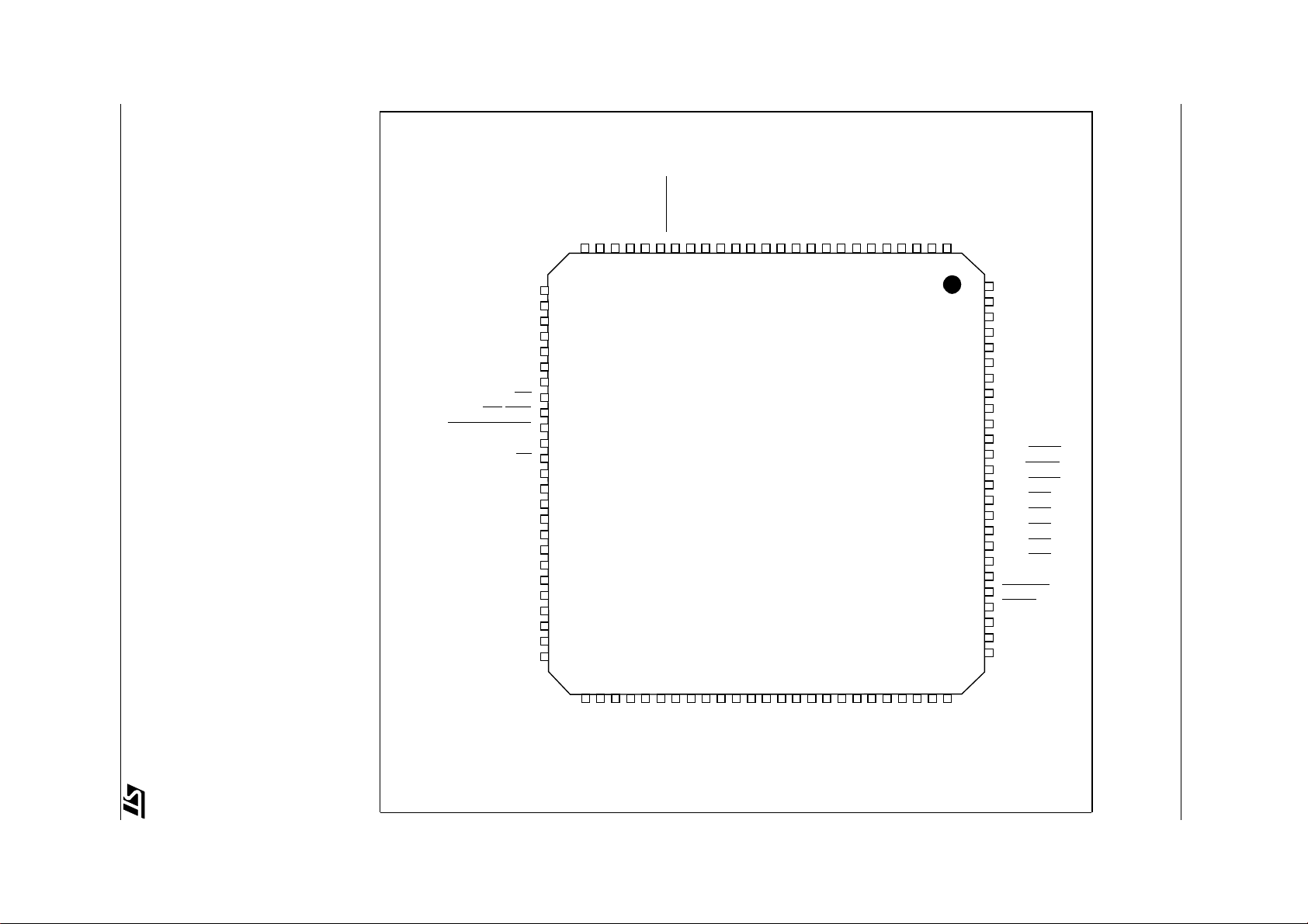
Figure 1 TQFP-100 pin con figuration (top view)
P4.3/A19
V
SS
V
WR/W RL
ALE
V
V
RPD
P0L.0/AD0
P0L.1/AD1
P0L.2/AD2
P0L.3/AD3
P0L.4/AD4
P0L.5/AD5
P0L.6/AD6
P0L.7/AD7
V
V
DD
RD
EA
DD
SS
DD
SS
P4.4/A20/SSPCE1
P4.5/A21/SSPCE0
P4.6/A22/SSPDAT
P4.7/A23/SSPCLK
READY/READY
25
26
2728 293031 323334 3536 373839 404142434445464748 4950
54
53
52
51
P3.10/TxD0
P3.13
18
19
20
21
58
57
56
55
P 3 .6 /T 3 IN
P 3 .7 /T 2 IN
P3.8
P3.9
14
15
16
17
ST10R 172L
62
61
60
59
P3.2/CAPIN
P 3 .5 /T 4 IN
XTAL2
P3.0
V
DD
6
7
8
9
10
11
12
13
70
69
68
67
66
65
64
63
P5.14/T4EUD
P5.15/T2EUD
P 5 .1 3 /T 5IN
XTAL1
V
SS
1
2
3
4
5
100999897969594939291908988878685848382818079787776
P5.12/T6IN
P5.11/T5EUD
P5.10/T6EUD
P7.3/POUT3
P7.2
P7.1
P7.0
P2.11/EX3IN
P2.10/EX2IN
P2.9/EX1IN
P2.8/EX0IN
P6.7/BREQ
P6.6/HLDA
P6.5/HOLD
P6.4/CS4
P6.3/CS3
P6.2/CS2
P6.1/CS1
P6.0/CS0
NMI
RSTOUT
RSTIN
V
DD
V
SS
P1H.7/A15
75
74
73
72
71
1 PIN DESCRIPTION
ST10R172L - PIN DESCR IPTION
P0H.0/AD8
SSVDD
P1H.6/A14
P1H.5/A13
P1H.4/A12
P1H.3/A11
P1H.2/A10
V
P1H.1/A9
P1H.0/A8
P1L.7/A7
P1L.6/A6
P1L.5/A5
P1L.4/A4
P1L.3/A3
P1L.2/A2
P1L.1/A1
P1L.0/A0
P0H.7/AD15
P0H.6/AD14
P0H.5/AD13
P0H.4/AD12
P0H.3/AD11
P0H.2/AD10
P0H.1/AD9
Page 5
ST10R172L - PIN DESCR IPTION
1)
Symbol
P5.10
–P5.15
XTAL1
XTAL2
Pin Number
(TQFP)
98-100
1- 3
Input (I)
Output (O)
Kind
Function
I
I
5S5S6-bit input-only port with Schmitt-Trigger characteristics.
Port 5 pins also serve as timer inputs:
98 I 5S P5.10 T6EUD GPT2 Timer T6 Ext.Up/Down
Ctrl.Input
99 I 5S P5.11 T5EUD GPT2 Timer T5 Ext.Up/Down
Ctrl.Input
100 I 5S P5.12 T6IN GPT2 Timer T6 Count Input
1 I 5S P5.13 T5IN GPT2 Timer T5 Count Input
2 I 5S P5.1 4 T4 EUD GPT1 Timer T4 Ex t. Up / Down
Ctrl.Input
3 I 5S P5.1 5 T2 EUD GPT1 Timer T2 Ex t. Up / Down
Ctrl.Input
5 I 3T X TAL1: Input to the oscillator amplifier and internal clock
generator
6 O 3T XTAL2: Output of the oscillator amplifier circuit.
To clock the device from an external source, drive
XTA L1, while leaving XTAL2 unconnected.
Observe minimum and maximum high/low and
rise/fall times specified in the AC Characteristics.
Table 1 Pin definitions
5/68
1
Page 6
ST10R172L - PIN DESCR IPTION
1)
Symbol
P3.0 –
P3.13
P3.15
Pin Number
(TQFP)
8-21
Input (I)
I/O
Output (O)
Kind
Function
5T 5TA 15-bit (P3.14 is missing) bidirectional I/O port. Port 3 is bit-
wise programmable for input or output via direction bits. For a
22
I/O
pin configured as input, the output driver is put into highimpedance state. Port 3 outputs can be configured as push/
pull or open drain drivers. The following pins have alternate
functions:
9 O 5T P3.1 T6OUT GPT2 Timer T6 toggle latch output
10 I 5T P3. 2 CAPIN GPT2 Register CAPREL capture
input
11 O 5T P3.3 T3OUT GPT1 Timer T3 toggle latch output
12 I 5T P3. 4 T3EUD GPT1 Timer T3 ext.up/down ctrl.input
13 I 5T P3. 5 T4IN GPT1 Timer T4 input for count/gate/
reload/capture
14 I 5T P 3.6 T3IN GPT1 Timer T3 count/ gate input
15 I 5T P3. 7 T2IN GPT1 Timer T2 input for count/gate/
reload/capture
6/68
1
18 O 5T P3.10 TxD0 ASC0 clock/data output (asyn./syn.)
19 I/O 5T P3. 11 RxD0 ASC0 data input (asyn.) or I/O (syn.)
20 O 5T P3.12 BHE
O5T WRH
Ext. Memory High Byte Enable Signal
Ext. Memory High Byte Write Strobe
22 O 5T P3.15 CLKOUT System clock output (=CPU clock)
Table 1 Pin definitions
Page 7
ST10R172L - PIN DESCR IPTION
1)
Symbol
P4.0–
P4.7
Pin Number
(TQFP)
23-26
29-32-
Input (I)
Output (O)
Kind
Function
I/O 5T An 8-bit bidirectional I/O port. Port 8 is bit-wise programmable
for input or output via direction bits. For a pin configured as
input, the output driver is put into high-impedance state.
Port 4 can be used to output the segment address lines for
external bus configuration.
23 O 5T P4.0 A16 Least Significant Segment Addr. Line
... ... ... ... ... ...
26 O 5T P4.3 A19 Segment Address Line
29 O 5T P4.4 A20 Segment Address Line
O 5T SSPCE1 Chip Enable Line 1
30 O 5T P4.5 A21 Segment Address Line
O 5T SSPCE0 SSPChip Enable Line 0
31 O 5T P4.6 A22 Segment Address Line
I/O 5T SSPDAT SSP Data Input/O utpu t Line
RD
WR/
WRL
READY/
READY
32 O 5T P4.7 A23 Most Significant Segment Addr. Line
O 5T SSPCLK SSP Clock Output Line
33 O 5T External Memory Read Strobe. RD is activated for every exter-
nal instruction or data read access.
34 O 5T External Memory Write Strobe. In WR-mode, this pin is acti-
vated for every external data write access. In WRL-mode, this
pin is activated for low byte data write accesses on a 16-bit
bus, and for every data write access on an 8-bit bus.
See WRCFG in the SYSCON register for mode selection.
35 I 5T Ready Input. Active level is programmable. When the Ready
function is enabled, the selected inactive level at this pin dur-
ing an external memory access will f orce t he insertion of mem-
ory cycle time waitstates until the pin returns to the selected
active level. Polarity is pro gram mable.
Table 1 Pin definitions
7/68
1
Page 8
ST10R172L - PIN DESCR IPTION
1)
Symbol
Pin Number
(TQFP)
Input (I)
Output (O)
Kind
Function
ALE 36 O 5T Address Latch Enable Output. Can be used for latching the
address into external memory or an address latch in the multi-
plexed bus modes.
EA
37 I 5T E xt ernal Access Enable pin. Low level at this pin during and
after reset forces the ST10R172L to begin instruction execu-
tion out of external memory. A high level forces execution out
of the internal ROM. The ST10R172L must have this pin tied
to ‘0’.
PORT0:
P0L.0–
P0L.7,
P0H.0 -
P0H.7
41 - 48
51 - 58
I/O 5T PORT0 has two 8-bit bidirectional I/O ports P0L and P0H. It is
bit-wise programmable for input or output via direction bits. For
a pin configured as input, the output driver is put into high-
impedance state.
For exter nal bus configuration, PORT0 acts as address (A)
and address/data (AD) bus in multiplexed bus modes and as
the data (D) bus in demultiplexed bus modes.
Demultiplexed bus modes
Data Path Width: 8-bit 16-bit
P0L.0 – P0L.7: D0 – D7 D0 - D7
P0H.0 – P0H.7: I/O D8 - D15
PORT1:
P1L.0–
P1L.7,
P1H.0 -
P1H.7
8/68
1
59- 66
67, 68
71-76
Multiplexed bus modes
Data Path Width: 8-bit 16-bit
P0L.0 – P0L.7: AD0 – AD7 AD0 - AD7
P0H.0 – P0H.7: A8 – A15 AD8 – AD15
I/O 5T PORT1 has two 8-bit bidirectional I/O ports P1L and P1H. It is
bit-wise programmable for input or output via direction bits. For
a pin configured as input, the output driver is put into high-
impedance state. PORT1 acts as a 16-bit address bus (A) in
demultiplexed bus modes and also after switching from a
demultiplexed bus mode to a multiplexed bus mode.
Table 1 Pin definitions
Page 9
ST10R172L - PIN DESCR IPTION
1)
Symbol
Pin Number
(TQFP)
Input (I)
Output (O)
Kind
Function
RSTIN 79 I 5T Reset Input with Schmitt-Trigger characteristics. Resets the
device when a low level is applied for a specified duration while
the oscillator is running. An internal pullup resi stor enables
power-on reset using only a capacitor connected to
a bonding option, the RSTIN
pin can also be pulled-down for
V
SS
. With
512 internal clock cycles for hardware, software or watchdog
timer triggered resets
RSTOUT
80 O 5T Internal Reset Indication Output. This pin is set to a low level
when the part is executes hardware-, software- or watchdog
timer reset. RSTOUT
remains low until the EINIT (end of ini-
tialization) instruction is executed.
NMI
81 I 5S Non-Maskable Interrupt Input. A high to low transition at this
pin causes the CPU to vector to the NMI trap routine.
P6.0P6.7
If it is not used, NMI
82-89 I/O 5T An 8-bit bidirectional I/O port. Port 6 is bit-wise programmable
for input or output via direction bits. For a pin configured as
should be pulled high externally.
input, the output driver is put into high-impedance state. Port 6
outputs can be configured as push/pull or open drain drivers.
The following Port 6 pins have alternate functions:
82 O 5T P6.0 CS0
Chip Select 0 Output
... ... ... ... ... ...
86 O 5T P6.4 CS4
87 I 5T P 6. 5 HOL D
Chip Select 4 Output
External Master Hold Request Input
(Master mode: O, Slave mode: I)
88 I/O 5T P6.6 HLDA
89 O 5T P6.7 BRE Q
Hold Acknowledge Output
Bus Request Output
Table 1 Pin definitions
9/68
1
Page 10
ST10R172L - PIN DESCR IPTION
1)
Symbol
P2.8 –
P2.11
Pin Number
(TQFP)
Input (I)
Output (O)
Kind
Function
90 - 93 I/O 5T Por t 2 is a 4-bit bidirectional I/O port. It is bit-wise programma-
ble for input or output via di rection bits. For a pin configured as
input, the output driver is put into high-impedance state. Port 2
outputs can be configured as push/pull or open drain drivers.
The following Port 2 pins have alternate functions:
90 I 5T P 2.8 EX0IN Fast External Interrupt 0 Input
... ... ... ... ... ...
93 I 5T P 2.11 EX 3IN Fast Externa l Interrupt 3 Input
P7.0 –
P7.3
94 - 97 I/O 5T Por t 7 is a 4-bit bidirectional I/O port. It is bit-wise programma-
ble for input or output via di rection bits. For a pin configured as
input, the output driver is put into high-impedance state. Port
7outputs can be configured as push/pull or open drain drivers.
The following Port 7 pins have alternate functions:
97 O 5T P7.3 POUT3 PWM (Channel 3) Output
RPD 40 I/O 5T Input timing pin for the return from powerdown circuit and
power-up asynchronous reset.
V
DD
7, 28,
- PO Di gital supply voltage.
38, 49,
69, 78
V
SS
4, 27,
- PO Di gital ground.
39, 50,
70, 77
Table 1 Pin definitions
1) The following I/O kinds are used. Refer to
page 31 for a detailed description.
PO: Power pin
3T: 3 V tolerant pin (voltage max. respect to Vss is -0.5 to VDD + 0.5)
5V: 5 V tolerant pin (voltage max. respect to Vss is -0.5 to 5.5 only if chip is powered)
5S: 5 V tolerant and f ail-safe pin (-0.5-5.5 ma x. voltage w.r.t. Vss ev en if chip is n ot pow-
ered).
10/68
1
ELECTRICAL CHARACTERISTICS
on
Page 11
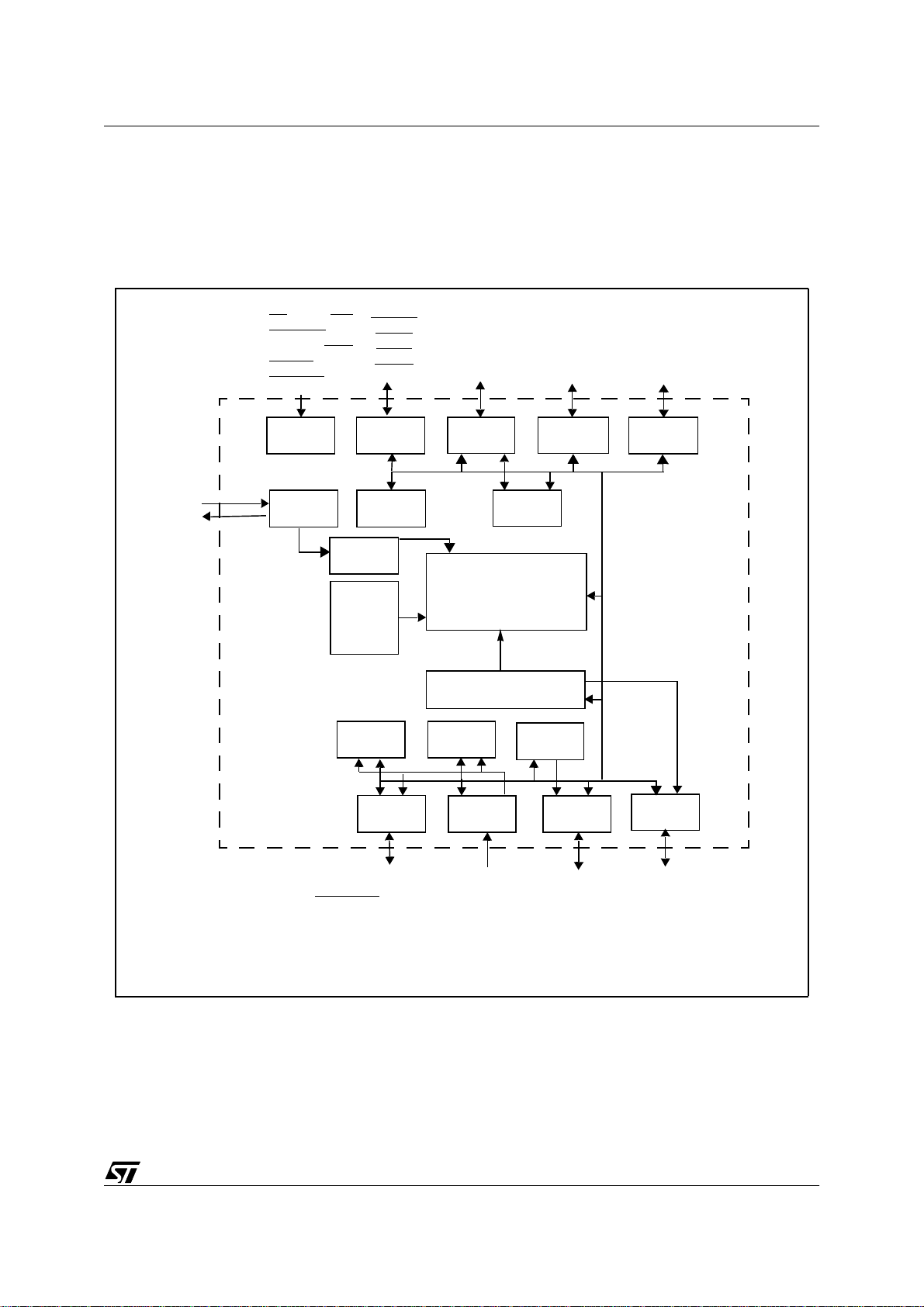
ST10R172L - FUNCTIONAL DESCRIPTION
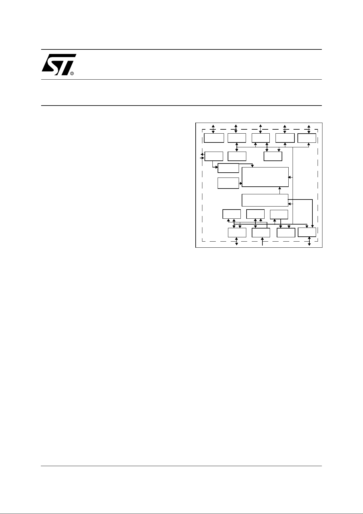
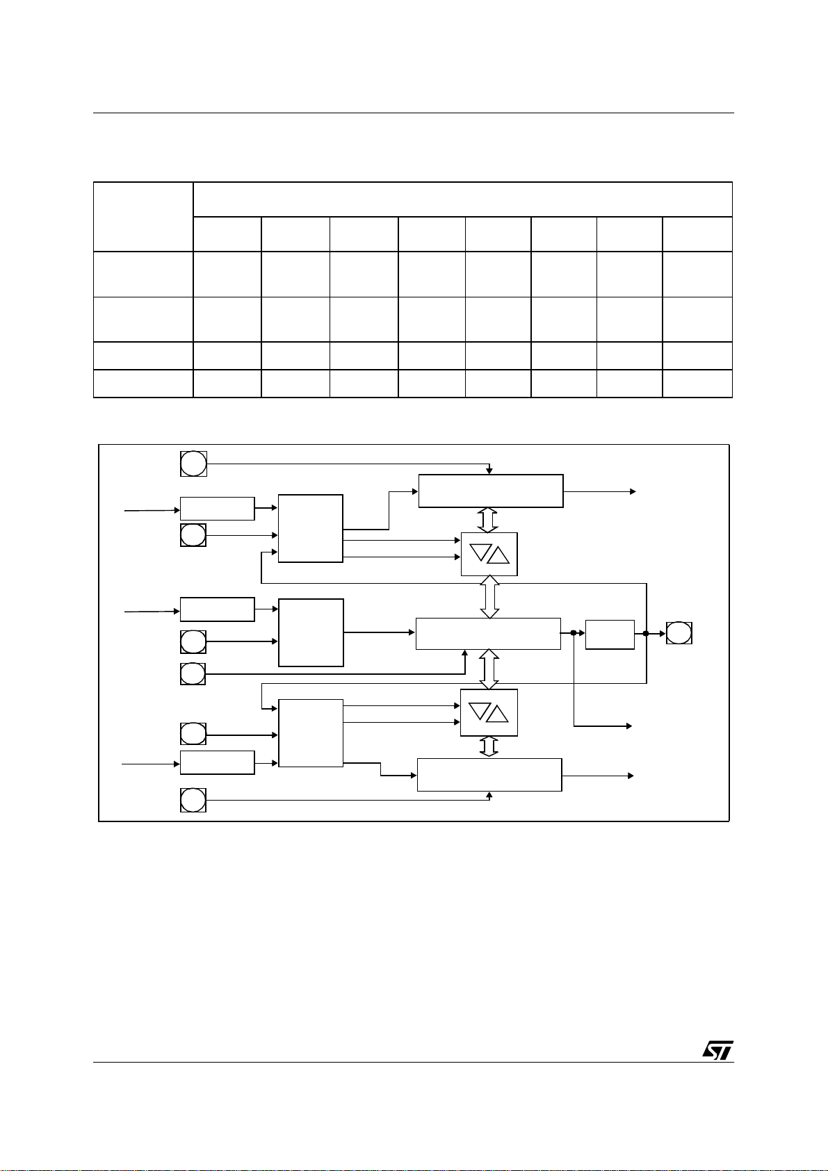
2 FUNCTIONAL DESCRIPTION
ST10R172L architecture combines the advantages of both RISC and CISC processors wi th
an advanced peripheral subsystem. The following block diagram overviews the different onchip components and the internal bus structure.
XTAL1
XTAL2
EA, ALE, RD,
WR/WRL,
READY, NMI,
RSTIN,
RSTOUT
dedicated
pins
OSC
DPRAM
I/O
CS(4:0)
HOLD
HLDA
BREQ
Port 6
8-bit
WDT
PLL
1KByte
ASC GPT1/2
I/O
A(23:16),
SSPCLK,
SSPDAT,
SSPCE(1:0)
A(15:0)
Port 4
8-bit
XSSP
4-bit
ST10 CO RE
Interrupt Controller
&
PEC
PWM
I/O
Port 1
2x8-bit
I/O
I/O, D(7:0)
D(15:8), D(7:0)
A(15:8), AD(7:0)
AD(15:8), AD(7:0)
Port 0
2x8-bit
Port 3
15-bit
I/O
CLKOUT,
BHE/WRH
TxD0, T2IN, T3IN,
T4IN, T3EUD,
T3OUT, CAPIN,
T6OUT
, RxD0,
Figure 2 Block diagram
Port 5
6-bit
I
T2EUD,
T4EUD, T5IN,
T6IN, T5EUD,
T6EUD
Port 7
4-bit
I/O
POUT3
Port 2
4-bit
I/O
EXIN(3:0)
11/68
1
Page 12
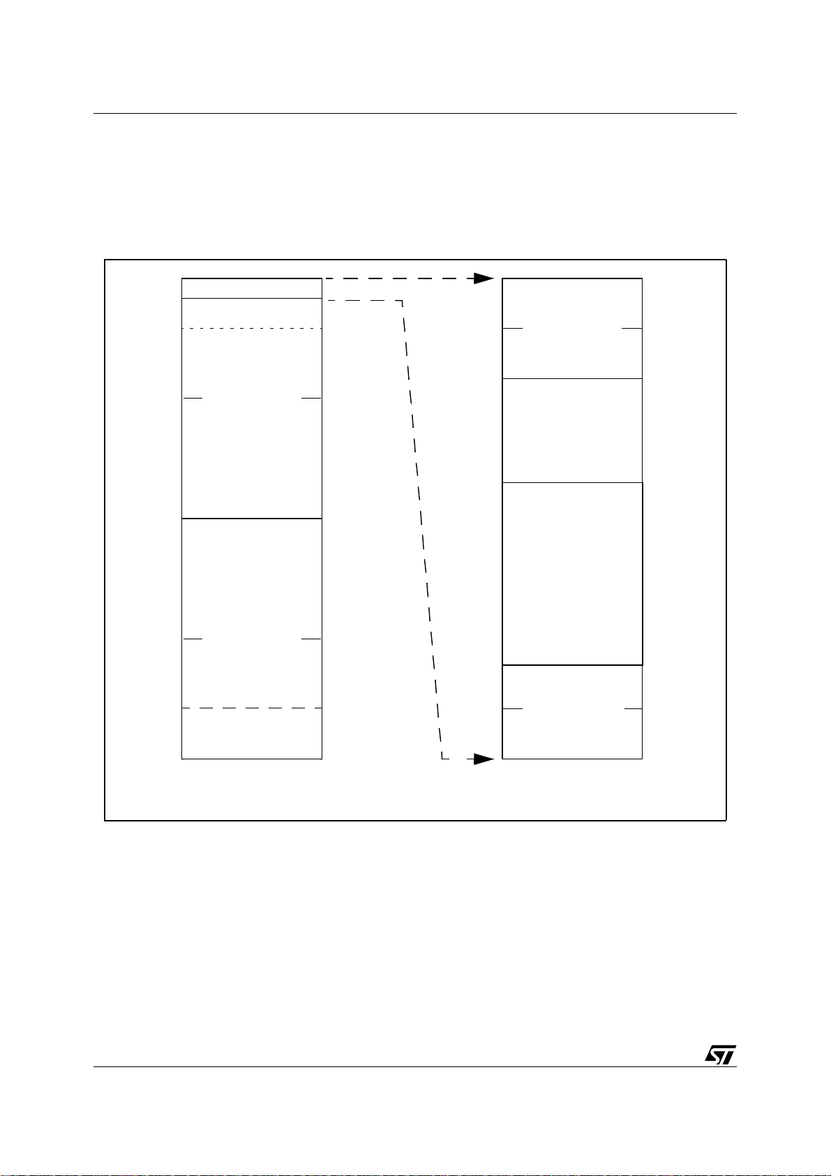
ST10R172L - MEMORY MA PPING
3 MEMORY MAPPING
The ST10R172L is a ROMless device, the internal RAM space is 1 KByte. The RAM address
space is used for variables, register banks, the system stack, the PEC pointers (in 00’FCE0h
- 00’FCFFh) and the bit-addressable space (in 00’FD00h - 00’FDFFh).
00’EFFFh
256 Byte
00’EF00h
00’1FFFh
8K-byte
00’0000h
RAM/SFR
XSSP
External
memory
internal
memory
System Segment 0
64 K-Byte
00’FFFFh
00’F000h
Data Page 3
00’F000h
Data Page 2
00’8000h
Data Page 1
Block 1
00’4000h
Data Page 0
Block 0
00’0000h
00’FF3Fh
00’FF20h
00’FE3Fh
00’FE20h
00’FF3Fh
00’FF20h
00’F03Fh
00’F020h
SFR Area
(reserved)
RAM
ESFR Area
(reserved)
DPRAM / SFR Area
4 K-Byte
00’FFFFh
00’FE00h
1K-Byte
00’FA00h
00’F200h
00’F000h
12/68
1
Figure 3 Memory map
Page 13
ST10R172L - CENTRAL PROCESSING UNIT
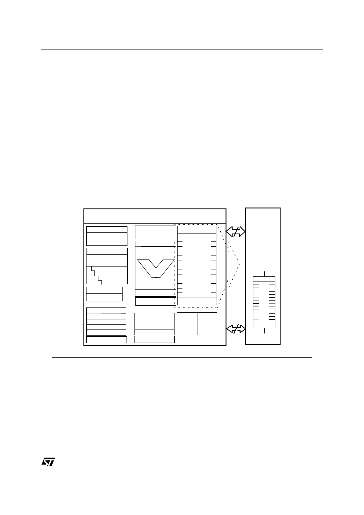
4 CENTRAL PROCESSING UNIT
The main core of the CPU contains a 4-stage instruction pipeline, a separate multiply and
divide unit, a bit-mask generator and a barrel shifter . Most instructions can be ex ecuted in one
machine cycle requiring 40ns at 50MHz CPU clock.
The CPU includes an actual register context consisting of 16 wordwide GPRs physically
located in the on-chip RAM area. A Context Pointer (CP) register determines the base
address of the activ e register bank to be ac cessed b y the CPU . T he number of r egister banks
is only restricted by the available internal RAM space. For easy parameter passing, one
register bank may overlap others.
A system stack of up to 1024 bytes is provided as a storage for temporary data. The system
stack is al located in the on-chip RAM area, and it i s accessed by the C PU via the stac k pointer
(SP) register. Two separate SFR s, STKOV and STKUN, are compared against the stack
pointer value during each stack access to detect stack overflow or underflow.
SP
STKOV
STKUN
Exec. Unit
Instr. Ptr
Instr. Reg
4-Stage
Pipeline
PSW
SYSCON
BUSCON 0
BUSCON 1
BUSCON 2
BUSCON 3
BUSCON 4
Data Pg. Ptrs
CPU
MDH
MDL
Mul./Div.-HW
Bit-Mask Gen.
ALU
16-Bit
Barrel-Shift
Context Ptr
ADDRSEL 1
ADDRSEL 2
ADDRSEL 3
ADDRSEL 4
Code Seg. Ptr.
R15
General
Purpose
Registers
R0
IDX0
QR0
IDX1
QX1QX0
QR1
Figure 4 CPU block diagram
16
16
Internal
RAM
1KByte
R15
R0
13/68
1
Page 14

ST10R172L - INTERRUPT AND TRAP FUNCTIONS
5 INTERRUPT AND TRAP FUNCTI ONS
The architecture of the ST10R172L supports s everal mechanisms for fast and flexible
response to the service requests that can be generated from various sources, internal or
external to the microcontroller. Any of these interrupt requests can be programmed to be
serviced, either by the Interrupt Controller or by the Peripheral Event Controller (PEC).
In a standard interrupt service, program executi on is suspended and a branch to the interrupt
service routine is performed. For a PEC service, just one cycle is ‘stolen’ from the current
CPU activity. A PEC service is a single, byte or word data transfer between any two memory
locations, with an additional increment of either the PEC source or the destination pointer. An
individual PEC transfer counter is decremented for each PEC servic e, except in the
continuous transfer mode. When this counter reaches zero , a standard interrupt is performed
to the corresponding source-related vector location. PEC services are very well suited, for
example, to the transmission or reception of blocks of data. The ST10R172L has 8 PEC
channels, each of which offers fast interrupt-driven data transfer capabilities.
A separate control register which contains an interrupt request flag, an interrupt enable flag
and an interrupt priority bitfield, exists f or each of the possib le interrupt sources. Via it s related
register, each source can be programmed to one of sixteen interrupt priority levels. Once
having been accepted by the CPU, an interrupt service can only be interrupted by a higher
priority service request. For standard interrupt processing, each of the possible interrupt
sources has a dedicated vector location.
Fast external interrupt inputs are provided to service external interrupts with high precision
requirements. These fast interrupt inputs, feature programmable edge detection (rising edge,
falling edge or both edges).
Software interrupts are supported by means of the ‘TRAP’ instruc tion in combination with an
individual trap (interrupt) number.
14/68
1
Page 15
5.1 Interrupt Sources
ST10R172L - INTERRUPT AND TRAP FUNCTIONS
Source of Interru pt or PEC
Service Request
External Interrupt 0 CC8IR CC8IE CC8INT 60h 18h
External Interrupt 1 CC9IR CC9IE CC9INT 64h 19h
External Interrupt 2 CC10IR CC10IE CC10INT 68h 1Ah
External Interrupt 3 CC11IR CC11IE CC11INT 6Ch 1Bh
GPT1 Timer 2 T2IR T2IE T2INT 88h 22h
GPT1 Timer 3 T3IR T3IE T3INT 8Ch 23h
GPT1 Timer 4 T4IR T4IE T4INT 90h 24h
GPT2 Timer 5 T5IR T5IE T5INT 94h 25h
GPT2 Timer 6 T6IR T6IE T6INT 98h 26h
GPT2 CAPREL Register CRIR CRIE CRINT 9Ch 27h
ASC0 T ransmit S0TIR S0TIE S0TINT A8h 2Ah
ASC0 Transmit Buffer S0TBIR S0TBIE S0TBINT 11Ch 47h
Request
Flag
Enable
Flag
Interrupt
Vector
Vector
Location
Trap
Number
ASC0 Receive S0RIR S0RIE S0RINT ACh 2Bh
ASC0 Error S0EIR S0EIE S0EINT B0h 2Ch
PWM Channel 3 PWMIR PWMIE PWMINT FCh 3Fh
SSP Interrupt XP1IR X P 1IE X P1I NT 104h 41h
PLL Unlock XP3I R XP3IE X P3I NT 10Ch 43h
Table 2 List of possible interrupt sources, flags, vector and trap numbers
15/68
1
Page 16
ST10R172L - INTERRUPT AND TRAP FUNCTIONS
5.2 Hard w are traps
Exceptions or error conditions that arise during run-time are called Hardware T raps. Hardware
traps cause immediate non-maskable system reaction similar to a standard interrupt service
(branching to a dedicated vector table location). The occurrence of a hardware trap is
additionally signified by an individual bit in the trap flag register (TFR). Except when another
higher prioritized trap service is in progress, a hardware trap will interrupt any actual progr am
ex ecution. In turn, hardware trap services can not normally be interrupted by standard or PEC
interrupts. The following tab le shows all of the possible ex ceptions or error conditions that can
arise during run-time:
Exception Condition T rap Flag Trap Vector
Vector
Location
Reset Functions:
Hardware Reset RESET 00’0000
Software Reset RESET 00’0000
Watchdog Timer Overflow RESET 00’0000
Class A Hardware Traps:
Non-Maskable Interrupt NMI NMITRAP 00’ 0008
Stack Overflow STKOF STOTRAP 00’0010
Stack Underflow STKUF STUTRAP 00’0018
Class B Hardware Traps:
Undefined opcode UNDOPC BTRAP 00’0028h 0A
Protected instruction fault PRTFLT BTRAP 00’0028h 0A
Illegal word operand access ILLOPA BTRAP 00’0028h 0A
Illegal instruction access ILLINA BTRAP 00’0028h 0A
Trap
Number
h 00h III
h 00h III
h 00h III
h 02h II
h 04h II
h 06h II
h I
h I
h I
h I
Trap
Priority
Illegal external bus access ILLBUS BTRAP 00’0028h 0A
Reserved [2C
h – 3Ch][0Bh – 0Fh]
Software Traps
TRAP Instruction Any [00’0000
– 00’01FC
steps of 4
Table 3 Exceptions or error conditions
16/68
1
h I
h
Any
[00
h]
h
h – 7Fh]
Current
CPU
Priority
Page 17

ST10R172L - PARALLEL PORTS
6 PARALLEL PORTS
The ST10R172L provides up to 77 I/O lines organized into 7 input/output ports and one input
port. All port lines are bit-addressable, and all input/output lines are individually (bit-wise)
programmable as inputs or outputs by direction registers. The I/O ports are true bi directional
ports which are switched to high impedance state when configured as inputs. The output
drivers of three I/O ports can be configured (pin by pin) for push/pull operation or open-drain
operation by control registers. During the internal reset, all port pins are configured as inputs.
All port lines have programmable alternate input or output functions associated with them.
PORT0 and PORT1 may be used as address and data lines when accessing external
memory , while P ort 4 outputs the additional segment address bits A23/19/17...A16 in systems
where segmentation is enabled to access more than 64 KBytes of memory. Port 6 provides
optional bus arbitration signals (BREQ
alternate functions of timers, serial interfaces, the optional bus control signal BHE
system clock output (CLKOUT). Port 5 is used for timer control signals. Port 2 lines can be
used as fast external interrupt lines. Port 7 includes alternate function for the PWM signal. All
port lines that are not used for these alternate functions may be used as general purpose I/O
lines.
, HLDA, HOLD) and chip select signals. Port 3 includes
and the
7 EXTE RNAL BUS CONTROLLER
All external memory accesses are performed by the on-chip External B us Controller which
can be programmed either to single chip mode when no external memory is required, or to the
following external memor y ac ces s modes:
16-bit data, demultiplexed 16-/18-/20-/24-bit addresses
16-bit data, multiplexed 16-/18-/20-/24-bit addresses
8-bit data, multiplexed 16-/18-/20-/24-bit addresses
8-bit data, demultiplexed 16-/18-/20-/24-bit addresses
In the demultiplex ed b us modes, addresses are output on PORT1 and data is input/output on
PORT0/P0L, respectively. In the multiplex ed bus modes both addresses and data use PORT0
for input/output.
Memory cycle time, memory tri-state time, length of ALE and read write delay are
programmable so that a wide range of different memory types and external peripherals can be
used. Up to 4 independent address windows can be defined (via ADDRSELx / BUSCONx
register pairs) to access different resources with different bus characteristics. These address
windows are arranged hier archically where BUSCON4 ov errides BUSCON3 etc. All accesses
to locations not covered by these 4 address windows are controlled by BUSCON0. Up to 5
exte r nal CS
Access to very slow memories is supported by the READY function.
signals (4 windows plus default) can be generated to reduce external glue logic.
A HOLD
/HLDA protocol is available for bus arbitration so that external resources can be
shared with other bu s masters. In slav e mode, the s lave controller can be connec ted to another master controller without glue logic. For applications which require less than 16 MBytes
17/68
1
Page 18
ST10R172L - PWM MODULE
of external memory space, the address space can be restricted to 1 MByte, 256 KByte or to 64
KByte.
8PWM MODULE
A 1-channel Pulse Width Modulation (PWM) Module operates on channel 3. The pulse width
modulation module can generate up to four PWM output signals using edge-aligned or centrealigned PWM. In addition, the PWM module can generate PWM burst signals and single shot
outputs. The table below shows the PWM frequencies for different resolutions. The level of
the output signals is selectable and the PWM module can generate interrupt requests.
Mode 0
edge aligned
CPU clock/1 20ns 195.3 KHz 48.83KHz 12.21KHz 3.052KHz 762.9Hz
CPU clock/64 1.28ns 3.052KHz 762.9Hz 190.7Hz 47.68Hz 11.92Hz
Mode 1
center aligned
CPU clock/1 20ns 97.66KHz 24.41KHz 6.104KHz 1.525KHz 381.5Hz
CPU clock/64 1.28ns 1.525Hz 381.5 Hz 95.37Hz 23.84Hz 0Hz
Resolution 8-bit 10-bit 12-bit 14-bit 16-bit
Resolution 8-bit 10-bit 12-bit 14-bit 16-bit
Table 4 PWM unit frequencies and resolution at 50MHz CPU clock
18/68
1
Page 19

ST10R172L - GENERAL PURPOSE TIMERS
9 GEN ERAL PURPOSE TIM ERS
The GPTs are flexible multifunctional timer/counters used f or time-related tasks such as e vent
timing and counting, pulse width and duty cycle measurements, pulse generation or pulse
multiplication. The GPT unit contains five 16-bit timers, organized in two separate modules,
GPT1 and GPT2. Each timer in each module m ay operate independently in a number of
different modes, or may be concatenated with another timer of the same module.
9.1 GPT1
Each of the three timers T2, T3, T4 of the GPT1 module can be configured individually f or one
of four basic modes of operation: timer, gated timer, counter mode and incremental
interface mode. In timer mode, the input clock for a timer is derived from the CPU clock,
divided by a programmable prescaler. In counter mode, the timer is clocked in reference to
external events. Pulse width or duty cycle measurement is supported in gated timer mode
where the operation of a timer is controlled by the ‘gate’ level on an external input pin. For
these purposes, each timer has one associated port pin (TxIN) which serves as gate or clock
input. Table 5 GPT1 timer input frequencies, resolution and periods lists the timer input
frequencies, resoluti on and periods f or eac h pre-s caler option at 50MHz CPU cl oc k. T his al so
applies to the Gated Timer Mode of T3 and to the auxiliary timers T2 and T4 in Timer and
Gated Timer Mode
The count direction (up/down) for each timer is programmable by software or may additionally
be altered dynamically by an external signal on a port pin (TxEUD).
In Incremental Interface Mode, the GPT1 timers (T2, T3, T4) can be directly connected to the
incremental position sensor signals A and B by their respective inputs TxIN and TxEUD.
Direction and count signals are internally derived from these two input signals so that the
contents of the respective timer Tx corresponds to the sensor position. The third position
sensor signal TOP0 can be connected to an interrupt input.
Timer T3 has output toggle latches (TxOTL) which changes state on each timer over-flow/
underflow. The state of this latch may be output on port pins (TxOUT) e. g. for time out
monitoring of external hardware components, or ma y be used internally to clock timers T2 and
T4 for measuring long time periods with high resolution.
In addition to their basic operating modes, timers T2 and T4 may be configured as reload or
capture registers f or timer T3. When used as capture or reload registers, timers T2 and T4 are
stopped. The contents of timer T3 is captured into T2 or T4 in response to a signal at their
associated input pins (TxIN). Timer T3 is reloaded with the contents of T2 or T4 triggered
either by an ex ternal signal or by a selectabl e state transiti on of its toggle latch T3O TL. When
both T2 and T4 are configured to alternately reload T3 on opposite state tr ansitions of T 3O T L
with the low and high times of a PWM signal, this signal can be constantly generated without
software intervention.
19/68
1
Page 20
ST10R172L - GENERAL PURPOSE TIMERS
Timer input selection
F
=50MHz
CPU
000b 001b 010b 011b 100b 101b 110b 111b
Prescaler
8 16 32 64 128 256 512 1024
Factor
Input
Frequency
6.25 MHz 3.125
MHz
1.5625
MHz
781
KHz
391
KHz
195
KHz
97.5
KHz
48.83
KHz
Resolution 160ns 320ns 640ns 1.28 us 2. 56 us 5.12 us 10.24 us 20.48 us
Period 10.49ms 20 .97 ms 41 .94 ms 83 .88ms 168ms 336m s 672ms 1. 342s
Table 5 GPT1 timer input frequencies, resolution and periods
T2EUD
CPU Clock
T2IN
CPU Clock
T3EUD
T3IN
T4IN
CPU Clock
T4EUD
2n n= 3 ...10
n
n= 3 ...10
2
n
n= 3 ...10
2
T2
Mode
T3
Mode
T4
Mode
GPT1 Timer T2
Reload
Capture
GPT1 Timer T3
U/D
Capture
Reload
GPT1 Timer T4
U/D
Interrupt
Request
T3OUT
T3OTL
Interrupt
Request
Interrupt
Request
U/D
20/68
1
Figure 5 GPT1 block diagram
Page 21
ST10R172L - GENERAL PURPOSE TIMERS
9.2 GPT2
The GPT2 module provides precise event control and time measurement. It includes two
timers (T5, T6) and a capture/reload register (CAPREL). Both timers can be clocked with an
input clock derived from the CPU clock via a programmable prescaler or with e xternal signals.
The count direction (up/down) for each timer is programmable by software or altered
dynamically by an exter nal signal on a port pin (TxEUD). Concatenation of the timers is
supported by the output toggle latch (T6OTL) of timer T6, which changes its state on each
timer overflow/underflow.
The state of T6OT L may be used to cloc k timer T5, or ma y be output on a port pin T6OUT. The
overflow s/underflows of timer T6 reload the CAPREL register. The CAPREL register captures
the contents of T5 based on an external signal transition on the corresponding port pin
(CAPIN), and timer T5 may optionally be cleared after the capture procedure. This allows
absolute time differences to be measured or pulse multiplication to be performedwithout
software overhead.
Timer input selection
F
=50MHz
CPU
000b 001b 010b 011b 100b 101b 110b 111b
Prescaler
Factor
Input
Frequency
Resolution 80ns 160 ns 320ns 640ns 1.28 us 2.56 us 5.12 us 10.24 us
Period 5.24ms 10.49ms 20.97ms 41.94ms 8 3.88 ms 167.7ms 335.5m s 671m s
4 8 16 32 64 128 256 512
12.5 MHz 6.25 MHz 3.125
MHz
1.563
MHz
781
KHz
391
KHz
195
KHz
97.6
KHz
Table 6 GPT2 timer input frequencies, resolution and periods
21/68
1
Page 22

ST10R172L - SERIAL CHANNELS
T5EU D
CPU Clock
T5IN
CAPIN
T6IN
CPU Clock
T6EUD
2n n=2...9
n
n=2...9
2
U/D
T5
GP T2 Timer T5
Mode
Clear
Capture
GPT2 CAPREL
T6
Mode
GPT2 Timer T6
U/D
Figure 6 GPT2 block diagram
Reload
Toggle FF
T60TL
Inte rr upt
Request
Interrupt
Request
Inte rr upt
Request
T6OUT
10 SERIAL CHANNELS
Serial communication with other microcontrollers, proces sors, terminals or external peripheral
components is provided by two serial interfaces with different functionality, an Asynchronous/
Synchronous Serial Channel (ASC0) and a Synchronous Serial Port (SSP).
ASC0
A dedicated baud rate generator sets up standard baud rates without oscillator tuning. 3
separate interrupt vectors are provided for transmission, reception, and erroneous reception.
In asynchronous mode, 8- or 9-bit data frames are transmitted or received, preceded by a start
bit and terminated by one or two stop bits. Fo r multiprocessor comm unication, a mechanism
to distinguish address from data bytes has been included (8-bit data + wake up bit mode).
In synchronous mode, the ASC0 transm its or receives bytes (8 bits) synchronously to a s hift
clock which is generated by the ASC0. The ASC0 always shifts the LSB first. A loop back
option is available for testing purposes.
A number of optional hardware error detection capabilities have been included to increase the
reliability of data transfers. A parity bit can be generated automatically on transmission, or
checked on reception. Framing error detection recognizes data frames with missing stop bits.
An overrun error is generated if the last character received was not read out of the receive
buffer register at the time the reception of a new character is complete.The table below lists
22/68
1
Page 23

ST10R172L - SERIAL CHANN ELS
various commonly used baud rates together with the required reload values and the deviation
errors compared to the intended baudrate.
S0BRS = ‘0’, f
Baud Rate
(Baud)
1562500 0.0% / 0.0% 0 000
= 50MHz S0BRS = ‘1’, f
CPU
Deviation Error Reload Value
/ 0000
H
Baud Rate
(Baud)
1041666 0.0% / 0.0% 0000H / 0000
H
= 50MHz
CPU
Deviation Error Reload Value
56000 +3.3% / -0.4% 001AH / 001BH56000 +3.3% / -2.1% 0011H / 0012
38400 +1.7% / -0.8% 0027H / 0028
19200 +0.5% / -0.8% 0050H / 0051
9600 +0.5% / -0.1% 00A1H/ 00A2
4800 +0.2% / -0.1% 0144H / 0145
38400 +0.5% / -3.1% 001AH / 001B
H
19200 +0.5% /-1.4% 0035H / 0036
H
9600 +0.5% / -0.5% 006BH / 006C
H
4800 0.0% / -0.5% 00D8H / 00D9
H
2400 0.0% / -0.1% 028AH / 028BH2400 0.0% / -0.2% 01B1H / 01B2
1200 0.0% / -0.1% 0515H / 0516
1200 0.0% / -0.1% 0363H / 0364
H
600 0.0% / 0.0% 0A2BH / 0A2CH600 0.0% / -0.1% 06C7H / 06C8
190 +0.4% /+0.4% 1FFFH / 1FFFH75 0.0% / 0.0% 363FH / 3640
127 +0.1% / +0.1% 1FFFH / 1FFF
H
H
H
H
H
H
H
H
H
H
H
Table 7 Commonly used baud rates, required reload values and deviation errors
SSP transmits 1...3 bytes or receives 1 byte after sending 1...3 bytes synchronously to a shift
clock which is generated b y the SSP. T he SSP can s tart shifting with the LSB or with the MSB
and is used to select shifting and latching clock edges, and clock polarity . Up to two chip select
lines may be activ ated in order to direct data transf ers to one or both of two peripheral devices.
When the SSP is enabled, the four upper pins of Port4 can not be used as general purpose
IO. Note that the segment address selection done via the system st art-up configuration during
reset has priority and overrides the SSP functions on these pins.
SSPCKS Value Synchronous baud rate
000 SSP clock = CPU clock divided by 2 25 MBit/s
001 SSP clock = CPU clock divided by 4 12.5 MBit/s
010 SSP clock = CPU clock divided by 8 6.25 MBit/s
Table 8 Synchronous baud rate and SSPCKS reload values
23/68
1
Page 24

ST10R172L - WATCHDOG TIMER
SSPCKS Value Synchronous baud rate
011 SSP clock = CPU clock divided by 16 3.13 MBit/s
100 SSP clock = CPU clock divided by 32 1.56 MBit/s
101 SSP clock = CPU clock divided by 64 781 KBit/s
110 SSP clock = CPU clock divided by 128 391 KBit/s
111 SSP clock = CPU clock divided by 256 195 KBit/s
Table 8 Synchronous baud rate and SSPCKS reload values
11 WATCHDOG TIMER
The Watchdog Timer is a fail-safe mechanism which limits the malfunction time of the
controller . The Watchdog Timer is always enabled after device reset and can only be disabled
in the time interval until the EINIT (end of initialization) instruction has been executed. In this
way, the chip’s start-up procedure is always monitored. The software must be designed to
service the Watchdog Timer before it overflows. If, due to hardware or software related
failures, the software fails to maintain the Watchdog Timer, it will overflow generating an
internal hardware reset and pulling the RSTOUT
components.
pin low to reset external hardware
The Watchdog Timer is a 16-bit timer, clocked with the system clock divided either by 2 or by
128. The high byte of the Watchdog Timer register can be set to a pre-specified reload value
(stored in WDTREL) in order to allow further variation of the monitored time interval. Each
time it is serviced by the application software, the high byte of the Watchdog Timer is
reloaded. The table below shows the watchdog time range which for a 50MHz CPU clock
rounded to 3 significant figures.
Reload value
in WDTREL
FF
H
00
H
Prescaler for f
2 (WD TIN = ‘0’ ) 128 (WDTIN = ‘ 1 ’)
10.24 µs 655 µs
2.62 ms 168 ms
CPU
Table 9 Watchdog timer range
24/68
1
Page 25

ST10R172L - SYSTEM R ESET
12 SYSTEM RESET
The following type of reset are implemented on the ST10R172L:
Asynchronous hardware reset: Asynchronous reset does not require a stabilized clock
signal on XTAL1 as it is not internally resynchronized, it resets the microcontroller into its
default reset state. Asynchronous reset is required on chip power-up and can be used during
catastrophic situations. The rising edge of the RSTIN pin is internally resynchronized before
exiting the reset condition, therefore, only the entry to hardware reset is asynchronous.
Synchronous hardware reset (warm reset): A war m synchronous hardware reset is
triggered when the reset input signal RSTIN
immediately (asynchronously) set in high impedance, RSTOUT
negation is detected, a short transition period elapses, during which pending internal hold
states are cancelled and any current internal access cycles are completed, external bus
cycles are aborted. Then, the internal reset sequence is active for 1024 TCL (512 CPU clock
cycles). During this reset sequence, if bit BDRSTEN was previously set by software (bit 5 in
SYSCON register), RSTIN
pin is driven low and internal reset signal is asserted to reset the
microcontroller in its default state . Note that after all reset sequence, bit BDRSTEN is cleared.
After the reset sequence has been completed, the RSTIN input is sampled. When the reset
input signal is active at that time the internal reset condition is prolonged until RSTIN
becomes inactive.
is latched low and Vpp pin is high. The I/Os are
is driven low. After RSTIN
Software reset: The reset sequence can be trigger ed at any time by the protected
instruction SRST (software reset). This instruction can be executed deliberately within a
program, e.g. to leave bootstrap loader mode, or on a hardware trap that reveals a system
failure. As for a synchronous hardware reset, the reset sequence lasts 1024 TCL (512 CPU
clock cycles), and drives the RSTIN
pin low.
Watchdog timer reset: When the watchdog timer is not disabled during the initialization or
serviced regularly during program execution it will overflow and trigger the reset sequence.
Unlike hardware and software resets, the watchdog reset completes a running external bus
cycle if this bus cycle does not use READY
programmed waitstates. When READY
, or if READY is sampled active (low) after the
is sampled inactive (high) after the programmed
waitstates the running external bus cycle is aborted. Then the internal reset sequence is
started. The watchdog reset cannot occur while the ST10R 172L is in bootstrap loader mode.
Bidirectional reset: This reset makes the watchdog timer reset and software reset
externally visible. It is active for the duration of an internal reset sequences caused by a
watchdog timer reset and software reset. Therefore, the bidirectional reset transforms an
internal watchdog timer reset or software reset into an external hardware reset with a
minimum duration of 1024 TCL.
13 POWER REDUCTION MODES
Two different power reduction modes with different levels of power reduction can be entered
under software control.
25/68
1
Page 26

ST10R172L - SPECIAL FUNCTION REGISTERS
In Idle mode the CPU is stopped, while the peripherals continue their operation. Idle mode
can be terminated by any reset or interrupt request.
In Po wer Do wn mod e both the CPU and the peripheral s are stopped. P o wer Down mode can
now be configured by software in order to be terminated only by a hardware reset or by an
external interrupt source on fast external interrupt pins.
All external bus actions are completed before Idle or Power Down mode is entered. However,
Idle or Power Down mode is not entered if READY is enabled, but has not been activated
(driven low f or negativ e polarity, or driven high for positiv e pol arity) during the last bus access.
14 SPECIAL FUNCTION REGISTERS
The following table lists all ST10R172L SFRs in alphabetical order.
Bit-addressable SFRs are marked with the letter “b” in column “Name”. SFRs within the
Extended SFR-Space (ESFRs) are marked with the letter “E” in column “Physical Address”.
An SFR can be specified by its individual mnemonic name. Depending on the selected
addressing mode, an SFR can be accessed by its physical address (using the Data Page
Pointers), or by its short 8-bit address (without using the Data Page Pointers).
Name
ADDRSEL1 FE18h 0Ch Address Select Register 1 0000h
ADDRSEL2 FE1Ah 0Dh Address Select Register 2 0000h
ADDRSEL3 FE1Ch 0E h Address Select Register 3 0000h
ADDRSEL4 FE1Eh 0Fh Address Select Register 4 0000h
BUSCON0 b FF0Ch 86h Bus Configuration Register 0 0XX0h
BUSCON1 b FF14h 8Ah Bus Configuration Register 1 0000h
BUSCON2 b FF16h 8Bh Bus Configuration Register 2 0000h
BUSCON3 b FF18h 8Ch Bus Configuration Register 3 0000h
BUSCON4 b FF1Ah 8Dh Bus Configuration Register 4 0000h
CAPREL FE4A h 25h GPT2 Capture/Reload Register 0000h
CC8IC b FF88h C4h EX0IN Interrupt Control Register 0000h
CC9IC b FF8Ah C5h EX1IN Interrup t Control Register 00 00h
Physical
Address
8-Bit
Address
Description
Reset
Value
CC10IC b FF8Ch C6h EX2IN Interrupt Control Register 00 00h
Table 10 Special functional registers
26/68
1
Page 27

ST10R172L - SPECIAL FUNCTION REGISTERS
Name
CC11IC b FF8E h C7h EX3IN Interrupt Control Register 0000h
CP FE10h 08h CPU Context Pointer Register FC00h
CRIC b FF6Ah B5h GPT2 CAPREL Interrupt Control Register 0000h
CSP FE08h 04h CPU Code Segment Pointer Register (read only) 0000h
DP0L b F100h E 80h P0L Direction Control Register 00h
DP0H b F102h E 81h P0h Direction Control Register 00h
DP1L b F104h E 82h P1L Direction Control Register 00h
DP1H b F106h E 83h P1h Direction Control Register 00h
DP2 b FFC2h E1h Port 2 Direction Control Register -0--h
DP3 b FFC6h E3h Port 3 Direction Control Register 0000h
DP4 b FFCAh E5h Port 4 Direction Control Register 00h
DP6 b FFCEh E7h Port 6 Direction Control Register 00h
Physical
Address
8-Bit
Address
Description
Reset
Value
DP7 b FFD2h E9h Port 7 Direction Control Register -0h
DPP0 FE00h 00h CPU Data Page Po inter 0 Register (10 bits) 00 00h
DPP1 FE02h 01h CPU Data Page Po inter 1 Register (10 bits) 00 01h
DPP2 FE04h 02h CPU Data Page Po inter 2 Register (10 bits) 00 02h
DPP3 FE06h 03h CPU Data Page Po inter 3 Register (10 bits) 00 03h
EBUSCON b F10Eh E 87H Extended BUSC O N register 0000h
EXICON b F1C0h E E0h External Interrupt Control Register 0000h
IDCHIP F07Ch E 3Eh Device Identifier Register 1101h
IDMANUF F07Eh E 3Fh Manufacturer/Process Identifier Register 0201h
IDMEM F07Ah E 3Dh On-chip Memory Identifier Register 0000h
IDPROG F078h E 3Ch Programming Voltage Identifier Register 0000h
MDC b FF0Eh 87h CPU Multiply Divide Control Register 0000h
MDH FE0Ch 06h CPU Multiply Divide Register – High Word 0000h
MDL FE0Eh 07h CPU Multiply Divide Register – Low Word 0000h
Table 10 Special functional registers
27/68
1
Page 28

ST10R172L - SPECIAL FUNCTION REGISTERS
Name
ODP2 b F1C2h E E1h Port 2 Open Drain Control Register -0--h
ODP3 b F1C6h E E3h Port 3 Open Drain Control Register 0000h
ODP6 b F1CEh E E7h Port 6 Open Drain Control Register 00h
ODP7 b F1D2h E E9h Port 7 Open Drain Control Register -0h
ONES FF1Eh 8Fh Constan t Value 1’s Register (read only) FFFFh
P0L b FF00h 80h Port 0 Low Register (Lower half of PORT0) 00h
P0H b FF02h 81 h Port 0 High Register (Upper half of PORT0) 00h
P1L b FF04h 82h Port 1 Low Register (Lower half of PORT1) 00h
P1H b FF06h 83 h Port 1 High Register (Upper half of PORT1) 00h
P2 b FFC0h E0h Port 2 Register (4 bits) -0--h
P3 b FFC4h E2h Port 3 Register 0000h
P4 b FFC8h E4h Port 4 Register (8 bits) 00h
Physical
Address
8-Bit
Address
Description
Reset
Value
P5 b FFA2h D1h Port 5 Register (read only) XXXXh
P6 b FFCCh E6h Port 6 Register (8 bits) 00h
P7 b FFD0h E8h Port 7Register (4 bits) -0h
PECC0 FEC0h 60h PEC Channel 0 Control Register 0000h
PECC1 FEC2h 61h PEC Channel 1 Control Register 0000h
PECC2 FEC4h 62h PEC Channel 2 Control Register 0000h
PECC3 FEC6h 63h PEC Channel 3 Control Register 0000h
PECC4 FEC8h 64h PEC Channel 4 Control Register 0000h
PECC5 FECAh 65h PEC Channel 5 Control Register 0000h
PECC6 FECCh 66h PEC Channel 6 Control Register 0000h
PECC7 FECEh 67h PEC Channel 7 Control Register 0000h
PP3 F03Eh E 1Fh PWM Module Period Register 3 0000h
PSW b FF10h 88h CPU Program Status Word 0000h
PW3 FE36h 1Bh PW M Module Pulse Widt h Register 3 0000h
28/68
1
Table 10 Special functional registers
Page 29

ST10R172L - SPECIAL FUNCTION REGISTERS
Name
Physical
Address
8-Bit
Address
Description
Reset
Value
PWMCON0 b FF30h 98h PWM Module Control Register 0 00 00h
PWMCON1 b FF32h 99h PWM Module Control Register 1 00 00h
PWMIC b F17Eh E BFh PW M Module Interr upt Control Register 00 00h
RP0H b F108 h E 84h System Start-up Configuration Register (Rd. only) XXh
S0BG FEB4h 5Ah Serial Channel 0 baud rate generator reload reg 0000h
S0CON b FFB0h D8h Ser ial Channel 0 Control Register 0000h
S0EIC b FF70 h B8 h Serial Channel 0 Error Interrupt Control Register 0000h
S0RBUF FEB2h 59h S erial Channel 0 receive buffer reg. (rd only) XXh
S0RIC b FF6Eh B7h Serial Channel 0 Receive Interrupt Control Reg. 00 00h
S0TBIC b F19C h
E
CEh Serial Channel 0 transmit buffer interrupt control
0000h
reg
S0TBUF FEB0h 58h Serial Channel 0 transmit buffer register (wr only) 00h
S0TIC b FF6Ch B6h Serial Channel 0 Transmi t Interrupt Control Regis-
0000h
ter
SP FE12h 09h CPU System Stack Pointer Register FC00h
SSPCON0 EF00h X --- SSP Control Register 0 0000h
SSPCON1 EF02h X --- SSP Control Register 1 0000h
SSPRTB EF04h X --- SSP Receive/ Transmit Bu ffer XXXXh
SSPTBH EF06h X --- SSP Transmit Buffer High XXXXh
STKOV FE 14 h 0Ah CPU Stack Overflow Pointer Register FA00h
STKUN FE16h 0Bh CPU Stack Underflow Pointer Register F C00h
SYSCON b FF12h 89h CPU System Configuration Register
0xx0h
T2 FE40h 20 h GPT1 Timer 2 Register 0000h
T2CON b FF40h A0h GPT1 Timer 2 Control Register 0000h
T2IC b FF60h B0h GPT1 Timer 2 Interrupt Control Register 0000h
T3 FE42h 21 h GPT1 Timer 3 Register 0000h
T3CON b FF42h A1h GPT1 Timer 3 Control Register 0000h
Table 10 Special functional registers
1)
29/68
1
Page 30

ST10R172L - SPECIAL FUNCTION REGISTERS
Name
T3IC b FF62h B1h GPT1 Timer 3 Interrupt Control Register 0000h
T4 FE44h 22 h GPT1 Timer 4 Register 0000h
T4CON b FF44h A2h GPT1 Timer 4 Control Register 0000h
T4IC b FF64h B2h GPT1 Timer 4 Interrupt Control Register 0000h
T5 FE46h 23 h GPT2 Timer 5 Register 0000h
T5CON b FF46h A3h GPT2 Timer 5 Control Register 0000h
T5IC b FF66h B3h GPT2 Timer 5 Interrupt Control Register 0000h
T6 FE48h 24 h GPT2 Timer 6 Register 0000h
T6CON b FF48h A4h GPT2 Timer 6 Control Register 0000h
T6IC b FF68h B4h GPT2 Timer 6 Interrupt Control Register 0000h
TFR b FFA Ch D6h Trap Flag Register 0000h
WDT FEAEh 57h Watchdog Timer Register (read only) 0000h
WDTCON FFAEh D7h Watchdog Timer Control Register
Physical
Address
8-Bit
Address
Description
Reset
Value
000xh
2)
XP1IC b F18E h E C7h SSP Interrupt Control Register 0000h
XP3IC b F19Eh E CFh PLL unlock Interrupt Control Register 0000h
ZEROS b FF1Ch 8Eh Constant Value 0’s Register (read only) 0000h
Table 10 Special functional registers
Note 1. The sy stem configuration is selected during reset.
Note 2. Bit WDTR indicates a watchdog timer triggered reset.
30/68
1
Page 31

ST10R172L - ELECTRICAL CHARACTERISTICS
15 ELECTRICAL CHARACTERISTICS
15.1 Absolute Maximum Ratings
Ambient temperature under bias (TA):......................................................-40°C to +85 °C
•
• Storage temperature (T
• Voltage on V
pins with respect to ground (VSS):..................................... – 0.5 to +4.0 V
DD
• Voltage on any pin with respect to ground (V
• Voltage on any 5V tolerant pin with respect to ground (V
• Voltage on any 5V fail-safe pin with respect to ground (V
):.......................................................................– 65 to +150 °C
ST
): ................................ –0.5 to VDD +0.5 V
SS
): .......................–0.5 to 5.5 V
SS
): .......................–0.5 to 5.5 V
SS
• Input current on any pin during overload condition: ..................................–10 to +10 mA
• Absolute sum of all input currents dur ing overload condition: .............................|100 mA|
• Power dissipation:.....................................................................................................1.0 W
Note Stresses above those listed under “Absolute Maximum Ratings” may cause
permanent damage to the device. This is a stress rating only and functional
operation of the device at these or any other conditions above those indicated in the
operational sections of this specification is not guaranteed. Exposure to absolute
maximum rating conditions for extended periods may affect device reliability. During
overload conditions (V
) must not exceed the values defined by the Absolute Maximum Ratings.
(V
SS
IN>VDD
The parameters listed in thi s section represent both the ST10R172L controller characteristics
and the system requirements. To aid parameters interpretation in design evaluation, the a
symbol column is marked:
or VIN<VSS) the voltage on pins with respect to ground
CC for Controller Characteristics: The ST10R172L logic provides signals with the
respective timing characteristics.
SR for System Requirement: The external system must provide signals with the
respective timing characteristics to the ST10R172L.
31/68
1
Page 32

ST10R172L - ELECTRICAL CHARACTERISTICS
Remarks on 5 volt tolerant (5T ) and 5 v olt fail-safe (5S) pins
The 5V tolerant input and output pi ns can sustain an absol ute maximum exte rnal voltage of
5.5V.
However, signals on unterminated bus lines might have overshoot above 5.5V, presenting
latchup and hot carrier ris ks. Whi le these r isks are under evaluation, observe the followi ng security recommendations:
• Maximum peak voltage on 5V tolerant pin with respect to ground (V
)= +6 V
SS
• If the ringing of the external signal exceeds 6V, then clip the signal to the 5V supply.
Power supply failure condition
The power supply failure condition is a state where the chip is NOT supplied but is connected
to active signal lines. There are several cases:
• 3.3V external lines on 3.3V (3T) pin on the non powered chip:...............NOT Acceptable
• 3.3V external lines on 5V tolerant (5T) pin on the non powered chip:............. Acceptable
The 5V tolerant buffer do not leak: external signals not altered. No reliability problem.
• 3.3V external lines on 5V fail-safe (5S) pin on the non powered chip: ............Acceptable
The 5V tolerant buffer do not leak: external signals not altered. No reliability problem.
• 5.5V external lines on 5V tolerant (5T) pin on the non powered chip:............. Acceptable
For VERY SHORT times only: the buffers do not leak (external signals not altered) but
there is a fast degr adati on of the gate oxides in the buffers. The total maximum ti me under
this stress condition is 2 days. This limits this configuration to shor t power-up/down
sequences. For 10 year life time, the maximum duty factor is 1/1800 allowing e.g. a
maximum stress duration of 48 seconds per day.
• 5.5V external lines on 5V fail-safe (5S) pin on the non powered chip: ............Acceptable
• 6V transient signals on 5V tolerant (5T) pin on the non powered chip:...NOT Acceptable
• 6V transient signals on 5V fail-safe (5S) pin on the non powered chip:.......... Ac ceptable
32/68
1
Page 33

ST10R172L - ELECTRICAL CHARACTERISTICS
15.2 DC Characteristics
V
= 3.3V ± 0.3V VSS = 0 V Reset active TA = -40°C to +85 °C°
DD
Limit Values
Parameter Symbol
min. max.
Unit Test Condition
Input low voltage
Input high voltage
(all except RSTIN
Input high voltage RSTIN,
and XTA L1)
RPD
Input high voltage XTA L1
Output low voltage
(ALE, RD
RSTIN
, WR, BHE, CLKOUT,
,RSTOUT, CSX)
Output low voltage
(all other outputs)
Output high voltage
ALE, RD
RSTIN
Output high voltage
, WR, BHE, CLKOUT,
,RSTOUT, CSX)
1)
(all other outputs)
Input leakage current (3T pins)
Input leakage current (5T, 5S
pins)
V
V
V
V
V
V
V
V
I
OZ
I
OZ1
SR – 0.3 0.8 V –
IL
SR 2.0
IH
SR
IH1
SR
IH2
CC – 0.4 V
OL
CC – 0.4 V
OL1
CC 2.4 – V
OH
CC 2.4 – V
OH1
0.6
0.7
V
DD
V
DD
V
+ 0.3
DD
V
+ 0.3
DD
V
+ 0.3
DD
CC – ±10 µA
CC – ±10
7)
±100
V–
V–
V–
I
= 4 mA
OL
I
= 2 mA
OL1
I
= –4 mA
OH
I
= – 2mA
OH
0 V<
V
µA
µA
0 V<
V
VDD<VIN<5.0V
IN<VDD
IN<VDD
7)
RSTIN pull-up resistor
2)
Read/Write pullup current
Read/Write pullup current
ALE pulldown current
ALE pulldown current
Port 6 (C S
Port 6 (C S
) pullup current
) pullup current
3
3
R
3)
3
3
3
I
RWH
I
RWL
I
ALEL
I
ALEH
I
P6H
I
P6L
CC 20 30 0 kΩ
RST
4)
5)
4
5
4
5
–-40µA
-500 – µA
40 – µA
–500µAV
–-40µAV
-500 – µA
V
= 0 V
IN
V
= 2.4 V
OUT
V
= 0.4 V
OUT
V
= 0.4 V
OUT
= 2.4 V
OUT
= 2.4 V
OUT
= 0.4 V
V
OUT
Table 11 DC characteristics
33/68
1
Page 34

ST10R172L - ELECTRICAL CHARACTERISTICS
Limit Values
Parame ter Symbol
min. max.
Unit Test Condition
PORT0 configuration current
RPD pulldown current
3
2
XTA L1 input current
Pin capacitance
6)
(digital inputs/outputs)
Power supply current
Idle mode supply current
Power-down mode supply current
I
P0H
I
P0L
I
RPD
I
IL
C
I
CC
I
ID
I
PD
4
5
5
–-4µAVIN = V
-50 – µAVIN = V
100 500 µAV
CC – ±20 µA
CC – 10 pF
IO
–15 +
2.5 * f
–10 +
0.9 * f
8
–200µA
CPU
CPU
mA
mA
OUT
0 V <
f = 1 MHz
T
= 25 °C
A
f
in [MHz]
CPU
RSTIN
f
in [MHz]
CPU
V
= 3.6 V
DD
Table 11 DC characteristics
1) This specification is not valid for outputs which are switched to open drain mode. In this case
the resp ec ti ve out pu t w ill fl oa t and the re su lti n g vo ltage comes from the extern al c ir c uitry .
IHmin
ILmax
= V
V
IN
= V
DD
< V
IH1
DD
7))
7
9
2) This specification is only valid during reset, or interruptible power-down mode, after reception of an exte r nal in t e rr up t signal that will wak e u p the CPU.
3) This specification is only valid during reset, hold or adapt-mode. Port 6 pins are only affected
if they are used for CS
output and the open drain function is not enabled.
4) The maximum current may be drawn while the signal line remains inactive.
5) The minimum current must be drawn in order to drive the signal line active.
6) Not 100% tested, guaranteed by design characterization.
7) Supply current is a function of operating frequency as illustrated in Figure 7 on page 35.
This parameter is tested at V
and all inputs at V
or VIH with an infinite execution of NOP instruction fetched from external
IL
max and 50 MHz CPU clock with all outputs disconnected
DD
memory (16-bit dem ux bus mode, no waitstates, no memory tri-state waitstates, normal
ALE).
8) Typical value at 25°C = 20µA.
9) This parameter is tested including leakage currents. All inputs (including pins configured as
inputs) at 0 V to 0.1 V or at V
– 0.1 V to VDD, V
DD
= 0 V, all outputs (including pins con-
REF
figured as outputs) disconnected.
34/68
1
Page 35

Supply/idle current [mA]
200
150
100
ST10R172L - ELECTRICAL CHARACTERISTICS
I
CCmax
I
IDmax
15
10 20
30 40
50
f
Figure 7 Supply/idle current vs operating frequency
CPU
[MHz]
35/68
1
Page 36

ST10R172L - ELECTRICAL CHARACTERISTICS
15.3 AC Characteristics
Test conditions
Input pulse levels:........................................................................................... 0 to +3.0 V
•
• Input rise and fall times (10%-90%):........................................................................ 2.5 ns
• Input timing reference levels:................................................................................. +1.5 V
• Output timing reference levels:.............................................................................. +1.5 V
• Output load:...................................................................................................see Figure 9
3 V
0 V
1.5V
10%
90%
timing ref. points
90%
1.5V
10%
≤ 2.5ns
From output
under test
V
OH
V
OL
Figure 8 Input waveforms
CL = 50pF
1.5V 1.5V
~
3.3 V
IOL = 1mA
I
OH
≤ 2.5 ns
V
ref
= 1mA
36/68
1
timing reference points
Figure 9 Output load circuit waveform
Page 37

ST10R172L - ELECTRICAL CHARACTERISTICS
3.3 V
~
IOL = 5 mA
From output
under test
V
OH
V
LOAD
V
OL
CL = 5 pF
V
LOAD
V
LOAD
+0.15 V
- 0.15 V
timing reference
points
V
ref
IOH = 5 mA
VOH - 0.15 V
VOL + 0.15 V
For timing purposes a port pin is no longer floating when a 150 mV change from load
voltage occurs, but begins to float when a 150 mV change from the loaded VOH/VOL
level occurs.
CL is 5 pF for floating measurements only.
Figure 10 Float waveforms
37/68
1
Page 38

ST10R172L - ELECTRICAL CHARACTERISTICS
15.3.1 Cpu Clock Generation Mec hani sm s
ST10R1 72L intern al ope ration is c ontrol led by the C PU cloc k f
. Both edges of the CPU
CPU
clock can trigger internal (e.g. pipeline) or external (e.g. bus cycles) operations. The external
timing (AC Characteristics) specification therefore depends on the time between two c onsec-
utive edges of the CPU clock, called “TCL” (see figure below).
The CPU clock signal can be generated by different mechanism s. The duration of TCLs and
their variation (and also the external timing) depends on the f
generation mechanism. This
CPU
must be considered when calculating ST10R172L timing.
The CPU clock generation mechanism is set during reset by the logic levels on pins P0.15-13
(P0H.7-5).
Phase Locked Loop Operation (PLL factor=4)
f
XTAL
f
CPU
TCLTCL
Direct Clock Drive
f
XTAL
f
CPU
Prescaler Operation
f
XTAL
f
CPU
Figure 11 CPU clock generation mechanisms
P0.15-13 (P0H.7-5)
111
110
101
Table 12 CPU clock generation mechanisms
CPU frequency
= f
f
CPU
F
* 4
XTAL
F
* 3
XTAL
F
* 2
XTAL
XTAL
* F
TCLTCL
TCL TCL
External clock
input range 10-
Notes
50MHz
2.5 to 12.5 MHz Default configuration
3.33 to 16.66 MHz
5 to 25 MHz
38/68
1
Page 39

ST10R172L - ELECTRICAL CHARACTERISTICS
External clock
input range 1050MHz
2 to 10 MHz
1 to 50 MHz
6.66 to 33.33 MHz
2 to 100 MHz CPU clock via 2:1 prescaler
Notes
Direct drive
1)
P0.15-13 (P0H.7-5)
100
011
010
001
000
CPU frequency
f
= f
CPU
F
* 5
XTAL
F
* 1
XTAL
F
* 1.5
XTAL
F
/ 2
XTAL
F
* 2.5 4 to 20 MHz
XTAL
XTAL
* F
Table 12 CPU clock generation mechanisms
1) The maximum depends on the duty cycle of the external clock signal. The maximum input frequency is 25 MHz when using an ex ternal crystal oscillator, but
higher frequencies can be applied with an external clock source.
Prescaler operation
Set when pins P0.15-13 (P0H.7-5) equal ’001’ during reset, the CPU clock is derived from the
internal oscillator (input clock signal) by a 2:1 prescaler.
The frequency of f
duration of an individual TCL) is defined by the period of the input clock f
is half the frequency of f
CPU
and the high and low time of f
XTAL
XTAL
(i.e. the
CPU
.
The timings listed in the AC characteristics that refer to TCLs therefore can be calculated
using the period of f
for any TCL.
XTAL
Note that if the bit OWDDIS in SYSCON register is cleared, the PLL r uns on i ts free-running
frequency and delivers the clock signal for the Oscillator Watchdog. If bit OWDDIS is set, then
the PLL is switched off.
Direct drive
When pins P0.15-13 (P0H.7-5) equal ’011’ during reset, the on-chip phase locked loop is
disabled and the CPU clock is driven from the internal oscillator with the input clock signal.
The frequency of f
(i.e. the duration of an individual TCL) is defined by the duty cycle of the input clock f
The TCL timing below must be calculated using the minimum possible TCL which can be
calculated by the formula:
For two consecutive TCLs the deviation caused by the duty cycle of f
the duration of 2TCL is always 1/f
only once for timings that require an odd number of TCLs (1,3,...). Timings that require an
even number of TCLs (2,4,...) may use the formula: .
directly follows the frequency of f
CPU
TCL
min
1 f
⁄ DC
. Therefore, the minimum value TCL
XTAL
× DC(= duty cycle)=
XTAL
XTAL
min
2TCL 1 f
so the high and low time of f
XT AL
is compensated so
XTAL
has to be used
min
⁄=
XTAL
CPU
.
39/68
1
Page 40

ST10R172L - ELECTRICAL CHARACTERISTICS
Note The addr ess float timings in M u ltiplexed bus mode (t11 and t45) use
TCL
max
1 f
⁄ DC
×= TCL
XTAL
instead of .
max
min
Note that if the bit OWDDIS in SYSCON register is cleared, the PLL r uns on i ts free-running
frequency and delivers the clock signal for the Oscillator Watchdog. If bit OWDDIS is set, then
the PLL is switched off.
Oscillator Watchdog (OWD)
When the clock option s elected i s direc t driv e or dir ect driv e w ith prescaler, in order to provide
a fail safe mechanism in case of a loss of the external clock, an oscillator watchdog is
implemented as an additional functionality of the PLL circuitry. This oscillator watchdog
operates as follows:
After a reset, the Oscillator Watchdog is enabled by default. To disable the OWD, set bit 4 of
SYSCON register OWDDIS.
When the OWD is enabled, the PLL runs on its free-running frequency and increments the
Oscillator Watchdog counter. On each transition of the XTAL1 pin, the Oscillator Watchdog is
cleared. If an external clock failure occurs, then the Oscillator Watchdog counter overflows
(after 16 PLL clock cycles). The CPU clock signal will be switched to the PLL free-running
clock signal, and the Oscillator Watchdog Interrupt Request (XP3INT) is flagged. The CPU
clock will not s witch back to the e xternal clock ev en if a valid e xternal clock e xits on XTAL1 pin.
Only a hardware reset can switch the CPU clock source back to direct clock input.
When the OWD is disabled, the CPU clock is always f ed from the oscillator input and the PLL
is switched off to decrease power supply current.
Phase locked loop
For all other combinations of pins P0.15-13 (P0H.7-5) during reset the on-chip phase locked
loop is enabled and provides the CPU clock. The PLL multiplies the input frequency by the
factor F which is selected via the combination of pins P0.15-13 (i.e. f
ever y F ’th transition of f
this way, f
of f
which affects individual TCL duration.Therefore, AC characteristics that refer to TCLs
CPU
is constantly adjusted so it is locked to f
CPU
the PLL circuit synchronizes the CPU clock to the input clock. In
XT AL
. The slight variation causes a jitter
XTAL
must be calculated using the minimum possible TCL.
The actual minimum value for TCL depends on the jitter of the PLL. As the PLL constantly
adjusts its output frequency, it corresponds to the applied input frequency (crystal or
oscillator). The relative de viation for periods of more than one TCL is lower than for one single
TCL. For a period of
deviation D
:
N
N
* TCL the minimum value is computed using the corresponding
TCL
TCL
min
D
N
NOM
4N15⁄–()%[]±=
1 DN100⁄–()×=
CPU
= f
* F). With
XTAL
40/68
1
Page 41

ST10R172L - ELECTRICAL CHARACTERISTICS
where N = number of consecutive TCLs and 1 ≤ N ≤ 40. So f or a period of 3 TCLs (i.e. N = 3):
D
4315⁄–=
3
3.8%=
and
3TCL
min
3TCL
3TCL
NOM
NOM
1 3.8 100⁄–()×=
0.962 36.07nsec @fcpu=50MHz()×=
PLL jitter is an important factor for b us cycles using wai tstates and for the operation of timers,
serial interfaces, etc. For slower operations and longer periods (e.g. pulse train generation or
measurement, lower baudrates, etc.) the deviation caused by the PLL jitter is negligible.
M a x .jitter [%]
±
4
±
3
±
2
±
1
This formula is valid for 1<N<40 and 10<f
42
8
cpu
<50
3216
N
Figure 12 Approximated maximum PLL jitter
41/68
1
Page 42

ST10R172L - ELECTRICAL CHARACTERISTICS
15.3.2 Memory Cycle V ar i abl es
The timing tables below use three variables derived from the BUSCONx registers and
represent programmed memory cycle characteristics. Table 13 describes how these v ariables
are computed.
Description Symbol Values
ALE Extension
Memory Cycle Time Waitstates
Memory Tristate Time
t
A
t
C
t
F
TCL * <ALECTL>
2TCL * (15 - <MCTC>)
2TCL * (1 - <MTTC>)
Table 13 Memory cycle variables
42/68
1
Page 43

ST10R172L - ELECTRICAL CHARACTERISTICS
15.3.3 Multiplexed Bus
V
= 3.3 V ± 0.3 V VSS = 0 V TA = -40°C to +85 °C CL = 50 pF
DD
ALE cycle time = 6 TCL + 2
t
+ tC + tF (60 ns at 50-MHz CPU clock without waitstates)
A
Parameter Symbol
ALE high time
Address (P1, P4), BHE
CC
t
5
CC
t
6
setup to ALE
Address (P0) setup to ALE
Address hold after ALE
ALE falling edge to RD
WR
(with RW-delay)
ALE falling edge to RD
(no RW-delay)
WR
Address float after RD
(with RW-delay)
Address float after RD
(no RW-delay)
1
,
,
,
1)
,
t
t
t
t
t
t
6m
7
8
9
10
11
CC
CC
CC
CC
CC –
CC –
Max. CPU Clock
= 50 MHz
Variable CPU Clock
1/2TCL = 1 to 50 MHz
min. max. min. max.
7 +
3 +
5 +
5 +
5 +
-5 +
t
A
t
A
t
A
t
A
t
A
t
A
–
–
–
–
–
–
5
15
1
1
TCL - 3 +
TCL - 7 +
TCL - 5 +
TCL - 5 +
TCL - 5 +
-5 +
t
A
–
–
t
t
t
t
t
–ns
A
–ns
A
–ns
A
–ns
A
–ns
A
–ns
1
5
TCL + 5
Unit
ns
1
ns
RD
, WR low time
(with RW-delay)
, WR low time
RD
(no RW-delay)
RD
to valid data in
(wit h RW-del ay)
to valid data in
RD
(no RW-delay)
ALE low to va lid data in
Address to valid data in
CC
t
12
t
13
t
14
t
15
t
16
t
17
13 +
CC
23 +
SR –
SR –
SR – 15
SR – 20
Table 14 Mult iplexed bus
t
t
–
C
–
C
5 +
t
C
t
15 +
C
2TCL - 7+
t
3TCL - 7 +
– 2TCL - 15
– 3TCL - 15
– 3TCL - 15
+
t
+ t
A
C
– 4TCL - 20
+
2t
+ t
A
C
–ns
C
–ns
t
C
ns
+
t
C
ns
+
t
C
ns
+
t
+ t
A
C
ns
+
2t
+ t
A
C
43/68
1
Page 44

ST10R172L - ELECTRICAL CHARACTERISTICS
Parameter S ymbol
Data hold after RD
SR 0 –0 – ns
t
18
rising edge
Data float after RD
12))
edge
rising
Data valid to WR
Data hold after WR
ALE rising edge after RD
,
SR –
t
19
CC
t
22
CC
t
23
CC
t
25
WR
Address hold after RD
Latched CS
Unlatched CS
setup to ALE
setup to
, WR
t
t
t
27
38
38u
CC
CC
CC
ALE
Latched CS
low to V alid
SR – 13
t
39
Data In
Max. CPU Clock
= 50 MHz
Variable CPU Clock
1/2TCL = 1 to 50 MHz
min. max. min. max.
2
–
2TCL - 7 +
2TCL - 7+
t
2TCL - 10 +
2TCL - 10 +
-7 + t
A
TCL - 7 +
t
2TCL - 5 +
–ns
t
C
–ns
F
–ns
t
F
–ns
t
F
3 + t
–ns
A
13 +
13 +
10 +
10 +
-7 +
3 +
15 +
t
F
t
t
t
t
t
A
t
A
–
C
–
F
–
F
–
F
3 + t
A
–
– 3TCL - 17
+
tC + 2t
+
A
tC + 2t
Unit
2
ns
t
F
A
ns
ns
A
Unlatched CS
low to Valid
Data In
Latched CS
hold after RD,
WR
Unlatched CS
RD
, WR
ALE fall. edge to RdCS
WrCS
(with RW delay)
ALE fall. edge to RdCS
WrCS
(no RW delay)
hold after
,
,
Address float after RdCS
(with RW delay)
1
Address float after RdCS
(no RW delay)
1
SR – 23
t
39u
tC + 2t
+
CC
CC
CC
CC
CC –
CC –
20 +
10 +
7 +
-3 +
t
t
t
A
t
A
t
40
t
40u
t
42
t
43
t
44
t
45
–
F
–
F
–
–
1
3
1
13
– 4TCL - 17
A
3TCL - 10 +
2TCL - 10 +
TCL - 3 +
-3 +
t
A
t
F
t
F
t
A
–
–
ns
+
tC + 2t
A
–ns
–ns
–ns
–ns
1
3
TCL + 3
1
ns
ns
Table 14 Mult iplexed bus
44/68
1
Page 45

ST10R172L - ELECTRICAL CHARACTERISTICS
Parameter Symbol
RdCS to Valid Data In
SR –
t
46
(with RW delay)
to Valid Data In
RdCS
SR –
t
47
(no RW delay)
, WrCS Low Time
RdCS
CC
t
48
(with RW delay)
RdCS
, WrCS Low Time
CC
t
49
(no RW delay)
Data valid to WrCS
Data hold after RdCS
Data float after RdCS
Address hold after
RdCS
, WrCS
1 2
CC
t
50
SR0–0 – ns
t
51
SR –
t
52
CC
t
54
Max. CPU Clock
= 50 MHz
Variable CPU Clock
1/2TCL = 1 to 50 MHz
min. max. min. max.
– 2TCL - 17
– 3TCL - 17
2
2TCL - 7+
3TCL - 7+
2TCL - 10 +
–
2TCL - 10 +
t
C
t
C
t
t
+
t
C
+
t
C
–ns
–ns
–ns
C
2TCL - 7 +
–ns
F
13 +
23 +
10 +
10 +
t
3 +
C
13 +
t
C
t
t
t
t
–
C
–
C
–
C
13 +
t
F
–
F
Unit
ns
ns
2
ns
t
F
Data hold after WrCS
CC
t
56
10 +
t
–
F
2TCL - 10 +
–ns
t
F
Table 14 Mult iplexed bus
1) Output loading is specified using Figure 10 (CL = 5 pF).
2) This delay assumes that the fo llowing bus cycle is a multiplexe d bus cycl e. If n ext bus cycl e
is demultiplexed, refer to demuxultiplexed equivalent AC timing.
45/68
1
Page 46

ST10R172L - ELECTRICAL CHARACTERISTICS
CLKOUT
ALE
CSx
A23-A16
(A15-A8)
BHE
Read Cycle
BUS
P0
RD
t
t
38u
5
t
6
t
6m
t
38
Address
t
16
t
39u
t
39
t
17
t
25
t
40
t
40u
t
27
Address
t
16
Data In
t
18
Address
t
19m
t
7
t
t
8
10
t
14
46/68
1
Write Cycle
BUS
P0
WR,
WRL
, WRH
multiplexed bus, with/witho ut read/write delay, normal AL E
t
12
t
13
t
9
Address
t
9
t
11
t
15
Data Out
t
8
t
t
22
t
12
13
Figure 13 External memory cycle:
t
23
Page 47

CLKOUT
ST10R172L - ELECTRICAL CHARACTERISTICS
ALE
CSx
A23-A16
(A15-A8)
BHE
Read Cycle
BUS
P0
RD
t
38u
t
6d/b
t
t
5
6m
Address
t
16
t
38
t
39u
t
39
t
17
t
25
t
40
t
40u
Address
t
27
t
7
Data In
t
t
8
t
9
t
10
t
11
t
14
18
t
19m
Write Cycle
BUS
P0
WR
WRL,
WRH
t
15
t
12
t
13
Address
t
9
t
8
t
10
t
11
t
t
12
13
t
22
Data Out
t
23
Figure 14 External memory cycle:
multiplexed bus, with/without read/write delay, extended ALE
47/68
1
Page 48

ST10R172L - ELECTRICAL CHARACTERISTICS
CLKOUT
ALE
A23-A16
(A15-A8)
BHE
Read Cycle
BUS
P0
RdCSx
t
t
t
6b/d
6m
5
Address
t
42
t
43
t
16
t
17
t
25
t
27
Address
t
16
t
7
t
44
t
46
t
48
t
49
t
45
Data In
t
51
Address
t
52m
t
Write Cycle
BUS
Address
47
t
56
Data Out
P0
t
42
t
50
WrCSx
t
43
t
48
t
49
Figure 15 External memory cycle:
multiplexed bus, with/witho ut read/write delay, normal AL E, read/write chip select
48/68
1
Page 49

CLKOUT
ST10R172L - ELECTRICAL CHARACTERISTICS
ALE
A23-A16
(A15-A8)
BHE
Read Cycle
BUS
P0
RdCSx
Write Cycle
t
t
5
6d/b
t
6m
Address
t
17
t
43
t
Address
t
7
t
42
16
t
25
t
54
Data In
t
t
44
t
45
t
t
46
t
48
47
t
49
18
t
19m
BUS
P0
WR
Address
Data Out
t
42
t
43
t
44
t
45
t
50
t
56
WRL,
WRH
t
48
t
49
Figure 16 External memory cycle:
multiplexed bus, with/without read/write delay, extended ale, read/write chip select
49/68
1
Page 50

ST10R172L - ELECTRICAL CHARACTERISTICS
15.3.4 Demultiple xed Bus
V
= 3.3 V ± 0.3 V VSS = 0 V TA = -40°C to +85 °C CL = 50 pF
DD
ALE cycle time = 4 TCL + 2
t
+ tC + tF (40 ns at 50 MHz CPU clock without waitstates)
A
Parameter Symbol
ALE high time
Address (P1, P4), BHE
CC
t
5
CC
t
6
setup to ALE
Address setup to RD
, WR
CC
t
80
(with RW-delay)
Address setup to RD
, WR
CC
t
81
(no RW-delay)
, WR low time
RD
CC
t
12
(with RW-delay)
RD
, WR low time
CC
t
13
(no RW-delay)
to valid data in
RD
t
14
SR –
(wit h RW-del ay)
to valid data in
RD
t
15
SR –
(no RW-delay)
Max CPU Clock 50MHz
Variable CPU Clock
1/2TCL = 1 to 50 MHz
min. max. min. max.
7 +
3 +
13 +
3 +
13 +
23 +
t
t
2t
A
A
2t
t
t
–
–
–
A
A
C
C
–
–
–
5 +
15 +
t
C
t
C
TCL - 3 +
TCL - 7 +
2TCL - 7 +
TCL - 7 +
2TCL - 7 +
3TCL - 7 +
– 2T CL - 15
– 3T CL - 15
–ns
t
A
–ns
t
A
–ns
2t
A
–ns
2t
A
–ns
t
C
–ns
t
C
+
t
C
+
t
C
Unit
ns
ns
ALE low to va lid data in
Address to valid data in
Data hold after RD
rising edge
Data float after RD
rising
edge (with RW-delay)
Data float after RD
edge (no RW-delay)
rising
1 2
Data valid to WR
50/68
1
1) 2)
SR –
t
16
SR –
t
17
SR 0 – 0 – ns
t
18
SR – 15
t
20
SR –
t
21
CC
t
22
13 +
t
C
15 +
20 +
t
C
t
+
5 +
2t
A
–
F
t
2
t
A
2t
+ 2t
F
– 3T CL - 15
+ t
C
+
t
+ t
A
– 4T CL - 20
+
A
+
2t
+ t
A
–2TCL - 5
t
+ 2t
2
A
–TCL - 5
+
2TCL - 7 +
+
F
t
+ 2t
+
F
–ns
t
C
Table 15 D emu ltiplexed bus
ns
C
ns
C
ns
2
A
ns
2
A
Page 51

ST10R172L - ELECTRICAL CHARACTERISTICS
Parameter Symbol
Data hold after WR
ALE rising edge after RD
,
CC
t
24
CC
t
26
WR
Address hold after RD
Address hold after WRH
Latched CS
Unlatched CS
Latched CS
setup to ALE
setup to ALE
low to V alid
, WR
CC 0 (no t
t
28
CC -1 (no t
t
28h
CC
t
38
CC
t
38u
SR – 13
t
39
Data In
Unlatched CS
low to Valid
SR – 23
t
39u
Data In
Max CPU Clock 50MHz
Variable CPU Clock
1/2TCL = 1 to 50 MHz
min. max. min. max.
5 +
-5 +
-9+t
+t
-8
-7 +
3 +
t
F
t
F
F)
F (tF>0)
F)
F (tF>0)
t
A
t
A
–
–
–
–
3 + t
–
TCL - 5 +
-5 +
t
F
0 (no
t
)
F
-9+
t
F (tF>0)
-1 (no
t
)
F
-8 +
t
F (tF>0)
A
-7 + t
A
TCL - 7 +
–ns
t
F
–ns
–ns
–ns
3 + t
–ns
t
A
– 3T CL - 17
+
tC + 2t
A
+
tC + 2t
– 4T CL - 17
+
tC + 2t
A
+
tC + 2t
Unit
A
ns
ns
A
ns
A
Latched CS
hold after RD,
WR
Unlatched CS
hold after RD,
WR
Address setup to RdCs
WrCs
(with RW-delay)
Address setup to RdCs
WrCs
(no RW-delay)
to Valid Data In
RdCS
(with RW-delay)
to Valid Data In
RdCS
(no RW-delay)
RdCS
, WrCS Low Time
(with RW-delay)
, WrCS Low Time
RdCS
(no RW-delay)
Data valid to WrCS
CC
t
41
CC 0 (no t
t
41u
,
,
t
t
t
t
t
t
t
82
83
46
47
48
49
50
CC
CC
SR –
SR –
CC
CC
CC
3 +
+t
-7
13 +
3 +
11 +
21 +
13 +
t
F
F)
F (tF>0)
2t
2t
A
t
C
t
C
t
C
–
–
–
A
–
3 +
t
C
13 +
t
C
–
–
–
TCL - 7 +
0 (no
t
)
F
-7 +
t
F (tF>0)
2TCL - 7 +
TCL - 7 +
–
–
2TCL - 9 +
3TCL - 9 +
2TCL - 7 +
–ns
t
F
–ns
–ns
2t
A
–ns
2t
A
2TCL - 17 +
3TCL - 17 +
–ns
t
C
–ns
t
C
–ns
t
C
ns
t
C
ns
t
C
Table 15 D emu ltiplexed bus
51/68
1
Page 52

ST10R172L - ELECTRICAL CHARACTERISTICS
Max CPU Clock 50MHz
Parameter Symbol
Variable CPU Clock
1/2TCL = 1 to 50 MHz
min. max. min. max.
Data hold after RdCS
Data float after RdCS
(with RW-delay)
1 2
Data float after RdCS
(no RW-delay)
1 2
Address hold after
RdCS
, WrCS
Data hold after WrCS
SR 0 –0 – ns
t
51
t
t
t
t
53
68
55
57
SR –
SR –
CC
CC
-5 +
3 +
13 +
t
F +
2
2tA
3 +
t
F+ 2tA
t
F
t
F
–
–
–2TCL - 7
t
+
F + 2tA
2
–TCL - 7
t
+
F + 2tA
-5 +
t
F
TCL - 7 +
–ns
–ns
t
F
Table 15 D emu ltiplexed bus
1) Output loading is specified using Figure 10 with CL = 5 pF.
2) This delay assumes that the following bus cycle is a demultiplexed bus cycle and that the
data bus will only be driven ext ernally when the RD
t
delay and
refer to the following bus cycle. If the following bus cycle is a muxtiplexed bus
A
cycle, refer to equival e nt mult i ple xe d AC timing (which are still applicable due to automati c
insertion an idle state (2TCL) when switching from Demultiplexed to Multiplexed Bus Mode.
or RdCs signal becomes active. RW-
Unit
ns
2
ns
2
52/68
1
Page 53

CLKOUT
ST10R172L - ELECTRICAL CHARACTERISTICS
ALE
CSx
A23-A16
(A15-A8)
BHE
Read Cycle
P0 BUS
(D15-D8)
D7-D0
RD
t
t
t
41
41u
26
t
28, t28h
t
5
t
38u
t
38
t
6
t
16
t
39u
t
39
t
17
Address
t
18
Data In
t
80
t
81
t
14
t
15
t
20d
t
21d
Write Cycle
P0 BUS
(D15-D8)
D7-D0
WR(L),
WRH
demultiplexed bus, with/without read/write delay, no rmal ALE
t
12
t
13
Data Out
t
80
t
81
t
13
t
t
12
t
22
24
Figure 17 External memory cycle:
53/68
1
Page 54

ST10R172L - ELECTRICAL CHARACTERISTICS
CLKOUT
t
ALE
CSx
A23-A16
(A15-A8)
BHE
5
t
38u
t
38
t
6
t
17
t
16
t
39u
t
39
Address
t
26
t
41
t
41u
t
,
t
28
28h
Read Cycle
P0 BUS
(D15-D8)
D7-D0
RD
Write Cycle
P0 BUS
(D15-D8)
D7-D0
WR(L),
WRH
t
18
Data In
t
80
t
81
t
14
t
15
t
12
t
13
t
20d
t
21d
Data Out
t
80
t
81
t
13
t
22
t
12
t
24
54/68
1
Figure 18 External memory cycle:
demultiplexed bus, with/without read/write delay, extended ALE
Page 55

CLKOUT
ST10R172L - ELECTRICAL CHARACTERISTICS
ALE
A23-A16
(A15-A8)
BHE
Read Cycle
P0 BUS
(D15-D8)
D7-D0
RdCsx
Write Cycle
P0 BUS
(D15-D8)
D7-D0
t
5
t
6
t
16
t
17
t
26
t
55
Address
t
51
Data In
t
82
t
83
t
46
t
47
t
48
t
49
t
53d
t
68d
Data Out
t
82
t
83
t
t
50
57
WrCSx
t
48
t
49
Figure 19 External memory cycle:
demultiplexed bus, with/without read/write delay, normal ALE, read/write chip select
55/68
1
Page 56

ST10R172L - ELECTRICAL CHARACTERISTICS
CLKOUT
t
ALE
A23-A16
(A15-A8)
BHE
5
t
6
t
17
t
16
Address
t
26
t
55
Read Cycle
P0 BUS
(D15-D8)
D7-D0
RdCSx
Write Cycle
P0 BUS
(D15-D8)
D7-D0
WrCSx
t
51
Data In
t
82
t
83
t
46
t
47
t
48
t
49
t
53d
t
68d
Data Out
t
82
t
83
t
49
t
50
t
48
t
57
Figure 20 External memory cycle:
demultiplexed bus, no read/write d e lay, extended ALE, read/write chip select
56/68
1
Page 57

ST10R172L - ELECTRICAL CHARACTERISTICS
15.3.5 CLKOUT and READY/READ Y
V
= 3.3 V ± 0.3 V VSS = 0 V TA = -40°C to +85 °C CL = 50 pF
DD
Parame ter Symbol
CLKOUT cycle time
CLKOUT high time
CLKOUT low time
CLKOUT rise time
CLKOUT fa l l time
1)
1
CLKOUT rising edge to
CC 20 20 2TCL 2TCL ns
t
29
CC 5 – TCL – 5 – ns
t
30
CC 5 – TCL – 5 – ns
t
31
CC –
t
32
CC –
t
33
CC
t
34
ALE falling edge
Synchronous READY
SR 9 – 9 – ns
t
35
setup time to CLKOUT
Synchronous READY
SR 0 – 0 – ns
t
36
hold time after CLKOUT
Asynchronous READY
SR 27 – 2TCL + 7 – ns
t
37
low time
Max. CPU Clock
= 50 MHz
Variable CPU Clock
1/2TCL = 1 to 50 MHz
min. max. min. max.
-3 +
1
3
1
3
t
5 + t
A
A
–
–
-3 + t
A
1
3
1
3
5 + t
Unit
ns
ns
A
ns
Asynchronous READY
setup time
2)
Asynchronous READY
hold time
2
Async. REA DY hold time
after RD
plexed Bus)
, WR high (Demulti-
3)2
SR 9 – 9 – ns
t
58
SR 0 – 0 – ns
t
59
SR 0 0
t
60
2t
+ tc+ t
+
A
0TCL - 10
3
F
2t
+ tc+ t
+
A
Table16CLKOUT and READY/READY
1) Measured between 0.3 and 2.7 volts
2) These timings assure recognition at a specific clock edge for test purposes only.
3) Demultiplexed bus is the worst case. For multiplexed bus, 2TCL should be added
to the maximum values. This adds even more time for deactivating READY.
2t
and tC refer to the following bus cycle, tF refers to the current bus cycle.
A
ns
3
F
57/68
1
Page 58

ST10R172L - ELECTRICAL CHARACTERISTICS
CLKOUT
ALE
Command
RD, WR
Sync
READY
Async
READY
29
t
35
t
35
READY
waitstate
t
36
3)
t
36
MUX/Tris ta te 6)
4)
t
60
7)
Running cycle 1)
t
32
t
30
t
33
t
t
34
t
58
t
59
3)
t
31
2)
t
t
5)
t
35
58
t
35
36
3)
t
59
3)
t
37
t
36
Sync
READY
Async
READY
3)
58
t
59
3)
t
t
58
t
59
3)
t
37
5)
Figure 21 CLKOUT and READY
3)
/READY
4)
t
60
see 6)
1 Cycle as programmed, including MCTC waitstates (Example shows 0 MCTC WS).
2 The leading edge of the respective command depends on RW-delay.
3READY
READY controlled waitstate, READY
(or READY) sampled HIGH (resp. LOW) at this sampling point generates a
(resp. READY) sampled LOW (resp. HIGH) at this
sampling point terminates the currently running bus cycle.
4READY
corresponding command (RD
5 If the Asynchronous READY
(resp. READY) may be deactivated in response to the trailing (rising) edge of the
or WR).
(or READY) signal does not fulfill the indicated setup and
hold times with respect to CLKOUT (e.g. because CLKOUT is not enabled), it must fulfill t
37 in order to be safely synchronized. This is guaranteed, if READY is removed in
response to the command (see Note 4)).
58/68
1
Page 59

ST10R172L - ELECTRICAL CHARACTERISTICS
6 Multiplexed bus modes have a MUX waitstate added after a bus cycle, and an additional
MTTC waitstate may be inserted here. For a multiplexed bus with MTTC waitstate this
delay is 2 CLKOUT cycles, for a dem ultiplexed bus without MTTC waitstate this delay is
zero.
7 The next external bus cycle may start here.
59/68
1
Page 60

ST10R172L - ELECTRICAL CHARACTERISTICS
15.3.6 External Bus Arbitration
V
= 3.3 V ± 0.3 V VSS = 0 V TA = -40°C to +85 °C CL = 50 pF
DD
Parame ter Symbol
input setup time
HOLD
SR
t
61
to CLKOUT
CLKOUT to HLDA
or BREQ
low delay
CLKOUT to HLDA
or BREQ
CSx
CSx
high delay
release
drive
high
low
Other signals release
Other signals drive
CC
t
62
CC
t
63
CC
t
64
CC
t
65
CC
t
66
CC
t
67
Table 17 External bus arbitration
Max. CPU Clock
= 50 MHz
Variable CPU Clock
1/2TCL = 1 to 50 MHz
min. max. min. max.
15 – 15 – ns
– 10 – 10 ns
– 10 – 10 ns
– 15 – 15 ns
-3 15 -3 15 ns
– 15 – 15 ns
-3 15 -3 15 ns
Unit
60/68
1
Page 61

CLKOUT
HOLD
HLDA
ST10R172L - ELECTRICAL CHARACTERISTICS
t
61
t
63
1)
t
62
BREQ
t
64
2)
3)
CSx
(On P6.x)
t
66
Other
Signals
1)
Figure 22 External bus arbitratio n, releasi ng the bus
1 The ST10R172L will complete the running bus cycle before granting bus access.
2 This is the first opportunity for BREQ
3 The CS
outputs will be resistive high (pullup) after t64.
to become active.
61/68
1
Page 62

ST10R172L - ELECTRICAL CHARACTERISTICS
CLKOUT
HOLD
HLDA
BREQ
CSx
(On P6.x)
Other
Signals
2)
t
61
t
62
t
62
t
62
1)
t
63
t
65
t
67
Figure 23 External bus arbitration, (regaining the bus)
1 This is the last chance for BREQ to trigger the r egain-sequence indicated.
Even if BREQ
Please note that HOLD
is activated earlier, the regain-sequence is initiated by HOLD going high.
may also be de-activated without the ST10R172L requesting the
bus.
2 The next ST10R172L driven bus cycle may start here.
62/68
1
Page 63

ST10R172L - ELECTRICAL CHARACTERISTICS
15.3.7 External Hardware Reset
V
= 3.3 V ± 0.3 V VSS = 0 V TA = -40°C to +85 °C CL = 50 pF
DD
Parameter Symbol
Sync. RSTIN
RSTIN
low to internal
low time
1)
SR
t
70
CC
t
71
reset sequence start
internal reset sequence,
(RSTIN
internally pulled
CC
t
72
low)
rising edge to inter-
RSTIN
CC
t
73
nal reset condition end
PORT0 syste m start-up
SR
t
74
configuration setup to
rising edge
RSTIN
PORT0 syste m start-up
2))
SR
t
75
configuration hold after
RSTIN
rising edge
Bus signals drive from
CC
t
76
internal reset end
Max. CPU Clock
= 50 MHz
V ari abl e CPU Clock
1/2TCL = 1 to 50 MHz
min. max. min. max.
Unit
50 –4 TCL + 10– ns
4164 16 TCL
1024 1024 1024 1024 TCL
4646TCL
100 – 100 – ns
1616TCL
0 20 0 20 ns
RSTIN
low to signals
CC
t
77
– 50 – 50 ns
release
ALE rising edge from inter-
CC
t
78
8888TCL
nal reset condition end
Async. RSTIN
low time
1
SR
t
79
1500 – 1500 – ns
Table 18 External hardware reset
1) On power-up reset, the RSTIN pin must be asserted until a stable clock signal is available
(about 10...50 ms to allow the on-chip oscillator to stabilize) and until System Start-up Configuration is correct on P ORT 0 (abo ut 50 µs for internal pull up de vice s to loa d 50 pF from
V
min to VIHmin).
IL
2) The value of bits 0 (EMU), 1 (ADA PT), 13 to 15 (Clock Configuration) are loaded during
hardware reset as lo ng as i nterna l reset s ignal is act ive, and have an immediate ef fect on
the system.
63/68
1
Page 64

ST10R172L - ELECTRICAL CHARACTERISTICS
1)
t
792)
RSTIN
Internal
Reset
Signal
ALE
RD, WR
3)
PORT0
t
74
t
t
76
73
t
78
t
75
4)
PORT1
(Demux Bus)
RSTOUT
Other IOs
5)
6)
t
77
Figure 24 External asynchronous hardware reset (power-u p reset): Vpp low
1 The ST10R172L is reset in its default state asynchronously with RSTIN. The internal
RAM content may be altered if an internal write access is in progress.
2 On power-up, RSTIN
must be asserted t79 after a stabilized CPU clock signal is available.
3 Internal pullup devices are active on the PORT0 lines, so - input lev el is high if the respec-
tive pin is left open - or is low if the respective pin is connected to an external pulldown
device.
4 The ST10R172L starts execution here at address 00’0000h.
5RSTOUT
stays active until execution of the EINIT (end of initialization) instruction.
6 Activation of the IO pins is controlled by software
64/68
1
Page 65

.
RSTIN
Internal
Reset
Signal
ALE
RD, WR
ST10R172L - ELECTRICAL CHARACTERISTICS
t
t
70
t
711)
722)
t
t
76
73
3)
t
78
t
4)
74
t
75
5)
PORT0
PORT1
(Demux B us)
RSTOUT
Other IOs
6)
7)
t
77
Figure 25 External synchronous hardware reset (warm reset): Vpp h igh
1 The pending internal hold states are cancelled and the current internal access cycle (if
any) is completed.
2RSTIN pulled low by internal device during internal reset sequence.
3 The reset condition may ends here if RSTIN
pin is sampled high after t72.
4 Internal pullup devices are active on the PORT0 lines. Their input level is high if the
respective pin is left open, or is low if the respective pin is connected to an external pulldown device by resistive high (pullup) after t64.
5 The ST10R172L starts execution here at address 00’0000h.
6RSTOUT
stays active until execution of the EINIT (End of Initialization) instruction.
7 Activation of the IO pins is controlled by software.
65/68
1
Page 66

ST10R172L - ELECTRICAL CHARACTERISTICS
15.3.8 Synchronous Serial Port Timing
V
= 3.3 V ± 0.3 V VSS = 0 V TA = -40°C to +85 °C CL = 50 pF
CC
Parameter Symbol
SSP clock cycle time
SSP clock high time
SSP clock low time
SSP clock rise time
SSP clock fall time
CE active before shift edge
CE inactive after latch edge
Write data valid after shift edge
Write data hold after shift edge
Write data hold after latch edge
Read data active after latch edge
Read data setup time before latch edge
Max. Baudrate
= 25 MBd
Variable Baudrate
= 0.2 to 25 MBd
min. ma x. min. max.
t
CC 40 40 4 TCL 512 TC L ns
200
t
CC 13 – t
201
t
CC 13 – t
202
t
CC – 3 – 3 ns
203
t
CC – 3 – 3 ns
204
t
CC 13 – t
205
t
CC 33 47 t
206
t
CC – 7 – 7 ns
207
t
CC 0 – 0 – ns
208
t
CC 15 25 t
209
t
SR 27 – t
210
t
SR 15 – 15 – ns
211
/2 - 7 – ns
200
/2 - 7 – ns
200
/2 - 7 – ns
200
- 7 t
200
/2 - 5 t
200
/2 + 7 – ns
200
+ 7 ns
200
/2 + 5 ns
200
Unit
Read data hold time after latch edge
Table 19 Synchronous seri al port ti ming
66/68
1
t
SR 0 – 0 – ns
212
Page 67

ST10R172L - ELECTRICAL CHARACTERISTICS
SSPCLK
SSPCEx
SSPDAT
SSPCLK
t
1)
t
205
200
t
207
1st Bit Last Bit2nd Bit
t
t
202
t
207
203
t
201
t
204
t
208
2)
t
206
3)
t
207
t
209
Figure 26 SSP wr ite timin g
1)
2)
t
206
SSPCEx
SSPDAT
t
t
209
last Wr. Bit
210
t
211
1st.In Bit
Lst.In Bit
t
212
3)
Figure 27 SSP read timing
1 The transition of shift and latch edge of SSPCLK is programmable. This figure uses the
falling edge as shift edge (drawn bold).
2 The bit timing is repeated for all bits to be transmitted or received.
3 The active level of the chip enable lines is programmable. This figure uses an active low
CE (drawn bold). At the end of a transmission or reception the CE signal is disab led in si ngle transfer mode. In continuous transfer mode it remains active.
67/68
1
Page 68

ST10R172L - PACKAGE MEC HANICAL DATA
16 PACKAGE MECHANICA L DATA
Dim m m inches
Min Typ Max Min Typ Max
A 1.60 0.063
A2 1.35 1.40 1.45 0.053 0.055 0.057
D 15.75 16.00 16.25 0.620 0.630 0.640
D1 13.90 14.00 14.10 0.547 0.551 0.555
D3 12.00 0.472
E 15.75 16.00 16.25 0.620 0.630 0.640
E1 13.90 14.00 14.10 0.547 0.551 0.555
E3 12.00 0.472
e 0.50 0.020
Number of Pi ns
ND 25
NE 25
N 100
Figure 28 Package outline TQFP100 (14 x 14 mm)
17 ORDERING INFORMATION
Sales type Temperature range Package
ST10R172LT1 0°C to 70°C
TQFP100 (14x 14)
ST10R172LT6 -40° C to +85 °C
Information furnished is believed to be accurate and reliable. However, STMicroelectronics assumes no responsibility for the consequences
of use of such information nor for any infringement of patents or other rights of third parties which may result from its use. No license is granted
by implic ation or otherwise under any paten t or patent r i ghts of STMicroelectroni cs. Speci fications me nt i oned in this publication are subj ect
to change without notice. This publication supersedes and replaces all information previously supplied. STMicroelectronics products are not
authorized for use as crit i cal component s i n l i f e support devices or systems wi thout the exp ress written approval of STMicroelectronics.
The ST logo is a registered trademark of STMicroelectronics
Purchase of I
Australi a - Brazil - China - Finland - France - Germany - Hong Kong - India - Italy - Japan - Malaysia - Mal ta - Morocco - Singapore - Spain
2
C Components by STMicroelectronics conveys a license under the Philips I2C Patent. Rights to use these components in an
2
I
C system i s granted provided that the system conform s to the I2C Standard Specification as defined by Philips.
2000 STMicroelectronics - All Rights Reserved.
STMicroelectron ic s Group of Com panies
Sweden - Switzerla nd - United King dom - U.S.A.
http://www.s t. com
68/68
1
 Loading...