

Datasheet ST083S12PFK2, ST083S12PFK1L, ST083S12PFK1, ST083S12PFK0, ST083S10PFK2L Datasheet (International Rectifier)
...Page 1
Features
All diffused design
Center amplifying gate
Guaranteed high dv/dt
Guaranteed high di/dt
High surge current capability
Low thermal impedance
High speed performance
Typical Applications
Inverters
Choppers
Induction heating
All types of force-commutated converters
I
T(AV)
85 A
@ T
C
85 °C
I
T(RMS)
135 A
I
TSM
@ 50Hz 2450 A
@ 60Hz 2560 A
I2t@
50Hz 30 KA2s
@ 60Hz 27 KA2s
V
DRM/VRRM
400 to 1200 V
t
q
range (*) 10 to 30 µs
T
J
- 40 to 125 °C
Parameters ST083S Units
Major Ratings and Characteristics
(*) tq = 10 to 20µs for 400 to 800V devices
t
q
= 15 to 30µs for 1000 to 1200V devices
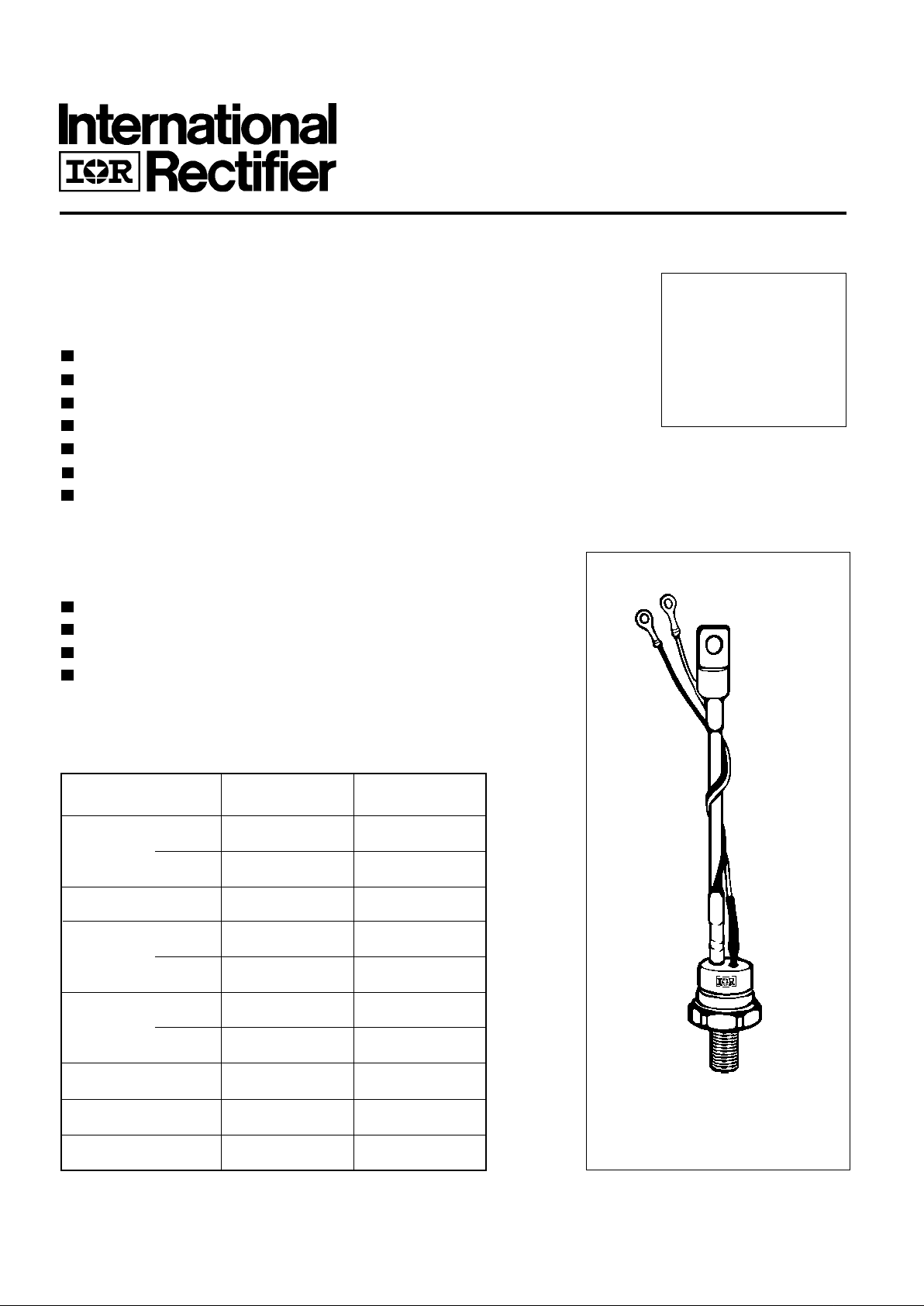
case style
TO-209AC (TO-94)
ST083S SERIES
INVERTER GRADE THYRISTORS
Stud V ersion
85A
Bulletin I25185/B
Page 2
ST083S Series
Voltage V
DRM/VRRM
, maximum V
RSM
, maximum I
DRM/IRRM
max.
Type number Code repetitive peak voltage non-repetitive peak voltage @ T
J
= TJ max.
VVmA
04 400 500
08 800 900
10 1000 1100
12 1200 1300
ELECTRICAL SPECIFICATIONS
Voltage Ratings
Frequency Units
50Hz 210 120 330 270 2540 1930
400Hz 200 120 350 210 1190 810
1000Hz 150 80 320 190 630 400 A
2500Hz 70 25 220 85 250 100
Recovery voltage Vr 50 50 50 50 50 50
Voltage before turn-on Vd V
DRM
V
DRM
V
DRM
Rise of on-state current di/dt 50 50 - - - - A/µs
Case temperature 60 85 60 85 60 85 °C
Equivalent values for RC circuit 22Ω / 0.15µF 22Ω / 0.15µF 22Ω / 0.15µF
I
TM
180oel
180
o
el
100µs
I
TM
I
TM
Current Carrying Capability
V
I
T(AV)
Max. average on-state current 85 A 180° conduction, half sine wave
@ Case temperature 85 °C
I
T(RMS)
Max. RMS on-state current 135 DC @ 77°C case temperature
I
TSM
Max. peak, one half cycle, 2450 t = 10ms No voltage
non-repetitive surge current 2560 A t = 8.3ms reapplied
2060 t = 10m s 100% V
RRM
2160 t = 8.3ms reapplied Sinusoidal half wave,
I
2
t Maximum I2t for fusing 30 t = 10ms No voltage Initial TJ = TJ max
27 t = 8.3ms reapplied
21 t = 10ms 100% V
RRM
19 t = 8.3ms reapplied
I
2
√t Maximum I2√t for fusing 300 KA2√s t = 0.1 to 10ms, no voltage reapplied
Parameter ST083S Units Conditions
On-state Conduction
KA2s
ST083S 30
Page 3
ST083S Series
V
TM
Max. peak on-state voltage 2.15 ITM= 300A, TJ = TJ max, tp = 10ms sine wave pulse
V
T(TO)1
Low level value of threshold
voltage
V
T(TO)2
High level value of threshold
voltage
r
t
1
Low level value of forward
slope resistance
r
t
2
High level value of forward
slope resistance
I
H
Maximum holding current 600 TJ = 25°C, IT > 30A
I
L
Typical latching current 1000 TJ = 25°C, VA= 12V, Ra = 6Ω, IG= 1A
Parameter ST083S Units Conditions
On-state Conduction
1.46 (16.7% x π x I
T(AV)
< I < π x I
T(AV)
), TJ = TJ max.
1.52 (I > π x I
T(AV)
), TJ = TJ max.
V
2.32 (16.7% x π x I
T(AV)
< I < π x I
T(AV)
), TJ = TJ max.
2.34 (I > π x I
T(AV)
), TJ = TJ max.
mΩ
mA
di/dt Max. non-repetitive rate of rise T
J
= TJ max, V
DRM
= rated V
DRM
of turned-on current I
TM
= 2 x di/dt
T
J
= 25°C, V
DM
= rated V
DRM, ITM
= 50A DC, tp= 1µs
Resistive load, Gate pulse: 10V, 5Ω source
T
J
= TJ max, I
TM
= 100A, commutating di/dt = 10A/µs
V
R
= 50V, tp = 200µs, dv/dt: see table in device code
Switching
Parameter ST083S Units Conditions
1000 A/µs
t
d
Typical delay time 0.80
µs
dv/dt Maximum critical rate of rise of T
J
= TJ max., linear to 80% V
DRM
, higher value
off-state voltage available on request
I
RRM
Max. peak reverse and off-state
I
DRM
leakage current
Parameter ST083S Units Conditions
Blocking
500 V/µs
30 mA TJ = TJ max, rated V
DRM/VRRM
applied
P
GM
Maximum peak gate power 40
P
G(AV)
Maximum average gate power 5
I
GM
Max. peak positive gate current 5 A TJ = TJ max, tp ≤ 5ms
+V
GM
Maximum peak positive
gate voltage
-V
GM
Maximum peak negative
gate voltage
I
GT
Max. DC gate current required
to trigger
V
GT
Max. DC gate voltage required
to trigger
I
GD
Max. DC gate current not to trigger 20 mA
V
GD
Max. DC gate voltage not to trigger 0.25 V
Triggering
Parameter ST083S Units Conditions
20
5
VTJ = TJ max, tp ≤ 5ms
200 mA
3V
T
J
= 25°C, VA = 12V, Ra = 6Ω
TJ = TJ max, rated V
DRM
applied
(*) t
q
= 10 to 20µs for 400 to 800V devices; tq = 15 to 30µs for 1000 to 1200V devices.
Min M a x
WT
J
= TJ max, f = 50Hz, d% = 50
t
q
Max. turn-off time (*) 10 3 0
Page 4

ST083S Series
1 - Thyristor
2 - Essential part number
3 - 3 = Fast turn off
4 - S = Compression bonding Stud
5 - Voltage code: Code x 100 = V
RRM
(See Voltage Ratings Table)
6 - P = Stud Base 1/2" 20UNF
7 - Reapplied dv/dt code (for tq Test Condition)
8 -tq code
9 - 0 = Eyelet terminals (Gate and Aux. Cathode Leads)
1 = Fast-on terminals (Gate and Aux. Cathode Leads)
2 = Flag terminals (For Cathode and Gate Terminals)
- Critical dv/dt:
None = 500V/µsec (Standard value)
L = 1000V/µsec (Special selection)
dv/dt - tq combinations available
dv/dt (V/µs) 20 50 100 200 400
t
q
(µs) 10 CN DN EN FN * HN
12 CM DM EM FM * HM
15 CL DL EL FL HL
18 CP DP EP FP * HP
20 CK DK EK FK * HK
t
q
(µs) 15 CL -- -- -- --
18 CP DP EP FP * --
20 CK DK EK FK * HK
25 CJ DJ EJ FJ HJ
30 -- DH EH FH HH
T
J
Max. junction operating temperature range -40 to 125
T
stg
Max. storage temperature range -40 to 150
R
thJC
Max. thermal resistance, junction to case 0.195 DC operation
R
thCS
Max. thermal resistance, case to heatsink 0.08 Mounting surface, smooth, flat and greased
T Mounting torque, ± 10% 15.5 Nm
(137) (Ibf-in)
14 Nm
(120) (Ibf-in)
wt Approximate weight 130 g
Case style TO-209AC (TO-94) See Outline Table
Parameter ST083S Units Conditions
Thermal and Mechanical Specifications
°C
K/W
Non lubricated threads
Lubricated threads
Ordering Information Table
5
6
8 9
ST 08 3 S 12 P F K 0
34
10
7
Device Code
12
∆R
thJC
Conduction
(The following table shows the increment of thermal resistence R
thJC
when devices operate at different conduction angles than DC)
180° 0.034 0.025
120° 0.041 0.042
90° 0.052 0.056 K/ W T
J
= TJ max.
60° 0.076 0.079
30° 0.126 0.127
Conduction angle Sinusoidal conduction Rectangular conduction Units Conditions
*Standard part number.
All other types available only on request.
only for
1000/1200V
up to 800V
10
Page 5

ST083S Series
Outline Table
Case Style TO-209AC (TO-94)
All dimensions in millimeters (inches)
Fast-on Terminals
C.S. 0.4 mm
2
10 (0.39)
RED SHRINK
RED CATHODE
RED SILICON RUBBER
4.3 (0.17) DIA
21 (0.83)
12.5 (0.49) MAX.
157 (6.18)
170 (6.69)
(.0006 s.i.)
8.5 (0.33) DIA.
16.5 (0.65) MAX.
MAX.
70 (2.75) MIN.
CERAMIC HOUSING
22.5 (0.88) MAX. DIA.
29 (1.14) MA X.
SW 27
C.S. 16mm
2
FLEXIBLE LEAD
(.025 s.i.)
2.6 (0.10) MAX.
WHITE SHRINK
2
0
(
0
.
7
9
)
M
I
N
.
29.5 (1.16)
MAX.
1/2"-20UNF-2A
9
.
5
(
0
.
3
7
)
M
I
N
.
WHITE GATE
215 (8.46)
Case Style TO-208AD (TO-83)
All dimensions in millimeters (inches)
10
1/2"-20UNF-2A
29.5 (1.16)
MAX.
MAX.
46 (1.81)
10
7.5
(0.30)
22.5 DIA.
16.5
(0.65)
12.5 (0.49)
5.2 (0.20) DIA.
29 (1.14)
(0.3 9)
(0.89) MAX.
21(0.83)
1.5 (0.06) DIA.
(0.39)
49 (1.93)
MAX.
CERAMIC HOUSING
FLAG TERMINALS
SW 27
2.4 (0.09)
AMP. 280000-1
REF-250
Page 6

ST083S Series
70
80
90
100
110
120
130
0 20 40 60 80 100 120 140
DC
30°
60°
90°
120°
180°
Average On- state Curr ent (A)
Max imu m Allowable Case Temperature (°C )
Conduction Peri od
ST08 3S Se ri e s
R (DC) = 0.19 5 K/W
thJC
Fig. 2 - Current Ratings CharacteristicsFig. 1 - Current Ratings Characteristics
Fig. 3 - On-state Power Loss Characteristics
Fig. 4 - On-state Power Loss Characteristics
80
90
100
110
120
130
0 102030405060708090
Maxi mum Allowable Case Temperature (° C)
30°
60°
90°
120°
180°
Aver age On-state Current (A)
Conduction Angle
ST083S Series
R (DC) = 0.195 K/ W
thJC
25 50 75 100 125
M aximu m Al lowable A m bient Temperature ( °C)
R
=
0
.
1
K
/
W
-
D
e
l
t
a
R
t
h
S
A
0
.
2
K
/
W
0
.
3
K
/
W
0
.
4
K
/
W
0
.
5
K
/
W
0
.
8
K
/
W
1
.
2
K
/
W
0
50
100
150
200
250
0 20 40 60 80 100 120 140
DC
180°
120°
90°
60°
30°
RMS Lim it
Conduction P er i od
Max imum A ve rage On -state Power Loss (W)
Average On-state Cur rent (A)
ST083S Series
T = 125°C
J
25 50 75 100 125
Maxi mu m Allowable Ambient Temperature (° C)
R
=
0
.
1
K
/
W
-
D
e
l
t
a
R
t
h
S
A
0
.
2
K
/
W
0
.
3
K/
W
0
.
4
K
/
W
0
.
5
K
/
W
0
.
8
K
/
W
1
.
2
K
/
W
0
20
40
60
80
100
120
140
160
180
0
10 20 30 40 50 60 70 80 90
180°
120°
90°
60°
30°
RMS Limit
Conduction Angle
M ax i m u m A v erage On-s tat e Power Loss (W)
Average On-state Current (A)
ST083S Series
T = 12 5°C
J
Page 7

ST083S Series
Fig. 9 - Reverse Recovered Charge Characteristics Fig. 10 - Reverse Recovery Current Characteristics
Fig. 7 - On-state Voltage Drop Characteristics Fig. 8 - Thermal Impedance Z
thJC
Characteristic
Fig. 5 - Maximum Non-repetitive Surge Current
Fig. 6 - Maximum Non-repetitive Surge Current
1000
1200
1400
1600
1800
2000
2200
1 10 100
Number Of Equal Amplitude Half Cycle Current Pulses (N)
Peak Half Sine W ave On-state Cur r ent (A)
Initial T = 125°C
@ 60 H z 0.0083 s
@ 50 H z 0.0100 s
J
ST 083S Series
At Any Rated Load Con dition And Wi th
Rated V Applied Follo w ing Surge.
RRM
1000
1200
1400
1600
1800
2000
2200
2400
2600
0.01 0.1 1
P u lse T r ain Du ration (s )
Versus P ulse Train Du ration. Control
Of C o ndu cti o n May No t Be Main tained.
Peak Half Sine W ave On-state Cur r ent (A)
Ini tial T = 125 °C
N o V oltage Reappl i e d
Rated V Reapplied
RRM
J
S T083S Se r ie s
Max imum Non Repetitive Sur ge C u r r en t
100
1000
10000
11.522.533.544.555.566.5
T = 25°C
J
I ns tan tane ous On-state Current (A)
Instantaneous On-state Voltage (V)
T = 125°C
J
ST 083S Se rie s
0. 01
0. 1
1
0. 001 0. 01 0.1 1 10
Square Wave Pulse Duration (s)
thJC
Transient Thermal I mpedance Z (K/W)
ST0 83S Series
Steady State Valu e
R = 0 .195 K/W
(DC Operation)
thJC
10
20
30
40
50
60
70
80
90
100
110
120
10 20 30 40 50 60 70 80 90 100
Maximum Reverse Recovery Current - I rr (A )
Rate Of Fall Of Forward Current - di/dt (A/µs)
ST 083S Series
T = 125 °C
I = 500 A
300 A
200 A
J
100 A
50 A
TM
20
40
60
80
100
120
140
160
10 20 30 40 50 60 70 80 90 100
ST083S Se rie s
T = 125 °C
I = 500 A
300 A
200 A
J
100 A
50 A
Rate Of Fall Of On -state Cu rren t - di/dt (A /µs)
M axi m um Rev erse Recov ery Ch arge - Q rr (µ C)
TM
Page 8

ST083S Series
Fig. 13 - Frequency Characteristics
Fig. 11 - Frequency Characteristics
Fig. 12 - Frequency Characteristics
1E 1
1E 2
1E 3
1E 4
1E11E21E31E4
50 Hz
400
2500
100
Pulse Basewidth (µs )
P eak On-state Cur rent (A)
1000
1500
2000
3000
200
500
Snubber circuit
R = 2 2 ohms
C = 0.15 µF
V = 80% V
s
s
D
DRM
ST0 83S Se rie s
Sin u soidal pulse
T = 60°C
C
1E 4
tp
1E1 1E2 1E3 1E4
50 H z
400
2500
100
Pulse Ba se wid th (µs)
1000
1500
2000
3000
200
500
Snubb er circuit
R = 22 ohms
C = 0.15 µF
V = 80% V
s
s
D
DRM
ST083S Se ri es
Sin usoidal pul se
T = 85 °C
C
tp
1E 1
1E 1
1E 2
1E 3
1E 4
1E 1 1E2 1E 3 1E 4
50 Hz
400
2500
100
1000
1500
2000
3000
200
500
Snubber cir cuit
R = 22 ohms
C = 0.15 µF
V = 80% V
s
s
D
DRM
ST083S Series
Trape zoidal pu lse
T = 60 °C
di/dt = 50A/µs
C
Pulse Ba se wid t h (µs)
Peak On-state Current (A)
tp
1E4
1E1 1E2 1E3 1E4
50 Hz
400
2500
100
Pulse Basew id th ( µs)
1000
1500
2000
200
500
Snubber circuit
R = 22 ohms
C = 0.15 µF
V = 80% V
s
s
D
DRM
ST08 3S S eries
Trape zoidal pu lse
T = 8 5°C
di /dt = 50A/µs
C
tp
1E1
1E 1
1E 2
1E 3
1E 4
1E 1 1E2 1E3 1E 4
400
2500
100
1000
1500
2000
3000
200
500
Snubber circuit
R = 2 2 ohms
C = 0.15 µF
V = 80% V
s
s
D
DRM
ST0 83 S Se rie s
Trape zoi dal pulse
T = 60°C
di/dt = 100A/µs
C
Pulse Ba se width (µs)
P eak On-state Current (A)
tp
1E4
50 Hz
1E1 1E2 1E3 1E4
50 Hz
400
2500
100
Pulse Ba sewidth (µs)
1000
1500
2000
200
500
Snubber circuit
R = 22 ohms
C = 0.15 µF
V = 80% V
s
s
D
DRM
ST083S Se ri e s
Trapezoidal pulse
T = 85°C
di/dt = 100A/µs
C
tp
1E1
Page 9

ST083S Series
Fig. 14 - Maximum On-state Energy Power Loss Characteristics
Fig. 15 - Gate Characteristics
0.1
1
10
100
0.001 0.01 0.1 1 10 100
VGD
IGD
(b)
(a)
Tj=25 ° C
Tj=125 °C
Tj=-40 °C
(1)
(2)
I nstantaneous Gate Current (A)
Instantaneous Gate Voltage (V)
Rectangular gate pulse
a) Recommended load line for
b) Recommended load line for
<=30% rated di/dt : 10V, 10ohms
rated di/dt : 20V, 10ohms; tr<=1 µs
tr<=1 µs
(1) PGM = 10W, tp = 20ms
(2) PGM = 20W, tp = 10ms
(3) PGM = 40W, tp = 5ms
(4) PGM = 60W, tp = 3.3ms
(3)
Device: ST083S Series
(4)
Frequency Limited by PG(AV)
1E 1
1E 2
1E 3
1E 4
1E 1 1E 2 1E 3 1E 4
Pulse Basewidth (µ s)
20 joules per pulse
2
1
0.5
0.3
0.2
0.1
ST083S Series
Sinusoidal pulse
10
5
Peak On-state Curr ent (A)
3
tp
1E 4 1E1 1E 2 1E 3 1E 4
Pulse Basew idth (µs)
ST083S Se ri es
Rectangular pulse
di/dt = 50A/µs
20 joules per pulse
7.5
4
2
1
0.5
0.3
0.2
0.1
tp
1E1
 Loading...