

Page 1
PAD/JPAD/SSTPAD Series
Part Numb
I
A)
Low-Leakage Pico-Amp Diodes
PAD1 JPAD5 SSTPAD5
PAD5 JPAD50 SSTPAD100
PAD50
Product Summary
er
PAD1 –1
PAD5/JPAD5/SSTPAD5 –5
PAD50/JPAD50 –50
SSTPAD100 –100
Max (p
R
Features Benefits Applications
Ultralow Leakage: PAD1 <1 pA
Ultralow Capacitance: PAD1 <0.8 pF
Two-Leaded Package
Negligible Circuit Leakage Contribution
Circuit “Transparent” Except to Shunt
High-Frequency Spikes
Simplicity of Operation
Op Amp Input Protection
Multiplexer Overvoltage
Protection
Description
The PAD/JPAD/SSTPAD series of extremely low-leakage
diodes provides a superior alternative to conventional diode
technology when reverse current (leakage) must be
minimized. They feature leakage currents ranging from
–1 pA (PAD1) to –100 pA (SSTPAD100) to support a wide
range of applications. These devices are well suited for use
in applications such as input protection for operational
amplifiers.
The hermetically sealed TO-206AF (TO-72) package
allows full military processing per MIL-S-19500 (see
Military Information). The TO-226A (TO-92) plastic
package provides a low-cost option. The TO-236
(SOT-23) package provides surface-mount capability.
Both J and SST series are available in tape-and-reel for
automated assembly. (See Packaging Information.)
Updates to this data sheet may be obtained via facsimile by calling Siliconix FaxBack, 1-408-970-5600. Please request FaxBack document #70339.
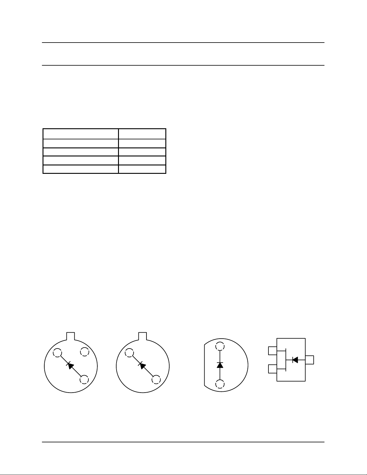
TO-206AF (TO-72)
Modified
C
1
Top View
PAD1
PAD5
Case
3
2
A
Siliconix
S-52424—Rev. G, 14-Apr-97
TO-206AA (TO-18)
Modified
C
1
Top View
PAD50
2
A and Case
TO-226AA (TO-92)
Modified
C
A
1
2
Top View
JPAD5
JPAD50
TO-236
(SOT-23)
C
1
C
2
Top View
SSTPAD5 (05)*
SSTPAD100 (01)
*Marking Code for TO-236
A
3
1
Page 2
PAD/JPAD/SSTPAD Series
Reverse Current
IRV
V
pA
V
Reverse Capacitance
CRV
R
MHz
pF
Absolute Maximum Ratings
Forward Current: (PAD 50 mA. . . . . . . . . . . . . . . . . . . . . .
(JPAD/SSTPAD ) 10 mA. . . . . . . . . . . . .
Total Device Dissipation: (PAD)
Operation Junction Temp: (PAD) –55 to 175_C. . . . . . . . . . . . . . . .
Specifications
b
(JPAD/SSTPAD)
(JPAD/SSTPAD )
a
b
c
a
–55 to 150_C. . . . . .
Parameter Symbol Test Conditions Min TypbMax Unit
Static
R
Reverse Breakdown Voltage BV
Forward Voltage Drop V
R
F
IR = –1 A
300 mW. . . . . . . . . . . . . . . . . . .
350 mW. . . . . . . . . .
= –20
1
Lead Temperature (
Notes:
a. T
= 25_C unless otherwise noted.
A
b. Derate 2 mW/_C above 25_C.
c. Derate 2.8 mW/_C above 25_C.
/16” from case for 10 sec.) 300_C. . . . . . . . . . . . .
Limits
PAD1
PAD5/JPAD5/SSTPAD5 –1
PAD50/JPAD50 –5
SSTPAD100 –10
PAD1/PAD5 –45 –60
SSTPAD5/100 –30 –55
All Others –35 –55
IF = 1 mA 0.8 1.5
–0.3
–1
–5
–50
–100
Dynamic
–
= –5V, f = 1
Notes:
a. T
= 25_C unless otherwise noted. NT/NPA
A
b. Typical values are for DESIGN AID ONLY, not guaranteed nor subject to production testing.
PAD1/PAD5 0.5 0.8
All Others 1.5 2
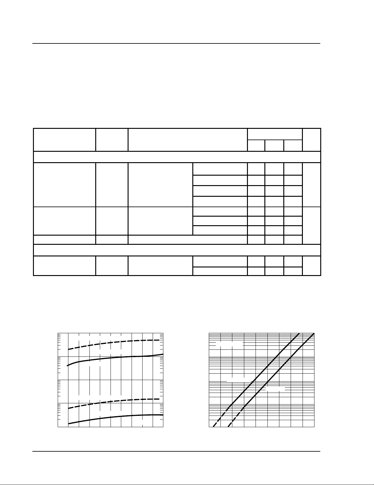
Typical Characteristics
–1000
(pA)
R
I
–100
–10
–1
–0.1
Reverse Current vs. Reverse Voltage
PAD/JPAD/SSTPAD5
IR @ 125_C
PAD1
PAD/JPAD/SSTPAD5
IR @ 25_C
0
–6 –12 –18 –24 –30
VR (V) TA – Temperature (_C)
PAD1
(pA)
R
I
–0.01
–100
–10
–1
–0.1
Reverse Current vs. Temperature
VR = –20 V
All Others
PAD1/5
–55 –35 125
–15 5 25 45 65 85 105
2 Siliconix
S-52424—Rev. G, 14-Apr-97
Page 3

 Loading...