

Page 1
High End, Multichannel,
a
32-Bit Floating-Point Audio Processor
FEATURES
Super Harvard Architecture Computer (SHARC)
4 Independent Buses for Dual Data, Instruction, and
I/O Fetch on a Single Cycle
32-Bit Fixed-Point Arithmetic; 32-Bit and 40-Bit Floating
Point Arithmetic
544 Kbits On-Chip SRAM Memory, Integrated I/O
Peripheral I
Transmit
2
S Support for
Channels
8 Simultaneous Receive and
66 MIPS, 198 MFLOPS Peak, 132 MFLOPS Sustained
Performance
User-Configurable 544 Kbits On-Chip SRAM Memory
2 External Port, DMA Channels and 8 Serial Port,
DMA Channels
Decodes Industry Standard Formats Using a 32-Bit
Floating Point Implementation for Decoding
®
Digital AC-3, Dolby Digital EX Processing
Dolby
Dolby Pro Logic
®
, 96 kHz, Dolby Pro Logic II
Dolby Headphone, Dolby 3/0
DTS® 5.1, DTS-ES®-Discreet 6.1, DTS Matrix and Matrix 3.0,
DTS 96/24®, DTS NEO:6
®
THX
Ultra, Select, Ultra2, 5.1, 7.1, EX
®
Labs Circle Surround IITM, Virtual Loudspeaker
SRS
MPEG AAC, MPEG2 Decode, MPEG 2-Channel Decode
PCM, PCM 96 kHz
HDCD, MLP*
Delay 7.1, 96 kHz
Bass 7.1, 96 kHz, Bass/Treble 2 Channel
ADI Surround: Club, Music, and Stadium
AAC (LC), AAC (LC) 2 Channel, AAC MP
WaveSurround 5.1 Channel to Headphone, Stereo to
Headphone, Channel to Loudspeaker, Stereo to
Loudspeaker
Downsampling 96 kHz to 48 kHz (2-Channel)
3-Band Equalizer, 2-Channel
Encoders: AC-3 2-Channel Consumer Encoder
Single Chip DSP-Based Implementation of Digital Audio
Algorithms
2
S Compatible Ports
I
Interface to External SDRAM
®
SST-Melody®-SHARC
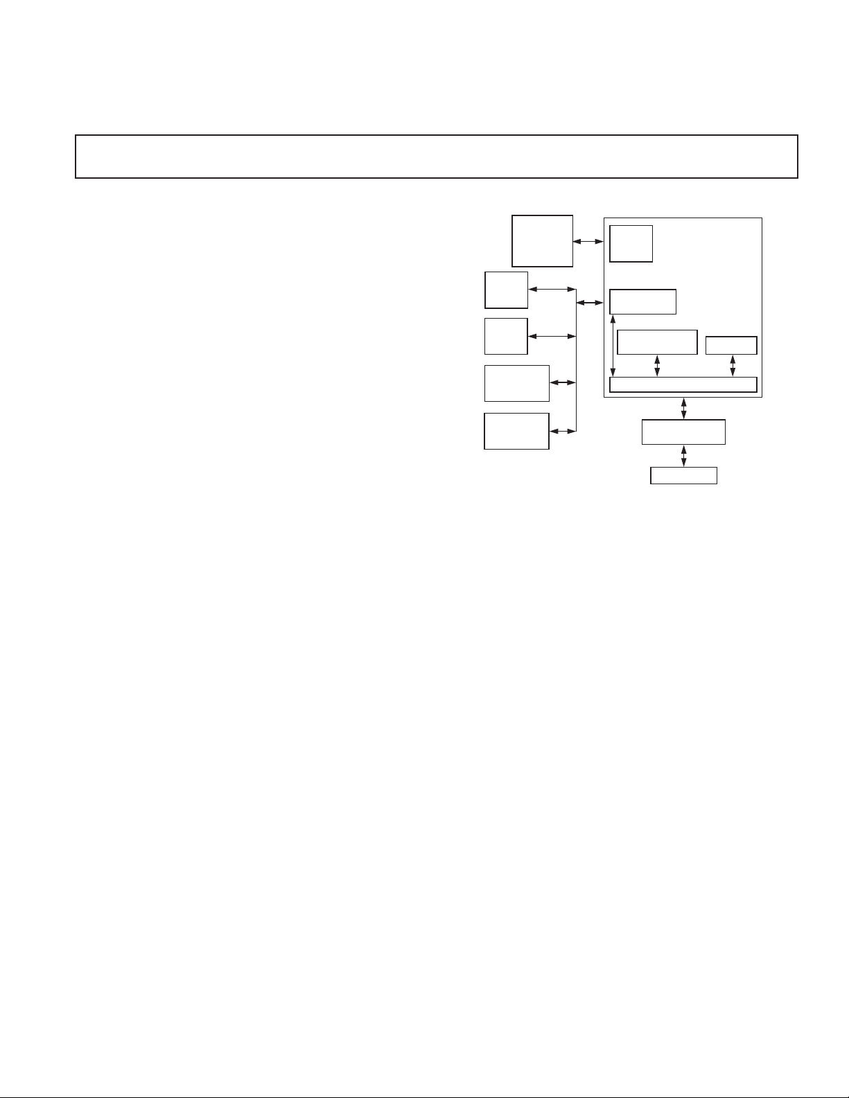
FUNCTIONAL BLOCK DIAGRAM
SDRAM
128K ⴛ 32,
BOOT ROM
-
1M ⴛ 8
ADC
DAC
S/PDIF
TRANSMITTER
S/PDIF
RECEIVER
Easy Interfaces to Audio Codecs
96 kHz Processing
Supports Customer Specific Post Processing
Automatic Stream Detection and Code Loading
Easy to Use Software Architecture
Optimized Library of Routines
Host Communication Using 16-Bit Parallel Port or SPI Port
Highly Flexible Serial Ports
SRAM Interface for More Delay
Supports IEC60958 For Bit Streams
8-Channel Output Using TDM Codecs
APPLICATIONS
Home Theater AVR Systems
Automotive Audio Receivers
Video Game Consoles
DVD Players
Cable and Satellite Set-Top Boxes
Multimedia Audio/Video Gateways
IRQ
GPIO
SST-Melody-SHARC
SERIAL PORT
ALGORITHMS
KERNEL
DMA CONNECTION
OR DUAL BUFFER
HOST MICRO
COMMAND
Melody and SHARC are registered trademarks of Analog Devices, Inc.
DTS, DTS-ES, and DTS 96/24 are registered trademarks of Digital Theater
Systems, Inc.
Dolby and Pro Logic are registered trademarks of Dolby Laboratories
Licensing Corporation.
SRS is a registered trademark and Circle Surround II is a trademark of SRS Labs.
THX is a registered trademark of the THX, Ltd.
*MLP is implemented, not certified.
REV. 0
Information furnished by Analog Devices is believed to be accurate and
reliable. However, no responsibility is assumed by Analog Devices for its
use, nor for any infringements of patents or other rights of third parties that
may result from its use. No license is granted by implication or otherwise
under any patent or patent rights of Analog Devices.
GENERAL DESCRIPTION
The SST-Melody-SHARC family of powerful 32-bit Audio Processors
from Analog Devices provides flexible solutions and delivers
a host of features across high end and high fidelity audio systems
to the AV receiver and DVD markets. It includes multichannel
audio decoders, encoders, and post processors for digital
audio designs using DSP chipsets in home theater systems and
automotive audio receivers.
(continued on page 11)
One Technology Way, P.O. Box 9106, Norwood, MA 02062-9106, U.S.A.
Tel: 781/329-4700 www.analog.com
Fax: 781/326-8703 © Analog Devices, Inc., 2002
Page 2
SST-Melody-SHARC–SPECIFICATIONS
RECOMMENDED OPERATING CONDITIONS
1
Test C Grade K Grade
Parameter Conditions Min Max Min Max Unit
V
DD
T
CASE
V
IH
V
IL1
V
IL2
NOTES
1
See Environmental Conditions section for information on thermal specifications.
2
Applies to input and bidirectional pins: DATA31–0, ADDR23–0, BSEL, RD, WR, SW, ACK, SBTS, IRQ2–0, FLAG11–0, HBG, CS, DMAR1, DMAR2, BR2–1, ID2–0,
RPBA, CPA, TFS0, TFS1, RFS0, RFS1, BMS, TMS, TDI, TCK, HBR, DR0A, DR1A, DR0B, DR1B, TCLK0, TCLK1, RCLK0, RCLK1, RESET, TRST,
PWM_EVENT0, PWM_EVENT1, RAS, CAS , SDWE, SDCKE.
3
Applies to input pin CLKIN.
Supply Voltage 3.13 3.60 3.13 3.60 V
Case Operating Temperature –40 +100 0 +85 °C
High Level Input Voltage @ VDD = max 2.0 VDD + 0.5 2.0 VDD + 0.5 V
Low Level Input Voltage2@ VDD = min –0.5 +0.8 –0.5 +0.8 V
Low Level Input Voltage3@ VDD = min –0.5 +0.7 –0.5 +0.7 V
ELECTRICAL CHARACTERISTICS
C and K Grades
Parameter Test Conditions Min Max Unit
3
4
1
3
1
5, 6, 7, 8
5
6
9
8
7
@ VDD = min, IOH = –2.0 mA
@ VDD = min, IOL = +4.0 mA
@ VDD = max, VIN = VDD max 10 µA
@ VDD = max, VIN = 0 V 10 µA
@ VDD = max, VIN = 0 V 150 µA
@ VDD = max, VIN = VDD max 10 µA
@ VDD = max, VIN = 0 V 8 µA
@ VDD = max, VIN = 0 V 150 µA
@ VDD = max, VIN = 1.5 V 350 µA
@ VDD = max, VIN = 0 V 4 mA
@ VDD = max, VIN = 0 V 1.5 mA
fIN = 1 MHz, T
= 25°C, VIN = 2.5 V 8 pF
CASE
V
OH
V
OL
I
IH
I
IL
I
ILP
I
OZH
I
OZL
I
OZLS
I
OZLA
I
OZLAR
I
OZLC
C
IN
NOTES
1
Applies to output and bidirectional pins: DATA31–0, ADDR 23–0, MS3–0, RD, WR, SW, ACK, FLAG11–0, HBG, REDY, DMAG1, DMAG2, BR2–1, CPA,
TCLK0, TCLK1, RCLK0, RCLK1, TFS0, TFS1, RFS0, RFS1, DT0A, DT1A, DT0B, DT1B, XTAL, BMS, TDO, EMU, BMSTR, PWM_EVENT0,
PWM_EVENT1, RAS, CAS, DQM, SDWE, SDCLK0, SDCLK1, SDCKE, SDA10.
2
See Output Drive Current section for typical drive current capabilities.
3
Applies to input pins: ACK, SBTS, IRQ2–0, HBR, CS, DMAR1, DMAR2, ID1–0, BSEL, CLKIN, RESET , TCK (Note that ACK is pulled up internally with 2 k Ω
during reset in a multiprocessor system, when ID1–0 = 01 and another SST-Melody-SHARC is not requesting bus mastership).
4
Applies to input pins with internal pull-ups: DR0A, DR1A, DR0B, DR1B, TRST, TMS, TDI.
5
Applies to three-statable pins: DATA31–0, ADDR 23–0, MS3–0, RD, WR, SW, ACK, FLAG11–0, REDY, HBG, DMAG1, DMAG2, BMS, TDO, RAS, CAS,
DQM, SDWE, SDCLK0, SDCLK1, SDCKE, SDA10, and EMU (note that ACK is pulled up internally with 2 kΩ during reset in a multiprocessor system,
when ID1–0 = 01 and another SST-Melody-SHARC is not requesting bus mastership).
6
Applies to three-statable pins with internal pull-ups: DT0A, DT1A, DT0B, DT1B, TCLK0, TCLK1, RCLK0, RCLK1.
7
Applies to CPA pin.
8
Applies to ACK pin when pulled up.
9
Applies to ACK pin when keeper latch enabled.
10
Guaranteed but not tested.
11
Applies to all signal pins.
Specifications subject to change without notice.
High Level Output Voltage
Low Level Output Voltage
High Level Input Current
Low Level Input Current
Low Level Input Current
Three-State Leakage Current
Three-State Leakage Current
Three-State Leakage Current
Three-State Leakage Current
Three-State Leakage Current
Three-State Leakage Current
Input Capacitance
10, 11
2
2
2.4 V
0.4 V
REV. 0–2–
Page 3
SST-Melody-SHARC
ABSOLUTE MAXIMUM RATINGS*
Supply Voltage . . . . . . . . . . . . . . . . . . . . . . . . –0.3 V to +4.6 V
Input Voltage . . . . . . . . . . . . . . . . . . . . . –0.5 V to V
Output Voltage Swing . . . . . . . . . . . . . . –0.5 V to V
Load Capacitance . . . . . . . . . . . . . . . . . . . . . . . . . . . . 200 pF
Junction Temperature Under Bias . . . . . . . . . . . . . . . . . 130°C
Storage Temperature Range . . . . . . . . . . . . . –65°C to +150°C
Lead Temperature (5 seconds) . . . . . . . . . . . . . . . . . . . . 280°C
*Stresses greater than those listed under Absolute Maximum Ratings may cause
permanent damage to the device. These are stress ratings only; functional operation of the device at these or any other conditions greater than those indicated in
the operational sections of this specification is not implied. Exposure to absolute
maximum rating conditions for extended periods may affect device reliability.
Case Temperature Instruction On-Chip Operating Package
Part Number Range Rate (MHz) SRAM (Kbit) Voltage (V) Options
ADSST-21065LKS-240 0°C to 85°C60 544 3.3 S-208-2
ADSST-21065LCS-240 –40°C to +100°C60 544 3.3 S-208-2
ADSST-21065LKCA-240 0°C to 85°C60 544 3.3 BC-196
ADSST-21065LKS-264 0°C to 85°C66 544 3.3 S-208-2
ADSST-21065LKCA-264 0°C to 85°C66 544 3.3 BC-196
+ 0.5 V
DD
+ 0.5 V
DD
ORDERING GUIDE
CAUTION
ESD (electrostatic discharge) sensitive device. Electrostatic charges as high as 4000 V readily
accumulate on the human body and test equipment and can discharge without detection. Although the
SST-Melody-SHARC features proprietary ESD protection circuitry, permanent damage may occur
on devices subjected to high energy electrostatic discharges. Therefore, proper ESD precautions are
recommended to avoid performance degradation or loss of functionality.
REV. 0
–3–
Page 4
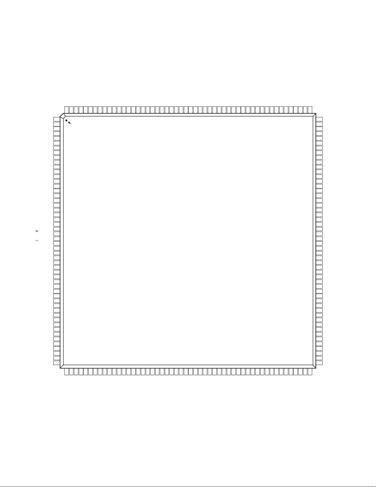
SST-Melody-SHARC
208-LEAD MQFP PIN CONFIGURATIONS
PWM
PWM
VDD
RSF0
GND
RCLK0
DR0A
DR0B
TFS0
TCLK0
VDD
GND
DT0A
DT0B
RFS1
GND
RCLK1
DR1A
DR1B
TFS1
TCLK1
VDD
VDD
DT1A
DT1B
EVENT1
GND
EVENT0
BR1
BR2
VDD
CLKIN
XTAL
VDD
GND
SDCLK1
GND
VDD
SDCLK0
DMAR1
DMAR2
HBR
GND
RAS
CAS
SDWE
VDD
DQM
SDCKE
SDA10
GND
DMAG1
DMAG2
HBG
NC
IRQ2
IRQ1
208
207
206
1
2
PIN 1
IDENTIFIER
3
4
5
6
7
8
9
10
11
12
13
14
15
16
17
18
19
20
21
22
23
24
25
26
27
28
29
30
31
32
33
34
35
36
37
38
39
40
41
42
43
44
45
46
47
48
49
50
51
52
535455565758596061
CS
VDD
BMSTR
IRQ0
205
SBTS
GND
204
GND
VDD
NCNCFLAG3
203
202
201
200
RD
WR
VDD
GND
FLAG2
FLAG1
FLAG0
ADDR0
ADDR1
GND
199
198
197
196
195
194
62636465666768
SW
CPA
VDD
GND
REDY
VDD
VDD
ADDR2
193
192
69
ACK
GND
VDD
ADDR3
ADDR4
ADDR5
191
188
190
189
ADSST-21065L
73747576777879
71
72
70
MS0
MS1
GND
GND
GND
186
185
184
ADDR8
183
182
GND
187
VDD
ADDR6
ADDR7
OO
TOP VIEW
(Not to Scale)
MS2
MS3
VDD
FLAG9
FLAG11
FLAG10
NC = NO CONNECT
ADDR10
ADDR11
GND
178
177
179
DATA0
DATA1
DATA2
VDD
176
VDD
ADDR12
ADDR13
ADDR14
175
174
173
DATA3
DATA4
DATA5
ADDR9
GND
181
180
80
8182838486878889908591
GND
FLAG8
VDD
ADDR15
ADDR16
ADDR17
172
171
170
169
92939496979899
GND
DATA6
DATA7
DATA8
GND
168
VDD
ADDR18
GND
167
166
95
VDD
GND
VDD
ADDR19
ADDR20
165
164
163
DATA9
DATA10
ADDR21
ADDR22
162
161
100
GND
DATA11
ADDR23
GND
160
159
101
102
DATA12
DATA13
NC
VDD
158
103
NC
RESET
157
156
155
154
153
152
151
150
149
148
147
146
145
144
143
142
141
140
139
138
137
136
135
134
133
132
131
130
129
128
127
126
125
124
123
122
121
120
119
118
117
116
115
114
113
112
111
110
109
108
107
106
105
104
DATA14
VDD
GND
GND
BMS
BSEL
TCK
GND
TMS
TDI
TRST
TDO
EMU
ID0
ID1
NC
VDD
VDD
GND
FLAG4
FLAG5
FLAG6
GND
FLAG7
DATA31
DATA30
VDD
VDD
GND
DATA29
DATA28
DATA27
GND
VDD
DATA26
DATA25
DATA24
VDD
GND
DATA23
DATA22
DATA21
NC
GND
DATA20
DATA19
DATA18
VDD
DATA17
DATA16
DATA15
GND
VDD
REV. 0–4–
Page 5
SST-Melody-SHARC
196-BALL CSPBGA PIN CONFIGURATION
14 13 12 11 10 9 8 7 6 5 4 3 2 1
NC7
TCK
TDO
EMU
FLAG4
FLAG7
DATA29
DATA26
DATA23
DATA22
DATA18
DATA15
NC8
GND
BSEL
TRST
ID1
FLAG5
DATA30
DATA27
DATA25
DATA20
DATA17
DATA14
ADDR18
ADDR23
RESET
TMS
TDI
FLAG6
DATA31
DATA28
DATA24
DATA21
DATA16
DATA12
ADDR17
ADDR21
ADDR22
BMS
ID0
VDD
VDD
VDD
VDD
DATA19
DATA13
DATA9
ADDR14
ADDR19
ADDR20
VDD
VDD
GND
GND
GND
GND
VDD
DATA8
DATA5
ADDR11
ADDR15
ADDR16
VDD
GND
GND
GND
GND
GND
GND
VDD
DATA2
ADDR8
ADDR12
ADDR13
VDD
GND
GND
GND
GND
GND
GND
VDD
FLAG10
ADDR7
ADDR9
ADDR10
VDD
GND
GND
GND
GND
GND
GND
VDD
ACK
ADDR6
ADDR5
ADDR4
VDD
GND
GND
GND
GND
GND
GND
VDD
CPA
ADDR3
ADDR2
ADDR1
FLAG1
VDD
GND
GND
GND
GND
VDD
VDD
RD
ADDR0
FLAG0
FLAG3
IRQ1
RFS1
VDD
VDD
VDD
VDD
SDWE
DMAG2
CS
FLAG2
IRQ0
IRQ2
DR0B
DT0A
DR1A
DT1A
BR2
SDCLK1
HBR
SDA10
DMAG1
NC2
RFS0
RCLK0
TFS0
DT0B
DR1B
DT1B
BR1
XTAL
SDCLK0
CAS
SDCKE
NC1
DR0A
TCLK0
RCLK1
TFS1
TCLK1
PWM_
EVENT1
PWM_
EVENT0
CLKIN
DMAR1
DMAR2
RAS
A
B
C
D
E
F
G
H
J
K
L
M
NC6
NC5
DATA11
DATA6
DATA10
DATA3
DATA7
DATA0
DATA4
FLAG8
DATA1
FLAG9
FLAG11
MS3
MS1
MS2
GND
MS0
REDY
SW
SBTS
WR
BMSTR
GND
HBG
NC4
DQM
NC3
N
P
REV. 0
–5–
Page 6
SST-Melody-SHARC
208-LEAD MQFP PIN CONFIGURATION
Pin No. Mnemonic Pin No. Mnemonic Pin No. Mnemonic Pin No. Mnemonic
1 V
DD
2 RFS0
3GND
4 RCLK0
5 DR0A
6 DR0B
7 TFS0
8 TCLK0
9V
DD
10 GND
11 DT0A
12 DT0B
13 RFS1
14 GND
15 RCLK1
16 DR1A
17 DR1B
18 TFS1
19 TCLK1
20 V
21 V
DD
DD
22 DT1A
23 DT1B
24 PWM_EVENT1
25 GND
26 PWM_EVENT0
27 BR1
28 BR2
29 V
DD
30 CLKIN
31 XTAL
32 V
DD
33 GND
34 SDCLK1
35 GND
36 V
DD
37 SDCLK0
38 DMAR1
39 DMAR2
40 HBR
41 GND
42 RAS
43 CAS
44 SDWE
45 V
DD
46 DQM
47 SDCKE
48 SDA10
49 GND
50 DMAG1
51 DMAG2
52 HBG
53 BMSTR
54 V
DD
55 CS
56 SBTS
57 GND
58 WR
59 RD
60 GND
61 V
DD
62 GND
63 REDY
64 SW
65 CPA
66 V
67 V
DD
DD
68 GND
69 ACK
70 MS0
71 MS1
72 GND
73 GND
74 MS2
75 MS3
76 FLAG11
77 V
DD
78 FLAG10
79 FLAG9
80 FLAG8
81 GND
82 DATA0
83 DATA1
84 DATA2
85 V
DD
86 DATA3
87 DATA4
88 DATA5
89 GND
90 DATA6
91 DATA7
92 DATA8
93 V
DD
94 GND
95 V
DD
96 DATA9
97 DATA10
98 DATA11
99 GND
100 DATA12
101 DATA13
102 NC
103 NC
104 DATA14
105 V
DD
106 GND
107 DATA15
108 DATA16
109 DATA17
110 V
DD
111 DATA18
112 DATA19
113 DATA20
114 GND
115 NC
116 DATA21
117 DATA22
118 DATA23
119 GND
120 V
DD
121 DATA24
122 DATA25
123 DATA26
124 V
DD
125 GND
126 DATA27
127 DATA28
128 DATA29
129 GND
130 V
131 V
DD
DD
132 DATA30
133 DATA31
134 FLAG7
135 GND
136 FLAG6
137 FLAG5
138 FLAG4
139 GND
140 V
141 V
DD
DD
142 NC
143 ID1
144 ID0
145 EMU
146 TDO
147 TRST
148 TDI
149 TMS
150 GND
151 TCK
152 BSEL
153 BMS
154 GND
155 GND
156 V
DD
157 RESET
158 V
DD
159 GND
160 ADDR23
161 ADDR22
162 ADDR21
163 V
DD
164 ADDR20
165 ADDR19
166 ADDR18
167 GND
168 GND
169 ADDR17
170 ADDR16
171 ADDR15
172 V
DD
173 ADDR14
174 ADDR13
175 ADDR12
176 V
DD
177 GND
178 ADDR11
179 ADDR10
180 ADDR9
181 GND
182 V
DD
183 ADDR8
184 ADDR7
185 ADDR6
186 GND
187 GND
188 ADDR5
189 ADDR4
190 ADDR3
191 V
192 V
DD
DD
193 ADDR2
194 ADDR1
195 ADDR0
196 GND
197 FLAG0
198 FLAG1
199 FLAG2
200 V
DD
201 FLAG3
202 NC
203 NC
204 GND
205 IRQ0
206 IRQ1
207 IRQ2
208 NC
REV. 0–6–
Page 7

SST-Melody-SHARC
196-BALL CSPBGA PIN CONFIGURATION
Ball No. Mnemonic Ball No. Mnemonic Ball No. Mnemonic Ball No. Mnemonic Ball No. Mnemonic
A1 NC1 B1 DR0A C1 TCLK0 D1 RCLK1 E1 TFS1
A2 NC2 B2 RFS0 C2 RCLK0 D2 TFS0 E2 DT0B
A3 FLAG2 B3 IRQ0 C3 IRQ2 D3 DR0B E3 DT0A
A4 ADDR0 B4 FLAG0 C4 FLAG3 D4 IRQ1 E4 RFS1
A5 ADDR3 B5 ADDR2 C5 ADDR1 D5 FLAG1 E5 V
A6 ADDR6 B6 ADDR5 C6 ADDR4 D6 V
A7 ADDR7 B7 ADDR9 C7 ADDR10 D7 V
A8 ADDR8 B8 ADDR12 C8 ADDR13 D8 V
A9 ADDR11 B9 ADDR15 C9 ADDR16 D9 V
A10 ADDR14 B10 ADDR19 C10 ADDR20 D10 V
DD
DD
DD
DD
DD
E6 GND
E7 GND
E8 GND
E9 GND
E10 V
A11 ADDR17 B11 ADDR21 C11 ADDR22 D11 BMS E11 ID0
A12 ADDR18 B12 ADDR23 C12 RESET D12 TMS E12 TDI
A13 NC8 B13 GND C13 BSEL D13 TRST E13 ID1
A14 NC7 B14 TCK C14 TDO D14 EMU E14 FLAG4
F1 TCLK1 G1 PWM_EVENT1 H1 PWM_EVENT0 J1 CLKIN K1 DMAR1
F2 DR1B G2 DT1B H2 BR1 J2 XTAL K2 SDCLK0
F3 DR1A G3 DT1A H3 BR2 J3 SDCLK1 K3 HBR
F4 V
DD
G4 V
DD
H4 V
DD
J4 V
DD
K4 SDWE
F5 GND G5 GND H5 GND J5 GND K5 V
F6 GND G6 GND H6 GND J6 GND K6 GND
F7 GND G7 GND H7 GND J7 GND K7 GND
F8 GND G8 GND H8 GND J8 GND K8 GND
F9 GND G9 GND H9 GND J9 GND K9 GND
F10 GND G10 GND H10 GND J10 GND K10 V
F11 V
DD
G11 V
DD
H11 V
DD
J11 V
DD
K11 DATA19
F12 FLAG6 G12 DATA31 H12 DATA28 J12 DATA24 K12 DATA21
F13 FLAG5 G13 DATA30 H13 DATA27 J13 DATA25 K13 DATA20
F14 FLAG7 G14 DATA29 H14 DATA26 J14 DATA23 K14 DATA22
DD
DD
DD
DD
L1 DMAR2 M1 RAS N1 DQM P1 NC3
L2 CAS M2 SDCKE N2 HBG P2 NC4
L3 SDA10 M3 DMAG1 N3 BMSTR P3 GND
L4 DMAG2 M4 CS N4 SBTS P4 WR
L5 V
L6 V
L7 V
L8 V
L9 V
DD
DD
DD
DD
DD
M5 RD N5 REDY P5 SW
M6 CPA N6 GND P6 MS0
M7 ACK N7 MS1 P7 MS2
M8 FLAG10 N8 FLAG11 P8 MS3
M9 DATA2 N9 DATA1 P9 FLAG9
L10 DATA8 M10 DATA5 N10 DATA4 P10 FLAG8
L11 DATA13 M11 DATA9 N11 DATA7 P11 DATA0
L12 DATA16 M12 DATA12 N12 DATA10 P12 DATA3
L13 DATA17 M13 DATA14 N13 DATA11 P13 DATA6
L14 DATA18 M14 DATA15 N14 NC6 P14 NC5
REV. 0
–7–
Page 8

SST-Melody-SHARC
PIN FUNCTION DESCRIPTIONS
SST-Melody-SHARC pin definitions are listed below. Inputs identified as synchronous (S) must meet timing requirements with
respect to CLKIN (or with respect to TCK for TMS, TDI). Inputs identified as asynchronous (A) can be asserted asynchronously to
CLKIN (or to TCK for TRST).
Unused inputs should be tied or pulled to VDD or GND, except for ADDR23–0
have internal pull-up or pull-down resistors (CPA, ACK, DTxX, DRxX, TCLKx, RCLKx, TMS, and TDI), which can be left
floating. These pins have a logic-level hold circuit that prevents the input from floating internally.
Mnemonic Type Function
ADDR23–0 I/O/T External Bus Address. The SST-Melody-SHARC outputs addresses for external memory and periph-
erals on these pins. In a multiprocessor system, the bus master outputs addresses for read/writes of the
IOP registers of the other SST-Melody-SHARC. The SST-Melody-SHARC inputs addresses when a
host processor or multiprocessing bus master is reading or writing its IOP registers.
DATA31–0 I/O/T External Bus Data. The SST-Melody-SHARC inputs and outputs data and instructions on these pins.
The external databus transfers 32-bit, single-precision, floating-point data and 32-bit fixed-point data
over bits 31-0. 16-Bit short word data is transferred over Bits 15-0 of the bus. Pull-up resistors on
unused DATA pins are not necessary.
MS3–0 I/O/T Memory Select Lines. These lines are asserted as chip selects for the corresponding banks of external
memory. Internal ADDR
dress lines that change at the same time as the other address lines. When no external memory access
is occurring, the MS3–0 lines are inactive; they are active, however, when a conditional memory
access instruction is executed, whether or not the condition is true. Additionally, an MS3–0 line that is
mapped to SDRAM may be asserted even when no SDRAM access is active. In a multiprocessor system,
the MS3–0 lines are output by the bus master.
RD I/O/T Memory Read Strobe. This pin is asserted when the SST-Melody-SHARC reads from external
memory devices or from the IOP register of another SST-Melody-SHARC. External devices (including another SST-Melody-SHARC) must assert RD to read from the SST-Melody-SHARC’s IOP
registers. In a multiprocessor system, RD is output by the bus master and is input by another
SST-Melody-SHARC.
WR I/O/T Memory Write Strobe. This pin is asserted when the SST-Melody-SHARC writes to external
memory devices or to the IOP register of another SST-Melody-SHARC. External devices must assert
WR to write to the SST-Melody-SHARC’s IOP registers. In a multiprocessor system, WR is output
by the bus master and is input by the other SST-Melody-SHARC.
SW I/O/T Synchronous Write Select. This signal interfaces the SST-Melody-SHARC to synchronous memory
devices (including another SST-Melody-SHARC). The SST-Melody-SHARC asserts SW to provide
an early indication of an impending write cycle, which can be aborted if WR is not later asserted (e.g.,
in a conditional write instruction). In a multiprocessor system, SW is output by the bus master and is
input by the other SST-Melody-SHARC to determine if the multiprocessor access is a read or write. SW
is asserted at the same time as the address output.
ACK I/O/S Memory Acknowledge. External devices can deassert ACK to add wait states to an external memory
access. ACK is used by I/O devices, memory controllers, or other peripherals to hold off completion of an
external memory access. The SST-Melody-SHARC deasserts ACK as an output to add wait states to a
synchronous access of its IOP registers. In a multiprocessor system, a slave SST-Melody-SHARC deasserts
the bus master’s ACK input to add wait state(s) to an access of its IOP registers. The bus master has a
keeper latch on its ACK pin that maintains the input at the level to which it was last driven.
SBTS I/S Suspend Bus Three-State. External devices can assert SBTS to place the external bus address, data,
selects, and strobes—but not SDRAM control pins—in a high impedance state for the following cycle.
If the SST-Melody-SHARC attempts to access external memory while SBTS is asserted, the processor will halt and the memory access will not finish until SBTS is deasserted. SBTS should only be
used to recover from host processor/SST-Melody-SHARC deadlock.
IRQ2–0 I/A Interrupt Request Lines. May be either edge-triggered or level-sensitive.
FLAG11–0 I/O/A Flag Pins. Each is configured via control bits as either an input or an output. As an input, it can be tested
as a condition. As an output, it can be used to signal external peripherals.
HBR I/A Host Bus Request. Must be asserted by a host processor to request control of the SST-Melody-SHARC’s
external bus. When HBR is asserted in a multiprocessing system, the SST-Melody- SHARC that is
bus master will relinquish the bus and assert HBG. To relinquish the bus, the SST-Melody-SHARC
places the address, data, select, and strobe lines in a high impedance state. It does, however, continue to drive the SDRAM control pins. HBR has priority over all SST-Melody-SHARC bus
requests (BR2–1) in a multiprocessor system.
are decoded into MS3–0. The MS3–0 lines are decoded memory ad-
25–24
DATA31–0, FLAG11–0, SW, and inputs that
,
REV. 0–8–
Page 9

SST-Melody-SHARC
Mnemonic Type Function
HBG I/O Host Bus Grant. Acknowledges an HBR bus request, indicating that the host processor may take control
of the external bus. HBG is asserted by the SST-Melody-SHARC until HBR is released. In a multiprocessor system, HBG is output by the SST-Melody-SHARC bus master.
CS I/A Chip Select. Asserted by host processor to select the SST-Melody-SHARC.
REDY (O/D) O Host Bus Acknowledge. The SST-Melody-SHARC deasserts REDY to add wait states to an asyn-
chronous access of its internal memory or IOP registers by a host. Open drain output (O/D) by
default; can be programmed in ADREDY bit of SYSCON register to be active drive (A/D). REDY
will only be output if the CS and HBR inputs are asserted.
DMAR1 I/A DMA Request 1 (DMA Channel 9)
DMAR2 I/A DMA Request 2 (DMA Channel 8)
DMAG1 O/T DMA Grant 1 (DMA Channel 9)
DMAG2 O/T DMA Grant 2 (DMA Channel 8)
BR2–1 I/O/S Multiprocessing Bus Requests. Used by multiprocessing SST-Melody-SHARCs to arbitrate for bus
mastership. An SST-Melody-SHARC drives its own BRx line (corresponding to the value of its ID2–0
inputs) only and monitors all others. In a uniprocessor system, tie both BRx pins to VDD.
ID1–0 I Multiprocessing ID. Determines which multiprocessor bus request (BR1 – BR2) is used by
SST-Melody-SHARC. ID = 01 corresponds to BR1, ID = 10 corresponds to BR2. ID = 00 in singleprocessor systems. These lines are a system configuration selection that should be hard-wired or
changed only at reset.
CPA (O/D) I/O Core Priority Access. Asserting its CPA pin allows the core processor of an SST-Melody-SHARC bus
slave to interrupt background DMA transfers and gain access to the external bus. CPA is an open
drain output that is connected to both SST-Melody-SHARCs in the system. The CPA pin has an
internal 5 kΩ pull-up resistor. If core access priority is not required in a system, leave the CPA pin
unconnected.
DTxX O Data Transmit (Serial Ports 0, 1; Channels A, B). Each DTxX pin has a 50 kΩ internal pull-up resistor.
DRxX I Data Receive (Serial Ports 0, 1; Channels A, B). Each DRxX pin has a 50 kΩ internal pull-up resistor.
TCLKx I/O Transmit Clock (Serial Ports 0, 1). Each TCLK pin has a 50 kΩ internal pull-up resistor.
RCLKx I/O Receive Clock (Serial Ports 0, 1). Each RCLK pin has a 50 kΩ internal pull-up resistor.
TFSx I/O Transmit Frame Sync (Serial Ports 0, 1)
RFSx I/O Receive Frame Sync (Serial Ports 0, 1)
BSEL I EPROM Boot Select. When BSEL is high , the SST-Melody-SHARC is configured for booting from an
8-bit EPROM. When BSEL is low, the BSEL and BMS inputs determine booting mode.
See BMS for details. This signal is a system configuration selection that should be hardwired.
BMS I/O/T* Boot Memory Select. Output: used as chip select for boot EPROM devices (when BSEL = 1). In a
multiprocessor system, BMS is output by the bus master. Input: When low, indicates that no booting
will occur and that the SST-Melody-SHARC will begin executing instructions from external memory.
See following table. This input is a system configuration selection that should be hardwired.
BSEL BMS Booting Mode
1 Output EPROM (connect BMS to EPROM chip select).
01 (Input) Host processor (HBW [SYSCON] bit selects host bus width).
00 (Input) No booting. Processor executes from external memory.
CLKIN I Clock In. Used in conjunction with XTAL, configures the SST-Melody-SHARC to use either its inter-
nal clock generators or an external clock source. The external crystal should be rated at 1× frequency.
Connecting the necessary components to CLKIN and XTAL enables the internal clock generator. The
SST-Melody-SHARC’s internal clock generator multiplies the 1× clock to generate 2× clock for its
core and SDRAM. It drives 2× clock out on the SDCLKx pins for the SDRAM interface to use. See
also SDCLKx.
Connecting the 1× external clock to CLKIN while leaving XTAL unconnected configures the
SST-Melody-SHARC to use the external clock source. The instruction cycle rate is equal to 2×
CLKIN. CLKIN may not be halted, changed, or operated below the specified frequency.
RESET I/A Processor Reset. Resets the SST-Melody-SHARC to a known state and begins execution at the pro-
gram memory location specified by the hardware reset vector address. This input must be asserted at
power-up.
*Three-statable only in EPROM boot mode (when BMS is an output).
REV. 0
–9–
Page 10

SST-Melody-SHARC
PIN FUNCTION DESCRIPTIONS (continued)
Mnemonic Type Function
TCK I Test Clock (JTAG). Provides an asynchronous clock for JTAG boundary scan.
TMS I/S Test Mode Select (JTAG). Used to control the test state machine. TMS has a 20 k Ω internal pull-up
resistor.
TDI I/S Test Data Input (JTAG). Provides serial data for the boundary scan logic. TDI has a 20 kΩ internal
pull-up resistor.
TDO O Test Data Output (JTAG). Serial scan output of the boundary scan path.
TRST I/A Test Reset (JTAG). Resets the test state machine. TRST must be asserted (pulsed low) after power-up
or held low for proper operation of the SST-Melody-SHARC. TRST has a 20 kΩ internal pull-up
resistor.
EMU (O/D) O Emulation Status. Must be connected to the SST-Melody-SHARC EZ-ICE target board connector
only.
BMSTR O Bus Master Output. In a multiprocessor system, indicates whether the SST-Melody-SHARC is cur-
rent bus master of the shared external bus. The SST-Melody-SHARC drives BMSTR high only while
it is the bus master. In a single-processor system (ID = 00), the processor drives this pin high.
CAS I/O/T SDRAM Column Access Strobe. Provides the column address. In conjunction with RAS, MSx,
SDWE, SDCLKx, and sometimes SDA10, defines the operation for the SDRAM to perform.
RAS I/O/T SDRAM Row Access Strobe. Provides the row address. In conjunction with CAS, MSx , SDWE,
SDCLKx, and sometimes SDA10, defines the operation for the SDRAM to perform.
SDWE I/O/T SDRAM Write Enable. In conjunction with CAS, RAS, MSx, SDCLKx, and sometimes SDA10,
defines the operation for the SDRAM to perform.
DQM O/T SDRAM Data Mask. In write mode, DQM has a latency of zero and is used to block write operations.
SDCLK1–0 I/O/S/T SDRAM 2× Clock Output. In systems with multiple SDRAM devices connected in parallel, supports
the corresponding increased clock load requirements, eliminating need of off-chip clock buffers.
Either SDCLK1 or both SDCLKx pins can be three-stated.
SDCKE I/O/T SDRAM Clock Enable. Enables and disables the CLK signal. For details, see the data sheet supplied
with your SDRAM device.
SDA10 O/T SDRAM A10 Pin. Enables applications to refresh an SDRAM in parallel with a host access.
XTAL O Crystal Oscillator Terminal. Used in conjunction with CLKIN to enable the SST-Melody-SHARC’s inter-
nal clock generator or to disable it to use an external clock source. See CLKIN.
PWM_EVENT1–0 I/O/A PWM Output/Event Capture.
In WIDTH_CNT mode, is an input pin and functions as a pulse counter/event capture.
VDD P Power Supply; nominally 3.3 V dc (33 pins)
GND G Power Supply Return (37 pins)
NC Do Not Connect. Reserved pins that must be left open and unconnected (7).
I = Input, S = Synchronous, P = Power Supply, (O/D) = Open Drain, O = Output, A = Asynchronous, G = Ground, (A/D) = Active Drive, T = Three-state
(when SBTS is asserted, or when the SST-Melody-SHARC is a bus slave).
In PWMOUT mode, is an output pin and functions as a timer counter.
REV. 0–10–
Page 11

SST-Melody-SHARC
GENERAL DESCRIPTION (continued from page 1)
With 32-bit audio quality, the SST-Melody-SHARC audio
processor auto-detects and decodes audio formats in real-time,
enabling end users to enjoy a theater-quality audio experience in
their homes.
The solutions can be customized to meet the exact requirements
of the application. This audio DSP system allows designers to make
value additions to product features working off the high end base
functionality that they are provided with.
Evaluation boards, sample applications and all necessary software
support (drivers, and so on) are available. The SST-Melody-SHARC
enables OEMs to offer comprehensive and single chip solutions
for advanced features in products for end users.
SHARC
audio processors enable OEMs to produce high quality,
SST-Melody-
low cost designs featuring decoder algorithms and post processors
for DTS-ES Extended Surround (including both DTS-ES Discreet 6.1 and DTS-ES Matrix 6.1), DTS Neo:6, Dolby Digital,
Dolby Digital EX, Dolby Pro Logic, Dolby Pro Logic II, Dolby
Headphone, DDCE, THX and THX Surround EX, HDCD,
MPEG1 Audio Layer 3 (also known as MP3), MPEG2 Audio,
AAC, MLP, WaveSurround, SRS 3D Sound and Stereo. The
external ports, DMA channels, and eight serial ports. It is a
0.35 µm technology IC operating at 3.3 V.
The
peripherals with relative ease. The communication between the
SST-Melody-SHARC
the SPI bus. The host microcontroller can be the master and the
SST-Melody-SHARC
als can be controlled by the host microcontroller using the SPI
bus. The communication is based on commands and parameters.
Status information regarding the
periodically updated and made available to the host microcontroller.
The block diagram of the
following architectural features:
•
•
•
•
•
•
audio processors also include audio encoders for DDCE, MPEG,
and MP3.
The cost of development is reduced with the scalable family of
code-compatible devices enabling common solutions across
product lines. Field upgradeable products with programmable
DSP and an optimized library of routines including Dolby and
DTS suites, multichannel AAC and all others, along with the
best development tools in the industry, reduce the time to market.
SST-Melody-SHARC
of the
high end, high quality digital audio market. It delivers a
is the comprehensive answer to the needs
realistic high fidelity audio experience along with a maximum number of features, across price points in the high end DVD markets.
HARDWARE ARCHITECTURE
Hardware architecture covers the interface between DSP and
host microcontroller, command processing, data transfer in
serial and parallel form, data buffer management, algorithm
combinations, MIPS, and memory requirements that are provided.
The multichannel algorithms are implemented and tested on a
demo board “PEGASUS II.” This stand-alone board accepts
compressed digital bit streams as serial input from LD/DVD/CD
players or any stream generator and decodes in real time to
generate a 2-channel or multichannel PCM stream. It has a
microcontroller to scan a small keypad to give commands and
select various options, and an LCD for status display.
The
SST-Melody-SHARC
family (
SST-Melody-SHARC
) hard-
ware architecture can be broken up into four blocks:
• The Core Processor
• Dual-Ported SAAM
• External Port
• Input/Output Processor
The hardware architecture of the Melody SHARC is complex.
It has four independent buses for dual data, one for instructions,
and one for I/O fetch. Since the four buses are independent,
•
•
•
•
We will use the Functional Block Diagram as our reference. We
assume the
using either direct DMA access or a dual buffer hardware
mechanism.
buffer that is used for storing commands/parameters sent by the
host to
SST-Melody-SHARC
SHARC
on-chip. Host micro has access to this memory using either
direct DMA access or a dual buffer hardware mechanism.
There is a definite protocol for passing commands and obtaining
status information. Once
mand from host micro, it will process the same and inform host
micro of the
and decoding.
ing and the
For example,
the serial port from peripherals like an ADC or S/PDIF receiver.
The PCM data is then encoded and stored in an on-chip compressed data buffer. These compressed frames are then
accessible to host micro using a high speed DMA or USB port.
SST-Melody-SHARC
form of IEC 958 format so that it can be sent out using the serial
port or S/PDIF transmitter. Compressed frames can be downloaded by host micro to
decoded and the resulting PCM data can be sent on serial port
transmitter. While commands and data are transferred between
host micro and
need the help of interrupts and a few general-purpose input/
output lines to provide reliable communication.
multiple transactions take place in a single clock cycle. It has two
SST-Melody-SHARC
processor can be interfaced to external
processor and a host microcontroller utilizes
processor can act as a slave. The peripher-
SST-Melody-SHARC
SST-Melody-SHARC
decoding is
illustrates the
Computation units (ALU, multiplier, and shifter) with a shared
data register file
Data address generators (DAG1, DAG2)
Program sequencer with instruction cache
Timers with event capture modes
On-chip, dual-ported SRAM
External port for interfacing to off-chip memory and
peripherals
Host port and SDRAM interface
DMA controller
Enhanced serial ports
JTAG test access port
SST-Melody-SHARC
SST-Melody-SHARC
SST-Melody-SHARC
to be sent to host micro.
communicates with host micro
has an on-chip memory
and also status information from
SST-Melody-
has direct access to this memory buffer as it resides
SST-Melody-SHARC
receives a com-
status. These commands initiate actions like encoding
Encoding and decoding will result in data process-
processed data may be delivered over the serial port.
while encoding, the PCM data is accepted through
, will prepare the compressed frames in the
SST-Melody-SHARC
SST-Melody-SHARC
over a dual buffer/DMA we
and can be
REV. 0
–11–
Page 12

SST-Melody-SHARC
SOFTWARE ARCHITECTURE
The audio DSP chipsets from Analog Devices allows designers
to
make value additions to product features working off the high
end base functionality that they are provided with. The
SST-Melody-SHARC
•
Executive kernel
•
Algorithm as library module
software has the following parts:
The executive kernel has the following functions:
•
Power up hardware initialization
•
Serial port management
•
Automatic stream detect
•
Automatic code load
•
Command processing
•
Interrupt handling
•
Data buffer management
•
Calling library module
•
Status report
The executive kernel gets executed as soon as booting takes place.
The hardware resources are initialized in the beginning. The
command buffer and general-purpose programmable flag pins
are initialized. Various data buffers and memory variables are
initialized. Interrupts are programmed and enabled. Then, definite
signatures are written “Command buffer” to inform the host
that
SST-Melody-SHARC
is ready to receive the commands.
Once commands are issued by host micro, they are executed
and appropriate action takes place. Decoding is handled by issuing
appropriate commands by host micro.
The kernel communicates with library module for a particular
algorithm in a definite way. The details are found in the specific
implementation documents. As the kernel is modular, it is easy to
customize to different hardware platforms. Most of the time, the
user needs to change the initialization code to suit the codec chosen.
EXECUTIVE KERNEL
INPUT STREAM
DECODING LIBRARY
OUTPUT STREAM
Figure 1. Software
SST-MELODY-SHARC GENERAL DESCRIPTION
The SST-Melody-SHARC is a powerful member of the
SHARC
family of 32-bit processors optimized for cost sensitive
applications. The SHARC—Super Harvard Architecture—offers
the highest levels of performance and memory integration of any
32-bit DSP in the industry—they are also the only DSPs in the
industry that offer both fixed and floating-point capabilities
without compromising precision or performance.
Fabricated in a high speed, low power CMOS process, 0.35 µm
technology, the SST-Melody-SHARC offers the highest performance by a 32-bit DSP—66 MIPS (198 MFLOPS). With its
on-chip instruction cache, the processor can execute every instruction
in a single cycle. Table I lists the performance benchmarks for
the SST-Melody-SHARC.
The SST-Melody-SHARC SHARC combines a floating-point
DSP core with integrated, on-chip system features, including a
544 Kbit SRAM memory, host processor interface, DMA controller, SDRAM controller, and enhanced serial ports.
Table I. Performance Benchmarks
Benchmark Timing Cycles
Cycle Time 15.00 ns 1
1024-Pt Complex FFT
(Radix 4, with Digit Reverse) 0.274 ns 18221
Matrix Multiply (Pipelined)
[3 ⫻ 3] ⫻ [3 ⫻ 1] 135 ns 9
[4 ⫻ 4] ⫻ [4 ⫻ 1] 240 ns 16
FIR Filter (per Tap) 15 ns 1
IIR Filter (per Biquad) 60 ns 4
Divide Y/X 90 ns 6
Inverse Square Root (1/
√
x) 135 ns 9
DMA Transfers 264 MBytes/sec
CLOCK
RESET
01
SST-Melody-
SHARC
#1
CLKIN
RESET
ID1-0
SPORT0
TX0_A
TX0_B
RX0_A
RX0_B
SPORT1
TX1_A
TX1_B
RX1_A
RX1_B
CONTROL
ADDR23-0
DATA31-0
RD
WR
ACK
MS3-0
BMS
SBTS
SW
CS
HBR
HBG
REDY
RAS
CAS
DQM
SDWE
SDCLK1-0
SDCKE
SDA10
CPA
BR2
BR1
CONTROL
ADDRESS
CS
ADDR
DATA
DATA
HOST
PROCESSOR
(OPTIONAL)
CS
ADDR
DATA
ADDR
DATA
CS
(OPTIONAL)
RAS
CAS
DQM
WE
CLK
CKE
A10
BOOT
EPROM
(OPTIONAL)
SDRAM
Figure 2. SST-Melody-SHARC Single-Processor System
REV. 0–12–
Page 13

SST-Melody-SHARC
Independent, Parallel Computation Units
The arithmetic/logic unit (ALU), multiplier, and shifter all perform
single-cycle instructions. The three units are arranged in parallel,
maximizing computational throughput. Single multifunction
instructions execute parallel ALU and multiplier operations.
These computation units support IEEE 32-bit single-precision
floating-point, extended precision 40-bit floating-point, and
32-bit fixed-point data formats.
Data Register File
A general-purpose data register file is used for transferring data
between the computation units and the databuses, and for storing
intermediate results. This 10-port, 32-register (16 primary,
16 secondary) register file, combined with the SST-Melody-SHARC
Harvard architecture, allows unconstrained data flow between
computation units and internal memory.
Single-Cycle Fetch of Instruction and Two Operands
The SST-Melody-SHARC features an enhanced Super Harvard
Architecture in which the data memory (DM) bus transfers data
and the program memory (PM) bus transfers both instructions
and data. With its separate program and data memory buses and
on-chip instruction cache, the processor can simultaneously
fetch two operands and an instruction (from the cache), all in a
single cycle.
Instruction Cache
The SST-Melody-SHARC includes an on-chip instruction cache
that enables 3-bus operation for fetching an instruction and two
data values. The cache is selective—only the instructions that
fetches conflict with PM bus data accesses are cached. This
allows full-speed execution of core, looped operations such as
digital filter multiply-accumulates, and FFT butterfly processing.
Data Address Generators with Hardware Circular Buffers
The SST-Melody-SHARC’s two data address generators
(DAGs) implement circular data buffers in hardware. Circular
buffers allow efficient programming of delay lines and other data
structures required in digital signal processing, and are commonly
used in digital filters and Fourier transforms. The SST-MelodySHARC’s two DAGs contain sufficient registers to allow the
creation of up to 32 circular buffers (16 primary register sets, 16
secondary). The DAGs automatically handle address pointer
wraparound, reducing overhead, increasing performance, and
simplifying implementation. Circular buffers can start and end
at any memory location.
Flexible Instruction Set
The 48-bit instruction word accommodates a variety of parallel
operations for concise programming. For example, the SSTMe
lody-SHARC can conditionally execute a multiply, an add,
subtract, and a branch all in a single instruction.
SST-MELODY-SHARC FEATURES
The SST-Melody-SHARC is designed to achieve the highest system
throughput to enable maximum system performance. It can be
clocked by either a crystal or a TTL-compatible clock signal.
The SST-Melody-SHARC uses an input clock with a frequency
equal to half the instruction rate—a 33 MHz input clock yields a
15 ns processor cycle (which is equivalent to 66 MHz). Interfaces
on the SST-Melody-SHARC operate as shown. Hereafter in this
document, 1× = input clock frequency and
2× = processor’s instruction rate.
a
The following clock operation ratings are based on 1× = 33 MHz
(instruction rate/core = 66 MHz):
SDRAM 66 MHz
External SRAM 33 MHz
Serial Ports 33 MHz
Multiprocessing 33 MHz
Host (Asynchronous) 33 MHz
SST-Melody-SHARC adds the following architectural features:
Dual-Ported On-Chip Memory
The SST-Melody-SHARC contains 544 Kbits of on-chip
SRAM organized into two banks: Bank 0 has 288 Kbits, and
Bank 1 has 256 Kbits. Bank 0 is configured with nine columns
2K ⫻ 16 bits, and Bank 1 is configured with eight col-
of
umns of
single-cycle,
processor or DMA controller. The dual-ported memory and
separate on-chip buses allow two data transfers from the core
and one from I/O, all in a single cycle (see Figure 4 for the SSTMelody-SHARC Memory Map).
On the SST-Melody-SHARC, the memory can be configured as
a maximum of 16K words of 32-bit data, 34K words
data, 10K words of 48-bit instructions (and 40-bit data)
nations of different word sizes up to 544 Kbits. All the memory
can be accessed as 16-bit, 32-bit, or 48-bit.
While each memory block can store combinations of code and
data, accesses are most efficient when one block stores data using
the DM bus for transfers, and the other block stores instructions
and data using the PM bus for transfers. Using the DM and PM
buses in this way, with one dedicated to each memory block,
assures single-cycle execution with two data transfers. In this case,
the instruction must be available in the cache. Single cycle execution is also maintained when one of the data operands is transferred
to or from off-chip, via the SST-Melody-SHARC’s external port.
Off-Chip Memory and Peripherals Interface
The SST-Melody-SHARC’s external port provides the
processor’s interface to off-chip memory and peripherals. The
64 M-word’s, off-chip address space is included in the SSTMe
buses—for program memory, data memory, and I/O—are multiplexed at the external port to create an external system bus with
a single 24-bit address bus, four memory selects, and a single
32-bit databus. The on-chip Super Harvard Architecture provides
3-bus performance, while the off-chip unified address space
gives flexibility to the designer.
SDRAM Interface
The SDRAM interface enables the SST-Melody-SHARC to
transfer data to and from synchronous DRAM (SDRAM) at 2⫻
clock frequency. The synchronous approach coupled with
clock frequency supports data transfer at a high throughput
to 220 Mbytes/sec.
The SDRAM interface provides a glueless interface with standard
SDRAMs—16 Mbyte, 64 Mbyte, and 128 Mbyte—and includes
options to support additional buffers between the SST-Melody-SHARC
and SDRAM. The SDRAM interface is
provides capability for connecting
the
2K ⫻ 16 bits. Each memory block is dual-ported for
independent accesses by the core processor and I/O
for 16-bit
or combi-
lody-SHARC’s unified address space. The separate on-chip
2⫻
—up
extremely flexible and
SDRAMs to any one of
SST-Melody-SHARC’s four external memory banks.
REV. 0
–13–
Page 14

SST-Melody-SHARC
Systems with several SDRAM devices connected in parallel may
require buffering to meet overall system timing requirements. The
SST-Melody-SHARC supports pipelining of the address and
control signals to enable such buffering between itself and multiple SDRAM devices.
Host Processor Interface
The SST-Melody-SHARC’s host interface provides easy connection to standard microprocessor buses—8-, 16-, and
32-bit—requiring little additional hardware. Supporting asynchronous
transfers at speeds up to 1× clock frequency, the host interface is
accessed through the SST-Melody-SHARC’s external port. Two
channels of DMA are available for the host interface; code and
data transfers are accomplished with low software overhead.
The host processor requests the SST-Melody-SHARC’s external
bus with the host bus request (HBR), host bus grant (HBG), and
ready (REDY) signals. The host can directly read and write the
IOP registers of the SST-Melody-SHARC and can access the
DMA channel setup and mailbox registers. Vector interrupt
support enables efficient execution of host commands.
DMA Controller
The SST-Melody-SHARC’s on-chip DMA controller allows
zero-overhead, nonintrusive data transfers without processor
inter
vention. The DMA controller operates independently and
invisibly
to the processor core, allowing DMA operations to
occur while the core is simultaneously executing its program
instructions.
DMA transfers can occur between the SST-Melody-SHARC’s
internal memory and either external memory, external peripherals, or a host processor. DMA transfers can also occur between
the SST-Melody-SHARC’s internal memory and its serial ports.
DMA transfers between external memory and external peripheral
devices are another option. External bus packing to 16-, 32-, or 48bit internal words is performed during DMA transfers.
Ten channels of DMA are available on the SST-Melody-SHARC—
eight via the serial ports, and two via the processor’s external
port (for either host processor, other SST-Melody-SHARC,
memory or I/O transfers). Programs can be downloaded to the
SST-Melody-SHARC using DMA transfers.
Asynchronous off-chip peripherals can control two DMA channels
using DMA Request/Grant lines (DMAR1–2, DMAG1–2).
Other DMA features include interrupt generation on completion of
DMA transfers and DMA chaining for automatically linked
DMA transfers.
Serial Ports
The SST-Melody-SHARC features two synchronous serial
that provide an inexpensive interface to a wide variety of digital
and mixed-signal peripheral devices. The serial ports can
ate at 1× clock frequency, providing each with a maximum data
ports
oper-
rate of 33 Mbit/s. Each serial port has a primary and a secondary
set of transmit and receive channels. Independent transmit and
receive functions provide greater flexibility for serial communications. Serial port data can be automatically transferred to and
from on-chip memory via DMA. Each of the serial ports supports
three operation modes: DSP serial port mode, I2S mode (an interface
commonly used by audio codecs), and TDM (Time Division
Multiplex) multichannel mode.
The serial ports can operate with little-endian or big-endian
transmission formats, with selectable word lengths of three bits
to
modes
clocks and frame syncs can be internally or externally generated.
The serial ports also include keyword and keymask features to
enhance interprocessor communication.
Programmable Timers and General-Purpose I/O Ports
The SST-Melody-SHARC has two independent timer blocks,
of which performs two functions—Pulsewidth Generation and
Pulse Count and Capture.
In Pulsewidth Generation mode, the SST-Melody-SHARC
generate a modulated waveform with an arbitrary pulsewidth
within a maximum period of 71.5 secs.
In Pulse Counter mode, the SST-Melody-SHARC can measure
either the high or low pulsewidth and the period of an input
waveform.
The SST-Melody-SHARC also contains 12 program
general-purpose I/O pins that can function as either input
output. As output, these pins can signal peripheral devices; as
input, these pins can provide the test for conditional branching.
Program Booting
The internal memory of the SST-Melody-SHARC can be
booted at system power-up from an 8-bit EPROM, a host processor,
or external memory. Selection of the boot source is controlled by
the BMS (Boot Memory Select) and BSEL (EPROM Boot) pins.
Either 8-, 16-, or 32-bit host processors can be used for booting.
For details, see the descriptions of the BMS and BSEL pins in the
Pin Function Descriptions section.
Multiprocessing
The SST-Melody-SHARC offers powerful features tailored
multiprocessing DSP systems. The unified address space allows
direct interprocessor accesses of both SST-Melody-SHARC’s
registers. Distributed bus arbitration logic is included on-chip
simple, glueless connection of systems containing a maximum
two SST-Melody-SHARCs and a host processor. Master processor changeover incurs only one cycle of overhead. Bus lock
allows indivisible read-modify-write sequences for semaphores.
A vector interrupt is provided for interprocessor
Maximum throughput for interprocessor data transfer
over the external port.
32 bits. They offer selectable synchronization and transmit
and optional µ-law or A-law companding. Serial port
each
can
mable,
or
to
IOP
for
of
commands.
is 132 MBytes/s
REV. 0–14–
Page 15

SST-Melody-SHARC
POWER DISSIPATION
These specifications apply to the internal power portion of VDD only. See the Power Dissipation section for calculation of external
supply current and total supply current. For a complete discussion of the code used to measure power dissipation, see the technical
note SHARC Power Dissipation Measurements.
Specifications are based on the following operating scenarios:
Table II. Internal Current Measurements
Operation Peak Activity (I
DDINPEAK
)High Activity (I
DDINHIGH
)Low Activity (I
DDINLOW
Instruction Type Multifunction Multifunction Single Function
Instruction Fetch Cache Internal Memory Internal Memory
Core Memory Access 2 per Cycle (DM and PM) 1 per Cycle (DM) None
Internal Memory DMA 1 per Cycle 1 per 2 Cycles 1 per 2 Cycles
To estimate power consumption for a specific application, use the following equation where % is the amount of time your program
spends in that state:
%%%%PEAK I HIGH I LOW I IDLE I Power Consumption
×+×+×+×=16
DDINPEAK DDINHIGH DDINLOW DDIDLE
16
Table III. Internal Current Measurement Scenarios
Parameter Test Conditions Max Unit
I
DDINPEAK
I
DDINHIGH
I
DDINLOW
I
DDIDLE
I
DDIDLE16
NOTES
1
The test program used to measure I
tions. Actual internal power measurements made using typical applications are less than specified.
2
I
3
I
4
IDLE denotes SST-Melody-SHARC state during execution of IDLE instruction.
5
IDLE16 denotes SST-Melody-SHARC state during execution of IDLE16 instruction.
is a composite average based on a range of high activity code.
DDINHIGH
is a composite average based on a range of low activity code.
DDINLOW
Supply Current (Internal)
Supply Current (Internal)
Supply Current (Internal)
Supply Current (IDLE)
Supply Current (IDLE16)5VDD = max 50 mA
represents worst case processor operation and is not sustainable under normal application condi-
DDINPEAK
1
tCK = 33 ns, VDD = max 470 mA
t
= 30 ns, VDD = max 510 mA
CK
2
tCK = 33 ns, VDD = max 275 mA
= 30 ns, VDD = max 300 mA
t
CK
3
tCK = 33 ns, VDD = max 240 mA
t
= 30 ns, VDD = max 260 mA
4
CK
tCK = 33 ns, VDD = max 150 mA
t
= 30 ns, VDD = max 155 mA
CK
)
REV. 0
–15–
Page 16

SST-Melody-SHARC
OUTPUT DRIVE CURRENT
REFERENCE
80
60
40
20
–20
–40
–60
SOURCE CURRENT – mA
–80
–100
–120
3.6V, –40ⴗC
3.3V, +25ⴗC
3.1V, +100ⴗC
0
3.1V, +100ⴗC
3.1V, +85ⴗC
0.50 1.00 1.50 2.00 2.50 3.00
0 3.50
V
OL
SOURCE VOLTAGE – V
V
OH
3.3V, +25ⴗC
3.1V, +85ⴗC
3.6V, –40ⴗC
Figure 3. Typical Drive Currents
TEST CONDITIONS
Output Disable Time
Output pins are considered to be disabled when they stop driving,
go into a high impedance state, and start to decay from their
output high or low voltage. The time for the voltage on the bus
to decay by ∆V is dependent on the capacitive load, C
load current, I
. This decay time can be approximated by the
L
and the
L,
following equation:
CV
×∆
t
DECAY
The output disable time t
and t
as shown in Figure 5. The time t
DECAY
DIS
L
=
I
L
is the difference between t
MEASURED
MEASURED
is the
interval from when the reference signal switches to when the
output voltage decays ∆V from the measured output high or
output low voltage. t
is calculated with test loads CL and IL,
DECAY
and with ∆V equal to 0.5 V.
Output Enable Time
Output pins are considered to be enabled when they have made
a transition from a high impedance state to when they start driving.
The output enable time t
is the interval from when a reference
ENA
signal reaches a high or low voltage level to when the output has
reached a specified high or low trip point, as shown in Figure 4
If multiple pins (such as the databus) are enabled, the measurement value is that of the first pin to start driving.
Capacitive Loading
Output delays and holds are based on standard capacitive loads:
50 pF on all pins. The delay and hold specifications given should
be derated by a factor of l.8 ns/50 pF for loads other than the
nominal value of 50 pF. Figure 7 and Figure 8 show how output
rise time varies with capacitance. Figure 9 shows graphically how
output delays and hold vary with load capacitance. (Note that
this graph or derating does not apply to output disable delays; see
the previous section Output Disable time under Test Conditions.)
.
The graphs of Figures 7, 8, and 9 may not be linear outside the
ranges shown.
Example System Hold Time Calculation
To determine the data output hold time in a particular system,
first calculate t
using the previous equation. Choose ∆V
DECAY
to
be the difference between the SST-Melody-SHARC’s output
voltage and the input threshold for the device requiring the hold
time. A typical ∆V will be 0.4 V. C
(per data line), and I
is the total leakage or three-state current
L
(per data line). The hold time will be t
disable time (i.e., t
for the write cycle).
DATRWH
is the total bus capacitance
L
plus the minimum
DECAY
SIGNAL
V
OH (MEASURED)
OUTPUT
V
OL (MEASURED)
t
DIS
OUTPUT STOPS
DRIVING
t
MEASURED
V
OH (MEASURED)
V
OL (MEASURED)
t
DECAY
HIGH IMPEDANCE STATE.
TEST CONDITIONS CAUSE
THIS VOLTAGE TO BE
APPROXIMATELY 1.5V.
– ⌬V
+ ⌬V
t
ENA
2.0V
1.0V
OUTPUT STARTS
DRIVING
V
OH (MEASURED)
V
OL (MEASURED)
Figure 4. Output Enable
I
OL
TO OUTPUT
PIN
50pF
I
OH
1.5V
Figure 5. Equivalent Device Loading for
AC Measurements (Includes All Fixtures)
INPUT OR
OUTPUT
1.5V
1.5V
Figure 6. Voltage Reference Levels for AC
Measurements (Except Output Enable/Disable)
18
16
14
12
10
8
6
RISE AND FALL TIMES – ns
4
2
0
0 20020
RISE TIME
FALL TIME
40 60 80 100 120 140 160 180
LOAD CAPACITANCE – pF
Figure 7. Typical Rise and Fall Time (10%–90% VDD)
REV. 0–16–
Page 17

SST-Melody-SHARC
8.0
7.0
6.0
5.0
4.0
3.0
RISE AND FALL TIMES – ns
2.0
1.0
0
0 20020
RISE TIME
FALL TIME
40 60 80 100 120 140 160 180
LOAD CAPACITANCE – pF
Figure 8. Typical Rise and Fall Time (0.8 V–2.0 V)
6
5
4
3
2
1
0
OUTPUT DELAY OR HOLD – ns
–1
–2
0 14020 40 60 80 100 120
LOAD CAPACITANCE – pF
160 180 200
Figure 9. Typical Output Delay or Hold
Power Dissipation
Total power dissipation has two components: one due to internal
circuitry and one due to the switching of external output drivers.
Internal power dissipation depends on the sequence in which
instructions execute and the data operands involved. See I
DDIN
calculation in Electrical Characteristics section. Internal power
dissipation is calculated this way:
PI V
=×
INT DDIN DD
The external component of total power dissipation is caused by
the switching of output pins. Its magnitude depends on:
•
Number of output pins that switch during each cycle (O)
•
Maximum frequency at which the pins can switch (f)
•
Load capacitance of the pins (C)
•
Voltage swing of the pins (VDD)
The external component is calculated using:
POCVf
=×× ×
EXT DD
2
The load capacitance should include the processor’s package
capacitance (CIN). The frequency f includes driving the load high
and then back low. Address and data pins can drive high and low
at a maximum rate of 1/tCK while in SDRAM burst mode.
Example: Estimate P
•
A system with one bank of external memory (32-bit)
•
Two 1 M ⫻ 16 SDRAM chips, each with a control signal
with the following assumptions:
EXT
load of 3 pF and a data signal load of 4 pF
•
External data writes occur in burst mode, two every 1/t
CK
cycles, a potential frequency of 1/tCK cycles/s. Assume 50%
pin switching
•
The external SDRAM clock rate is 60 MHz (2/tCK)
REV. 0
–17–
Page 18

SST-Melody-SHARC
The P
Pin Type No. of Pins % Switching ⴛC ⴛf (MHz) ⴛV
equation is calculated for each class of pins that can drive:
EXT
Table IV. External Power Calculations
2
(V) = P
DD
EXT
Address 11 50 10.7 30 10.9 0.019
MS0 1010.7 – 10.9 0.000
SDWE 1010.7 – 10.9 0.000
Data 32 50 7.7 30 10.9 0.042
SDRAM CLK
A typical power consumption can now be calculated for these
conditions by adding a typical internal power dissipation (I
see calculation in Electrical Characteristics section):
Note that the conditions causing a worst-case P
those causing a worst-case P
while 100% of the output pins are switching from all ones (1s)
to all zeros (0s). Note also that it is not common for an application to have 100% or even 50% of the outputs switching
110.7 30 10.9 0.007
TT PD
PPIV
=+ ×
TOTAL EXT DDIN DD
()
. Maximum P
INT
EXT
cannot occur
INT
DDIN
differ from
=+×
CASE AMB CA
,
T
= Case temperature (measured on top surface of package)
CASE
PD = Power Dissipation in W (this value depends upon the
specific application; a method for calculating PD is shown
under Power Dissipation)
= 7.1°C/W for 208-lead MQFP
JC
= 5.1°C/W for 196-ball Mini-BGA
JC
Airflow
θ
()
P
EXT
simultaneously.
ENVIRONMENTAL CONDITIONS
Thermal Characteristics
The SST-Melody-SHARC is offered in a 208-lead MQFP
and a
196-ball Mini-BGA package.
The SST-Melody-SHARC is specified for a case temperature
(T
To ensure that T
CASE).
is not exceeded, an air flow
CASE
source may be used.
Table V. Thermal Characteristics (208-Lead MQFP)
(Linear Ft/Min) 0 100 200 400 600
CA (°C/W) 24 20 19 17 13
Table VI. 196-Ball Mini-BGA
(Linear Ft/Min) 0 200 400
CA (°C/W) 38 29 23
(W)
= 0.068 W
REV. 0–18–
Page 19

OUTLINE DIMENSIONS
196-Lead Chip Scale Ball Grid Array [CSPBGA]
(BC-196)
Dimensions shown in millimeters
SST-Melody-SHARC
1.70
MAX
15.00 BSC SQ
TOP VIEW
DETAIL A
DIAMETER
1.00 BSC
BALL PITCH
0.70
0.60
0.50
BALL
14 13 12 11 10 9 8 7 6 5 4 3 2 1
13.00 BSC
SQ
BOTTOM VIEW
COPLANARITY
0.20
DETAIL A
COMPLIANT TO JEDEC STANDARDS MO-192AAE-1
208-Lead Plastic Quad Flatpack Package [MQFP]
(S-208-2)
Dimensions shown in millimeters
A1 CORNER
A
B
C
D
E
F
G
H
J
K
L
M
N
P
0.30 MIN
SEATING PLANE
3.60
3.40
3.20
0.50
0.25
0.08 (LEAD
COPLANARITY)
VIEW A
ROTATED 90ⴗ CCW
SEATING
VIEW A
0.20
0.09
30.85
0.75
0.60
0.45
PLANE
4.10
MAX
208 157
1
PIN 1 INDICATOR
52
(LEAD PITCH)
NOTES:
1. THE ACTUAL POSITION OF EACH LEAD IS WITHIN 0.08 FROM ITS IDEAL
POSITION WHEN MEASURED IN THE LATERAL DIRECTION.
2. CENTER DIMENSIONS ARE NOMINAL.
3. DIMENSIONS ARE IN MILLIMETERS AND COMPLY WITH
JEDEC STANDARD MS-029, FA-1.
30.60 SQ
30.35
TOP VIEW
(PINS DOWN)
0.50
BSC
(LEAD WIDTH)
0.27
0.17
156
28.20
28.00 SQ
27.80
105
10453
REV. 0
–19–
Page 20

C03052–0–10/02(0)
–20–
PRINTED IN U.S.A.
 Loading...