

Page 1
a
Audio Processor
SST-Melody®-DAP
FEATURES
16-Bit Fixed-Point Audio Processor (DSP-Based)
Decodes Major Standard Audio Formats
Fixed-Point Implementation for
Using 16-Bit
Decoding:
MPEG 1 Layer I, II, and III (MP3)
AAC 2-Channel Low Complexity
Microsoft WMA
Speech Codecs: MGSM, G.723.1, and Audible Audio
2 Independent Data Address Generators
Powerful Program Sequencer Provides Zero Overhead
Looping Conditional Instruction Execution Programmable 16-Bit Interval Timer with Prescaler 100-Lead
LQFP and 144-Ball Mini-BGA
Supports Postprocessing:
Jazz/Rock/Classic/Pop/Bass
3-Band User Customizable Graphic Equalizer
Supports Major Storage Formats:
SmartMedia Card
DataPlay
SD Card
NAND Flash
Supports DRM (Digital Rights Management) Technologies:
Liquid Audio SP3
Microsoft DRM
DataPlay ContentKey
Supports Standard APIs:
Start Play
Stop Play
Mute Play
Resume Play
Download Song to Flash
Forward to Next Song
Rewind to Previous Song
Delete a Song
Bass/Equalizer
Erase MP3 Flash
Upload Song/Voice from Flash
Rename Flash
Start Record
Stop Record
Report
Get File Information
Seek File
List Number of Songs
Request Song Name
List Number of Voices
Request Voice Note Name
Start Record (G.723.1)
Stop Record (G.723.1)
Start Play (G.723.1)
Stop Play (G.723.1)
(continued on page 2)
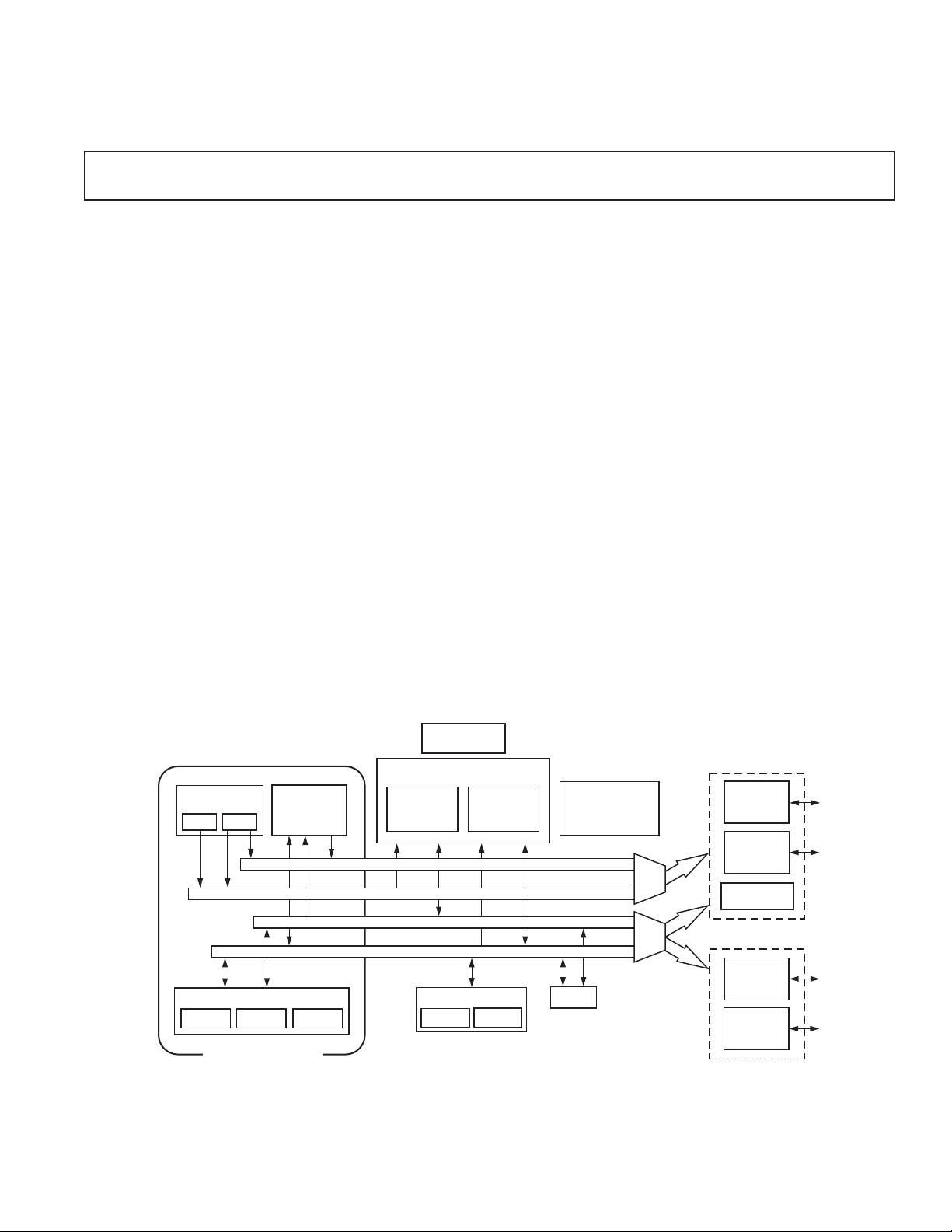
FUNCTIONAL BLOCK DIAGRAM
POWER -DOWN
CONTROL
MEMORY
DATA ADDRESS
GENERATORS
DAG2
DAG1
ARITHMETIC UNITS
ALU
ADSP-2100 BASE
ARCHITECTURE
MAC
PROGRAM
SEQUENCER
SHIFTER
PROGRAM MEMORY ADDRESS
DATA MEMORY ADDRESS
PROGRAM MEMORY DATA
DATA MEMORY DATA
PROGRAM
MEMORY
16K 24 BIT
SERIAL PORTS
SPORT0
REV. 0
Information furnished by Analog Devices is believed to be accurate and
reliable. However, no responsibility is assumed by Analog Devices for its
use, nor for any infringements of patents or other rights of third parties that
may result from its use. No license is granted by implication or otherwise
under any patent or patent rights of Analog Devices.
FULL MEMORY MODE
DATA
MEMORY
16K 16 BIT
SPORT1
One Technology Way, P.O. Box 9106, Norwood, MA 02062-9106, U.S.A.
Tel: 781/329-4700www.analog.com
Fax: 781/326-8703 © Analog Devices, Inc., 2002
PROGRAMMABLE
I/O
AND
FLAGS
TIMER
EXTERNAL
ADDRESS
BUS
EXTERNAL
DATABUS
BYTE DMA
CONTROLLER
OR
EXTERNAL
DATABUS
INTERNAL
DMA
PORT
HOST MODE
Page 2

SST-Melody-DAP
Mute Play (Voice)
Resume Play (Voice)
Download Voice to Flash
Forward to Next Record
Rewind to Previous Record
Delete a Record
Erase Voice Flash
Version Reporting (G.723.1)
Get G.723.1 Record Information
Rename Voice File
Format Flash
Volume Control
Get Song Name
Get Album Name
Get Singer Name
Get Song Duration
Version Reporting
Supports PC Interface
USB 1.1 Interface
Parallel Port Interface
Other Features:
ID3 Tag Support
SDMI Capable
PERFORMANCE
13.3 ns Instruction Cycle Time @ 2.5 V (Internal)
75 MIPS Sustained Performance
Single-Cycle Instruction Execution
Single-Cycle Context Switch
3-Bus Architecture Allows Dual Operand Fetches in
Every Instruction Cycle
Multifunction Instructions
Power-Down Mode Featuring Low CMOS Standby Power
Dissipation with 200 CLKIN Cycle Recovery from
Power-Down Condition
Low Power Dissipation in Idle Mode
INTEGRATION
ADSP-2100 Family Code Compatible (Easy to Use
Algebraic Syntax), with Instruction Set Extensions
80 Kbytes of On-Chip RAM, Configured as 16K Words
Program Memory RAM
16K Words Data Memory RAM
Dual-Purpose Program Memory for Both Instruction and
Data Storage
Independent ALU, Multiplier/Accumulator, and Barrel
Shifter Computational Units
SYSTEM INTERFACE
Flexible I/O Structure Allows 2.5 V or 3.3 V Operation;
All Inputs Tolerate up to 3.6 V Regardless of Mode
16-Bit Internal DMA Port for High Speed Access to
On-Chip Memory (Mode Selectable)
4 MByte Memory Interface for Storage of Data Tables
and Program Overlays (Mode Selectable)
8-Bit DMA to Byte Memory for Transparent Program
and Data Memory Transfers (Mode Selectable)
I/O Memory Interface with 2048 Locations Supports
Parallel Peripherals (Mode Selectable)
Programmable Memory Strobe and Separate I/O
Memory Space Permits “Glueless” System Design
Programmable Wait State Generation
Two Double-Buffered Serial Ports with Companding
Hardware and Automatic Data Buffering
Automatic Booting of On-Chip Program Memory from
Byte-Wide External Memory, e.g., EPROM, or
through Internal DMA Port
Six External Interrupts
13 Programmable Flag Pins Provide Flexible System
Signaling
UART Emulation through Software SPORT
Reconfiguration
ICE-Port™ Emulator Interface Supports Debugging in
Final Systems
ICE-Port is a trademark of Analog Devices, Inc.
REV. 0–2–
Page 3

TABLE OF CONTENTS
SST-Melody-DAP
FEATURES . . . . . . . . . . . . . . . . . . . . . . . . . . . . . . . . . . . . . 1
FUNCTIONAL BLOCK DIAGRAM . . . . . . . . . . . . . . . . . 1
GENERAL DESCRIPTION . . . . . . . . . . . . . . . . . . . . . . . . . 4
SPECIFICATIONS . . . . . . . . . . . . . . . . . . . . . . . . . . . . . . . 4
Instruction Set Description . . . . . . . . . . . . . . . . . . . . . . . . 4
RECOMMENDED OPERATING CONDITIONS . . . . . . . 4
ELECTRICAL CHARACTERISTICS . . . . . . . . . . . . . . . . . 5
ABSOLUTE MAXIMUM RATINGS . . . . . . . . . . . . . . . . . 6
ORDERING INFORMATION . . . . . . . . . . . . . . . . . . . . . . 6
100-LEAD LQFP PIN CONFIGURATION . . . . . . . . . . . . 6
PIN FUNCTION DESCRIPTIONS . . . . . . . . . . . . . . . . . . 7
TIMING SPECIFICATIONS . . . . . . . . . . . . . . . . . . . . . . . 7
GENERAL NOTES . . . . . . . . . . . . . . . . . . . . . . . . . . . . . . . 7
TIMING NOTES . . . . . . . . . . . . . . . . . . . . . . . . . . . . . . . . . 7
MEMORY TIMING SPECIFICATIONS . . . . . . . . . . . . . . 8
FREQUENCY DEPENDENCY FOR
TIMING SPECIFICATIONS . . . . . . . . . . . . . . . . . . . . . . . 8
POWER DISSIPATION . . . . . . . . . . . . . . . . . . . . . . . . . . . . 8
Output Drive Currents . . . . . . . . . . . . . . . . . . . . . . . . . . . . 8
Capacitive Loading . . . . . . . . . . . . . . . . . . . . . . . . . . . . . . 9
SOFTWARE ARCHITECTURE . . . . . . . . . . . . . . . . . . . . 10
ARCHITECTURE OVERVIEW . . . . . . . . . . . . . . . . . . . . 10
Serial Ports . . . . . . . . . . . . . . . . . . . . . . . . . . . . . . . . . . . . 11
PIN DESCRIPTIONS . . . . . . . . . . . . . . . . . . . . . . . . . . . . 11
Common-Mode Pins . . . . . . . . . . . . . . . . . . . . . . . . . . . . 12
Memory Interface Pins . . . . . . . . . . . . . . . . . . . . . . . . . . . 13
Full Memory Mode Pins (Mode C = 0) . . . . . . . . . . . . . . 13
Host Mode Pins (Mode C = 1) . . . . . . . . . . . . . . . . . . . . 13
Interrupts . . . . . . . . . . . . . . . . . . . . . . . . . . . . . . . . . . . . . 15
LOW POWER OPERATION . . . . . . . . . . . . . . . . . . . . . . . 15
Power-Down . . . . . . . . . . . . . . . . . . . . . . . . . . . . . . . . . . 15
Idle . . . . . . . . . . . . . . . . . . . . . . . . . . . . . . . . . . . . . . . . . . 15
Slow Idle . . . . . . . . . . . . . . . . . . . . . . . . . . . . . . . . . . . . . 15
SYSTEM INTERFACE . . . . . . . . . . . . . . . . . . . . . . . . . . . 16
Clock Signals . . . . . . . . . . . . . . . . . . . . . . . . . . . . . . . . . . 16
RESET . . . . . . . . . . . . . . . . . . . . . . . . . . . . . . . . . . . . . . 17
Power Supplies . . . . . . . . . . . . . . . . . . . . . . . . . . . . . . . . . 17
MODES OF OPERATION . . . . . . . . . . . . . . . . . . . . . . . . 17
Setting Memory Mode . . . . . . . . . . . . . . . . . . . . . . . . . . . 17
Passive Configuration . . . . . . . . . . . . . . . . . . . . . . . . . . . . 17
Active Configuration . . . . . . . . . . . . . . . . . . . . . . . . . . . . 18
IACK Configuration . . . . . . . . . . . . . . . . . . . . . . . . . . . . 19
MEMORY ARCHITECTURE . . . . . . . . . . . . . . . . . . . . . . 19
Program Memory . . . . . . . . . . . . . . . . . . . . . . . . . . . . . . . 19
Data Memory . . . . . . . . . . . . . . . . . . . . . . . . . . . . . . . . . . 19
Memory Mapped Registers (New to the
SST-Melody-DAP) . . . . . . . . . . . . . . . . . . . . . . . . . . . . . 20
I/O Space (Full Memory Mode) . . . . . . . . . . . . . . . . . . . . 20
Composite Memory Select (CMS) . . . . . . . . . . . . . . . . . . 20
Byte Memory Select (BMS) . . . . . . . . . . . . . . . . . . . . . . . 20
Byte Memory . . . . . . . . . . . . . . . . . . . . . . . . . . . . . . . . . . 20
Byte Memory DMA (BDMA, Full Memory Mode) . . . . . 20
Internal Memory DMA Port (IDMA Port; Host Memory
Mode) . . . . . . . . . . . . . . . . . . . . . . . . . . . . . . . . . . . . . . . 21
Bootstrap Loading (Booting) . . . . . . . . . . . . . . . . . . . . . . 22
IDMA Port Booting . . . . . . . . . . . . . . . . . . . . . . . . . . . . . 22
Bus Request and Bus Grant . . . . . . . . . . . . . . . . . . . . . . . 22
Flag I/O Pins . . . . . . . . . . . . . . . . . . . . . . . . . . . . . . . . . . 22
OUTLINE DIMENSIONS
100-Lead Metric Thin Plastic Quad Flatpack
(LQFP) (ST-100) . . . . . . . . . . . . . . . . . . . . . . . . . . . . . . 23
Tables
Table I. Memory Timing Specifications . . . . . . . . . . . . . . . . 8
Table II. Environmental Conditions . . . . . . . . . . . . . . . . . . . 8
Table III. Power Dissipation Example . . . . . . . . . . . . . . . . . . 8
Table IV. Pin Terminations . . . . . . . . . . . . . . . . . . . . . . . . . 13
Table V. Interrupt Priority and Interrupt Vector Addresses . 15
Table VI. Modes of Operation . . . . . . . . . . . . . . . . . . . . . . . 17
Table VII. PMOVLAY Bits . . . . . . . . . . . . . . . . . . . . . . . . . 18
Table VIII. DMOVLAY Bits . . . . . . . . . . . . . . . . . . . . . . . . 19
Table IX. Wait States . . . . . . . . . . . . . . . . . . . . . . . . . . . . . 20
Table X. Data Formats . . . . . . . . . . . . . . . . . . . . . . . . . . . . 21
REV. 0
–3–
Page 4

SST-Melody-DAP
GENERAL DESCRIPTION
The SST-Melody-DAP is a single-chip microcomputer optimized for digital signal processing (DSP) and other high speed
numeric processing applications.
The SST-Melody-DAP combines the ADSP-2100 family base
architecture (three computational units, data address generators, and a program sequencer) with two serial ports, a 16-bit
internal DMA port, a byte DMA port, a programmable timer,
flag I/O, extensive interrupt capabilities, and on-chip program
and data memory.
The SST-Melody-DAP integrates 80 Kbytes of on-chip
memory configured as 16K words (24-bit) of program RAM,
and 16K words (16-bit) of data RAM. Power-down circuitry is
also provided to meet the low power needs of battery-operated
portable equipment. The SST-Melody-DAP is available in a
100-lead LQFP package and 144-ball mini-BGA.
In addition, the SST-Melody-DAP supports new instructions, which include bit manipulations—bit set, bit clear, bit
toggle, bit test—new ALU constants, new multiplication
instruction (x squared), biased rounding, result-free ALU
operations, I/O memory transfers, and global interrupt masking, for increased flexibility. Fabricated in a high speed, low
power, CMOS process, the SST-Melody-DAP operates with a
13.3 ns instruction cycle time. Every instruction can execute in
a single processor cycle.
The SST-Melody-DAP’s flexible architecture and comprehensive instruction set allow the processor to perform multiple
operations in parallel. In one processor cycle, the SST-MelodyDAP can:
• Generate the next program address
• Fetch the next instruction
• Perform one or two data moves
• Update one or two data address pointers
• Perform a computational operation
This takes place while the processor continues to:
• Receive and transmit data through the two serial ports
• Receive and/or transmit data through the internal DMA port
• Receive and/or transmit data through the byte DMA port
• Decrement timer
Instruction Set Description
The SST-Melody-DAP assembly language instruction set has
an algebraic syntax that was designed for ease of coding and
readability.
The assembly language, which takes full advantage of the
processor’s unique architecture, offers the following benefits:
• The algebraic syntax eliminates the need to remember cryptic
assembler mnemonics. For example, a typical arithmetic add
instruction, such as AR = AX0 + AY0, resembles a simple
equation.
• Every instruction assembles into a single, 24-bit word that
can execute in a single instruction cycle.
• The syntax is a superset ADSP-2100 family assembly language and is completely source and object code compatible
with other family members. Programs may need to be relocated to utilize on-chip memory and conform to the
SST-Melody-DAP’s interrupt vector and reset vector map.
• Sixteen condition codes are available. For conditional
jump, call, return, or arithmetic instructions, the condition
can be checked and the operation executed in the same
instruction cycle.
• Multifunction instructions allow parallel execution of an
arithmetic instruction with up to two fetches or one write to
processor memory space during a single instruction cycle.
SPECIFICATIONS
RECOMMENDED OPERATING CONDITIONS
K Grade B Grade
Parameter Min Max Min Max Unit
V
DDINT
V
DDEXT
V
INPUT
T
AMB
Specifications subject to change without notice.
2.37 2.63 2.25 2.75 V
2.37 3.6 2.25 3.6 V
VIL = –0.3 VIH = +3.6 VIL = –0.3 VIH = +3.6 V
0 +70 –40 +85 °C
REV. 0–4–
Page 5

SST-Melody-DAP
ELECTRICAL CHARACTERISTICS
K/B Grades
Parameter Test Conditions Min Typ Max Unit
V
Hi-Level Input Voltage
IH
VIHHi-Level CLKIN Voltage @ V
VILLo-Level Input Voltage
VOHHi-Level Output Voltage
VOLLo-Level Output Voltage
I
Hi-Level Input Current
IH
I
Lo-Level Input Current
IL
I
Three-State Leakage Current7@ V
OZH
I
Three-State Leakage Current7@ V
OZL
I
Supply Current (Idle)
DD
I
Supply Current (Dynamic)
DD
I
Supply Current (Power-Down)11@ V
DD
C
Input Pin Capacitance
I
COOutput Pin Capacitance
NOTES
1
Bidirectional pins: D0–D3, RFS0, RFS1, SCLK0, SCLK1, TFS0, TFS1, A1–A13, PF0–PF7
2
Input only pins: RESET, BR, DR0, DR1, PWD.
3
Input only pins: CLKIN, RESET, BR, DR0, DR1, PWD
4
Output pins: BG, PMS, DMS, BMS, IOMS, CMS, RD, WR, PWDACK, A0, DT0, DT1, CLKOUT, FL2–0, BGH
5
Although specified for TTL outputs, all ADSP-2185M outputs are CMOS compatible and will drive to V
6
Guaranteed but not tested
7
Three-statable pins: A0–A13, D0–D23, PMS, DMS, BMS, IOMS, CMS, RD, WR, DT0, DT1, SCLK0, SCLK1, TFS0, TFS1, RFS0, RFS1, PF0–PF7
8
0 V on BR
9
IDD measurement taken with all instructions executing from internal memory. 50% of the instructions are multifunctional (types 1, 4, 5, 12, 13, 14), 30% are type 2
and type 6, and 20% are idle instructions.
10
VIN = 0 V and 3 V. For typical figures for supply currents, refer to Power Dissipation section.
11
See Chapter 9 of the ADSP-2100 Family User’s Manual (3rd Edition, 9/95) for details.
12
Output pin capacitance is the capacitive load for any three-stated output pin.
Specifications subject to change without notice.
1, 2
1, 3
1, 4, 5
1, 4, 5
3
3
9
3, 6
6, 7, 11, 12
@ V
@ V
@ V
@ V
@ V
@ V
@ V
@ V
@ V
@ V
9
@ V
@ V
= max
DDINT
= max
DDINT
= min
DDINT
= min, IOH = –0.5 mA
DDEXT
= 3.0 V, IOH = –0.5 mA
DDEXT
= min, IOH = –100 mA
DDEXT
= min, IOL = 2 mA
DDEXT
= max, VIN = 3.6 V 10
DDINT
= max, VIN = 0 V 10
DDINT
= max, VIN = 3.6 V
DDEXT
= max, VIN = 0 V
DDEXT
= 2.5, t
DDINT
= 2.5, t
DDINT
= 2.5, 15 ns10, T
DDINT
= 2.5, 13.3 ns10, T
DDINT
= 2.5, T
DDINT
Power Mode
@ VIN = 2.5 V, fIN = 1.0 MHz, T
@ VIN = 2.5 V, fIN = 1.0 MHz, T
8
8
= 15 ns
CK
= 13.3 ns
CK
AMB
AMB
= 25°C in Lowest
AMB
1.5 V
2.0 V
0.7 V
2.0 V
2.4 V
6
V
– 0.3 V
DDEXT
0.4 V
A
A
10
10
A
A
9mA
10 mA
= 25°C
= 25°C
35 mA
38 mA
100 A
= 25°C8pF
AMB
= 25°C8pF
AMB
and GND, assuming no dc loads.
DDEXT
REV. 0
–5–
Page 6
SST-Melody-DAP
WARNING!
ESD SENSITIVE DEVICE
ABSOLUTE MAXIMUM RATINGS
Internal Supply Voltage (V
Internal Supply Voltage (V
Input Voltage
2
. . . . . . . . . . . . . . . . . . . . . . . . –0.5 V to +4.0 V
Output Voltage Swing
DDINT
DDEXT
3
. . . . . . . . . . –0.5 V to V
1
) . . . . . . . . . –0.3 V to +3.0 V
) . . . . . . . . . –0.3 V to +4.0 V
+ 0.5 V
DDEXT
Operating Temperature Range . . . . . . . . . . . –40°C to +85°C
Storage Temperature Range . . . . . . . . . . . . –65°C to +150°C
Lead Temperature (5 sec) LQFP . . . . . . . . . . . . . . . . . . 280°C
NOTES
1
Stresses above those listed under Absolute Maximum Ratings may cause
permanent damage to the device. This is a stress rating only and functional
operation of the device at these or any other conditions above those listed in the
operational sections of this specification is not implied. Exposure to absolute
maximum rating conditions for extended periods may affect device reliability.
2
Applies to bidirectional pins (D0–D3, RFS0, RFS1, SCLK0, SCLK1, TFS0,
TFS1, A1–A13, PF0–PF7) and input only pins (CLKIN, RESET, BR, DR0,
DR1, PWD)
3
Applies to output pins (BG, PMS, DMS, BMS, IOMS, CMS, RD, WR,
PWDACK, A0, DT0, DT1, CLKOUT, FL2–0, BGH)
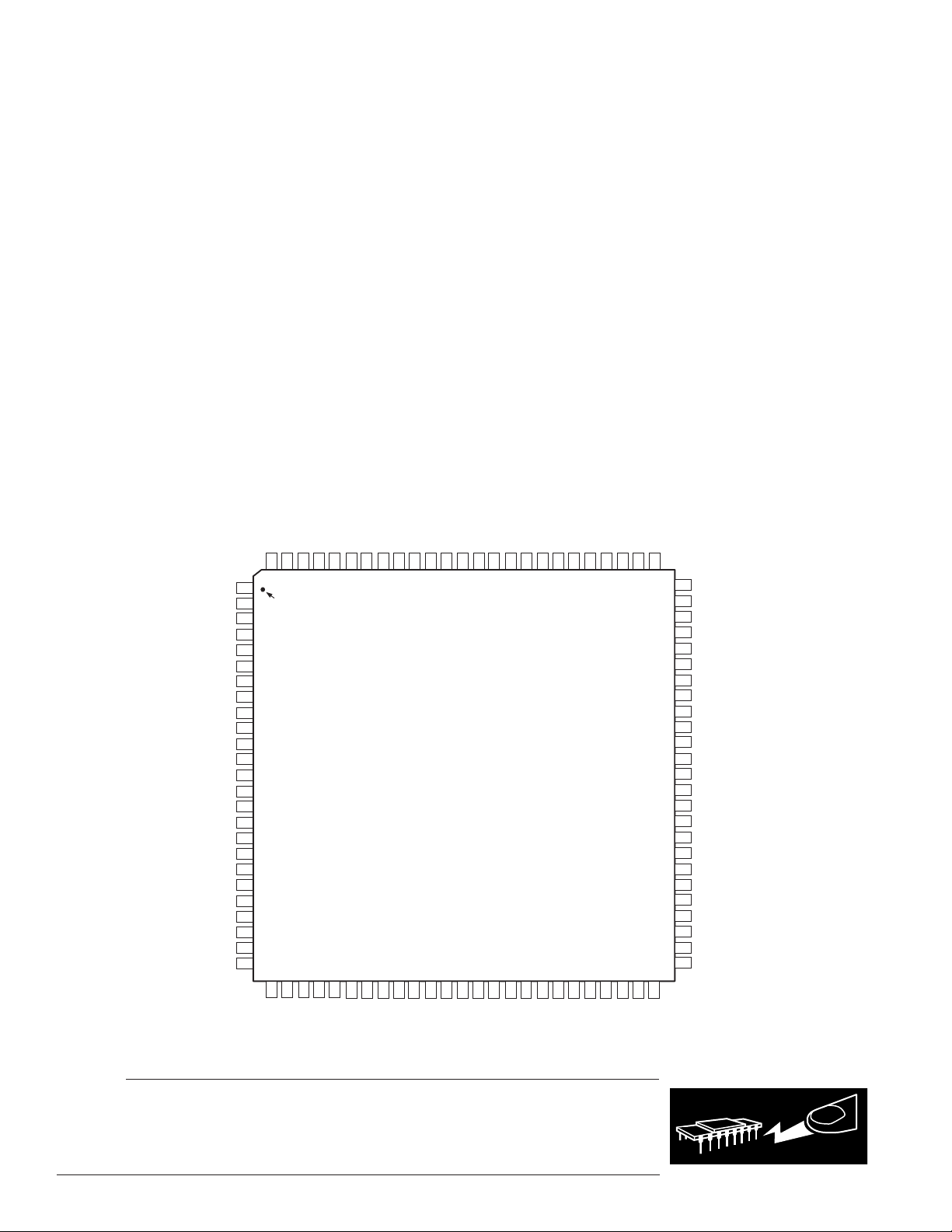
100-LEAD LQFP
PIN CONFIGURATION
DDEXT
V
GND
PWD
PF2 [MODE C]
929190
89
SST-Melody-DAP
TOP VIEW
(Not to Scale)
SCLK0
DDEXT
V
37
DT1/FO
343536
DR0
A4/IAD3
A5/IAD4
GND
A6/IAD5
A7/IAD6
A8/IAD7
A9/IAD8
A10/IAD9
A11/IAD10
A12/IAD11
A13/IAD12
GND
CLKIN
XTAL
V
DDEXT
CLKOUT
GND
V
DDINT
WR
BMS
DMS
PMS
IOMS
CMS
RD
A3/IAD2
A2/IAD1
A1/IAD0A0PWDACK
99989796959493
100
1
PIN 1
2
IDENTIFIER
3
4
5
6
7
8
9
10
11
12
13
14
15
16
17
18
19
20
21
22
23
24
25
262827
GND
IRQE+PF4
IRQL0+PF5
29
IRQL1+PF6
30
IRQ2+PF7
BGH
PF0 [MODE A]
PF1 [MODE B]
31
33
32
DT0
TFS0
RFS0
ORDERING INFORMATION
The Analog Devices SST-Melody-DAP Reference Design
must be ordered under the part number ADSST-MelodySDK for the
standalone reference design. This includes the
evaluation board with an evaluation copy of the software and
schematics.
Designers of products using this reference design also will be
required to sign a license agreement with the respective license
holder––
i.e., Digital Theater Systems (DTS), Dolby Laboratories, THX Ltd., Microsoft, or SRS Labs––to use the
appropriate code and produce proof to Analog Devices of
having successfully completed the appropriate licensing procedures before final products can be
shipped to them. The final
product will be shipped from Analog Devices and will include
the decoder chipset and software; customers will be required to
sign license agreements with Analog Devices and separately pay
system royalties to the respective license holder.
PF3 [MODE D]
FL0
FL1
FL2
D23
D22
D21
D20
GND
D19
D18
D17
8786858483
88
39
40
38
DR1/FI
TFS1/IRQ1
RFS1/IRQ0
414243
GND
SCLK1
81
82
4445464748
EMS
RESET
ERESET
79
80
EE
ECLK
78
77
49
ELIN
ELOUT
D16
76
50
EINT
75
74
73
72
71
70
69
68
67
66
65
64
63
62
61
60
59
58
57
56
55
54
53
52
51
D15
D14
D13
D12
GND
D11
D10
D9
V
DDEXT
GND
D8
D7/IWR
D6/IRD
D5/IAL
D4/IS
GND
V
DDINT
D3/IACK
D2/IAD15
D1/IAD14
D0/IAD13
BG
EBG
BR
EBR
CAUTION
ESD (electrostatic discharge) sensitive device. Electrostatic charges as high as 4000 V readily
accumulate on the human body and test equipment and can discharge without detection. Although
SST-Melody-DAP
the
features proprietary ESD protection circuitry, permanent damage may
occur on devices subjected to high energy electrostatic discharges. Therefore, proper ESD
precautions are recommended to avoid performance degradation or loss of functionality.
REV. 0–6–
Page 7

SST-Melody-DAP
The LQFP package pinout is shown in the Pin Function Descriptions. Pin names in bold text replace the plain text named functions
when Mode C = 1. A plus (+) sign separates two functions when either function can be active for either major I/O mode. Signals
enclosed in brackets [ ] are state bits latched from the value of the pin at the deassertion of RESET.
The multiplexed pins DT1/FO, TFS1/IRQ1, RFS1/IRQ0, and DR1/FI are mode selectable by setting Bit 10 (SPORT1 configure) of
the System Control register. If Bit 10 = 1, these pins have serial port functionality. If Bit 10 = 0, these pins are the external interrupt
and flag pins. This bit is set to 1 by default upon reset.
PIN FUNCTION DESCRIPTION
Pin
No. Mnemonic
1 A4/IAD3
2 A5/IAD4
3GND
4 A6/IAD5
5 A7/IAD6
6 A8/IAD7
7 A9/IAD8
8 A10/IAD9
9 A11/IAD10
10 A12/IAD11
11 A13/IAD12
12 GND
13 CLKIN
14 XTAL
15 V
DDEXT
16 CLKOUT
17 GND
18 V
DDINT
19 WR
20 RD
21 BMS
22 DMS
23 PMS
24 IOMS
25 CMS
Pin
No. Mnemonic
26 IRQE+PF4
27 IRQL0+PF5
28 GND
29 IRQL1+PF6
30 IRQ2+PF7
31 DT0
32 TFS0
33 RFS0
34 DR0
35 SCLK0
36 V
DDEXT
37 DT1/FO
38 TFS1/IRQ1
39 RFS1/IRQ0
40 DR1/FI
41 GND
42 SCLK1
43 ERESET
44 RESET
45 EMS
46 EE
47 ECLK
48 ELOUT
49 ELIN
50 EINT
Pin
No. Mnemonic
51 EBR
52 BR
53 EBG
54 BG
55 D0/IAD13
56 D1/IAD14
57 D2/IAD15
58 D3/IACK
59 V
DDINT
60 GND
61 D4/IS
62 D5/IAL
63 D6/IRD
64 D7/IWR
65 D8
66 GND
67 V
DDEXT
68 D9
69 D10
70 D11
71 GND
72 D12
73 D13
74 D14
75 D15
Pin
No. Mnemonic
76 D16
77 D17
78 D18
79 D19
80 GND
81 D20
82 D21
83 D22
84 D23
85 FL2
86 FL1
87 FL0
88 PF3 [MODE D]
89 PF2 [MODE C]
90 V
DDEXT
91 PWD
92 GND
93 PF1 [MODE B]
94 PF0 [MODE A]
95 BGH
96 PWDACK
97 A0
98 A1/IAD0
99 A2/IAD1
100 A3/IAD2
TIMING SPECIFICATIONS
GENERAL NOTES
Use the exact timing information given. Do not attempt to
derive parameters from the addition or subtraction of others.
While addition or subtraction would yield meaningful results for
an individual device, the values given in this data sheet reflect
statistical variations and worst cases. Consequently, the user
cannot meaningfully add up parameters to derive longer times.
TIMING NOTES
Switching characteristics specify how the processor changes its
signals. There is no control over this. Timing circuitry external
to the processor must be designed for compatibility with these
REV. 0
–7–
signal characteristics. Switching characteristics tell what the
processor will do in a given circumstance. Switching characteristics may be used to ensure that any timing requirement of a
device connected to the processor (such as memory) is satisfied.
Timing requirements apply to signals that are controlled by
circuitry external to the processor, such as the data input for a
read operation. Timing requirements guarantee that the processor operates correctly with other devices.
MEMORY TIMING SPECIFICATIONS
Table I shows common memory device specifications and the
corresponding SST-Melody-DAP timing parameters, for your
convenience.
Page 8
SST-Melody-DAP
Table I. Memory Timing Specifications
Memory Timing
Device Parameter
Specification Parameter Definition*
Address Setup to t
ASW
A0–A13, xMS Setup
Write Start before WR Low
Address Setup to t
AW
A0–A13, xMS Setup
Write End before WR Deasserted
Address Hold t
WRA
A0–A13, xMS Hold
Time before WR Low
Data Setup Time
Data Hold Time
OE to Data Valid
Address Access t
t
DW
t
DH
t
RDD
AA
Data Setup before WR High
Data Hold after WR High
RD Low to Data Valid
A0–A13, xMS to
Time Data Valid
*xMS = PMS, DMS, CMS, or IOMS.
FREQUENCY DEPENDENCY FOR TIMING SPECIFICATIONS
tCK is defined as 0.5 t
. The SST-Melody-DAP uses an input
CKI
clock with a frequency equal to half the instruction rate. For
example, a 37.50 MHz input clock (which is equivalent to 26.6 ns)
yields a 13.3 ns processor cycle (equivalent to 75 MHz). t
values within the range of 0.5 t
period should be substituted
CKI
CK
for all relevant timing parameters to obtain the specification value.
Example: t
= 0.5 tCK – 2 ns = 0.5 (15 ns) – 2 ns = 5.5 ns
CKH
Table II. Environmental Conditions*
Rating
Description Symbol LQFP Mini-BGA
Thermal Resistance
CA
48°C/W 63.3°C/W
(Case-to-Ambient)
Thermal Resistance
JA
50°C/W 70.7°C/W
(Junction-to-Ambient)
Thermal Resistance
JC
2°C/W 7.4°C/W
(Junction-to-Case)
*Where the Ambient Temperature Rating (T
T
= T
AMB
T
CASE
PD = Power Dissipation in W
– (PD ⫻ CA)
CASE
= Case Temperature in °C
AMB
) is:
POWER DISSIPATION
To determine total power dissipation in a specific application,
the following equation should be applied for each output:
CV f
2
××
DD
C = load capacitance, f = output switching frequency.
Example:
In an application where external data memory is used and no
other outputs are active, power dissipation is calculated as follows:
Assumptions:
•
External data memory is accessed every cycle with 50% of the
address pins switching.
•
External data memory writes occur every other cycle with
50% of the data pins switching.
•
Each address and data pin has a 10 pF total load at the pin.
The application operates at V
•
= 30 ns.
t
CK
Total Power Dissipation = P
P
= internal power dissipation from Power vs. Frequency
INT
+ (C ⫻ V
INT
DDEXT
= 3.3 V and
2
⫻ f)
DDEXT
graph (see Figures 2a through 2c).
(C ⫻ V
2
⫻ f) is calculated for each output:
DDEXT
Table III. Power Dissipation Example
No. of C
V
Parameter Pins (pF) (V) (MHz)
Address 7 10 3.3
Data Output, WR
RD
CLKOUT, DMS
910
1
10
3.3
3.3
2103.3
DDEXT
2
2
2
2
2
f
16.67 12.7
16.67 16.6
16.67 1.8
33.3 7.2
PD
(mW)
Total 38.2
Total power dissipation for this example is P
+ 38.0 mW.
INT
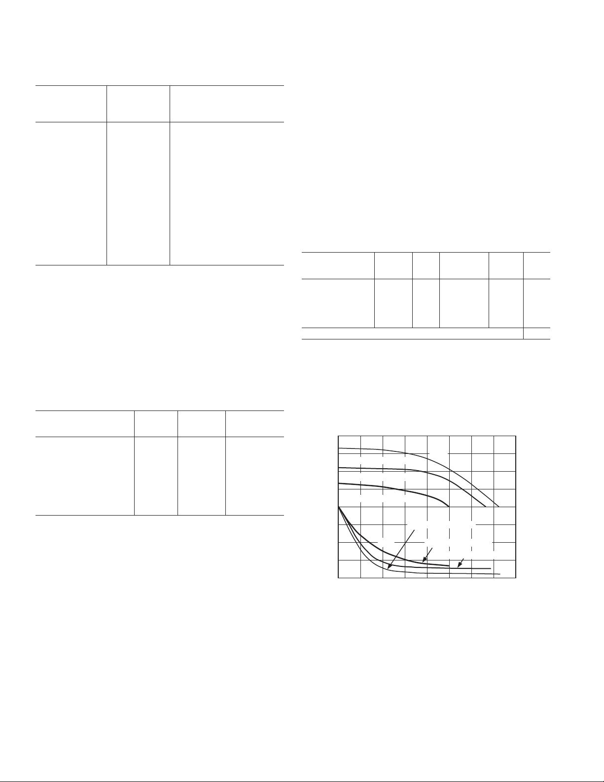
Output Drive Currents
Figure 1 shows typical I–V characteristics for the output
drivers
on the SST-Melody-DAP. The curves represent the
current drive
capability of the output drivers as a function of
output voltage.
80
V
DDEXT
V
VOH
– 3.6V @ –40C
– 2.5V @ +85C
DDEXT
V
– 3.3V @ +25C
DDEXT
60
V
– 3.6V @ –40C
DDEXT
40
V
– 3.3V @ +25C
DDEXT
20
V
– 2.5V @ +85C
DDEXT
0
–20
SOURCE CURRENT – mA
–40
–60
–80
0
VOL
0.5 1.0 1.5 2.0 2.5 3.0 3.5 4.0
SOURCE VOLTAGE – V
Figure 1. Typical Output Driver Characteristics
REV. 0–8–
Page 9

SST-Melody-DAP
CL – pF
0
RISE TIME (0.4V–2.4V) – ns
50 100
0
150
200 250 300
15
20
25
30
10
5
T = 85C
V
DD
= 0V TO 2.0V
CL – pF
0
VA LID OUTPUT DELAY OR HOLD – ns
50 100
–6
150 200 250
6
10
14
18
2
–2
4
8
12
16
NOMINAL
–4
115
110
105
100
95
90
) – mW
INT
85
80
75
POWER (P
70
65
60
55
30
28
26
24
) – mW
IDLE
22
20
POWER (P
18
16
50
82mW
70mW
61mW
24mW
20mW
16.5mW
POWER, INTERNAL
VDD – 2.65V
VDD – 2.5V
VDD – 2.35V
55 60
1/tCK – MHz
POWER, IDLE
VDD – 2.65V
VDD – 2.5V
VDD – 2.35V
1, 2, 3
110mW
Capacitive Loading
Figures 3 and 4 show the capacitive loading characteristics of
the SST-Melody-DAP.
95mW
82mW
65
70 75 80
1, 2, 4
28mW
Figure 3. Typical Output Rise Time vs. Load Capacitance
(at Maximum Ambient Operating Temperature)
24mW
20mW
REV. 0
14
50
26
24
22
) – mW
n
20
IDLE
18
POWER (P
16
14
12
50
NOTES
VA LID FOR ALL TEMPERATURE GRADES.
1
POWER REFLECTS DEVICE OPERATING WITH NO OUTPUT LOADS.
2
TYPICAL POWER DISSIPATION AT 2.5V V
WHERE SPECIFIED.
3
IDO MEASUREMENT TAKEN WITH ALL INSTRUCTIONS EXECUTING
FROM INTERNAL MEMORY. 50% OF THE INSTRUCTIONS ARE
MULTIFUNCTION (TYPES 1, 4, 5, 12, 13, 14), 20% ARE TYPE 2 AND TYPE 6,
AND 20% ARE IDLE INSTRUCTIONS.
4
IDLE REFERS TO STATE OF OPERATING DURING EXECUTION OF IDLE
INSTRUCTION. DEASSERTED PINS ARE DRIVEN TO EITHER V
20mW
15mW
14.25mW
55 60
65
1/tCK – MHz
POWER, IDLE nMODES
55 60
65
1/tCK – MHz
70 75 80
2
24mW
16.4mW
15.7mW
70 75 80
AND 25C, EXCEPT
DIDINT
Figure 2. Power vs. Frequency
OR GND.
DD
IDLE
IDLE (16)
IDLE (128)
–9–
Figure 4. Typical Output Valid Delay or Hold vs.
Load Capacitance, C
(at Maximum Ambient
L
Operating Temperature)
Page 10

SST-Melody-DAP
SOFTWARE ARCHITECTURE
The SST-Melody-DAP software programming model has
the following parts:
•
Executive kernel
•
Algorithm suite as library modules
The executive kernel has the following functions:
•
Power-up hardware initialization
•
Serial port management
•
Automatic stream detect
•
Automatic code load
•
Command processing
•
Interrupt handling
•
Data buffer management
EXECUTIVE KERNEL
INPUT STREAM OUTPUT STREAM
DECODING LIBRARY
•
Calling library module
•
Status report
The executive kernel is executed as soon as booting takes place.
The hardware resources are initialized in the beginning. The
“command buffer” and general-purpose programmable flag pins
are initialized. Various data buffers and memory variables are
initialized. Interrupts are programmed and enabled. Then definite signatures are written “command buffer” to inform the host
that ADSP is ready to receive the commands. Once commands
are issued by host micro, these are executed and appropriate
action takes place. Decoding is handled by issuing appropriate
commands by host micro.
The kernel communicates with the library module for a particular algorithm in a definite way. The details are found in the
specific implementation documents.
ARCHITECTURE OVERVIEW
The SST-Melody-DAP instruction set provides flexible data
moves and multifunction (one or two data moves with a computation) instructions. Every instruction can be executed in a
single processor cycle. The SST-Melody-DAP assembly language
uses an algebraic syntax for ease of coding and readability. A
comprehensive set of development tools supports program
development.
A functional block diagram of the SST-Melody-DAP is provided. The processor contains three independent computational
units: the ALU, the multiplier/accumulator (MAC), and the
shifter. The computational units process 16-bit data directly
and have provisions to support multiprecision computations.
The ALU performs a standard set of arithmetic and logic operations; division primitives are also supported. The MAC performs
single-cycle multiply, multiply/add, and multiply/subtract operations with 40 bits of accumulation. The shifter performs logical
and arithmetic shifts, normalization, denormalization, and derive exponent operations.
The shifter can be used to efficiently implement numeric
format control, including multiword and block floating-point
representations.
The internal result (R) bus connects the computational units so
that the output of any unit may be the input of any unit on the
next cycle.
A powerful program sequencer and two dedicated data address
generators ensure efficient delivery of operands to these computational units. The sequencer supports conditional jumps,
subroutine calls, and returns in a single cycle. With internal
loop counters and loop stacks, the SST-Melody-DAP executes
looped code with zero overhead; no explicit jump instructions
are required to maintain loops.
Two data address generators (DAGs) provide addresses for
simultaneous dual operand fetches (from data memory and
program memory). Each DAG maintains and updates four
address pointers. Whenever the pointer is used to access data
(indirect addressing), it is postmodified by the value of one of
four possible modify registers. A length value may be associated
with each pointer to implement automatic modulo addressing
for circular buffers.
Efficient data transfer is achieved with the use of five
internal buses:
•
Program Memory Address (PMA) Bus
•
Program Memory Data (PMD) Bus
•
Data Memory Address (DMA) Bus
•
Data Memory Data (DMD) Bus
•
Result (R) Bus
REV. 0–10–
Page 11

SST-Melody-DAP
The two address buses (PMA and DMA) share a single external
address bus, allowing memory to be expanded off-chip. The two
databuses (PMD and DMD) share a single external databus.
Byte memory space and I/O memory space also share the
external buses.
Program memory can store both instructions and data, permitting the SST-Melody-DAP to fetch two operands in a single
cycle, one from program memory and one from data memory.
The SST-Melody-DAP can fetch an operand from program
memory and the next instruction in the same cycle. In lieu of
the address and databus for external memory connection, the
SST-Melody-DAP may be configured for 16-bit Internal DMA
port (IDMA port) connection to external systems. The IDMA
port is made up of 16 data/address pins and five control pins.
The IDMA port provides transparent, direct access to the DSP’s
on-chip program and data RAM.
An interface to low cost byte-wide memory is provided by the
Byte DMA port (BDMA port). The BDMA port is bidirectional
and can directly address up to four megabytes of external RAM
or ROM for off-chip storage of program overlays or data tables.
The byte memory and I/O memory space interface supports
slow memories and I/O memory-mapped peripherals with programmable wait state generation. External devices can gain
control of external buses with bus request/grant signals (BR,
BGH, and BG).
One execution mode (Go Mode) allows the SST-Melody-DAP
to continue running from on-chip memory. Normal execution
mode requires the processor to halt while buses are granted.
The SST-Melody-DAP can respond to 11 interrupts. There can
be up to six external interrupts (one edge-sensitive, two levelsensitive, and three configurable) and seven internal interrupts
generated by the timer, the serial ports (SPORTs), the Byte
DMA port, and the power-down circuitry. There is also a master RESET signal. The two serial ports provide a complete
synchronous serial interface with optional companding in hardware and a wide variety of framed or frameless data transmit
and receive modes of operation.
Each port can generate an internal programmable serial clock or
accept an external serial clock.
The SST-Melody-DAP provides up to 13 general-purpose
flag pins. The data input and output pins on SPORT1 can be
alternatively configured as an input flag and an output flag.
In addition, eight flags are programmable as inputs or outputs, and three flags are always outputs.
A programmable interval timer generates periodic interrupts.
A 16-bit count register (TCOUNT) decrements every n processor cycle, where n is a scaling value stored in an 8-bit
register (TSCALE). When the value of the count register reaches
zero, an interrupt is generated and the count register is reloaded
from a 16-bit period register (TPERIOD).
Serial Ports
The SST-Melody-DAP incorporates two complete synchronous
serial ports (SPORT0 and SPORT1) for serial communications
and multiprocessor communication.
Here is a brief list of the capabilities of the SST-Melody-DAP
SPORTs:
•
SPORTs are bidirectional and have a separate, double buffered transmit and receive section.
•
SPORTs can use an external serial clock or generate their
own serial clock internally.
•
SPORTs have independent framing for the receive and transmit sections. Sections run in a frameless mode or with frame
synchronization signals internally or externally generated.
Frame sync signals are active high or inverted, with either of
two pulsewidths and timings.
•
SPORTs support serial data-word lengths from three to 16 bits
and provide optional A-law and µ-law companding
according to CCITT recommendation G.711.
•
SPORT receive and transmit sections can generate unique
interrupts on completing a data-word transfer.
•
SPORTs can receive and transmit an entire circular buffer of
data with only one overhead cycle per data-word. An interrupt is generated after a data buffer transfer.
•
SPORT0 has a multichannel interface to selectively receive
and transmit a 24- or 32-word, time-division multiplexed,
serial bitstream.
•
SPORT1 can be configured to have two external interrupts
(IRQ0 and IRQ1) and the FI and FO signals. The internally
generated serial clock may still be used in this configuration.
PIN DESCRIPTIONS
The SST-Melody-DAP is available in a 100-lead LQFP package
and a 144-ball mini-BGA package. In order to maintain maximum functionality and reduce package size and pin count, some
serial port, programmable flag, interrupt, and external bus pins
have dual multiplexed functionality. The external bus pins are
configured during RESET only, while serial port pins are software configurable during program execution. Flag and interrupt
functionality is retained concurrently on multiplexed pins. In
cases where pin functionality is reconfigurable, the default state
is shown in plain text; alternate functionality is shown in italics.
REV. 0
–11–
Page 12

SST-Melody-DAP
Common-Mode Pins
Mnemonic No. of Pins I/O Function
RESET 1I Processor Reset Input
BR 1I Bus Request Input
BG 1OBus Grant Output
BGH 1OBus Grant Hung Output
DMS 1OData Memory Select Output
PMS 1OProgram Memory Select Output
IOMS 1OMemory Select Output
BMS 1OByte Memory Select Output
CMS 1OCombined Memory Select Output
RD 1OMemory Read Enable Output
WR 1OMemory Write Enable Output
IRQ2 1I Edge- or Level-Sensitive Interrupt Request
PF7 I/O Programmable I/O Pin
IRQL1 1I Level-Sensitive Interrupt Requests
1
PF6 I/O Programmable I/O Pin
IRQL0 1I Level-Sensitive Interrupt Requests
1
PF5 I/O Programmable I/O Pin
IRQE 1I Edge-Sensitive Interrupt Requests
1
PF4 I/O Programmable I/O Pin
Mode D 1 I Mode Select Input—Checked Only During RESET
PF3 I/O Programmable I/O Pin During Normal Operation
Mode C 1 I Mode Select Input—Checked Only During RESET
PF2 I/O Programmable I/O Pin During Normal Operation
Mode B 1 I Mode Select Input—Checked Only During RESET
PF1 I/O Programmable I/O Pin During Normal Operation
Mode A 1 I Mode Select Input—Checked Only During RESET
PF0 I/O Programmable I/O Pin During Normal Operation
CLKIN, XTAL 2 I Clock or Quartz Crystal Input
CLKOUT 1 O Processor Clock Output
SPORT0 5 I/O Serial Port I/O Pins
SPORT1 5 I/O Serial Port I/O Pins
IRQ1:IRQ0, FI, FO Edge- or Level-Sensitive Interrupts, FI, FO
PWD 1I Power-Down Control Input
PWDACK 1 O Power-Down Control Output
FL0, FL1, FL2 3 O Output Flags
V
DDINT
V
DDEXT
2I Internal VDD (2.5 V) Power (LQFP)
4I External VDD (2.5 V or 3.3 V) Power (LQFP)
GND 10 I Ground (LQFP)
V
DDINT
V
DDEXT
4I Internal VDD (2.5 V) Power (Mini-BGA)
7I External VDD (2.5 V or 3.3 V) Power (Mini-BGA)
GND 20 I Ground (Mini-BGA)
EZ-Port 9 I/O For Emulation Use
NOTES
1Interrupt/Flag pins retain both functions concurrently. If IMASK is set to enable the corresponding interrupts, then the DSP will vector to the appropriate interrupt vector
address when the pin is asserted, either by external devices, or set as a programmable flag.
2
SPORT configuration determined by the DSP System Control Register. Software configurable.
1
2
REV. 0–12–
Page 13

SST-Melody-DAP
Memory Interface Pins
The SST-Melody-DAP processor can be used in one of two modes: Full Memory Mode, which allows BDMA operation with full external overlay memory and I/O capability, or Host Mode, which allows IDMA operation with limited external addressing capabilities. The
operating mode is determined by the state of the Mode C Pin during RESET and cannot be changed while the processor is running.
The following tables list the active signals at specific pins of the DSP during either of the two operating modes (Full Memory or
Host). A signal in one table shares a pin with a signal from the other table, with the active signal determined by the mode set. For the
shared pins and their alternate signals (e.g., A4/IAD3), refer to the package pinout tables.
Full Memory Mode Pins (Mode C = 0)
Mnemonic No. of Pins I/O Function
A13:0 14 O
D23:0 24 I/O Data I/O Pins for Program, Data, Byte, and I/O Spaces
Host Mode Pins (Mode C = 1)
Mnemonic No. of Pins I/O Function
IAD15:0 16 I/O IDMA Port Address/Data Bus
A0 1 O Address Pin for External I/O, Program, Data, or
D23:8 16 I/O Data I/O Pins for Program, Data, Byte, and I/O Spaces
IWR 1IIDMA Write Enable
IRD 1IIDMA Read Enable
IAL 1 I IDMA Address Latch Pin
IS 1IIDMA Select
IACK 1O
*In Host Mode, external peripheral addresses can be decoded using the A0, CMS, PMS, DMS, and IOMS signals.
Table IV. Pin Terminations
Table IV shows the recommendations for terminating unused pins.
I/O Three-State Reset Hi-Z
Mnemonic (Z) State Caused By Unused Configuration
XTAL I I Float
CLKOUT O O Float
A13:1 or O (Z) Hi-Z BR, EBR Float
IAD 12:0 I/O (Z) Hi-Z IS Float
A0 O (Z) Hi-Z BR, EBR Float
D23:8 I/O (Z) Hi-Z BR, EBR Float
D7 or I/O (Z) Hi-Z BR, EBR Float
IWR II High (Inactive)
D6 or I/O (Z) Hi-Z BR, EBR Float
IRD IIBR, EBR High (Inactive)
D5 or I/O (Z) Hi-Z Float
IAL I I Low (Inactive)
D4 or I/O (Z) Hi-Z BR, EBR Float
IS II High (Inactive)
D3 or I/O (Z) Hi-Z BR, EBR Float
IACK Float
D2:0 or I/O (Z) Hi-Z BR, EBR Float
IAD15:13 I/O (Z) Hi-Z IS Float
Address Output Pins for Program, Data, Byte, and I/O Spaces
(8 MSBs are also used as Byte Memory Addresses)
Byte Access
IDMA Port Acknowledge Configurable in Mode D; Open Drain
*
1, 2, 3, 4
5
REV. 0
–13–
Page 14

SST-Melody-DAP
Table IV. Pin Terminations (continued)
Mnemonic (Z) State Caused By Unused Configuration
I/O Three-State Reset Hi-Z
PMS O (Z) O BR, EBR Float
DMS O (Z) O BR, EBR Float
BMS O (Z) O BR, EBR Float
IOMS O (Z) O BR, EBR Float
CMS O (Z) O BR, EBR Float
RD O (Z) O BR, EBR Float
WR O (Z) O BR, EBR Float
BR II High (Inactive)
BG O (Z) O EE Float
BGH OO Float
IRQ2/PF7 I/O (Z) I Input = High (Inactive) or
IRQL1/PF6 I/O (Z) I Input = High (Inactive) or
IRQL0/PF5 I/O (Z) I Input = High (Inactive) or
IRQE/PF4 I/O (Z) I Input = High (Inactive) or
SCLK0 I/O I Input = High or Low,
RFS0 I/O I High or Low
DR0 I I High or Low
TFS0 I/O I High or Low
DT0 O O Float
SCLK1 I/O I Input = High or Low,
RFS1/IRQ0 I/O I High or Low
DR1/FI I I High or Low
TFS1/IRQ1 I/O I High or Low
DT1/FO O O Float
EE I I Float
EBR II Float
EBG OO Float
ERESET II Float
EMS OO Float
EINT II Float
ECLK I I Float
ELIN I I Float
ELOUT O O Float
NOTES
1
If the CLKOUT Pin is not used, turn it off using CLKODIS in SPORT0 autobuffer control register.
2
If the interrupt/programmable flag pins are not used, there are two options: Option 1: When these pins are configured as INPUTS at reset and function as interrupts
and input flag pins, pull the pins high (inactive). Option 2: Program the unused pins as OUTPUTS, set them to 1 prior to enabling interrupts, and let pins float.
3
All bidirectional pins have three-stated outputs. When the pin is configured as an output, the output is Hi-Z (high impedance) when inactive.
4
CLKIN, RESET, and PF3:0/MODE D:A are not included in the table because these pins must be used.
5
Hi-Z = High impedance.
5
Program as Output, Set to 1,
Let Float
Program as Output, Set to 1,
Let Float
Program as Output, Set to 1,
Let Float
Program as Output, Set to 1,
Let Float
Output = Float
Output = Float
REV. 0–14–
Page 15

SST-Melody-DAP
Interrupts
The interrupt controller allows the processor to respond to the
11 possible interrupts and reset with minimum overhead. The
SST-Melody-DAP provides four dedicated external interrupt
pins: IRQ2, IRQL0, IRQL1, and IRQE (shared with the
input
Pins). In addition, SPORT1 may be reconfigured for
PF7:4
IRQ0,
IRQ1, FI, and FO, for a total of six external interrupts.
SST-Melody-DAP also supports internal interrupts from
The
the timer,
and the
internally prioritized and individually maskable (except powerdown and RESET). The IRQ2, IRQ0, and IRQ1 input pins can
be pro
IRQL1
ties and vector addresses of all interrupts are shown in Table V.
Table V. Interrupt Priority and Interrupt Vector Addresses
Source of Interrupt Address (Hex)
Reset (or Power-Up with PUCR = 1)
Power-Down (Nonmaskable) 002C
IRQ2 0004
IRQL1 0008
IRQL0 000C
SPORT0 Transmit 0010
SPORT0 Receive 0014
IRQE 0018
BDMA Interrupt 001C
SPORT1 Transmit or IRQ1 0020
SPORT1 Receive or IRQ0 0024
Timer 0028 (Lowest Priority)
Interrupt routines can either be nested with higher priority
interrupts taking precedence or processed sequentially. Interrupts can be masked or unmasked with the IMASK register.
Individual interrupt requests are logically ANDed with the bits
in IMASK; the highest priority unmasked interrupt is then
selected. The power-down interrupt is nonmaskable.
The SST-Melody-DAP masks all interrupts for one instruction
cycle
the IMASK register. This does not affect serial port autobuffering
or DMA transfers.
The interrupt control register, ICNTL, controls interrupt nesting and defines the IRQ0, IRQ1, and IRQ2 external interrupts
to be either edge or level-sensitive. The IRQE pin is an external
edge-sensitive interrupt and can be forced and cleared. The
IRQL0 and IRQL1 pins are external level-sensitive interrupts.
The IFC register is a write-only register used to force and clear
interrupts. On-chip stacks preserve the processor status and are
automatically maintained during interrupt handling. The stacks
are 12 levels deep to allow interrupt, loop, and subroutine
nesting. The following instructions allow global enable or disable servicing of the interrupts (including power-down),
regardless of the state of IMASK. Disabling the interrupts does
not affect serial port autobuffering or DMA.
ENA INTS;
DIS INTS;
When the processor is reset, interrupt servicing is enabled.
the byte DMA port, the two serial ports, software,
power-down control circuit. The interrupt levels are
grammed to be either level- or edge-sensitive. IRQL0 and
are level-sensitive and IRQE is edge-sensitive. The priori-
Interrupt Vector
0000 (Highest Priority)
following the execution of an instruction that modifies
LOW POWER OPERATION
The SST-Melody-DAP has three low power modes that significantly reduce the power dissipation when the device operates
under standby conditions. These modes are:
•
Power-Down
•
Idle
•
Slow Idle
The CLKOUT Pin may also be disabled to reduce external
power dissipation.
Power-Down
The SST-Melody-DAP processor has a low power feature that
lets the processor enter a very low power dormant state through
hardware or software control. Following is a brief list of powerdown features. Refer to the ADSP-2100 Family User’s Manual,
“System Interface” chapter, for detailed information about the
power-down feature.
•
Quick recovery from power-down. The processor begins
executing instructions in as few as 200 CLKIN cycles.
•
Support for an externally generated TTL or CMOS processor
clock. The external clock can continue running during powerdown without affecting the lowest power rating and 200
CLKIN cycle recovery.
•
Support for crystal operation includes disabling the oscillator
to save power (the processor automatically waits approximately 4096 CLKIN cycles for the crystal oscillator to start or
stabilize), and letting the oscillator run to allow 200 CLKIN
cycle startup.
•
Power-down is initiated by either the Power-Down pin (PWD)
or the software Power-Down Force bit. Interrupt support
allows an unlimited number of instructions to be executed
before optionally powering down. The power-down interrupt
also can be used as a nonmaskable, edge-sensitive interrupt.
•
Context clear/save control allows the processor to continue
where it left off or start with a clean context when leaving the
power-down state.
•
The RESET pin also can be used to terminate power-down.
•
Power-Down Acknowledge pin indicates when the processor
has entered power-down.
Idle
When the SST-Melody-DAP is in the Idle mode, the processor
waits indefinitely in a low power state until an interrupt occurs.
When an unmasked interrupt occurs, it is serviced; execution then
continues with the instruction following the IDLE instruction. In
Idle mode, IDMA, BDMA, and autobuffer cycle steals still occur.
Slow Idle
The IDLE instruction is enhanced on the SST-Melody-DAP
to let the processor’s internal clock signal be slowed, further
reducing power consumption. The reduced clock frequency, a
programmable fraction of the normal clock rate, is specified
by a selectable divisor given in the IDLE instruction.
The format of the instruction is:
IDLE (n);
where n = 16, 32, 64, or 128. This instruction keeps the processor fully functional, but operating at the slower clock rate. While
it is in this state, the processor’s other internal clock signals
REV. 0
–15–
Page 16

SST-Melody-DAP
(such as SCLK, CLKOUT) and timer clock are reduced by the
same ratio. The default form of the instruction, when no clock
divisor is given, is the standard IDLE instruction.
When the IDLE (n) instruction is used, it effectively slows
down the processor’s internal clock and thus its response time
to incoming interrupts. The one-cycle response time of the
standard idle state is increased by n, the clock divisor. When an
enabled interrupt is received, the SST-Melody-DAP will remain
in the idle state for up to a maximum of n processor cycles
(n = 16, 32, 64, or 128) before resuming normal operation.
When the IDLE (n) instruction is used in systems that have an
externally generated serial clock (SCLK), the serial clock rate
may be faster than the processor’s reduced internal clock rate.
Under these conditions, interrupts must not be generated at a
faster than can be serviced rate, due to the additional time the
pro
cessor takes to come out of the idle state (a maximum of n
processor cycles).
SYSTEM INTERFACE
Figure 5 shows typical basic system configurations with the
SST-Melody-DAP, two serial devices, a byte-wide EPROM,
and optional external program and data overlay memories
(mode-
selectable). Programmable wait state generation allows
the processor to connect easily to slow peripheral devices. The
SST-Melody-DAP also provides four external interrupts and
two serial ports or six external interrupts and one serial port.
Host
Memory mode allows access to the full external databus,
but limits addressing to a single address bit (A0). Through the
use
of external hardware, additional system peripherals can
added in this mode to generate and latch address signals.
be
Clock Signals
The SST-Melody-DAP can be clocked by either a crystal or a
TTL
compatible clock signal. The CLKIN input cannot be
halted, changed during operation, nor operated below the
specified
is while
frequency during normal operation. The only exception
the processor is in the power-down state.
If an external clock is used, it should be a TTL compatible
signal running at half the instruction rate. The signal is connected to the processor’s CLKIN input. When an external
clock
is used, the XTAL input must be left unconnected.
The SST-Melody-DAP uses an input clock with a frequency
equal to half the instruction rate; a 37.50 MHz input clock yields
processor cycle (which is equivalent to 75 MHz).
a 13 ns
Normally,
instructions are executed in a single processor cycle.
All device timing is relative to the internal instruction clock rate,
which is indicated by the CLKOUT signal when enabled.
Because the SST-Melody-DAP includes an on-chip oscillator
circuit, an external crystal may be used. The crystal should be
connected across the CLKIN and XTAL pins, with two capacitors
connected as shown in Figure 6. Capacitor values are dependent
1/2x CLOCK
OR
CRYSTAL
SERIAL
DEVICE
SERIAL
DEVICE
FULL MEMORY MODE
CLKIN
XTAL
FL0–2
IRQ2+PF7
IRQE+PF4
IRQL0+PF5
IRQL1+PF6
MODE D/PF3
MODE C/PF2
MODE A/PF0
MODE B/PF1
SCLK1
RFS1/IRQ0
TFS1/IRQ1
DT1/FO
DR1/FI
SPORT0
SCLK0
RFS0
TFS0
DT0
DR0
SPORT1
ADDR13–0
DATA23–0
BMS
WR
RD
IOMS
PMS
DMS
CMS
BR
BG
BGH
PWD
PWDACK
14
24
SST-Melody-DAP
A
D
13–0
23–16
D
15–0
A
10–0
D
23–0
A
13–0
D
23–0
A0–A21
DATA
CS
ADDR
DATA
CS
ADDR
DATA
BYTE
MEMORY
I/O SPACE
(PERIPHERALS)
2040 LOCATIONS
OVERLAY
MEMORY
TWO 8K
PM SEGMENTS
TWO 8K
DM SEGMENTS
Figure 5. Basic System Interface
1/2x CLOCK
OR
CRYSTAL
SERIAL
DEVICE
SERIAL
DEVICE
SYSTEM
INTERFACE
OR
CONTROLLER
HOST MEMORY MODE
SST-Melody-DAP
CLKIN
XTAL
FL0–2
IRQ2+PF7
IRQE+PF4
IRQL0+PF5
IRQL1+PF6
MODE D/PF3
MODE C/PF2
MODE A/PF0
MODE B/PF1
SPORT1
SCLK1
RFS1/IRQ0
TFS1/IRQ1
DT1/FO
DR1/FI
SPORT0
SCLK0
RFS0
TFS0
DT0
DR0
IDMA PORT
D6/IRD
D7/IWR
D4/IS
D5/IAL
D3/IACK
IAD15–0
16
A0
DATA23–0
BMS
WR
RD
IOMS
PMS
DMS
CMS
BR
BG
BGH
PWD
PWDACK
1
16
REV. 0–16–
Page 17

SST-Melody-DAP
on crystal type and should be specified by the crystal manufacturer. A parallel-resonant, fundamental frequency,
microprocessor-grade crystal should be used.
A clock output (CLKOUT) signal is generated by the processor
at the processor’s cycle rate. This can be enabled and disabled
by the CLKODIS bit in the SPORT0 Autobuffer Control register.
CLKIN
Figure 6. External Crystal Connections
RESET
XTAL CLKOUT
DSP
The RESET signal initiates a master reset of the SST-MelodyDAP. The RESET signal must be asserted during the power-up
sequence to assure proper initialization.
RESET during initial power-up must be held long enough to
allow the internal clock to stabilize. If RESET is activated any
time after power-up, the clock continues to run and does not
require stabilization time. The power-up sequence is defined as
the total time required for the crystal oscillator circuit to stabilize after a valid VDD is applied to the processor, and for the
internal phase-locked loop (PLL) to lock onto the specific crystal frequency. A minimum of 2000 CLKIN cycles ensures that
the PLL has locked but does not include the crystal oscillator
start-up time. During this power-up sequence, the RESET
signal should be held low. On any subsequent resets, the RESET
signal must meet the minimum pulsewidth specification, t
RSP
.
The RESET input contains some hysteresis; however, if an RC
circuit is used to generate the RESET signal, the use of an external
Schmitt trigger is recommended.
The master reset sets all internal stack pointers to the empty
stack condition, masks all interrupts, and clears the MSTAT
register. When RESET is released, if there is no pending bus
request and the chip is configured for booting, the boot-loading
sequence is performed. The first instruction is fetched from
on-chip program memory location 0x0000 once boot loading
completes.
Power Supplies
The SST-Melody-DAP has separate power supply connections for
internal (VDDINT) and external (VDDEXT) power sup-
the
plies.
The internal supply must meet the 2.5 V requirement. The
external supply can be connected to either a 2.5 V or 3.3 V supply.
All
external supply pins must be connected to the same supply. All
input and I/O pins can tolerate input voltages up to 3.6 V, regardless of the external supply voltage. This feature provides
maximum flexibility in mixing 2.5 V and 3.3 V components.
MODES OF OPERATION
Setting Memory Mode
Memory Mode selection for the SST-Melody-DAP is made
during
chip reset through the use of the Mode C pin. This pin is
multi
plexed with the DSP’s PF2 pin, so care must be taken in
how the mode selection is made. The two methods for selecting
the value of Mode C are active and passive.
Passive Configuration
Passive configuration involves the use of a pull-up or pull-down
resistor connected to the Mode C pin. To minimize power
Mode D Mode C Mode B
X
X
0
0
1
1
0
0
1
1
1
1
0
1
0
0
0
0
Table VI. Modes of Operation
Mode A Booting Method
0
BDMA feature is used to load the first 32 program memory words from the
byte memory space. Program execution is held off until all 32 words have
been loaded. Chip is configured in Full Memory mode.*
0
No automatic boot operations occur. Program execution starts at external
memory location 0. Chip is configured in Full Memory mode. BDMA can
still be used, but the processor does not automatically use or wait for these
operations.
0
BDMA feature is used to load the first 32 program memory words from the
byte memory space. Program execution is held off until all 32 words have
been loaded. Chip is configured in Host mode; IACK has active pull-down
(requires additional hardware).
1
IDMA feature is used to load any internal memory as desired. Program
execution is held off until internal program memory location 0 is written to.
Chip is configured in Host mode. IACK has active pull-down.*
0
BDMA feature is used to load the first 32 program memory words from the
byte memory space. Program execution is held off until all 32 words have
been loaded. Chip is configured in Host mode; IACK requires external pulldown (requires additional hardware).
1
IDMA feature is used to load any internal memory as desired. Program
execution is held off until internal program memory location 0 is written to.
Chip is configured in Host mode. IACK requires external pull down.*
*Considered standard operating settings. Using these configurations allows for easier design and better memory management.
REV. 0
–17–
Page 18

SST-Melody-DAP
consumption, or if the PF2 pin is to be used as an output in the
DSP application, a weak pull-up or pull-down, on the order of
10 kΩ, can be used. This value should be sufficient to pull the pin
to the desired level and still allow the pin to operate as a programmable flag output without undue strain on the processor’s output
driver. For minimum power consumption during power-down,
reconfigure PF2 to be an input, as the pull-up or pull-down will
hold the pin in a known state, and will not switch.
PM (MODE B = 0)
ALWAYS
ACCESSIBLE
AT ADDRESS
0x0000 – 0x1FFF
0x2000 –
ACCESSIBLE WHEN
PMOVLAY = 0
ACCESSIBLE WHEN
PMOVLAY = 1
EXTERNAL
MEMORY
0x3FFF
ACCESSIBLE WHEN
PMOVLAY = 2
0x2000 –
0x3FFF
2
0x2000 –
0x3FFF
2
Active Configuration
Active configuration involves the use of a three-statable exter
driver connected to the Mode C pin. A driver’s output
should be connected to the DSP’s RESET signal such
enable
that
nal
it
only drives the PF2 pin when RESET is active low. When
RESET is deasserted, the driver should three-state, thus
allowing full use of the PF2 pin as either an input or output. To
minimize power consumption during power-down, configure
the programmable flag as an output when connected to a threestated buffer. This ensures that the pin will be held at a constant
level and will not oscillate should the three-state driver’s level
hover around the logic switching point.
PM (MODE B = 1)
RESERVED
ACCESSIBLE WHEN
1
0x2000 –
0x3FFF
PMOVLAY = 0
ACCESSIBLE WHEN
PMOVLAY = 0
EXTERNAL
MEMORY
NOTES
1
WHEN MODE B = 1, PMOVLAY MUST BE SET TO 0
2
SEE TABLE VII FOR PMOVLAY BITS
RESERVED
0x0000 –
0x1FFF
2
0x0000 –
0x1FFF
2
PROGRAM MEMORY
MODE B = 0
8K INTERNAL
PMOVLAY = 0
OR
8K EXTERNAL
PMOVLAY = 1, 2
8K
INTERNAL
ADDRESS
0x3FFF
0x2000
0x1FFF
0x0000
PROGRAM MEMORY
MODE B = 1
8K INTERNAL
PMOVLAY = 0
8K
EXTERNAL
ADDRESS
0x3FFF
0x2000
0x1FFF
0x0000
Figure 7. Program Memory
Table VII. PMOVLAY Bits
PMOVLAY Memory A13 A12:0
0 Internal Not Applicable Not Applicable
1 External Overlay 1 0 13 LSBs of Address between 0x2000 and 0x3FFF
2 External Overlay 2 1 13 LSBs of Address between 0x2000 and 0x3FFF
REV. 0–18–
Page 19

SST-Melody-DAP
1
111111111111111
15
14 13 12 11 10 9 8 7 6 5 4 3 2 1 0
WAIT STATE CONTROL
WAIT STATE MODE SELECT
0 = NORMAL MODE (PWAIT, DWAIT, IOWAIT0–3 – N WAIT STATES, RANGING
FROM 0 TO 7)
1 = 2N + 1 MODE (PWAIT, DWAIT, IOWAIT0–3 – 2N + 1 WAIT STATES, RANGING
FROM 0 TO 15)
DWAIT IOWAIT3 IOWAIT2 IOWAIT1 IOWAIT0
DM(03FFE)
1
111101100000000
15
14 13 12 11 10 9 8 7 6 5 4 3 2 1 0
PROGRAMMABLE FLAG AND COMPOSITE SELECT CONTROL
BMWAIT
DM(03FE6)
CMSSEL
0 = DISABLE CMS
1 = ENABLE CMS
PFTYPE
0 = INPUT
1 = OUTPUT
(WHERE BIT: 11–IOM, 10–BM, 9–DM, 8–PM)
IACK Configuration
Mode D = 0 and in Host Mode, IACK is an active, driven
signal and cannot be “Wire-Ored.”
Mode D = 1 and in Host Mode,
IACK
is an open drain and
requires an external pull-down, but multiple IACK pins can be
“Wire-Ored” together.
DATA MEMORY
ALWAYS
ACCESSIBLE
AT ADDRESS
0x2000 – 0x3FFF
0x0000–0x1FFF
ACCESSIBLE WHEN
DMOVLAY = 0
EXTERNAL
MEMORY
ACCESSIBLE WHEN
DMOVLAY = 1
ACCESSIBLE WHEN
DMOVLAY = 2
0x0000–0x1FFF*
Figure 8. Program Memory
Table VIII. DMOVLAY Bits
MEMORY ARCHITECTURE
The SST-Melody-DAP provides a variety of memory and peripheral
program
interface options. The key functional groups are
memory, data memory, byte memory, and I/O. Refer
to the following figures and tables for PM and DM memory
allocations in the SST-Melody-DAP.
0x0000–0x1FFF*
DATA MEMORY ADDR
32 MEMORY
MAPPED
REGISTERS
INTERNAL
8160 WORDS
8K INTERNAL
DMOVLAY = 0
OR
EXTERNAL 8K
DMOVLAY = 1, 2
*SEE TABLE VIII FOR DMOVLAY BITS
0x3FFF
0x3FE0
0x3FDF
0x2000
0x1FFF
0x0000
DMOVLAY Memory A13 A12:0
0 Internal Not Applicable Not Applicable
1 External Overlay 1 0 13 LSBs of Address between 0x2000 and 0x3FFF
2 External Overlay 2 1 13 LSBs of Address between 0x2000 and 0x3FFF
Program Memory
Program memory (Full Memory mode) is a 24-bit wide
space
for storing both instruction opcodes and data. The SST-MelodyDAP has 16K words of program memory RAM on-chip, and
the capability of accessing up to two 8K external memory overlay
spaces using the external databus.
Program memory (Host mode) allows access to all internal
memory. External overlay access is limited by a single external
address line (A0). External program execution is not available in
Figure 9. Wait State Control Register
Host Mode due to a restricted databus that is 16 bits wide only.
Data Memory
Data memory (Full Memory mode) is a 16-bit wide space used
for the storage of data variables and for memory-mapped control registers. The SST-Melody-DAP has 16K words on
data memory RAM on-chip. Part of this space is used by
memory-mapped registers. Support also exists for up to two 8K
32
external memory overlay spaces through the external databus.
All internal accesses complete in one cycle. Accesses to external
memory are timed using the wait states specified by the DWAIT
Figure 10. Programmable Flag and Composite
Control Register
register and the Wait State mode bit.
REV. 0
–19–
Page 20

SST-Melody-DAP
Memory-Mapped Registers (New to the SST-Melody-DAP)
The SST-Melody-DAP has three memory-mapped registers
that differ from other ADSP-21xx Family DSPs. The slight
modifications to these registers (Wait State Control, Programmable Flag and Composite Select Control, and System Control)
provide the SST-Melody-DAP’s wait state and BMS control
features. Default bit values at reset are shown; if no value is
shown, the bit is undefined at reset. Reserved bits are shown on
a gray field. These bits should always be written with zeros.
Data Memory (Host Mode) allows access to all internal memory. External overlay access is limited by a single external address line (A0).
14 13 12 11 10 9 8 7 6 5 4 3 2 1 0
15
000010000000111
0
RESERVED
SET TO 0
SPORT0 ENABLE
0 = DISABLE
1 = ENABLE
SPORT1 ENABLE
0 = DISABLE
1 = ENABLE
SPORT1 CONFIGURE
0 = FI, FO, IRQ0, IRQ1, SCLK
1 = SPORT1
RESERVED BITS ARE SHOWN ON A GRAY FIELD. THESE BITS SHOULD
ALWAYS BE WRITTEN WITH ZEROS.
SYSTEM CONTROL
RESERVED, ALWAYS
SET TO 0
DISABLE BMS
0 = ENABLE BMS
1 = DISABLE BMS, EXCEPT WHEN MEMORY
STROBES ARE THREE-STATED
DM(03FFF)
PWAIT
PROGRAM MEMORY
WAI T STAT E S
Figure 11. System Control Register
I/O Space (Full Memory Mode)
The SST-Melody-DAP supports an additional external memory
space called I/O space. This space is designed to support simple
connections to peripherals (such as data converters and external
registers) or to bus interface ASIC data registers. I/O space
supports 2048 locations of 16-bit wide data. The lower 11 bits
of the external address bus are used; the upper three bits are
undefined. Two instructions were added to the core ADSP-2100
Family instruction set to read from and write to I/O memory
space. The I/O space also has four dedicated 3-bit wait state
registers, IOWAIT0–3, which in combination with the wait state
mode bit specify up to 15 wait states to be automatically generated for each of four regions. The wait states act on address ranges
as shown in Table IX.
Table IX. Wait States
Address Range Wait State Register
0x000–1x1FF IOWAIT0 and Wait State Mode Select Bit
0x200–3x1FF IOWAIT1 and Wait State Mode Select Bit
0x400–5x1FF IOWAIT2 and Wait State Mode Select Bit
0x600–7x1FF IOWAIT3 and Wait State Mode Select Bit
Each bit in the CMSSEL register, when set, causes the CMS
signal to be asserted when the selected memory select is
asserted. For example, to use a 32K word memory to act as
both program and data memory, set the PMS and DMS bits in
the CMSSEL register and use the CMS Pin to drive the chip
select of the memory, and use either DMS or PMS as the additional address bit.
The CMS pin functions like the other memory select signals
with the same timing and bus request logic. A “1” in the enable
bit causes the assertion of the CMS signal at the same time as
the selected memory select signal. All enable bits default to 1 at
reset, except the BMS bit.
Byte Memory Select (BMS)
The SST-Melody-DAP’s BMS disable feature, combined with
the CMS pin, allows use of multiple memories in the byte
memory
the BMS
Because
for boot
space. For example, an EPROM could be attached to
select, and an SRAM could be connected to CMS.
BMS is enabled at reset, the EPROM would be used
ing. After booting, software could disable BMS and set
the CMS signal to respond to BMS, enabling the SRAM.
Byte Memory
The byte memory space is a bidirectional, 8-bit wide, external
memory space used to store programs and data. Byte memory is
accessed using the BDMA feature. The byte memory space
consists of 256 pages, each of which is 16K ⫻ 8. The byte
memory space on the SST-Melody-DAP supports read and
write
operations as well as four different data formats. The
memory uses data bits 15:8 for data. The byte memory
byte
uses
data bits 23:16 and address bits 13:0 to create a 22-bit
address.
RAM to
timed
This allows up to a 4 meg ⫻ 8 (32 megabit) ROM or
be used without glue logic. All byte memory accesses are
by the BMWAIT register and the Wait State Mode bit.
Byte Memory DMA (BDMA, Full Memory Mode)
The byte memory DMA controller allows loading and storing of
program instructions and data using the byte memory space.
The BDMA circuit is able to access the byte memory space
while the processor is operating normally and steals only one
DSP cycle per 8-, 16-, or 24-bit word transferred.
14 13 12 11 10 9 8 7 6 5 4 3 2 1 0
15
000000000000000
0
BMPAGE
BDMA CONTROL
BDMA
OVERLAY
BITS
DM(03FE3)
BTYPE
BDIR
0 = LOAD FROM BM
1 = STORE TO BM
BCR
0 = RUN DURING BDMA
1 = HALT DURING BDMA
Figure 12. BDMA Control Register
Composite Memory Select (CMS)
The SST-Melody-DAP has a programmable memory select
signal that is useful for generating memory select signals for
memories mapped to more than one space. The CMS signal
is generated to have the same timing as each of the individual
memory select signals (PMS, DMS, BMS, IOMS) but can
combine their functionality.
The BDMA circuit supports four different data formats that are
selected by the BTYPE register field. The appropriate number
of 8-bit accesses are done from the byte memory space to build
the word size selected. Table X shows the data formats supported by the BDMA circuit.
REV. 0–20–
Page 21

SST-Melody-DAP
Table X. Data Formats
BTYPE Internal Memory Space Word Size Alignment
00 Program Memory 24 Full Word
01 Data Memory 16 Full Word
10 Data Memory 8 MSBs
11 Data Memory 8 LSBs
Unused bits in the 8-bit data memory formats are filled with 0s.
The BIAD register field is used to specify the starting address
for the on-chip memory involved with the transfer. The 14-bit
BEAD register specifies the starting address for the external
byte memory space. The 8-bit BMPAGE register specifies the
starting page for the external byte memory space. The BDIR
register field selects the direction of the transfer. Finally, the 14BWCOUNT register specifies the number of DSP words to
transfer and initiates the BDMA circuit transfers.
BDMA accesses can cross page boundaries during sequential
addressing. A BDMA interrupt is generated on the completion of
the number of transfers specified by the BWCOUNT register.
The BWCOUNT register is updated after each transfer so it
can be used to check the status of the transfers. When it
reaches zero, the transfers have finished and a BDMA interrupt
is generated. The BMPAGE and BEAD registers must not be
accessed by the DSP during BDMA operations.
The source or destination of a BDMA transfer will always be
on-chip program or data memory.
When the BWCOUNT register is written with a nonzero value,
the BDMA circuit starts executing byte memory accesses with
wait states set by BMWAIT. These accesses continue until the
count reaches zero. When enough accesses have occurred to
create a destination word, it is transferred to or from on-chip
memory. The transfer takes one DSP cycle. DSP accesses to
external memory have priority over BDMA byte memory accesses.
The BDMA Context Reset bit (BCR) controls whether the
processor is held off while the BDMA accesses are occurring.
Setting the BCR bit to 0 allows the processor to continue operations. Setting the BCR bit to 1 causes the processor to stop
execution while the BDMA accesses are occurring, to clear the
context of the processor, and start execution at address 0 when
the BDMA accesses have completed.
The BDMA Overlay bits specify the OVLAY memory blocks to
be accessed for internal memory. For SST-Melody-DAP, set to
zero BDMA Overlay bits in the BDMA Control register.
The BMWAIT field, which has four bits on SST-Melody-DAP,
allows selection up to 15 wait states for BDMA transfers.
Internal Memory DMA Port (IDMA Port; Host Memory Mode)
The IDMA port provides an efficient means of communication
between a host system and the SST-Melody-DAP. The port is
used to access the on-chip program memory and data memory
of the DSP with only one DSP cycle per word overhead. The
IDMA port cannot, however, be used to write to the DSP’s
memory-mapped control registers. A typical IDMA transfer
process is described as follows:
1. Host starts IDMA transfer
2. Host checks IACK control line to see if the DSP is busy
bit
3. Host uses IS and IAL control lines to latch either the DMA
starting address (IDMAA) or the PM/DM OVLAY selection
into the DSP’s IDMA control registers. If Bit 15 = 1, the
value of Bits 7:0 represent the IDMA overlay and bits 14:8
must
be set to 0. If Bit 15 = 0, the value of Bits 13:0 represent
the starting address of internal memory to be accessed and
Bit 14 reflects PM or DM for access. For SST-Melody-DAP,
IDDMOVLAY and IDPMOVLAY bits in the IDMA Overlay
register should be set to zero.
4. Host uses IS and IRD (or IWR) to read (or write) DSP
internal memory (PM or DM).
5. Host checks IACK line to see if the DSP has completed the
previous IDMA operation.
6. Host ends IDMA transfer.
The IDMA port has a 16-bit multiplexed address and databus and
supports 24-bit program memory. The IDMA port is completely
asynchronous and can be written while the SST-Melody-DAP is
operating at full speed.
The DSP memory address is latched and then automatically
incremented after each IDMA transaction. An external device
can therefore access a block of sequentially addressed memory
by specifying only the starting address of the block. This increases
throughput as the address does not have to be sent for each
memory access.
IDMA port access occurs in two phases. The first is the IDMA
Address Latch cycle. When the acknowledge is asserted, a 14-bit
address and 1-bit destination type can be driven onto the bus by
an external device. The address specifies an on-chip memory
location, the destination type specifies whether it is a DM or
PM access. The falling edge of the IDMA address latch signal
(IAL) or the missing edge of the IDMA select signal (IS) latches
this value into the IDMAA register.
Once the address is stored, data can be read from or written to,
the SST-Melody-DAP’s on-chip memory. Asserting the select
line (IS) and the appropriate read or write line (IRD and IWR
respectively) signals the SST-Melody-DAP that a particular
transaction is required. In either case, there is a one processor
cycle delay for synchronization. The memory access consumes
one additional processor cycle.
Once an access has occurred, the latched address is automatically incremented, and another access can occur.
Through the IDMAA register, the DSP can also specify the
starting address and data format for DMA operation. Asserting
the IDMA port select (IS) and address latch enable (IAL) directs
the SST-Melody-DAP to write the address onto the IAD0–14 bus
into the IDMA control register. If Bit 15 is set to 0, IDMA
latches the address. If Bit 15 is set to 1, IDMA latches into the
OVLAY register. This register, shown in Figure 13, is memorymapped at address DM (0x3FE0). Note that the latched address
(IDMAA) cannot be read back by the host. For SST-MelodyDAP, IDDMOVLAY and IDPMOVLAY bits in the IDMA
overlay register should be set to 0.
Refer to the following figures for more information on IDMA
and DMA memory maps.
REV. 0
–21–
Page 22

SST-Melody-DAP
14 13 12 11 10 9 8 7 6 5 4 3 2 1 0
15
000000000000000
0
RESERVED SET TO 0
RESERVED SET TO 0
IDMA CONTROL (U = UNDEFINED AT RESET)
14 13 12 11 10 9 8 7 6 5 4 3 2 1 0
15
UUUUUUUUUUUUUUU
0
RESERVED SET TO 0
RESERVED BITS ARE SHOWN ON A GRAY FIELD. THESE BITS SHOULD
ALWAYS BE WRITTEN WITH ZEROS.
IDMA OVERLAY
IDMAA ADDRESS
DM(0x3FE7)
IDDMOVLAY IDPMOVLAY
SHORT READ ONLY
0 = ENABLE
1 = DISABLE
DM(0x3FE70)
IDMAD DESTINATION MEMORY TYPE
0 = PM
1 = DM
Figure 13. IDMA Control/OVLAY Registers
DMA
PROGRAM MEMORY
OVLAY
ALWAYS
ACCESSIBLE
AT ADDRESS
0x0000 – 0x1FFF
0x2000 –
ACCESSIBLE WHEN
PMOVLAY = 0
IDMA AND SDMA HAVE SEPARATE DMA CONTROL REGISTERS.
0x3FFF
DMA
DATA MEMORY
OVLAY
ALWAYS
ACCESSIBLE
AT ADDRESS
0x2000 – 0x3FFF
ACCESSIBLE WHEN
DMOVLAY = 0
0x0000 –
0x1FFF
Figure 14. Direct Memory Access––PM and DM
Memory Maps
Bootstrap Loading (Booting)
The SST-Melody-DAP has two mechanisms to allow automatic
loading of the internal program memory after reset. The method
for booting is controlled by the Mode A, B, and C Configuration bits.
When the MODE pins specify BDMA booting, the SST-MelodyDAP initiates a BDMA boot sequence when reset is released.
The BDMA interface is set up during reset to the following
defaults when BDMA booting is specified: the BDIR, BMPAGE,
BIAD, and BEAD registers are set to 0, the BTYPE register
is set to 0 to specify program memory 24-bit words, and the
BWCOUNT register is set to 32. This causes 32 words of on-chip
program memory to be loaded from byte memory. These 32 words
are used to set up the BDMA to load in the remaining program
code. The BCR bit is also set to 1, which causes program execution to be held off until all 32 words are loaded into on-chip
program memory. Execution then begins at Address 0.
The IDLE instruction can also be used to allow the processor to
hold off execution while booting continues through the BDMA
interface. For BDMA accesses while in Host mode, the addresses
to boot memory must be constructed externally to the SSTMelody-DAP. The only memory address bit provided by the
processor is A0.
IDMA Port Booting
The SST-Melody-DAP can also boot programs through its
Internal DMA port. If Mode C = 1, Mode B = 0, and Mode
the
A = 1,
IDMA feature can
Program
location 0
SST-Melody-DAP boots from the IDMA port. The
load as much on-chip memory as desired.
execution is held off until on-chip program memory
is written to.
Bus Request and Bus Grant
The SST-Melody-DAP can relinquish control of the data and
address buses to an external device. When the external device
requires access to memory, it asserts the bus request (BR) signal.
If the SST-Melody-DAP is not performing an external memory
access, it responds to the active BR input in the following processor
cycle by:
•
Three-stating the data and address buses and the PMS, DMS,
BMS, CMS, IOMS, RD, and WR output drivers,
Asserting the bus grant (BG) signal, and
•
•
Halting program execution.
If Go mode is enabled, the SST-Melody-DAP will not halt
program execution until it encounters an instruction that requires
an external memory access.
If the SST-Melody-DAP is performing an external memory
access when the external device asserts the BR signal, it will not
three-state the memory interfaces nor assert the BG signal until
the processor cycle after the access completes. The instruction
does not need to be completed when the bus is granted. If a
single instruction requires two external memory accesses, the
bus will be granted between the two accesses.
When the BR signal is released, the processor releases the BG
signal, re-enables the output drivers, and continues program
execution from the point at which it stopped.
The bus request feature operates at all times, including when
the processor is booting and when RESET is active.
The BGH pin is asserted when the SST-Melody-DAP requires
the external bus for a memory or BDMA access, but is stopped.
The other device can release the bus by deasserting the bus
request. Once the bus is released, the SST-Melody-DAP deasserts
BG and BGH and executes the external memory access.
Flag I/O Pins
The SST-Melody-DAP has eight general-purpose programmable input/output flag pins. They are controlled by two
memory-mapped registers. The PFTYPE register determines
the direction: 1 = output and 0 = input. The PFDATA register
is used to read and write the values on the pins. Data being
read from a pin configured as an input is synchronized to the
SST-Melody-DAP’s clock. Bits that are programmed as outputs
will read the value being output. The PF pins default to input
during reset.
In addition to the programmable flags, the SST-Melody-DAP
has five fixed-mode flags, FI, FO, FL0, FL1, and FL2. FL0–FL2
are dedicated output flags. FI and FO are available as an alternate
configuration of SPORT1.
Note: Pins PF0, PF1, PF2, and PF3 are also used for device
configuration during reset.
REV. 0–22–
Page 23

OUTLINE DIMENSIONS
Dimensions shown in millimeters
100-Lead Quad Flatpack [LQFP]
(ST-100)
1.60 MAX
0.75
0.60
0.45
SEATING
PLANE
12
TYP
1
16.00 BSC SQ
14.00 BSC SQ
SST-Melody-DAP
76100
75
0.15
0.05
MAX LEAD
COPLANARITY
VIEW A
ROTATED 90 CCW
0.20
0.09
7
0.08
3.5
0
SEATING
PLANE
COMPLIANT TO JEDEC STANDARDS MS-026BED
THE ACTUAL POSITION OF EACH LEAD IS WITHIN 0.08 OF ITS IDEAL
POSITION WHEN MEASURED IN THE LATERAL DIRECTION
VIEW A
25
26
0.50 BSC
TOP VIEW
(PINS DOWN)
0.27
0.22
0.17
12.00
REF
51
50
REV. 0
–23–
Page 24

C03010–0–10/02(0)
–24–
PRINTED IN U.S.A.
 Loading...