

Datasheet SST89V564RC-25-C-PJ, SST89V564RC-25-C-PI, SST89V564RC-25-C-NJ, SST89V564RC-25-C-NI, SST89V564RD-40-C-NI Datasheet (Silicon Storage Technology)
...Page 1

©2001 Silicon Storage Technology, Inc.
S71207-00-000 9/01 555
1
The SST logo and SuperFlash are registered trademarks of Silicon Storage Technology, Inc.
FlashFlex, In-Application Programming, IAP, and SoftLock are trademarks of Silicon Storage Technology, Inc.
These specifications are subject to change without notice.
Preliminary Specifications
FEATURES:
• 8-bit 8051 Family Compatible Microcontroller
(MCU) with Embedded SuperFlash Memory
• SST89E564RD/SST89E554RC is 5V Operation
– 0 to 40 MHz Operation at 5V
• SST89V564RD/SST89V554RC is 3V Operation
– 0 to 25 MHz Operation at 3V
• Fully Software and Developmen t Tool set
Compatible as well as Pin -For -Pin Packa ge
Compatible with Stan dar d 8xC5x Micr ocont r ollers
• 1 KByte Register/Data RAM
• Dual Block SuperFlash EEPROM
– SST89E564RD/SST89V564RD: 64 KByte pri-
mary block + 8 KByte secondary block
(128-Byte sector size)
– SST89E554RC/SST89V554RC: 32 KByte pri-
mary block + 8 KByte secondary block
(128-Byte sector size)
– Individual Block Security Lock
– Concurrent Operation during In-Application
Programming (IAP)
– Block Address Re-mapping
• Support External Address Range up to 64
KByte of Program and Data Memory
• Three High-Current Drive Pins (16 mA each)
• Three 16-bit Timers/Counters
• Full-Duplex Enhanced UART
– Framing error detection
– Automatic address recognition
• Nine Interrupt Sources at 4 Priority Levels
• Watchdog Timer (WDT)
• Programmable Counter Array (PCA)
• Four 8-bit I/O Ports (32 I/O Pins)
• Second DPTR register
• Reduce EMI Mode (In hibi t ALE t hro ugh AUXR SFR )
• SPI Serial Interface
• TTL- and CMOS-Compatible Logic Levels
• Brown-out Detection
• Extended Power-Saving Modes
– Idle Mode
– Power Down Mode with External Interrupt Wake-up
– Standby (Stop Clock) Mode
• PDIP-40, PLCC-44 and TQFP-44 Packages
• Temperature Ranges:
– Commercial (0°C to +70°C)
– Industrial (-40°C to +85°C)
PRODUCT DESCRIPTION
SST89E564RD, SST89V564RD, SST89E554RC, and
SST89V554RC are members of the Fla shFlex5 1 famil y of 8bit microcontroller s. The Flash Flex51 is a family o f microcontroller products designed and manufactured on the state-ofthe-art SuperFlash CMOS semiconductor process technology. The device uses the same powerful instruction set and
is pin-fo r-pin com patib le with standard 8xC 5x microco ntroller
devices.
The device comes with 72/40 KByte of on-chip flash
EEPROM program memory using SST’s patented and proprietary CMO S Super Flash E EPROM tech nolo gy with the
SST’s field-enhancing, tunnel ing injector, split-gate memory cells. The SuperFlash memory is partitioned into 2
independent program memory blocks. The primary SuperFlash Block 0 occupies 64 /32 KByte of internal program
memory space and the secondary SuperFlash Block 1
occupies 8 KByte of i nt ernal program memory space. The
8-KByte second ary SuperFlash block ca n be mapped to
the lowest location of the 64 /32 KByte address space; it
can also be hidden from the program counter and used as
an independent EEPROM-like data memory. The flash
memory blocks can be programmed via a standard 87C5x
OTP EPR OM prog ramm er fitted wi th a specia l adapter and
firmware for SST’s device. During the power-on reset, the
device can be configured as a slave to an external host for
source code storage or as a master to an external host for
In-Application Pro grammi ng ( IA P) operation. The device is
designed to be p rogrammed “In-System ” and “In-Applic ation” on the printed circuit board for maximum flexibility. The
device is pre-programmed with an example of bootstrap
loader in the memo ry, demonstrating the initial user program code loading or su bsequent user c ode updating v ia
the “IAP” operatio n. An example of bootstrap loader is for
the user’s reference and convenience only. SST does not
guarantee the functionality or the usefulness of the sample
bootstrap loader. Chip-Erase or Block-Erase operations will
erase the pr e-pro gra mmed samp le code .
In addition to 72/40 K Byte of SuperFlash EEPROM program memory on-chip, the device can address up to 64
KByte of e x te rnal pro g r a m me mo ry. In additio n to 10 24 x 8
bits of on-chip RAM, up to 64 KByte of external RAM can
be addressed.
SST’s highly reliable, patented SuperFlash technology and
memory cell architecture have a number of important
advantages for designing and manufacturing flash
EEPROMs. These advantages translate into significant
cost and reliability benefits for our customers.
FlashFlex51 MCU
SST89E564RD / SST89V564RD / SST89E554RC / SST89V554RC
SST89E/V564RD SST89E/VE554RC FlashFlex51 MCU
Page 2

2
Preliminary Specifications
FlashFlex51 MCU
SST89E564RD / SST89V564RD / SST89E554RC / SST89V554RC
©2001 Silicon Storage Technology, Inc. S71207-00-000 9/01 555
TABLE OF CONTENTS
PRODUCT DESCRIPTION . . . . . . . . . . . . . . . . . . . . . . . . . . . . . . . . . . . . . . . . . . . . . . . . . . . . . . . . . . . . . . . . . . . 1
LIST OF FIGURES . . . . . . . . . . . . . . . . . . . . . . . . . . . . . . . . . . . . . . . . . . . . . . . . . . . . . . . . . . . . . . . . . . . . . . . . . 4
LIST OF TABLES. . . . . . . . . . . . . . . . . . . . . . . . . . . . . . . . . . . . . . . . . . . . . . . . . . . . . . . . . . . . . . . . . . . . . . . . . . . 5
1.0 FUNCTIONAL BLOCKS . . . . . . . . . . . . . . . . . . . . . . . . . . . . . . . . . . . . . . . . . . . . . . . . . . . . . . . . . . . . . . . . . 6
Functional Block Diagram. . . . . . . . . . . . . . . . . . . . . . . . . . . . . . . . . . . . . . . . . . . . . . . . . . . . . . . . . . . . . . . . 6
2.0 PIN ASSIGNMENTS. . . . . . . . . . . . . . . . . . . . . . . . . . . . . . . . . . . . . . . . . . . . . . . . . . . . . . . . . . . . . . . . . . . . 7
2.1 Pin Descriptions. . . . . . . . . . . . . . . . . . . . . . . . . . . . . . . . . . . . . . . . . . . . . . . . . . . . . . . . . . . . . . . . . . . . 8
3.0 MEMORY ORGANIZATION . . . . . . . . . . . . . . . . . . . . . . . . . . . . . . . . . . . . . . . . . . . . . . . . . . . . . . . . . . . . . 10
3.1 Program Memory . . . . . . . . . . . . . . . . . . . . . . . . . . . . . . . . . . . . . . . . . . . . . . . . . . . . . . . . . . . . . . . . . . 10
3.2 Program Memory Block Switching . . . . . . . . . . . . . . . . . . . . . . . . . . . . . . . . . . . . . . . . . . . . . . . . . . . . . 11
3.2.1 Reset Configuration of Program Memory Block Switching. . . . . . . . . . . . . . . . . . . . . . . . . . . . . . 12
3.3 Data Memory . . . . . . . . . . . . . . . . . . . . . . . . . . . . . . . . . . . . . . . . . . . . . . . . . . . . . . . . . . . . . . . . . . . . . 12
3.4 Dual Data Pointers. . . . . . . . . . . . . . . . . . . . . . . . . . . . . . . . . . . . . . . . . . . . . . . . . . . . . . . . . . . . . . . . . 12
3.5 Special Function Registers (SFR) . . . . . . . . . . . . . . . . . . . . . . . . . . . . . . . . . . . . . . . . . . . . . . . . . . . . . 12
4.0 FLASH MEMORY PROGRAMMING . . . . . . . . . . . . . . . . . . . . . . . . . . . . . . . . . . . . . . . . . . . . . . . . . . . . . . 27
4.1 External Host Programming Mode. . . . . . . . . . . . . . . . . . . . . . . . . . . . . . . . . . . . . . . . . . . . . . . . . . . . . 27
4.1.1 Product Identification . . . . . . . . . . . . . . . . . . . . . . . . . . . . . . . . . . . . . . . . . . . . . . . . . . . . . . . . . . 29
4.1.2 Arming Command . . . . . . . . . . . . . . . . . . . . . . . . . . . . . . . . . . . . . . . . . . . . . . . . . . . . . . . . . . . . 29
4.1.3 Detail Explanation of the External Host Mode Commands . . . . . . . . . . . . . . . . . . . . . . . . . . . . . 29
4.1.4 External Host Mode Clock Source . . . . . . . . . . . . . . . . . . . . . . . . . . . . . . . . . . . . . . . . . . . . . . . . 30
4.1.5 Flash Operation Status Detection Via External Host Handshake . . . . . . . . . . . . . . . . . . . . . . . . 30
4.1.6 Step-by-step instructions to perform
External Host Mode commands. . . . . . . . . . . . . . . . . . . . . . . . . . . . . . . . . . . . . . . . . . . . . . . . . . . . . . . 30
4.1.7 Flash Memory Programming Timing Diagrams with External Host Mode . . . . . . . . . . . . . . . . . . 31
4.2 In-Application Programming Mode. . . . . . . . . . . . . . . . . . . . . . . . . . . . . . . . . . . . . . . . . . . . . . . . . . . . . 36
4.2.1 In-Application Programming Mode Clock Source. . . . . . . . . . . . . . . . . . . . . . . . . . . . . . . . . . . . . 36
4.2.2 Memory Bank Selection for In-Application Programming Mode. . . . . . . . . . . . . . . . . . . . . . . . . . 36
4.2.3 IAP Enable Bit . . . . . . . . . . . . . . . . . . . . . . . . . . . . . . . . . . . . . . . . . . . . . . . . . . . . . . . . . . . . . . . 36
4.2.4 In-Application Programming Mode Commands . . . . . . . . . . . . . . . . . . . . . . . . . . . . . . . . . . . . . . 36
4.2.5 Polling. . . . . . . . . . . . . . . . . . . . . . . . . . . . . . . . . . . . . . . . . . . . . . . . . . . . . . . . . . . . . . . . . . . . . . 37
4.2.6 Interrupt Termination . . . . . . . . . . . . . . . . . . . . . . . . . . . . . . . . . . . . . . . . . . . . . . . . . . . . . . . . . . 37
5.0 TIMERS/COUNTERS. . . . . . . . . . . . . . . . . . . . . . . . . . . . . . . . . . . . . . . . . . . . . . . . . . . . . . . . . . . . . . . . . . 39
6.0 SERIAL I/O . . . . . . . . . . . . . . . . . . . . . . . . . . . . . . . . . . . . . . . . . . . . . . . . . . . . . . . . . . . . . . . . . . . . . . . . . . 39
6.1 Enhanced Universal Asynchronous Receiver/Transmitter (UART) . . . . . . . . . . . . . . . . . . . . . . . . . . . . 39
6.1.1 Framing Error Detection. . . . . . . . . . . . . . . . . . . . . . . . . . . . . . . . . . . . . . . . . . . . . . . . . . . . . . . . 39
6.1.2 Automatic Address Recognition . . . . . . . . . . . . . . . . . . . . . . . . . . . . . . . . . . . . . . . . . . . . . . . . . . 39
6.2 Serial Peripheral Interface (SPI) . . . . . . . . . . . . . . . . . . . . . . . . . . . . . . . . . . . . . . . . . . . . . . . . . . . . . . 40
Page 3

Preliminary Specifications
FlashFlex51 MCU
SST89E564RD / SST89V564RD / SST89E554RC / SST89V554RC
3
©2001 Silicon Storage Technology, Inc. S71207-00-000 9/01 555
7.0 WATCHDOG TIMER . . . . . . . . . . . . . . . . . . . . . . . . . . . . . . . . . . . . . . . . . . . . . . . . . . . . . . . . . . . . . . . . . . 42
8.0 PROGRAMMABLE COUNTER ARRAY (PCA) . . . . . . . . . . . . . . . . . . . . . . . . . . . . . . . . . . . . . . . . . . . . . . 43
8.1 PCA Timer/Counter . . . . . . . . . . . . . . . . . . . . . . . . . . . . . . . . . . . . . . . . . . . . . . . . . . . . . . . . . . . . . . . . 43
8.2 PCA Compare/Capture Modules . . . . . . . . . . . . . . . . . . . . . . . . . . . . . . . . . . . . . . . . . . . . . . . . . . . . . . 43
8.2.1 Capture Mode. . . . . . . . . . . . . . . . . . . . . . . . . . . . . . . . . . . . . . . . . . . . . . . . . . . . . . . . . . . . . . . . 43
8.2.2 16-Bit Software Timer Mode. . . . . . . . . . . . . . . . . . . . . . . . . . . . . . . . . . . . . . . . . . . . . . . . . . . . . 44
8.2.3 High Speed Output Mode. . . . . . . . . . . . . . . . . . . . . . . . . . . . . . . . . . . . . . . . . . . . . . . . . . . . . . . 44
8.2.4 Pulse Width Modulator. . . . . . . . . . . . . . . . . . . . . . . . . . . . . . . . . . . . . . . . . . . . . . . . . . . . . . . . . 44
8.2.5 Watchdog Timer. . . . . . . . . . . . . . . . . . . . . . . . . . . . . . . . . . . . . . . . . . . . . . . . . . . . . . . . . . . . . . 44
9.0 SECURITY LOCK. . . . . . . . . . . . . . . . . . . . . . . . . . . . . . . . . . . . . . . . . . . . . . . . . . . . . . . . . . . . . . . . . . . . . 44
9.1 Hard Lock. . . . . . . . . . . . . . . . . . . . . . . . . . . . . . . . . . . . . . . . . . . . . . . . . . . . . . . . . . . . . . . . . . . . . . . . 44
9.2 SoftLock. . . . . . . . . . . . . . . . . . . . . . . . . . . . . . . . . . . . . . . . . . . . . . . . . . . . . . . . . . . . . . . . . . . . . . . . . 44
9.3 Security Lock Status . . . . . . . . . . . . . . . . . . . . . . . . . . . . . . . . . . . . . . . . . . . . . . . . . . . . . . . . . . . . . . . 44
10.0 RESET . . . . . . . . . . . . . . . . . . . . . . . . . . . . . . . . . . . . . . . . . . . . . . . . . . . . . . . . . . . . . . . . . . . . . . . . . . . . . 47
10.1 Power-On Reset. . . . . . . . . . . . . . . . . . . . . . . . . . . . . . . . . . . . . . . . . . . . . . . . . . . . . . . . . . . . . . . . . . 47
10.2 Software Reset. . . . . . . . . . . . . . . . . . . . . . . . . . . . . . . . . . . . . . . . . . . . . . . . . . . . . . . . . . . . . . . . . . . 47
10.3 Brown-out Detection Reset . . . . . . . . . . . . . . . . . . . . . . . . . . . . . . . . . . . . . . . . . . . . . . . . . . . . . . . . . 47
10.4 Interrupt Priority and Polling Sequence . . . . . . . . . . . . . . . . . . . . . . . . . . . . . . . . . . . . . . . . . . . . . . . . 47
10.5 Power-Saving Modes. . . . . . . . . . . . . . . . . . . . . . . . . . . . . . . . . . . . . . . . . . . . . . . . . . . . . . . . . . . . . . 48
10.5.1 Idle Mode . . . . . . . . . . . . . . . . . . . . . . . . . . . . . . . . . . . . . . . . . . . . . . . . . . . . . . . . . . . . . . . . . . 48
10.5.2 Power Down Mode. . . . . . . . . . . . . . . . . . . . . . . . . . . . . . . . . . . . . . . . . . . . . . . . . . . . . . . . . . . 48
10.5.3 Standby Mode (Stop Clock) . . . . . . . . . . . . . . . . . . . . . . . . . . . . . . . . . . . . . . . . . . . . . . . . . . . . 48
10.6 Clock Input Options . . . . . . . . . . . . . . . . . . . . . . . . . . . . . . . . . . . . . . . . . . . . . . . . . . . . . . . . . . . . . . . 50
10.7 Recommended Capacitor Values for Crystal Oscillator. . . . . . . . . . . . . . . . . . . . . . . . . . . . . . . . . . . . 50
11.0 ELECTRICAL SPECIFICATION . . . . . . . . . . . . . . . . . . . . . . . . . . . . . . . . . . . . . . . . . . . . . . . . . . . . . . . . . . 51
Absolute Maximum Stress Ratings. . . . . . . . . . . . . . . . . . . . . . . . . . . . . . . . . . . . . . . . . . . . . . . . . . . . . . . . 51
11.1 Operation Range . . . . . . . . . . . . . . . . . . . . . . . . . . . . . . . . . . . . . . . . . . . . . . . . . . . . . . . . . . . . . . . . . 51
11.2 Reliability Characteristics. . . . . . . . . . . . . . . . . . . . . . . . . . . . . . . . . . . . . . . . . . . . . . . . . . . . . . . . . . . 51
11.3 DC Electrical Characteristics . . . . . . . . . . . . . . . . . . . . . . . . . . . . . . . . . . . . . . . . . . . . . . . . . . . . . . . . 52
11.4 AC Electrical Characteristics . . . . . . . . . . . . . . . . . . . . . . . . . . . . . . . . . . . . . . . . . . . . . . . . . . . . . . . . 55
11.5 AC Characteristics . . . . . . . . . . . . . . . . . . . . . . . . . . . . . . . . . . . . . . . . . . . . . . . . . . . . . . . . . . . . . . . . 56
12.0 PRODUCT ORDERING INFORMATION . . . . . . . . . . . . . . . . . . . . . . . . . . . . . . . . . . . . . . . . . . . . . . . . . . . 60
12.1 Valid Combinations . . . . . . . . . . . . . . . . . . . . . . . . . . . . . . . . . . . . . . . . . . . . . . . . . . . . . . . . . . . . . . . 60
13.0 PACKAGING DIAGRAMS . . . . . . . . . . . . . . . . . . . . . . . . . . . . . . . . . . . . . . . . . . . . . . . . . . . . . . . . . . . . . . 61
Page 4

4
Preliminary Specifications
FlashFlex51 MCU
SST89E564RD / SST89V564RD / SST89E554RC / SST89V554RC
©2001 Silicon Storage Technology, Inc. S71207-00-000 9/01 555
LIST OF FIGURES
FIGURE2-1: Pin Assignments for 40-pin PDIP . . . . . . . . . . . . . . . . . . . . . . . . . . . . . . . . . . . . . . . . . . . . . . . 7
FIGURE2-2: Pin Assignments for 44-lead TQFP . . . . . . . . . . . . . . . . . . . . . . . . . . . . . . . . . . . . . . . . . . . . . 7
FIGURE2-3: Pin Assignments for 44-lead PLCC . . . . . . . . . . . . . . . . . . . . . . . . . . . . . . . . . . . . . . . . . . . . . 7
FIGURE3-1: Program Memory Organization for SST89E564RD and SST89V564RD . . . . . . . . . . . . . . . . 10
FIGURE3-2: Program Memory Organization for SST89E554RC and SST89V554RC . . . . . . . . . . . . . . . . 11
FIGURE4-1: I/O Pin Assignments for External Host Mode . . . . . . . . . . . . . . . . . . . . . . . . . . . . . . . . . . . . . 28
FIGURE4-2: Read-ID . . . . . . . . . . . . . . . . . . . . . . . . . . . . . . . . . . . . . . . . . . . . . . . . . . . . . . . . . . . . . . . . . 31
FIGURE4-3: Select-Block1 / Select-Block0. . . . . . . . . . . . . . . . . . . . . . . . . . . . . . . . . . . . . . . . . . . . . . . . . 31
FIGURE4-4: Chip-Erase . . . . . . . . . . . . . . . . . . . . . . . . . . . . . . . . . . . . . . . . . . . . . . . . . . . . . . . . . . . . . . . 32
FIGURE4-5: Block-Erase for SST89E564RD/SST89V564RD . . . . . . . . . . . . . . . . . . . . . . . . . . . . . . . . . . 32
FIGURE4-6: Block-Erase for SST89E554RC/SST89V554RC . . . . . . . . . . . . . . . . . . . . . . . . . . . . . . . . . . 33
FIGURE4-7: Sector-Erase. . . . . . . . . . . . . . . . . . . . . . . . . . . . . . . . . . . . . . . . . . . . . . . . . . . . . . . . . . . . . . 33
FIGURE4-8: Byte-Program . . . . . . . . . . . . . . . . . . . . . . . . . . . . . . . . . . . . . . . . . . . . . . . . . . . . . . . . . . . . . 34
FIGURE4-9: Prog-SB1 / Prog-SB2 / Prog-SB3. . . . . . . . . . . . . . . . . . . . . . . . . . . . . . . . . . . . . . . . . . . . . . 34
FIGURE4-10: Prog-SC0 / Prog-SC1 . . . . . . . . . . . . . . . . . . . . . . . . . . . . . . . . . . . . . . . . . . . . . . . . . . . . . . 35
FIGURE4-11: Byte-Verify . . . . . . . . . . . . . . . . . . . . . . . . . . . . . . . . . . . . . . . . . . . . . . . . . . . . . . . . . . . . . . 35
FIGURE6-1: SPI Master-slave Interconnection. . . . . . . . . . . . . . . . . . . . . . . . . . . . . . . . . . . . . . . . . . . . . . 40
FIGURE6-2: SPI Transfer Format with CPHA = 0. . . . . . . . . . . . . . . . . . . . . . . . . . . . . . . . . . . . . . . . . . . . 41
FIGURE6-3: SPI Transfer Format with CPHA = 1. . . . . . . . . . . . . . . . . . . . . . . . . . . . . . . . . . . . . . . . . . . . 41
FIGURE7-1: Block Diagram of Programmable Watchdog Timer . . . . . . . . . . . . . . . . . . . . . . . . . . . . . . . . 42
FIGURE9-1: Security Lock Levels. . . . . . . . . . . . . . . . . . . . . . . . . . . . . . . . . . . . . . . . . . . . . . . . . . . . . . . . 45
FIGURE10-1: Power-on Reset Circuit. . . . . . . . . . . . . . . . . . . . . . . . . . . . . . . . . . . . . . . . . . . . . . . . . . . . . 47
FIGURE10-2: Oscillator Characteristics . . . . . . . . . . . . . . . . . . . . . . . . . . . . . . . . . . . . . . . . . . . . . . . . . . . 50
FIGURE11-1: I
DD
Test Condition, Active Mode. . . . . . . . . . . . . . . . . . . . . . . . . . . . . . . . . . . . . . . . . . . . . . 54
FIGURE11-2: I
DD
Test Condition, Idle Mode. . . . . . . . . . . . . . . . . . . . . . . . . . . . . . . . . . . . . . . . . . . . . . . . 54
FIGURE11-3: I
DD
Test Condition, Power-Down Mode . . . . . . . . . . . . . . . . . . . . . . . . . . . . . . . . . . . . . . . . 54
FIGURE11-4: I
DD
Test Condition, Standby (Stop Clock) Mode. . . . . . . . . . . . . . . . . . . . . . . . . . . . . . . . . . 54
FIGURE11-5: AC Testing Input/Output, Float Waveform . . . . . . . . . . . . . . . . . . . . . . . . . . . . . . . . . . . . . . 56
FIGURE11-6: External Program Memory Read Cycle . . . . . . . . . . . . . . . . . . . . . . . . . . . . . . . . . . . . . . . . 57
FIGURE11-7: External Data Memory Read Cycle . . . . . . . . . . . . . . . . . . . . . . . . . . . . . . . . . . . . . . . . . . . 57
FIGURE11-8: External Data Memory Write Cycle. . . . . . . . . . . . . . . . . . . . . . . . . . . . . . . . . . . . . . . . . . . . 58
FIGURE11-9: External Clock Drive Waveform . . . . . . . . . . . . . . . . . . . . . . . . . . . . . . . . . . . . . . . . . . . . . . 58
FIGURE11-10: Shift Register Mode Timing Waveforms . . . . . . . . . . . . . . . . . . . . . . . . . . . . . . . . . . . . . . . 59
Page 5

Preliminary Specifications
FlashFlex51 MCU
SST89E564RD / SST89V564RD / SST89E554RC / SST89V554RC
5
©2001 Silicon Storage Technology, Inc. S71207-00-000 9/01 555
LIST OF TABLES
TABLE 2-1: Pin Descriptions . . . . . . . . . . . . . . . . . . . . . . . . . . . . . . . . . . . . . . . . . . . . . . . . . . . . . . . . . . . . 8
TABLE 3-1: SFCF Values for Program Memory Block Switching for SST89E564RD/SST89V564RD . . . 11
TABLE 3-2: SFCF Values for Program Memory Block Switching for SST89E554RC/SST89V554RC . . . 12
TABLE 3-3: SFCF Values Under Different Reset Conditions. . . . . . . . . . . . . . . . . . . . . . . . . . . . . . . . . . . 12
TABLE 3-4: FlashFlex51 SFR Memory Map . . . . . . . . . . . . . . . . . . . . . . . . . . . . . . . . . . . . . . . . . . . . . . . 13
TABLE 3-5: CPU related SFRs . . . . . . . . . . . . . . . . . . . . . . . . . . . . . . . . . . . . . . . . . . . . . . . . . . . . . . . . . 14
TABLE 3-6: Flash Memory Programming SFRs . . . . . . . . . . . . . . . . . . . . . . . . . . . . . . . . . . . . . . . . . . . . 14
TABLE 3-7: Watchdog Timer SFRs . . . . . . . . . . . . . . . . . . . . . . . . . . . . . . . . . . . . . . . . . . . . . . . . . . . . . . 15
TABLE 3-8: Timer/Counters SFRs. . . . . . . . . . . . . . . . . . . . . . . . . . . . . . . . . . . . . . . . . . . . . . . . . . . . . . . 15
TABLE 3-9: Interface SFRs . . . . . . . . . . . . . . . . . . . . . . . . . . . . . . . . . . . . . . . . . . . . . . . . . . . . . . . . . . . . 16
TABLE 3-10: PCA SFRs . . . . . . . . . . . . . . . . . . . . . . . . . . . . . . . . . . . . . . . . . . . . . . . . . . . . . . . . . . . . . . 16
TABLE 3-11: PCA Module Modes . . . . . . . . . . . . . . . . . . . . . . . . . . . . . . . . . . . . . . . . . . . . . . . . . . . . . . . 22
TABLE 4-1: External Host Mode Commands for SST89E564RD/SST89V564RD . . . . . . . . . . . . . . . . . . 27
TABLE 4-2: External Host Mode Commands for SST89E554RC/SST89V554RC . . . . . . . . . . . . . . . . . . 28
TABLE 4-3: Signature Bytes . . . . . . . . . . . . . . . . . . . . . . . . . . . . . . . . . . . . . . . . . . . . . . . . . . . . . . . . . . . 29
TABLE 4-4: IAP Address Resolution for SST89E564RD/SST89V564RD . . . . . . . . . . . . . . . . . . . . . . . . . 36
TABLE 4-5: In-Application Programming Mode Commands for SST89E564RD/SST89V564RD . . . . . . . 38
TABLE 4-6: In-Application Programming Mode Commands for SST89E554RC/SST89V554RC . . . . . . . 38
TABLE 4-7: Flash Memory Programming/Verification Parameters . . . . . . . . . . . . . . . . . . . . . . . . . . . . . . 39
TABLE 8-1: Count Pulse Selected Bits . . . . . . . . . . . . . . . . . . . . . . . . . . . . . . . . . . . . . . . . . . . . . . . . . . . 43
TABLE 8-2: Possible Modes and Associated Values for CCAPMn . . . . . . . . . . . . . . . . . . . . . . . . . . . . . . 43
TABLE 9-1: Security Lock Options. . . . . . . . . . . . . . . . . . . . . . . . . . . . . . . . . . . . . . . . . . . . . . . . . . . . . . . 45
TABLE 9-2: Security Lock Access Table . . . . . . . . . . . . . . . . . . . . . . . . . . . . . . . . . . . . . . . . . . . . . . . . . . 46
TABLE 10-1: Interrupt Polling Sequence . . . . . . . . . . . . . . . . . . . . . . . . . . . . . . . . . . . . . . . . . . . . . . . . . . 48
TABLE 10-2: Power Saving Modes . . . . . . . . . . . . . . . . . . . . . . . . . . . . . . . . . . . . . . . . . . . . . . . . . . . . . . 49
TABLE 11-1: Operating Range . . . . . . . . . . . . . . . . . . . . . . . . . . . . . . . . . . . . . . . . . . . . . . . . . . . . . . . . . 51
TABLE 11-2: Reliability Characteristics . . . . . . . . . . . . . . . . . . . . . . . . . . . . . . . . . . . . . . . . . . . . . . . . . . . 51
TABLE 11-3: DC Electrical Characteristics: 40MHz devices; 4.5-5.5V . . . . . . . . . . . . . . . . . . . . . . . . . . . 52
TABLE 11-4: DC Electrical Characteristics: 25MHz devices; 2.7-3.6V . . . . . . . . . . . . . . . . . . . . . . . . . . . 53
TABLE 11-5: AC Electrical Characteristics . . . . . . . . . . . . . . . . . . . . . . . . . . . . . . . . . . . . . . . . . . . . . . . . 55
TABLE 11-6: External Clock Drive. . . . . . . . . . . . . . . . . . . . . . . . . . . . . . . . . . . . . . . . . . . . . . . . . . . . . . . 58
TABLE 11-7: Serial Port Timing. . . . . . . . . . . . . . . . . . . . . . . . . . . . . . . . . . . . . . . . . . . . . . . . . . . . . . . . . 59
Page 6
6
Preliminary Specifications
FlashFlex51 MCU
SST89E564RD / SST89V564RD / SST89E554RC / SST89V554RC
©2001 Silicon Storage Technology, Inc. S71207-00-000 9/01 555
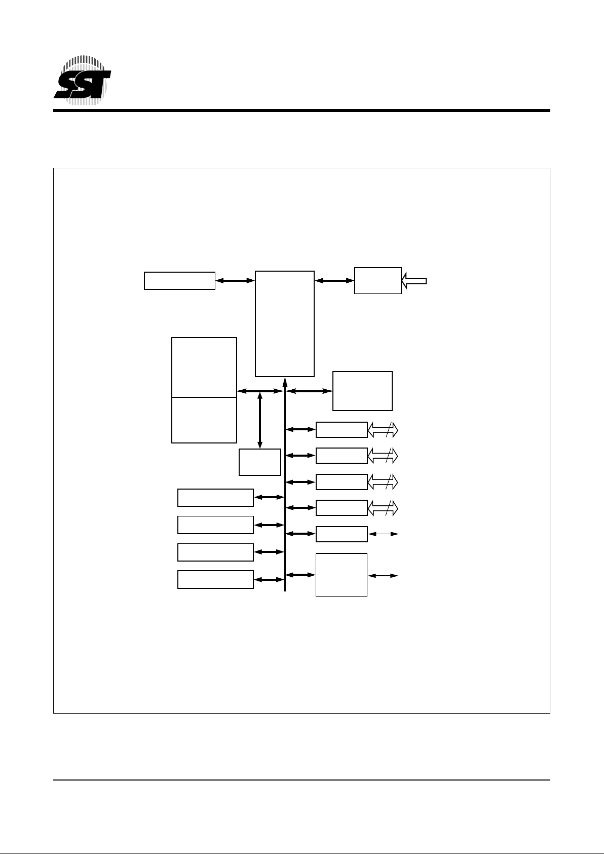
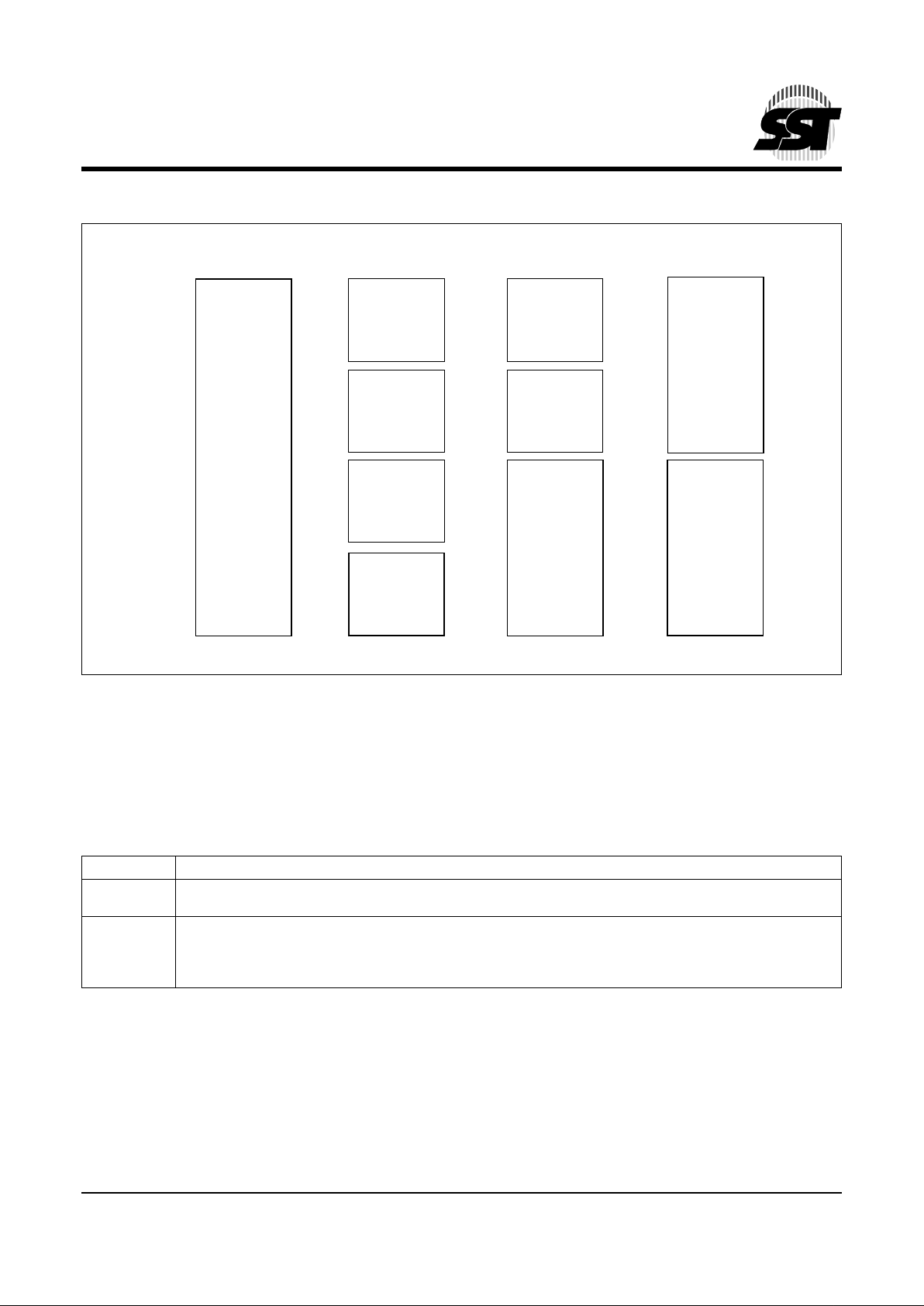
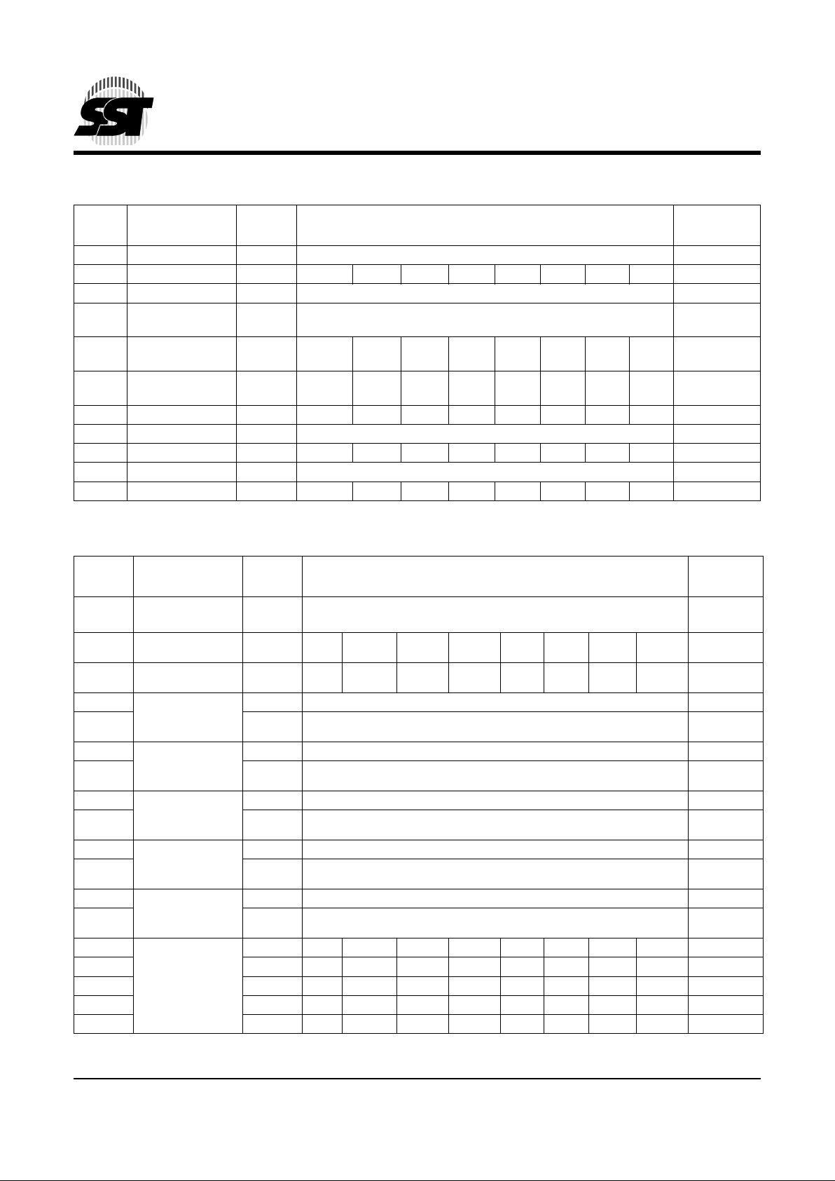
1.0 FUNCTIONAL BLOCKS
9 Interrupts
SuperFlash
EEPROM
Primary
Block
32K/64K x8
1
Secondary
Block
8K x8
I/O
I/O
I/O
I/O
Watchdog Timer
Interrupt
Control
8051
CPU Core
RAM
1K x8
Security
Lock
I/O Port 0
I/O Port 1
I/O Port 2
I/O Port 3
8-bit
Enhanced
UART
SPI
Timer 0 (16-bits)
Timer 1 (16-bits)
Timer 2 (16-bits)
88
8
8
555 ILL B1.0
PCA
1. 64K x8 for SST89E564RD and SST89V564RD
32K x8 for SST89E554RC and SST89V554RC
FUNCTIONAL BLOCK DIAGRAM
Page 7
Preliminary Specifications
FlashFlex51 MCU
SST89E564RD / SST89V564RD / SST89E554RC / SST89V554RC
7
©2001 Silicon Storage Technology, Inc. S71207-00-000 9/01 555
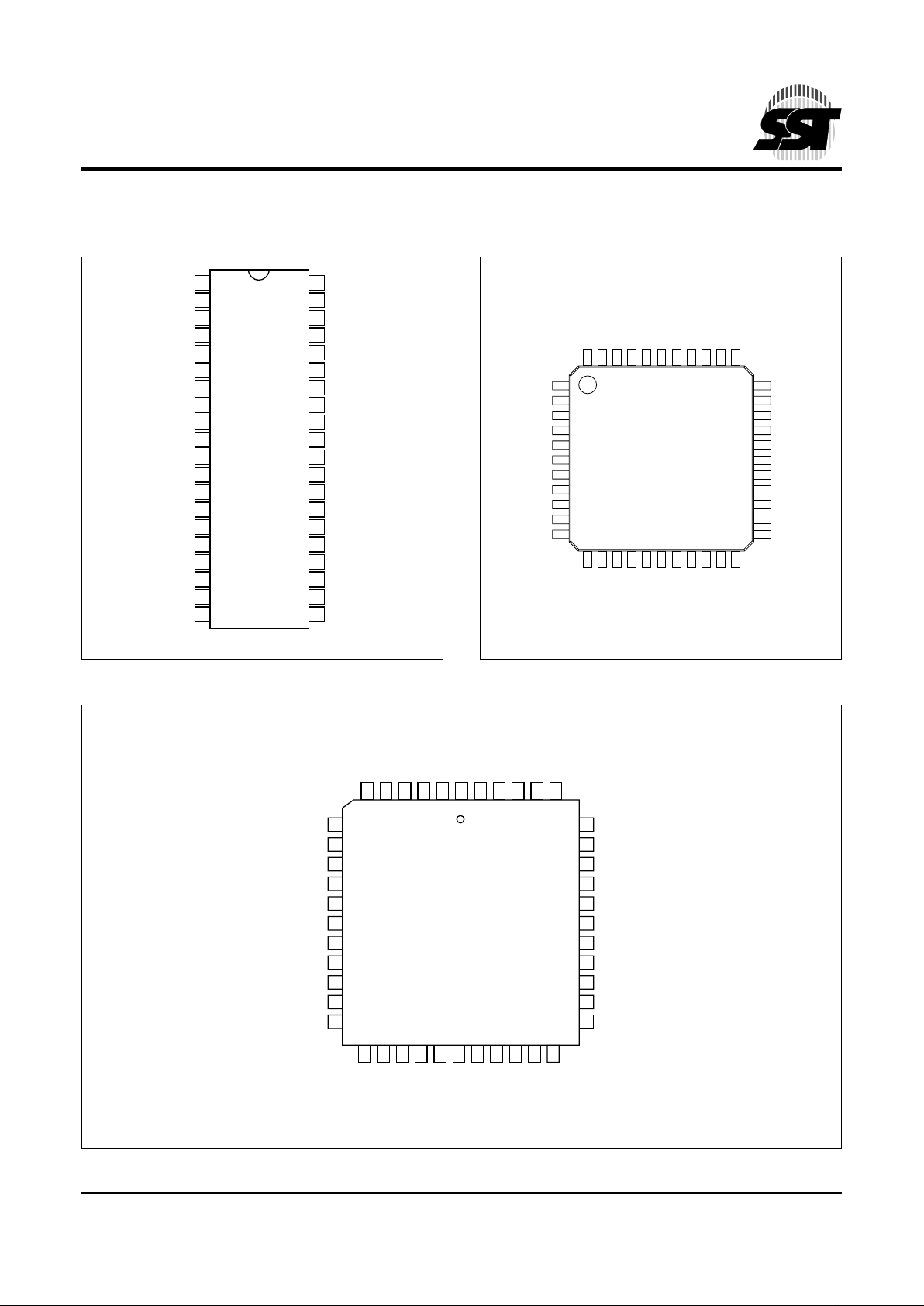
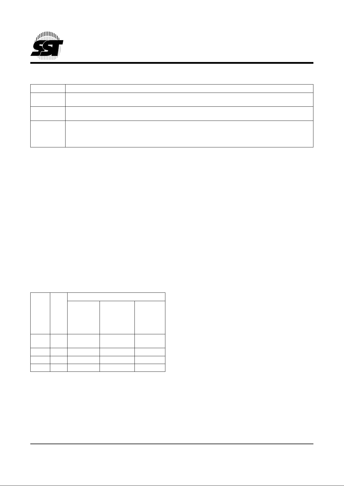
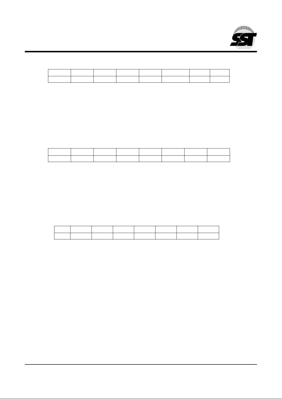
2.0 PIN ASSIGNMENTS
FIGURE 2-1: PIN ASSIGNMENTS FOR 40-PIN PDIP FIGURE 2-2: PIN ASSIGNMENTS FOR 44-LEAD TQFP
FIGURE 2-3: P
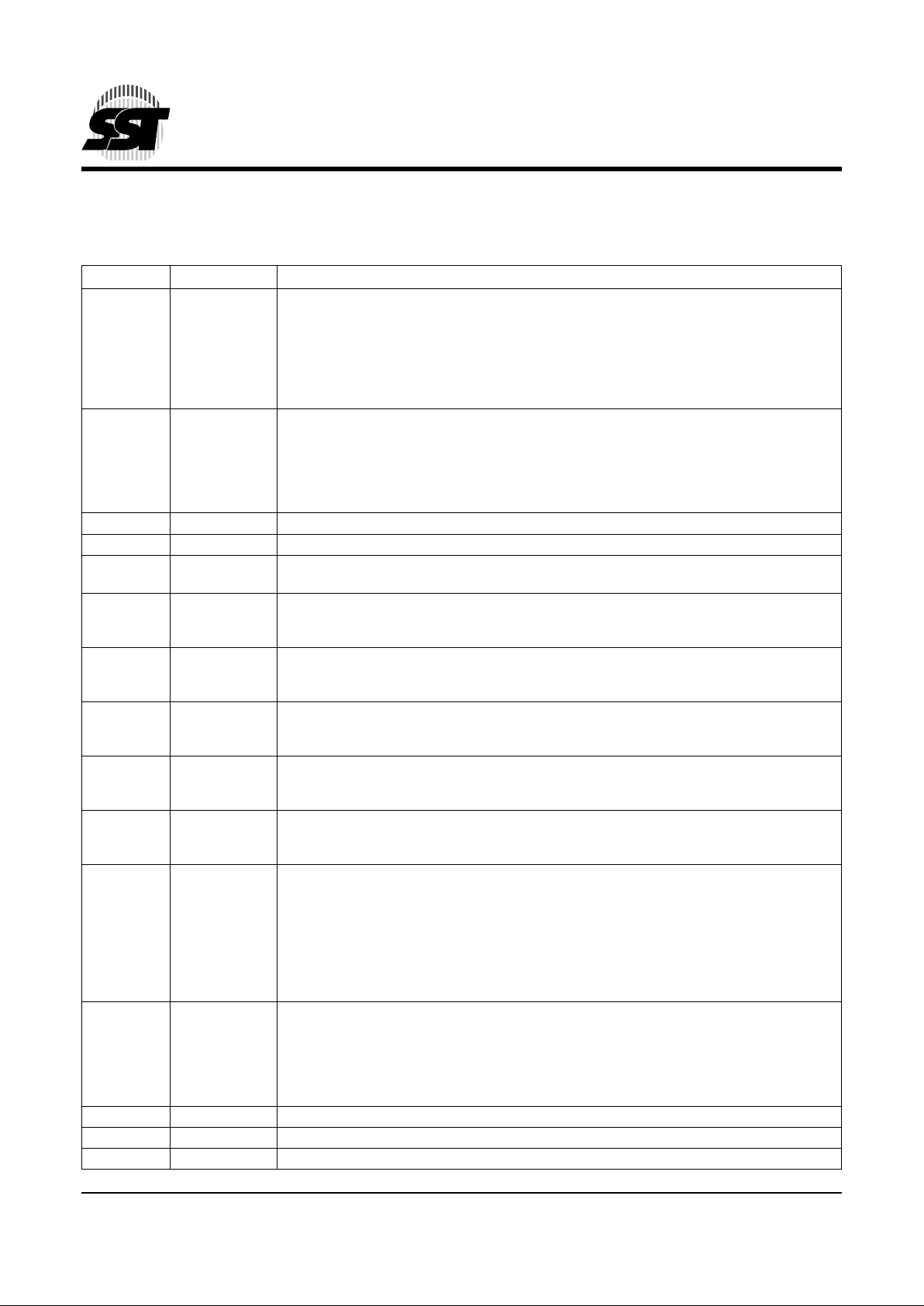
IN ASSIGNMENTS FOR 44-LEAD PLCC
40
39
38
37
36
35
34
33
32
31
30
29
28
27
26
25
24
23
22
21
(T2) P1.0
(T2 Ex) P1.1
P1.2
P1.3
(SS#) P1.4
(MOSI) P1.5
(MISO) P1.6
(SCK) P1.7
RST
(RXD) P3.0
(TXD) P3.1
(INT0#) P3.2
(INT1#) P3.3
(T0) P3.4
(T1) P3.5
(WR#) P3.6
(RD#) P3.7
XTAL2
XTAL1
V
SS
1
2
3
4
5
6
7
8
9
10
11
12
13
14
15
16
17
18
19
20
V
DD
P0.0 (AD0)
P0.1 (AD1)
P0.2 (AD2)
P0.3 (AD3)
P0.4 (AD4)
P0.5 (AD5)
P0.6 (AD6)
P0.7 (AD7)
EA#
ALE/PROG#
PSEN#
P2.7 (A15)
P2.6 (A14)
P2.5 (A13)
P2.4 (A12)
P2.3 (A11)
P2.2 (A10)
P2.1 (A9)
P2.0 (A8)
40-pin PDIP
T op View
555 ILL F1a.0
(MOSI) P1.5
(MISO) P1.6
(SCK) P1.7
RST
(RXD) P3.0
Reserved
(TXD) P3.1
(INT0#) P3.2
(INT1#) P3.3
(T0) P3.4
(T1) P3.5
P0.4 (AD4)
P0.5 (AD5)
P0.6 (AD6)
P0.7 (AD7)
EA#
Reserved
ALE/PROG#
PSEN#
P2.7 (A15)
P2.6 (A14)
P2.5 (A13)
P1.4 (SS#)
P1.3
P1.2
P1.1 (T2 Ex)
P1.0 (T2)
Reserved
VDDP0.0 (AD0)
P0.1 (AD1)
P0.2 (AD2)
P0.3 (AD3)
(WR#) P3.6
(RD#) P3.7
XTAL2
XTAL1
V
SS
Reserved
(A8) P2.0
(A9) P2.1
(A10) P2.2
(A11) P2.3
(A12) P2.4
555 ILL F1b.0
1
2
3
4
5
6
7
8
9
10
11
33
32
31
30
29
28
27
26
25
24
23
44 43 42 41 40 39 38 37 36 35 34
12 13 14 15 16 17 18 19 20 21 22
44-lead TQFP
T op View
39
38
37
36
35
34
33
32
31
30
29
7
8
9
10
11
12
13
14
15
16
17
(MOSI) P1.5
(MISO) P1.6
(SCK) P1.7
RST
(RXD) P3.0
Reserved
(TXD) P3.1
(INT0#) P3.2
(INT1#) P3.3
(T0) P3.4
(T1) P3.5
P0.4 (AD4)
P0.5 (AD5)
P0.6 (AD6)
P0.7 (AD7)
EA#
Reserved
ALE/PROG#
PSEN#
P2.7 (A15)
P2.6 (A14)
P2.5 (A13)
6 5 4 3 2 1 44 43 42 41 40
18 19 20 21 22 23 24 25 26 27 28
P1.4 (SS#)
P1.3
P1.2
P1.1 (T2 Ex)
P1.0 (T2)
Reserved
VDDP0.0 (AD0)
P0.1 (AD1)
P0.2 (AD2)
P0.3 (AD3)
(WR#) P3.6
(RD#) P3.7
XTAL2
XTAL1
V
SS
Reserved
(A8) P2.0
(A9) P2.1
(A10) P2.2
(A11) P2.3
(A12) P2.4
44-lead PLCC
T op Vie w
555 ILL F01c.0
Page 8
8
Preliminary Specifications
FlashFlex51 MCU
SST89E564RD / SST89V564RD / SST89E554RC / SST89V554RC
©2001 Silicon Storage Technology, Inc. S71207-00-000 9/01 555
2.1 Pin Descriptions
TABLE 2-1: PIN DESCRIPTIONS (1 OF 2)
Symbol Type
1
Name and Functions
P0[7:0] I/O Port 0: Port 0 is an 8-bit open drain bi-directional I/O port. As an output port each pin can
sink several LS TTL inputs. Port 0 pins float that have “1”s written to them, and in this state
can be used as high-impedance inputs. Port 0 is also the multiplexed low-order address and
data bus during accesses to external memory. In this application, it uses strong internal pullups when transitioning to V
OH
. Port 0 also receives the code bytes during the external host
mode programming, and outputs the code bytes during the external host mode verification.
External pull-ups are required during program verific ation.
P1[7:0] I/O with internal
pull-ups
Port 1: Port 1 is an 8-bit bi-directional I/O port with internal pull-ups. The P o rt 1 output buff ers
can drive LS TTL inputs. Port 1 pins are pulled high by the internal pull-ups when “1”s are
written to them and can be used as inputs in this state. As inputs, Port 1 pins that are externally pulled low will so urce cu rrent (I
IL
, see Tables 11-3 and 11-4 ) beca use of t he inte rnal pullups. P1[5, 6, 7] have high current drive of 16 mA. Port 1 also receives the low-order address
bytes during the external host mode programming and verif ication.
P1[0] I/O T2: External count input to Timer/Counter 2 or Clock-out from Timer/Counter 2
P1[1] I T2EX: Timer/Counter 2 capture/reload trigger and direction control
P1[2] I ECI: PCA Timer/Counter External Input:
This signal is the external clock input for the PCS timer/counter.
P1[3] I/O CEX0: Compare/Capture Module External I/O
Each compare/capture module connects to a Port 1 pin for external I/O. When not used by
the PCA, this pin can handle standard I/O.
P1[4] I/O SS#: Master Input or Slave Output for SPI.
OR
CEX1: Compare/Capture Module External I/O
P1[5] I/O MOSI: Master Output line, Slave Input line for SPI
OR
CEX2: Compare/Capture Module External I/O
P1[6] I/O MISO: Master Input line, Slave Output line for SPI
OR
CEX3: Compare/Capture Module External I/O
P1[7] I/O SCK: Master clock output, slave clock input line for SPI
OR
CEX4: Compare/Capture Module External I/O
P2[7:0] I/O with internal
pull-ups
Port 2: Port 2 is an 8-bit bi-directional I/O port with internal pull-ups. Port 2 pins are pulled
high by the internal pull-ups when “1”s are written to them and can be used as inputs in this
state. As inputs, Port 2 pins that are externally pulled low will source current (I
IL
, see Tables
11-3 and 11-4) because of the internal pull-ups. Port 2 sends the high-order address byte
during fetches from exte rnal Program me mory and during acce sses to e xternal Data Mem ory
that use 16-bit address (MOVX@DPTR). In this application, it uses strong internal pull-ups
when transitioning to V
OH
. Port 2 also receives some control signals and a partial of high-
order address bits during the external host mode programming and verification.
P3[7:0] I/O with internal
pull-ups
Port 3: Port 3 is an 8-bit bidirecti onal I/O port with internal pull-ups. The P ort 3 output buffers
can drive LS TTL inputs. Port 3 pins are pulled high by the internal pull-ups when “1”s are
written to them and can be used as inputs in this state. As inputs, Port 3 pins that are externally pulled low will so urce cu rrent (IIL, see Tables 11-3 and 11-4 ) beca use of t he inte rnal pullups. P ort 3 also receives some control signals and a partial of high-order addre ss bits during
the external host mode programming and verification.
P3[0] I RXD: Serial input line
P3[1] O TXD: Serial output lin e
P3[2] I INT0#: External Interrupt 0 Input
Page 9
Preliminary Specifications
FlashFlex51 MCU
SST89E564RD / SST89V564RD / SST89E554RC / SST89V554RC
9
©2001 Silicon Storage Technology, Inc. S71207-00-000 9/01 555
P3[3] I INT1#: External Interrupt 1 Input
P3[4] I T0: External count input to Timer/Counter 0
P3[5] I T1: External count input to Timer/Counter 1
P3[6] O WR#: External Data Memory Write strobe
P3[7] O RD#: External Data Memory Read strobe
PSEN# I/O Program Store Enable: PSEN# is the Read strobe to External Program Store. When the
device is executing from Internal Program Memory, PSEN# is inactive (V
OH
). When the
device is executing code from External Program Memory, PSEN# is activated twice each
machine cycle, ex ce pt whe n acce ss to Exte rnal Data Memory while one PSEN# activation is
skipped in each machine cycle. A forced high-to-low input transition on the PSEN# pin while
the RST input is continually held high for more than ten mac hin e c yc les wil l ca us e the device
to enter External Host mode for programming.
RST I Reset: Whil e the oscill ator is running, a hi gh logic sta te on this pin for tw o machine c ycles will
reset the device. After a reset, if the PSEN# pin is driven by a high-to-low input transition
while the RST input pin is held high, the device will enter the Exter nal Host mode, otherwise
the device will enter the Normal operation mode.
EA# I External Access Enable: EA# must be driven to V
IL
in order to enable the device to fetch
code from the External Program Memory. EA# must be driven to V
IH
for internal program execution. However, Security lock level 4 will disable EA#, and program execution is only possible from internal program memory. The EA# pin can tolerate a high voltage2 of 12V
(see “Absolute Maximum Stress Ratings” on page 51).
ALE/PROG# I/O Address Latch Enable: ALE is the output signal for latching the low byte of the address dur-
ing access es to external memor y. This pin is also the programming pulse input (PROG#) for
the external host mode. ALE is activated twice each machine cycle, except when access to
External Data Memory, one ALE activation is skipped in th e seco nd mac hine cycl e . Ho wever,
if AO is set to 1, ALE is disabled. (see “Auxiliary Register (AUXR)” on page20)
XTAL1
XTAL2
I
O
Oscillator: Input and output to the inverting oscillator amplifier. XTAL1 is input to internal
clock generation circuits from an external clock source.
V
DD
I Power Supply: Supply voltage during normal, Idle, Power Down, and Standby Mode opera-
tions.
V
SS
I Ground: Circuit ground. (0V reference)
T2-1.0 555
1. I = Input; O = Output
2. It is not necessary to receive a 12V programming supply voltage during flash programming.
TABLE 2-1: PIN DESCRIPTIONS (CONTINUED) (2 OF 2)
Symbol Type
1
Name and Functions
Page 10
10
Preliminary Specifications
FlashFlex51 MCU
SST89E564RD / SST89V564RD / SST89E554RC / SST89V554RC
©2001 Silicon Storage Technology, Inc. S71207-00-000 9/01 555
3.0 MEMORY ORGANIZATION
The device has separate addr e ss s pa ces for program an d
data memory.
3.1 Program Memory
There are two internal flash memor y blocks in the device.
The primary flash memory block (Block 0) has 64/32
KByte. The secondary flash memory block (Block 1) has 8
KByte. Since the total program address space is limited to
64/32 KByte, the SFCF[1:0] bit are used to control Program
Bank Selectio n. Please re fer to Figure 3-1 and F igure 3-2
for the program memory configurations. Program Bank
Select is described in the next section.
The 64K/32K x8 primary SuperFlash block is organized as
512/256 sectors, each sector consists of 128 Bytes.
The 8K x8 secondary SuperFlash block is organized as 64
sectors, each sector consists also of 128 Bytes.
For both blocks, the 7 least significant program address bits
select the byte within the sector. The remainder of the program addr ess bits selec t the sect or with in the b loc k.
FIGURE 3-1: P
ROGRAM MEMORY ORGANIZATION FOR SST89E564RD AND SST89V564RD
555 ILL F02.0
External
64 KByte
EA# = 0
FFFFH
0000H
64 KByte
Block 0
EA# = 1
SFCF[1:0] = 01, 10, 11
FFFFH
0000H
56 KByte
Block 0
8 KByte
Block 1
EA# = 1
SFCF[1:0] = 00
FFFFH
2000H
0000H
1FFFH
Page 11
Preliminary Specifications
FlashFlex51 MCU
SST89E564RD / SST89V564RD / SST89E554RC / SST89V554RC
11
©2001 Silicon Storage Technology, Inc. S71207-00-000 9/01 555
FIGURE 3-2: PROGRAM MEMORY ORGANIZATION FOR SST89E554RC AND SST89V554RC
3.2 Program Memory Block Switching
The program memory block s wit ch in g feature of the device
allows either Block 1 or the lowest 8 KByte of Block 0 to be
used for the lowest 8 KByte of the program address space.
SFCF[1:0] controls program memory block switching.
555 ILL F03.2
External
64 KByte
EA# = 0
FFFFH
0000H
32 KByte
Block 0
EA# = 1
SFCF[1:0] = 10, 11
FFFFH
0000H
24 KByte
Block 0
8 KByte
Block 1
8 KByte
Block 1
EA# = 1
SFCF[1:0] = 00
FFFFH
2000H
7FFFH
8000H
DFFFH
E000H
DFFFH
E000H
7FFFH
8000H
0000H
1FFFH
External
24 KByte
8 KByte
Block 1
External
24 KByte
External
32 KByte
EA# = 1
SFCF[1:0] = 01
FFFFH
7FFFH
8000H
0000H
32 KByte
Block 0
TABLE 3-1: SFCF VALUES FOR P ROGRAM MEMORY BLOCK SWITCHING FOR SST89E564RD/SST89V564RD
SFCF[1:0] Program Memory Block Switching
01, 10, 11 Block 1 is not visible to the PC;
Block 1 is reacha ble only via In-Application Programming from 000H - 1FFFH.
00 Block 1 is overlaid onto the low 8K of the program address space; occupying address locations 0000H - 1FFFH.
When the PC falls within 0000H - 1FFFH, the instruction will be fetched from Block 1 instead of Block 0.
Outside of 0000H - 1FFFH, Block 0 is used. Locations 0000H - 1FFFH of Block 0 are reachable through
In-Application Programming.
T3-1.0 555
Page 12
12
Preliminary Specifications
FlashFlex51 MCU
SST89E564RD / SST89V564RD / SST89E554RC / SST89V554RC
©2001 Silicon Storage Technology, Inc. S71207-00-000 9/01 555
3.2.1 Reset Configuration of Program Memory
Block Switching
Program memor y block switching is initialized after reset
according to the state of the Start-up Configuration bit SC0.
The SC0 bit is programmed via an External Host Mode
command or an IAP Mode command. Se e Table 4-2 and
Table 4-6.
Once out of reset, the SFCF[0] bit can be changed dynamically by th e progr am f or desir ed eff ects . Changing SFCF[0]
will not change the SC0 bit.
Caution must be taken when dynamically changing the
SFCF[0] bit. Since this will cause different physical memory
to be mapped to t he logical program address s pace. The
user must avoid executing block switching instructions
within the address range 0000H to 1FFFH.
3.3 Data Memory
The device has 1024 x8 bits of on-chip RAM and can
address up to 64 KByte of external data memory.
The device has f our sect ions of internal dat a memory:
1. The lower 128 Bytes of RAM (00H to 7FH) are
directly and indirectly addressable.
2. The higher 128 Bytes of RAM (80H to FFH) are
indirectly addressable.
3. The Special Function Registers (SFRs, 80H to
FFH) are directly addressable only.
4. The expanded RAM of 768 Bytes (00H to 2FFH) is
indirectly addressable by the move external
instruction (MOVX) and clearing the EXTRAM bit.
(See “Auxiliary Register (AUXR)” on page 20)
3.4 Dual Data Pointers
The device has two 16-bit data pointers. The DPTR Select
(DPS) bit in AUXR1 determines which of the two data
pointers is accessed. When DPS=0, DPTR0 is selected;
when DPS=1, DPTR1 is selected. Quickly switching
between the two data pointers can be accomplished by a
single INC instruction on AUXR1.
3.5 Special Function Registers (SFR)
Most of the unique features of the Flash Flex51 microcontroller family are contr o ll ed by bits i n s pe ci al fun c tio n r eg isters (SFRs) located in the SFR Memory Map shown in
Table 3-4. Individual descriptions of each SFR are provided
and Reset values indicated in T ables 3-5 to 3-9.
TABLE 3-2: SFCF V
ALUES FOR PROGRAM MEMORY BLOCK SWITCHING FOR SS T8 9E554RC/SST 89V 554RC
SFCF[1:0] Program Memory Block Switching
10, 11 Block 1 is not visible to the PC;
Block 1 is reachable only via In-Application Programming from E000H - FFFFH.
01 Both Block 0 and Block 1 are visible to the PC.
Block 0 is occupied from 0000H - 7FFFH. Block 1 is occupied from E000H - FFFFH.
00 Block 1 is overlaid onto the low 8K of the program address space; occupying address locations 0000H - 1FFFH.
When the PC falls within 0000H - 1FFFH, the instruction will be fetched from Block 1 instead of Block 0.
Outside of 0000H - 1FFFH, Block 0 is used. Locations 0000H - 1FFFH of Block 0 are reachable through
In-Application Programming.
T3-2.0 555
TABLE 3-3: SFCF VALUES UNDER DIFFERENT
R
ESET CONDITIONS
SC1
1
1. SC1 only applies to SST89E554RC and SST89V554RC.
SC0
State of SFCF[1:0] after:
Power-on
or
External
Reset
WDT
Reset
or
Brown-out
Reset
Software
Reset
11 00
(default)
x0 10
10 01 x1 11
0 1 10 10 10
0 0 11 11 11
T3-3.0 555
Page 13
Preliminary Specifications
FlashFlex51 MCU
SST89E564RD / SST89V564RD / SST89E554RC / SST89V554RC
13
©2001 Silicon Storage Technology, Inc. S71207-00-000 9/01 555
TABLE 3-4: FLASHFLEX51 SFR MEMORY MAP
8 BYTES
F8H IPA
1
CH CCAP0H CCAP1H CCAP2H CCAP3H CCAP4H FFH
F0H B
1
IPAH F7H
E8H IEA
1
CL CCAP0L CCAP1L CCAP2L CCAP3L CCAP4L EFH
E0H ACC
1
E7H
D8H CCON
1
CMOD CCAPM0 CCAPM1 CCAPM2 CCAPM3 CCAPM4 DFH
D0H PSW
1
SPCR D7H
C8H T2CON
1
T2MOD RCAP2L RCAP2H TL2 TH2 CFH
C0H WDTC
1
C7H
B8H IP
1
SADEN BFH
B0H P3
1
SFCF SFCM SFAL SFAH SFDT SFST IPH B7H
A8H IE
1
SADDR SPSR AFH
A0H P2
1
AUXR1 A7H
98H SCON
1
SBUF 9FH
90H P1
1
97H
88H TCON
1
TMOD TL0 TL1 TH0 TH1 AUXR 8FH
80H P0
1
SP DPL DPH WDTD SPDR PCON 87H
T3-4.1 555
1. SFRs are bit addressable.
Page 14
14
Preliminary Specifications
FlashFlex51 MCU
SST89E564RD / SST89V564RD / SST89E554RC / SST89V554RC
©2001 Silicon Storage Technology, Inc. S71207-00-000 9/01 555
TABLE 3-5: CPU RELATED SFRS
Symbol Description
Direct
Address
Bit Address, Symbol, or Alternative Port Function
RESET
ValueMSB LSB
ACC
1
Accumulator E0H ACC[7:0] 00H
B
1
B Register F0H B[7:0] 00H
PSW
1
Program Status
Word
D0H CY AC F0 RS1 RS0 OV F1 P 00H
SP Stack Pointer 81H SP[7:0] 07H
DPL Data Pointer
Low
82H DPL[7:0] 00H
DPH Data Pointer
High
83H DPH[7:0] 00H
IE
1
Interrupt Enable A8H EA EC ET2 ES0 ET1 EX1 ET0 EX0 40H
IEA
1
Interrupt
Enable A
E8H - - - - EBO - - - xxxx0xxxb
IP
1
Interrupt Priority
Reg
B8H - PPC PT2 PS PT1 PX1 PT0 PX0 x0000000b
IPH Interrupt Priority
Reg High
B7H - PPCH PT2H PSH PT1H PX1H PT0H PX0H x0000000b
IPA
1
Interrupt Priority
Reg A
F8H - - - - PBO - - - xxxx0xxxb
IPAH Interrupt Priority
Reg A High
F7H - - - - PBO
H
- - - xxxx0xxxb
PCON Power Control 87H SMOD1 SMOD0 BOF POF GF1 GF0 PD IDL 00010000b
AUXR Auxiliary Reg 8EH - - - - - - EXTRAM AO xxxxxxx00b
AUXR1 Auxiliary Reg 1 A2H - - - - GF2 0 - DPS xxxx00x0b
T3-5.1 555
1. Bit Addressable SFRs
TABLE 3-6: FLASH MEMORY PROGRAMMING SFRS
Symbol Description
Direct
Address
Bit Address, Symbol, or Alternative Port Function
RESET
ValueMSB LSB
SFST SuperFlash
Status
B6H SECD1 SECD2 SECD3 - - FLASH_BUSY - - xxxxx0xxb
SFCF SuperFlash
Configuration
B1H - IAPEN - - - - SWR BSEL x0xxxxxxb
SFCM SuperFlash
Command
B2H FIE FCM 00H
SFDT SuperFlash
Data
B5H SuperFlash Data Register 00H
SFAL SuperFlash
Address Low
B3H SuperFlash Low Order Byte Address Register - A
7
to A0 (SFAL) 00H
SFAH SuperFlash
Address High
B4H SuperFlash High Order Byte Address Register - A
15
to A8 (SFAH) 00H
T3-6.0 555
Page 15
Preliminary Specifications
FlashFlex51 MCU
SST89E564RD / SST89V564RD / SST89E554RC / SST89V554RC
15
©2001 Silicon Storage Technology, Inc. S71207-00-000 9/01 555
TABLE 3-7: WATCHDOG TIMER SFRS
Symbol Description
Direct
Address
Bit Address, Symbol, or Alternative Port Function
RESET
ValueMSB LSB
WDTC
1
Watchdog Timer
Control
C0H - - - WDOUT WDRE WDTS WDT SWDT xxx00x00b
WDTD Watchdog Timer
Data/Reload
85H Watchdog Timer Data/Reload 00H
T3-7.0 555
1. Bit Addressable SFRs
TABLE 3-8: TIMER/COUNTERS SFRS
Symbol Description
Direct
Address
Bit Address, Symbol, or Alternative Port Function
RESET
ValueMSB LSB
TMOD Timer/Counter
Mode Control
89H Timer 1 Timer 0 00H
GATE C/T# M1 M0 GATE C/T# M1 M0
TCON
1
1. Bit Addressable SFRs
Timer/Counter
Control
88H TF1 TR1 TF0 TR0 IE1 IT1 IE0 IT0 00H
TH0 Timer 0 MSB 8CH TH0[7:0] 00H
TL0 Timer 0 LSB 8AH TL0[7:0] 00H
TH1 Timer 1 MSB 8DH TH1[7:0] 00H
TL1 Timer 1 LSB 8BH TL1[7:0] 00H
T2CON
1
Timer / Counter 2
Control
C8H TF2 EXF2 RCLK TCLK EXEN2 TR2 C/T2# CP/RL2# 00H
T2MOD# Timer2
Mode Control
C9H---- - -T2OEDCENxxxxxx00b
TH2 Timer 2 MSB CDH T H2[7:0] 00H
TL2 Timer 2 LSB CCH TL2[7:0] 00H
RCAP2H Timer 2 Capture MSB CBH RCAP2H[7:0] 00H
RCAP2L Timer 2 Capture LSB CAH RCAP2L[7:0] 00H
T3-8.0 555
Page 16
16
Preliminary Specifications
FlashFlex51 MCU
SST89E564RD / SST89V564RD / SST89E554RC / SST89V554RC
©2001 Silicon Storage Technology, Inc. S71207-00-000 9/01 555
TABLE 3-9: INTERFACE SFRS
Symbol Description
Direct
Address
Bit Address, Symbol, or Alternative Port Function
RESET
ValueMSB LSB
SBUF Serial Data Buffer 99H SBUF[7:0] Indeterminate
SCON
1
Serial Port Control 98H SM0/FE SM1 SM2 REN TB8 RB8 TI RI 00H
SADDR Slave Address A9H SADDR#[7:0] 00H
SADEN Slave Address
Mask
B9H SADEN#[7:0] 00H
SPCR SPI Control
Register
D5H SPIE SPE DORD MSTR CPOL CPHA SPR1 SPR0 04H
SPSR SPI Status
Register
AAH SPIF WCOL 00H
SPDR SPI Data Register 86H SPD7 SPD6 SPD5 SPD4 SPD3 SPD2 SPD1 SPD0 00H
P0
1
Port 0 80H P0[7:0] FFH
P1
1
Port 1 90H - - - - - - T2EX T2 FFH
P2
1
Port 2 A0H P2[7:0] FFH
P3
1
Port 3 B0H RD# WR# T1 T0 INT1# INT0# TXD RXD FFH
T3-9.0 555
1. Bit Addressable SFRs
TABLE 3-10: PCA SFRS
Symbol Description
Direct
Address
Bit Address, Symbol, or Alternative Port Function
RESET
ValueMSB LSB
CH
CL
PCA Timer/Counter
F9H
E9H
CH[7:0]
CL[7:0]
00H
00H
CCON
1
1. Bit Addressable SFRs
PCA Timer/Counter
Control Register
D8H CF CR - CCF4 CCF3 CCF2 CCF1 CCF0 00x00000b
CMOD
PCA Timer/Counter
Mode Register
D9H CIDL WDTE - - - CPS1 CPS0 ECF 00xxx000b
CCAP0H PCA Module 0
Compare/Capture
Registers
FAH CCAP0H[7:0] 00H
CCAP0L EAH CCAP0L[7:0] 00H
CCAP1H PCA Module 1
Compare/Capture
Registers
FBH CCAP1H[7:0] 00H
CCAP1L EBH CCAP1L[7:0] 00H
CCAP2H PCA Module 2
Compare/Capture
Registers
FCH CCAP2H[7:0] 00H
CCAP2L ECH CCAP2L[7:0] 00H
CCAP3H PCA Module 3
Compare/Capture
Registers
FDH CCAP3H[7:0] 00H
CCAP3L EDH CCAP3L[7:0] 00H
CCAP4H PCA Module 4
Compare/Capture
Registers
FEH CCAP4H[7:0] 00H
CCAP4L EEH CCAP4L[7:0] 00H
CCAPM0 PCA
Compare/Capture
Module Mode
Registers
DAH - ECOM0 CAPP0 CAPN0 MAT0 TOG0 PWM0 ECCF0 x000 0000b
CCAPM1 DBH - ECOM1 CAPP1 CAPN1 MAT1 TOG1 PWM1 ECCF1 x000 0000b
CCAPM2 DCH - ECOM2 CAPP2 CAPN2 MAT2 TOG2 PWM2 ECCF2 x000 0000b
CCAPM3 DDH - ECOM3 CAPP3 CAPN3 MAT3 TOG3 PWM3 ECCF3 x000 0000b
CCAPM4 DEH - ECOM4 CAPP4 CAPN4 MAT4 TOG4 PWM4 ECCF4 x000 0000b
T3-10.1 555
Page 17
Preliminary Specifications
FlashFlex51 MCU
SST89E564RD / SST89V564RD / SST89E554RC / SST89V554RC
17
©2001 Silicon Storage Technology, Inc. S71207-00-000 9/01 555
Symbol Function
SECD1 Security bit 1.
SECD2 Security bit 2.
SECD3 Security bit 3.
Please refer to Table 4-6 for security lock options.
FLASH_BUSY Flash operation completion polling bit.
1: Device is busy with flash operation.
0: Device has fully completed the last command.
Symbol Function
IAPEN Enable IAP operation
0: IAP commands are disabled
1: IAP commands are enabled
SWR Software Reset
See “10.2 Software Reset” on page 47
BSEL Program memory block switching bit
See Figures 3-1 and 3-2.
Symbol Function
FIE Flash Interrupt Enable.
0: INT1# is not reassigned.
1: INT1# is re-assigned to signal IAP operation completion.
External INT1# interrupts are ignored.
FCM[6:0] Flash operation command
000_1011b Sector-Erase
000_1101b Block-Erase
000_1100b Byte-Verify
1
000_1110b Byte-Program
000_1111b Prog-SB1
000_0011b Prog-SB2
000_0101b Prog-SB3
000_1001b Prog-SC0
All other combinations are not implemented, and reserved for future use.
1. Byte-Verify has a single machine cycle latency and will not generate any INT1# interrupt regardless of
FIE.
SuperFlash Status Register (SFST) (Read Only Register)
Location76543 2 10Reset Value
0B6H SECD1 SECD2 SECD3 - -
FLASH_BUSY
- - xxxxx0xxb
SuperFlash Configuration Register (SFCF)
Location76543210Reset Value
0B1H - IAPEN ----
SWR BSEL
x0xxxxxxb
SuperFlash Command Register (SFCM)
Location76543210Reset Value
0B2H FIE FCM6 FCM5 FCM4 FCM3 FCM2 FCM1 FCM0 00000000b
Page 18
18
Preliminary Specifications
FlashFlex51 MCU
SST89E564RD / SST89V564RD / SST89E554RC / SST89V554RC
©2001 Silicon Storage Technology, Inc. S71207-00-000 9/01 555
Symbol Function
SFDT Mailbox register for interfacing with flash memory block. (Data register).
Symbol Function
SFAL Mailbox register for interfacing with flash memory block. (Low order address register).
Symbol Function
SFAH Mailbox register for interfacing with flash memory block. (High order address register).
Symbol Function
EA Global Interrupt Enable.
0 = Disable
1 = Enable
EC PCA Interrupt Enable.
ET2 Timer 2 Interrupt Enable.
ES Serial Interru pt Enable.
ET1 Timer 1 Interrupt Enable.
EX1 External 1 Interrupt Enable.
ET0 Timer 0 Interrupt Enable.
EX0 External 0 Interrupt Enable.
Symbol Function
EBO Brown-out Interrupt Enable.
1 = Enable the interrupt
0 = Disable the interrupt
SuperFlash Data Register (SFDT)
Location76543210Reset Value
0B5H SuperFlash Data Register 00000000b
SuperFlash Address Registers (SFAL)
Location76543210Reset Value
0B3H SuperFlash Low Order Byte Address Register 00000000b
SuperFlash Address Registers (SFAH)
Location76543210Reset Value
0B4H SuperFlash High Order Byte Address Register 00000000b
Interrupt Enable (IE)
Location76543210Reset Value
A8H EA EC ET2 ES ET1 EX1 ET0 EX0 00H
Interrupt Enable A (IEA)
Location76543210Reset Value
E8H----EBO---xxxx0xxxb
Page 19
Preliminary Specifications
FlashFlex51 MCU
SST89E564RD / SST89V564RD / SST89E554RC / SST89V554RC
19
©2001 Silicon Storage Technology, Inc. S71207-00-000 9/01 555
Symbol Function
PPC PCA interrupt priority bit.
PT2 Timer 2 interrupt priority bit.
PS Serial Port interr upt pr iority bit.
PT1 Timer 1 interrupt priority bit.
PX1 External interrupt 1 priority bit.
PT0 Timer 0 interrupt priority bit.
PX0 External interrupt 0 priority bit.
Symbol Function
PPCH PCA interrupt priority bit high.
PT2H Timer 2 interrupt priority bit high.
PSH Serial Port interrupt priority bit high.
PT1H Timer 1 interrupt priority bit high.
PX1H External interrupt 1 priority bit high.
PT0H Timer 0 interrupt priority bit high.
PX0H External interrupt 0 priority bit high.
Symbol Function
PBO Brown-out interrupt priority bit.
Symbol Function
PBOH Brown-out Interrupt priority bit high.
Interrupt Priority (IP)
Location76543210Reset Value
B8H - PPC PT2 PS PT1 PX1 PT0 PX0 x0000000b
Interrupt Priority High (IPH)
Location76543210Reset Value
B7H - PPCH PT2H PSH PT1H PX1H PT0H PX0H x0000000b
Interrupt Priority A (IPA)
Location76543210Reset Value
F8H----PBO---xxxx0xxxb
Interrupt Priority A High (IPAH)
Location76543210Reset Value
F7H----PBOH---xxxx0xxxb
Page 20

20
Preliminary Specifications
FlashFlex51 MCU
SST89E564RD / SST89V564RD / SST89E554RC / SST89V554RC
©2001 Silicon Storage Technology, Inc. S71207-00-000 9/01 555
Symbol Function
EXTRAM 0: Internal Expanded RAM access. For details, refer to “Data Memory” on page 12.
1: External data memory access.
AO 0: Normal ALE
1: ALE is normally off. ALE is active only during a MOVX or MOVC instruction. This will reduce
EMI.
Symbol Function
GF2 General purpose user-defined fla g.
DPS DPTR registers select bit.
0: DPTR0 is selected.
1: DPTR1 is selected.
Symbol Function
WDOUT Watchdog output enable.
0: Watchdog reset will not be exported on Reset pin.
1: Watchdog reset if enabled by WDRE, will assert Reset pin for 32 clocks.
WDRE Watchdog timer reset enable.
0: Disable watchdog timer reset.
1: Enable watchdog timer reset.
WDTS Watchdog timer reset flag.
0: External hardware reset clears the flag.
Flag can also be cleared by writing a 1.
Flag survives if chip reset happened because of watchdog timer overflow.
1: Hardware sets the flag on watchdog overflow.
WDT Watchdog timer refresh.
0: Hardware resets the bit when refresh is done.
1: Software sets the bit to force a watchdog timer refresh.
SWDT Start watchdog timer.
0: Stop WDT.
1: Start WDT.
Auxiliary Register (AUXR)
Location76543210Reset Value
8EH------EXTRAMAOxxxxxx00b
Auxiliary Register 1 (AUXR1)
Location76543210Reset Value
A2H----GF20-DPSxxxx00x0b
Watchdog Timer Control Register (WDTC)
Location76543210Reset Value
0C0H---WDOUT
WDRE WDTS WDT SWDT xxx00x00b
Page 21

Preliminary Specifications
FlashFlex51 MCU
SST89E564RD / SST89V564RD / SST89E554RC / SST89V554RC
21
©2001 Silicon Storage Technology, Inc. S71207-00-000 9/01 555
Symbol Function
WDTD Initial/Reload value in Watchdog Timer. New value won’t be effective until WDT is set.
Symbol Function
CF PCA Timer/Counter Overflow Flag:
Set by hardware when the PCA timer/counter rolls over. This generates an interrupt
request if the ECF interrupt enable bit in CMOD is set. CF can be set by hardware or
software but can be cleared only by software.
CR PCA Timer/Counter Run Control Bit:
Set and Cleared by software to turn the PCA timer/counter on and off.
CCF[4:0] PCA Module Compare/Capture Flags:
Set by hardware when a match or capture occurs. This generates a PCA interrupt
request if the ECCFx interrupt enable bit in the corresponding CCAPMx register is set.
Must be cleared by software.
Symbol Function
CIDL PCA Timer/Counter Idle Control:
0: Allows the PCA timer/counter to run during idle mode.
1: Disables the PCA timer/counter during idle mode.
WDTE Watchdog Timer Enable:
0: Disables the PCA watchdog timer output.
1: Enables the PCA watchdog timer output on PCA module 4.
CPS1,CPS0 PCA Timer/Counter Input Select:
ECF PCA Timer/Counter Interrupt Enable:
0: Disables the CF bit in the CCON register.
1: Enables the CF bit in the CCON register to generate an interrupt request.
Watchdog Timer Data/Reload Register (WDTD)
Location76543210Reset Value
085H Watchdog Timer Data/Reload 00000000b
PCA Timer/Counter Control Register (CCON)
Location76543210Reset Value
D8H CF
CR - CCF4
CCF3 CCF2 CCF1 CCF0 00x00000b
PCA Timer/Counter Mode Register (CMOD)
Location76543210Reset Value
D9H CIDL
WDTE - -
- CPS1 CPS0 ECF 00xxx000b
CPS1 CPS0
0
0
1
1
0
1
0
1
f
OSC
/12
f
OSC
/4
Timer 0 overflow
External clock at ECI pin (maximum rate = f
OSC
/8)
Page 22

22
Preliminary Specifications
FlashFlex51 MCU
SST89E564RD / SST89V564RD / SST89E554RC / SST89V554RC
©2001 Silicon Storage Technology, Inc. S71207-00-000 9/01 555
TABLE 3-11: PCA MODULE MODES
ECOMy1CAPPy1CAPNy1MATy1TOGy1PWNy1ECCFy1Module Code
0 0 0 0 0 0 0 No Operation
- 1 0 0 0 0 - 16-bit capture on positive-edge trigger at CEX[4:0]
- 0 1 0 0 0 - 16-bit capture on negative-edge trigger at CEX[4:0]
- 1 1 0 0 0 - 16-bit capture on positive-/negative-edge trigger
at CEX[4:0]
1 0 0 1 0 0 - Compare: software timer
1 0 0 1 1 0 - Compare: high-speed output
1 0 0 0 0 1 0 Compare: 8-bit PWM
1 0 0 1 - 0 - Compare: PCA WDT (CCAPM4 only)
2
T3-11.0 555
1. y = 0, 1, 2, 3, 4
2. For PCA WDT mode, also set the WDTE bit in the CMOD register to enable the reset output signal
Page 23

Preliminary Specifications
FlashFlex51 MCU
SST89E564RD / SST89V564RD / SST89E554RC / SST89V554RC
23
©2001 Silicon Storage Technology, Inc. S71207-00-000 9/01 555
Symbol Function
ECOM[4:0] Compare Modes:
0: Disables the module comparator function.
1: Enables the module comparator function. The comparator is used to implement the
software timer, high-speed output, pulse width modulation, and watchdog timer modes.
CAPP[4:0] 0: Disables the capture function with capture triggered by a positive edge on pin
CEX[4:0].
1: Enables the capture function with capture triggered by a positive edge on pin
CEX[4:0].
CAPN[4:0] 0: Disables the capture function with capture triggered by a negative edge on pin
CEX[4:0].
1: Enables the capture function with capture trigg er ed by a negative edge on pin
CEX[4:0].
MAT[4:0] Match: Set ECOM[4:0] and MAT[4:0] to implement the software timer mode.
0: Disable the software timer mode
1: A match of the PCA timer/counter with the compare/capture register sets the
CCF[4:0] bit in the CCON register, flagging an interrupt.
TOG[4:0] Toggle: Set ECOM[4:0], MAT[4:0], and TOG[4:0] to implement the high-speed output
mode.
0: Disable the toggle function
1: A match of the PCA timer/counter with the compare/capture register toggles the
CEX[4:0] pin.
PWM[4:0] Pulse Width Modulation Mode:
0: Disable the pulse width modulation mode
1: Configures the module for operation as an 8-bit pulse width modulator with output
waveform on the CEX[4:0] pin.
ECCF[4:0] Enable CCF[4:0] Interrupt:
0: Disables compare/capture flag CCF[4:0] in the CCON register to generate an
interrupt request.
1: Enables compare/capture flag CCF[4:0] in the CCON register to generate an
interrupt request.
PCA Compare/Capture Module Mode Register (CCAPM[4:0])
Location76543210Reset Value
DAH -
ECOM0 CAPP0 CAPN0
MAT0 TOG0 PWM0 ECCF0 x0000000b
DBH -
ECOM1 CAPP1 CAPN1
MAT1 TOG1 PWM1 ECCF1 x0000000b
DCH -
ECOM2 CAPP2 CAPN2
MAT2 TOG2 PWM2 ECCF2 x0000000b
DDH -
ECOM3 CAPP3 CAPN3
MAT3 TOG3 PWM3 ECCF3 x0000000b
DEH -
ECOM4 CAPP4 CAPN4
MAT4 TOG4 PWM4 ECCF4 x0000000b
Page 24

24
Preliminary Specifications
FlashFlex51 MCU
SST89E564RD / SST89V564RD / SST89E554RC / SST89V554RC
©2001 Silicon Storage Technology, Inc. S71207-00-000 9/01 555
Symbol Function
SPIE If both SPIE and ES are set to one, SPI interrupts are enabled.
SPE SPI enable bit.
0: Disables SPI.
1: Enables SPI and connects SS#, MOSI, MI SO , a nd SCK to pins P1[4], P1[ 5], P1[6] , P1[7].
DORD Data Transmission Order.
0: MSB first in data transmission.
1: LSB first in data transmission.
MSTR Master/Slave select.
0: Selects Slave mode.
1: Selects Master mode.
CPOL Clock Polarity
0: SCK is low when idle (Active High).
1: SCK is high when idle (Active Low).
CPHA Clock Phase control bit.
0: Shift triggered on the leading edge of the clock.
1: Shift triggered on the trailing edge of the clock.
SPR1, SPR0 SPI Clock Rate Select bits. These two bits control the SCK rate of the device
configured as master. SPR1 and SPR0 have no effect on the slave. The relationship
between SCK and the oscillator frequency, f
OSC
, is as follows:
Symbol Function
SPIF Upon completion of data transfer, this bit is set to 1. If SPIE =1 and ES =1, an interrupt
is then generated. T o clear, read SPSR and then access SPDR.
WCOL Set if the SPI data register is written to during data transfer. To clear, read SPSR and
then access SPDR.
SPI Control Register (SPCR)
Location76543210Reset Value
D5H SPIE
SPE DORD MSTR
CPOL CPHA SPR1 SPR0 00000100b
SPR1 SPR0 SCK = f
OSC
divided by
0
0
1
1
0
1
0
1
4
16
64
128
SPI Status Register (SPSR)
Location76543210Reset Value
AAH SPIF
WCOL - -
----00xxxxxxb
Page 25

Preliminary Specifications
FlashFlex51 MCU
SST89E564RD / SST89V564RD / SST89E554RC / SST89V554RC
25
©2001 Silicon Storage Technology, Inc. S71207-00-000 9/01 555
Symbol Function
SMOD1 Double Baud rate bit. If SMOD1 = 1, Timer 1 is used to generate the baud rate.
SMOD0 FE/SM0 Selection bit.
0: SCON[7] = SM0
1: SCON[7] = FE,
BOF Brown-out detection status bit, this bit will not be affected by any other reset. BOF
should be cleared by software. Power-on reset will also clear the BOF bit.
0: No Brown-out.
1: Brown-out occurred
POF Power-on reset status bit, this bit will not be affected by any other reset. POF should be
cleared by software.
0: No Power-on reset.
1: Power-on reset occurred
GF1 General-purpose flag bit.
GF0 General-purpose flag bit.
PD Power-down bit.
0: Power-down mode is not activated.
1: Activates Power-down mode.
IDL Idle mode bit.
0: Idle mode is not activated.
1: Activates Idle mode.
SPI Data Register (SPDR)
Location76543210Reset Value
86H SPD7
SPD6 SPD5 SPD4
SPD3 SPD2 SPD1 SPD0 00H
Power Control Register (PCON)
Location76543210Reset Value
87H SMOD1
SMOD0 BOF POF
GF1 GF0 PD IDL 00010000b
Page 26

26
Preliminary Specifications
FlashFlex51 MCU
SST89E564RD / SST89V564RD / SST89E554RC / SST89V554RC
©2001 Silicon Storage Technology, Inc. S71207-00-000 9/01 555
Symbol Function
FE Set SMOD0 = 1 to access FE bit.
0: No framing error
1: Framing Error. Set by receiver when an invalid stop bit is detected. This bit needs to
be cleared by software.
SM0 SMOD0 = 0 to access SM0 bit.
Serial Port Mode Bit 0
SM1 Serial Port Mode Bit 1
SM2 Enables the Automatic Address Recognition feature in Modes 2 or 3. If SM2 = 1 then RI
will not be set unless the received 9th data bit (RB8) is 1, indicating an address, and
the received byte is a Given or broadcast Address. In Mode 1, if SM2 = 1 then RI will
not be activated unless a valid stop bit was received, and the received byte is a Given
or Broadcast Address. In Mode 0, SM2 should be 0.
REN Enables serial reception.
0: to disable reception.
1: to enable reception.
TB8 The 9th data bit that will be transmitted in Modes 2 and 3. Set or clear by software as
desired.
RB8 In Modes 2 and 3, the 9th data bit that was received. In Mode 1, if SM2 - 0, RB8 is the
stop bit that was received. In Mode 0, RB8 is not used.
TI Transmit interrupt flag. Set by hardware at the end of the 8th bit time in Mode 0, or at
the beginning of the stop bit in the other modes, in any serial transmission, Must be
cleared by software.
RI Receive interrupt flag. Set by hardware at the end of the8th bit time in Mode 0, or
halfway through the stop bit time in the other modes, in any serial reception (except see
SM2). Must be cleared by software.
Serial Port Control Register (SCON)
Location76543210Reset Value
98H SM0/FE
SM1 SM2 REN
TB8 RB8 TI RI 00000000b
SM0 SM1 Mode Description Baud Rate
1
1. f
OSC
= oscillator frequency
000Shift Registerf
OSC
/6 (6 clock mode) or f
OSC
/
12 (12 clock mode)
0 1 1 8-bit UART Variable
1029-bit UARTf
OSC
/32 or f
OSC
/16 (6 clock
mode) or f
OSC
/64 or
f
OSC
/32 (12 clock mode)
1 1 3 9-bit UART Variable
Page 27

Preliminary Specifications
FlashFlex51 MCU
SST89E564RD / SST89V564RD / SST89E554RC / SST89V554RC
27
©2001 Silicon Storage Technology, Inc. S71207-00-000 9/01 555
4.0 FLASH MEMORY PROGRAMMING
The device internal fl ash memor y can be programmed or
erased usin g the f ollo win g two m ethod s:
• External Host Mode
• In-Application Programming (IAP) Mode
4.1 External Host Programming Mode
External Ho st Programming Mod e allows the user to pr ogram the Flash memory directly without using the CPU.
External Ho st Mode is entered by forcing PSEN# from a
logic high to a logic low while RST input is being held continuously high. The device will stay in External Host Mode
as long as RST = 1 and PSEN# = 0.
A Read-ID operation is necessary to “arm” the device in
External Host Mode, and no other External Host Mode commands can be enabled until a Read-ID is performed. In
External Host Mode, the internal Flash memory blocks are
accessed through the re-assigned I/ O port pins (see Figure
4-1 for details) b y an external host, such as a MCU programmer, a PCB tester or a PC-controlled dev elopment board.
Note: Symbol ⇓ signifies a negative pulse and the command is asserted during the low state of PROG#/ALE input. All other combinations of
the above input pins are invalid and may result in unexpected behaviors.
Note: V
IL
= Input Low Voltage; VIH = Input High Vo ltage; V
IH1
= Input High Voltage (XTAL, RST); X = Don’t care; AL = Address low order byte;
AH = Address high order byte; DI = Data Input; DO = Data Output
TABLE 4-1: EXTERNAL HOST MODE COMMANDS FOR SST89E564RD/SST89V 564RD
Operation RST PSEN#
PROG#/
ALE EA# P3[7] P3[6] P2[7] P2[6] P0[7:0]
P3[5:4]
P2[5:0] P1[7:0]
Read-ID V
IH1
V
IL
V
IH
V
IH
V
IL
V
IL
V
IL
V
IL
DO AH AL
Chip-Erase V
IH1
V
IL
⇓ V
IH
V
IH
V
IL
V
IL
V
IL
XX X
Block-Erase V
IH1
V
IL
⇓ V
IH
V
IH
V
IH
V
IL
V
IH
XX X
Sector-Erase V
IH1
V
IL
⇓ V
IH
V
IH
V
IL
V
IH
V
IH
XAHAL
Byte-Program V
IH1
V
IL
⇓ V
IH
V
IH
V
IH
V
IH
V
IL
DI AH AL
Byte-Verify (Read) V
IH1
V
IL
V
IH
V
IH
V
IH
V
IH
V
IL
V
IL
DO AH AL
Select-Block0 V
IH1
V
IL
⇓ V
IH
V
IH
V
Il
V
Il
V
IH
X55H X
Select-Block1 V
IH1
V
IL
⇓ V
IH
V
IH
V
Il
V
Il
V
IH
XA5H X
Prog-SC0 V
IH1
V
IL
⇓ V
IH
V
IH
V
IL
V
IL
V
IH
X5AH X
Prog-SB1 V
IH1
V
IL
⇓ V
IH
V
IH
V
IH
V
IH
V
IH
XX X
Prog-SB2 V
IH1
V
IL
⇓ V
IH
V
IL
V
IL
V
IH
V
IH
XX X
Prog-SB3 V
IH1
V
IL
⇓ V
IH
V
IL
V
IH
V
IL
V
IH
XX X
T4-1.0 555
Page 28

28
Preliminary Specifications
FlashFlex51 MCU
SST89E564RD / SST89V564RD / SST89E554RC / SST89V554RC
©2001 Silicon Storage Technology, Inc. S71207-00-000 9/01 555
Note: Symbol ⇓ signifies a negative pulse and the command is asserted during the low state of PROG#/ALE input.
All other combinations of the above input pins are invalid and may result in unexpected behaviors.
Note: V
IL
= Input Low Voltage; VIH = Input High Vo ltage; V
IH1
= Input High Voltage (XTAL, RST); X = Don’t care; AL = Address low order byte;
AH = Address high order byte; DI = Data Input; DO = Data Output; A[15:13] = 0xxb for Block 0 and A[15:13] = 111b for Block 1
FIGURE 4-1: I/O PIN ASSIGNMENTS FOR EXTERNAL HOST MODE
TABLE 4-2: EXTERNAL HOST MODE COMMANDS FOR SST89E554RC/SST89V 554RC
Operation RST PSEN#
PROG#/
ALE EA# P3[7] P3[6] P2[7] P2[6] P0[7:0]
P3[5:4]
P2[5:0] P1[7:0]
Read-ID V
IH1
V
IL
V
IH
V
IH
V
IL
V
IL
V
IL
V
IL
DO AH AL
Chip-Erase V
IH1
V
IL
⇓ V
IH
V
IH
V
IL
V
IL
V
IL
XX X
Block-Erase V
IH1
V
IL
⇓ V
IH
V
IH
V
IH
V
IL
V
IH
X A[15:13] X
Sector-Erase V
IH1
V
IL
⇓ V
IH
V
IH
V
IL
V
IH
V
IH
XAHAL
Byte-Program V
IH1
V
IL
⇓ V
IH
V
IH
V
IH
V
IH
V
IL
DI AH AL
Byte-Verify (Read) V
IH1
V
IL
V
IH
V
IH
V
IH
V
IH
V
IL
V
IL
DO AH AL
Prog-SC0 V
IH1
V
IL
⇓ V
IH
V
IH
V
IL
V
IL
V
IH
X5AH X
Prog-SC1 V
IH1
V
IL
⇓ V
IH
V
IH
V
IL
V
IL
V
IH
X AAH X
Prog-SB1 V
IH1
V
IL
⇓ V
IH
V
IH
V
IH
V
IH
V
IH
XX X
Prog-SB2 V
IH1
V
IL
⇓ V
IH
V
IL
V
IL
V
IH
V
IH
XX X
Prog-SB3 V
IH1
V
IL
⇓ V
IH
V
IL
V
IH
V
IL
V
IH
XX X
T4-2.0 555
Flash
Control Signals
Address Bus
A7-A0
Flash
Control Signals
Address Bus
A13-A8
Input/
Output
Data
Bus
Port 0
V
SS
XTAL1
XTAL2
Ready/Busy#
Port 3
V
DD
RST
Port 2
Port 1
EA# ALE /
PROG#
PSEN#
7
6
5
A15
A14
4
3
2
1
0
7
6
7
6
5
4
3
2
1
0
0
7
6
0
Address Bus
A15-A14
555 ILL F04.0
Page 29

Preliminary Specifications
FlashFlex51 MCU
SST89E564RD / SST89V564RD / SST89E554RC / SST89V554RC
29
©2001 Silicon Storage Technology, Inc. S71207-00-000 9/01 555
4.1.1 Product Identification
The Read-ID command accesses the Signature Bytes that
identify the device and the m anufacturer as SST. External
programmers primarily use these Sign ature Bytes in the
selection of programming algorithms. The Read-ID command is selected by the command c ode of 0H on P3[7:6]
and P2[7:6]. See Figure 4-2 for timing waveforms.
4.1.2 Arming Command
An arming command sequence must take place before
any External Host Mode sequence command is recognized by the device. This prevents accidental trigg ering of
External Host M ode Comman ds due to nois e or pro grammer error. The arming command is as follows:
1. PSEN# goes low while RST is high. This will get
the machine in External Host Mode, re-configuring
the pins, and turning on the on-chip oscillator.
2. A Read-ID command is issued, and after 1 ms the
External Host Mode commands can be issued.
After the above sequence, all other Exte rnal Host Mode
commands are enabled. Before the Read-ID command is
received, all other External Host Mode commands
received are igno red.
4.1.3 Detail Explanation of the External Host Mode
Commands
The External Host Mod e commands are Read-ID, ChipErase, Block-Erase, Sector-Erase, Byte-Program, ByteVerify, Prog-SB1, Prog-SB2, Prog-SB3, Prog-SC0, ProgSC1, Select-Block0, Select-Block1. See T abl es 4-1 and 4-2
for all signal logic assignments, Figure 4-1 for I/O pin
assignments, and Table 4-7 for the timing parameters. The
critical timing for all Erase and Program commands is generated by an on-chip flas h me mo ry controll er. The high-tolow transition of the PROG # signal initiates the Erase or
Program commands, which are synchronized internally.
The Read comman ds are asynchronous read s, independent of the PROG# signal level.
Following is a detailed description of the External Host
Mode commands:
The Select-Block0 com mand enables Block 0 to be programmed in Externa l Host Mode. Once this comm and is
ex e cu te d, al l su bs eq ue n t Ex te rnal Ho st Comm an ds wil l be
directed at Block 0. S ee Figure 4-3 for timing waveforms.
This command applies to SST89E564RD/
SST89V564RD only.
The Select-Block1 command enables Block 1 (8 KByte
Block) to be programmed. Once this command is executed, all subsequ ent External Host Command s that are
directed to the address range below 2000H will be directed
at Block 1. The Sele ct-Block1 command only af fects the
lowest 8 KByte of the program address space. For
addresses greater than or equal to 2000H, Block 0 is
accessed by default. Upon enter ing External Host Mode,
Block 1 is selected by default. Se e Figure 4-3 for timing
waveforms. This command applies to SST89E564RD/
SST89V564RD only.
The Chip-Erase, Block-Erase, and Sector-Erase commands are used for erasing all or part of the memory
array. Erased data bytes in the memory array will be
erased to FFH. Memory locations that are to be programmed must be in the erase d state pr ior to program ming.
The Chip-Erase command erases all bytes in both memory
blocks, regardless of any previous Select-Block0 or SelectBlock1 commands. Chip-Erase ignores the Security Lock
status and will erase the Security Lock, returning the device
to its Unlocked state. The Chip-Erase command will also
erase the SC0 bit. Upon c ompletion of Chip-Erase command, Block 1 will be the selected block. See Figure 4-4 for
timing waveforms.
The Block-Erase command erases all bytes in the selected
memory blocks. This command will not be executed if the
security lock is enabled. The selection of the memory block
to be erased is d etermined by t he prior execution Selec tBlock0 or Select-Block1 co mmand. Se e Figure 4-6 for the
timing waveforms.
The Sector-Erase c ommand erases all of the bytes in a
sector. The sector size for the flash memory is 128 By tes.
This command wi ll not be executed if the Sec urity lock is
enabled. See Figure 4-7 for timing waveforms.
The Byte-Program command is used for programming new
data into the memory array. Programming will not take
place if any security locks are enabled. Se e Figure 4-8 for
timing waveforms.
TABLE 4-3: S
IGNATURE BYTES
Address Data
Manufacturer’s ID 30H BFH
Device ID
SST89E564RD 31H 91H
SST89V564RD 31H 90H
SST89E554RC 31H 99H
SST89V554RC 31H 98H
T4-3.0 555
Page 30

30
Preliminary Specifications
FlashFlex51 MCU
SST89E564RD / SST89V564RD / SST89E554RC / SST89V554RC
©2001 Silicon Storage Technology, Inc. S71207-00-000 9/01 555
The Byte-Verify command allows the user to verify that the
device correctly performed an Erase or Program command. This command will be disabled if any sec u r it y l ocks
are enabled. See Figure 4-11 for timing waveforms.
The Prog-SB1, Prog-SB2, Prog-SB3 commands program
the security bits, the functions of these bits are described in
the Security Lock sec ti on an d al s o in Table 9-1. Once programmed, these bits can only be erased through a ChipErase command. See Figure 4-9 for timing waveforms.
Prog-SC0 comma nd pr ograms SC0 b it, whi ch de ter min es
the state of SFCF[0] out of reset. Once programmed, SC0
can only be re stored to a n erased state v ia a Chip- Erase
command. See Figure 4-10 for timing waveforms.
Prog-SC1 comma nd pr ograms SC1 b it, whi ch de ter min es
the state of SFCF[1] out of reset. Once programmed, SC1
can only be re stored to a n erased state v ia a Chip- Erase
command. See Figure 4-10 for timing waveforms. ProgSC1 is for SST89E554RC/SST89V554RC only.
4.1.4 External Host Mode Clock Source
In External Host Mode, an internal oscillator will provide
clocking for the device. The on-chip oscillator will be turned
on as the device enters External Host Mode; i.e. when
PSEN# goes low while RST is high. Dur ing Ex tern al Host
Mode, the CPU core is held in reset. Upon exit from External Host Mode, the internal oscillator is turned off.
4.1.5 Flash Operation Status Detection Via External
Host Handshake
The device provides two method s for an external host to
detect the completi on of a flash me mory operation to optimize the Program or Erase time. The e nd of a fla sh me mory operation cycle can be detected by:
1. monitoring the Ready/Busy# bit at P3[3];
2. monitoring the Data# Polling bit at P0[3].
4.1.5.1 Ready/Busy# (P3[3])
The progress of the flash memory programming can be
monitored by the Ready/Busy# output signal. P3[3] is
driven low, some time after ALE/PROG# goes low during a
flash memory operation to indicate the Busy# status of the
Flash Control Unit (FCU). P3[3] is driven high when the
Flash programming operation i s completed to indicate the
Ready status .
4.1.5.2 Data# Polling (P0[3])
During a Program operat ion, any attempts to read (Byt eVe rify), while the d evice is busy, will receive the complement of the data of the last byte loaded (logic low , i.e. “0” for
an erase) on P0[3] with the rest of the bits “0”. During a Program operation, the Byte-Verify command i s reading the
data of the last byte loade d, not the data at the address
specified.
4.1.6 Step-by-step instructions to perform
External Host Mode commands
To program data into the memory array, apply power
supply voltage (V
DD
) to VDD and RST pins, and per-
form the following steps:
1. Maintain RST high and set PSEN# from logic high
to low, in sequence according to the appropriate
timing diagram.
2. Raise EA# High (V
IH
).
3. Issue Read-ID command to enable the External
Host Mode.
4. Verify that the memory blocks or sectors for programming is in the erased state, FFH. If they are
not erased, then erase them using the appropriate
Erase command.
5. Select the memory location using the address
lines (P3[5:4], P2[5:0], P1[7:0]).
6. Present the data in on P0[7:0].
7. Pulse ALE/PROG#, observing minimum pulse
width.
8. Wait for low to high transition on READY/BUSY#
(P3[3]).
9. Repeat steps 5 - 8 until programming is finished.
10. Verify the flash memory contents.
Page 31

Preliminary Specifications
FlashFlex51 MCU
SST89E564RD / SST89V564RD / SST89E554RC / SST89V554RC
31
©2001 Silicon Storage Technology, Inc. S71207-00-000 9/01 555
4.1.7 Flash Memory Pr ogramming Timing Diagrams with External Host Mode
FIGURE 4-2: R
EAD-ID
Reads chip signature and identification registers at the addressed location.
FIGURE 4-3: S
ELECT-BLOCK1 / SELECT-BLOCK0
Enables the selection of either of the flash memor y blocks prior to issuing a Byte-Verify, B lock-Erase, SectorErase, or Byte-Program. These commands apply to SST89E564RD/SST89V564RD only.
555 ILL F05.1
0030H
T
SU
T
ES
RST
PSEN#
ALE/PROG#
EA#
P3[5:4] ,P2[5:0] ,P1
P2[7:6] ,P3[7:6]
P0
0000b
T
RD
BFH
0031H
0000b
T
RD
Device ID
Device ID = 91H for SST89E564RD
90H for SST89V564RD
99H for SST89E554RC
98H for SST89V554RC
RST
PSEN#
ALE/PROG#
EA#
P3[3]
P3[5:4], P2[5:0] A5H/55H
T
PSB
T
PROG
T
ADS
555 ILL F06.1
P3[7:6], P2[7:6]
1001b
T
DH
T
SU
T
ES
Page 32

32
Preliminary Specifications
FlashFlex51 MCU
SST89E564RD / SST89V564RD / SST89E554RC / SST89V554RC
©2001 Silicon Storage Technology, Inc. S71207-00-000 9/01 555
FIGURE 4-4: CHIP-ERAS E
Erases both flash memory blocks. Security lock is ignored and the security bits are erased too.
FIGURE 4-5: B
LOCK-ERASE FOR SST89E56 4RD/SST89V 564RD
Erases one of the flash memory blocks, if the security lock is not activated on that flash memory block.
RST
PSEN#
ALE/PROG#
P3[3]
P3[7:6], P2[7:6]
0001b
T
CE
T
PROG
T
ADS
555 ILL F07.1
T
ES
T
SU
T
DH
EA#
RST
PSEN#
ALE/PROG#
P3[3]
P3[7:6], P2[7:6] 1101b
T
BE
T
PROG
T
SU
T
ADS
555 ILL F08.1
T
ES
T
DH
EA#
Page 33

Preliminary Specifications
FlashFlex51 MCU
SST89E564RD / SST89V564RD / SST89E554RC / SST89V554RC
33
©2001 Silicon Storage Technology, Inc. S71207-00-000 9/01 555
FIGURE 4-6: BLOCK-ERASE FOR SST89E554RC/SST89V554RC
Erases one of the flash memory blocks, if the security lock is not activated on that flash memory block.
FIGURE 4-7: S
ECTOR-ERASE
Erases the addressed sector if the security lock is not activated on that flash memory block.
RST
PSEN#
ALE/PROG#
P3[3]
P3[7:6], P2[7:6]
P3[5:4], P2[5:0]
1101b
AH
T
BE
T
PROG
T
SU
T
ADS
555 ILL F09.1
T
ES
T
DH
EA#
RST
PSEN#
ALE/PROG#
P3[3]
P3[7:6], P2[7:6]
P3[5:4], P2[5:0]
1011b
AH
T
SE
T
PROG
T
ADS
555 ILL F10.1
P1
AL
T
DH
T
SU
T
ES
EA#
Page 34

34
Preliminary Specifications
FlashFlex51 MCU
SST89E564RD / SST89V564RD / SST89E554RC / SST89V554RC
©2001 Silicon Storage Technology, Inc. S71207-00-000 9/01 555
FIGURE 4-8: BYTE-PROGRAM
Programs the addressed cod e byte if the byte location has been s uccessfully erased and not yet programmed.
Byte-Program operation is only allowed when the security lock is not activated on that flash memory block.
FIGURE 4-9: P
ROG-SB1 / PROG-SB2 / PROG-SB3
Programs the Security bits SB1, SB2 and SB3 respectively. Only a Chip-Erase will erase a programmed security bit.
RST
PSEN#
ALE/PROG#
EA#
P3[3]
P3[5:4], P2[5:0]
P1
AH
AL
T
PS
T
PROG
T
ADS
555 ILL F11.1
P0
P3[7:6], P2[7:6]
DI
1110b
T
DH
T
SU
T
ES
RST
PSEN#
ALE/PROG#
EA#
P3[3]
T
PS
T
PROG
T
ADS
555 ILL F12.1
P3[7:6], P2[7:6]
1111b / 0011b / 0101b
T
DH
T
SU
T
ES
Page 35

Preliminary Specifications
FlashFlex51 MCU
SST89E564RD / SST89V564RD / SST89E554RC / SST89V554RC
35
©2001 Silicon Storage Technology, Inc. S71207-00-000 9/01 555
FIGURE 4-10: PROG-SC0 / PROG-SC1
Programs the star t-up configuration bit SC0/SC1. O nly a Chip-Erase will erase a programmed SC0/SC1 bit.
Prog-SC1 applies to SST89E5 54RC/SST89V554RC only.
FIGURE 4-11: B
YTE-VERIFY
Reads the code byte from the addres sed flas h memory location if the sec ur ity lock is not activated on that fl ash
memory block.
RST
PSEN#
ALE/PROG#
EA#
P3[3]
P3[5:4], P2[5:0] 5AH / AAH
T
PS
T
PROG
T
ADS
555 ILL F13.1
P3[7:6], P2[7:6]
1001b
T
DH
T
SU
T
ES
555 ILL F14.1
P3[5:4], P2[5:0]
AL
DO
1100b
P3[7:6], P2[7:6]
T
SU
RST
PSEN#
ALE/PROG#
EA#
P0
P1
T
ALA
T
OA
T
AHA
AH
T
ES
Page 36

36
Preliminary Specifications
FlashFlex51 MCU
SST89E564RD / SST89V564RD / SST89E554RC / SST89V554RC
©2001 Silicon Storage Technology, Inc. S71207-00-000 9/01 555
4.2 In-Application Programming Mode
The device offers either 72 or 40 KB yte of In-Application
Programmable flash memory. During In-Application Programming, the CPU of the microcontroller enters IAP
Mode. The two blocks of flash me mory allow the CPU to
execute user code from one block, while the other is being
erased or reprogrammed concu rrentl y. The CPU may also
fetch code from an external memory while all internal flash
is being reprogrammed. The mailbox registers (SFST,
SFCM, SFAL, SF AH, SFDT and SFCF) located in the Special Function Register (SFR), control and monitor the
device’s erase and program process.
Table 4-6 outlines the commands and their associated
mailbox re gister settings .
4.2.1 In-Application Programming Mode Clock
Source
During IAP Mode, both the CPU core and the flash controller unit are dri ven off th e exter nal clock. However, an internal oscillator will provide timing references for Program and
Erase operations. The inte rnal oscill ator is only tur ned on
when required, and is turned off as soon as the Flash operation is compl eted.
4.2.2 Memory Bank Selection for In-Application
Programming Mode
With the addressing ran ge limited to 16 bit, only 64 KByte
of program address spac e is “visible” at any o ne time. As
shown in Ta ble 4-4, Bank Selection (the c onfiguration of
EA# and SFCF[1:0]), allows Block 1 memory to be overlaid
on the lowest 8 KByte of B lo ck 0 m em ory, making Block 1
reachable. The same c oncept is employed to allow both
Block 0 and Block 1 Flash to be acces sible to IAP operations. C ode fr om a b lock that is not visibl e may not be used
as a source to program another address. However, a block
that is not “visible” may be programm ed by code from th e
other block through mailbox registers.
The device allows IAP code in one block of memory to program the other block of memory, but may not program any
location in the sam e block. If an IAP operation origi nates
physically from Block 0, the target of this operation is implicitly defined to be in Blo ck 1. If the IAP op eratio n or igin ates
physically from Block 1, then the target address is implicitly
defined to be in Block 0. If the IAP operation originates from
External program space, then, the target will depend on the
address and the state of Bank Select.
4.2.3 IAP Enable Bit
The IAP Enable Bit, SFCF[6], e nables In-Application Pr ogramming mode. Until this bi t is set all flash pr ogramming
IAP commands will be ignored.
4.2.4 In-Application Programming Mode Commands
All of the following commands can only be initiated in the
IAP Mode. In all situations, wri ting the control byte to the
SFCM register will initiate all of the operations. All commands will not be enabled if the security locks are enabled
on the selected me mory bloc k.
The Program command is for programming new data int o
the memory array. The portion of the memory array to be
programmed should be in the erased state, FFH. If the
memory is not erased, it should first be erased with an
appropriate Erase command. Warning: Do not attempt to
write (program or erase) to a block that the code is currently fetching from. This will cause unpredictable program behavior and may corrupt program data.
The Block-Erase command erase s all bytes in one of the
two memory blocks. The s electi on of the me mory block to
be erased is determined by the source of Block-Erase
Command, as defined in T ab le 4-4.
TABLE 4-4: IAP A
DDRESS RESOLUTION FOR SST89E564RD/SST89V564RD
EA# SFCF[1:0] Address of IAP Inst. Target Address Block Being Programmed
1 00 >= 2000H (Block 0) >= 2000H (Block 0) None
1
1. No operation is perfo rmed because code from one block may not program the same or iginating block
1 00 >= 2000H (Block 0) < 2000H (Block 1) Block 1
1 00 < 2000H (Block 1) Any (Block 0) Block 0
1 01, 10, 11 Any (Block 0) >= 2000H (Block 0) None
1
1 01, 10, 11 Any (Block 0) < 2000H (Block 1) Block 1
0 00 From external >= 2000H (Block 0) Block 0
0 00 From external < 2000H (Block 1) Block 1
0 01, 10, 11 From external Any (Block 0) Block 0
T4-4.0 555
Page 37

Preliminary Specifications
FlashFlex51 MCU
SST89E564RD / SST89V564RD / SST89E554RC / SST89V554RC
37
©2001 Silicon Storage Technology, Inc. S71207-00-000 9/01 555
The Sector-Erase c ommand erases all of the bytes in a
sector. The sector size for the flash memory Blocks is 128
Bytes. The selection of the sector to be erased is determined by the contents of SFAH and SF AL.
The Byte-Program comm and programs data into a sin gle
byte. The address is deter m ined by the contents of SFAH
and SFAL. The data byte is in SFDT .
The Byte-Verify command allows the user to verify that the
device has correctly performed an Erase or Program command.
Byte-Verify command returns th e data byte in S FDT if the
command is successful. The user is required to check that
the previous Flash operation has fully completed before
issuing a Byte- Verify. Byte -Verify comman d execution time
is short enough th at there is no need to poll for command
completion and no interrupt is generated.
Prog-SB3, Prog-SB2, Prog-SB1 commands are used to
program the Secur ity bits (see Table 9-1). Comple tion of
any of these commands, the security options will be
updated immediately.
Security bits previously in un-programmed state can be
programmed by these commands. Prog-SB3, Prog-SB2
and Prog-SB1 commands should only reside in Block 1.
Prog-SC0 comman d is used to p rogram the SC0 bi t. This
command only chang es the SC0 bit a nd has no effect on
BSEL bit until after a reset cycle.
SC0 bit previously in un-programmed state can be programmed by this command. The Prog-SC0 command
should reside only in Bl ock 1.
Prog-SC1 comman d is used to p rogram the SC1 bi t. This
command only chang es the SC1 bit a nd has no effect on
BSEL bit until after a reset cycle.
SC1 bit previously in un-programmed state can be programmed by this command. The Prog-SC1 command
should reside only in Block 1.
There are no IAP counterparts for the External Host commands Select-Block0 and Select-Block1.
4.2.5 Polling
A command that uses the polling method to detect flash
operation completi on s hould poll on the FLA SH_BUS Y bit
(SFST[2]). When FLASH_BUSY de-asserts (logic 0), the
device is ready for the next operation.
MOVC instruction may als o be used for verifi cation of th e
Programming and Erase operation of the flash memory.
MOVC instruction will fail if it is directed at a flash block that
is still busy.
4.2.6 Interrupt Termination
If interrupt ter mination is selected, (SFCM[7] is set), the n
an interrupt (INT1) will be generated to indicate flash operation completion. Under this condition, the INT1 becomes an
internal in terrupt s ource. The INT 1# pin can now be us ed
as a general purp ose po rt pin and it cann ot be the sourc e
of External Interrupt 1 during In-Application Programming.
In order to use an interrupt to signal flash operation termination. EX1 and E A bi ts of IE re gi ster mus t be s et. The IT1
bit of TCON register must also be set for edge trigger
detection.
.
Page 38

38
Preliminary Specifications
FlashFlex51 MCU
SST89E564RD / SST89V564RD / SST89E554RC / SST89V554RC
©2001 Silicon Storage Technology, Inc. S71207-00-000 9/01 555
.
TABLE 4-5: IN-APPLICATION PROGRAMMING MODE COMMANDS1 FOR SST89 E564RD/SST89V5 64RD
Operation SFCM [6:0]
2
SFDT [7:0] SFAH [7:0] SFAL [7:0]
Block-Erase
3
0DH 55H X
4
X
Sector-Erase
3
0BH X AH
5
AL
6
Byte-Program
3
0EH DI
7
AH AL
Byte-Verify (Read)
3
0CH DO
8
AH AL
Prog-SB1
9
0FH AAH X X
Prog-SB2
9
03H AAH X X
Prog-SB3
9
05H AAH X X
Prog-SC0
9
09H AAH 5AH X
T4-5.0 555
1. SFCF[6]=1 enables IAP commands; SFCF[6]=0 disables IAP commands.
2. Interrupt/Polling enable for flash operation completion
SFCM[7] =1: Interrupt enable for flash operation completion
0: polling enable for flash operation completion
3. Refer to Table 4-4 for address resolution
4. X can be V
IL
or VIH, but no other value.
5. AH = Address high order byte
6. AL = Address low order byte
7. DI = Data Input
8. DO = Data Output
All other values are in hex
9. Instruction must be located in Block 1
TABLE 4-6: IN-APPLICATION PROGRAMMING MODE COMMANDS1 FOR SST89 E554RC/SST89V5 54RC
1. SFCF[6]=1 enables IAP commands; SFCF[6]=0 disables IAP commands.
Operation SFCM [6:0]
2
2. Interrupt/Polling enable for flash operation completion
SFCM[7] =1: Interrupt enable for flash operation completion
0: polling enable for flash operation completion
SFDT [7:0] SFAH [7:0] SFAL [7:0]
Block-Erase
3
3. Refer to Table 4-4 for address resolution
0DH 55H AH
4
4. SFAH[7]=0: Selects Block 0; SFAH[7:5] = 111b selects Block 1
X
5
5. X can be VIL or VIH, but no other value.
Sector-Erase
3
0BH X AH
6
6. AH = Address high order byte
AL
7
7. AL = Address low order byte
Byte-Program
3
0EH DI
8
8. DI = Data Input
AH AL
Byte-Verify (Read)
3
0CH DO
9
9. DO = Data Output
All other values are in hex
AH AL
Prog-SB1
10
10. Instruction must be located in Block 1
0FH AAH X X
Prog-SB2
10
03H AAH X X
Prog-SB3
10
05H AAH X X
Prog-SC0
10
09H AAH 5AH X
Prog-SC1
10
09H AAH AAH X
T4-6.0 555
Page 39

Preliminary Specifications
FlashFlex51 MCU
SST89E564RD / SST89V564RD / SST89E554RC / SST89V554RC
39
©2001 Silicon Storage Technology, Inc. S71207-00-000 9/01 555
5.0 TIMERS/COUNTERS
The device has three 16 -bit regist ers that c an be used as
either timers or event counters. The three Timers/Counters
are denoted Timer 0 (T0), Ti mer 1 (T1) , and Time r 2 (T2).
Each is design ated a pair of 8-bit regi sters in the SFRs.
The pair consists of a most significant (high) byte and least
significant (low) byte. The respective registers are TL0,
TH0, TL1, TH1, TL2, and TH2.
6.0 SERIAL I/O
6.1 Enhanced Universal Asynchronous
Receiver/Transmitter (UART)
The device Serial I/O port is a full duplex port that allows
data to be transmitted and received simultaneously in
hardware by the transmit and receive registers, respectively, while the software is performing other tasks. The
transmit and receive registers are both located in the
Serial Data Buffer ( SBUF) special function register. Writing to the SBUF register loads the transmit register, and
reading from the SBUF register obtains the contents of
the receive regi ster.
The UART has four modes of operation which are selected
by the Serial Port Mode Specifier (SM0 and SM1) bits of
the Serial Port Control (SCON) special function register. In
all four modes, transmiss ion is initiated by any instructio n
that uses the SBUF register as a destination register.
Reception is initiated in mode 0 when the Receive Interrupt
(RI) flag bit of the Serial Port Control (SCON) SFR is
cleared and the Reception Enable/ Disable (REN) bit of the
SCON register is set. Reception is initiated in the other
modes by the incoming start bit if the REN bit of the SCON
register is set.
6.1.1 Framing Error Detection
Framing Error Detection allows the se rial p or t to au tomatically check for valid stop bits in Modes 1, 2 or 3. If
a stop bit is missing the Framing Error bit (F E) will be
set. The software can then check this bit after a reception to detect communication errors. The FE bit must
be cleared by software.
The FE bit is loc ated in SCON and shar es the same bit
address as SM0. The SMOD0 bit located in the PCON register determines which of these two bits is accessed. When
SMOD0 = 0, SCON[7] will act as SM0. When SMOD0 = 1,
SCON[7] will act as FE.
6.1.2 Automatic Address Recognition
Automatic Address Rec ognition (AAR) reduces the CP U
time required to ser vice th e seri al por t i n a multi processor
environment. When using AAR, the serial port hardware
will only generate an interrupt when it receives its own
address, thus eliminating the software overhead required to
compare addresses.
TABLE 4-7: F
LASH MEMORY PROGRAMMING/VERIFIC ATION PARAMETERS
Parameter
1,2
Symbol Min Max Units
Reset Setup Time T
SU
3µs
Read-ID Command Width T
RD
1 µs
PSEN# Setup Time T
ES
1.125 µs
Address, Command, Data Setup Time T
ADS
0ns
Chip-Erase Time T
CE
125 ms
Block-Erase Time T
BE
100 ms
Sector-Erase Time T
SE
30 ms
Program Setup Time T
PROG
1.2 µs
Address, Command, Data Hold T
DH
0ns
Byte-Program Time
3
T
PB
50 µs
Select-Block Program Time T
PSB
500 ns
Security bit Program Time T
PS
80 µs
Verify Command Delay Time T
OA
50 ns
Verify High Order Address Delay Time T
AHA
50 ns
V erify Lo w Ord er Addres s Delay Time T
ALA
50 ns
T4-7.0 555
1. Program and Erase times will scale inversely proportional to programming clock frequency.
2. All timing measurements are from the 50% of the input to 50% of the output.
3. Each byte must be erased before programming.
Page 40

40
Preliminary Specifications
FlashFlex51 MCU
SST89E564RD / SST89V564RD / SST89E554RC / SST89V554RC
©2001 Silicon Storage Technology, Inc. S71207-00-000 9/01 555
AAR is only available when using the serial port in either
mode 2 or 3. Setting the SM2 bit in SCON enables AAR.
Each slave must have its SM2 bit set when waiting for an
address (9th bi t = 1) . The R eceiv e Inte rrupt (R I) fla g will only
be set when the recei ved byte matche s eithe r the G iven or
Broadcast Address. The slave then clears its SM2 bit to
enable reception of data bytes (9th bit = 0) from the master.
The master can selectively communicate with groups of
slaves by sending the Given Address. Addressing all
slaves is also possible by sending the Broadcas t address.
The SADDR and SADEN special function registers define
these addresses for each slave.
SADDR specifies a s laves indivi dua l ad dr es s an d SA DE N
is a mask byte that defines don’t-care bits to form the Given
address when com bi ned with SADDR. The following is a n
exampl e:
In this example Slave 1 can be distinguished from Slave 2
by using bits 0 and 1. Slave 1 will not respond to an
address that ha s bi t 1 set to 1 wh ile Slave 2 will. S imila r ly,
Slave 2 will not respond to an address that has bit 0 set to 0
while Slave 1 will. Both slaves will respond to an address of
1111 0x01b so this is t he Broadc ast Addre ss. The Broa dcast Addresses is formed by the logical OR of SADDR and
SADEN with 0s treated as don’t-care bits.
6.2 Serial Peripheral Interface (SPI)
The device SPI allows for high-speed ful l-duplex synchronous data transfer between the device and o ther c ompat ible SPI devices.
Figure 6-1 shows the correspondence between master
and slave SPI devices. The SCK pin is the clock output and
input for the master and slave modes, respectively . The SPI
clock generator will start following a write to the master
devices SPI data register. The written d ata is then shi fted
out of the MOSI pin on the master device into the MOSI pin
of the slave device. Following a complete transmission of
one byte of data, the SPI clock generator i s stopped and
the SPIF flag is set. An SPI interrupt request will be generated if the SPI interrupt enable bit (SPIE) and the serial port
interrupt enable bit (ES) are both set.
An external master drives th e Slave Select inpu t pin, S S#/
P1[4], low to select the SPI module as a slave. If SS#/P1[4]
has not been driven low, then the slave SPI unit is not
active and the MOSI/P1[5] port can also be used as an
input port pin.
CPHA and CPOL control the phase and polarity of the SPI
clock. Figures 6-2 and 6-3 show the four possible combinations of these two bits.
FIGURE 6-1: SPI M
ASTER-SLAVE INTERCONNECTION
UART Slave 1
SADDR = 1111 0001
SADEN = 1111 1010
GIVEN = 1111 0x0x
UART Slave 2
SADDR = 1111 0011
SADEN = 1111 1001
GIVEN = 1111 0xx1
555 ILL F15.0
8-bit Shift Register
MSB MASTER LSB
SPI
Clock Generator
MISO MISO
MOSI MOSI
SCK SCK
SS# SS#
8-bit Shift Register
MSB SLAVE LSB
V
IH
Page 41

Preliminary Specifications
FlashFlex51 MCU
SST89E564RD / SST89V564RD / SST89E554RC / SST89V554RC
41
©2001 Silicon Storage Technology, Inc. S71207-00-000 9/01 555
FIGURE 6-2: SPI TRANSFER FORMAT WITH CPHA = 0
FIGURE 6-3: SPI TRANSFER FORMAT WITH CPHA = 1
555 ILL F16.0
MSB
SCK Cycle #
(for reference)
SCK (CPOL=0)
SCK (CPOL=1)
MOSI
(from Master)
MISO
(from Slave)
SS# (to Slave)
6
12345678
5
MSB
* Not defined, but normally MSB of next received byte
654321LSB
*
4 3 2 1 LSB
555 ILL F17.0
MSB
SCK Cycle #
(for reference)
SCK (CPOL=0)
SCK (CPOL=1)
MOSI
(from Master)
MISO
(from Slave)
SS# (to Slave)
6
12345678
5
MSB
* Not defined but normally LSB of previously transmitted character
654321 LSB
*
4 3 2 1 LSB
Page 42

42
Preliminary Specifications
FlashFlex51 MCU
SST89E564RD / SST89V564RD / SST89E554RC / SST89V554RC
©2001 Silicon Storage Technology, Inc. S71207-00-000 9/01 555
7.0 WATCHDOG TIMER
The devic e off ers a pro gram mable Wa tchdog Ti mer (WDT)
for fail safe protection against software deadl ock an d aut omatic recovery.
To protect the s ystem agai nst soft ware deadlock, the user
software must refresh the W DT w ithin a us er-d efine d tim e
period. If the software fails to do this periodi cal refresh , an
internal hardware reset will be initiated if enabled (WDRE=
1). The software can be designed such that the WDT times
out if the program does not work properly .
The WDT in the device uses the syste m clock (XTAL1) as
its time base. So strictly speaking, it is a watchdog counter
rather than a watchdog timer. The WDT registe r will i ncrement every 344064 cr ys tal clocks. The u pper 8-bi ts of th e
time base register (WDTD) are used as the reload register
of the WDT.
The WDTS flag bit is set by WDT overflow and is not
changed by WDT reset. User software can clear WDTS by
writing “1” to it.
Figure 7-1 provides a block diagram of the WDT . Two SFRs
(WDTC and WDTD) control watchdog timer operation.
During idle mode, WDT operation is temporarily suspended, and resumes upon an interrupt exit from idle.
The time-out period of the WDT is calculated as follows:
Period = (255 - WDT) * 344064 * 1/f
OSC
where WDT is the value loaded in to the WDT regi s ter an d
f
OSC
is the oscillator frequency.
FIGURE 7-1: B
LOCK DIAGRAM OF PROGRAMMA BLE WATCHDOG TIMER
555 ILL F18.0
WDT Upper Byte
WDT Reset
Internal Reset
344064
clks
Counter
CLK (XTAL1)
Ext. RST
WDTC
WDTD
Page 43

Preliminary Specifications
FlashFlex51 MCU
SST89E564RD / SST89V564RD / SST89E554RC / SST89V554RC
43
©2001 Silicon Storage Technology, Inc. S71207-00-000 9/01 555
8.0 PROGRAMMABLE COUNTER ARRAY (PCA)
The device is equipped with an integrated Program
Counter Array (PCA). The PCA consists of a dedicated
timer/counter th at se rves as the comm on ti me ba se for an
array of 5 compare/capture modules. Each of the modules
can be programmed in 1 of 4 mode s. Additionally, the 5th
module can be programmed as a Watchdog Timer.
8.1 PCA Timer/Counter
The timer/coun ter for the PCA is a free-ru nning 16 timer
and consists of registers CH and CL (the high and low
bytes of the count values). These registers can be read and
written to at any time. The Count Pulse Select bits (CPS1 &
CPS0) in the CMOD register configure the timer/counter to
operate in 1 of 4 modes. See Table 8-1. The CMOD register also cont ai ns the Count er I d le (CI DL ) bi t. Wh en C I DL =
1 the PCA timer/counte r will be tur ned off when th e MCU
enters Idle Mode
.
The Counter Run bit (CR) in CCON register turns the timer/
counter on and off. When CR = 1 the time r/ coun ter is r u nning and when CR = 0 the timer/coun ter will be disa bled.
When the PCA timer/counter overflows the CF bit in CCON
register will be set an d if the ECF bit in CMOD register is
set an interrupt will be gener ated .
8.2 PCA Compare/Capture Modules
Each of the 5 Comp are/ Captu re mo dule s has a mo de reg ister called CCAPMn (n = 0, 1, 2, 3, or 4) which select s the
function it wi ll perf orm. The se ven possibl e modes and th eir
associated values for CCAPMn are shown in T able 8-2.
Additionally each of the five modules has two 8-bit capture/
compare registers (CC APnH & CCAPnL) and an external
input/output pin associated with it. The external input/output
pins are P1.3 for Module 0, P1.4 for Module 1, P1.5 for
Module 2, P1.6 for Module 3 a nd P 1. 7 for Modul e 4 . Ea c h
module also has an associated event flag CCFn located in
CCON register. These flags must be cleare d by so ftw are.
Writing to CCA PnL w ill disa ble the comp are feature of th e
corresponding module and writing to CCAPnH will reenable it. Therefore, when using th e compare feature (16Bit Software Timer, High Speed Output, Pulse Width Modulator & Watchdog Timer modes) the software should
always write to CCAPnL first an d then write to CCAPnH
second.
8.2.1 Capture Mode
Capture Mode is used to capture the PCA timer/counter
value into a module’s capture registers (CCAPnH &
CCAPnL). The capture will occur on a positive edge, a negative edge or both edges of th e input signal on th e corresponding external input pin depending on whic h mode is
selected. Also, the event flag (CCFn) is set and an interrupt
is generated if ECCFn is set.
TABLE 8-1: C
OUNT PULSE SELECTED BITS
CPS1 CPS0 PCA Count Pulse Selected
0 0 Internal Clock, FOSC / 12
0 1 Internal Clock, FOSC / 4
1 0 Timer 0 Overflow
1 1 External Clock at P1.2
T8-1.0 555
TABLE 8-2: POS SIBLE MODES AND ASSOCIATED
V
ALUES FOR CCAPMN
Module Function
CCAPMn Value
without
interrupt
enabled
with
interrupt
enabled
Capture Po si tive Edge Only 20H 21H
Capture Negative Edge Only 10H 11H
Capture Both Edges 30H 31H
16-Bit Software Timer 48H 49H
High Speed Output 4CH 4DH
Pulse Width Modulator 42H 43H
Watchdog Timer
1
48H or 4CH -
T8-2.0 555
1. Only for Module 4
Page 44

44
Preliminary Specifications
FlashFlex51 MCU
SST89E564RD / SST89V564RD / SST89E554RC / SST89V554RC
©2001 Silicon Storage Technology, Inc. S71207-00-000 9/01 555
8.2.2 16-Bit Software Timer Mode
In the 16-bit Software Timer mode the PCA timer/co unter
value is compared with the 16-bit value pre-loaded into the
module’s compare registers (CCAPnH & CCAPnL). When
a match occurs, the event flag (CCFn) is set and an in terrupt is generated if ECCFn is set.
8.2.3 High Speed Output Mode
In the High Speed Output mode, the PCA timer/counter is
compared with the 16-bit value pre-loaded into the module’s
compare registers (CCAPnH & CCAPnL). When a match
occurs, the modules corresponding output pin is toggled.
Additionally the event flag (CCFn) is set and an interrupt is
generated if ECCFn is set. The frequency of the output is
only dependent on the PCA timer/counter a nd will be the
same for all 5 modules but the duty cycle can vary depending on the value pre-loaded into the compare registers.
8.2.4 Pulse Width Modulator
The Pulse Width Modu lator mode generates 1 -bit PWMs
by comparing the low byte of the PCA timer (C L) with the
low byte of the compare registers (CCAPnL). When CL <
CCAPnL the corresponding output pin is low. When CL >
CCAPnL the corresponding output pin is high. The frequency of the PW M is only dependent on the PCA timer/
counter and will be the s ame for all 5 modules. The duty
cycle will vary depending on the value in CCAPnL.
CCAPnL can be chan ged dynamically by loading a new
value into CCAPnH. This new value will be shifted into
CCAPnL when CL rolls over from FFH to 00H.
8.2.5 Watchdog Timer
Only Module 4 can be pr ogramme d as a Watchdog T im er
(but it can still be pro grammed to the other modes if th e
Watchdog Timer mode is not used) . The Watchdog Timer
compares the PCA timer/counter value (CH & CL) with
Module 4’s compare registers (CCAP4H & CCAP4L).
When a match occurs, an internal reset will be generated if
the WDTE bit in CMOD reg ister is set. This in ternal re set
will not cause the RST pin to be driven high. In order to
hold of the reset the user must periodically change the
compare value so it will never match the PCA timer.
9.0 SECURITY LOCK
The Security Lock protects against software piracy and
prevents the contents of the flash from being read by unauthorized par ties. It also protects against code corruption
resulting from acc idental erasing and pro gramming to the
internal flash memory. There are two different types of
security locks i n the d evic e security loc k system: H ard Loc k
and SoftLock.
9.1 Hard Lock
When Hard Lock is activated, MOVC or IAP instructio ns
executed from an unlocked or SoftLocked program
address space, are disabled from reading code bytes in
Hard Locked memory blocks (See Table 9-2). Hard Lock
can either lock both flash memor y blocks or ju st lock the 8
KByte flash memory block (Block 1). All External Host and
IAP commands except for Chip-Erase are ignored for
memory blocks that are Hard Locked.
9.2 SoftLock
SoftLock allows flash contents to be altered under a secure
environment. This lock option allows the user to update
program code in the SoftLocked memory block through InApplication Programming Mode under a predetermined
secure environmen t. For example, if Block 1 (8 K) m emory
block is locked (Hard Locked or SoftLocked), and Block 0
(64K for SST89E564RD/SST89V564RD) memory block is
SoftLocked, code residing in Block 1 can program Block 0.
The following IAP mode commands issued through the
command mailbox register, SFCM, executed from a
Locked (Hard Locked or SoftLocked) block, can be operated on a SoftLocked block: Block-Erase, Sector-Erase,
Byte-Program and Byte-V erify .
In External Host Mode, SoftLock behaves the sam e as a
Hard Lock.
9.3 Security Lock Status
The three bits that indicate the device security lock
status are located in S FST [7: 5]. A s shown in Fig ure 91 and Table 9-1, the three s ec ur i ty l ock bits c on tro l th e
lock status of the primary and secondary blocks of
memory. There are four distinct levels of security lock
status. In the first level, none of the secur ity lock bits
are programmed and both blocks are unlo cked. In the
second level, although both blocks are now locked and
cannot be programmed, they are available for read
operation via Byte-Verify. In t he t hir d level, three different options are available: Block 1 Hard Lock / Block 0
SoftLock, SoftLock on both blocks, and Hard Lock on
both blocks. Locking both blocks is the same as Level
Page 45

Preliminary Specifications
FlashFlex51 MCU
SST89E564RD / SST89V564RD / SST89E554RC / SST89V554RC
45
©2001 Silicon Storage Technology, Inc. S71207-00-000 9/01 555
2 except read operation isn’t available. The fourth level
of security is the most secure level. It doesn’t allow
read/program of internal memory or boot from external
memory. Please note that for unused combinations of
the security lock bits, the chip will default to Level 4
status. For details on how to program the security lock
bits refer to the External Host Mode and In-Application
Programming Section.
FIGURE 9-1: S
ECURITY LOCK LEVELS
Note: P = Programmed (Cell logic state = 0), U = Unprogrammed (Cell logic state = 1), N = Not Locked, L = Hard Locked, S = SoftLocked
.
TABLE 9-1: SECURITY LOCK OPTIONS
Level
Security Lock Bits
1,2
1. P = Programmed (Cell logic state = 0), U = Unprogrammed (Cell logic state = 1).
2. SFST[7:5] = Security Lock Decoding Bits (SECD)
Security Status of:
Security TypeSFST[7:5] SB1 SB2
1
SB3
1
Block 1 Block 0
1 000 U U U Unlock Unlock No Security Features are Enabled.
2 100 P U U SoftLock SoftLock MOVC instructions executed from
external program memory are disabled from fetching code bytes from
internal memory, EA# is sampled and
latched on Reset, and further programming of the flash is disabled.
3 011
101
U
P
P
U
P
P
Hard Lock Hard Lock Level 2 plus Verify disabled, both
blocks locked.
010 U P U SoftLock SoftLock Level 2 plus Verify disabled. Code in
Block 1 ma y prog ram Blo ck 0 an d vice
versa.
110
001
P
U
P
U
U
P
Hard Lock SoftLock Level 2 plus Verify disabled. Code in
Block 1 may program Block 0.
4 111 P P P Hard Lock Hard Lock Same as Level 3 Hard Lock/Hard
Lock, but MCU will start code execution from the internal memory regardless of EA#.
T9-1.0 555
Level 1
Level 2
Level 3
Level 4
UUU/NN
PUU/SS
UPP/LL PPU/LS
UPU/SS
PPP/LL
555 ILL F19.0
PUP/LL UPP/LL
UUP/LS
Page 46

46
Preliminary Specifications
FlashFlex51 MCU
SST89E564RD / SST89V564RD / SST89E554RC / SST89V554RC
©2001 Silicon Storage Technology, Inc. S71207-00-000 9/01 555
TABLE 9-2: SECURITY LOCK ACCESS TABLE
Level SFST[7:5]
Source
Address
Target
Address
1
External Host
Byte-Verify
Allowed
2
IAP
Byte-Verify
Allowed
MOVC
Allowed
on 564RD
MOVC
Allowed
on 554RC
4
111b
(Hard Lock on both blocks)
Block 0/1
Block 0/1 N N Y Y
External N/A N N N
External
Block 0/1 N N N N
External N/A N N N
3
011b/101b
(Hard Lock on both blocks)
Block 0/1
Block 0/1 N N Y Y
External N N N Y
External
Block 0/1 N N N N
External N/A N Y Y
001b/110b
(Block 0 = SoftLock,
Block 1 = Hard Lock)
Block 0
Block 0 N N Y Y
Block 1 N N N N
External N/A N N Y
Block 1
Block 0 N Y Y Y
Block 1 N N Y Y
External N/A N N Y
External
Block 0/1 N N N N
External N/A N Y Y
010b
(SoftLock on both blocks)
Block 0
Block 0 N N Y Y
Block 1 N Y Y Y
External N/A N N Y
Block 1
Block 0 N Y Y Y
Block 1 N N Y Y
External N/A N N Y
External
Block 0/1 N N N N
External N/A N Y Y
2
100b
(SoftLock on both blocks)
Block 0
Block 0 Y N Y Y
Block 1 Y Y Y Y
External N/A N N Y
Block 1
Block 0 Y Y Y Y
Block 1 Y N Y Y
External N/A N N Y
External
Block 0/1 Y N N N
External N/A N Y Y
1
000b
(Unlock)
Block 0
Block 0 Y N Y Y
Block 1 Y Y Y Y
External N/A N N Y
Block 1
Block 0 Y Y Y Y
Block 1 Y N Y Y
External N/A N N Y
External
Block 0/1 Y Y N Y
External N/A N Y Y
T9-2.0 555
1. Location of MOVC instruction
2. External Host Byte-Verify access does not depend on a source address.
Page 47

Preliminary Specifications
FlashFlex51 MCU
SST89E564RD / SST89V564RD / SST89E554RC / SST89V554RC
47
©2001 Silicon Storage Technology, Inc. S71207-00-000 9/01 555
10.0 RESET
A system reset initializes the MCU and begins program
execution at program memory location 0000H. The re set
input for the device is the RST pin. In order to reset the
device, a logic level high must be applied to the RST pin for
at least two machine cycle s (24 clo cks), after the oscil lator
becomes stable. ALE, PSE N# are weakly pul led hi gh dur ing reset. During reset, ALE and PSEN# output a high level
in order to perform a prop er reset. This level must not be
affected by external element. A system reset will not affect
the 1 KByte of on-chip RAM while the device is running,
however, the contents of the on-chip RAM during power up
are indeterminate. Following reset, all Special Function
Registers (SFR) return to their reset values outlined in
Tables 3-5 to 3-9.
10.1 Power-On Reset
At initial power up, the port pins will be in a random state
until the oscill ator has star ted and the internal reset algorithm has weakly pulled all pins high. Powering up the
device without a valid reset could cause the MCU to
start executing instructions from an indeterminate
location. Such undefined states may inadvertently corrupt the code in the flash.
When power is applied to the device, the RST pin must be
held high long enoug h for the oscilla tor to st art up (usually
sev eral mi lliseco nds f or a lo w freque ncy crystal), in a ddition
to two machine cycles for a valid Power-On Reset. An
example of a method to extend the RST signal is to implement a RC circuit by connecting the RST pin to V
DD
through a 10 µF capac itor and to VSS through an 8.2KΩ
resistor as shown in Figure 10-1. Note that if an RC circuit
is being used, provisi ons should be made to ensure the
V
DD
rise time does not exceed 1 millisecond and the oscil-
lator start-up time does not exceed 10 milliseconds.
For a low frequency oscillator wit h slow start-up time the
reset signal must be extended in order to a ccount for the
slow start-up ti me. This method maintains the necessar y
relationship between V
DD
and RST to avoid programming
at an indeterm inate locati on, which may cause corr uption
in the code of the fl ash. For more information on sy stem
level design techniques, please r eview D esign Considerations for the SST FlashFlex51 Family Microcontroller
Application Note.
FIGURE 10-1: P
OWER-ON RESET CIRCUIT
10.2 Software Reset
The software reset is executed by changing SFCF[1]
(SWR) from “0” to “1”. A software reset will reset the program counter to address 0000H. All SFR registers will be
set to their reset values, except SFCF[1] (SWR), WDTC[2]
(WDTS), and RAM data will not be altered.
10.3 Brown-out Detection Reset
The device includes a Brown-out detection circuit to protect
the system from severe V
DD
fluctuations. For Brown-out
voltage parameters, please refer to Tables 11-3 and 11-4.
Brown-out interrup t ca n be ena bled by setting the E BO bi t
in IEA register (address E8H, bit 3). If EBO bit is set and a
Brown-out condition occurs, a Brown-out interr upt will be
generated to execute the program at lo cation 0 04BH. It is
required that the EB O bit be cleare d by software after the
Brown-out interrupt is serviced. Clearing EBO bit when the
Brown-out condition is active will properly reset the device.
If Brown-out interrupt is not enabled, a Brown-out conditi on
will reset the program to resume execution at location 0000H.
10.4 Interrupt Priority and Polling
Sequence
The device suppor ts eight interrupt sour ces under a four
level priority scheme. Table 10-1 summarizes the polling
sequence of the s upported interrupts. Note that the SPI
serial interface and the UART share the same interrupt
vector.
555 ILL F20.0
V
DD
V
DD
10µF
+
-
8.2K
SST89E5x4/V5x4
RST
XTAL2
XTAL1
C
1
C
2
Page 48

48
Preliminary Specifications
FlashFlex51 MCU
SST89E564RD / SST89V564RD / SST89E554RC / SST89V554RC
©2001 Silicon Storage Technology, Inc. S71207-00-000 9/01 555
10.5 Power-Saving Modes
The device provides three power saving modes of operation for applications where p ower consumption is c ritical.
The three power saving modes are: Idle, Power Down and
Standby (Stop Clock).
10.5.1 Idle Mode
Idle mode is entered setting the IDL bit in the PCON register. In Idle mode, the program counter (PC) is stopped. The
system clock continues to run and all interrupts and peripherals remain active. The on-chip RAM and the special function registers hold their data during this mode.
The device exits Idle mo de through either a s ystem interrupt or a hardware reset. Exiting Idle mode via system
interrupt, the start of the interrupt clears the IDL bit and
exits Idle mode. After exit the Interrupt Service Routine, the
interrupted program resumes execution beginning at the
instruction immediately following the instruction which
invoked the Idle mode. A ha rdware r eset s tarts the d evice
similar to a power-on reset.
10.5.2 Power Down Mode
The Power Down mode is entered by setting the PD bit in
the PCON register. In the Power Down mode, the clock is
stopped and external interrupts are active for level sensitive
interrupts only. T o retain the on-chip RAM and all of the special function registers’ values, the minim um V
DD
level is 2.0V.
The device exits Power Down mode through either an
enabled external level sensitive interrupt or a hardware
reset. The star t of the int errup t clears the PD bit a nd exits
Power Do wn. Holding the external interrupt pin low restarts
the oscillator, the signal must hol d low at least 1024 c lock
cycles before bringing back high to complete the exit. After
exit the interrupt service routine program execution
resumes beginning at the instruction immediately following
the instruction which invoked Power Down mode. A hardware reset starts the device similar to power-on reset.
To exit properly out of Power Down, the reset or external
interrupt should not be executed before the V
DD
line is
restored to its normal operating voltage. Be sure to hold
V
DD
voltage long enough at its normal operating level for
the oscillator to restart and stabilize (normally less than
10 ms).
10.5.3 Standby Mod e (Stop Clock)
Standby mode is similar to Power Down mode, except that
Power Down mode is initiated by a software command and
Standby mode is in itiated by extern al hardware gating off
the external clock to the device.The on-chip SRAM and
SFR data are maintained in Standby mode. The device
resumes oper a tio n at the n ext instruction when the clo ck is
reapplied to the part.
Table 10-2 outlines the different power-saving modes,
including entry and exit procedures and MCU functionality.
TABLE 10-1: I
NTERRUPT POLLING SE QUENCE
Description Interrupt Flag
Vector
Address
Interrupt
Enable
Interrupt
Priority
Arbitration
Ranking
Wake-Up
Power Down
Ext. Int0 IE0 0003H EX0 PX0/H 1(highest) yes
Brown-out BOF 004BH EBO PBO/H 2 no
T0 TF0 000BH ET0 PT0/H 3 no
Ext. Int1 IE1 0013H EX1 PX1/H 4 yes
T1 TF1 001BH ET1 PT1/H 5 no
UART/SPI TI/RI/SPIF 0023H ES PS/H 6 no
T2 TF2, EXF2 002BH ET2 PT2/H 7 no
T10-1.0 555
Page 49

Preliminary Specifications
FlashFlex51 MCU
SST89E564RD / SST89V564RD / SST89E554RC / SST89V554RC
49
©2001 Silicon Storage Technology, Inc. S71207-00-000 9/01 555
TABLE 10-2: POWER S AVING M ODES
Mode Initiated by State of MCU Exited by
Idle Mode Software
(Set IDL bit in
PCON)
CLK is running.
Interrupts, serial port and timers/counters are active. Program Counter is stopped.
ALE and PSEN# signals at a
HIGH level during Idle. All
registers remain unchanged.
Enabled interrupt or hardware rese t.
Start of interrupt clears IDL bit and
exits Idle mode, after the ISR RETI
instruction, program resumes execution beginning at the instruction following the one t hat invoked Idle mode. A
user could consider placing two or
three NOP instructions after the
instruction that invokes idle mode to
eliminate any problems. A hardware
reset resta rts the device similar to a
power-on reset.
Power Down
Mode
Software
(Set PD bit in
PCON)
CLK is stopped. On-chip
SRAM and SFR data is maintained. ALE and PSEN# signals at a LOW level during
Powe r Down. External Interrupts are only active for level
sensitive interrupts , if
enabled.
Enabled external level sensitive interrupt or hardware reset. Start of interrupt clears PD bit and exits Power
Down mode, after the ISR RETI
instruction program resumes execution
beginning at the instruction following
the one that invoked Power Down
mode. A user could consider placing
two or three NOP instructions after th e
instruction that invokes Power Down
mode to eliminate any problems. A
hardware reset restarts the de vice s imilar to a power-on reset.
Standby (Stop
Clock) Mode
External hardware gates OFF
the external clock input to the
MCU. This gating should be
synchronized with an input
clock transiti on (low-to-high or
high-to-low).
CLK is frozen. On-chip SRAM
and SFR data is maintained.
ALE and PSEN# are maintained at the levels prior to
the clock bein g frozen.
Gate ON external clock. Program execution resumes at the instruction following the one during which the clock
was gated off.
T10-2.0 555
Page 50

50
Preliminary Specifications
FlashFlex51 MCU
SST89E564RD / SST89V564RD / SST89E554RC / SST89V554RC
©2001 Silicon Storage Technology, Inc. S71207-00-000 9/01 555
10.6 Clock Input Options
Shown in Figure 10 -2 are the i nput a nd out put of an internal inverting am plifier ( XTAL1, XTAL2), which can be configured for use as an on-chip oscillator.
When driving the device from an external clock source,
XTAL2 sho uld be left di sconnected and XTAL1 should be
driven.
At star t-up, the external oscillat or may encoun ter a high er
capacitive load at XTAL1 due to interaction between th e
amplifier and its feedback capacitance. However, the
capacitance will not exceed 15 pF once the external signal
meets the V
IL
and VIH specifications.
10.7 Recommended Capacitor Values for
Crystal Oscillator
Crystal manufacturer, supply voltage, and other factors
may cause circuit perform ance to differ from one application to another. C1 and C2 shou ld be adjusted appropr iately for each design. The table be low, sh ows the typical
values for C1 and C2 at a given freq uen cy. If following the
satisfactory selection of all external components, the circuit
is still over driven, a series resistor, Rs, may be added.
More specific information about on-chip oscillator design
can be found in FlashFlex 51 Oscillator Circuit Design Con-
siderations Application Note.
FIGURE 10-2: O
SCILLATOR CHARACTERISTICS
RECOMMENDED VALUES FOR CRYSTAL OSCILLATOR
Frequency C1 and C2 RS (Optional)
< 8MHz 90-110pF 100Ω
8-12MHz 18-22pF 200Ω
>12MHz 18-22pF 200Ω
555 ILL F21.0
XTAL2
XTAL1
Vss
C
1
Using the On-Chip Oscillator
External Clock Drive
C
2
R
S
XTAL2
XTAL1
Vss
EXTERNAL
OSCILLATOR
SIGNAL
NC
Page 51

Preliminary Specifications
FlashFlex51 MCU
SST89E564RD / SST89V564RD / SST89E554RC / SST89V554RC
51
©2001 Silicon Storage Technology, Inc. S71207-00-000 9/01 555
11.0 ELECTRICAL SPECIFICATION
Note: This specification contains preliminary information on new products in production.
The specifications are subject to change without notice.
11.1 Operation Range
11.2 Reliability Characteristics
Absolute Maximum Stress Ratings (Applied conditions greater than those listed under “Absolute Maximum
Stress Ratings” may cause pe r manent dama ge to the device. This i s a stress rating only an d funct ional operatio n
of the device at these conditions or conditions greater tha n those defined in the ope rational sections of this data
sheet is not implied. Exposure to absolute maximum stress rating conditions may affect device reliability.)
Ambient Temperature Under Bias . . . . . . . . . . . . . . . . . . . . . . . . . . . . . . . . . . . . . . . . . . . . . . . . . . -55°C to +125°C
Storage Temperature . . . . . . . . . . . . . . . . . . . . . . . . . . . . . . . . . . . . . . . . . . . . . . . . . . . . . . . . . . . .-65°C to + 150°C
Voltage on EA# Pin to V
SS
. . . . . . . . . . . . . . . . . . . . . . . . . . . . . . . . . . . . . . . . . . . . . . . . . . . . . . . . . -0.5V to +14.0V
Transient Voltage (<20ns) on Any Other Pin to V
SS
. . . . . . . . . . . . . . . . . . . . . . . . . . . . . . . . . . . . . . . -1.0V to +6.5V
Maximum I
OL
per I/O Pins P1.5, P1.6, P1.7. . . . . . . . . . . . . . . . . . . . . . . . . . . . . . . . . . . . . . . . . . . . . . . . . . . .20mA
Maximum I
OL
per I/O for All Other Pins . . . . . . . . . . . . . . . . . . . . . . . . . . . . . . . . . . . . . . . . . . . . . . . . . . . . . . .15mA
Package Power Dissipation Capability (T
a
= 25°C) . . . . . . . . . . . . . . . . . . . . . . . . . . . . . . . . . . . . . . . . . . . . . . 1.5W
Through Hole Lead Soldering Temperature (10 Seconds). . . . . . . . . . . . . . . . . . . . . . . . . . . . . . . . . . . . . . . . 300° C
Surface Mount Lead Soldering Temperature (3 Seconds). . . . . . . . . . . . . . . . . . . . . . . . . . . . . . . . . . . . . . . . 240° C
Output Short Circ uit Curr ent
1
. . . . . . . . . . . . . . . . . . . . . . . . . . . . . . . . . . . . . . . . . . . . . . . . . . . . . . . . . . . . . 50 mA
1. Outputs shorted for no more than one second. No more than one output shorted at a time.
(Based on package heat transfer limitations, not device power consumption.
TABLE 11-1: OPERATING RANGE
Symbol Description Min. Max Unit
T
a
Ambient Temperature Under Bias
Standard 0 +70
°C
Industrial -40 +85 °C
V
DD
Supply Voltage 2.7 5.5 V
f
OSC
Oscillator Frequency
For In-Application Programming
040MHz
0.25 40 MHz
T11-1.0 555
TABLE 11-2: RELIABILITY CHARACTERISTICS
Symbol Parameter Minimum Specification Units Test Method
N
END
1
1. This parameter is measured only for initial qualification and after a design or process change that could affect this parameter.
Endurance 10,000 Cycles JEDEC Standard A117
T
DR
1
Data Retention 100 Years JEDEC Standard A103
I
LTH
1
Latch Up 100 + I
DD
mA JEDEC Standard 78
T11-2.0 555
Page 52

52
Preliminary Specifications
FlashFlex51 MCU
SST89E564RD / SST89V564RD / SST89E554RC / SST89V554RC
©2001 Silicon Storage Technology, Inc. S71207-00-000 9/01 555
11.3 DC Electrical Characteristics
TABLE 11-3: DC ELECTRICAL CHARACTERISTICS
T
amb
= 0°C TO +70°C OR -40°C TO +85°C, 40MHZ DEVICES; 4.5-5.5V; V
SS
= 0V
Symbol Parameter Test Conditions Min Max Units
V
IL
Input Low Voltage 4.5 < VDD < 5.5 -0.5 0.2VDD - 0.1 V
V
IH
Input High Voltage 4.5 < VDD < 5.5 0.2VDD + 0.9 VDD + 0.5 V
V
IH1
Input High Voltage (XTAL1, RST) 4.5 < VDD < 5.5 0.7V
DD
VDD + 0.5 V
V
OL
Output Low Voltage (Ports 1.5, 1.6, 1.7) VDD = 4.5V
I
OL
= 16mA 1.0 V
V
OL
Output Low Voltage (Ports 1, 2, 3)
1
VDD = 4.5V
I
OL
= 100µA
2
0.3 V
I
OL
= 1.6mA
2
0.45 V
IOL = 3.5mA
2
1.0 V
V
OL1
Output Low Voltage (Port 0, ALE, PSEN#)
1,3
VDD = 4.5V
I
OL
= 200µA
2
0.3 V
IOL = 3.2mA
2
0.45 V
V
OH
Output High Voltage (Ports 1, 2, 3, ALE, PSEN#)
4
VDD = 4.5V
I
OH
= -10µA VDD - 0.3 V
I
OH
= -30µA VDD - 0.7 V
IOH = -60µA VDD - 1.5 V
V
OH1
Output High Voltage (Port 0 in External Bus Mo de)
4
VDD = 4.5V
I
OH
= -200µA VDD - 0.3 V
IOH = -3.2mA VDD - 0.7 V
V
BOD
Brown-out Detection Voltage 3.85 4.15 V
I
IL
Logical 0 Input Current (Ports 1, 2, 3) VIN = 0.4V -1 -75 µA
I
TL
Logical 1-to-0 Transition Current (Ports 1, 2, 3)
5
VIN = 2V -650 µA
I
LI
Input Leakage Current (Port 0) 0.45 < VIN < VDD-0.3 ±10 µA
R
RST
RST Pull-down Resistor 40 225 kΩ
C
IO
Pin Capacitance
6
@ 1 MHz, 25°C 15 pF
I
DD
Power Supply Current
7
In-Application Mode
@ 20 MHz 70 mA
@ 40 MHz 88 mA
Active Mode
@ 20 MHz 25 mA
@ 40 MHz 45 mA
Idle Mode
@ 20 MHz 9.5 mA
@ 40 MHz 20 mA
Standby (Stop Clock) Mode T
amb
= 0°C to +70°C 100 µA
T
amb
= -40°C to +85°C 125 µA
Power Down Mode Minimum VDD = 2V
T
amb
= 0°C to +70°C 40 µA
T
amb
= -40°C to +85°C 50 µA
T11-3.0 555
Page 53

Preliminary Specifications
FlashFlex51 MCU
SST89E564RD / SST89V564RD / SST89E554RC / SST89V554RC
53
©2001 Silicon Storage Technology, Inc. S71207-00-000 9/01 555
TABLE 11-4: DC ELECTRICAL CHARACTERISTICS
T
amb
= 0°C TO +70°C OR -40°C TO +85°C, 25MHZ DEVICES; 2.7-3.6V; V
SS
= 0V
Symbol Parameter Test Conditi ons Min Max Units
V
IL
Input Low Voltage 2.7 < VDD < 3.3 -0.5 0.7 V
V
IH
Input High Voltage 2.7 < VDD < 3.3 0.2VDD + 0.9 VDD + 0.5 V
V
IH1
Input High Voltage (XTAL1, RST) 2.7 < VDD < 3.3 0.7V
DD
VDD + 0.5 V
V
OL
Output Low Voltage (Ports 1.5, 1.6, 1.7) VDD = 2.7V
I
OL
= 16mA 1.0 V
V
OL
Output Low Voltage (Ports 1, 2, 3)
1
VDD = 2.7V
I
OL
= 100µA
2
0.3 V
I
OL
= 1.6mA
2
0.45 V
I
OL
= 3.5mA
2
1.0 V
V
OL1
Output Low Voltage (Port 0, ALE, PSEN#)
1,3
VDD = 2.7V
I
OL
= 200µA
2
0.3 V
I
OL
= 3.2mA
2
0.45 V
V
OH
Output High Voltage (Ports 1, 2, 3, ALE, PSEN#)
4
VDD = 2.7V
IOH = -10µA VDD - 0.3 V
I
OH
= -30µA VDD - 0.7 V
I
OH
= -60µA VDD - 1.5 V
V
OH1
Output High Voltage (Port 0 in External Bus Mode)
4
VDD = 2.7V
I
OH
= -200µA VDD - 0.3 V
I
OH
= -3.2mA VDD - 0.7 V
V
BOD
Brown-out Detection Voltage 2.25 2.55 V
I
IL
Logical 0 Input Current (Ports 1, 2, 3) VIN = 0.4V -1 -75 µA
I
TL
Logical 1-to-0 Transition Current (Ports 1, 2, 3)
5
VIN = 2V -650 µA
I
LI
Input Leakage Current (Port 0) 0.45 < VIN < VDD-0.3 ±10 µA
R
RST
RST Pull-down Resistor 225 kΩ
C
IO
Pin Capacitance
6
@ 1 MHz, 25°C 15 pF
I
DD
Power Supply Current
7
In-Application Mode 70 mA
Active Mode 22 mA
Idle Mode 6.5 mA
Standby (Stop Clock) Mode T
amb
= 0°C to +70°C 70 µ A
T
amb
= -40°C to +85°C 88 µA
Power Down Mode Minimum VDD = 2V
T
amb
= 0°C to +70°C 40 µ A
T
amb
= -40°C to +85°C 50 µA
T11-4.1 555
1. Under steady state (non-transient) conditions, IOL must be externally limited as follows:
Maximum I
OL
per port pin: 15mA
Maximum I
OL
per 8-bit port: 26mA
Maximum I
OL
total for all outputs:71mA
If I
OL
exceeds the test condition, VOH may exceed the related specification. Pins are not guaranteed to sink current greater than the
listed test conditions.
2. Capacitive loading on P orts 0 & 2 may cause spurious noise to be superimposed on the V
OL
s of ALE and Ports 1 & 3. The noise due
to external bus capacitance discharging into the Port 0 & 2 pins when the pins make 1-to-0 transitions during bus operations. In the
worst cases (capacitive loading > 100pF), the noise pulse on the ALE pin may exceed 0.8V. In such cases, it may be desirable to
qualify ALE with a Schmitt Trigger, or use an address latch with a Schmitt Trigger STROBE input.
3. Load capacitance for Port 0, ALE & PSEN#= 100pF, load capacitance for all other outputs = 80pF.
Page 54

54
Preliminary Specifications
FlashFlex51 MCU
SST89E564RD / SST89V564RD / SST89E554RC / SST89V554RC
©2001 Silicon Storage Technology, Inc. S71207-00-000 9/01 555
FIGURE 11-1: IDD TEST CONDITION,
A
CTIVE MODE
FIGURE 11-2: IDD TEST CONDITION,
I
DLE MODE
FIGURE 11-3: IDD TEST CONDITION,
P
OWER-DOWN M OD E
FIGURE 11-4: IDD TEST CONDITION,
S
TANDBY (STOP CLOCK) MODE
4. Capacitive loading on Ports 0 & 2 may cause the V
OH
on ALE and PSEN# to momentarily fall below the VDD - 0.7 specification when
the address bits are stabilizing.
5. Pins of Ports 1, 2 & 3 source a transition current when they are being externally driven from 1 to 0. The transition current reaches its
maximum value when V
IN
is approximately 2V.
6. Pin capacitance is characterized but not tested. EA# is 25pF (max).
7. See Figures 11-1, 11-2, 11-3 and 11-4 for tes t conditions. Minimum V
DD
for Power Down is 2.0V.
V
DD
V
DD
V
DD
V
DD
P0
EA#RST
XTAL2
(NC)
CLOCK
SIGNAL
All other pins disconnected
89x564
XTAL1
555 ILL F22.0
V
SS
I
DD
V
DD
V
DD
V
DD
P0
EA#RST
XTAL2
(NC)
CLOCK
SIGNAL
All other pins disconnected
XTAL1
555 ILL F23.0
V
SS
I
DD
89x564
V
DD
V
DD
V
DD
V
DD = 2V
P0
EA#RST
XTAL2
(NC)
All other pins disconnected
XTAL1
555 ILL F24.0
V
SS
I
DD
89x564
V
DD
V
DD
V
DD
V
DD = 5V
P0
EA#RST
XTAL2
(NC)
All other pins disconnected
XTAL1
555 ILL F25.0
V
SS
I
DD
89x564
Page 55

Preliminary Specifications
FlashFlex51 MCU
SST89E564RD / SST89V564RD / SST89E554RC / SST89V554RC
55
©2001 Silicon Storage Technology, Inc. S71207-00-000 9/01 555
11.4 AC Electrical Characteristics
AC Characteristics: (Over Operating Conditions: Load Capacitance for Port 0, ALE#, and PSEN# = 100pF; Load
Capacitance for All Other Outputs = 80pF)
TABLE 11-5: AC E
LECTRICAL CHARACTERISTICS (1 OF 2)
T
amb
= 0°C TO +70°C OR -40°C TO +85°C, VDD = 2.7-3.6V @25MHZ, 4.5-5.5V @ 40MHZ, VSS = 0
Symbol Parameter
Oscillator
Units
25MHz 40MHz Variable
Min Max Min Max Min Max
1/T
CLCL
Oscillator Frequency
040MHz
T
LHLL
ALE Pulse Width
65 35 2T
CLCL
- 15 ns
T
AVLL
Address Valid to ALE Low
15 T
CLCL
- 25 (3V) ns
10 T
CLCL
- 15 (5V) ns
T
LLAX
Address Hold After ALE Low
15 T
CLCL
- 25 (3V) ns
10 T
CLCL
- 15 (5V) ns
T
LLIV
ALE Low to Valid Instr In
95 4T
CLCL
- 65 (3V) ns
55 4T
CLCL
- 45 (5V) ns
T
LLPL
ALE Low to PSEN# Low
15 T
CLCL
- 25 (3V) ns
10 T
CLCL
- 15 (5V) ns
T
PLPH
PSEN# Pulse Width
95
60
3T
CLCL
- 25 (3V)
3T
CLCL
- 15 (5V)
ns
T
PLIV
PSEN# Low to Valid Instr In
65 3T
CLCL
- 55 (3V) ns
25 3T
CLCL
- 50 (5V) ns
T
PXIX
Input Instr Hold After PSEN#
0ns
T
PXIZ
Input Instr Float After PSEN#
35 T
CLCL
- 5 (3V) ns
10 T
CLCL
- 15 (5V) ns
T
AVIV
Address to Valid Instr In
120 5T
CLCL
- 80 (3V) ns
65 5T
CLCL
- 60 (5V) ns
T
PLAZ
PSEN# Low to Address Float
10 10 10 ns
T
RLRH
RD# Pulse Width
200
120
6T
CLCL
- 40 (3V)
6T
CLCL
- 30 (5V)
ns
T
WLWH
Write Pulse Width (WE#)
200
120
6T
CLCL
- 40 (3V)
6T
CLCL
- 30 (5V)
ns
T
RLDV
RD# Low to Valid Data In
110 5T
CLCL
- 90 (3V) ns
75 5T
CLCL
- 50 (5V) ns
T
RHDX
Data Hold After RD#
00 0 ns
T
RHDZ
Data Float After RD#
55 2T
CLCL
- 25 (3V) ns
38 2T
CLCL
- 12 (5V) ns
T
LLDV
ALE Low to Valid Data In
230 8T
CLCL
- 90 (3V) ns
150 8T
CLCL
- 50 (5V) ns
T
AVDV
Address to Valid Data In
270 9T
CLCL
- 90 (3V) ns
150 9T
CLCL
- 75 (5V) ns
T
LLWL
ALE Low to RD# or WR# Low
95 145
60 90
3T
CLCL
- 25 (3V)
3T
CLCL
- 15 (5V)
3T
CLCL
+ 25 (3V)
3T
CLCL
+ 15 (5V)
ns
T
AVWL
Address to RD# or WR# Low
85 4T
CLCL
- 75 (3V) ns
70 4T
CLCL
- 30 (5V) ns
T
QVWX
Data Valid to WR# High to Low
Transition
00 0 ns
T
WHQX
Data Hold After WR#
13 T
CLCL
- 27 (3V) ns
5T
CLCL
- 20 (5V) ns
Page 56

56
Preliminary Specifications
FlashFlex51 MCU
SST89E564RD / SST89V564RD / SST89E554RC / SST89V554RC
©2001 Silicon Storage Technology, Inc. S71207-00-000 9/01 555
11.5 AC Characteristics
Explanation of Symbols Each timing symbol has 5 characters. The first character is always a ‘T’ (stands for
time). The other characters, depending on their positions, stand for the name of a signal or the logical status of that
signal. The following is a list of all the characters and what they stand for.
For example:
T
AVLL
= Time from Address Valid to ALE Low
T
LLPL
= Time from ALE Low to PSEN# Low
FIGURE 11-5: AC T
ESTING INPUT/OUTPUT, FLOAT WAV EFORM
T
QVWH
Data Valid to WR# High
433 7T
CLCL
- 70 (3V) ns
125 7T
CLCL
- 50 (5V) ns
T
RLAZ
RD# Low to Address Float 0 0 0 ns
T
WHLH
RD# to WR# High to ALE High 43 123 T
CLCL
- 25 (3V) T
CLCL
+ 25 (3V) ns
10 40 T
CLCL
- 15 (5V) T
CLCL
+ 15 (5V) ns
T11-5.0 555
TABLE 11-5: AC ELECTRICAL CHARACTERISTICS (CONTINUED) (2 OF 2)
T
amb
= 0°C TO +70°C OR -40°C TO +85°C, VDD = 2.7-3.6V @25MHZ, 4.5-5.5V @ 40MHZ, VSS = 0
Symbol Parameter
Oscillator
Units
25MHz 40MHz Variable
Min Max Min Max Min Max
A: Address Q: Output data
C: Clock R: RD# signal
D: Input data T: Time
H: Logic level HIGH V: Valid
I: Instruction (program memory contents) W: WR# signal
L: Logic level LOW or ALE X: No longer a valid logic level
P: PSEN# Z: High Impedance (Float)
V
LT
AC Inputs during testing are driven at V
IHT
(VDD -0.5V) for Logic "1" and
V
ILT
(0.45V) for a Logic "0". Measurement reference points for inputs and
outputs are at V
HT
(0.2VDD + 0.9) and VLT (0.2VDD - 0.1)
V
HT
V
IHT
V
ILT
555 ILL F26a.0
Note: VHT- V
HIGH
Test
VLT- V
LOW
Test
V
IHT-VINPUT
HIGH Test
V
ILT
- V
INPUT
LOW Test
For timing purposes a port pin is no longer floating when a 100 mV
change from load voltage occurs, and begins to float when a 100 mV
change from the loaded VOH/VOL level occurs. IOL/I
OH
= ± 20mA.
V
LOAD
+0.1V
V
LOAD
-0.1V
V
OH
-0.1V
Timing Reference
Points
V
OL
+0.1V
V
LOAD
555 ILL F26b.0
Page 57

Preliminary Specifications
FlashFlex51 MCU
SST89E564RD / SST89V564RD / SST89E554RC / SST89V554RC
57
©2001 Silicon Storage Technology, Inc. S71207-00-000 9/01 555
FIGURE 11-6: EXTERNAL PROGRAM MEMORY READ CYCLE
FIGURE 11-7: EXTERNAL DATA MEMORY READ CYCLE
555 ILL F27.0
PORT 2
PORT 0
PSEN#
ALE
A7 - A0
T
LLAX
T
PLAZ
T
PXIZ
T
LLPL
T
AVIV
T
AVLL
T
PXIX
T
LHLL
T
LLIV
T
PLIV
T
PLPH
INSTR IN
A15 - A8
A15 - A8
A7 - A0
555 ILL F28.0
PORT 2
PORT 0
RD#
PSEN#
ALE
T
LHLL
P2[7:0] or A15-A8 FROM DPH
A7-A0 FROM RI or DPL
T
AVDV
T
AVWL
DATA IN
INSTR IN
T
RLAZ
T
AVLL
T
LLAX
T
LLWL
T
LLDV
T
RLRH
T
RLDV
T
RHDZ
T
WHLH
T
RHDX
A15-A8 FROM PCH
A7-A0 FROM PCL
Page 58

58
Preliminary Specifications
FlashFlex51 MCU
SST89E564RD / SST89V564RD / SST89E554RC / SST89V554RC
©2001 Silicon Storage Technology, Inc. S71207-00-000 9/01 555
FIGURE 11-8: EXTERNAL DATA MEMORY WRITE CYCLE
FIGURE 11-9: EXTERNAL CLOCK DRIVE WAVEFORM
TABLE 11-6: EXTERNAL CLOCK DRIVE
Symbol Parameter
Oscillator
Units
25MHz 40MHz Variable
MinMaxMinMax Min Max
1/T
CLCL
Oscillator F re quency 0 40 MHz
T
CHCX
High Time 0.35T
CLCL
0.65T
CLCL
ns
T
CLCX
Low Time 0.35T
CLCL
0.65T
CLCL
ns
T
CLCH
Rise Time 20 10 ns
T
CHCL
Fall Time 20 10 ns
T11-6.0 555
555 ILL F29.0
PORT 2
PORT 0
WR#
PSEN#
ALE
T
LHLL
P2[7:0] or A15-A8 FROM DPH
A7-A0 FROM RI or DPL
DATA OUT
INSTR IN
T
AVLL
T
AVWL
T
LLWL
T
LLAX
T
QVWX
T
WLWH
T
QVWH
T
WHQX
T
WHLH
A15-A8 FROM PCH
A7-A0 FROM PCL
0.2 VDD -0.1
0.45 V
T
CHCL
T
CLCL
T
CLCH
T
CLCX
T
CHCX
0.7 V
DD
V
DD = -0.5
555 ILL F30.0
Page 59

Preliminary Specifications
FlashFlex51 MCU
SST89E564RD / SST89V564RD / SST89E554RC / SST89V554RC
59
©2001 Silicon Storage Technology, Inc. S71207-00-000 9/01 555
FIGURE 11-10: SHIFT REGISTER MODE TIMING WAVEFORMS
TABLE 11-7: SERIAL PORT TIMING
Symbol Parameter
Oscillator
Units
25MHz 40MHz Variable
Min Max Min Max Min Max
T
XLXL
Serial Port Clock Cycle Time 0 0.36 12T
CLCL
ms
T
QVXH
Output Data Setup to Clock Rising Edge 700 117 10T
CLCL
- 133 ns
T
XHQX
Output Data Hold After Clock Rising Edge 50 2T
CLCL
- 117 ns
02T
CLCL
- 50 ns
T
XHDX
Input Data Hold After Clock Rising Edge 0 0 0 ns
T
XHDV
Clock Rising Edge to Input Data Valid 700 117 10T
CLCL
- 133 ns
T11-7.0 555
555 ILL F31.0
ALE
0
INSTRUCTION
CLOCK
OUTPUT DATA
WRITE TO SBUF
VALID VALID VALID VALID VALID VALID VALID VALID
INPUT DATA
CLEAR RI
01 234 567
T
XLXL
T
QVXH
T
XHQX
T
XHDV
T
XHDX
SET TI
SET R I
1 2 3 4 5 6 7 8
Page 60

60
Preliminary Specifications
FlashFlex51 MCU
SST89E564RD / SST89V564RD / SST89E554RC / SST89V554RC
©2001 Silicon Storage Technology, Inc. S71207-00-000 9/01 555
12.0 PRODUCT ORDERING INFORMATION
12.1 Valid Combinations
Valid combinations for SST89E564RD
SST89E564RD-40-C-PI SST89E564RD-40-C-NJ SST89E564RD-40-C-TQJ
SST89E564RD-40-I-PI SST89E564RD-40-I-NJ SST89E564RD-40-I-TQJ
Valid combinations for SST89V564RD
SST89V564RD-25-C-PI SST89V564RD-25-C-NJ SST89V564RD-25-C-TQJ
SST89V564RD-25-I-PI SST89V564RD-25-I-NJ SST89V564RD-25-I-TQJ
Valid combinations for SST89E554RC
SST89E554RC-40-C-PI SST89E554RC-40-C-NJ SST89E554RC-40-C-TQJ
SST89E554RC-40-I-PI SST89E554RC-40-I-NJ SST89E554RC-40-I-TQJ
Valid combinations for SST89V554RC
SST89V554RC-25-C-PI SST89V554RC-25-C-NJ SST89V554RC-25-C-TQJ
SST89V554RC-25-I-PI SST89V554RC-25-I-NJ SST89V554RC-25-I-TQJ
Note: V al id combina tion s are those prod ucts in mass pro ducti on or wil l be in mass pro ducti on.
Consult your SST sales repre sent ati v e to confirm availability of valid combinations an d to det ermine availability of new combinations.
Device Speed Suffix1 Suffix2
SST89
x5x4xx -XX -X-X X
Package Modifier
I = 40 pins
J = 44 pins
Package Type
P = PDIP
N = PLCC
TQ = TQFP
Operation Temperature
C = Commercial = 0°C to +70°C
I = Industrial = -40°C to +85°C
Operating Frequency
25 = 0-25MHz
40 = 0-40MHz
Feature Set and Flash Memory Size
564RD = C52 feature set + 64(72)* KByte
554RC = C52 feature set + 32(40)* KByte
* = 8K additional flash can be enabled
Voltage Range
E = 4.5-5.5V
V = 2.7-3.6V
Device Family
89 = C51 Core
Page 61

Preliminary Specifications
FlashFlex51 MCU
SST89E564RD / SST89V564RD / SST89E554RC / SST89V554RC
61
©2001 Silicon Storage Technology, Inc. S71207-00-000 9/01 555
13.0 PACKAGING DIAGRAMS
40-PIN PLASTIC DUAL IN-LINE PINS (PDIP)
SST P
ACKAGE CODE: PI
44-
LEAD PLASTIC LEA D CHIP CARRIER (PLCC)
SST P
ACKAGE CODE: NJ
40.pdipPI-ILL.7
Pin #1 Identifier
C
L
40
1
Base Plane
Seating Plane
.220 Max.
12˚
4 places
.600 BSC
.100 BSC
.100 †
.200
.015
.022
.045
.055
.063
.090
.015 Min.
.065
.075
2.020
2.070
.008
.012
0˚
15˚
.600
.625
.530
.557
Note: 1. Complies with JEDEC publication 95 MS-011 AC dimensions (except as noted), although some dimensions may be more stringent.
† = JEDEC min is .115; SST min is less stringent
2. All linear dimensions are in inches (min/max).
3. Dimensions do not include mold flash. Maximum allowable mold flash is .010 inches.
.025
.045
.013
.021
.590
.630
.100
.112
.020 Min.
.165
.180
TOP VIEW SIDE VIEW BOTTOM VIEW
144
.026
.032
.500
REF.
44.PLCC.NJ-ILL.7
Note: 1. Complies with JEDEC publication 95 MS-018 AC dimensions (except as noted), although some dimensions may be more stringent.
† = JEDEC min is .650; SST min is less stringent
2. All linear dimensions are in inches (min/max).
3. Dimensions do not include mold flash. Maximum allowable mold flash is .008 inches.
4. Coplanarity: 4 mils.
.050
BSC.
.050
BSC.
.026
.032
.042
.056
.646 †
.656
.042
.048
.042
.048
Optional
Pin #1 Identifier
.646
†
.656
.685
.695
.685
.695
.020 R.
MAX.
.147
.158
R.
x45˚
Page 62

62
Preliminary Specifications
FlashFlex51 MCU
SST89E564RD / SST89V564RD / SST89E554RC / SST89V554RC
©2001 Silicon Storage Technology, Inc. S71207-00-000 9/01 555
44-LEAD THIN QUAD FLAT PACK (TQFP)
SST P
ACKAGE CODE: TQJ
.45
.75
10.00
BSC
12.00
BSC
10.00
BSC
12.00
BSC
1.00 ref
0˚- 7˚
1
11
33
23
12
22
44
34
1.2
max.
.95
1.05
.05
.15
Pin #1 Identifier
.30
.45
.09
.20
.80 BSC
Note: 1. Complies with JEDEC publication 95 MS-026 ACB dimensions, although some dimensions may be more stringent.
2. All linear dimensions are in millimeters (min/max).
3. Coplanarity: 0.1 (±0.05) mm.
4. Package body dimensions do not include mold flash. Maximum allowable mold flash is .25mm.
44.tqfp-TQJ-ILL.6
Silicon Storage Technolog y, Inc. • 1171 Sonora Court • Sunnyval e , CA 940 86 • Telephone 408-73 5-91 10 • Fax 408-735-9036
www.SuperFlash.com or www.ssti.com
 Loading...