

Datasheet SST89C558-33-C-PJ, SST89C558-33-C-PI, SST89C558-33-C-NJ, SST89C558-33-C-NI, SST89C558-33-AI-TQJ Datasheet (Silicon Storage Technology)
...Page 1

1
FlashFlex51 MCU
SST89C54 / SST89C58
Preliminary Specifications
© 2000 Silicon Storage Technology, Inc. The SST logo and SuperFlash are registered trademarks of Silicon Storage Technology, Inc. FlashFlex, In-Application Programming, IAP and SoftLock are
344-2 8/00 trademarks of Silicon Storage Technology, Inc. These specifications are subject to change without notice.
1
2
3
4
5
6
7
8
9
10
11
12
13
14
15
16
FEATURES:
• Multi-Purpose 8-bit 8051 Family Compatible
Microcontroller Unit (MCU) with Embedded
SuperFlash Memory
• Fully Software and Development Toolset
Compatible as well as Pin-For-Pin Package
Compatible with Standard 8xC5x
Microcontrollers
• 256 Bytes Register/Data RAM
• 20/36 KByte Embedded High Performance
Flexible SuperFlash
EEPROM
– One 16/32 KByte block (128-Byte
sector size)
– One 4 KByte block (64-Byte sector size)
– Individual Block Security Lock with Softlock™
feature
– 87C5x Programmer Compatible
– Concurrent Operation during In-Application
Programming™(IAP™)
– Memory Re-Mapping for Interrupt Support
during IAP
• Support External Address Range up to
64 KByte of Program and Data Memory
• High Current Drive on Port 1 (5, 6, 7) pins
• Three 16-bit Timer/Counter
• Programmable Serial Port (UART)
• Six Interrupt Sources at 2 Priority Levels
• Selectable Watchdog Timer (WDT)
• Four 8-bit I/O Ports (32 I/O Pins)
• TTL- and CMOS-Compatible Logic Levels
• Extended Power-Saving Modes
– Idle Mode
– Power Down Mode with External Interrupt
Wake-up
– Standby (Stop Clock) Mode
• High Speed Operation at 5 Volts (0 to 33MHz)
• Low Voltage (2.7V) Operation (0 to 12MHz)
• PDIP-40, PLCC-44 and TQFP-44 Packages
• Temperature Ranges:
– Commercial (0°C to +70°C)
– Industrial (-40°C to +85°C)
PRODUCT DESCRIPTION
SST89C54 and SST89C58 are members of the
FlashFlex51 family of 8-bit microcontrollers. The
FlashFlex51 family is a family of embedded
microcontroller products designed and manufactured on
the state-of-the-art SuperFlash CMOS semiconductor
process technology.
As a member of the FlashFlex51 controller family, the
SST89C54/58 uses the same powerful instruction set,
has the same architecture, and is pin-for-pin compatible
with standard 8xC5x microcontroller devices.
SST89C54/58 comes with 20/36 KByte of
integrated on-chip flash EEPROM program memory
using the patented and proprietary Silicon Storage
Technology, Inc. (SST) CMOS SuperFlash EEPROM
technology with the SST field enhancing tunneling
injector split-gate memory cells. The SuperFlash
memory is partitioned into 2 independent program
memory blocks. The primary SuperFlash Block 0 occupies 16/32 KByte of internal program memory space and
the secondary SuperFlash Block 1 occupies 4 KByte of
SST89C54/58’s internal program memory space. The 4
KByte secondary SuperFlash block can be mapped to
the highest or lowest location of the 64 KByte address
space; it can also be hidden from the program counter
and used as an independent EEPROM-like data
memory. The flash memory blocks can be programmed
via a standard 87C5x OTP EPROM programmer fitted
with a special adapter and firmware for SST89C54/58
devices. During the power-on reset, the SST89C54/58
can be configured as a master for source code storage
or as a slave to an external host for In-Application
Programming (IAP) operation. SST89C54/58 is designed to be programmed “In-System” and “In-Application” on the printed circuit board for maximum flexibility.
The device is pre-programmed with a sample bootstrap
loader in the memory (see Note 1), demonstrating the
initial user program code loading or subsequent user
code updating via the “IAP” operation.
In addition to 20/36 KByte of SuperFlash EEPROM
program memory on-chip, the SST89C54/58 can address up to 64 KByte of program memory external to the
chip. The SST89C54/58 have 256 x 8 bits of on-chip
RAM. Up to 64 KByte of external data memory (RAM)
can be addressed.
The highly reliable, patented SuperFlash technology and
memory cell architecture have a number of important
advantages for designing and manufacturing flash
EEPROMs, when compared with other approaches.
These advantages translate into significant cost and
reliability benefits for our customers.
Note 1: The sample bootstrap loader is for the user’s reference and
convenience only. SST does not guarantee the functionality
or the usefulness of the sample bootstrap loader. Chip-Erase
or Block-Erase operations will erase the pre-programmed
sample code.
Page 2

2
© 2000 Silicon Storage Technology, Inc. 344-2 8/00
FlashFlex51 MCU
SST89C54 / SST89C58
Preliminary Specifications
TABLE OF CONTENTS
PRODUCT FEATURES ......................................................................................................................................... 1
PRODUCT DESCRIPTION .................................................................................................................................... 1
FUNCTIONAL BLOCKS ......................................................................................................................................... 4
Functional Block Diagram ............................................................................................................................... 4
PIN ASSIGNMENTS .............................................................................................................................................. 5
Pin Descriptions .............................................................................................................................................. 6
MEMORY ORGANIZATION ................................................................................................................................... 8
Program Memory ............................................................................................................................................ 8
Memory Re-Mapping..................................................................................................................................... 10
Activation and Deactivation of Memory Re-Mapping ............................................................................... 11
Data Memory ................................................................................................................................................ 13
Special Function Registers (SFR) ................................................................................................................. 13
CPU Related SFRs.................................................................................................................................. 13
Flash Memory Programming SFRs.......................................................................................................... 14
Watchdog Timer SFRs ............................................................................................................................ 17
Timer/Counters SFRs .............................................................................................................................. 18
Interface SFRs......................................................................................................................................... 18
FLASH MEMORY PROGRAMMING.................................................................................................................... 18
External Host Programming Mode ................................................................................................................ 18
Product Identification ............................................................................................................................... 20
External Host Mode Commands .............................................................................................................. 20
External Host Mode Clock Source ........................................................................................................... 21
Arming Command.................................................................................................................................... 21
Programming a SST89C54/58................................................................................................................. 21
Flash Operation Status Detection (Ext. Host Handshake) ....................................................................... 22
In-Application Programming Mode ................................................................................................................ 26
In-Application Programming Mode Clock Source..................................................................................... 26
IAP Enable Bit ......................................................................................................................................... 26
In-Application Programming Mode Commands........................................................................................26
Polling...................................................................................................................................................... 29
Interrupt Temination................................................................................................................................. 30
TIMERS/COUNTERS........................................................................................................................................... 31
Page 3

3
© 2000 Silicon Storage Technology, Inc. 344-2 8/00
FlashFlex51 MCU
SST89C54 / SST89C58
Preliminary Specifications
1
2
3
4
5
6
7
8
9
10
11
12
13
14
15
16
SERIAL I/O (UART).............................................................................................................................................. 31
WATCHDOG TIMER............................................................................................................................................ 32
SECURITY LOCK ................................................................................................................................................ 32
Hard Lock................................................................................................................................................. 32
SoftLock ................................................................................................................................................... 32
Status of the Security Lock ........................................................................................................................... 33
RESET ................................................................................................................................................................ 34
Power-On Reset ........................................................................................................................................... 34
POWER-SAVING MODES................................................................................................................................... 35
CLOCK INPUT OPTIONS .................................................................................................................................... 37
ELECTRICAL SPECIFICATION........................................................................................................................... 38
Absolute Maximum Ratings .......................................................................................................................... 38
Operation Range........................................................................................................................................... 38
Reliability Characteristics .............................................................................................................................. 38
DC Electrical Characteristics......................................................................................................................... 39
AC Electrical Characteristics......................................................................................................................... 42
Explanation Of Symbols .......................................................................................................................... 43
External Clock Drive ................................................................................................................................ 44
Serial Port Timing - Shift Register Mode.................................................................................................. 45
PRODUCT ORDERING INFORMATION ............................................................................................................. 46
Part Number Valid Combinations .................................................................................................................. 46
PART NUMBER CROSS REFERENCE GUIDE .............................................................................................. .... 47
PACKAGING DIAGRAMS.................................................................................................................................... 48
Page 4
4
© 2000 Silicon Storage Technology, Inc. 344-2 8/00
FlashFlex51 MCU
SST89C54 / SST89C58
Preliminary Specifications
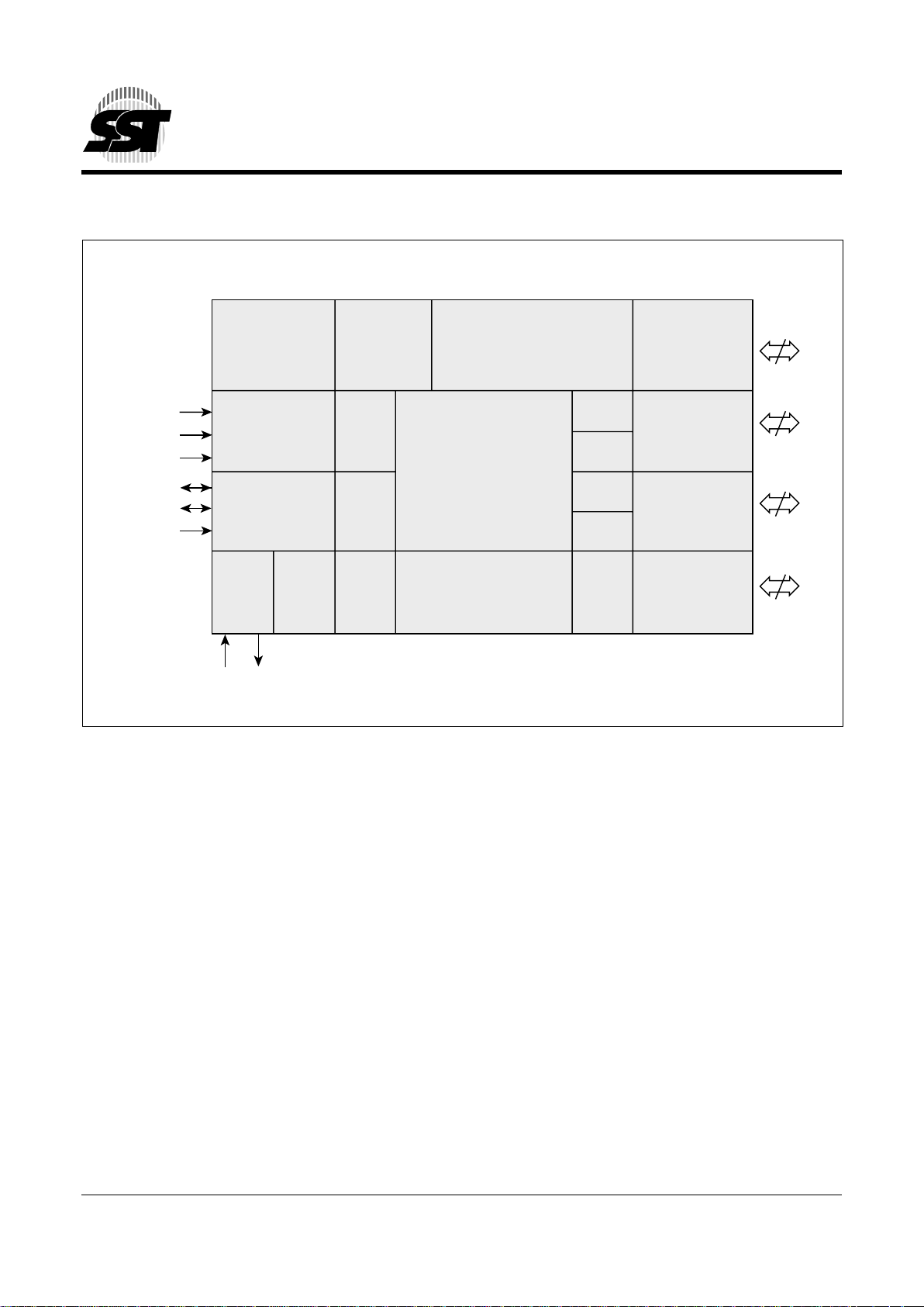
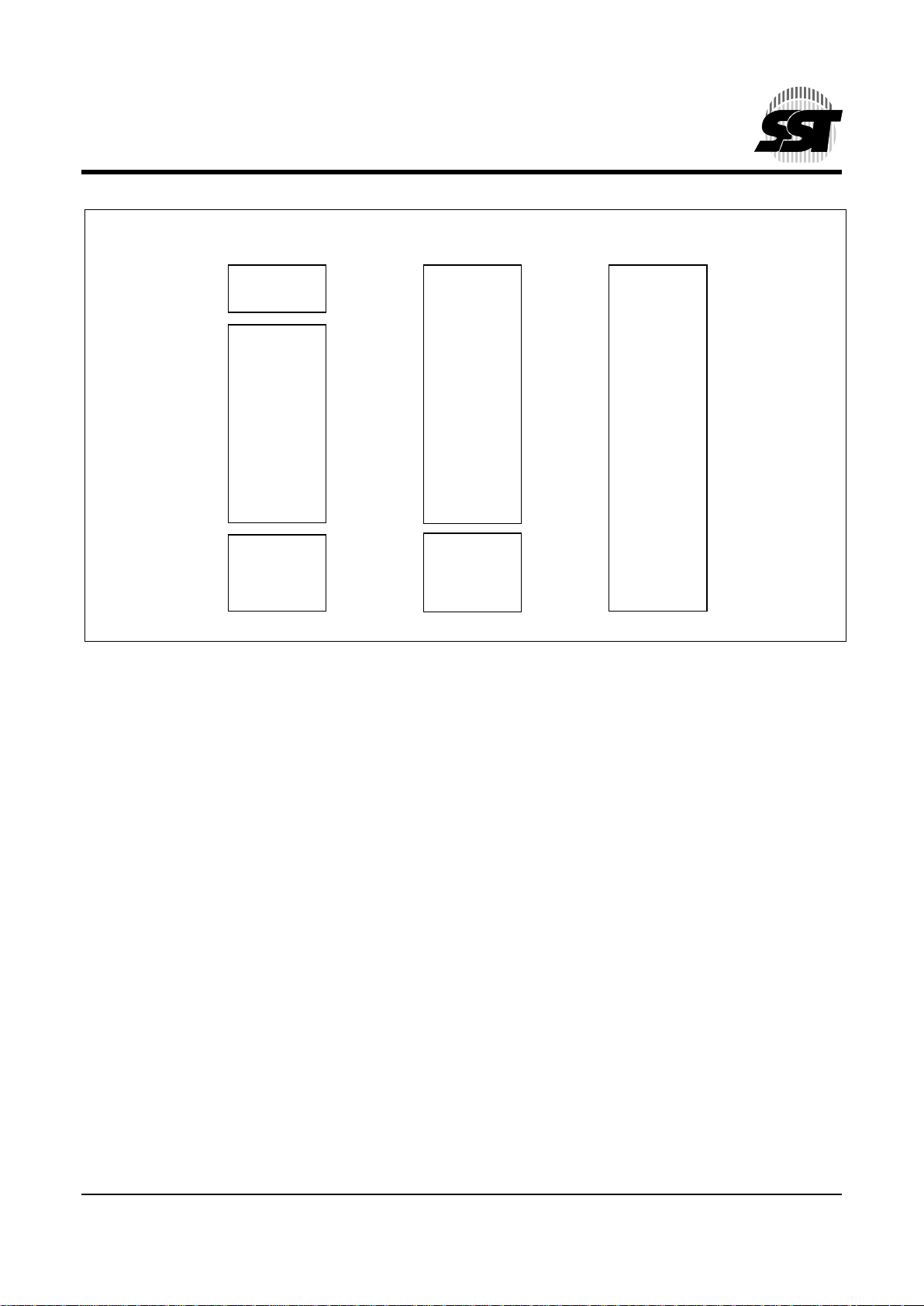
F
UNCTIONAL BLOCK DIAGRAM
FUNCTIONAL BLOCKS
RST
V
SS
V
DD
ALE/PROG#
PSEN#
EA#
XTAL1 XTAL2
SuperFlash
EEPROM
4K x 8
Program/Erase
& IAP
Control
SuperFlash EEPROM
16/32K x 8
CPU
Port 0
8
I/O
8
I/O
8
I/O
8
I/O
Port 1
Power Mode
Management
Bus Controller
T0
T1
T2
WDT
8-bit
UART
RAM
256 x 8
Interrupt
Control
SFRs
Security
Lock
Mode
Control
Oscillator
&
Timing
Port 2
Port 3
344 ILL B1.1
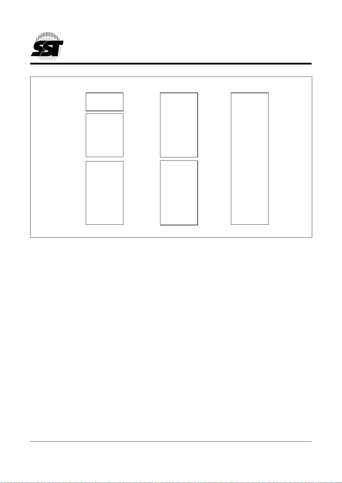
Page 5
5
© 2000 Silicon Storage Technology, Inc. 344-2 8/00
FlashFlex51 MCU
SST89C54 / SST89C58
Preliminary Specifications
1
2
3
4
5
6
7
8
9
10
11
12
13
14
15
16
39
38
37
36
35
34
33
32
31
30
29
7
8
9
10
11
12
13
14
15
16
17
P1.5
P1.6
P1.7
RST
(RXD) P3.0
NC
(TXD) P3.1
(INT0#) P3.2
(INT1#) P3.3
(T0) P3.4
(T1) P3.5
P0.4 (AD4)
P0.5 (AD5)
P0.6 (AD6)
P0.7 (AD7)
EA#
NC
ALE/PROG#
PSEN#
P2.7 (A15)
P2.6 (A14)
P2.5 (A13)
6 5 4 3 2 1 44 43 42 41 40
18 19 20 21 22 23 24 25 26 27 28
P1.4
P1.3
P1.2
P1.1 (T2 Ex)
P1.0 (T2)NCVDDP0.0 (AD0)
P0.1 (AD1)
P0.2 (AD2)
P0.3 (AD3)
(WR#) P3.6
(RD#) P3.7
XTAL2
XTAL1
V
SS
NC
(A8) P2.0
(A9) P2.1
(A10) P2.2
(A11) P2.3
(A12) P2.4
44-Pin PLCC
T op Vie w
344 ILL F20.1
PIN ASSIGNMENTS
FIGURE 1: PIN ASSIGNMENTS FOR 40-PIN PLASTIC DIP
PI-PACKAGE
FIGURE 2: PIN ASSIGNMENTS FOR 44-PIN TQFP
TQJ-PACKAGE
Note: NC pins must be left unconnected.
FIGURE 3: PIN ASSIGNMENTS FOR 44-PIN PLCC
NJ-PACKAGE
40
39
38
37
36
35
34
33
32
31
30
29
28
27
26
25
24
23
22
21
(T2) P1.0
(T2 Ex) P1.1
P1.2
P1.3
P1.4
P1.5
P1.6
P1.7
RST
(RXD) P3.0
(TXD) P3.1
(INT0#) P3.2
(INT1#) P3.3
(T0) P3.4
(T1) P3.5
(WR#) P3.6
(RD#) P3.7
XTAL2
XTAL1
V
SS
1
2
3
4
5
6
7
8
9
10
11
12
13
14
15
16
17
18
19
20
V
DD
P0.0 (AD0)
P0.1 (AD1)
P0.2 (AD2)
P0.3 (AD3)
P0.4 (AD4)
P0.5 (AD5)
P0.6 (AD6)
P0.7 (AD7)
EA#
ALE/PROG#
PSEN#
P2.7 (A15)
P2.6 (A14)
P2.5 (A13)
P2.4 (A12)
P2.3 (A11)
P2.2 (A10)
P2.1 (A9)
P2.0 (A8)
40-Pin PDIP
T op View
344 ILL F18.1
33
32
31
30
29
28
27
26
25
24
23
12 13 14 15 16 17 18 19 20 21 22
1
2
3
4
5
6
7
8
9
10
11
P1.5
P1.6
P1.7
RST
(RXD) P3.0
NC
(TXD) P3.1
(INT0#) P3.2
(INT1#) P3.3
(T0) P3.4
(T1) P3.5
P0.4 (AD4)
P0.5 (AD5)
P0.6 (AD6)
P0.7 (AD7)
EA#
NC
ALE/PROG#
PSEN#
P2.7 (A15)
P2.6 (A14)
P2.5 (A13)
44 43 42 41 40 39 38 37 36 35 34
P1.4
P1.3
P1.2
P1.1 (T2 Ex)
P1.0 (T2)NCVDDP0.0 (AD0)
P0.1 (AD1)
P0.2 (AD2)
P0.3 (AD3)
(WR#) P3.6
(RD#) P3.7
XTAL2
XTAL1
V
SS
NC
(A8) P2.0
(A9) P2.1
(A10) P2.2
(A11) P2.3
(A12) P2.4
44-Pin TQFP
T op Vie w
344 ILL F19.1
Page 6
6
© 2000 Silicon Storage Technology, Inc. 344-2 8/00
FlashFlex51 MCU
SST89C54 / SST89C58
Preliminary Specifications
TABLE 1: PIN DESCRIPTIONS
Symbol Type
1
Name and Functions
P0[7:0] I/O
1
Port 0: Port 0 is an 8-bit open drain bi-directional I/O port. As an output port each
pin can sink several LS TTL inputs. Port 0 pins that have 1’s written to them
float, and in that state can be used as high-impedance inputs. Port 0 is also the
multiplexed low-order address and data bus during accesses to external
memory. In this application it uses strong internal pull-ups when transitioning
to 1’s. Port 0 also receives the code bytes during FLASH MEMORY
programming, and outputs the code bytes during program verification. External
pull-ups are required during program verification.
P1[7:0] I/O with internal Port 1: Port 1 is an 8-bit bi-directional I/O port with internal pull-ups. The Port 1
pull-ups output buffers can drive LS TTL inputs. Port 1 pins that have 1’s written to them
are pulled high by the internal pull-ups, and in that state can be used as
inputs. As inputs, Port 1 pins that are externally pulled low will source current
(I
IL
, on the data sheet) because of the internal pull-ups. P1(5, 6, 7) have high
current drive of 16mA. Port 1 also receives the low-order address bytes during
FLASH MEMORY programming and program verification.
P1[0] I T2: (external count input to Timer/Counter 2), clock-out
P1[1] I T2EX: (Timer/Counter 2 capture/reload trigger and direction control)
P2[7:0] I/O with internal Port 2: Port 2 is an 8-bit bi-directional I/O port with internal pull-ups. Port 2 pins
pull-ups that have 1’s written to them are pulled high by the internal pull-ups, and
in that state can be used as inputs. As inputs, Port 2 pins that are externally
pulled low will source current (IIL, on the data sheet) because of the internal
pull-ups. Port 2 sends the high-order address byte during fetches from external
Program memory and during accesses to external Data Memory that use 16-bit
address (MOVX@DPTR). In this application it uses strong internal pull-ups
when outputting 1’s. During accesses to external Data Memory that use 8-bit
addresses (MOVX@Ri), Port 2 sends the contents of the P2 Special Function
Register. Port 2 also receives some control signals and a partial of high-order
address bits during FLASH MEMORY programming and program verification.
P3[7:0] I/O with internal Port 3: Port 3 is an 8-bit bidirectional I/O port with internal pull-ups. The Port 3
pull-ups output buffers could drive LS TTL inputs. Port 3 pins that have 1’s written to them
are pulled high by the internal pull-ups, and in that state can be used as inputs.
As inputs, Port 3 pins that are externally pulled low will source current (IIL, on the
data sheet) because of the pull-ups. Port 3 also serves the functions of various
special features of the FlashFlex51 Family. Port 3 also receives some control
signals and a partial of high-order address bits during FLASH MEMORY
programming and program verification.
P3[0] I RXD: Serial input line
P3[1] O TXD: Serial output line
P3[2] I INT0#: External Interrupt 0
P3[3] I INT1#: External Interrupt 1
P3[4] I T0: Timer 0 external input
P3[5] I T1: Timer 1 external input
P3[6] O WR#: External Data Memory Write strobe
P3[7] O RD#: External Data Memory Read strobe
Page 7

7
© 2000 Silicon Storage Technology, Inc. 344-2 8/00
FlashFlex51 MCU
SST89C54 / SST89C58
Preliminary Specifications
1
2
3
4
5
6
7
8
9
10
11
12
13
14
15
16
PIN DESCRIPTIONS (CONTINUED)
Symbol Type
1
Name and Functions
PSEN# O/I Program Store Enable: PSEN# is the Read strobe to External Program
Memory. When the SST89C54/58 are executing from Internal Program
Memory, PSEN# is inactive (high). When the device is executing code from
External Program Memory, PSEN# is activated twice each machine cycle,
except that two PSEN# activations are skipped during each access to External
Data Memory. While the RST input is continually held high (for more than ten
machine cycles), a forced high-to-low input transition on the PSEN# pin will bring
the device into the “External Host” mode for the internal flash memory
programming operation.
RST I Reset: A high logic state on this pin for two machine cycles (at least 24 oscillator
periods), while the oscillator is running resets the device. After a successful reset
is completed, if the PSEN# pin is driven by an input force with a high-to-low
transition while the RST input pin is continually held high, the device will enter the
“External Host” mode for the internal flash memory programming operation,
otherwise the device will enter the “Normal” operation mode.
EA# I External Access Enable: EA# must be connected to VSS in order to enable the
SST89C54/58 to fetch code from External Program Memory locations starting
at 0000h up to FFFFh. Note, however, that if the Security Lock is activated on
either block, the logic level at EA# is internally latched during reset. EA# must be
connected to VDD for internal program execution. The EA# pin can tolerate a high
voltage2 of 12V (see Electrical Specification).
ALE/PROG# I/O Address Latch Enable: ALE is the output signal for latching the low byte of the
address during accesses to external memory. This pin is also the programming
pulse input (PROG#).
XTAL1 I Oscillator: Input and output to the inverting oscillator amplifier. XTAL1 is input to
XTAL2 O internal clock generation circuits from an external clock source.
V
DD
I Power Supply: Supply voltage during normal, Idle, Power Down, and Standby
Mode operations.
Vss I Ground: Circuit ground. (0V reference)
344 PGM T1.6
Note: 1) I = Input
O = Output
2) It is not necessary to receive a 12V programming supply voltage during flash programming.
Page 8
8
© 2000 Silicon Storage Technology, Inc. 344-2 8/00
FlashFlex51 MCU
SST89C54 / SST89C58
Preliminary Specifications
MEMORY ORGANIZATION
The SST89C54/58 have separate address spaces for
program and data memory.
Program Memory
There are two internal flash memory blocks in the
SST89C54/58. The primary flash memory Block 0 has
16/32 KByte and occupies the address space 0000h to
3FFFh/7FFFh. The secondary flash memory Block 1 has
4 KByte and occupies the address space F000h to
FFFFh.
The 16/32K x8 primary SuperFlash block is organized as
128/256 uniform sectors with sector address from A15 to
A7. Each sector contains 2 rows with row address from
A15 to A6. Each row has 64 Bytes with byte address from
A5 to A0.
F
IGURE 4: SECTOR ORGANIZATION
The 4K x8 secondary SuperFlash block is organized as
64 uniform sectors with sector address from A15 to A6.
Each sector contains 2 rows with row address from A15
to A5. Each row contains 32 Bytes with byte address
from A4 to A0. Figure 4 shows the sector organization for
SST89C54/58.
When internal code operation is enabled (EA# = 1), the
primary 16/32 KByte flash memory block is always
visible to the program counter for code fetching. Figures
5 and 6 show the program memory organizations for the
SST89C54/58.
When internal code operation is enabled (EA# = 1), the
secondary 4 KByte flash memory block is selectively
visible for code fetching. The secondary block is always
accessible through the SuperFlash mailbox registers:
SFCM, SFCF, SFAL, SFAH, SFDT and SFST. When bit
7 of the SuperFlash Configuration mailbox register
(SFCF[7]), SFR address location B1h, is set, the secondary 4 KByte block will be visible by program counter.
7FFFh
7F80h
4000h
3FFFh
0000h
Block 0 (16/32 KByte)
344 ILL F47.6
Sector 255
Sector 127
Sector 0
3F80h
007Fh
FFFFh
FFC0h
F03Fh
Block 1 (4 KByte)
Primary Secondary
Sector 63
Sector 0
F000h
89C58
89C54
Page 9
9
© 2000 Silicon Storage Technology, Inc. 344-2 8/00
FlashFlex51 MCU
SST89C54 / SST89C58
Preliminary Specifications
1
2
3
4
5
6
7
8
9
10
11
12
13
14
15
16
FIGURE 5: SST89C54 PROGRAM MEMORY ORGANIZATION
344 ILL F21.1
48 KByte
EXTERNAL
64 KByte
EXTERNAL
16 KByte
INTERNAL
(Block 0)
44 KByte
EXTERNAL
16 KByte
INTERNAL
(Block 0)
4 KByte
INTERNAL
(Block 1)
EA# = 1 & SFCF[7] = 1 EA# = 1 & SFCF[7] = 0 EA# = 0
FFFFh
EFFFh
F000h
4000h
0000h
3FFFh
FFFFh
4000h
0000h
FFFFh
0000h
3FFFh
Page 10
10
© 2000 Silicon Storage Technology, Inc. 344-2 8/00
FlashFlex51 MCU
SST89C54 / SST89C58
Preliminary Specifications
Memory Re-mapping
The SST89C54/58 memory re-mapping feature allows
users to reorganize internal Flash memory sectors so
that interrupts may be serviced when Block 0 of the
internal Flash is being programmed. Since Block 0
occupies the low order program address space of the
8051 architecture where the interrupt vectors reside,
those interrupt vectors will normally not be available
when Block 0 is being programmed.
SST89C54/58 provides four options of Memory Remapping (Refer to Table 2). When the lowest 4 KBytes
are remapped, any program access within logical address range 0000h – 0FFFh will have the 4 most significant address bits forced to “1”, redirecting the access to
F000h – FFFFh. Note that the physical contents of the
re-mapped portion of Block 0 (i.e. physical locations
0000h – 0FFFh in the current example) will not be
accessible. Block 1 will still also be accessible through
F000h – FFFFh. Figures 7 and 8 show re-mapped
program memory organization for the SST89C54/58.
FIGURE 6: SST89C58 PROGRAM MEMORY ORGANIZATION
344 ILL F11.1
32 KByte
EXTERNAL
64 KByte
EXTERNAL
32 KByte
INTERNAL
(Block 0)
28 KByte
EXTERNAL
32 KByte
INTERNAL
(Block 0)
4 KByte
INTERNAL
(Block 1)
EA# = 1 & SFCF[7] = 1 EA# = 1 & SFCF[7] = 0 EA# = 0
FFFFh
EFFFh
F000h
8000h
0000h
7FFFh
FFFFh
8000h
0000h
FFFFh
0000h
7FFFh
Page 11

11
© 2000 Silicon Storage Technology, Inc. 344-2 8/00
FlashFlex51 MCU
SST89C54 / SST89C58
Preliminary Specifications
1
2
3
4
5
6
7
8
9
10
11
12
13
14
15
16
Activation and Deactivation of Memory Re-mapping
The actual amount of memory that is re-mapped is
controlled by MAP_EN[1:0] bits as shown in Table 2. The
MAP_EN[1:0] bits are the same bits as SFCF[1:0]. The
MAP_EN[1:0] bits are under software control and can be
changed during program execution. Since changing re-
mapping will cause program re-location, it is advisable
that the instruction that changes the MAP_EN[1:0] be in
the portion of memory that is not affected by the remapping change.
The MAP_EN[1:0] bits are initialized at Reset according
to the contents of two non-volatile register bits, ReMap[1:0] (as shown in Table 2). The Re-Map[1:0] bits are
programmed via PROG_RB1 and PROG_RB0 External
Host Mode commands. Refer to External Host Program-
ming Mode section for PROG_RB1 and PROG_RB0
commands.
The contents of MAP_EN[1:0] are only updated according to Re-Map[1:0] on a successful reset. Any subsequent alteration to the Re-Map[1:0] bits will not automatically change the MAP_EN[1:0] bits without a reset.
Similarly, changes to MAP_EN[1:0] during program execution will not change Re-Map[1:0] bits.
To deactivate memory re-mapping, a CHIP-ERASE operation will revert Re-Map[1:0] to the default status of
“11”, disabling re-mapping. Programming 00b to
SFCF[1:0] register also deactivates memory re-mapping. The effect of programming Re-Map[1:0] is available
only after the next reset. Refer to In-Application Mode
Commands section for more detailed information.
TABLE 2: RE-MAPPING TABLE
Re-Map [1:0]
1
MAP_EN
2,3
Comments
11 00 Re-mapping is turned off. Program memory is in normal
configuration.
10 01 1 KByte of flash memory location is re-mapped. Program access
to location 0000h-03FFh is redirected to F000h – F3FFh.
01 10 2 KBytes of flash memory location are re-mapped. Program access
to location 0000h-07FFh is redirected to F000h – F7FFh.
00 11 4 KBytes of flash memory location is re-mapped. Program access
to location 0000h-0FFFh is redirected to F000h – FFFFh.
1 Re-Map[1:0] are nonvolatile registers which are examined only during Reset.
2 MAP_EN[1:0] are initialized according to Re-Map[1:0] during Reset.
3 MAP_EN[1:0] are located in SFCF[1:0], they determine the Re-Mapping configuration. They may be changed by the program at run time.
344 PGM T2.3
Page 12
12
© 2000 Silicon Storage Technology, Inc. 344-2 8/00
FlashFlex51 MCU
SST89C54 / SST89C58
Preliminary Specifications
F
IGURE 7: SST89C54 RE-MAPPED PROGRAM MEMORY ORGANIZATION
FIGURE 8: SST89C58 RE-MAPPED PROGRAM MEMORY ORGANIZATION
28 KByte
EXTERNAL
31/30/28
KByte
INTERNAL
(Block 0)
1/2/4 KByte
INTERNAL
(Block 1)
4 KByte
INTERNAL
(Block 1)
EA# = 1 & SFCF[7] = 1
SFCF [1:0] = 01/10/11
FFFFh
EFFFh
F000h
7FFFh
8000h
7FFFh
8000h
0000h
32 KByte
EXTERNAL
31/30/28
KByte
INTERNAL
(Block 0)
1/2/4 KByte
INTERNAL
(Block 1)
344 ILL F36.1
EA# = 1 & SFCF[7] = 0
SFCF [1:0] = 01/10/11
FFFFh
0000h
44 KByte
EXTERNAL
15/14/12
KByte
INTERNAL
(Block 0)
1/2/4 KByte
INTERNAL
(Block 1)
4 KByte
INTERNAL
(Block 1)
EA# = 1 & SFCF[7] = 1
SFCF [1:0] = 01/10/11
FFFFh
EFFFh
F000h
3FFFh
4000h
3FFFh
4000h
0000h
48 KByte
EXTERNAL
15/14/12
KByte
INTERNAL
(Block 0)
1/2/4 KByte
INTERNAL
(Block 1)
344 ILL F35.3
EA# = 1 & SFCF[7] = 0
SFCF [1:0] = 01/10/11
FFFFh
0000h
Page 13
13
© 2000 Silicon Storage Technology, Inc. 344-2 8/00
FlashFlex51 MCU
SST89C54 / SST89C58
Preliminary Specifications
1
2
3
4
5
6
7
8
9
10
11
12
13
14
15
16
Data Memory
SST89C54/58 have 256 x 8 bits of on-chip RAM and can address up to 64 KBytes of external data memory.
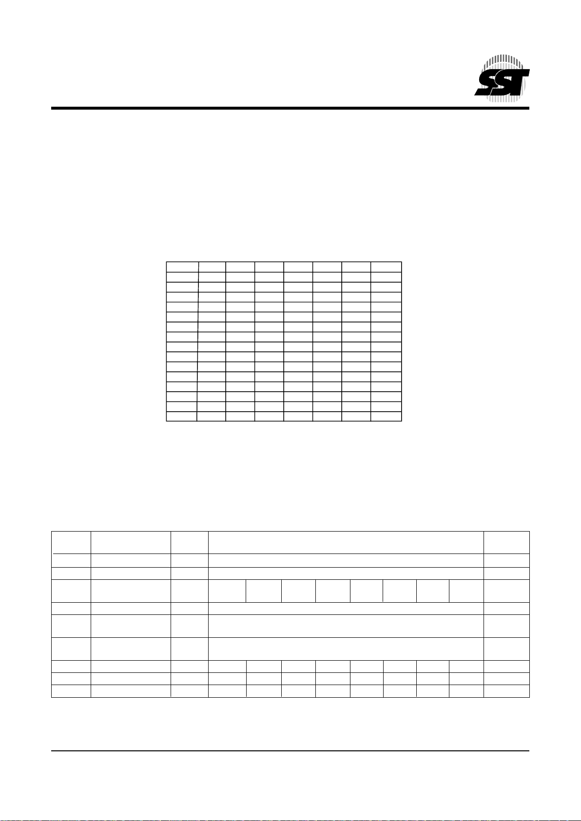
Special Function Registers (SFR)
Most of the unique features of the FlashFlex51 microcontroller family are controlled by bits in special function registers
(SFRs) located in the FlashFlex51 SFR Memory Map shown below. Individual descriptions of each SFR are provided
and Reset values indicated in Tables 3
A to 3E.
F8
F0
E8
E0
D8
D0
C8
C0
B8
B0
A8
A0
98
90
88
80
FF
F7
EF
E7
DF
D7
CF
C7
BF
B7
AF
A7
9F
97
8F
87
B*
ACC*
PSW*
T2CON*
RCAP2L
RCAP2H
TL2 TH2
WDTC*
IP*
P3* SFCF SFCM SFAL SFAH SFDT SFST
IE*
P2*
SCON*
SBUF
P1*
TCON* TMOD TL0 TL1 TH0 TH1
P0* SP DPL DPH WDTD PCON
8 BYTES
FlashFlex51 SFR Memory Map
* = Bit Addressable SFRs
All addresses are hexadecimal
344 ILL F23.1
SST89C54/58 Special Function Registers
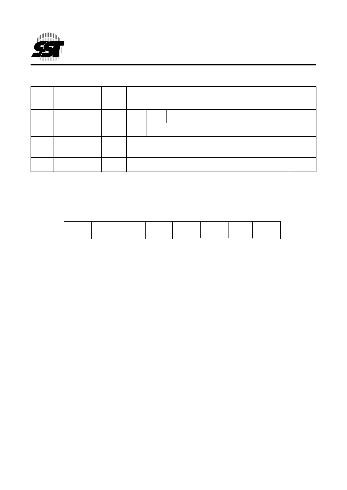
TABLE 3A: CPU RELATED SFRS
Symbol Description Direct Bit Address, Symbol, or Alternative Port Function RESET
Address MSB LSBValue
ACC* Accumulator E0h ACC[7:0] 00h
B* B Register F0h B[7:0] 00h
PSW* Program Status D0h CY AC F0 RS1 RS0 OV F1 P 0 0h
Word
SP Stack Pointer 81h SP[7:0] 07h
DPL Data Pointer 82h DPL[7:0] 00h
Low 0
DPH Data Pointer 83h DPH[7:0] 00h
High 0
IE* Interrupt Enable A8h EA - ET2 ES0 ET1 EX1 ET0 EX0 40h
IP* Interrupt Priority B8h - - PT2 PS PT1 PX1 PT0 PX0 xx000000b
PCON Power Control 87h SMOD - - - GF1 GF0 PD IDL 0xxx0000b
* = Bit Addressable SFRs
344 PGM T3A.3
Page 14
14
© 2000 Silicon Storage Technology, Inc. 344-2 8/00
FlashFlex51 MCU
SST89C54 / SST89C58
Preliminary Specifications
SuperFlash Status Register (SFST) (Read Only Register)
Location 76543210Reset Value
0B6h SECD2 SECD1 SECD0 – Busy Flash_busy ––xxx00000b
Symbol Function
SECD2 Security bit 1.
SECD1 Security bit 2.
SECD0 Security bit 3.
Please refer to Table 8 for security lock options.
BUSY Burst-Program completion polling bit.
1: Device is busy with flash operation.
0: Device is available for next Burst-Program operation.
Flash_busy Flash operation completion polling bit.
1: Device is busy with flash operation.
0: Device has fully completed the last command, including Burst-Program.
TABLE 3B: FLASH MEMORY PROGRAMMING SFRS
Symbol Description Direct Bit Address, Symbol, or Alternative Port Function RESET
Address MSB LSB Value
SFST SuperFlash Status B6h SECD[2:0] - BUSY
Flash_busy
- - xxx00000b
SFCF SuperFlash B1h VIS IAPEN - - - - MAP_EN 000000xxb
Configuration
SFCM SuperFlash B2h FIE FCM 00h
Command
SFDT SuperFlash Data B5h SuperFlash Data Register 00h
SFAL SuperFlash B3h SuperFlash Low Order Byte Address Register – A7 to A0 (SFAL) 00h
Address Low
SFAH SuperFlash B4h SuperFlash High Order Byte Address Register – A15 to A8 (SFAH) 00h
Address High
344 PGM T3B.4
Page 15
15
© 2000 Silicon Storage Technology, Inc. 344-2 8/00
FlashFlex51 MCU
SST89C54 / SST89C58
Preliminary Specifications
1
2
3
4
5
6
7
8
9
10
11
12
13
14
15
16
SuperFlash Configuration Register (SFCF)
Location 76543210Reset Value
0B1h VIS IAPEN ––––
MAP_EN1 MAP_EN0
000000xxb
Symbol Function
VIS Upper flash block visibility.
1: 4 KByte flash block visible from F000-FFFF.
0: 4 KByte flash block not visible.
IAPEN Enable IAP operation.
1: IAP commands are enabled.
0: IAP commands are disabled.
MAP_EN1 Map enable bit 1.
MAP_EN0 Map enable bit 0.
MAP_EN[1:0] are initialized to default value according to Re-map [1:0] during Reset.
Refer to Table 2.
SuperFlash Command Register (SFCM)
Location 76543210Reset Value
0B2h FIE FCM6 FCM5 FCM4 FCM3 FCM2 FCM1 FCM0 00000000b
Symbol Function
FIE Flash Interrupt Enable.
1: INT1# is re-assigned to signal IAP operation completion.
External INT1# interrupts are ignored.
0: INT1# is not reassigned.
FCM[6:0] Flash operation command.
000_0001b Chip-Erase.
000_0110b Burst-Program.
000_1011b Sector-Erase.
000_1100b Byte-Verify.
(1)
000_1101b Block-Erase.
000_1110b Byte-Program.
All other combinations are not implemented, and reserved for future use.
(1)
Byte-Verify has a single machine cycle latency and will not generate any INT1# interrupt regardless of FIE.
Page 16

16
© 2000 Silicon Storage Technology, Inc. 344-2 8/00
FlashFlex51 MCU
SST89C54 / SST89C58
Preliminary Specifications
SuperFlash Data Register (SFDT)
Location 7 6 543210Reset Value
0B5h SuperFlash Data Register 00000000b
Symbol Function
SFDT Mailbox register for interfacing with flash memory block (Data register).
SuperFlash Address Registers (SFAL)
Location 7 6 543210Reset Value
0B3h SuperFlash Low Order Byte Address Register 00000000b
Symbol Function
SFAL Mailbox register for interfacing with flash memory block. (Low order address register).
SuperFlash Address Registers (SFAH)
Location 7 6 543210Reset Value
0B4h SuperFlash High Order Byte Address Register 00000000b
Symbol Function
SFAH Mailbox register for interfacing with flash memory block. (High order address register).
Page 17

17
© 2000 Silicon Storage Technology, Inc. 344-2 8/00
FlashFlex51 MCU
SST89C54 / SST89C58
Preliminary Specifications
1
2
3
4
5
6
7
8
9
10
11
12
13
14
15
16
Watchdog Timer Control Register (WDTC)
Location 76543210Reset Value
0C0h –
––– WDRE WDTS WDT SWDT 00000000b
Symbol Function
WDRE Watchdog timer reset enable.
1: Enable watchdog timer reset.
2: Disable watchdog timer reset.
WDTS Watchdog timer reset flag.
1: Hardware sets the flag on watchdog overflow.
0: External hardware reset clears the flag.
Flag can also be cleared by writing a 1.
Flag survives if chip reset happened because of watchdog timer overflow.
WDT Watchdog timer refresh.
1: Software sets the bit to force a watchdog timer refresh.
0: Hardware resets the bit when refresh is done.
SWDT Start watchdog timer.
1: Start WDT.
0: Stop WDT.
Watchdog Timer Data/Reload Register (WDTD)
Location 76543210Reset Value
086h Watchdog Timer Data/Reload 00000000b
Symbol Function
WDTD Initial/Reload value in Watchdog Timer.
TABLE 3C: WATCHDOG TIMER SFRS
WDTC* Watchdog Timer C0h -
--
- WDRE WDTS WDT SWDT X0h
Control
WDTD Watchdog Timer 86h WDRL 00h
Data/Reload
* = Bit Addressable SFRs
344 PGM T3C.1
Page 18

18
© 2000 Silicon Storage Technology, Inc. 344-2 8/00
FlashFlex51 MCU
SST89C54 / SST89C58
Preliminary Specifications
FLASH MEMORY PROGRAMMING
The SST89C54/58 internal flash memory can be programmed or erased using the following two methods:
• External Host Mode (parallel only)
• In-Application Programming (IAP) Mode
(parallel or serial)
EXTERNAL HOST PROGRAMMING MODE
External Host Programming Mode provides the user with
direct Flash memory access to program the Flash
memory without using the CPU. External Host Mode is
entered by forcing PSEN# from a logic high to a logic low
while RST input is being held continuously high. The
SST89C54/58 will stay in External Host Mode as long as
RST = 1 and PSEN# = 0.
A READ-ID operation is necessary to “arm” the device,
no other External Host Mode command can be enabled
until a READ-ID is performed. In External Host Mode, the
internal Flash memory blocks are accessed through the
re-assigned I/O port pins (see Figure 9 for details) by an
external host, such as an MCU programmer, PCB tester
or a PC controlled development board.
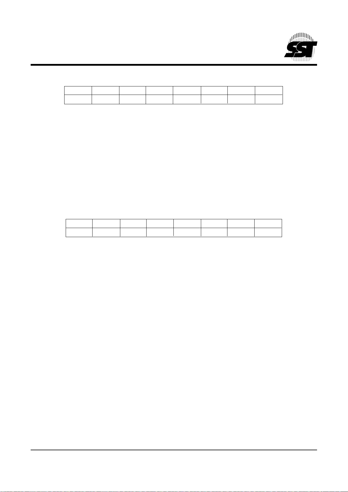
TABLE 3D: TIMER/COUNTERS SFRS
TMOD Timer/Counter 89h Timer 1 Timer 0 00h
Mode Control GATE C/T# M1 M0 GATE C/T# M1 M0
TCON* Timer/Counter 88h TF1 TR1 TF0 TR0 IE1 IT1 IE0 IT0 00h
Control
TH0 Timer 0 MSB 8Ch TH0[7:0] 00h
TL0 Timer 0 LSB 8Ah TL0[7:0] 00h
TH1 Timer 1 MSB 8Dh TH1[7:0] 00h
TL1 Timer 1 LSB 8Bh TL1[7:0] 00h
T2CON* Timer / Counter 2 C8h TF2 EXF2 RCLK TCLK EXEN2 TR2 C/T2# CP/RL2# 00h
Control
TH2 Timer 2 MSB CDh TH2[7:0] 00h
TL2 Timer 2 LSB CCh TL2[7:0] 00h
RCAP2H Timer 2 Capture MSB
CBh RCAP2H[7:0] 00h
RCAP2L Timer 2 Capture LSB
CAh RCAP2L[7:0] 00h
* = Bit Addressable SFRs
344 PGM T3D.0
TABLE 3E: INTERFACE SFRS
SBUF Serial Data Buffer 99h SBUF[7:0] Indeterminate
SCON* Serial Port Control 98h SM0 SM1 SM2 REN TB8 RB8 T1 R1 00h
P0* Port 0 80h P0[7:0] FFh
P1* Port 1 90h - ---- T2 EXT2FFh
P2* Port 2 A0h P2[7:0] FFh
P3* Port 3 B0h RD# WR# T1 T0 INT1# INT0# TXD0 RXD0 FFh
* = Bit Addressable SFRs
344 PGM T3E.3
Page 19

19
© 2000 Silicon Storage Technology, Inc. 344-2 8/00
FlashFlex51 MCU
SST89C54 / SST89C58
Preliminary Specifications
1
2
3
4
5
6
7
8
9
10
11
12
13
14
15
16
Operation RST PSEN# PROG# EA# P3[7] P3[6] P2[7] P2[6] P0[7:0] P1[7:0] P3[5:4]
/ALE P2[5:0]
READ-ID H L H H L L L L DO AL AH
CHIP-ERASE H L
ß
HLL LH X X X
BLOCK-ERASE H L
ß
H H H L H X X A[15:12]
SECTOR-ERASE H L
ß
HHL HH X AL AH
BYTE-PROGRAM H L
ß
HHH HL DI AL AH
BURST-PROGRAM H L
ß
HLH HL DI AL AH
BYTE-VERIFY H L H H H H L L DO AL AH
(Read)
PROG-SB1 H L
ß
HHH HH X X X
PROG-SB2 H L
ß
HLL HH X X X
PROG-SB3 H L
ß
HLH LH X X X
PROG-RB0 H L
ß
HHL LL X X X
PROG-RB1 H L
ß
HHL LH X X X
Note: Symbol ß signifies a negative pulse and the command is asserted during the low state of PROG#/ALE input. All other
combinations of the above input pins are invalid and may result in unexpected behaviors.
Note: L = Logic low level; H = Logic high level; X = Don‘t care; AL = Address low order byte; AH = Address high order byte;
DI = Data Input; DO = Data Output; A[15:12] = 0xxxb for Block 0 and A[15:12} = “Fh” for Block 1.
TABLE 4: EXTERNAL HOST MODE COMMANDS
344 PGM T4.4
When the chip is in the External Host Mode, Port 0 pins
are assigned to be the parallel data input and output pins.
Port 1 pins are assigned to be the non-multiplexed low
order address bus signals for the internal flash memory
(A7-A0). The first six bits of Port 2 pins (P2[5:0]) are
assigned to be the non-multiplexed upper order address
bus signals for the internal flash memory (A13-A8) along
with two of the Port 3 pins (P3[5] as A15 and P3[4] as
A14). Two upper order Port 2 pins (P2[7] and P2[6]) and
two upper order Port 3 pins (P3[7] and P3[6]) along with
RST, PSEN#, PROG#/ALE, EA# pins are assigned as
the control signal pins. The Port 3 pin (P3[3]) is assigned
to be the ready/busy status signal, which can be used for
handshaking with the external host during a flash
memory programming operation. The flash memory
programming operation (Erase, Program, Verify, etc.) is
internally self-timed.
The insertion of an “arming” command prior to entering
the External Host Mode by utilizing the “READ-ID” operation provides additional protection for inadvertent
writes to the internal flash memory caused by a noisy or
unstable system environment during power-up or brownout conditions.
The External Host Mode uses twelve (12) hardware
commands, which are decoded from the control signal
pins, to facilitate the internal flash memory erase, program and verify processes. The External Host Mode is
enabled on the falling edge of PSEN#. The External Host
Mode Commands are enabled on the falling edge of ALE/
PROG#. The list in Table 4 outlines all the commands
and the respective control signal assignment.
Page 20

20
© 2000 Silicon Storage Technology, Inc. 344-2 8/00
FlashFlex51 MCU
SST89C54 / SST89C58
Preliminary Specifications
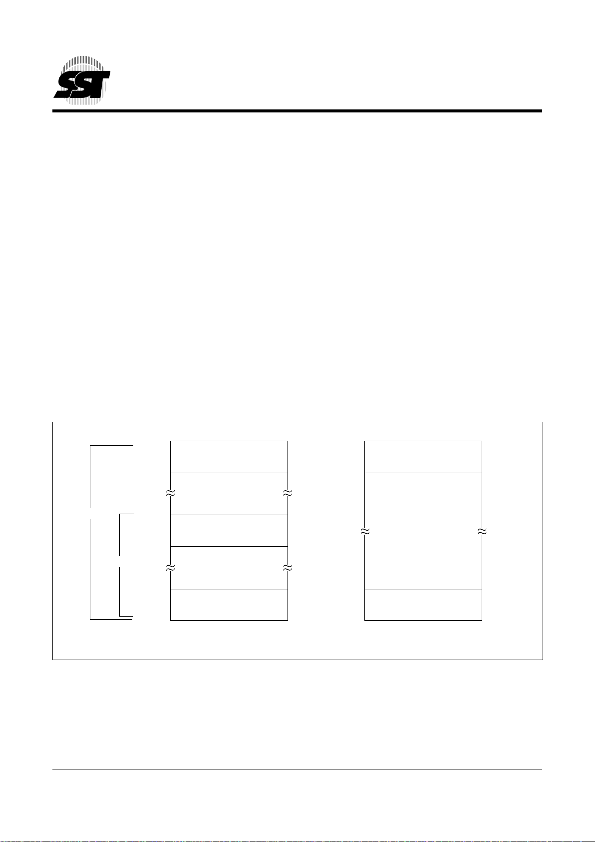
F
IGURE 9: I/O PIN ASSIGNMENTS FOR EXTERNAL HOST MODE
Product Identification
The READ-ID command accesses the Signature Bytes
that identifies the device as an SST89C54/58 and the
manufacturer as SST. External programmers primarily
use these Signature Bytes, shown in Table 5, in the
selection of programming algorithms. The Read-ID command is selected by the byte code of 00h on
P2[7:6] and P3[7:6]. See Figure 10 for timing waveforms.
External Host Mode Commands
The twelve SST89C54/58 External Host Mode Commands are READ-ID, CHIP-ERASE, BLOCK-ERASE
SECTOR-ERASE, BYTE-PROGRAM, BURST-PROGRAM, BYTE-VERIFY, PROG-SB1, PROG-SB2,
PROG-SB3, PROG-RB0 and PROG-RB1. See Table 4
for all signal logic assignments and Table 7 for all timing
parameter values for the External Host Mode Commands. The critical timing for all Erase and Program
commands, is self-generated by the on-chip flash
memory controller. The high-to-low transition of the
PROG# signal initiates the Erase and Program commands, which are synchronized internally. The Read
commands are asynchronous reads, independent of the
PROG# signal level.
The following three commands are used for erasing all or
part of the memory array. All the data in the memory array
will be erased to FFh. Memory locations that are to be
programmed must be in the erased state prior to
programming. Selection of the Erase command to use,
prior to programming the device, will be dependent upon
the contents already in the array and the desired field
size to be programmed.
The CHIP-ERASE command erases all bytes in both
memory blocks (Block 0 and Block 1) of the SST89C54/
58. This command ignores the Security Lock status and
will erase the Security bits and the Re-Map bits. The
CHIP-ERASE command is selected by the binary code
of 00b on P3[7:6] and 01b on P2[7:6]. See Figure 11 for
timing waveforms.
The BLOCK-ERASE command erases all bytes in one of
the memory blocks (16/32K or 4K) of the SST89C54/58.
This command will not be enabled if the security lock is
enabled on the selected memory block. The selection of
the memory block to be erased is determined by A[15:12]
(P3[5], P3[4], P2[5], P1[4]). If A15 is a “0”, then the
primary flash memory Block 0 (16/32K), is selected. If
A[15:12] = “Fh”, then the secondary flash memory Block
1 (4K) is selected. The BLOCK-ERASE command is
selected by the binary code of 11b on P3[7:6] and 01b on
P2[7:6]. See Figure 12 for the timing waveforms.
The SECTOR-ERASE command erases all of the bytes
in a sector. The sector size for the primary flash memory
(Addresses 0000h-3FFFh/7FFFh) is 128 Bytes. The
sector size for the secondary flash memory (Addresses
F000h-FFFFh) is 64 bytes. This command will not be
executed if the Security lock is enabled on the selected
memory block. The selection of the memory sector to be
erased is determined by P1[7:6] (A7 & A6), P2[5:0] (A13A8) and P3[5:4] (A15 & A14). The SECTOR-ERASE
command is selected by the binary code of 10b on
P3[7:6] and 11b on P2[7:6]. See Figure 13 for timing
waveforms.
TABLE 5: SIGNATURE BYTES TABLE
Address Data
Manufacturer’s Code 30h BFh
SST89C54 Device Code 31h E4h
SST89C58 Device Code 31h E2h
344 GPM T5.1
Flash
Control Signals
Address Bus
A7-A0
Flash
Control Signals
Address Bus
A13-A8
Input/
Output
Data
Bus
Port 0
V
SS
XTAL1
XTAL2
Busy/Ready
Port 3
V
DD
RST
Port 2
Port 1
EA# ALE /
PROG#
PSEN#
7
6
5
A15
A14
4
3
2
1
0
7
6
7
6
5
4
3
2
1
0
0
7
6
0
Address Bus
A15-A14
344 ILL F01.1
Page 21

21
© 2000 Silicon Storage Technology, Inc. 344-2 8/00
FlashFlex51 MCU
SST89C54 / SST89C58
Preliminary Specifications
1
2
3
4
5
6
7
8
9
10
11
12
13
14
15
16
The BYTE-PROGRAM and BURST-PROGRAM commands are used for programming new data into the
memory array. Selection of which Program command to
use will be dependent upon the desired programming
field size. Programming will not take place if any security
locks are enabled on the selected memory block.
The BYTE-PROGRAM command programs data into a
single byte. Ports P0[7:0] are used for data in. The
memory location is selected by P1[7:0], P2[5:0], and
P3[5:4] (A15-A0). The BYTE-PROGRAM command is
selected by the binary code of 11b on P3[7:6] and 10b on
P2[7:6]. See Figure 14 for timing waveforms.
The BURST-PROGRAM command programs data to an
entire row, sequentially byte-by-byte. Ports P0[7:0] are
used for data in. The memory location is selected
by P1[7:0], P2[5:0], and P3[5:4] (A15-A0). The BURSTPROGRAM command is selected by the binary code of
01b on P3[7:6] and 10b on P2[7:6]. See Figure 15 for
timing waveforms.
The BYTE-VERIFY command allows the user to verify
that the SST89C54/58 correctly performed an Erase or
Program command. Ports P0[7:0] are used for data out.
The memory location is selected by P1[7:0], P2[5:0], and
P3[5:4] (A15-A0). The BYTE-VERIFY command is selected by the binary code of 11b on P3[7:6] and 00b on
P2[7:6]. This command will be disabled if any security
locks are enabled on the selected memory block. See
Figure 16 for timing waveforms.
The PROG-SB1, PROG-SB2, PROG-SB3 commands
program the security bits, the functions of these bits are
described in a Security Lock section and also in Table 8.
Once programmed, these bits can only be cleared
through a CHIP-ERASE command.
The PROG-RB1, and PROG-RB0 commands program
the Re-Map[1:0] bits. The Re-Map[1:0] bits determine
the Memory Re-mapping default option on reset. Upon
completion of the Reset sequence, the MAP_EN[1:0]
bits are initialized to the default value set by the ReMap[1:0] bits according to Table 2. Subsequent program
manipulation of MAP_EN[1:0] bits will alter the Memory
Re-mapping option but will not change the Re-Map[1:0]
bits. Therefore, any changes to MAP_EN[1:0], without
corresponding updates to Re-Map[1:0], will not survive a
Reset cycle.
If an External Host Mode command, except for CHIPERASE, is issued to a locked memory block, the device
will ignore this command.
External Host Mode Clock Source
In External Host Mode, an internal oscillator will provide
clocking for the SST89C54/58. The on-chip oscillator will
be turned on as the SST89C54/58 enters External Host
Mode; i.e. when PSEN# goes low while RST is high. The
oscillator provides both clocking for the Flash Control
Unit as well as timing references for Program and Erase
operations. During External Host Mode, the CPU core is
held in reset. Upon exit from External Host Mode, the
internal oscillator is turned off.
The same oscillator also provides the time base for the
watchdog timer and timing references for IAP Mode
Program and Erase operations. See more detailed description in later sections.
Arming Command
An arming command sequence must take place before
any External Host Mode sequence command is recognized by the SST89C54/58. This prevents accidental
triggering of External Host Mode Commands due to
noise or programmer error. The arming command is as
follows:
1. PSEN# goes low while RST is high. This will get
the machine in External Host Mode, re-configuring the pins.
2. A Read-ID command is issued and held for 1 ms.
After the above sequence, all other External Host Mode
commands are enabled. Before the Read-ID command
is received, all other External Host commands received
are ignored.
Programming a SST89C54/58
To program data into the memory array, apply power
supply voltage (V
DD
) to VDD and RST pins, and perform
the following steps:
1. Maintain RST high and toggle PSEN# from logic
high to low, in sequence per the appropriate timing
diagram.
2. Raise EA# High (either VIH or VH).
3. Issue READ-ID command to enable the External
Host Mode.
4. Verify that the memory blocks or sectors for programming is in the erased state, FFh. If they are not
erased, then erase them using the appropriate
Erase command.
5. Select the memory location using the address lines
(P1[7:0], P2[5:0], P3[5:4]).
6. Present the data in on P0[7:0].
7. Pulse ALE/PROG#, observing minimum pulse
width.
8. Wait for low to high transition on READY/BUSY#
(P3[3]).
9. Repeat steps 5 – 8 until programming is finished.
10. Verify the flash memory contents.
Page 22

22
© 2000 Silicon Storage Technology, Inc. 344-2 8/00
FlashFlex51 MCU
SST89C54 / SST89C58
Preliminary Specifications
Flash Memory Programming with External Host Mode (Figures 10-16)
FIGURE 10: READ-ID
Read chip signature and identification registers at the addressed location.
Flash Operation Status Detection (Ext. Host
Handshake)
The SST89C54/58 provide two firmware means for an
external host to detect the completion of a flash memory
operation to optimize the Program or Erase time. The
end of a flash memory operation cycle (Erase or Program) can be detected by: 1) monitoring the Ready/
Busy# bit at P3[3]; 2) monitoring the Data# Polling bit at
P0[7] and P0[3].
Ready/Busy# (P3[3])
The progress of the flash memory programming can be
monitored by the Ready/Busy# output signal. P3[3] is
driven low, some time after ALE/PROG# goes low during
a flash memory operation to indicate the Busy# status of
the Flash Control Unit (FCU). P3[3] is driven high when
the Flash programming operation is completed to indicate the Ready status.
During a Burst-Program operation, P3[3] is driven high
(Ready) in between each byte-programmed among the
burst to indicate the ready status to receive the next byte.
When the external host detects the Ready status after a
byte among the burst is programmed, it shall then put the
data/address (within the same page) of the next byte on
the bus and drive ALE/PROG# low (pulse), before the
time-out limit expires. See Table 7 for details. BurstProgram command presented after time-out will wait
until next cycle. Therefore, it will have longer programming time.
Data# Polling (P0[7] & P0[3]
During a Program operation, any attempts to read (ByteVerify), while the device is busy, will receive the complement of the data of the last byte loaded (logic low, i.e. “0”
for an erase) on P0[3] and P0[7] with the rest of the bits
“0”. During a Program operation, the Byte-Verify command is reading the data of the last byte loaded, not the
data at the address specified.
The true data will be read from P0[7], when the device
completes each byte programmed among the burst to
indicate the Ready status to receive the next byte. When
the external host detects the Ready status after a byte
among the burst is programmed, it should then put the
data/address (in the same page) of the next byte on the
bus and drive ALE/PROG# low immediately, before the
time-out limit expires (See programming time spec. in
Table 7 for details.). The true data will be read from P0[3],
when the Burst-Program command is terminated and the
device is ready for the next operation.
The termination of the Burst-Program can be accomplished by: 1) Change to a new X-Addresses (Note: the
X-Address range are different for the 4Kx8 flash Block 1
and for the 16/32K x 8 flash Block 0.); 2) Change to a new
command that requires a high to low transition of the ALE/
PROG# (i.e. any Erase or Program command); 3) Wait
for time out limit expires (20 µs); when programming the
next byte.
344 ILL F02.5
0030h
T
SU
T
ES
RST
PSEN#
ALE/PROG#
EA#
P3[5:4] ,P2[5:0] ,P1
P2[7:6] ,P3[7:6]
P0
0000b
T
RD
BFh
0031h
0000b
T
RD
E4h/E2h
Page 23

23
© 2000 Silicon Storage Technology, Inc. 344-2 8/00
FlashFlex51 MCU
SST89C54 / SST89C58
Preliminary Specifications
1
2
3
4
5
6
7
8
9
10
11
12
13
14
15
16
FIGURE 11: CHIP-ERASE
Erase both flash memory blocks. Security lock is ignored and the security bits are erased too.
FIGURE 12: BLOCK-ERASE
Erase one of the flash memory blocks, if the security lock is not activated on that flash memory block. The highest
address bits A[15:12] determines which block is erased. For example, if A15 is “0”, primary flash memory block
is erased. If A[15:12] = “Fh”, the secondary block is erased.
RST
PSEN#
ALE/PROG#
P3[3]
P3[7:6], P2[7:6]
0001b
T
CE
T
PROG
T
ADS
344 ILL F03.4
T
ES
T
SU
T
DH
EA#
RST
PSEN#
ALE/PROG#
P3[3]
P3[7:6], P2[7:6]
P3[5:4], P2[5:0]
1101b
AH
T
BE
T
PROG
T
SU
T
ADS
344 ILL F04.5
T
ES
T
DH
EA#
Page 24

24
© 2000 Silicon Storage Technology, Inc. 344-2 8/00
FlashFlex51 MCU
SST89C54 / SST89C58
Preliminary Specifications
F
IGURE 14: BYTE-PROGRAM; PROG-SB3, PROG-SB2, PROG-SB1, PROG-RB1 AND PROG-RB0
Program the addressed code byte if the byte location has been successfully erased and not yet programmed. ByteProgram operation is only allowed when the security lock is not activated on that flash memory block.
FIGURE 13: SECTOR-ERASE
Erase the addressed sector if the security lock is not activated on that flash memory block.
RST
PSEN#
ALE/PROG#
P3[3]
P3[7:6], P2[7:6]
P3[5:4], P2[5:0]
1011b
AH
T
SE
T
PROG
T
ADS
344 ILL F05.4
P1
AL
T
DH
T
SU
T
ES
EA#
RST
PSEN#
ALE/PROG#
EA#
P3[3]
P3[5:4], P2[5:0]
P1
AH
AL
T
PB
T
PROG
T
ADS
344 ILL F06.6
P0
P3[7:6], P2[7:6]
DI
1110b*
* See Table 4 for control signal assignments for PROG-SBx and PROG-RBx.
T
DH
T
SU
T
ES
Page 25

25
© 2000 Silicon Storage Technology, Inc. 344-2 8/00
FlashFlex51 MCU
SST89C54 / SST89C58
Preliminary Specifications
1
2
3
4
5
6
7
8
9
10
11
12
13
14
15
16
FIGURE 15: BURST-PROGRAM
Program the entire addressed row by burst programming each byte sequentially within the row if the byte location
has been successfully erased and not yet programmed. This operation is only allowed when the security lock is
not activated on that flash memory block.
FIGURE 16: BYTE-VERIFY
Read the code byte from the addressed flash memory location if the security lock is not activated on that flash
memory block.
RST
PSEN#
ALE/PROG#
P3[3]
row address
byte address
row address
byte address
T
PROG
T
ADS
344 ILL F07.4
P0
P3[7:6], P2[7:6]
DI
byte address
DI
row address
byte address
DI
0110b
T
BUP1
T
DH
T
DH
T
DH
T
BUP
T
BUP
T
BUPRCV
16K/32K Block row address = A15: A6; byte address = A5:A0
4K Block row address = A15: A5; byte address = A4:A0
T
SU
T
ES
EA#
344 ILL F08.3
P3[5:4], P2[5:0]
AL
DO
1100b
P3[7:6], P2[7:6]
T
SU
RST
PSEN#
ALE/PROG#
EA#
P0
P1
T
ALA
T
OA
T
AHA
AH
T
ES
Page 26

26
© 2000 Silicon Storage Technology, Inc. 344-2 8/00
FlashFlex51 MCU
SST89C54 / SST89C58
Preliminary Specifications
IN-APPLICATION PROGRAMMING MODE
The SST89C54/58 offers 20/36 KByte of In-Application
Programmable flash memory. During In-Application Programming, the CPU of the microcontroller enters IAP
Mode. The two blocks of flash memory allows the CPU
to concurrently execute user code from one block, while
the other is being reprogrammed. The CPU may also
fetch code from an external memory while all internal
flash is being reprogrammed. The chip can start the InApplication Programming operation either with the external program code execution being enabled (EA# = L) or
disabled (EA#=H). The mailbox registers (SFST, SFCM,
SFAL, SFAH, SFDT and SFCF) located in the Special
Function Register (SFR), control and monitor the
device’s erase and program process.
Table 6 outlines the commands and their associated
settings of the mailbox registers.
In-Application Programming Mode Clock Source
During IAP Mode, both the CPU core and the flash
controller unit are driven off the external clock. However,
an internal oscillator will provide timing references for
Program and Erase operations. The duration of Program
and Erase operations will be identical between External
Host Mode and In-Application Mode. The internal oscillator is only turned on when required, and is turned off as
soon as the Flash operations complete.
IAP Enable Bit
The IAP Enable Bit, SFCF[6], initializes In-Application
Programming mode, enabling IAP command decoding.
Until this bit is set all flash programming IAP commands
will be ignored.
In-Application Programming Mode Commands
All of the following commands can only be initiated in the
IAP Mode. In all situations, writing the control byte to the
(SFCM) register will initiate all of the operations. All
commands (except CHIP-ERASE) will not be enabled if
the security features are enabled on the selected
memory block. The critical timing for all Erase and
Program commands, is self-generated by the on-chip
flash controller unit.
The two Program commands are for programming new
data into the memory array. The portion of the memory
array to be programmed should be in the erased state,
FFh. If the memory is not erased, then erase it with an
appropriate Erase command. Warning: Do not write
(program or erase) to a block that the code is currently fetching from. This will cause unpredictable
program behavior and may corrupt program data.
The CHIP-ERASE command erases all bytes in both
memory blocks (16/32K and 4K). This command ignores
the Security Lock status and will erase the security lock
bits and Re-Map bits. The CHIP-ERASE command
sequence is as follows:
Set-Up
MOV SFDT, #55h
Interrupt scheme
MOV SFCM, #81h
Polling scheme
MOV SFCM, #01h
INT1# occurrence
indicates completion
SFST[2] indicates
operation completion
IAP Enable
ORL SFCF, #40h
344 ILL F39.2
The BLOCK-ERASE command erases all bytes in one of
the two memory blocks (16/32K or 4K). The selection of
the memory block to be erased is determined by the
“A15” bit (SFAH[7]) of the SuperFlash Address Register.
If SFAH[7] = 0b, the primary flash memory Block 0 is
selected (16/32K). If SFAH[7:4] = Fh, the secondary
flash memory Block 1 is selected (4K). The BLOCKERASE command sequence is as follows:
Page 27

27
© 2000 Silicon Storage Technology, Inc. 344-2 8/00
FlashFlex51 MCU
SST89C54 / SST89C58
Preliminary Specifications
1
2
3
4
5
6
7
8
9
10
11
12
13
14
15
16
Set-Up
MOV SFDT, #55h
IAP Enable
OR
Interrupt scheme
MOV SFCM, #8Dh
Polling scheme
MOV SFCM, #0Dh
Erase 4 KBlock
MOV SFAH, #F0h
Erase 32 KBlock
MOV SFAH, #00h
INT1# occurrence
indicates completion
SFST[2] indicates
operation completion
344 ILL F40.5
The SECTOR-ERASE command erases all of the bytes
in a sector. The sector size for the primary flash memory
Block 0 (Addresses 0000h-3FFFh/7FFFh) is 128 Bytes.
The sector size for the secondary flash memory Block 1
(Address F000h-FFFFh) is 64 Bytes. The SECTORERASE command sequence is as follows:
Program sector address
MOV SFAH, #sector_addressh
MOV SFAL, #sector_addressl
Interrupt scheme
MOV SFCM, #8Bh
Polling scheme
MOV SFCM, #0Bh
INT1# occurrence
indicates completion
SFST[2] indicates
operation completion
344 ILL F41.3
IAP Enable
The 16/32 KByte memory contains 128/256 uniform
sectors of 128 Bytes each. The 4 KByte memory contains
64 uniform sectors of 64 Bytes each. The selection of the
sector to be erased is determined by the contents of
SFAH, SFAL. Please refer to Figure 4 for an illustration
of memory sector organization.
The BYTE-PROGRAM command programs data into a
single byte. The BYTE-PROGRAM command sequence
is as follows:
Move data to SFDT
MOV SFDT, #data
Interrupt scheme
MOV SFCM, #8Eh
Polling scheme
MOV SFCM, #0Eh
INT1# occurrence
indicates completion
SFST[2] indicates
operation completion
Program byte address
MOV SFAH, #byte_addressh
MOV SFAL, #byte_addressl
344 ILL F42.3
IAP Enable
The BURST-PROGRAM command programs data into
half of a sector (row) which has the same row address,
sequentially byte-by-byte. Refer to the Memory Organization section and Figures 4 and 15 for details. The
MOVC command and all IAP commands except BURSTPROGRAM are invalid during the BURST-PROGRAM
cycle. The BURST-PROGRAM command sequence is
as follows:
Page 28

28
© 2000 Silicon Storage Technology, Inc. 344-2 8/00
FlashFlex51 MCU
SST89C54 / SST89C58
Preliminary Specifications
Move data to SFDT
MOV SFDT, #data
SFST[2] indicates
Burst-Program completion
Interrupt scheme
MOV SFCM, #86h
Polling scheme
MOV SFCM, #06h
INT1# occurrence
indicates completion
SFST[3] indicates
byte completion
Next same
row address
Y
N
Program
another
byte
Program byte address
MOV SFAH, #byte_addressh
MOV SFAL, #byte_addressl
344 ILL F43.5
IAP Enable
The BYTE-VERIFY command allows the user to verify
that the SST89C54/58 has correctly performed an Erase
or Program command. The BYTE-VERIFY command
sequence is as follows:
BYTE-VERIFY command returns the data byte in SFDT
if the command is successful. The user is required to
check that the previous Flash operation has fully completed before issuing a BYTE-VERIFY.
PROG-SB3, PROG-SB2, PROG-SB1 commands are
used to program the Security bits (see Table 8). These
commands work similarly to a BYTE-PROGRAM command, except no address and data is specified. Upon
completion of any of those commands, the security
options will be updated immediately.
Security bits previously in un-programmed state can be
programmed by these commands. The PROG-SB3,
PROG-SB2, PROG-SB1 sequences are as follows:
Set-Up
MOV SFDT, #55h
OR OR
Interrupt INT1#
occurrence completion
Polling SFST[2]
indicates completion
Program sb2
MOV SFCM, #03h
or
MOV SFCM, #83h
Program sb1
MOV SFCM, #0Fh
or
MOV SFCM, #8Fh
Program sb3
MOV SFCM, #05h
or
MOV SFCM, #85h
344 ILL F45.3
IAP Enable
PROG-RB1, PROG-RB0 commands are used to program the Re-Map[1:0] bits (see Table 2). These commands work similarly to a BYTE-PROGRAM command
except no address and data is needed. These commands only change the Re-Map[1:0] bits and have no
effect on MAP_EN[1:0] until after a reset cycle. Therefore, the effect of these commands is not immediate.
MOV SFCM, #0Ch
SFDT register
contains data
Program byte address
MOV SFAH, #byte_addressh
MOV SFAL, #byte_addressl
344 ILL F44.2
IAP Enable
Page 29

29
© 2000 Silicon Storage Technology, Inc. 344-2 8/00
FlashFlex51 MCU
SST89C54 / SST89C58
Preliminary Specifications
1
2
3
4
5
6
7
8
9
10
11
12
13
14
15
16
Re-Map bits previously in un-programmed state can be
programmed by these commands. The PROG-RB1,
PROG-RB0 sequences are as follows:
Set-Up
MOV SFDT, #55h
OR
Interrupt INT1#
occurrence completion
Polling SFST[2]
indicates completion
Program Re-Map [1]
MOV SFCM, #09h
or
MOV SFCM, #89h
Program Re-Map [0]
MOV SFCM, #08h
or
MOV SFCM, #88h
344 ILL F46.4
IAP Enable
Polling
A command that uses the polling method to detect flash
operation completion should poll on the Flash_Busy bit
(SFST[2]). When Flash_Busy de-asserts (logic 0), the
device is ready for the next operation.
The BUSY bit (SFST[3]) is provided for Burst-Program.
In between bytes within a burst sequence, the Busy bit
will become logic 0 to indicate that the next BurstProgram byte should be presented. Completion of the full
burst cycle is indicated also by Flash_Busy bit (SFST[2]).
MOVC instruction may also be used for verification of the
Programming and Erase operation of the flash memory.
MOVC command will fail if it is directed at a flash block
that is still busy.
Page 30

30
© 2000 Silicon Storage Technology, Inc. 344-2 8/00
FlashFlex51 MCU
SST89C54 / SST89C58
Preliminary Specifications
Interrupt Termination
If interrupt termination is selected, (SFCM[7] is set), then
an interrupt (INT1) will be generated to indicate flash
operation completion. Under this condition, the INT1
becomes an internal interrupt source. The INT1# pin can
now be used as a general purpose port pin, and it cannot
be a source of External Interrupt 1.
For an interrupt to occur, appropriate interrupt enable
bits must be set. EX1 and EA bits of IE register must be
set. The TCON[2] (IT1) bit of TCON register must also be
set for edge trigger detection.
Operation SFAH [7:0] SFAL [7:0] SFDT [7:0] SFCM [6:0]
1
CHIP-ERASE X X 55h 01h
BLOCK-ERASE AH
2
X 55h 0Dh
SECTOR-ERASE AH AL X 0Bh
BYTE-PROGRAM AH AL DI 0Eh
BURST-PROGRAM AH AL DI 06h
BYTE-VERIFY (Read) AH AL DO 0Ch
Notes: X = Don’t Care; AL = Address low order byte; AH = Address high order byte;
DI = Data Input; DO = Data Output
All other values are in hex
1
Interrupt/Polling enable for flash operation completion
SFCM[7] = 1: Interrupt enable for flash operation completion
0: polling enable for flash operation completion
2
SFAH[7] = 0: Selects Block 0: SFAH[7:4] = Fh selects Block 1
TABLE 6: IN-APPLICATION PROGRAMMING MODE COMMANDS
344 PGM T6.3
TABLE 7: FLASH MEMORY PROGRAMMING/VERIFICATION PARAMETERS
Parameter
1,2
Symbol Min Max Units
Reset Setup Time T
SU
3µs
Read-ID Command Width T
RD
1µs
PSEN# Setup Time T
ES
1.125 µs
Address, Command, Data Setup Time T
ADS
0ns
Chip-Erase Time T
CE
11.7 ms
Block-Erase Time T
BE
9.4 ms
Sector-Erase Time T
SE
1.1 2.3 ms
Program Setup Time T
PROG
1.2 µs
Address, Command, Data Hold T
DH
0ns
Byte-Program Time
3
T
PB
110 µs
Verify Command Delay Time T
OA
50 ns
Verify High Order Address Delay Time T
AHA
50 ns
Verify Low Order Address Delay Time T
ALA
50 ns
First Burst-Program Byte Time
4
T
BUP1
85 µs
Burst-Program Time
3,4
T
BUP
31 45 µs
Burst-Program Recovery
4
T
BUPRCV
110 µs
Burst-Program Time-Out Limit T
BUPTO
20 µs
Note:
1. Program and Erase times will scale inversely relative to programming clock frequency.
2. All timing measurements are from the 50% of the input to 50% of the output.
3. Each byte must be erased before program.
4. External Host Mode only.
344 PGM T7.4
Page 31

31
© 2000 Silicon Storage Technology, Inc. 344-2 8/00
FlashFlex51 MCU
SST89C54 / SST89C58
Preliminary Specifications
1
2
3
4
5
6
7
8
9
10
11
12
13
14
15
16
FIGURE 17: IN-APPLICATION PROGRAMMING MODE I/O ASSIGNMENT
TIMERS/COUNTERS
The SST89C54/58 have three 16-bit registers that can
be used as either timers or event counters. The three
Timers/Counters are the Timer 0 (T0), Timer 1 (T1), and
Timer 2 (T2) registers. These three registers are located
in the SFR as pairs of 8-bit registers. The low byte of the
T0 register is stored in the Timer 0 LSB (TL0) special
function register and the high byte of the T0 register is
stored in the Timer 0 MSB (TH0) special function register. The low byte of the T1 register is stored in the Timer
LSB (Tl1) special function register and the high byte of
the T1 register is stored in the Timer 1 MSB (TH1) special
function register. The low byte of the T2 register is stored
in the Timer 2 LSB (TL2) special function register and the
high byte of the T2 register is stored in the Timer 2 MSB
(TH2) special function register.
SERIAL I/O (UART)
The SST89C54/58 Serial I/O ports is a full duplex port
that allows data to be transmitted and received simultaneously in hardware by the transmit and receive registers, respectively, while the software is performing other
tasks. The Serial I/O port performs the function of an
UART (Universal Asynchronous Receiver/Transmitter)
chip. The transmit and receive registers are both located
in the Serial Data Buffer (SBUF special function register.
Writing to the SBUF register loads the transmit register,
and reading from the SBUF register obtains the contents
of the receive registers.
The Serial I/O port has four modes of operation which are
selected by the Serial Port Mode Specifier (SM0 and
SM1) bits of the Serial Port Control (SCON) special
function register. In all four modes, transmission is initiated by any instruction that uses the SBUF register as a
destination register. Reception is initiated in mode 0
when the Receive Interrupt (RI) flag bit of the Serial Port
Control (SCON) special function register is cleared and
the Reception Enable/ Disable (REN) bit of the SCON
register is set. Reception is initiated in the other modes
by the incoming start bit if the REN bit of the SCON
register is set.
General
Purpose
I/O
General
Purpose
I/O
Port 0
V
SS
XTAL1
XTAL2
T2
T2EX
Port 3
V
DD
RST
Port 1
Port 2
EA# ALE/
PROG#
PSEN#
7
6
5
WR#
T1
T0
RD#
INT0#
TXD
RXD
INT1#
4
3
2
1
0
7
6
7
6
5
4
3
2
1
0
0
7
6
0
344 ILL F09.1
Address
Bus
Address
and
Data
Bus
Port 0
V
SS
XTAL1
XTAL2
T2
T2EX
Port 3
V
DD
RST
Accessing Internal Memory (EA# = 0) Accessing External Memory (EA# = 1)
Port 1
Port 2
EA# ALE/
PROG#
PSEN#
7
6
5
WR#
T1
T0
RD#
INT0#
TXD
RXD
INT1#
4
3
2
1
0
7
6
7
6
5
4
3
2
1
0
0
7
6
0
Page 32

32
© 2000 Silicon Storage Technology, Inc. 344-2 8/00
FlashFlex51 MCU
SST89C54 / SST89C58
Preliminary Specifications
F
IGURE 18: BLOCK DIAGRAM OF PROGRAMMABLE WATCHDOG TIMER
WATCHDOG TIMER
The SST89C54/58 offer an enhanced programmable
Watchdog Timer (WDT) for fail safe protection against
software deadlock and allows an automatic recovery.
To protect the system against software deadlock, the
user has to refresh the WDT within a user defined time
period. If the software fails to do this periodical refresh,
an internal hardware reset will be initiated. The software
can be designed such that the WDT times out if the
program does not work properly. It also times out if a
software error is based on the hardware related problems.
344 ILL F10.2
WDT Upper Byte
WDT Reset
Internal Reset
7.7 ms
min.
Counter
CLK
Ext. RST
WDTC
WDTD
The WDT in the SST89C54/58 share the same time base
with the flash controller unit. When the flash controller
unit is operating, the time base will be re-started by the
hardware periodically, therefore delaying the time-out
period of the watchdog timer. The upper 8-bits of the time
base register are used as the reload register of the WDT.
The internal oscillator that drives the WDT operates
within a frequency range as shown in Table 11. Minimum
clock cycle for the WDT is 7.7ms.
Figure 18 provides a block diagram of the WDT. Two
SFRs (WDTC and WDTD) control watchdog timer operation. During idle mode, WDT operation is temporarily
suspended, and resumes upon an interrupt exit from idle.
SECURITY LOCK
The Security feature protects against software piracy and
prevents the contents of the flash from being read by
unauthorized parties. It also protects against code corruption resulting from accidental erasing and programming to
the internal flash memory locations. There are two different
types of security locks in the SST89C54/58 security lock
system: Hard Lock and SoftLock.
Hard Lock
When the Hard Lock is activated, the MOVC instructions
executed from Un-Locked or SoftLocked program address
space, are disabled from reading code bytes in Hard
Locked memory blocks (See Table 9). The Hard Lock can
either lock both flash memory blocks or just lock the upper
flash memory block (Block 1). All External Host and IAP
commands except for CHIP-ERASE are ignored for the
Hard Locked memory blocks.
SoftLock
SoftLock allows flash contents to be altered under a secure
environment. This lock option allows the user to update
program code in the Soft Locked memory block through InApplication Programming Mode under a predetermined
secure environment. For example, if the Block 1 (4K)
memory block is locked, and the Block 0 (16K/32K)
memory block is Soft Locked, code residing in Block 1 can
program Block 0. The following IAP mode commands
issued through the command mailbox register, SFCM,
executed from a Hard Locked block can be operated on a
Soft Locked block: BLOCK-ERASE, SECTOR-ERASE,
BYTE-PROGRAM, BURST-PROGRAM and BYTEVERIFY.
In External Host Mode, SoftLock behaves the same as a
Hard Lock.
Page 33

33
© 2000 Silicon Storage Technology, Inc. 344-2 8/00
FlashFlex51 MCU
SST89C54 / SST89C58
Preliminary Specifications
1
2
3
4
5
6
7
8
9
10
11
12
13
14
15
16
FIGURE 19: SECURITY LOCK LEVELS
Notes:
1.
P = Programmed (Cell logic state = 0), U = Unprogrammed (Cell logic state = 1),
N = Not Locked, L = Hard Locked, S = SoftLocked
Level 1
Level 2
Level 3
Level 4
UUU/NN
PUU/LL
PPU/LL PUP/LL=
UPU/SS UUP/LS
PPP/LL
344 ILL F38.1
STATUS OF THE SECURITY LOCK
The three bits that indicate the SST89C54/58 security lock
status are located in SFST[7:5]. As shown in Figure 19 and
Table 8, the three security lock bits control the lock status
of the primary and secondary blocks of memory. There are
four distinct levels of security lock status. In the first level,
none of the security lock bits are programmed and both
blocks are unlocked. In the second level, although, both
blocks are now locked and cannot be written, they are
available for read operation via Byte-Verify. In the third
level, three different options are available: Block 1 Hard
Lock / Block 0 SoftLock, SoftLock on both blocks, and Hard
Lock on both blocks. Locking both blocks is the same as
Level 2 except read operation isn’t available. The fourth
level of security is the most secure level operation. It
doesn’t allow read/write of internal memory or boot from
external memory. Please note that for unused combinations of the security lock bit the chip will default to Level 4
status.
T
ABLE 8: SECURITY LOCK OPTIONS
Security Lock Bits Security Status of: Security Type
Level SFST[7:5] 1
1
2
1
3
1
Block 1 Block 0
1 0 00 U U U Unlock Unlock No Security Features are Enabled.
2 1 00 P U U Hard Lock Hard Lock MOVC instructions executed from external
program memory are disabled from fetching
code bytes from internal memory, EA# is
sampled and latched on Reset, and further
programming of the flash is disabled.
3 1 1 0 P P U Hard Lock Hard Lock Level 2 plus Verify disabled, both blocks locked.
101 P U P
010 U P U SoftLock SoftLock Level 2 plus verify disable. code in Block 1
can program Block 0 and vice versa.
001 U U P Hard Lock SoftLock Level 2 plus verify disabled, code in Block 1
can program Block 0.
4 1 1 1 P P P Hard Lock Hard Lock Same as Level 3, but external boot is
disabled.
Notes:
1 1, 2, and 3, respectively, refer to the first, second, and third security lock bits.
2 P = Programmed (Cell logic state = 0), U = Unprogrammed (Cell logic state = 1).
3 SFST[7:5] = Security Lock Decoding Bits (SECD)
4 All unused combinations default to level 4, “PPP”.
344 PGM T8.4
Page 34

34
© 2000 Silicon Storage Technology, Inc. 344-2 8/00
FlashFlex51 MCU
SST89C54 / SST89C58
Preliminary Specifications
RESET
A system reset initializes the MCU and begins program
execution at program memory location 0000h. The reset
input for the SST89C54/58 is the RST pin. In order to
reset the SST89C54/58, a logic level high must be
applied to the RST pin for at least two machine cycles (24
clocks), after the oscillator becomes stable. ALE,
PSEN# are weakly pulled high during reset. During reset,
ALE and PSEN# output a high level in order to perform
correct reset. This level must not be affected by external
element. A system reset will not affect the 256 Bytes of
on-chip RAM while the SST89C54/58 is running, however, the contents of the on-chip RAM during power up
are indeterminate. All Special Function Registers (SFR)
return to their reset values, which are outlined in Tables
3
A to 3E.
Power-On Reset
At initial power up, the port pins will be in a random state
until the oscillator has started and the internal reset
algorithm has written one’s to all the pins. Powering up
the device without a valid reset could cause the CPU
to start executing instructions from an indeterminate location. Such undefined states may inadvertently corrupt the code in the flash.
When power is applied to the SST89C54/58, the RST pin
must be held long enough for the oscillator to start up
(usually several milliseconds for a low frequency crystal), in addition to two machine cycles for a valid PowerOn Reset. An example of a method to extend the RST
signal is to implement a RC circuit by connecting the RST
pin to VDD through a 10µF capacitor and to VSS through
an 8.2KW resistor as shown in Figure 20. Note that if an
RC circuit is being used, provisions should be made to
ensure the VDD rise time does not exceed 1 millisecond
and the oscillator start-up time does not exceed 10
milliseconds.
For a low frequency oscillator with slow start-up time the
reset signal must be extended in order to account for the
slow start-up time. This method maintains the necessary
relationship between VDD and RST to avoid programming at an indeterminate location, which may cause
corruption in the code of the flash. For more information
on system level design techniques, please review De-
sign Considerations for the SST FlashFlex51 Family
Microcontroller Application Note.
TABLE 9: MOVC ACCESS WITH SECURITY LOCK ACTIVATED
SFST[7:5] MOVC Address
1
Target Address
2
MOVC allowed
3
011/100/101/110/111 Block 0/1 Any Location Y
(Hard Lock on External Memory Block 0/1 N
both blocks) External Y
Block 0 Y
001 Block 0 Block 1 N
(Block 0 = SoftLock External Y
Block 1 = Hard Lock) Block 1 Any Location Y
External Block 0/1 N
External Y
010 Block 0/1 Any Location Y
(SoftLock External Block 0/1 N
on both blocks) External Y
000 Any Location Any Location Y
Notes:
1
Location of MOVC instruction
2
Target Address is the location of the instruction being read
3
Y = Indicates MOVC instruction is allowed; N = Indicates MOVC instruction is not allowed;
344 PGM T9.3
Page 35

35
© 2000 Silicon Storage Technology, Inc. 344-2 8/00
FlashFlex51 MCU
SST89C54 / SST89C58
Preliminary Specifications
1
2
3
4
5
6
7
8
9
10
11
12
13
14
15
16
POWER-SAVING MODES
The SST89C54/58 provides three power saving modes
of operation for applications where power consumption
is critical. The three power saving modes are: Idle, Power
Down and Standby (Stop Clock).
Idle
Idle mode is entered by a software command which sets
the IDL bit in the PCON register. In Idle mode the
program counter (PC) is stopped. The system clock
continues to run and all interrupts and peripheral functions (timers/counters, serial port, etc.) are active. In this
mode the power dissipation is approximately 25% of the
fully active device.
The SST89C54/58 exits Idle mode through either a
system interrupt or a hardware reset. The interrupt clears
the IDL bit and the program resumes execution beginning at the instruction immediately following the one
which invoked the Idle mode. A hardware reset starts the
device similar to power-on reset.
FIGURE 20: POWER-ON RESET CIRCUIT
Power Down
The Power Down mode is also entered by a software
command which sets the PD bit in the PCON register. In
Power Down mode, the clock is stopped and external
interrupts are active for level sensitive interrupt only.
Power Down mode reduces the current dissipation to
15µA, typical.
The SST89C54/58 exits Power Down mode through
either an enabled external level sensitive interrupt or a
hardware reset. The interrupt clears the PD bit and the
program resumes execution beginning at the instruction
immediately following the one which invoked the Power
Down mode. A hardware reset starts the device similar
to power-on reset.
Standby (Stop Clock)
Standby mode is similar to Power Down mode, except
that Power Down mode is initiated by a software command and Standby mode is initiated by external hardware gating off the external clock to the SST89C54/58
device. The current dissipation is reduced to 15µA,
typical. The on-chip SRAM and SFR data are maintained
in Standby mode. The device resumes operation at the
next instruction when the clock is reapplied to the part.
Table 10 outlines the different power-saving modes,
including entry and exit procedures and MCU
functionality.
344 ILL F31.1
V
DD
V
DD
10µF
+
-
8.2K
SST89C54/58
RST
XTAL2
XTAL1
12MHz
C
1
C
2
Page 36

36
© 2000 Silicon Storage Technology, Inc. 344-2 8/00
FlashFlex51 MCU
SST89C54 / SST89C58
Preliminary Specifications
TABLE 10: SST89C54/58 POWER SAVING MODES
Mode Initiated by Current Drain State of MCU Exited by
Idle Mode
Power Down Mode
Standby (Stop Clock)
Mode
Software
(Set IDL bit in
PCON)
Software
(Set PD bit in
PCON)
External hardware
gates OFF the external
clock input to the MCU.
This gating should be
synchronized with an
input clock transition
(low-to-high or high-tolow).
25% of I
DD
level when
device is fully active
Typically 15 microamps.
Minimum V
DD
for Power
Down mode is 2.7V.
Typically 15 microamps.
Minimum V
DD
for
Standby mode is 2.7V.
CLK is running.
Interrupts, serial port
and timers/counters are
active. Program
Counter is stopped.
ALE and PSEN#
signals at a HIGH level
during Idle. All registers
remain unchanged.
CLK is stopped. Onchip SRAM and SFR
data is maintained.
ALE and PSEN#
signals at a LOW level
during Power Down.
External Interrupts are
only active for level
sensitive interrupts, if
enabled.
CLK is frozen. On-chip
SRAM and SFR data is
maintained. ALE and
PSEN# are maintained
at the levels prior to the
clock being frozen.
Enabled interrupt or
hardware reset. Start of
interrupt clears IDL bit
and exits Idle mode,
after the ISR RETI instruction program resumes execution beginning at the instruction following the one
that invoked Idle mode.
If needed in a specific
application, a user
could consider placing
two or three NOP instructions after the instruction that invokes
idle mode to eliminate
any problems. A hardware reset restarts the
device similar to a
power-on reset.
Enabled external level
sensitive interrupt or
hardware reset. Start of
interrupt clears PD bit
and exits Power Down
mode, after the ISR
RETI instruction program resumes execution beginning at the instruction following the
one that invoked Power
Down mode. If needed
in a specific application, a user could consider placing two or
three NOP instructions
after the instruction that
invokes Power Down
mode to eliminate any
problems.
A hardware
reset restarts the device similar to a poweron reset.
Gate ON external
clock. Program
execution resumes at
the instruction
following the one
during which the clock
was gated off.
344 PGM T10.3
Page 37

37
© 2000 Silicon Storage Technology, Inc. 344-2 8/00
FlashFlex51 MCU
SST89C54 / SST89C58
Preliminary Specifications
1
2
3
4
5
6
7
8
9
10
11
12
13
14
15
16
FIGURE 21: OSCILLATOR CHARACTERISTICS
344 ILL F12.1
XTAL2
XTAL1
Vss
C
1
Using the On-Chip Oscillator
External Clock Drive
C
2
R
S
XTAL2
XTAL1
Vss
EXTERNAL
OSCILLATOR
SIGNAL
NC
CLOCK INPUT OPTIONS
Shown in Figure 21 are the input and output of an internal
inverting amplifier (XTAL1, XTAL2), which can be configured for use as an on-chip oscillator.
When driving the device from an external clock source,
XTAL2 should be left disconnected and XTAL1 should
be driven.
At start-up, the external oscillator may encounter a
higher capacitive load at XTAL1 due to interaction between the amplifier and its feedback capacitance. However, the capacitance will not exceed 15pF once the
external signal meets the V
IL
and V
IH
specifications.
Recommended Capacitor Values for Crystal
Oscillator
Crystal manufacturer, supply voltage, and other factors
may cause circuit performance to differ from one application to another. C1 and C2 should be adjusted appropriately for each design. The table below, shows the typical
values for C1 and C2 at a given frequency. If, following the
satisfactory selection of all external components, the circuit
is still over driven, a series resistor, R
s
, may be added.
R
ECOMMENDED VALUES FOR CRYSTAL OSCILLATOR
Frequency C1 and C2 R
s
(Optional)
< 8MHz 90-110pF 100
W
8-12MHz 18-22pF 200
W
>12MHz 18-22pF 200
W
More specific information on On-Chip oscillator design
can be found in FlashFlex51 Oscillator Circuit Design
Considerations Application Note.
Page 38

38
© 2000 Silicon Storage Technology, Inc. 344-2 8/00
FlashFlex51 MCU
SST89C54 / SST89C58
Preliminary Specifications
ELECTRICAL SPECIFICATION
Absolute Maximum Stress Ratings (Applied conditions greater than those listed under “Absolute Maximum Stress
Ratings” may cause permanent damage to the device. This is a stress rating only and functional operation of the device
at these conditions or conditions greater than those defined in the operational sections of this data sheet is not implied.
Exposure to absolute maximum stress rating conditions may affect device reliability.)
Ambient Temperature Under Bias ................................................................................................... -55°C to +125°C
Storage Temperature ..................................................................................................................... -65°C to + 150°C
Voltage on EA# Pin to V
SS
......................................................................................................................................................
-0.5V to +14.0V
Transient Voltage (<20ns) on Any Other Pin to V
SS
.....................................................................................................
-1.0V to +6.5V
Maximum IOL per I/O Pins P1.5, P1.6, P1.7...................................................................................................... 20mA
Maximum I
OL
per I/O for All Other Pins.............................................................................................................15mA
Package Power Dissipation Capability (T
A
= 25°C) ........................................................................................... 1.5W
Through Hole Lead Soldering Temperature (10 Seconds) .............................................................................. 300°C
Surface Mount Lead Soldering Temperature (3 Seconds)............................................................................... 240°C
Output Short Circuit Current
(1)
...................................................................................................................................................................50mA
Note
(1)
Outputs shorted for no more than one second. No more than one output shorted at a time.
(Based on package heat transfer limitations, not device power consumption.)
NOTICE: This specification contains preliminary information on new products in production. The specifications are subject to change
without notice.
Operation Range
TABLE 11: OPERATING RANGE
Symbol Description Min. Max Unit
T
A
Ambient Temperature Under Bias
Standard 0 +70 °C
Industrial -40 +85 °C
V
DD
Supply Voltage 2.7 5.5 V
f
OSC
Oscillator Frequency 0 33 MHz
For In-Application Programming 0.25 33 MHz
TABLE 12: RELIABILITY CHARACTERISTICS
Symbol Parameter Minimum Specification Units Test Method
N
END
Endurance 10,000 Cycles MIL-STD-883, Method 1033
T
DR
(1)
Data Retention 1 00 Years JEDEC Standard A103
V
ZAP_HBM
(1)
ESD Susceptibility 2000 Volts JEDEC Standard A114
Human Body Model
V
ZAP_MM
(1)
ESD Susceptibility 200 Volts JEDEC Standard A115
Machine Model
I
LTH
(1)
Latch Up 100+I
DD
mA JEDEC Standard 78
Note:
(1)
This parameter is measured only for initial qualification and after a design or process change that
could affect this parameter.
344 PGM T12.1
344 PGM T11.0
Page 39

39
© 2000 Silicon Storage Technology, Inc. 344-2 8/00
FlashFlex51 MCU
SST89C54 / SST89C58
Preliminary Specifications
1
2
3
4
5
6
7
8
9
10
11
12
13
14
15
16
4.5 < VDD < 5.5
4.5 < VDD < 5.5
4.5 < V
DD
< 5.5
V
DD
= 4.5V
IOL = 16mA
V
DD
= 4.5V
IOL = 100µA
1
IOL = 1.6mA
1
IOL = 3.5mA
1
VDD = 4.5V
IOL = 200µA
1
IOL = 3.2mA
1
VDD = 4.5V
IOH = -10µA
IOH = -30µA
IOH = -60µA
VDD = 4.5V
IOH = -200µA
IOH = -3.2mA
VIN = 0.4V
VIN = 2V
0.45 < VIN <
VDD-0.3
@ 1 MHz, 25°C
T
amb
=0°C to + 70°C
T
amb
=-40°C to +85°C
Minimum VDD = 2.7V
T
amb
=0°C to + 70°C
T
amb
=-40°C to +85°C
344 PGM T13A.5
TABLE 13A: DC ELECTRICAL CHARACTERISTICS
T
AMB
= O°C TO + 70°C OR -40°C TO +85°C, 33MHZ DEVICES; 5V ±10%; VSS = 0V
Symbol Parameter Test Conditions Limits Units
Min Max
V
IL
V
IH
V
IH1
V
OL
V
OL
V
OL1
V
OH
V
OH1
I
IL
I
TL
I
LI
R
RST
C
IO
I
DD
Input Low Voltage
Input High Voltage (ports 0,1,2,3)
Input High Voltage (XTAL1, RST)
Output Low Voltage
(Ports 1.5, 1.6, 1.7)
Output Low Voltage
(Ports 1, 2, 3)
5
Output Low Voltage
(Port 0, ALE, PSEN#)
4,5
Output High Voltage
(Ports 1, 2, 3, ALE, PSEN#)
2
Output High Voltage
(Port 0 in External Bus Mode)
2
Logical 0 Input Current
(Ports 1, 2, 3)
Logical 1-to-0 Transition Current
(Ports 1, 2, 3)
3
Input Leakage Current (Port 0)
RST Pulldown Resistor
Pin Capacitance
6
Power Supply Current
7
In-Application Mode
@ 12 MHz
@ 33 MHz
Active Mode
@ 12 MHz
@ 33 MHz
Idle Mode
@ 12 MHz
@ 33 MHz
Standby (Stop Clock) Mode
Power Down Mode
-0.5
0.2V
DD
+ 0.9
0.7V
DD
VDD - 0.3
VDD - 0.7
VDD – 1.5
VDD - 0.3
VDD - 0.7
-1
40
0.2V
DD
- 0.1
V
DD
+ 0.5
V
DD
+ 0.5
1.0
0.3
0.45
1.0
0.3
0.45
-75
-650
±10
225
15
70
88
25
45
12
24
100
125
40
50
V
V
V
V
V
V
V
V
V
V
V
V
V
V
µA
µA
µA
k
W
pF
mA
mA
mA
mA
mA
mA
µA
µA
µA
µA
Page 40

40
© 2000 Silicon Storage Technology, Inc. 344-2 8/00
FlashFlex51 MCU
SST89C54 / SST89C58
Preliminary Specifications
344 PGM T13B.3
TABLE 13B: DC ELECTRICAL CHARACTERISTICS
T
AMB
= O°C TO + 70°C OR -40°C TO +85°C, 12 MHZ DEVICES; 3V ±10%; VSS = 0V
Symbol Parameter Test Conditions Limits Units
Min Max
V
IL
V
IH
V
IH1
V
OL
V
OL
V
OL1
V
OH
V
OH1
I
IL
I
TL
I
LI
R
RST
C
IO
I
DD
Input Low Voltage
Input High Voltage (ports 0,1,2,3)
Input High Voltage (XTAL1, RST)
Output Low Voltage
(Ports 1.5, 1.6, 1.7)
Output Low Voltage
(Ports 1, 2, 3)
5
Output Low Voltage
(Port 0, ALE, PSEN#)
4,5
Output High Voltage
(Ports 1, 2, 3, ALE, PSEN#)
2
Output High Voltage
(Port 0 in External Bus Mode)
2
Logical 0 Input Current
(Ports 1, 2, 3)
Logical 1-to-0 Transition Current
(Ports 1, 2, 3)
3
Input Leakage Current (Port 0)
RST Pulldown Resistor
Pin Capacitance
6
Power Supply Current
7
In-Application Mode
Active Mode
Idle Mode
Standby (Stop Clock) Mode
Power Down Mode
2.7 < V
DD
< 3.3
2.7 < V
DD
< 3.3
2.7 < VDD < 3.3
V
DD
= 2.7V
I
OL
= 16mA
VDD = 2.7V
I
OL
= 100µA
1
IOL = 1.6mA
1
IOL = 3.5mA
1
VDD = 2.7V
IOL = 200µA
1
IOL = 3.2mA
1
VDD = 2.7V
IOH = -10µA
IOH = -30µA
IOH = -60µA
VDD = 2.7V
IOH = -200µA
IOH = -3.2mA
VIN = 0.4V
VIN = 2V
0.45 < VIN <
VDD-0.3
@ 1 MHz, 25°C
T
amb
=0°C to + 70°C
T
amb
=-40°C to +85°C
Minimum VDD = 2.7V
T
amb
=0°C to + 70°C
T
amb
=-40°C to +85°C
-0.5
0.2VDD + 0.9
0.7V
DD
VDD - 0.3
VDD - 0.7
VDD – 1.5
VDD - 0.3
VDD - 0.7
-1
40
0.7
VDD + 0.5
V
DD
+ 0.5
1.0
0.3
0.45
1.0
0.3
0.45
-75
-650
±10
225
15
70
22
6.5
70
88
40
50
V
V
V
V
V
V
V
V
V
V
V
V
V
V
µA
µA
µA
k
W
pF
mA
mA
mA
µA
µA
µA
µA
Page 41

41
© 2000 Silicon Storage Technology, Inc. 344-2 8/00
FlashFlex51 MCU
SST89C54 / SST89C58
Preliminary Specifications
1
2
3
4
5
6
7
8
9
10
11
12
13
14
15
16
NOTES:
1. Capacitive loading on Ports 0 & 2 may cause spurious noise to be superimposed on the VOLs of ALE and Ports 1 & 3. The noise due to
external bus capacitance discharging into the Port 0 & 2 pins when the pins make 1 -to- 0 transitions during bus operations. In the worst
cases (capacitive loading > 100pF), the noise pulse on the ALE pin may exceed 0.8V. In such cases, it may be desirable to qualify ALE
with a Schmitt Trigger, or use an address latch with a Schmitt Trigger STROBE input.
2. Capacitive loading on Ports 0 & 2 may cause the VOH on ALE and PSEN# to momentarily fall below the VDD - 0.7 specification when the
address bits are stabilizing.
3. Pins of Ports 1, 2 & 3 source a transition current when they are being externally driven from 1 to 0. The transition current reaches its
maximum value when Vin is approximately 2V.
4. Load capacitance for Port 0, ALE & PSEN#= 100pF, load capacitance for all other outputs= 80pF.
5. Under steady state (non-transient) conditions, IOL must be externally limited as follows:
Maximum IOL per port pin: 15mA
Maximum I
OL
per 8-bit port: 26mA
Maximum I
OL
total for all outputs: 71mA
If I
OL
exceeds the test condition, VOH may exceed the related specification. Pins are not guaranteed to sink current greater than the listed
test conditions.
6. Pin capacitance is characterized but not tested. EA# is 25pF (max).
7. See Figures 22, 23, 24 and 25 for test conditions. Minimum VDD for Power Down is 2.7V.
FIGURE 22: IDD TEST CONDITION, ACTIVE MODE FIGURE 23: IDD TEST CONDITION, IDLE MODE
FIGURE 24: IDD TEST CONDITION, POWER DOWN MODE
FIGURE 25: IDD TEST CONDITION, STANDBY (STOP CLOCK)
MODE
V
DD
V
DD
V
DD
V
DD
P0
EA#RST
XTAL2
(NC)
CLOCK
SIGNAL
All other pins disconnected
8XC5X
XTAL1
344 ILL F26.0
V
SS
I
DD
V
DD
V
DD
V
DD
P0
EA#RST
XTAL2
(NC)
CLOCK
SIGNAL
All other pins disconnected
8XC5X
XTAL1
344 ILL F24.0
V
SS
I
DD
V
DD
V
DD
V
DD
V
DD = 5V
P0
EA#RST
XTAL2
(NC)
All other pins disconnected
8XC5X
XTAL1
344 ILL F33.3
V
SS
I
DD
V
DD
V
DD
V
DD
V
DD
= 3 or 5V
P0
EA#RST
XTAL2
(NC)
All other pins disconnected
8XC5X
XTAL1
344 ILL F25.2
V
SS
I
DD
Page 42

42
© 2000 Silicon Storage Technology, Inc. 344-2 8/00
FlashFlex51 MCU
SST89C54 / SST89C58
Preliminary Specifications
AC ELECTRICAL CHARACTERISTICS
AC Characteristics: (Over Operating Conditions; Load Capacitance for Port 0, ALE, and PSEN# = 100pF; Load
Capacitance for All Other Outputs = 80pF)
TABLE 14: AC ELECTRICAL CHARACTERISTICS
T
AMB
= 0°C TO +70°C OR -40°C TO +85°C, VDD = 3V±10% @ 12MHZ, 5V±10% @ 33MHZ, VSS = 0
Symbol Parameter Oscillator Units
12MHz 33MHz Variable
Min Max Min Max Min. Max.
1/T
CLCL
Oscillator Frequency 0 33 MHz
T
LHLL
ALE Pulse Width 127 20 2T
CLCL
- 40 ns
T
AVLL
Address Valid to ALE Low 43 T
CLCL
- 40 (5V) ns
5T
CLCL
- 25 (3V) ns
T
LLAX
Address Hold After ALE Low 53 T
CLCL
- 30 (5V) ns
5T
CLCL
- 25 (3V) ns
T
LLIV
ALE Low to Valid Instr In 234 4T
CLCL
- 100 (5V) ns
56 4T
CLC
L - 65 (3V) ns
T
LLPL
ALE Low to PSEN# Low 53 T
CLCL
- 30 (5V) ns
5T
CLCL
- 25 (3V) ns
T
PLPH
PSEN# Pulse Width 205 46 3T
CLCL
- 45 ns
T
PLIV
PSEN# Low to Valid Instr In 145 3T
CLCL
- 105 (5V) ns
35 3T
CLCL
- 55 (3V) ns
T
PXIX
Input Instr Hold After PSEN# 0 ns
T
PXIZ
Input Instr Float After PSEN# 59 T
CLCL
- 25 (5V) ns
5T
CLCL
- 25 (3V) ns
T
AVIV
Address to Valid Instr In 312 5T
CLCL
- 105 (5V) ns
71 5T
CLCL
- 80 (3V) ns
T
PLAZ
PSEN# Low to Address Float 10 10 10 ns
T
RLRH
RD# Pulse Width 400 82 6T
CLCL
- 100 ns
T
WLWH
Write Pulse Width (WE#) 400 82 6T
CLCL
- 100 ns
T
RLDV
RD# Low to Valid Data In 252 5T
CLCL
- 165 (5V) ns
61 5T
CLCL
- 90 (3V) ns
T
RHDX
Data Hold After RD# 0 0 0 ns
T
RHDZ
Data Float After RD# 10 7 2T
CLCL
- 60 (5V) ns
35 2T
CLCL
- 25 (3V) ns
T
LLDV
ALE Low to Valid Data In 517 8T
CLCL
- 150 (5V) ns
150 8T
CLCL
- 90 (3V) ns
T
AVDV
Address to Valid Data In 585 9T
CLCL
- 165 (5V) ns
180 9T
CLCL
- 90 (3V) ns
T
LLWL
ALE Low to RD# or WR# Low 200 300 40 14 0 3T
CLCL
- 50 3T
CLCL
+ 50 ns
T
AVWL
Address to RD# or WR# Low 203 4T
CLCL
– 130 (5V) ns
46 4T
CLCL
– 75 (3V) ns
T
QVWX
Data Valid to WR# Transition 33 T
CLCL
- 50 (5V) ns
0T
CLCL
- 30 (3V) ns
T
WHQX
Data Hold After WR# 33 T
CLCL
- 50 (5V) ns
3T
CLCL
- 27 (3V) ns
T
QVWH
Data Valid to WR# High 433 7T
CLCL
- 150 (5V) ns
140 7T
CLCL
- 70 (3V) ns
T
RLAZ
RD# Low to Address Float 0 0 0 ns
T
WHLH
RD# to WR# High to ALE High 43 123 T
CLCL
- 40 (5V) T
CLCL
+ 40 (5V) ns
555T
CLCL
- 25 (3V) T
CLCL
+ 25 (3V) ns
344 PGM T14.2
Page 43

43
© 2000 Silicon Storage Technology, Inc. 344-2 8/00
FlashFlex51 MCU
SST89C54 / SST89C58
Preliminary Specifications
1
2
3
4
5
6
7
8
9
10
11
12
13
14
15
16
V
LT
AC Inputs during testing are driven at V
IHT
(VDD -0.5V) for Logic "1" and
V
ILT
(0.45V) for a Logic "0". Measurement reference points for inputs and
outputs are at V
HT
(0.2VDD + 0.9) and VLT (0.2VDD - 0.1)
For timing purposes a port pin is no longer floating when a 100 mV
change from load voltage occurs, and begins to float when a 100 mV
change from the loaded VOH/VOL level occurs. IOL/I
OH
= ± 20mA.
V
HT
V
IHT
V
ILT
V
LOAD
+0.1V
V
LOAD
-0.1V
V
OH
-0.1V
Timing Reference
Points
V
OL
+0.1V
V
LOAD
344 ILL F28b.1344 ILL F28a.2
Note: VHT- V
HIGH
Test
VLT- V
LOW
Test
V
IHT-VINPUT
HIGH Test
V
ILT
- V
INPUT
LOW Test
FIGURE 27: EXTERNAL PROGRAM MEMORY READ CYCLE
AC CHARACTERISTICS
Explanation of Symbols
Each timing symbol has 5 characters. The first character
is always a ‘T’ (stands for time). The other characters,
depending on their positions, stand for the name of a
signal or the logical status of that signal. The following is
a list of all the characters and what they stand for.
A: Address
C: Clock
D Input data
H: Logic level HIGH
I: Instruction (program memory contents).
L: Logic level LOW or ALE
P: PSEN#
Q: Output data
R: RD# signal
T: Time
V: Valid
W: WR# signal
X: No longer a valid logic level
Z: High Impedance (Float)
For example:
T
AVLL
=Time from Address Valid to ALE Low
T
LLPL
=Time from ALE Low to PSEN# Low
FIGURE 26: AC TESTING INPUT/OUTPUT, FLOAT WAVEFORM
AC TESTING INPUT/OUTPUT FLOAT WAVEFORM
344 ILL F13.3
PORT 2
PORT 0
PSEN#
ALE
A7 - A0
T
LLAX
T
PLAZ
T
PXIZ
T
LLPL
T
AVIV
T
AVLL
T
PXIX
T
LHLL
T
LLIV
T
PLIV
T
PLPH
INSTR IN
A15 - A8
A15 - A8
A7 - A0
Page 44

44
© 2000 Silicon Storage Technology, Inc. 344-2 8/00
FlashFlex51 MCU
SST89C54 / SST89C58
Preliminary Specifications
FIGURE 28: EXTERNAL DATA MEMORY READ CYCLE
FIGURE 29: EXTERNAL DATA MEMORY WRITE CYCLE
344 ILL F14.3
PORT 2
PORT 0
RD#
PSEN#
ALE
T
LHLL
P2[7:0] or A15-A8 FROM DPH
A7-A0 FROM RI or DPL
T
AVDV
T
AVWL
DATA IN
INSTR IN
T
RLAZ
T
AVLL
T
LLAX
T
LLWL
T
LLDV
T
RLRH
T
RLDV
T
RHDZ
T
WHLH
T
RHDX
A15-A8 FROM PCH
A7-A0 FROM PCL
344 ILL F15.3
PORT 2
PORT 0
WR#
PSEN#
ALE
T
LHLL
P2[7:0] or A15-A8 FROM DPH
A7-A0 FROM RI or DPL
DATA OUT
INSTR IN
T
AVLL
T
AVWL
T
LLWL
T
LLAX
T
QVWX
T
WLWH
T
QVWH
T
WHQX
T
WHLH
A15-A8 FROM PCH
A7-A0 FROM PCL
TABLE 15: EXTERNAL CLOCK DRIVE
Symbol Parameter Oscillator Units
12MHz 33MHz Variable
Min Max Min Max Min. Max.
1/T
CLCL
Oscillator Frequency 0 33 MHz
T
CHCX
High Time 0.35T
CLCL
0.65T
CLCL
ns
T
CLCX
Low Time 0.35T
CLCL
0.65T
CLCL
ns
T
CLCH
Rise Time 20 5 ns
T
CHCL
Fall Time 20 5 ns
344 PGM T15.2
Page 45

45
© 2000 Silicon Storage Technology, Inc. 344-2 8/00
FlashFlex51 MCU
SST89C54 / SST89C58
Preliminary Specifications
1
2
3
4
5
6
7
8
9
10
11
12
13
14
15
16
FIGURE 31: SHIFT REGISTER MODE TIMING WAVEFORMS
TABLE 16: SERIAL PORT TIMING
Symbol Parameter Oscillator Units
12MHz 33MHz Variable
Min Max Min Max Min. Max.
T
XLXL
Serial Port Clock Cycle 0 0.36 12T
CLCL
ms
Time
T
QVXH
Output Data Setup 700 167 10T
CLCL
- 133 ns
to Clock Rising Edge
T
XHQX
Output Data Hold After 50 2T
CLCL
- 117 ns
Clock Rising Edge 10 2T
CLCL
- 50 ns
T
XHDX
Input Data Hold After 0 0 0 ns
Clock Rising Edge
T
XHDV
Clock Rising Edge 700 167 10T
CLCL
- 133 ns
to Input Data Valid
344 PGM T16.1
FIGURE 30: EXTERNAL CLOCK DRIVE WAVEFORM
0.2 VDD -0.1
0.45 V
T
CHCL
T
CLCL
T
CLCH
T
CLCX
T
CHCX
0.7 V
DD
V
DD = -0.5
344 ILL F30.0
344 ILL F29.0
ALE
0
INSTRUCTION
CLOCK
OUTPUT DATA
WRITE TO SBUF
VALID VALID VALID VALID VALID VALID VALID VALID
INPUT DATA
CLEAR RI
01 234 567
T
XLXL
T
QVXH
T
XHQX
T
XHDV
T
XHDX
SET TI
SET R I
1 2 3 4 5 6 7 8
Page 46

46
© 2000 Silicon Storage Technology, Inc. 344-2 8/00
FlashFlex51 MCU
SST89C54 / SST89C58
Preliminary Specifications
Device Speed Suffix 1 Suffix 2
SST89C5x - 33 - X X - X X
Package Modifier
I = 40 pins
J = 44 pins
Package Type
P = PDIP
N = PLCC
TQ = TQFP
Operation Temperature
C = Commercial = 0° to 70°C
I = Industrial = -40° to 85°C
Release ID
Blank = Initial release
A = First enhancement
Operating Frequency
33 = 0-33MHz
Feature Set and Flash Memory Size
54 = C52 feature set + 16(20)* KByte
58 = C52 feature set + 32(36)* KByte
* = 4K additional flash can be
enabled via VIS bit in SFCF
Voltage Range
C = 2.7-5.5V
Device Family
89 = C51 Core
PRODUCT ORDERING INFORMATION
Product Identification Descriptor
Part Number Valid Combinations
SST89C54 Valid combinations
Part Number Package Pins V
DD
Speed Temperature
SST89C54-33-C-PI PDIP 40 2.7-5.5 0-33MHz Commercial
SST89C54-33-C-NJ PLCC 44 2.7-5.5 0-33MHz Commercial
SST89C54-33-C-TQJ TQFP 44 2.7-5.5 0-33MHz Commercial
SST89C54-33-I-PI PDIP 40 2.7-5.5 0-33MHz Industrial
SST89C54-33-I-NJ PLCC 44 2.7-5.5 0-33MHz Industrial
SST89C54-33-I-TQJ TQFP 44 2.7-5.5 0-33MHz Industrial
SST89C58 Valid combinations
Part Number Package Pins V
DD
Speed Temperature
SST89C58-33-C-PI PDIP 40 2.7-5.5 0-33MHz Commercial
SST89C58-33-C-NJ PLCC 44 2.7-5.5 0-33MHz Commercial
SST89C58-33-C-TQJ TQFP 44 2.7-5.5 0-33MHz Commercial
SST89C58-33-I-PI PDIP 40 2.7-5.5 0-33MHz Industrial
SST89C58-33-I-NJ PLCC 44 2.7-5.5 0-33MHz Industrial
SST89C58-33-I-TQJ TQFP 44 2.7-5.5 0-33MHz Industrial
Example: Valid combinations are those products in mass production or will be in mass production. Consult your SST sales representative
to confirm availability and to determine availability of new combinations.
Page 47

47
© 2000 Silicon Storage Technology, Inc. 344-2 8/00
FlashFlex51 MCU
SST89C54 / SST89C58
Preliminary Specifications
1
2
3
4
5
6
7
8
9
10
11
12
13
14
15
16
Part Number Cross-Reference Guide
Intel SST package
i87C54 16K EPROM & 256B RAM SST89C54 4K Flash, 16K Flash & 256B RAM P N TQ
i87C58 32K EPROM & 256B RAM SST89C58 4K Flash, 32K Flash & 256B RAM P N TQ
i87L54 16K ROM (OTP) & 256B RAM SST89C54 4K Flash, 16K Flash & 256B RAM N TQ
i87L58 32K ROM (OTP) & 256B RAM SST89C58 4K Flash, 32K Flash & 256B RAM N TQ
i87C51FB 16K EPROM & 256B RAM SST89C54* 4K Flash, 16K Flash & 256B RAM P N TQ
i87C51FC 32K EPROM & 256B RAM SST89C58* 4K Flash, 32K Flash & 256B RAM P N TQ
Atmel SST package
AT89C52 8K Flash & 256B RAM SST89C54 4K Flash, 16K Flash & 256B RAM P N TQ
AT89LV52 8K Flash & 256B RAM SST89C54 4K Flash, 16K Flash & 256B RAM P N TQ
AT89S53 12K Flash & 256B RAM SST89C54* 4K Flash, 16K Flash & 256B RAM P N TQ
AT89LS53 12K Flash & 256B RAM SST89C54* 4K Flash, 16K Flash & 256B RAM P N TQ
AT89C55 20K Flash & 256B RAM SST89C58* 4K Flash, 32K Flash & 256B RAM P N TQ
AT89LV55 20K Flash & 256B RAM SST89C58* 4K Flash, 32K Flash & 256B RAM P N TQ
Temic SST package
80C51 4K ROM & 256B RAM SST89C54* 4K Flash, 16K Flash & 256B RAM P N TQ
80C52 8K ROM & 256B RAM SST89C54 4K Flash, 16K Flash & 256B RAM P N TQ
83C154 16K ROM & 256B RAM SST89C54 4K Flash, 16K Flash & 256B RAM P N TQ
83C154D 32K ROM & 256B RAM SST89C58 4K Flash, 32K Flash & 256B RAM P N TQ
87C51 4K EPROM & 256B RAM SST89C54* 4K Flash, 16K Flash & 256B RAM P N TQ
87C52 8K EPROM & 256B RAM SST89C54 4K Flash, 16K Flash & 256B RAM P N TQ
Philips SST package
P80C54 16K ROM & 256B RAM SST89C54 4K Flash, 16K Flash & 256B RAM P N TQ
P80C58 32K ROM & 256B RAM SST89C58 4K Flash, 32K Flash & 256B RAM P N TQ
P87C54 16K EPROM & 256B RAM SST89C54 4K Flash, 16K Flash & 256B RAM P N TQ
P87C58 32K EPROM & 256B RAM SST89C58 4K Flash, 32K Flash & 256B RAM P N TQ
P87C524 16K EPROM & 512B RAM SST89C54* 4K Flash, 16K Flash & 256B RAM P N TQ
P87C528 32K EPROM & 512B RAM SST89C58* 4K Flash, 32K Flash & 256B RAM P N TQ
P83C524 16K ROM & 512B RAM SST89C54* 4K Flash, 16K Flash & 256B RAM P N
P83C528 32K MROM & 512B RAM SST89C58* 4K Flash, 32K Flash & 256B RAM P N TQ
P89CE558 32K Flash & 1K RAM SST89C58* 4K Flash, 32K Flash & 256B RAM
Winbond SST package
W78C54 16K MROM & 256B RAM SST89C54 4K Flash, 16K Flash & 256B RAM P N TQ
W78C58 32K MROM & 256B RAM SST89C58 4K Flash, 32K Flash & 256B RAM P N TQ
W78E54 16K EEPROM & 256B RAM SST89C54 4K Flash, 16K Flash & 256B RAM P N TQ
W78E58 32K EEPROM & 256B RAM SST89C58 4K Flash, 32K Flash & 256B RAM P N TQ
ISSI SST package
IS80C52 8K ROM & 256B RAM SST89C54 4K Flash, 16K Flash & 256B RAM P N TQ
IS89C51 4K Flash & 128B RAM SST89C54 4K Flash, 16K Flash & 256B RAM P N
IS89C52 8K Flash & 256B RAM SST89C54 4K Flash, 16K Flash & 256B RAM P N
Dallas SST package
DS83C520 16K MROM & 256B RAM SST89C54* 4K Flash, 16K Flash & 256B RAM P N TQ
DS87C520 16K EPROM ( OTP ) & SST89C54* 4K Flash, 16K Flash & 256B RAM P N TQ
256B RAM
Siemens SST package
C501-1R 8K ROM & 256B RAM SST89C54 4K Flash, 16K Flash & 256B RAM P N
C501-1E 8K ROM (OTP) & 256B RAM SST89C54 4K Flash, 16K Flash & 256B RAM P N
C513A-H 12K EPROM & 512B RAM SST89C54* 4K Flash, 16K Flash & 256B RAM N
C503-1R 8K ROM & 256B RAM SST89C54* 4K Flash, 16K Flash & 256B RAM N
C504-2R 16K ROM & 512B RAM SST89C54* 4K Flash, 16K Flash & 256B RAM T Q
P: PDIP
N: PLCC
TQ: TQFP
NOTE: The SST89C58 can be substituted for any SST89C54 listing above.
NOTE: The SST89C59 can be substituted for any SST89C54 or SST89C58 listing above.
* Indicates SST similar function and not direct replacement/socket compatible.
Page 48

48
© 2000 Silicon Storage Technology, Inc. 344-2 8/00
FlashFlex51 MCU
SST89C54 / SST89C58
Preliminary Specifications
40-P
IN PLASTIC DUAL-IN-LINE PACKAGE (PDIP)
SST PACKAGE CODE: PI
44-LEAD PLASTIC LEAD CHIP CARRIER (PLCC)
SST PACKAGE CODE: NJ
PACKAGING DIAGRAMS
40.pdipPI-ILL.6
Pin #1 Identifier
C
L
40
1
Base Plane
Seating Plane
.220 Max.
12˚
4 places
.600 BSC
.100 BSC
.100 †
.200
.015
.022
.045
.055
.063
.090
.015 Min.
.065
.075
2.020
2.070
.008
.012
0˚
15˚
.600
.625
.530
.557
Note: 1. Complies with JEDEC publication 95 MS-011 AC dimensions (except as noted), although some dimensions may be more stringent.
† = JEDEC min is .115; SST min is less stringent
2. All linear dimensions are in inches (min/max).
3. Dimensions do not include mold flash. Maximum allowable mold flash is .010 inches.
.025
.045
.013
.021
.590
.630
.100
.112
.020 Min.
.165
.180
TOP VIEW SIDE VIEW BOTTOM VIEW
144
.026
.032
.500
REF.
44.PLCC.NJ-ILL.6
Note: 1. Complies with JEDEC publication 95 MS-018 AC dimensions (except as noted), although some dimensions may be more stringent.
† = JEDEC min is .650; SST min is less stringent
2. All linear dimensions are in inches (min/max).
3. Dimensions do not include mold flash. Maximum allowable mold flash is .008 inches.
4. Coplanarity: ± 4 mils.
.050
BSC.
.050
BSC.
.026
.032
.042
.056
.646
†
.656
.042
.048
.042
.048
Optional
Pin #1 Identifier
.646
†
.656
.685
.695
.685
.695
.020 R.
MAX.
.147
.158
R.
x45˚
Page 49

49
© 2000 Silicon Storage Technology, Inc. 344-2 8/00
FlashFlex51 MCU
SST89C54 / SST89C58
Preliminary Specifications
1
2
3
4
5
6
7
8
9
10
11
12
13
14
15
16
44-LEAD THIN QUAD FLAT PACK (TQFP)
SST PACKAGE CODE: TQJ
44
111
33 23
12
34 22
44.tqfp-TQJ-ILL.3
Pin 1 Identifier(s)
(either or both)
Note: 1. Complies with JEDEC publication 95 MS-026 ACB dimensions, although some dimensions may be more stringent.
2. All linear dimensions are in mm (min/max).
3. Coplanarity: 0.1 (±0.05) mm.
.09
.20
.75
.45
.15
.05
1.20
max.
1.05
.95
.30
.45
0.20
.80 BSC
.020
12.0
BSC
10.0
BSC
.30
.45
.80
BSC
10.0
BSC
12.0
BSC
1.00 ref
0˚- 7˚
Page 50

50
© 2000 Silicon Storage Technology, Inc. 344-2 8/00
FlashFlex51 MCU
SST89C54 / SST89C58
Preliminary Specifications
Silicon Storage Technology, Inc. • 1171 Sonora Court • Sunnyvale, CA 94086 • Telephone 408-735-9110 • Fax 408-735-9036
www.SuperFlash.com or www.ssti.com • Literature FaxBack 888-221-1178, International 732-544-2873
 Loading...