

Page 1

Remote Controller MCU
SST65P542R
SST65P542RMicrocontroller
FEATURES:
• 8-bit MCU Core
– Enhanced 6502 Microprocessor Megacell emulating
the reduced 6805 instruction set
• 4 MHz Typical Oscillator Clock Frequency
• 8 MHz Maximum Oscillator Clock Frequency
• Low Voltage Operation: 2.2-3.2V
• 20 Re-configurable General Purpose I/O leads
• SuperFlash Memory
– 16 KByte of Flash Memory
– 128 Byte sectors for SoftPartition
– 100,000 endurance cycles (typical)
– 100 years data retention
– Fast Write:
- Chip-Erase: 70 ms (typical)
- Sector-Erase: 18 ms (typical)
- Byte-Program: 60 µs (typical)
– In-Application Programming (IAP)
Advance Information
• External Host Programming Mode for
Programmer Support
– JEDEC Standard Command Sets
• 352 Byte On-Chip SRAM
• In-System Programming (ISP) Support
through Firmware
• IR Input Pin for Learning Mode
• Carrier Modulator Transmitter
– Supports Baseband, Pulse Length Modulator
(PLM), and Frequency Shift Keying (FSK)
• Core Timer / Counter
– 14-stage multifunctional ripple counter
– Includes timer overflow, POR, RTI, and CWT
• External Reset Input and Low Power Pins
•Power Management
– Hardware enable bits programmable by software
for entering STOP and IDLE modes
• Package Available
– 28-lead SOIC
PRODUCT DESCRIPTION
The SST65P542R is a member of SST’s 8-bit application
specific microcontroller family targeted for IR remote controller applications.
The SST65P542R microcontroller provides high functionality to infrared remote controller products. The device offers
flexibility to store different remote control configurations for
controlling multiple appliances. The configurations are
either programmed at the factory during the manufacturing
process or downloaded through firmware.
Using SST’s SuperFlash nonvolatile memory technology,
the SST65P542R enhances the functionality and reduces
the cost of conventional universal remote controller devices
by integrating multiple functions of a remote controller system in a single chip solution. The built-in LED I/O ports can
directly drive LED indicators. The IR transmitter port drives
signals to the infrared transmitter, which, in turn, remotely
controls the appliances.
The SoftPartition architecture allows seamless flash memory partitioning of the program code, protocol tables, and
user data in the small granularity of 128 Byte sectors. The
small sector size and fast Write capability of the device
greatly decreases the time and power when altering the
contents of the flash memory.
The highly reliable, patented SuperFlash technology
provides significant advantage over conventional flash
memory technology. These advantages translate into
significant cost saving and reliability benefits for the
customers.
©2001 Silicon Stor age Technology, Inc.
S71170-03-000 12/01 368
1
SST, the SST logo, and SuperFlash are Trademarks registered by Silicon Storage Technology, Inc. in the U.S. Patent and Trademark Office.
In-Application Programming, IAP, and SoftPartition are trademarks of Silicon Storage Technology, Inc.
These specifications are subject to change without notice.
Page 2

Remote Controller MCU
SST65P542R
Advance Information
TABLE OF CONTENTS
PRODUCT DESCRIPTION . . . . . . . . . . . . . . . . . . . . . . . . . . . . . . . . . . . . . . . . . . . . . . . . . . . . . . . . . . . . . . . . . . . 1
LIST OF FIGURES . . . . . . . . . . . . . . . . . . . . . . . . . . . . . . . . . . . . . . . . . . . . . . . . . . . . . . . . . . . . . . . . . . . . . . . . . 4
LIST OF TABLES. . . . . . . . . . . . . . . . . . . . . . . . . . . . . . . . . . . . . . . . . . . . . . . . . . . . . . . . . . . . . . . . . . . . . . . . . . . 4
1.0 FUNCTIONAL BLOCKS . . . . . . . . . . . . . . . . . . . . . . . . . . . . . . . . . . . . . . . . . . . . . . . . . . . . . . . . . . . . . . . . . 5
Functional Block Diagram . . . . . . . . . . . . . . . . . . . . . . . . . . . . . . . . . . . . . . . . . . . . . . . . . . . . . . . . . . . . . . . . 5
2.0 PIN ASSIGNMENTS . . . . . . . . . . . . . . . . . . . . . . . . . . . . . . . . . . . . . . . . . . . . . . . . . . . . . . . . . . . . . . . . . . . . 6
2.1 Pin Descriptions . . . . . . . . . . . . . . . . . . . . . . . . . . . . . . . . . . . . . . . . . . . . . . . . . . . . . . . . . . . . . . . . . . . . 6
3.0 I/O REGISTERS AND MEMORY ORGANIZATION . . . . . . . . . . . . . . . . . . . . . . . . . . . . . . . . . . . . . . . . . . . . 7
3.1 I/O Registers . . . . . . . . . . . . . . . . . . . . . . . . . . . . . . . . . . . . . . . . . . . . . . . . . . . . . . . . . . . . . . . . . . . . . . 8
3.2 SRAM. . . . . . . . . . . . . . . . . . . . . . . . . . . . . . . . . . . . . . . . . . . . . . . . . . . . . . . . . . . . . . . . . . . . . . . . . . . 19
3.3 SuperFlash Memory. . . . . . . . . . . . . . . . . . . . . . . . . . . . . . . . . . . . . . . . . . . . . . . . . . . . . . . . . . . . . . . . 19
4.0 PARALLEL INPUT/OUTPUT PORTS. . . . . . . . . . . . . . . . . . . . . . . . . . . . . . . . . . . . . . . . . . . . . . . . . . . . . . 20
4.1 Port A . . . . . . . . . . . . . . . . . . . . . . . . . . . . . . . . . . . . . . . . . . . . . . . . . . . . . . . . . . . . . . . . . . . . . . . . . . . 20
4.2 Port B . . . . . . . . . . . . . . . . . . . . . . . . . . . . . . . . . . . . . . . . . . . . . . . . . . . . . . . . . . . . . . . . . . . . . . . . . . . 20
4.3 Port C. . . . . . . . . . . . . . . . . . . . . . . . . . . . . . . . . . . . . . . . . . . . . . . . . . . . . . . . . . . . . . . . . . . . . . . . . . . 20
5.0 FLASH MEMORY PROGRAMMING . . . . . . . . . . . . . . . . . . . . . . . . . . . . . . . . . . . . . . . . . . . . . . . . . . . . . . 21
5.1 In-Application Programming. . . . . . . . . . . . . . . . . . . . . . . . . . . . . . . . . . . . . . . . . . . . . . . . . . . . . . . . . . 21
5.1.1 Chip-Erase . . . . . . . . . . . . . . . . . . . . . . . . . . . . . . . . . . . . . . . . . . . . . . . . . . . . . . . . . . . . . . . . . . 21
5.1.2 Sector-Erase . . . . . . . . . . . . . . . . . . . . . . . . . . . . . . . . . . . . . . . . . . . . . . . . . . . . . . . . . . . . . . . . 21
5.1.3 Byte-Program . . . . . . . . . . . . . . . . . . . . . . . . . . . . . . . . . . . . . . . . . . . . . . . . . . . . . . . . . . . . . . . . 21
5.2 External Host Programming Mode . . . . . . . . . . . . . . . . . . . . . . . . . . . . . . . . . . . . . . . . . . . . . . . . . . . . . 21
5.2.1 External Host Mode Read Operation . . . . . . . . . . . . . . . . . . . . . . . . . . . . . . . . . . . . . . . . . . . . . . 21
5.2.2 External Host Mode Write Operation . . . . . . . . . . . . . . . . . . . . . . . . . . . . . . . . . . . . . . . . . . . . . . 22
5.2.3 External Host Mode Byte-Program Operation . . . . . . . . . . . . . . . . . . . . . . . . . . . . . . . . . . . . . . . 22
5.2.4 External Host Mode Chip-Erase Operation. . . . . . . . . . . . . . . . . . . . . . . . . . . . . . . . . . . . . . . . . . 22
5.2.5 External Host Mode Sector-Erase Operation . . . . . . . . . . . . . . . . . . . . . . . . . . . . . . . . . . . . . . . . 22
5.2.6 Operation Status Detection - Program Timer Method . . . . . . . . . . . . . . . . . . . . . . . . . . . . . . . . . 23
5.2.7 Operation Status Detection - RY/BY# Method . . . . . . . . . . . . . . . . . . . . . . . . . . . . . . . . . . . . . . . 23
5.2.8 Exiting The External Host Programming Mode . . . . . . . . . . . . . . . . . . . . . . . . . . . . . . . . . . . . . . 23
5.2.9 Flash Read Protection . . . . . . . . . . . . . . . . . . . . . . . . . . . . . . . . . . . . . . . . . . . . . . . . . . . . . . . . . 23
6.0 RESET . . . . . . . . . . . . . . . . . . . . . . . . . . . . . . . . . . . . . . . . . . . . . . . . . . . . . . . . . . . . . . . . . . . . . . . . . . . . . 24
6.1 External Reset . . . . . . . . . . . . . . . . . . . . . . . . . . . . . . . . . . . . . . . . . . . . . . . . . . . . . . . . . . . . . . . . . . . . 24
6.2 External Low Power Reset. . . . . . . . . . . . . . . . . . . . . . . . . . . . . . . . . . . . . . . . . . . . . . . . . . . . . . . . . . . 24
6.3 Internal Power-on and Brown-out Reset . . . . . . . . . . . . . . . . . . . . . . . . . . . . . . . . . . . . . . . . . . . . . . . . 24
6.4 COP Watchdog Timer Reset . . . . . . . . . . . . . . . . . . . . . . . . . . . . . . . . . . . . . . . . . . . . . . . . . . . . . . . . . 24
6.5 Illegal Address Reset . . . . . . . . . . . . . . . . . . . . . . . . . . . . . . . . . . . . . . . . . . . . . . . . . . . . . . . . . . . . . . . 24
©2001 Silicon Storage Technology, Inc. S71170-03-000 12/01 368
2
Page 3

Remote Controller MCU
SST65P542R
Advance Information
7.0 INTERRUPTS . . . . . . . . . . . . . . . . . . . . . . . . . . . . . . . . . . . . . . . . . . . . . . . . . . . . . . . . . . . . . . . . . . . . . . . . 25
7.1 Software Interrupt. . . . . . . . . . . . . . . . . . . . . . . . . . . . . . . . . . . . . . . . . . . . . . . . . . . . . . . . . . . . . . . . . . 25
7.2 External Interrupts . . . . . . . . . . . . . . . . . . . . . . . . . . . . . . . . . . . . . . . . . . . . . . . . . . . . . . . . . . . . . . . . . 25
7.3 CMT Interrupt. . . . . . . . . . . . . . . . . . . . . . . . . . . . . . . . . . . . . . . . . . . . . . . . . . . . . . . . . . . . . . . . . . . . . 25
7.4 Core Timer Interrupt. . . . . . . . . . . . . . . . . . . . . . . . . . . . . . . . . . . . . . . . . . . . . . . . . . . . . . . . . . . . . . . . 25
8.0 OPERATION MODES. . . . . . . . . . . . . . . . . . . . . . . . . . . . . . . . . . . . . . . . . . . . . . . . . . . . . . . . . . . . . . . . . . 26
8.1 User Mode . . . . . . . . . . . . . . . . . . . . . . . . . . . . . . . . . . . . . . . . . . . . . . . . . . . . . . . . . . . . . . . . . . . . . . . 26
8.2 Learning Mode . . . . . . . . . . . . . . . . . . . . . . . . . . . . . . . . . . . . . . . . . . . . . . . . . . . . . . . . . . . . . . . . . . . . 26
9.0 PERIPHERALS AND OTHERS . . . . . . . . . . . . . . . . . . . . . . . . . . . . . . . . . . . . . . . . . . . . . . . . . . . . . . . . . . 27
9.1 Core Timer . . . . . . . . . . . . . . . . . . . . . . . . . . . . . . . . . . . . . . . . . . . . . . . . . . . . . . . . . . . . . . . . . . . . . . . 27
9.2 Carrier Modulator Transmitter (CMT). . . . . . . . . . . . . . . . . . . . . . . . . . . . . . . . . . . . . . . . . . . . . . . . . . . 27
9.3 Clock Input Options . . . . . . . . . . . . . . . . . . . . . . . . . . . . . . . . . . . . . . . . . . . . . . . . . . . . . . . . . . . . . . . . 27
9.4 Crystal/Ceramic Resonator . . . . . . . . . . . . . . . . . . . . . . . . . . . . . . . . . . . . . . . . . . . . . . . . . . . . . . . . . . 27
9.5 External Clock Drive. . . . . . . . . . . . . . . . . . . . . . . . . . . . . . . . . . . . . . . . . . . . . . . . . . . . . . . . . . . . . . . . 27
10.0 POWER SAVING MODES . . . . . . . . . . . . . . . . . . . . . . . . . . . . . . . . . . . . . . . . . . . . . . . . . . . . . . . . . . . . . . 28
10.1 STOP Mode . . . . . . . . . . . . . . . . . . . . . . . . . . . . . . . . . . . . . . . . . . . . . . . . . . . . . . . . . . . . . . . . . . . . . 28
10.2 IDLE Mode . . . . . . . . . . . . . . . . . . . . . . . . . . . . . . . . . . . . . . . . . . . . . . . . . . . . . . . . . . . . . . . . . . . . . . 28
11.0 ELECTRICAL SPECIFICATION . . . . . . . . . . . . . . . . . . . . . . . . . . . . . . . . . . . . . . . . . . . . . . . . . . . . . . . . . . 29
11.1 Absolute Maximum Stress Ratings . . . . . . . . . . . . . . . . . . . . . . . . . . . . . . . . . . . . . . . . . . . . . . . . . . . 29
11.2 Reliability Characteristics . . . . . . . . . . . . . . . . . . . . . . . . . . . . . . . . . . . . . . . . . . . . . . . . . . . . . . . . . . . 29
11.3 DC Specifications. . . . . . . . . . . . . . . . . . . . . . . . . . . . . . . . . . . . . . . . . . . . . . . . . . . . . . . . . . . . . . . . . 29
11.4 DC Electrical Characteristics . . . . . . . . . . . . . . . . . . . . . . . . . . . . . . . . . . . . . . . . . . . . . . . . . . . . . . . . 30
11.5 AC Electrical Characteristics . . . . . . . . . . . . . . . . . . . . . . . . . . . . . . . . . . . . . . . . . . . . . . . . . . . . . . . . 31
12.0 PRODUCT ORDERING INFORMATION . . . . . . . . . . . . . . . . . . . . . . . . . . . . . . . . . . . . . . . . . . . . . . . . . . . 39
12.1 Valid Combinations . . . . . . . . . . . . . . . . . . . . . . . . . . . . . . . . . . . . . . . . . . . . . . . . . . . . . . . . . . . . . . . 39
13.0 PACKAGING DIAGRAMS . . . . . . . . . . . . . . . . . . . . . . . . . . . . . . . . . . . . . . . . . . . . . . . . . . . . . . . . . . . . . . 40
©2001 Silicon Storage Technology, Inc. S71170-03-000 12/01 368
3
Page 4

Remote Controller MCU
SST65P542R
Advance Information
LIST OF FIGURES
FIGURE 2-1: Pin Assignments for 28-lead SOIC . . . . . . . . . . . . . . . . . . . . . . . . . . . . . . . . . . . . . . . . . . . . . . 6
FIGURE 3-1: Memory Map. . . . . . . . . . . . . . . . . . . . . . . . . . . . . . . . . . . . . . . . . . . . . . . . . . . . . . . . . . . . . . . 7
FIGURE 4-1: Port B Interrupt and Pull-Up Options . . . . . . . . . . . . . . . . . . . . . . . . . . . . . . . . . . . . . . . . . . . 20
FIGURE 6-1: Reset Block Diagram . . . . . . . . . . . . . . . . . . . . . . . . . . . . . . . . . . . . . . . . . . . . . . . . . . . . . . . 24
FIGURE 9-1: Using the Crystal . . . . . . . . . . . . . . . . . . . . . . . . . . . . . . . . . . . . . . . . . . . . . . . . . . . . . . . . . . 27
FIGURE 9-2: External Clock Drive . . . . . . . . . . . . . . . . . . . . . . . . . . . . . . . . . . . . . . . . . . . . . . . . . . . . . . . . 27
FIGURE 10-1: Stop Mode and Idle Mode. . . . . . . . . . . . . . . . . . . . . . . . . . . . . . . . . . . . . . . . . . . . . . . . . . . 28
FIGURE 11-1: External Host Programming Mode - Setup Cycle Timing Diagram. . . . . . . . . . . . . . . . . . . . 32
FIGURE 11-2: External Host Programming Mode - Read Cycle Timing Diagram . . . . . . . . . . . . . . . . . . . . 32
FIGURE 11-3: External Host Programming Mode - Write Cycle Timing Diagram . . . . . . . . . . . . . . . . . . . . 33
FIGURE 11-4: External Host Programming Mode - Chip-Erase Timing Diagram . . . . . . . . . . . . . . . . . . . . 33
FIGURE 11-5: External Host Programming Mode Sector-Erase Timing Diagram . . . . . . . . . . . . . . . . . . . . 34
FIGURE 11-6: External Host Programming Mode Byte-Program Timing Diagram . . . . . . . . . . . . . . . . . . . 34
FIGURE 11-7: AC Input/Output Reference Waveform . . . . . . . . . . . . . . . . . . . . . . . . . . . . . . . . . . . . . . . . . 35
FIGURE 11-8: A Test Load Example . . . . . . . . . . . . . . . . . . . . . . . . . . . . . . . . . . . . . . . . . . . . . . . . . . . . . . 35
FIGURE 11-9: Byte-Program Command Sequence for External Host Programming Mode . . . . . . . . . . . . 36
FIGURE 11-10: Wait Options for External Host Programming Mode. . . . . . . . . . . . . . . . . . . . . . . . . . . . . . 37
FIGURE 11-11: Chip-/Sector-Erase Command Sequence for External Host Programming Mode . . . . . . . 38
LIST OF TABLES
TABLE 2-1: Pin Descriptions . . . . . . . . . . . . . . . . . . . . . . . . . . . . . . . . . . . . . . . . . . . . . . . . . . . . . . . . . . . . 6
TABLE 3-1: Register Descriptions and Bit Definitions . . . . . . . . . . . . . . . . . . . . . . . . . . . . . . . . . . . . . . . . . 8
TABLE 3-5: Interrupt/Reset Sector. . . . . . . . . . . . . . . . . . . . . . . . . . . . . . . . . . . . . . . . . . . . . . . . . . . . . . . 19
TABLE 5-1: SFFR Commands . . . . . . . . . . . . . . . . . . . . . . . . . . . . . . . . . . . . . . . . . . . . . . . . . . . . . . . . . . 21
TABLE 5-2: External Host Programming Mode Pin Descriptions. . . . . . . . . . . . . . . . . . . . . . . . . . . . . . . . 22
TABLE 5-3: External Host Programming Mode Pin Assignment . . . . . . . . . . . . . . . . . . . . . . . . . . . . . . . . 23
TABLE 5-4: Software Command Sequence. . . . . . . . . . . . . . . . . . . . . . . . . . . . . . . . . . . . . . . . . . . . . . . . 23
TABLE 8-1: Pin Assignment For Different Operation Modes . . . . . . . . . . . . . . . . . . . . . . . . . . . . . . . . . . . 26
TABLE 11-1: Reliability Characteristics . . . . . . . . . . . . . . . . . . . . . . . . . . . . . . . . . . . . . . . . . . . . . . . . . . . 29
TABLE 11-2: Recommended DC Operating Conditions . . . . . . . . . . . . . . . . . . . . . . . . . . . . . . . . . . . . . . 29
TABLE 11-3: DC Electrical Characteristics . . . . . . . . . . . . . . . . . . . . . . . . . . . . . . . . . . . . . . . . . . . . . . . . 30
TABLE 11-4: Control Timing . . . . . . . . . . . . . . . . . . . . . . . . . . . . . . . . . . . . . . . . . . . . . . . . . . . . . . . . . . . 31
TABLE 11-5: External Host Programming-Mode Timing Parameters . . . . . . . . . . . . . . . . . . . . . . . . . . . . 31
©2001 Silicon Storage Technology, Inc. S71170-03-000 12/01 368
4
Page 5
Remote Controller MCU
SST65P542R
Advance Information
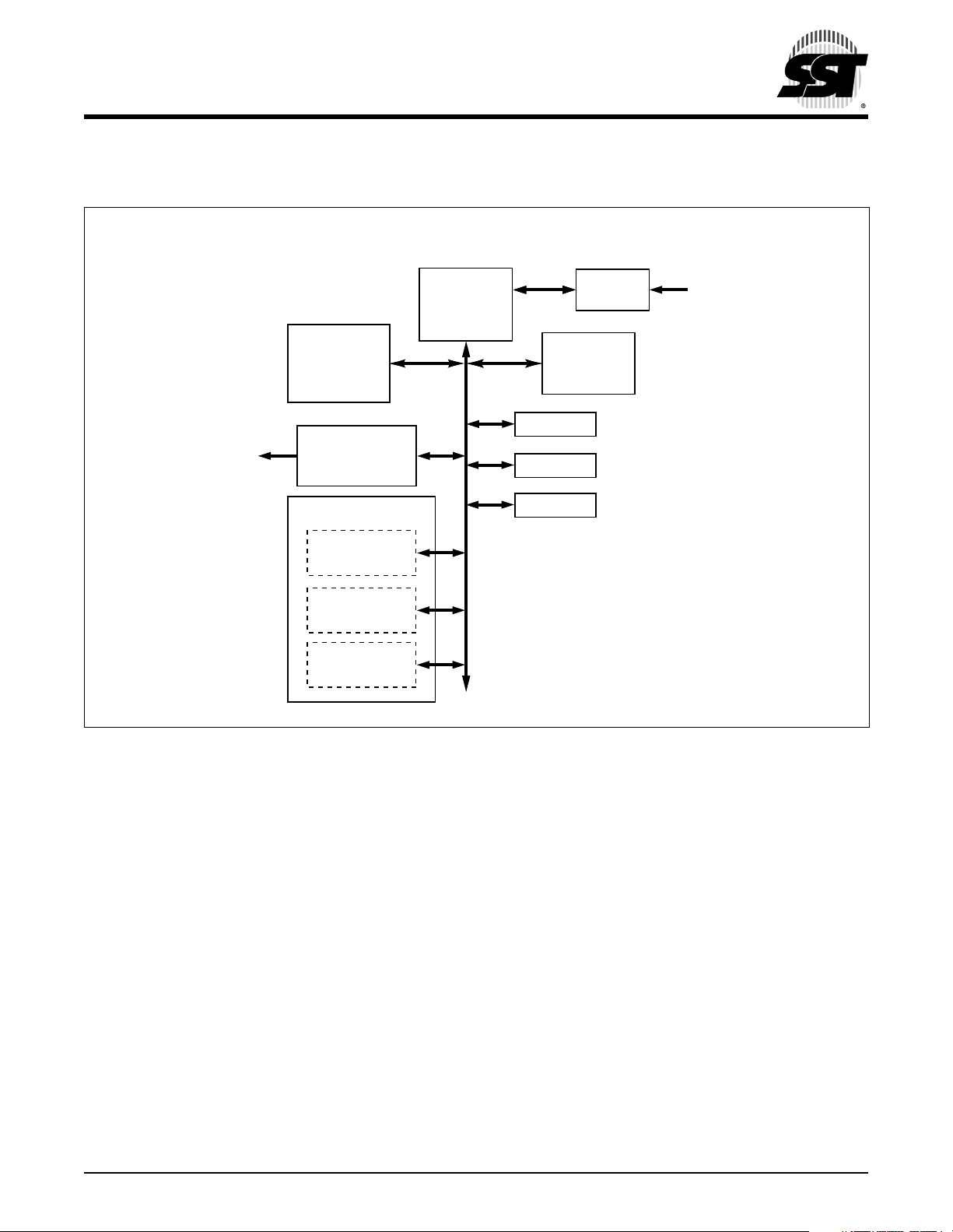
1.0 FUNCTIONAL BLOCKS
FUNCTIONAL BLOCK DIAGRAM
IRO
SuperFlash
Memory
16K x8
Carrier Modulator
Transmitter
Timer/Counter Interrupt
Real-Time
Counter
Core Timer
/ Counter
COP Watchdog
Timer
MCU Core
Por t A
Por t B
Por t C
Interrupt
Control
RAM
352K x8
IRQ#
368 ILL B1.8
©2001 Silicon Storage Technology, Inc. S71170-03-000 12/01 368
5
Page 6
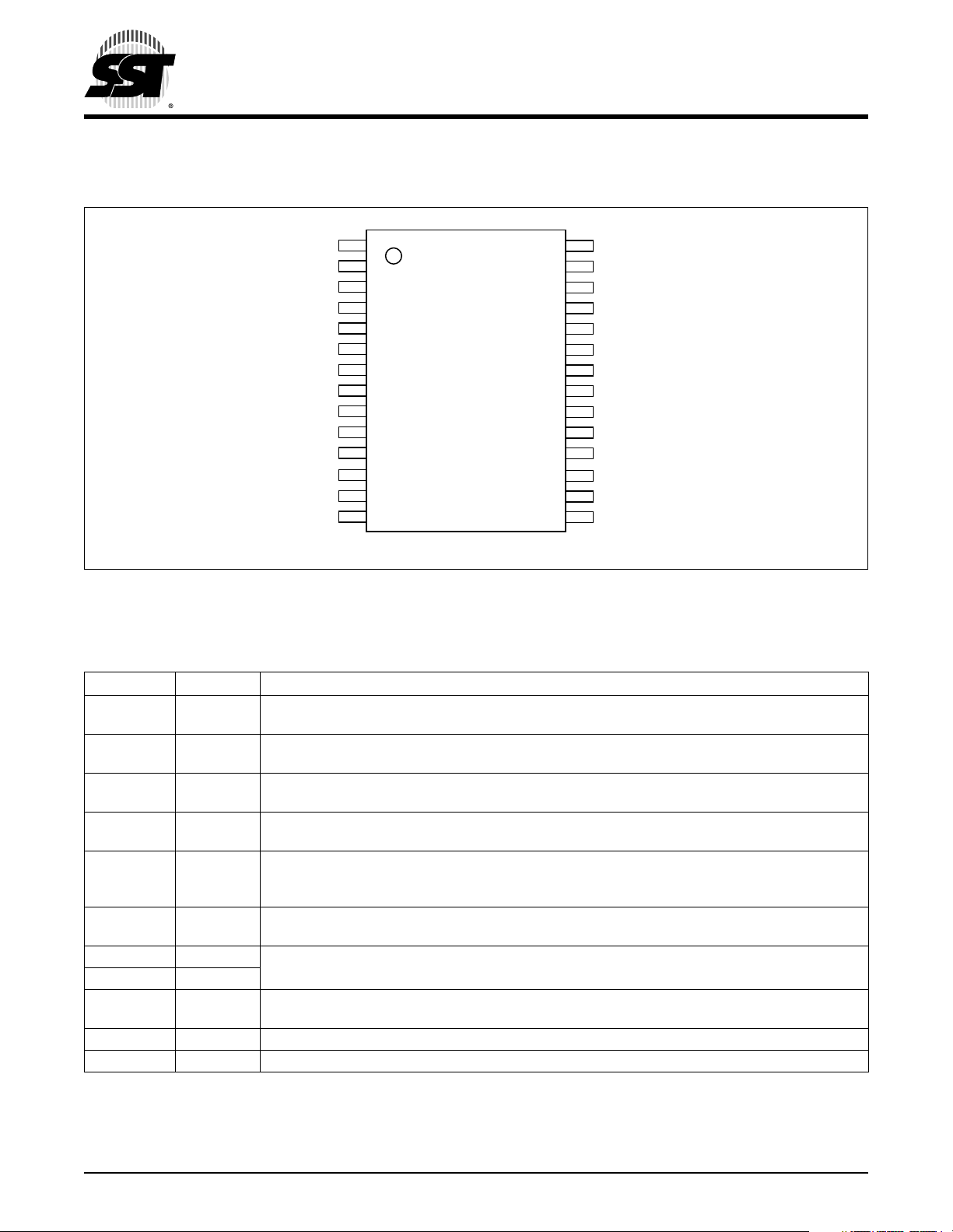
2.0 PIN ASSIGNMENTS
Remote Controller MCU
SST65P542R
Advance Information
PB0
PB1
PB2
PB3
PB4
PB5
PB6
PB7
PA 0
PA 1
PA 2
PA 3
PA 4
PA 5
1
2
3
4
5
6
7
8
9
10
11
12
13
14
28-lead SOIC
Top View
368 28-soic ILL P01.5
28
27
26
25
24
23
22
21
20
19
18
17
16
15
OSC1
OSC2
V
DD
IRQ#
RST#
IRO
V
SS
LPRST#
PC3
PC2
PC1
PC0
PA 7
PA 6
FIGURE 2-1: PIN ASSIGNMENTS FOR 28-LEAD SOIC
2.1 Pin Descriptions
TABLE 2-1: PIN DESCRIPTIONS
Symbol Type Name and Functions
PA[7:0] I/O
PB[7:0] I/O Por t B: The state of any pin in Port B is software programmable and every line is configured as an
PC[3:0] I/O Port C: Every pin in Port C is a high-current pin and its state is software programmable. All lines
IRO O IRO: Suitable for driving IR LED biasing logic, the IRO pin is the high-current source and sink out-
LPRST# I Low-Power Reset: An active-low pin, LPRST# function sets MCU to low-power reset mode. Once the
RST# I Reset: By setting the RST# pin low, the device is reset to a default state. An internal Schmitt trig-
OSC1 I Oscillator 1,2: These 2 pins interface with external oscillator circuits. A crystal
OSC2 O resonator, a ceramic resonator, or an external clock signal can be used.
IRQ# I Interrupt Request: The IRQ# is negative edge-sensitive triggered. An internal Schmitt trigger is
V
DD
V
SS
1. I = Input, O = Output
1
Port A: The state of any pin in Port A is software programmable and every line is configured as
an input during any reset.
input during any reset. Each I/O line contains a programmable interrupt/pull-up for keyscan.
are configured as inputs during any reset.
put of the carrier modulator transmitter subsystem. Default state is low after any reset.
device is in low-power reset mode, it is held in reset with all processor clocks and crystal oscillator halted.
An internal Schmitt trigger is included in the LPRST# pin to improve noise immunity.
ger is included in the RST# pin to improve noise immunity.
included in the IRQ# pin to improve noise immunity.
PWR Power Supply: Supply Voltage (2.2-3.2V)
PWR Ground: Circuit ground. (0V reference)
T2-1.14 368
©2001 Silicon Storage Technology, Inc. S71170-03-000 12/01 368
6
Page 7
Remote Controller MCU
SST65P542R
Advance Information
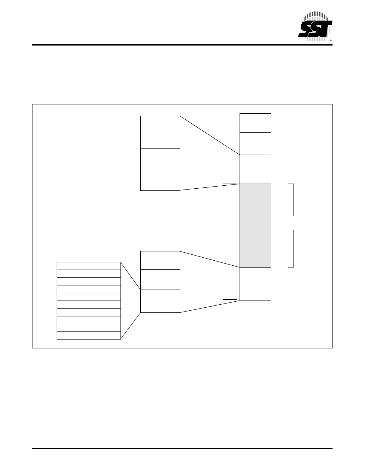
3.0 I/O REGISTERS AND MEMORY ORGANIZATION
The SST65P542R has a total of 64 KByte of addressable memory space. A memory map is located in Figure 3-1.
The on-chip memory consists of 32 Bytes of I/O registers, 352 Bytes of SRAM, 16 KByte of user flash memory and
128 Bytes of user vectors.
Core Timer Vector - (High Byte)
FFF6H
Core Timer Vector - (Low Byte)
FFF7H
FFF8H
FFF9H
FFFAH
FFFBH
FFFCH
FFFDH
FFFEH
FFFFH
CMT Vector (High Byte)
CMT Vector (Low Byte)
IRQ/Port B Vector (High Byte)
IRQ/Port B Vector (Low Byte)
SWI Vector (High Byte)
SWI Vector (Low Byte)
Reset Vector (High Byte)
Reset Vector (Low Byte)
Reserved
CWT Reset
Reserved
Flash Memory
Read Protection
Reserved
Reset and
Interrupt
Vectors
0180H
3FEFH
3FF0H
3FF1H
BFFFH
FF80H
FF81H
FFF5H
FFF6H
FFFFH
Flash Memory
(128 sectors)
I/O
Registers
352 Bytes
SRAM
User
Memory
16,256
Bytes
User
Vector
0000H
001FH
0020H
017FH
0180H
BFFFH
C000H
127 Sectors
(128 Bytes per sector)
FF7FH
FF80H
FFFFH
368 ILL F02.9
FIGURE 3-1: M
©2001 Silicon Storage Technology, Inc. S71170-03-000 12/01 368
EMORY MAP
7
Page 8
Remote Controller MCU
SST65P542R
Advance Information
3.1 I/O Registers
The 32 Bytes of I/O registers occupy address locations from 0000H to 001FH that include general purpose I/O registers, the SuperFlash Function Register, and on-chip peripheral control registers.
TABLE 3-1: R
1
Symbol
PORTA Port A Data
PORTB Port B Data
PORTC Port C Data
DDRA Port A Data
DDRB Port B Data
DDRC Port C Data
CTSCR Core Timer
CTCR Core Timer
PBIC Port B
SFFR SuperFlash
PBPUC Port B Pull-up
CWTC CWT Control
CHR1 Carrier
CLR1 Carrier
CHR2 Carrier
Description
Register
Register
Register
- Reserved 0003H - - - - - - - - -
Direction
Register
Direction
Register
Direction
Register
- Reserved 0007H - - - - - - - - -
Control and
Status
Register
Counter
Register
Interrupt
Control
Register
Function
Register
Control
Register
Register
- Reserved 000EH - - - - - - - - -
- Reserved 000FH - - - - - - - - -
Generator
High Data
Register 1
Generator
Low Data
Register 1
Generator
High Data
Register 2
EGISTER DESCRIPTIONS AND BIT DEFINITIONS (1 OF 2)
Direct
Address
0000H PA7 PA6 PA5 PA4 PA3 PA2 PA1 PA0 00H
0001H PB7 PB6 PB5 PB4 PB3 PB2 PB1 PB0 00H
0002H - - - - PC3 PC2 PC1 PC0 00H
0004H DDRA7 DDRA6 DDRA5 DDRA4 DDRA3 DDRA2 DDRA1 DDRA0 00H
0005H DDRB7 DDRB6 DDRB5 DDRB4 DDRB3 DDRB2 DDRB1 DDRB0 00H
0006H - - - - DDRC3 DDRC2 DDRC1 DDRC0 00H
0008H CTOF RTIF TOFE RTIE TOFC RTFC RT1 RT0 03H
0009H CTD7 CTD6 CTD5 CTD4 CTD3 CTD2 CTD1 CTD0 00H
000AH INPRB7 INPRB6 INPRB5 INPRB4 INPRB3 INPRB2 INPRB1 INPRB0 00H
000BH PREN MEREN SEREN - PROG MERA SERA - 00H
000CH - - - - - - PU1 PU0 03H
000DH - - - - - - - CWT_EN 00000001b
0010H IROLN CMTPOL PH5 PH4 PH3 PH2 PH1 PH0 00UUUUUUb
0011H IROLP - PL5 PL4 PL3 PL2 PL1 PL0 00UUUUUUb
0012H - - SH5 SH4 SH3 SH2 SH1 SH0 00UUUUUUb
Bit 7 Bit 6 Bit 5 Bit 4 Bit 3 Bit 2 Bit 1 Bit 0
Bit Address, Bit Symbol
Reset
Val ue
2,3
©2001 Silicon Storage Technology, Inc. S71170-03-000 12/01 368
8
Page 9
Remote Controller MCU
SST65P542R
Advance Information
TABLE 3-1: REGISTER DESCRIPTIONS AND BIT DEFINITIONS (CONTINUED) (2 OF 2)
1
Symbol
CLR2 Carrier
MCSR Modulator
MDR1 Modulator
MDR2 Modulator
MDR3 Modulator
PSCR Power
CWTC COP
1. “-” = reserved bits
2. “U” = unaffected by any reset
3. These registers can be reset by either external or internal reset.
Description
Generator
Low Data
Register 2
Control and
Status
Register
Data
Register 1
Data
Register 2
Data
Register 3
Saving
Control
Register
- Reserved 0019H - - - - - - - - -
- Reserved 001AH - - - - - - - - -
- Reserved 001BH - - - - - - - - -
- Reserved 001CH - - - - - - - - -
- Reserved 001DH - - - - - - - - -
- Reserved 001EH - - - - - - - - -
- Reserved 001FH - - - - - - - - -
Watchdog
Timer Reset
Register
Direct
Address
0013H - - SL5 SL4 SL3 SL2 SL1 SL0 00UUUUUUb
0014H EOC DIV2 EIMSK EXSPC BASE MODE EOCIE MCGEN 00H
0015H MB11 MB10 MB9 MB8 SB11 SB10 SB9 SB8 UUUUUUUUb
0016H MB7 MB6 MB5 MB4 MB3 MB2 MB1 MB0 UUUUUUUUb
0017H SB7 SB6 SB5 SB4 SB3 SB2 SB1 SB0 UUUUUUUUb
0018H EN - - - - - STOP IDL 10000011b
3FF0H - - - - - - - CWT_CLR 01H
Bit 7 Bit 6 Bit 5 Bit 4 Bit 3 Bit 2 Bit 1 Bit 0
Bit Address, Bit Symbol
Reset
Val ue
2,3
T3-1.8 368
©2001 Silicon Storage Technology, Inc. S71170-03-000 12/01 368
9
Page 10
PORT A Data Register (PORTA)
Location
0000H
76543210
PA 7 PA 6 PA 5 PA 4 PA 3 PA 2 PA 1 PA 0
Symbol Function
PA[7:0] Port A data register bit 0 to 7. These bits are for both reading and writing. Write the data to this
register will output data to port A pins when it’s in output mode. If the pins are set to input mode,
only the output data register is updated, port A pins are tri-stated. Reading the data from this
register will read the state of port A pins when set in input mode. If the pins are set to output
mode, it reads the output data register. See Table 3-2 for details. For a detailed explanation of
each parallel I/O port, please refer to Section 4.0, “Parallel Input/Output Ports” on page 20.
PORT B Data Register (PORTB)
Location
0001H
76543210
PB7 PB6 PB5 PB4 PB3 PB2 PB1 PB0
Symbol Function
PB[7:0] Port B data register bit 0 to 7. These bits are for both reading and writing. Writing data to this
register will output data to port B pins when it’s in output mode. If the pins are set to input mode,
only the output data register is updated, port B pins are tri-stated. Reading the data from this
register will read the state of port B pins when set in input mode. If the pins are set to output
mode, it reads the output data register. See Table 3-2 for details.
Remote Controller MCU
SST65P542R
Advance Information
Reset Value
00H
Reset Value
00H
PORT C Data Register (PORTC)
Location
0003H
76543210
- - - - DDRC3 DDRC2 DDRC1 DDRC0
Symbol Function
PC[3:0] Port C data register bit 0 to 3. These bits are for both reading and writing. Writing data to this
register will output data to port C pins when it’s in output mode. If the pins are set to input mode,
only output data register is updated, port C pins are tri-stated. Reading data from this register will
read the state of port C pins when set in input mode. If the pins are set to output mode, it reads
the output data register. See Table 3-2 for details.
TABLE 3-2: I/O PIN FUNCTIONS AS GENERAL PURPOSE I/O
Access DDRA, DDRB, DDRC Mode I/O Pin Functions
Write 0 Input Data is written into the output data register.
Write 1 Output Data is written into the output data register and
Read 0 Input The state of I/O is read
Read 1 Output The output data register is read
Reset Value
00H
output to the I/O pins.
T3-2.0 368
©2001 Silicon Storage Technology, Inc. S71170-03-000 12/01 368
10
Page 11
Remote Controller MCU
SST65P542R
Advance Information
PORT A Data Direction Register (DDRA)
Location
0004H
PORT B Data Direction Register (DDRB)
Location
0005H
76543210
DDRA7 DDRA6 DDRA5 DDRA4 DDRA3 DDRA2 DDRA1 DDRA0
Symbol Function
DDRA[7:0] Port A data direction register bit 0 to 7. These bits are for both reading and writing.
See Table 3-2 for details.
0: Port A is input
1: Port A is output
76543210
DDRB7 DDRB6 DDRB5 DDRB4 DDRB3 DDRB2 DDRB1 DDRB0
Symbol Function
DDRB[7:0] Port B data direction register bit 0 to 7. These bits are for both reading and writing.
See Table 3-2 for details.
0: Port B is input
1: Port B is output
Reset Value
00H
Reset Value
00H
PORT C Data Direction Register (DDRC)
Location
0006H
76543210
----PC3PC2PC1PC0
Symbol Function
DDRC[3:0] Port C data direction register bit 0 to 3. These bits are for both reading and writing.
See Table 3-2 for details.
0: Port C is input
1: Port C is output
PORT B Interrupt Control Register (PBIC)
Location
000AH
76543210
INPRB7 INPRB6 INPRB5 INPRB4 INPRB3 INPRB2 INPRB1 INPRB0
Symbol Function
INPRB[7:0] Port B interrupt control bits
0: Interrupt is enabled
1: Interrupt is disabled
Reset Value
00H
Reset Value
00H
©2001 Silicon Storage Technology, Inc. S71170-03-000 12/01 368
11
Page 12
PORT B Pull-up Control Register (PBPUC)
Location
000CH
76543210
------PU1PU0
Symbol Function
PU1,PU0 Port B pull-up control bits. The following table shows pull-up strength.
Defaults to strong pull-up when reset.
TABLE 3-3: PULL-UP CONTROL BIT DESCRIPTION
PU1 PU0 Pull-up
0 0 No pull-up for Port B bit
0 1 Weak pull-up for each Port B bit
1 0 Weak pull-up for each Port B bit
1 1 Strong pull-up for each Port B bit
1. Default value after Power-on or Reset
Remote Controller MCU
SST65P542R
Advance Information
Reset Value
03H
1
T3-3.1 368
©2001 Silicon Storage Technology, Inc. S71170-03-000 12/01 368
12
Page 13

Remote Controller MCU
SST65P542R
Advance Information
Core Timer Control Status Register (CTCSR)
Location
0008H
76543210
CTOF RTIF TOFE RTIE TOFC RTFC RT1 RT0
Symbol Function
CTOF Core timer overflow bit. CTOF is a real-only status bit, this bit is set when the 8-bit ripple counter
rolls over from FFH to 00H. Writing to this bit has not effect. Reset clears CTOF. CTOF set to
zero by writing a one to TOFC.
RTIF Real-time Interrupt bit. RTIF is a read-only status bit. Writing has no effect on this bit. Reset
clears RTIF. The real time interrupt circuit consists of a divider and a one-of-four selector. The
input clock frequency that drives the RTI circuit is E/2
allows a maximum interrupt period of 16 ms at the internal peripheral clock rate of 2.048 MHz.
0: Writing a one to RTFC clears the RTIF.
1: When the output of the chosen (one-of-four selector) stage goes active.
TOFE Timer overflow enable bit. TOFE is statuses bit for both read and write. Reset clears this bit.
0: If the CTOF is not set or no timer overflow occurs.
1: If the CTOF is set and a CPU interrupt request is generated
RTIE Real time interrupt enable bit. RTIE is a status bit for both read and write. Reset clears this bit.
0: If the RTIF is not set.
1: If the RTIF is set and a CPU interrupt request is generated.
TOFC Timer overflow flag clear bit. This bit is for writing only.
0: Writing a zero has no effect on the CTOF bit. This bit always reads as zero.
1: When a one is written to this bit, CTOF is cleared.
RTFC Real time interrupt flag clear bit. This bit is for writing only.
0: Writing a zero has no effect on the RTIF bit. This bit always reads as zero.
1: When a one is written to this bit, RTIF is cleared.
RT[1:0] Real time interrupt rate select bit. These two bits select one of four taps from the interrupt logic.
See Table 3-4. Reset sets these two bits, which selects the lowest periodic rate and gives the
maximum. Care should be taken when altering RT0 and RT1 if the timeout period is imminent or
uncertain. The CWT should be cleared before changing RTI taps. If the selected tap is modified
during a cycle in which the counter is switching, an RTIF could be missed or an additional one
could be generated.
Reset Value
03H
12
with three additional divider stages that
TABLE 3-4: RTI AND CWT RATES AT 4.096 MHZ OSCILLATOR, PRESCALER=1
RTI Rate RT1-RT0 Minimum CWT Rates Maximum CWT Rates
2ms 2
4ms 213/E 01 (216-213)/E 28ms (216)/E 32ms
8ms 214/E 10 (217-214)/E 56ms (217)/E 64ms
16ms 2
1. E is the internal peripheral clock frequency and E = F
©2001 Silicon Storage Technology, Inc. S71170-03-000 12/01 368
12/E1
15
/E 11 (218-215)/E 112ms (218)/E 128ms
00 (215-212)/E 14ms (215)/E 16ms
T3-4.2 368
13
OSC
/2
Page 14

Remote Controller MCU
SST65P542R
Advance Information
Core Timer Counter Register (CTCR)
Location
0009H
SuperFlash Function Register (SFFR)
Location
000BH
Therefore, when SFFR=22H, the MCU will perform the Sector-Erase, SFFR=44H, the MCU will perform the ChipErase, and SFFR=88H, the MCU will perform the Byte-Program. For a detailed explanation of MCU flash control,
please refer to Section 5.1, “In-Application Programming” on page 21.
76543210
CTD7 CTD6 CTD5 CTD4 CTD3 CTD2 CTD1 CTD0
Reset Value
00H
Symbol Function
CTD[7:0] The core timer counter register bit 0 to bit 7. This is a read only status register in which contains
the current value of the 8-bit ripple counter. This counter is clocked by the CPU clock (E/4) and
can be used for various functions, including a software input capture. Extended time can be
achieved by using the timer overflow function to increment a variable to simulate a 16-bit
counter.
76543210
PREN MEREN SEREN - PROG MERA SERA -
Reset Value
00H
Symbol Function
PREN Byte program enable bit.
0: Disable the byte program.
1: Enable the byte program.
MEREN Mass (chip) program enable.
0: Disable the mass (chip) erase or program.
1: Enable the mass (chip) erase or program.
SEREN Sector program enable.
0: Disable the sector erase or program.
1: Enable the sector erase or program.
PROG Byte program control bit.
0: Not performs the byte program
1: Performs the byte program.
MERA Mass (chip) program active bit.
0: Not performs the chip program
1: Performs the chip program.
SERA Sector program active bit.
0: Not performs the sector program.
1: Performs the sector program.
©2001 Silicon Storage Technology, Inc. S71170-03-000 12/01 368
14
Page 15

Remote Controller MCU
SST65P542R
Advance Information
COP Watchdog Timer Control Register (CWTC)
Location
000DH
COP Watchdog Timer Reset Register (CWTR)
Location
3FF0H
76543210
-------CWT_EN
Symbol Function
CWT_EN COP watchdog timer enable bit.
0: COP watchdog timer is enabled.
1: COP watchdog timer is disabled.
76543210
-------
Symbol Function
CWT_CLR This bit is for writing only. For detail explanation of COP Watchdog Timer Reset, please refer to
Section 6.4
0: Write zero to this bit will clear COP watchdog timer.
1: Write one to this bit has no effect. Read this bit will always returns one.
CWT_CLR
Reset Value
01H
Reset Value
01H
Carrier Generator High Data Register1 (CHR1)
Location
0010H
76543210
IROLN CMTPOL PH5 PH4 PH3 PH2 PH1 PH0
Symbol Function
IROLN IRO latch control bit. Reading IROLN bit reads the state of the IRO latch. Writing IROLN updates
the IRO latch with the data being written on the negative edge of the internal processor clock
/2). The IRO latch is clear out of reset. Writing to CHR1 to update IROLN will also update
(F
OSC
the primary carrier high data value. In addition, writing to CHR1 to update IROLN will update the
CMT polarity bit. Bit 6 should contain the data of CMTPOL polarity bit.
CMTPOL CMT output polarity bit. This bit controls the polarity of the CMT output (IRO).
0: the CMT output is active high.
1: the CMT output is active low.
PH[5:0] Primary carrier high time data values. When selected, these bits contain the number of input
clocks required to generate the carrier high time periods. When operating in timer mode, CHR1
and CLR1 are always selected. When operating in FSK mode, CHR1, CLR1 and CHR2, CLR2
are alternately selected under control of the modulator. The primary carrier high and low time
values are undefined on the reset. These bits must be written to non-zero values that before the
carrier generator is enabled to avoid spurious results.
Bit 0 to Bit 7 of CHR1 can be used for both reading and writing.
Note:“U” indicates that the bit is unaffected after reset.
Reset Value
00UUUUUUb
©2001 Silicon Storage Technology, Inc. S71170-03-000 12/01 368
15
Page 16

Carrier Generator Low Data Register1 (CLR1)
Location
0011H
76543210
IROLP - PL5 PL4 PL3 PL2 PL1 PL0
Symbol Function
IROLP IRO latch control bit. Reading IROLP bit reads the state of the IRO latch. Writing IROLP updates
the IRO latch with the data being written on the negative edge of the internal processor clock
/2). Writing to CLR1 to update IROLP will also update the primary carrier low data value.
(F
OSC
Care should be taken that bits 5-0 of the data to be written to CHR1 or CLR1.
PL[5:0] Primary carrier low time data values. The function of these bits is the same as PH[5:0].
Carrier Generator High Data Register2 (CHR2)
Location
0012H
76543210
- - SH5 SH4 SH3 SH2 SH1 SH0
Symbol Function
SH[5:0] Secondary carrier high time data values. When selected, these bits contain the number of input
clocks required to generate the carrier high time periods. When operating in time mode, CHR2
and CLR2 is never selected. When operating in FSK mode, CHR2, CLR2 and CHR1, CLR1 are
alternately selected under control of the modulator. The secondary carrier high and low time
values are undefined on the reset. These bits must be written to nonzero values before the
carrier generator is enabled when operating in FSK mode.
Remote Controller MCU
SST65P542R
Advance Information
Reset Value
00UUUUUUb
Reset Value
00UUUUUUb
Carrier Generator Low Data Register2 (CLR2)
Location
0013H
76543210
- - SL5 SL4 SL3 SL2 SL1 SL0
Symbol Function
SL[5:0] Secondary carrier low time data values. The function of these bits is the same as SH[5:0].
Reset Value
00UUUUUUb
©2001 Silicon Storage Technology, Inc. S71170-03-000 12/01 368
16
Page 17

Remote Controller MCU
SST65P542R
Advance Information
Modulator Control and Status Register (MCSR)
Location
0014H
76543210
EOC DIV2 EIMSK EXSPC BASE MODE EOCIE MCGEN
Symbol Function
EOC End of modulation cycle status bit. This bit is read only. EOC is set when a match occurs
between the contents of the space period register SREG and the down counter. At the end of
cycle, the counter is initialized with the contents of the mark period buffer, MBUFF and SREG is
loaded with the space period buffer SBUFF. This flag is cleared by reading the MCSR followed
by an access of MDR2 or MDR3. EOC is cleared by reset.
0: current modulation cycle in progress.
1: end of modulator cycle has occurred.
DIV2 Divide by two scaler bit. The divide-by-two prescaler causes the CMT to be clocked at the bus
rate, when the two times of bus rate is enabled and the F
double buffered, this bit should not be set during a transmission.
0: divide-by-two prescaler disabled.
1: divide-by-two prescaler enabled.
EIMSK External Interrupt Mask bit. This bit is used to mask IRQ and keyscan interrupts. This bit is
cleared by reset.
0: IRQ and keyscan interrupts enabled.
1: IRQ and keyscan interrupts disabled.
EXSPC Extended Space Enable bit. For detailed description of extended space operation, please refer
to 65P542R Programming User’s Manual.
0: Extended space disabled.
1: Extended space enabled
BASE Baseband Enable bit. This bit disables the carrier generator and forces the carrier output high for
generation of baseband protocols. When BASE is cleared, the carrier generator is enabled and
the carrier output toggles at the frequency determined by values stored in the carrier data
registers. This bit is cleared by reset. This bit is not double buffered and should not be written
during a transmission.
0: Baseband disabled.
1: Baseband enabled.
MODE Mode select bit. This bit is cleared by reset. This bit is not double buffered and should not be
written during a transmission.
0: CMT operates in Time mode.
1: CMT operates in FSK mode.
EOCIE Interrupt enable bit. Interrupt request will be generated when EOC is set and EOCIE is set.
Otherwise, interrupt will not be generated
0: interrupt disabled.
1: interrupt enabled.
MCGEN Modulator and carrier generator enable bit. Set this bit will initialize the carrier and modulator and
will enable all clocks. Once enabled, the carrier generator and modulator will function
continuously.
0: if this bit is zero, the current modulator cycle will be allowed to expire before all carrier and
modulator clocks are disabled and the modulator output is forced low. To prevent spurious
operation, the user should initialize all data and control registers before enabling the system.
This bit is cleared by reset.
All bits except Bit 0 can be used for both reading and writing.
1: Modulator and carrier generator enabled.
Reset Value
00H
is disabled. Since this bit is not
OSC
©2001 Silicon Storage Technology, Inc. S71170-03-000 12/01 368
17
Page 18

Modulator Data Register 1 (MDR1)
Location
0015H
76543210
MB11 MB10 MB9 MB8 SB11 SB10 SB9 SB8
Symbol Function
MB[11:8] MBUFF high 4 bits.
SB[11:8] SBUFF high 4 bits.
These bits can be used for both reading and writing.
Modulator Data Register 2 (MDR2)
Location
0016H
76543210
MB7 MB6 MB5 MB4 MB3 MB2 MB1 MB0
Symbol Function
MB[7:0] MBUFF lower 8 bits. These bits can be used for both reading and writing.
Modulator Data Register 3 (MDR3)
Location
0016H
76543210
SB7 SB6 SB5 SB4 SB3 SB2 SB1 SB0
Remote Controller MCU
SST65P542R
Advance Information
Reset Value
UUUUUUUUb
Reset Value
UUUUUUUUb
Reset Value
UUUUUUUUb
Symbol Function
SB[7:0] SBUFF lower 8 bits. The bits can be used for reading and writing.
Power Saving Control Register (PSCR)
Location
0018H
76543210
EN-----STOPIDL
Symbol Function
EN This bit enable or disable MCU to stop and idle mode. This bit can be used for both reading and
writing.
0: STOP and IDLE mode enable
1: STOP and IDLE mode disable.
STOP Stop mode enable bit
0: write 0 to this bit will make the device entering the stop mode if EN=0
1: write 1 to this bit has no effect. Read returns one.
IDL Idle mode enable bit
0: write 0 to this bit will make the device entering the idle mode if EN=0
1: write 1 to this bit has no effect. Read returns one.
Reset Value
10000011b
©2001 Silicon Storage Technology, Inc. S71170-03-000 12/01 368
18
Page 19

Remote Controller MCU
SST65P542R
Advance Information
3.2 SRAM
There are 352 Bytes of SRAM available. The SRAM
addresses start from location 0020H to 017FH. The stack
pointer can address 64 Bytes of stack beginning at address
location 00FFH and ending at 00C0H.
3.3 SuperFlash Memory
The SST65P542R has 16 KByte of SuperFlash EEPROM
memory. The memory is organized as 128 sectors of 128
Bytes each. The minimum erasable memory unit is one
sector or 128 Bytes. The user programmable flash memory
occupies the address space from C000H to FF7FH. The
user vector area consists of 128 Bytes starting from
address location FF80H to FFFFH. Address FF80H is for
flash memory read protection. There are five predetermined user vectors from FFF6H through FFFFH dedicated
to the reset and interrupts. Every vector consists of two
bytes to be loaded into program counter for jumping to an
interrupt service routine (ISR). See Table 3-5 for detailed
descriptions of these vectors.
TABLE 3-5: I
Address
Location User Vectors
FF80H Flash Memory Read Protection
FF81H-FFF5H Unused
FFF6H Core Timer Vector - (High Byte)
FFF7H Core Timer Vector - (Low Byte)
FFF8H CMT Vector (High Byte)
FFF9H CMT Vector (Low Byte)
FFFAH IRQ/Port B Vector (High Byte)
FFFBH IRQ/Port B Vector (Low Byte)
FFFCH SWI Vector (High Byte)
FFFDH SWI Vector (Low Byte)
FFFEH Reset Vector (High Byte)
FFFFH Reset Vector (Low Byte)
NTERRUPT/RESET SECTOR
T3-5.5 368
©2001 Silicon Storage Technology, Inc. S71170-03-000 12/01 368
19
Page 20

4.0 PARALLEL INPUT/OUTPUT PORTS
Remote Controller MCU
SST65P542R
Advance Information
4.1 Port A
Port A consists of eight individual pins driven by one data
register and one direction register to control the usage of
these pins as either inputs or outputs. All Port A pins are set
to Input mode during any Reset. Software must set the
right direction register first before performing any Read or
Write operation. Any Read operation to the port that was
set as output will read back the data from an internal latch
register instead of the I/O pins. For details, please refer to
Section 3.1 Port A data register and Port A data direction
register.
V
DD
WEAK0
WEAK1
PU0
PU1
4.2 Port B
Port B pins are similar to Port A pins except that each of the
Port B pins has a programmable interrupt generation
option which can be enabled for any Port B pins. Port B
pins have optional programmable pull-ups. There is a
choice between pull-up strengths which could be selected
by PU0 or PU1. For details, please refer to Section 3.1, Port
B Interrupt Control Register and Port B Pull-up Control
Register.
INPRB7
DDRB7
PB7
FIGURE 4-1: P
ORT B INTERRUPT AND PULL-UP OPTIONS
4.3 Port C
Port C is a 4-bit bi-directional port (PC3-PC0). Every Port C
pin has high current driving capability. Reset clears the Port
C Data Register and the data direction register, thereby
returning the ports to inputs. For details, please refer to
Section 3.1 Port C data register and Port C data direction
register.
From all other Port B Pins
.
.
.
Interrupt
Logic
368 ILL F03.3
©2001 Silicon Storage Technology, Inc. S71170-03-000 12/01 368
20
Page 21

Remote Controller MCU
SST65P542R
Advance Information
5.0 FLASH MEMORY PROGRAMMING
5.1 In-Application Programming
SST65P542R allows “In-Application Programming” (IAP)
to update the user code in the internal 16 Kbyte SuperFlash memory. All Write/Erase operations require setting
the enable bit in the SuperFlash Function Register (SFFR)
located at 000BH. The following sections describe the
operations that the MCU performs to alter the contents of
SuperFlash Memory. For detailed explanation of the SuperFlash Function Register, please refer to Section 3.1.
5.1.1 Chip-Erase
The Chip-Erase operation requires MEREN and MERA
bits to be set to logical “1”. After setting these bits, writing
any data to any address location of the flash memory will
trigger the Chip-Erase operation. The MCU is idle while
SST65P542R is busy doing erases on all memory locations.
5.1.2 Sector-Erase
The Sector-Erase operation requires SEREN and SERA
bits to be set to logical “1”. After setting these bits, writing
any data to the address within the sector to be erased will
erase the data in the sector. The MCU is idle while
SST65P542R is busy doing erase on the sector.
5.1.3 Byte-Program
The Byte-Program operation requires PREN and PROG
bits to be set to logical “1”. After setting these bits, and then
writing the data to the target address to be programmed.
The MCU is idle while SST65P542R is busy doing programming on the byte. Refer to the following summary for
all different functions.
.
TABLE 5-1: SFFR C
Command
Writes to
Function
Chip-Erase 44H Erase the whole flash memory
Sector-Erase 22H Erase the sector
Byte-Program 88H Program one data byte to
SFFR Comment
OMMANDS
addressed by CXXXH
address CXXXH.
Write data to CXXXH
before Byte-Program can be
performed, a Chip-Erase or
Sector-Erase must be issued
to erase the target
programming locations.
T5-1.1 368
5.2 External Host Programming Mode
The external host programming mode is to provide programmer access to the 16KB embedded flash memory of
the SST65P542R. To enter the external host programming
mode, users must follow the setup sequences on the pins
(See Figure 11-1):
1. RY/BY# (pin 12) and POROUT# (pin 13) are output pins. Do not drive.
2. Drive RST# (pin 24) low.
3. Drive LPRST# (pin 21) low.
4. Drive LPRST# (pin 21) high after T
5. Drive PROG_RST (pin 9) low.
6. Drive 9 clocks on TCLKIN. On each clock's rising
edge provide one bit of data on TDIN (pin 19) as
shown in Figure 11-1. The data bits are
“11010011”.
7. Wait for RY/BY# (pin 12) and POROUT# to go
high.
8. Drive at least 24 clocks on TCLKIN.
9. If Read-protect byte is set, then RY/BY# will go
low. Otherwise, RY/BY# will stay high. If RY/BY# is
low, wait for RY/BY# (pin 12) to go high. Now the
SST65P542R is in external host programming
mode and is ready for embedded flash Read or
Write operations.
Now the SST65P542R is in the external host programming
mode and is ready for embedded flash by the external host
Read or Write.
As soon as the RST# is released to ‘1’, chip exits external
host programming mode and then enters user mode.
5.2.1 External Host Mode Read Operation
As shown in Figure 11-2, the Read operation needs two
address setup cycles and one data setup cycle. The low to
high transition on SCLK latches the high order address
A[13:8] from the pin AD[5:0] while MODE[1:0] inputs are
set to 0H; the low to high transition on SCLK latches the
low order address A[7:0] from the pin AD[7:0] while the
MODE[1:0] inputs are set to 3H and setting the signal OE#
to low; the low to high transition on SCLK latches the data
D[7:0] on the pin AD[7:0] while the MODE[1:0] is set to 1H
for reading. After reading the data, the external host should
set the signal OE# to high.
RST
.
©2001 Silicon Storage Technology, Inc. S71170-03-000 12/01 368
21
Page 22

Remote Controller MCU
SST65P542R
Advance Information
5.2.2 External Host Mode Write Operation
As shown in Figure 11-3, the Write operation needs two
address setup cycles and one data setup cycle. The low to
high transition on SCLK latches the high order address
A[13:8] from the pin AD[5:0] while the MODE[1:0] inputs
are set to 0H; the low to high transition on SCLK latches the
TABLE 5-2: E
Pins Symbol Type
8-1 AD[7:0] I/O
10,20 MODE[1:0] I Address and data bus selection bits in the external host programming mode
11 SLCK I Clock for latch address and data after entering the external host programming mode
9 PROG_RST I Reset signal for the external host programming mode
13 POROUT# O Embedded flash memory power-on reset output
12 RY/BY# O Embedded flash Ready/Busy output. High is ready
17 WE# I Write Enable: embedded flash memory data write enable, low active
18 OE# I Output Enable: embedded flash memory data out enable, low active
21 LPRST# I Signal for entering the external host programming mode
19 TDIN I Data input for entering the external host programming mode
23 TCLKIN I This clock will latch TDIN for entering the external host programming mode
22 V
26 V
1. I = Input; O = Output
XTERNAL HOST PROGRAMMING MODE PIN DESCRIPTIONS
1
Name and Functions
1
Embedded flash memory address and data bus multiplex on AD[7:0] by selecting MODE[1:0]
SS
DD
PWR Ground: Circuit ground (0V reference)
PWR Power Supply: Supply voltage (3.2V)
low order address A[7:0] from the pin AD[7:0] while
MODE[1:0] inputs are set to 2H; the low to high transition
on SCLK latches the data D[0:7] from the pin AD[7:0] while
the MODE[1:0] is set to 1H for writing. However, the actual
Write operation to embedded flash memory occurs on the
rising edge of WE#.
T5-2.3 368
5.2.3 External Host Mode Byte-Program Operation
This device is programmed on a byte by byte basis. The
Byte-Program operation consists of three steps. The first
step is the three-byte load sequence for Software Data Protection. The second step is to load the byte address and
the byte data. The third step is the internal Program operation which is initiated after the rising edge of the fourth
WE#. The end of the Byte-Program operation can be
determined by using the RY/BY#. Any commands written
during the Byte-Program operation will be ignored. See
Table 5-4 for the software command sequence, Figure 11-5
for the flash Byte-Program timing diagram, and Figure 11-9
for the Byte-Program command sequence flowchart.
5.2.4 External Host Mode Chip-Erase Operation.
The device provides a Chip-Erase operation, which allows
the user to erase the entire memory array to the ’1’s state.
This is useful when the device must be quickly erased
entirely. The Chip-Erase operation is initiated by executing
a six-byte Software Data Protection command sequence,
the last byte Sequence is the address 1555H with the ChipErase command 10H. The Chip-Erase operation begins
with of the sixth write enable’s (WE#) rising edge. The end
of the Chip-Erase can be determined by using the signal
RY/BY#. Any commands written during the Chip-Erase
operation will be ignored. See Table 5-4 for the software
command sequence, Figure 11-4 for the flash Chip-Erase
timing diagram, and Figure 11-11 for the Chip-Erase command sequence flowchart.
5.2.5 External Host Mode Sector-Erase Operation
The Sector-Erase operation allows the system to erase the
device on a sector-by-sector basis. The sector architecture
is based on uniform sector size of 128 Bytes. The SectorErase operation is initiated by executing a six-byte command sequence for Software Data Protection, the last byte
sequence is the sector address SA with the Sector-Erase
command 30H. The address lines A[13:7] will be used to
determine the sector address. The internal Erase operation
begins after the sixth write enable’s (WE#) rising edge. The
End-of-Erase can be determined by using the signal RY/
BY#. Any commands written during the Sector-Erase operation will be ignored. See Table 5-4 for the software command sequence, Figure 11-5 for the flash Sector-Erase
timing diagram, and Figure 11-11 for the Sector-Erase
command sequence flowchart.
©2001 Silicon Storage Technology, Inc. S71170-03-000 12/01 368
22
Page 23

Remote Controller MCU
SST65P542R
Advance Information
5.2.6 Operation Status Detection - Program Timer
Method
During the Program or Erase operation, the programmer
can use the timer to decide the completion of the operation.
When a Program or Erase operation is started, system setup a timer for T
Erase), and T
SE
(for Byte-Program), T
BP
(for Sector-Erase) time period. After this
(for Chip-
SCE
timer time-out, the operation is completed. See Figure 1110 for Program Timer flowchart.
5.2.7 Operation Status Detection - RY/BY# Method
During the internal Program or Erase operation, the signal
RY/BY# indicates the status of the operation. When the
internal Program or Erase operation is in progress, the signal RY/BY# will be driven low. When the internal Program
or Erase operation is completed, the signal RY/BY# will be
driven high. The device is then ready for the next operation.
See Figure 11-10 for the Program Timer flowchart.
5.2.8 Exiting The External Host Programming Mode
To exit the external host programming mode, the external
host must set the RST# pin to high, and the PROG_RST is
reset to high. The device will exit the host programming and
enter the user mode. The MCU starts execution codes out
of the User Memory Space from the reset vector.
5.2.9 Flash Read Protection
To protect the program code from piracy the flash memory
location 3F80H (user memory address FF80H, flash memory is mapped to C000H through FFFFH, see Figure 3-1)
is evaluated by the internal hardware to determine the read
protect mode state. During this evaluation period, only the
RY/BY# pin is valid and all other pins are blocked. If this
byte is A3H (read protect is active), a Chip-Erase will be
performed by internal hardware before the external host
programming mode is activated. While the Chip-Erase
could take T
(See Table 11-5) as maximum time, users
SCE
may use RY/BY# pin to determine the completion of the
Chip-Erase. If this byte is not A3H (not read protected), all
of the flash memory are visible by using the external host
programming. During the internal Program or Erase operation, the signal RY/ BY# indicates the status of the operation. When the internal Program or Erase operation is in
progress, the RY/BY# will be driven low. When the internal
Program or Erase operation is completed, the RY/BY# will
be driven high. The device is then ready for the next operation. See Figure 11-10 for the Program Timer flowchart.
Note: After writing A3H to the flash read protection
register, the device needs to continue power-on
prior to finishing the programming function.
The programming function may include the
Program-Verify function.
TABLE 5-3: E
AD[0] Input A8 Input A0 Input D0 Output D0
AD[1] Input A9 Input A1 Input D1 Output D1
AD[2] Input A10 Input A2 Input D2 Output D2
AD[3] Input A11 Input A3 Input D3 Output D3
AD[4] Input A12 Input A4 Input D4 Output D4
AD[5] Input A13 Input A5 Input D5 Output D5
AD[6] Input A6 Input D6 Output D6
AD[7] Input A7 Input D7 Output D7
XTERNAL HOST PROGRAMMING MODE PIN ASSIGNMENT
MODE0=0
MODE1=0
MODE0=0
MODE1=1
MODE0=1
MODE1=0
MODE0=1
MODE1=1
T5-3.1 368
TABLE 5-4: SOFTWARE COMMAND SEQUENCE
1st Bus Write
Addr
Cycle
1
Data Addr1Data Addr1Data Addr1Data Addr1Data Addr1Data
Command
Sequence
Sector-Erase 1555H AAH 2AAAH 55H 1555H 80H 1555H AAH 2AAAH 55H SA
Chip-Erase 1555H AAH 2AAAH 55H 1555H 80H 1555H AAH 2AAAH 55H 1555H 10H
Byte-Program 1555H AAH 2AAAH 55H 1555H A0H WA
1. Address format A13-A0 (Hex)
2. SAX for Sector-Erase; uses A13-A7 address lines
3. WA = Program Byte address
2nd Bus Write
Cycle
3rd Bus Write
Cycle
4th Bus Write
Cycle
3
Data
5th Bus Write
Cycle
6th Bus Write
Cycle
2
30H
X
T5-4.3 368
©2001 Silicon Storage Technology, Inc. S71170-03-000 12/01 368
23
Page 24

Remote Controller MCU
SST65P542R
Advance Information
6.0 RESET
The 65P542R can be reset from five sources: two external inputs and three internal restart conditions.
FIGURE 6-1: R
OSC
Data
Address
Address
RST#
LPRST#
ESET BLOCK DIAGRAM
COP
Watchdog
Reset
Illegal
Address
Reset
6.1 External Reset
A low-level input on the RST# pin causes the program
counter to be set to the contents of location FFFEH and
FFFFH (Reset Vector). The MCU is initialized to a known
state. Stack pointer will be reset to FFH. Hardware Reset
is the highest priority input to the chip. An internal Schmitt
trigger is implemented on the RST# input to enhance the
noise immunity.
6.2 External Low Power Reset
The LPRST# is one of the two external sources of a reset.
The signal LPRST# allows the MCU to go into low power
reset mode. All clocks and oscillator to the processor are
halted when the LPRST# is held low. After the LPRST# is
de-asserted (driven high), a delay of 4064 bus clock cycles
is automatically enabled to wait for stable crystal oscillation.
This pin also implements an internal Schmitt trigger to
enhance the noise immunity.
6.3 Internal Power-on and Brown-out
Reset
The internal reset signal will reset the CPU and all
peripheral components. Please refer to Figure 6-1. When
the device is powered up, the internal power-up voltage is
2.0-2.2V. In addition, the internal brown-out voltage is set
Reset
Control
4064 Bus
Clock Cycle
Delay
Internal
Reset
368 ILL F16.2
to 1.9-2.1V. If the voltage is below the threshold values,
the device will reset in order to protect against the inadvertent Write to the flash memory.
6.4 COP Watchdog Timer Reset
SST65P542R has a COP (Computer Operating Properly)
watchdog timer for monitoring the proper operations of
MCU. In normal operation, clearing the COP watchdog
timer is executed by software within a preset period of time
to avoid reaching time-out condition. To clear the COP
watchdog timer, software write “0” to location 3FF0H. The
COP Watchdog Reset is asserted and resets the MCU
when the time-out condition occurs. The COP watchdog
timer is disabled during any external reset. To enable CWT,
write logical “0” to CWT control register (000DH). Refer to
the SST65P542R Programming User’s Manual for more
information.
6.5 Illegal Address Reset
An illegal address reset is generated when the MCU
attempts to fetch an instruction from I/O address space
(0000H to 001FH). Those addresses are reserved for I/O
registers only.
©2001 Silicon Storage Technology, Inc. S71170-03-000 12/01 368
24
Page 25

Remote Controller MCU
SST65P542R
Advance Information
7.0 INTERRUPTS
SST65P542R accepts five sources of interrupts with highest to lowest priority: Software Interrupt, External Interrupts
(IRQ# pin / Port B), CMT Interrupt, and Core Timer Interrupt. Whenever multiple interrupt requests are active at the
same time, the higher priority one will be serviced first. All
interrupts are maskable except Software Interrupt which is
generated by executing SWI instruction. To mask interrupts, set the interrupt mask bit of Process Status Word
(PSW). Before serving the interrupt, the MCU registers are
pushed onto the stack in the sequence of PCL, PCH, IDX,
ACC, PSW. The interrupt service routine should clear the
source of interrupt before exiting. By executing RTI instruction, the stored MCU registers are popped from the stack
and the program resumes from the interrupted location.
7.1 Software Interrupt
The SWI instruction causes MCU to load the contents
of memory locations FFFCH and FFFDH into Program
Counter regardless of the interrupt mask bit in PSW
register.
7.2 External Interrupts
Upon completion of the current instruction, the MCU
responds to the interrupt request that is latched internally.
IRQ# must be asserted (low) for at least one T
Following the completion of the current instruction, the
interrupt latch is tested. If both interrupt mask bit (I bit) in the
PSW is clear and the interrupt request is pending, the interrupt service routine is entered. An external resistor to V
is required by the IRQ# input for wired-AND operation.
(125 ns).
ILIH
DD
The external interrupts, IRQ# pin and Port B interrupts are
edge-sensitive and asserted on the falling edge of the pins.
The Port B Interrupt Control Register enables or disables
interrupts on each individual pin of port B. The External
Interrupt Mask Bit (EIMSK) of Modulator Control and Status Register can be used to mask all external interrupts so
that lower priority interrupts such as timer interrupts can be
served. The state of any external interrupt received during
the masked period is preserved. When the EIMSK bit is
clear, the pending interrupts activate the MCU interrupt processing again. The external interrupt causes MCU to load
the contents of memory locations FFFAH and FFFBH into
Program Counter.
7.3 CMT Interrupt
A CMT interrupt is generated when the end of cycle flag
(EOC) and the end of cycle interrupt enable (EOCIE) bits
are set in the modulator control and status register
(MCSR). This interrupt will vector to the interrupt service
routine located at the address specified by the contents of
memory locations FFF8H and FFF9H.
7.4 Core Timer Interrupt
The core timer is a 14-stage multifunctional ripple timer.
User can select overflow or real-time interrupt by the setting
of the Core Timer Control Status Register. Please see the
timer section for more details. The timer interrupt causes
MCU to load the contents of memory locations FFF6H and
FFF7H into Program Counter.
©2001 Silicon Storage Technology, Inc. S71170-03-000 12/01 368
25
Page 26

Remote Controller MCU
SST65P542R
Advance Information
8.0 OPERATION MODES
The device can operate in two different modes. The Operation mode includes the User mode and the Learning mode.
The pin definitions vary between different operation modes
as described in Table 8-1.
8.1 User Mode
In the user mode, the embedded MCU fetches program
codes from the user memory space. Please refer to the
SST65P542R Programming User’s Manual for instruction
sets and the internal MCU programming information.
TABLE 8-1: P
Pin # Normal Interface Modes
1 PB[0] PB[0] AD[0]
2 PB[1] PB[1] AD[1]
3 PB[2] PB[2] AD[2]
4 PB[3] PB[3] AD[3]
5 PB[4] PB[4] AD[4]
6 PB[5] PB[5] AD[5]
7 PB[6] PB[6] AD[6]
8 PB[7] PB[7] AD[7]
9 PA[0] PA[0] PROG_RST
10 PA[1] PA[1] MODE[1]
11 PA[2] PA[2] SCLK
12 PA[3] PA[3] RY/BY#
13 PA[4] PA[4] POROUT#
14 PA[5] PA[5] V
15 PA[6] PA[6] V
16 PA[7] PA[7] V
17 PC[0] PC[0] WE#
18 PC[1] PC[1] OE#
19 PC[2] PC[2] TDIN
20 PC[3] PC[3] MODE[0]
21 LPRST# LPRST# LPRST#
22 V
23 IRO IRO TCLKIN
24 RST# RST# V
25 IRQ# IRIN V
26 V
27 OSC2 OSC2 Do not use
28 OSC1 OSC1 V
1. See Table 5-2 for pin description.
2. OSC2 is an output, not used during external host program mode.
IN ASSIGNMENT FOR DIFFERENT OPERATION MODES
External Host
Programming Mode
User Mode Learning Mode
SS
DD
V
SS
V
DD
8.2 Learning Mode
To enter the learning mode, input the IR signal to the IRQ#
pin, then use the BIL and BIH instruction set to record the
input signal width. For detail information on learning mode,
please refer to the application note “Remote Controller
Learning Algorithm using SST65P542R.”
1
IL
IL
IH
V
SS
IL
IH
V
DD
2
IL
T8-1.8 368
©2001 Silicon Storage Technology, Inc. S71170-03-000 12/01 368
26
Page 27

Remote Controller MCU
SST65P542R
Advance Information
9.0 PERIPHERALS AND OTHERS
9.1 Core Timer
Core Timer provides the following features:
1. Real Time Interrupt (RTI)
2. Timer Overflow
3. COP watchdog timer
4. Power-on reset (POR)
Please refer to SST65P542R Programming User’s
Manual for programming information.
9.2 Carrier Modulator Transmitter (CMT)
SST65P542R integrates a carrier modulator transmitter for
supporting various encoding methods. The purpose of this
module is to reduce the loading of the MCU. Three major
functions are performed by this block: carrier generation,
modulation, and transmission.
Please refer to SST65P542R Programming User’s Manual
for programming information.
9.3 Clock Input Options
Control connections for the 2-lead on-chip oscillator are the
OSC1 and OSC2 pins. OSC1 is input and OSC2 is output.
A crystal resonator, ceramic resonator, or external clock
signal can drive the oscillator.
30 pF
30 pF
FIGURE 9-1: U
DON'T
CONNECT
5
4.0
MΩ
MHz
SING THE CRYSTAL
EXTERNAL
CLOCK
SIGNAL
OSC1
OSC2
V
SS
OSC1
OSC2
V
SS
368 ILL F05a.6
9.4 Crystal/Ceramic Resonator
368 ILL F05b.3
A crystal/ceramic oscillator circuit is shown in Figure 9-1. A
ceramic resonator instead of a crystal may be used to
reduce costs. It is recommended that the resonator and
capacitors be mounted as close to the pins as possible to
minimize output distortion.
Crystal manufacturer, supply voltage, and other factors
may cause circuit performance to differ from one application to another. C1 and C2 should be adjusted
appropriately for each design.
©2001 Silicon Storage Technology, Inc. S71170-03-000 12/01 368
FIGURE 9-2: EXTERNAL CLOCK DRIVE
9.5 External Clock Drive
If external clock source is provided, OSC1 is the clock input
and OSC2 is don’t connect. Leave OSC2 open.
27
Page 28

10.0 POWER SAVING MODES
Remote Controller MCU
SST65P542R
Advance Information
SST65P542R provides two power saving modes: Stop
mode and Idle mode. These two modes can be entered
through the setting of the Power Saving Control Register.
Refer to Section 3.1 for power saving control register.
10.1 STOP Mode
Writing a logic ’0’ to the STOP bit of the Power Saving Control Register enters the STOP mode. To achieve the lowest
possible power consumption, the implementation uses
STOP bit to gate off the internal clock. See Figure 10-1 for
illustration of clock arrangement in the STOP mode. Since
there is no clock input, the internal states are maintained
and not changed including I/O registers and RAM memory
except that the core timer counter bits are cleared. The
external IRQ interrupt can brought the device out of the
STOP mode, but all other interrupts are not served until the
CLK
device is recovered from STOP mode. There are three
conditions that will recover the device from the STOP
mode: external IRQ#/Port B interrupt (EIMSK=0), RST# or
external reset LPRST#. The STOP bit will be set to 1 when
the device has been brought out of STOP mode. The interrupt mask bit (I bit) will not be affected.
10.2 IDLE Mode
Writing a logic ’0’ to the IDLE bit of the Power Saving Control Register enters the IDLE mode. In the IDLE mode, the
timer is still running. Any internal or external interrupt will
recover the device from IDLE mode. If both STOP and
IDLE bits are ’0’, then STOP mode takes effect. The IDLE
bit will be set to 1 when the device has been brought out of
the IDLE mode. The interrupt mask bit (I bit) will not be
affected.
Clock Generator
÷2
Peripherals
FIGURE 10-1: S
STOP
TOP MODE AND IDLE MODE
IDLE
CPU
368 ILL F04.2
©2001 Silicon Storage Technology, Inc. S71170-03-000 12/01 368
28
Page 29

Remote Controller MCU
SST65P542R
Advance Information
11.0 ELECTRICAL SPECIFICATION
11.1 Absolute Maximum Stress Ratings
Absolute Maximum Stress Ratings (Applied conditions greater than those listed under “Absolute Maximum
Stress Ratings” may cause permanent damage to the device. This is a stress rating only and functional operation
of the device at these conditions or conditions greater than those defined in the operational sections of this data
sheet is not implied. Exposure to absolute maximum stress rating conditions may affect device reliability.)
Ambient Temperature Under Bias . . . . . . . . . . . . . . . . . . . . . . . . . . . . . . . . . . . . . . . . . . . . . . . . . . -55°C to +125 °C
Storage Temperature . . . . . . . . . . . . . . . . . . . . . . . . . . . . . . . . . . . . . . . . . . . . . . . . . . . . . . . . . . -65 °C to + 150 °C
DC Voltage on Any Pin to Ground Potential . . . . . . . . . . . . . . . . . . . . . . . . . . . . . . . . . . . . . . . . . .-0.5V to V
Transient Voltage (<20 ns) on any Pin to Ground Potential . . . . . . . . . . . . . . . . . . . . . . . . . . . . . . -1.0V to V
Package Power Dissipation Capability (T
= 25 °C). . . . . . . . . . . . . . . . . . . . . . . . . . . . . . . . . . . . . . . . . . . . . . 1.0W
A
Surface Mount Lead Soldering Temperature (3 Seconds) . . . . . . . . . . . . . . . . . . . . . . . . . . . . . . . . . . . . . . . . 240 °C
1
Output Short Circuit Current
1. Outputs shorted for no more than one second. No more than one output shorted at a time.
(Based on package heat transfer limitations, not devices power consumption.)
. . . . . . . . . . . . . . . . . . . . . . . . . . . . . . . . . . . . . . . . . . . . . . . . . . . . . . . . . . . . . 100 mA
DD
DD
+0.5V
+1.0V
11.2 Reliability Characteristics
TABLE 11-1: RELIABILITY CHARACTERISTICS
Minimum
Symbol Parameter
N
END
1
T
DR
1
I
LT H
1. The parameter is measured only for initial qualification and after a design or process change that could affect this parameter.
Endurance 10,000 Cycles JEDEC Standard A117
Data Retention 100 Years JEDEC Standard A103
Latch Up 100+I
Specification Units Test Method
DD
mA JEDEC Standard 78
11.3 DC Specifications
TABLE 11-2: RECOMMENDED DC OPERATING CONDITIONS (TA= 0°C TO +70°C)
Symbol Parameter Min Max Unit
V
T
F
DD
A
OSC
Supply Voltage 2.2 3.2 V
Temperature 0 +70
Osc. Frequency 0 8 MHz
°
C
T11-1.3 368
T11-2.0 368
©2001 Silicon Storage Technology, Inc. S71170-03-000 12/01 368
29
Page 30

Remote Controller MCU
SST65P542R
Advance Information
11.4 DC Electrical Characteristics
TABLE 11-3: DC ELECTRICAL CHARACTERISTICS (TA = 0°C TO +70°C, VDD = 2.2-3.2V, VSS = 0V)
Symbol Parameter Min Max Typ Unit
1
I
DD
I
OZ
I
IN
V
OL
V
OH
V
OH
V
OL
V
IH
V
IL
1. Test conditions for IDD are 8 MHz and 20 pf loading.
2. Idle current I
Supply Current
Run without Flash Erase/Program Operation - 8 2.5 mA
Run with Flash Erase/Program Operation - 20 10 mA
Idle
2
2.75 0.8 mA
Stop
25° 6 4 µA
0°to +70° 15 9 µA
I/O Ports Hi-Z Leakage current
Por t A, Por t B, Por t C -2 2 - µA
Input Current
IRQL, RESETL, LPRSTL, OSC1 -1 1 - µA
Port B with Strong Pull-ups Enable (V
= 0.2xVDD) -34 -74 -50
IN
Port B with Strong Pull-ups Enabled (VIN = 0.8xVDD) -15 -36 -25
Port B with Weak Pull-ups Enable (V
Port B with Weak Pull-ups Enabled (V
= 0.2xVDD) -17 -37 -25
IN
= 0.8xVDD) -7.5 -18 -12.5
IN
Output Voltage
(I
= 1 mA) OSC2 - 0.4 - µA
LOAD
(I
= -500 µA) OSC2 VDD-0.4 - -
LOAD
Output High Voltage
= -1.2 mA) Port A, Port B VDD-0.4 VDD-0.3 V
(I
LOAD
(I
= -6 mA) IRO VDD-0.8 VDD-0.3
LOAD
(I
= -4 mA) Port C VDD-0.5 VDD-0.3
LOAD
Output Low Voltage
(I
= 1.8 mA) Port A, Port B 0.4 0.2 V
LOAD
(I
= 12 mA) IRO 0.8 0.3
LOAD
= 8 mA) Port C 0.5 0.3
(I
LOAD
Input High Voltage
Por t A, Por t B, Por t C, OSC1 0.8 V
IRQL, RESETL, LPRSTL 0.8 V
DD
DD
V
DD
V
DD
-V
-
Input Low Voltage
Por t A, Por t B, Por t C, OSC1 V
IRQL, RESETL, LPRSTL V
is 0.4 mA typical, 0.6 mA maximum at 4 MHz, 2.2V, and 20 pf loading.
DD
SS
SS
0.2 V
0.2 V
DD
DD
-V
-
T11-3.3 368
©2001 Silicon Storage Technology, Inc. S71170-03-000 12/01 368
30
Page 31

Remote Controller MCU
SST65P542R
Advance Information
11.5 AC Electrical Characteristics
TABLE 11-4: CONTROL TIMING (TA = 0°C TO +70°C, VDD = 2.2 TO 3.2V, VSS = 0V)
Symbol Characteristic Min Max Unit
Frequency of operation
F
OSC
F
EXT
F
OP
T
CYC
1
T
OXOV
1
T
ILCH
1
T
RL
1
T
ILIH
TOH,T
1
OL
1. Guaranteed by design.
TABLE 11-5: EXTERNAL HOST PROGRAMMING-MODE TIMING PARAMETERS
Symbol Parameter Min Max Units
1
T
AS
1
T
CP
1
T
AH
1
T
CPH
T
SE
T
SCE
T
BP
1
T
DH
1
T
DS
1
T
DP
1
T
DPH
1
T
RST
1
T
OE
1
T
WES
1
T
WEH
1
T
AA
1. Guaranteed by design.
2. Applies to IAP as well
Crystal 8 MHz
External clock 8 MHz
Internal Operating Frequency 4 MHz
Cycle Time 125 ns
Crystal Oscillator Startup Time 100 ms
Stop Recovery Startup Time 100 ms
RST# Pulse Width 1.5 T
CYC
Interrupt Pulse Width Low (Edge-Triggered) 125 ns
OSC1 Pulse Width 90 ns
Address/Data Setup Time 30 ns
SCLK Cycle Time 130 ns
Address/Data Hold Time 45 ns
SCLK Pulse Width High 65 ns
Sector-Erase Time
Chip-Erase Time
Byte-Program Time
2
2
2
25 ms
100 ms
80 µs
TDIN Hold Time 45 ns
TDIN Setup Time 30 ns
TCLKIN Pulse Width 65 ns
TCLKIN Pulse Width High 65 ns
Reset Time 720 ns
Output Enable Time 50 ns
Address Latch Setup Time 65 ns
Data Latch Setup Time 30 ns
Read Access Time 65 ns
T11-4.2 368
T11-5.6 368
©2001 Silicon Storage Technology, Inc. S71170-03-000 12/01 368
31
Page 32

T
CLKIN
(pin 23)
RESET#
(pin 24)
LPRST#
(pin 21)
PROG_RST
(pin 9)
TDIN
(pin 19)
RY/BY#
(pin 12)
POROUT#
(pin 13)
OSC1
(pin 8)
WE#/OE#
(pins 17, 18)
SCLK
(pin 11)
T
RST
1. Low if Read-Protect byte is set.
T
T
DP
DPH
T
DH
T
DS
0001111 1
Remote Controller MCU
SST65P542R
Advance Information
24 Clocks
1
T
SCE
368 ILL F06.13
FIGURE 11-1: EXTERNAL HOST PROGRAMMING MODE - SETUP CYCLE TIMING DIAGRAM
T
CP
T
AA
T
OE
2
3
X X X X X X X X X
SCLK
(pin 11)
AD[7:0]
(pin 8-1)
Mode[1:0]
(pin 10, 20)
OE#
(pin 18)
WE#
(pin 17)
T
X X X X X
A[13:8] A[7:0] Data
T
AS
X X X X X
CPH
0
T
AH
368 ILL F07b.9
FIGURE 11-2: EXTERNAL HOST PROGRAMMING MODE - READ CYCLE TIMING DIAGRAM
©2001 Silicon Storage Technology, Inc. S71170-03-000 12/01 368
32
Page 33

Remote Controller MCU
SST65P542R
Advance Information
SCLK
(pin 11)
T
CPH
T
CP
AD[7:0]
(pin 8-1)
Mode[1:0]
(pin 10, 20)
OE#
(pin 18)
WE#
(pin 17)
A[13:8] A[7:0] Data/Cmd
T
AS
T
AH
0
21
T
WES
X X X X X X X
T
DS
T
DH
X X X X X X X
T
WEH
FIGURE 11-3: EXTERNAL HOST PROGRAMMING MODE - WRITE CYCLE TIMING DIAGRAM
X X X X
X X X X
368 ILL F07a.10
AD[7:0]
SCLK
Mode[1:0]
WE#
RY/BY#
SIX-BYTE WRITE COMMAND
FOR CHIP-ERASE
15 55 55 15 55 15 55 55 15 55 1080AA AA AA2A AA2A
02 102 02 1021112 1020
T
SCE
368 ILL F08.9
FIGURE 11-4: EXTERNAL HOST PROGRAMMING MODE - CHIP-ERASE TIMING DIAGRAM
©2001 Silicon Storage Technology, Inc. S71170-03-000 12/01 368
33
Page 34

Remote Controller MCU
SST65P542R
Advance Information
SIX-BYTE WRITE COMMAND
FOR SECTOR-ERASE
AD[7:0]
SCLK
Mode[1:0]
WE#
RY/BY#
15 55 55 15 55 15 55 55
02 102 02 1021112 1020
Note: SA
H
and SA
= Sector Address, A13-A7 are used
L
SAHSA
3080AA AA AA2A AA2A
L
FIGURE 11-5: EXTERNAL HOST PROGRAMMING MODE SECTOR-ERASE TIMING DIAGRAM
T
SE
368 ILL F09.9
AD[7:0]
FOUR-BYTE WRITE COMMAND
FOR BYTE-PROGRAM
15 55 55 15 55
BAHBALData
A0AA AA2A
T
BP
SCLK
Mode[1:0]
02 102 0211120
WE#
RY/BY#
Note: BA
= Byte Address, A13-A0 are used
BA
H
L
368 ILL F10.9
FIGURE 11-6: EXTERNAL HOST PROGRAMMING MODE BYTE-PROGRAM TIMING DIAGRAM
©2001 Silicon Storage Technology, Inc. S71170-03-000 12/01 368
34
Page 35

Remote Controller MCU
SST65P542R
Advance Information
V
IHT
V
V
ILT
AC test inputs are driven at V
IT
(0.9 VDD) for a logic “1” and V
IHT
REFERENCE POINTS OUTPUTINPUT
Measurement reference points for inputs and outputs are at V
Input rise and fall times (10%
↔ 90%) are <5 ns.
FIGURE 11-7: AC INPUT/OUTPUT REFERENCE WAVEFORM
TO DUT
TO TESTER
V
OT
368 ILL F14.0
(0.1 VDD) for a logic “0”.
ILT
(0.5 VDD) and VOT (0.5 VDD)
IT
Note: V
C
L
- V
- V
- V
- V
HIGH
LOW
INPUT
INPUT
Te s t
Tes t
HIGH Test
LOW Test
HT
V
LT
V
IHT
V
ILT
368 ILL F15.0
FIGURE 11-8: A TEST LOAD EXAMPLE
©2001 Silicon Storage Technology, Inc. S71170-03-000 12/01 368
35
Page 36

Start
Write data: AAH
Address: 1555H
Write data: 55H
Address: 2AAAH
Write data: A0H
Address: 1555H
Remote Controller MCU
SST65P542R
Advance Information
Write Address Data
Wait for end of
Program
(TBP, RY/BY#)
Program
Completed
368 ILL F11.6
FIGURE 11-9: BYTE-PROGRAM COMMAND SEQUENCE FOR EXTERNAL HOST PROGRAMMING MODE
©2001 Silicon Storage Technology, Inc. S71170-03-000 12/01 368
36
Page 37

Remote Controller MCU
SST65P542R
Advance Information
Program Timer
Program/Erase
Initiated
Wait TBP,
T
SCE, or TSE
Program/Erase
Completed
RY/BY# Polling
Program/Erase
Initiated
RY/BY#
No
RY/BY# = High
Ye s
Program/Erase
Completed
368 ILL F12.3
FIGURE 11-10: WAIT OPTIONS FOR EXTERNAL HOST PROGRAMMING MODE
©2001 Silicon Storage Technology, Inc. S71170-03-000 12/01 368
37
Page 38

Remote Controller MCU
SST65P542R
Advance Information
Chip-Erase
Command Sequence
Load data: AAH
Address: 1555H
Load data: 55H
Address: 2AAAH
Load data: 80H
Address: 1555H
Load data: AAH
Address: 1555H
Load data: 55H
Address: 2AAAH
Sector-Erase
Command Sequence
Load data: AAH
Address: 1555H
Load data: 55H
Address: 2AAAH
Load data: 80H
Address: 1555H
Load data: AAH
Address: 1555H
Load data: 55H
Address: 2AAAH
Load data: 10H
Address: 1555H
Wait for
End-of-Erase
(T
SCE, RY/BY#)
Chip erased
to FFFFH
Load data: 30H
Address: SA
X
Wait for
End-of-Erase
(T
SE, RY/BY#)
Sector erased
to FFFFH
368 ILL F13.7
FIGURE 11-11: CHIP-/SECTOR-ERASE COMMAND SEQUENCE FOR EXTERNAL HOST PROGRAMMING MODE
©2001 Silicon Storage Technology, Inc. S71170-03-000 12/01 368
38
Page 39

Remote Controller MCU
SST65P542R
Advance Information
12.0 PRODUCT ORDERING INFORMATION
SST65 P 5 4 2 R-8 - C - SG
SSTXX
X X X X X X X XX
Package Modifier
G = 28 leads
Package Type
S = SOIC
Operation Temperature
C = Commercial: 0°C to +70°C
Operating Frequency
8 = 8.0 MHz
Function
R = Remote Controller
On-Chip SRAM Size
2 = 352 Bytes
Flash Memory Size
4 = 16 KByte
Core Sub-Block
5 = Enhanced 6502 core
Volt age
2.2- 3.2V
Device Family
12.1 Valid Combinations
SST65P542R-8-C-SG
©2001 Silicon Storage Technology, Inc. S71170-03-000 12/01 368
39
Page 40

13.0 PACKAGING DIAGRAMS
Remote Controller MCU
SST65P542R
Advance Information
.10
.30
10.01
10.64
2.36
2.64
.23
.30
7.40
7.60
Pin #1
Identifier
17.70
18.10
.33
.51
Note: 1. Complies with JEDEC publication 95 MS-013 AE dimensions, although some dimensions may be more stringent.
2. All linear dimensions are in millimeters (min/max).
3. Coplanarity: 0.1 (±.05) mm.
4. Maximum allowable mold flash is 0.15mm at the package ends, and 0.25mm between leads.
1.27 BSC
28-LEAD SMALL OUTLINE IC (SOIC)
ACKAGE CODE: SG
SST P
0.4
1.27
28.soicSG-ILL.5
Silicon Storage Technology, Inc. • 1171 Sonora Court • Sunnyvale, CA 94086 • Telephone 408-735-9110 • Fax 408-735-9036
www.SuperFlash.com or www.ssti.com
©2001 Silicon Storage Technology, Inc. S71170-03-000 12/01 368
40
 Loading...