

Datasheet SST58SM192-70-C-FSJ, SST58LM048-70-C-FSJ, SST58LM048-70-C-FSI, SST58LM048-70-C-FRJ, SST58LM048-70-C-FRI Datasheet (Silicon Storage Technology)
...Page 1

©2001 Silicon Storage Technology, Inc.
S71193-01-000 9/01 519
1
The SST logo and SuperFlash are registered trademarks of Silicon Storage Technology, Inc.
These specifications are subject to change without notice.
Advance Information
FEATURES:
• ATA/IDE standard interface
– 512 Bytes per sector
– ATA command set compatible
– Selectable Master/Slave Operation
– Support Data Transfer Speed up to PIO Mode-4
• 8, 16, 24, 32, 48, 64, 96, 128, and 192 MByte
capacities
• Standard Female IDE Connector
– 40-pin and 44-pin
• Single Voltage Read and Write Operation
– 5.0V-only for SST58SMxxx
– 3.3V-only for SST58LMxxx
• Supports 5.0-Volt or 3.3-Volt Read and Write
– 4.5-5.5V or 3.135-3.465V for Commercial
• Low Power Consumption
– Active mode: 35 mA/55 mA (3.3V/5.0V) (typical)
– Sleep mode: 100 µA/150 µA (3.3V/5.0V) (typical)
• Sustained Write Performance
– Up to 1.4 MB/sec (host to flash)
• Extended Data Protection and Security
– WP# pin for Data Protection
– Factory-Programmed, 20-Byte Unique ID number
• Controller Overhead Command to DRQ
– Less than 0.5 ms
• Zero Power Data Retention
– Batteries not required for data storage
•Start Up Time
– Sleep to read: 200 ns (typical)
– Sleep to write: 200 ns (typical)
– Power-on to Ready:200 ms (typical)
• Support for Commercial Temperature Range
– 0°C to +70°C for Operating Commercial
– -50°C to +100°C for non-Operating (storage)
• Extremely Rugged and Reliable
– Built-in ECC support corrects 3 Bytes of error
per 512 Byte sector
• Intelligent ATA/IDE Controller
– Built-in microcontroller with intelligent firmware
– Built-in Embedded Flash File System
• Power Management Unit
– Immediate disabling of unused circuitry
PRODUCT DESCRIPTION
SST’s ATA-Disk Module (ADM) is a low cost, high performance, embedded flash memory data storage system.
This product is well suited for solid state mass storage
applications of fering new and expanded f uncti onal ity while
enabling cost effective designs.
The ADM is a solid state disk drive that is designed to
replace conventional IDE hard disk drive and can be
plugged into a standard IDE connector commonly found in
desktop or portable PC syst ems .
ADM has built-in microcontroller and file management
firmware that communicates with ATA standard interfaces; therefore, the ADM does not require additional or
proprietary host software such as Flash File System
(FFS) and Memory Technology Driv er (M TD) so ft w are.
The ADM is designed to work at either 5V or 3.3V and is
avai lable in 8 to 192 MByte capacit ies. It us es standard AT A
driver that is pa rt of all m aj or O S su ch a s W in dows 95/98/
2000/NT/CE, MAC, UNIX, etc.
All signals, except WP #, are in compliance with the ATA
specifications. WP# is used to write protect the information
stored on the ADM . The WP# could be c onnected to the
motherboard wri te protect control logi c through a jumper.
When WP# is low, the ADM is wr ite protected to prohibit
any inadv ertent writes.
Every ADM comes with factory-programmed, 20-Byte long,
unique identificat ion number for extended data protection .
This feature prevents unauthorized duplic ation by allowin g
encryption of customer data.
The ADM integrates a standard 40- or 44-pin female
connector for easy and co st effective mounting on top
of a standard IDE male con nector co mmonly found on
the system motherboards. ADM also offers user
selectable Master/Slave operation thro ugh an external
jumper setting.
ATA-Disk Module
SST58SM008 / 016 / 024 / 032 / 048 / 064 / 096 / 128 / 192
SST58LM008 / 016 / 024 / 032 / 048 / 064 / 096 / 128 / 192
SST58SM/LMxxxATA-Disk Module
8MB / 16MB / 24MB / 32MB / 48MB / 64MB / 96MB / 128MB / 192MB
Page 2

2
Advance Information
ATA-Disk Module
SST58SM008 / 016 / 024 / 032 / 048 / 064 / 096 / 128 / 192
SST58LM008 / 016 / 024 / 032 / 048 / 064 / 096 / 128 / 192
©2001 Silicon Storage Technology, Inc. S71193-01-000 9/01 519
TABLE OF CONTENTS
PRODUCT DESCRIPTION . . . . . . . . . . . . . . . . . . . . . . . . . . . . . . . . . . . . . . . . . . . . . . . . . . . . . . . . . . . . . . . . . . . 1
1.0 GENERAL DESCRIPTION . . . . . . . . . . . . . . . . . . . . . . . . . . . . . . . . . . . . . . . . . . . . . . . . . . . . . . . . . . . . . . . 5
1.1 Performance-optimized ATA Controller . . . . . . . . . . . . . . . . . . . . . . . . . . . . . . . . . . . . . . . . . . . . . . . . . . 5
1.1.1 Microcontroller Unit (MCU). . . . . . . . . . . . . . . . . . . . . . . . . . . . . . . . . . . . . . . . . . . . . . . . . . . . . . . 5
1.1.2 Internal Direct Memory Access (DMA). . . . . . . . . . . . . . . . . . . . . . . . . . . . . . . . . . . . . . . . . . . . . . 5
1.1.3 Power Management Unit (PMU) . . . . . . . . . . . . . . . . . . . . . . . . . . . . . . . . . . . . . . . . . . . . . . . . . . 5
1.1.4 SRAM Buffer . . . . . . . . . . . . . . . . . . . . . . . . . . . . . . . . . . . . . . . . . . . . . . . . . . . . . . . . . . . . . . . . . 5
1.1.5 Embedded Flash File System . . . . . . . . . . . . . . . . . . . . . . . . . . . . . . . . . . . . . . . . . . . . . . . . . . . . 5
1.1.6 Error Correction . . . . . . . . . . . . . . . . . . . . . . . . . . . . . . . . . . . . . . . . . . . . . . . . . . . . . . . . . . . . . . . 5
1.2 SST’s ATA-Disk Module Product Offering . . . . . . . . . . . . . . . . . . . . . . . . . . . . . . . . . . . . . . . . . . . . . . . . 6
2.0 ELECTRICAL INTERFACE . . . . . . . . . . . . . . . . . . . . . . . . . . . . . . . . . . . . . . . . . . . . . . . . . . . . . . . . . . . . . . 6
2.0.1 Pin Assignment and Pin Type . . . . . . . . . . . . . . . . . . . . . . . . . . . . . . . . . . . . . . . . . . . . . . . . . . . . 6
2.1 Electrical Description . . . . . . . . . . . . . . . . . . . . . . . . . . . . . . . . . . . . . . . . . . . . . . . . . . . . . . . . . . . . . . . . 6
2.2 Absolute Maximum Stress Ratings . . . . . . . . . . . . . . . . . . . . . . . . . . . . . . . . . . . . . . . . . . . . . . . . . . . . . 9
2.3 Electrical Specification . . . . . . . . . . . . . . . . . . . . . . . . . . . . . . . . . . . . . . . . . . . . . . . . . . . . . . . . . . . . . . 10
2.3.1 Absolute Maximum Conditions. . . . . . . . . . . . . . . . . . . . . . . . . . . . . . . . . . . . . . . . . . . . . . . . . . . 10
2.3.2 Input Leakage Current . . . . . . . . . . . . . . . . . . . . . . . . . . . . . . . . . . . . . . . . . . . . . . . . . . . . . . . . . 10
2.3.3 Input Characteristics. . . . . . . . . . . . . . . . . . . . . . . . . . . . . . . . . . . . . . . . . . . . . . . . . . . . . . . . . . . 11
2.3.4 Output Drive Type . . . . . . . . . . . . . . . . . . . . . . . . . . . . . . . . . . . . . . . . . . . . . . . . . . . . . . . . . . . . 11
2.3.5 Output Drive Characteristics . . . . . . . . . . . . . . . . . . . . . . . . . . . . . . . . . . . . . . . . . . . . . . . . . . . . 11
2.3.6 I/O Input (Read) Timing Specification . . . . . . . . . . . . . . . . . . . . . . . . . . . . . . . . . . . . . . . . . . . . . 12
2.3.7 I/O Output (Write) Timing Specification . . . . . . . . . . . . . . . . . . . . . . . . . . . . . . . . . . . . . . . . . . . . 13
2.4 I/O Transfer Function. . . . . . . . . . . . . . . . . . . . . . . . . . . . . . . . . . . . . . . . . . . . . . . . . . . . . . . . . . . . . . . 14
2.4.1 I/O Function . . . . . . . . . . . . . . . . . . . . . . . . . . . . . . . . . . . . . . . . . . . . . . . . . . . . . . . . . . . . . . . . . 14
3.0 SOFTWARE INTERFACE . . . . . . . . . . . . . . . . . . . . . . . . . . . . . . . . . . . . . . . . . . . . . . . . . . . . . . . . . . . . . . 15
3.1 ATA-Disk Module Drive Register Set Definitions and Protocol . . . . . . . . . . . . . . . . . . . . . . . . . . . . . . . 15
3.1.1 ATA-Disk Module Addressing . . . . . . . . . . . . . . . . . . . . . . . . . . . . . . . . . . . . . . . . . . . . . . . . . . . 15
3.1.2 ATA-Disk Module Registers . . . . . . . . . . . . . . . . . . . . . . . . . . . . . . . . . . . . . . . . . . . . . . . . . . . . . 15
3.1.2.1 Data Register . . . . . . . . . . . . . . . . . . . . . . . . . . . . . . . . . . . . . . . . . . . . . . . . . . . . . . . . . 15
3.1.2.2 Error Register (Read Only) . . . . . . . . . . . . . . . . . . . . . . . . . . . . . . . . . . . . . . . . . . . . . . . 15
3.1.2.3 Feature Register (Write Only) . . . . . . . . . . . . . . . . . . . . . . . . . . . . . . . . . . . . . . . . . . . . . 16
3.1.2.4 Sector Count Register. . . . . . . . . . . . . . . . . . . . . . . . . . . . . . . . . . . . . . . . . . . . . . . . . . . 16
3.1.2.5 Sector Number (LBA 7-0) Register . . . . . . . . . . . . . . . . . . . . . . . . . . . . . . . . . . . . . . . . . 16
3.1.2.6 Cylinder Low (LBA 15-8) Register. . . . . . . . . . . . . . . . . . . . . . . . . . . . . . . . . . . . . . . . . . 16
3.1.2.7 Cylinder High (LBA 23-16) Register . . . . . . . . . . . . . . . . . . . . . . . . . . . . . . . . . . . . . . . . 16
3.1.2.8 Drive/Head (LBA 27-24) Register . . . . . . . . . . . . . . . . . . . . . . . . . . . . . . . . . . . . . . . . . . 16
3.1.2.9 Status & Alternate Status Registers (Read Only) . . . . . . . . . . . . . . . . . . . . . . . . . . . . . . 17
3.1.2.10 Device Control Register (Write Only) . . . . . . . . . . . . . . . . . . . . . . . . . . . . . . . . . . . . . . 17
3.1.2.11 Drive Address Register (Read Only). . . . . . . . . . . . . . . . . . . . . . . . . . . . . . . . . . . . . . . 18
3.1.2.12 Command Register (Write Only) . . . . . . . . . . . . . . . . . . . . . . . . . . . . . . . . . . . . . . . . . . 18
Page 3

Advance Information
ATA-Disk Module
SST58SM008 / 016 / 024 / 032 / 048 / 064 / 096 / 128 / 192
SST58LM008 / 016 / 024 / 032 / 048 / 064 / 096 / 128 / 192
3
©2001 Silicon Storage Technology, Inc. S71193-01-000 9/01 519
3.2 ATA-Disk Module Command Description. . . . . . . . . . . . . . . . . . . . . . . . . . . . . . . . . . . . . . . . . . . . . . . . 19
3.2.1 ATA-Disk Module Command Set . . . . . . . . . . . . . . . . . . . . . . . . . . . . . . . . . . . . . . . . . . . . . . . . . 19
3.2.1.1 Check Power Mode - 98H or E5H. . . . . . . . . . . . . . . . . . . . . . . . . . . . . . . . . . . . . . . . . . 20
3.2.1.2 Execute Drive Diagnostic - 90H . . . . . . . . . . . . . . . . . . . . . . . . . . . . . . . . . . . . . . . . . . . 20
3.2.1.3 Format Track - 50H. . . . . . . . . . . . . . . . . . . . . . . . . . . . . . . . . . . . . . . . . . . . . . . . . . . . . 21
3.2.1.4 Identify Drive - ECH. . . . . . . . . . . . . . . . . . . . . . . . . . . . . . . . . . . . . . . . . . . . . . . . . . . . . 21
3.2.1.4.1 General Configuration. . . . . . . . . . . . . . . . . . . . . . . . . . . . . . . . . . . . . . . . . . . . 23
3.2.1.4.2 Default Number of Cylinders. . . . . . . . . . . . . . . . . . . . . . . . . . . . . . . . . . . . . . . 23
3.2.1.4.3 Default Number of Heads. . . . . . . . . . . . . . . . . . . . . . . . . . . . . . . . . . . . . . . . . 23
3.2.1.4.4 Default Number of Sectors per Track . . . . . . . . . . . . . . . . . . . . . . . . . . . . . . . . 23
3.2.1.4.5 Number of Sectors . . . . . . . . . . . . . . . . . . . . . . . . . . . . . . . . . . . . . . . . . . . . . . 23
3.2.1.4.6 Memory Serial Number. . . . . . . . . . . . . . . . . . . . . . . . . . . . . . . . . . . . . . . . . . . 23
3.2.1.4.7 Buffer Type. . . . . . . . . . . . . . . . . . . . . . . . . . . . . . . . . . . . . . . . . . . . . . . . . . . . 23
3.2.1.4.8 Buffer Size . . . . . . . . . . . . . . . . . . . . . . . . . . . . . . . . . . . . . . . . . . . . . . . . . . . . 23
3.2.1.4.9 ECC Count . . . . . . . . . . . . . . . . . . . . . . . . . . . . . . . . . . . . . . . . . . . . . . . . . . . . 23
3.2.1.4.10 Firmware Revision . . . . . . . . . . . . . . . . . . . . . . . . . . . . . . . . . . . . . . . . . . . . . 23
3.2.1.4.11 Model Number . . . . . . . . . . . . . . . . . . . . . . . . . . . . . . . . . . . . . . . . . . . . . . . . 23
3.2.1.4.12 Read/Write Multiple Sector Count . . . . . . . . . . . . . . . . . . . . . . . . . . . . . . . . . 23
3.2.1.4.13 Capabilities. . . . . . . . . . . . . . . . . . . . . . . . . . . . . . . . . . . . . . . . . . . . . . . . . . . 23
3.2.1.4.14 PIO Data Transfer Cycle Timing Mode. . . . . . . . . . . . . . . . . . . . . . . . . . . . . . 23
3.2.1.4.15 Translation Parameters Valid . . . . . . . . . . . . . . . . . . . . . . . . . . . . . . . . . . . . . 24
3.2.1.4.16 Current Number of Cylinders, Heads, Sectors/Track . . . . . . . . . . . . . . . . . . . 24
3.2.1.4.17 Current Capacity. . . . . . . . . . . . . . . . . . . . . . . . . . . . . . . . . . . . . . . . . . . . . . . 24
3.2.1.4.18 Multiple Sector Setting . . . . . . . . . . . . . . . . . . . . . . . . . . . . . . . . . . . . . . . . . . 24
3.2.1.4.19 Total Sectors Addressable in LBA Mode . . . . . . . . . . . . . . . . . . . . . . . . . . . . 24
3.2.1.4.20 Advanced PIO Data Transfer Mode . . . . . . . . . . . . . . . . . . . . . . . . . . . . . . . . 24
3.2.1.4.21 Minimum PIO Transfer Cycle Time Without Flow Control . . . . . . . . . . . . . . . 24
3.2.1.4.22 Minimum PIO Transfer Cycle Time with IORDY. . . . . . . . . . . . . . . . . . . . . . . 24
3.2.1.5 Idle - 97H or E3H. . . . . . . . . . . . . . . . . . . . . . . . . . . . . . . . . . . . . . . . . . . . . . . . . . . . . . . 25
3.2.1.6 Idle Immediate - 95H or E1H. . . . . . . . . . . . . . . . . . . . . . . . . . . . . . . . . . . . . . . . . . . . . . 25
3.2.1.7 Initialize Drive Parameters - 91H. . . . . . . . . . . . . . . . . . . . . . . . . . . . . . . . . . . . . . . . . . . 25
3.2.1.8 Read Buffer - E4H. . . . . . . . . . . . . . . . . . . . . . . . . . . . . . . . . . . . . . . . . . . . . . . . . . . . . . 26
3.2.1.9 Read Multiple - C4H . . . . . . . . . . . . . . . . . . . . . . . . . . . . . . . . . . . . . . . . . . . . . . . . . . . . 26
3.2.1.10 Read Long Sector - 22H or 23H . . . . . . . . . . . . . . . . . . . . . . . . . . . . . . . . . . . . . . . . . . 27
3.2.1.11 Read Sectors - 20H or 21H. . . . . . . . . . . . . . . . . . . . . . . . . . . . . . . . . . . . . . . . . . . . . . 27
3.2.1.12 Read Verify Sector(s) - 40H or 41H . . . . . . . . . . . . . . . . . . . . . . . . . . . . . . . . . . . . . . . 28
3.2.1.13 Recalibrate - 1XH . . . . . . . . . . . . . . . . . . . . . . . . . . . . . . . . . . . . . . . . . . . . . . . . . . . . . 28
3.2.1.14 Seek - 7XH . . . . . . . . . . . . . . . . . . . . . . . . . . . . . . . . . . . . . . . . . . . . . . . . . . . . . . . . . . 28
3.2.1.15 Set Features - EFH . . . . . . . . . . . . . . . . . . . . . . . . . . . . . . . . . . . . . . . . . . . . . . . . . . . . 29
3.2.1.16 Set Multiple Mode - C6H . . . . . . . . . . . . . . . . . . . . . . . . . . . . . . . . . . . . . . . . . . . . . . . . 30
3.2.1.17 Set Sleep Mode - 99H or E6H. . . . . . . . . . . . . . . . . . . . . . . . . . . . . . . . . . . . . . . . . . . . 30
3.2.1.18 Standby - 96H or E2H. . . . . . . . . . . . . . . . . . . . . . . . . . . . . . . . . . . . . . . . . . . . . . . . . . 31
3.2.1.19 Standby Immediate - 94H or E0H . . . . . . . . . . . . . . . . . . . . . . . . . . . . . . . . . . . . . . . . . 31
3.2.1.20 Write Buffer - E8H. . . . . . . . . . . . . . . . . . . . . . . . . . . . . . . . . . . . . . . . . . . . . . . . . . . . . 31
3.2.1.21 Write Long Sector - 32H or 33H . . . . . . . . . . . . . . . . . . . . . . . . . . . . . . . . . . . . . . . . . . 32
3.2.1.22 Write Multiple Command - C5H. . . . . . . . . . . . . . . . . . . . . . . . . . . . . . . . . . . . . . . . . . . 32
3.2.1.23 Write Sector(s) - 30H or 31H. . . . . . . . . . . . . . . . . . . . . . . . . . . . . . . . . . . . . . . . . . . . . 33
3.2.1.24 Write Verify - 3CH . . . . . . . . . . . . . . . . . . . . . . . . . . . . . . . . . . . . . . . . . . . . . . . . . . . . . 33
3.2.2 Error Posting . . . . . . . . . . . . . . . . . . . . . . . . . . . . . . . . . . . . . . . . . . . . . . . . . . . . . . . . . . . . . . . . 34
Page 4

4
Advance Information
ATA-Disk Module
SST58SM008 / 016 / 024 / 032 / 048 / 064 / 096 / 128 / 192
SST58LM008 / 016 / 024 / 032 / 048 / 064 / 096 / 128 / 192
©2001 Silicon Storage Technology, Inc. S71193-01-000 9/01 519
4.0 APPENDIX . . . . . . . . . . . . . . . . . . . . . . . . . . . . . . . . . . . . . . . . . . . . . . . . . . . . . . . . . . . . . . . . . . . . . . . . . . 35
4.1 Differences between ATA-Disk Module and ATA/ATAPI-5 Specifications. . . . . . . . . . . . . . . . . . . . . . . 35
4.1.1 Electrical Differences . . . . . . . . . . . . . . . . . . . . . . . . . . . . . . . . . . . . . . . . . . . . . . . . . . . . . . . . . . 35
4.1.1.1 TTL Compatibility . . . . . . . . . . . . . . . . . . . . . . . . . . . . . . . . . . . . . . . . . . . . . . . . . . . . . . 35
4.1.1.2 Pull Up Resistor Input Leakage Current . . . . . . . . . . . . . . . . . . . . . . . . . . . . . . . . . . . . . 35
4.1.2 Functional Differences . . . . . . . . . . . . . . . . . . . . . . . . . . . . . . . . . . . . . . . . . . . . . . . . . . . . . . . . . 35
4.1.2.1 Idle Timer . . . . . . . . . . . . . . . . . . . . . . . . . . . . . . . . . . . . . . . . . . . . . . . . . . . . . . . . . . . . 35
4.1.2.2 Recovery from Sleep Mode. . . . . . . . . . . . . . . . . . . . . . . . . . . . . . . . . . . . . . . . . . . . . . . 35
5.0 PHYSICAL DIMENSIONS . . . . . . . . . . . . . . . . . . . . . . . . . . . . . . . . . . . . . . . . . . . . . . . . . . . . . . . . . . . . . . 36
6.0 PRODUCT ORDERING INFORMATION . . . . . . . . . . . . . . . . . . . . . . . . . . . . . . . . . . . . . . . . . . . . . . . . . . . 38
6.1 Valid Combinations . . . . . . . . . . . . . . . . . . . . . . . . . . . . . . . . . . . . . . . . . . . . . . . . . . . . . . . . . . . . . . . . 38
7.0 LIMITED WARRANTY . . . . . . . . . . . . . . . . . . . . . . . . . . . . . . . . . . . . . . . . . . . . . . . . . . . . . . . . . . . . . . . . . 40
7.1 Life Support Policy. . . . . . . . . . . . . . . . . . . . . . . . . . . . . . . . . . . . . . . . . . . . . . . . . . . . . . . . . . . . . . . . . 40
7.2 Patent Protection . . . . . . . . . . . . . . . . . . . . . . . . . . . . . . . . . . . . . . . . . . . . . . . . . . . . . . . . . . . . . . . . . . 40
Page 5
Advance Information
ATA-Disk Module
SST58SM008 / 016 / 024 / 032 / 048 / 064 / 096 / 128 / 192
SST58LM008 / 016 / 024 / 032 / 048 / 064 / 096 / 128 / 192
5
©2001 Silicon Storage Technology, Inc. S71193-01-000 9/01 519
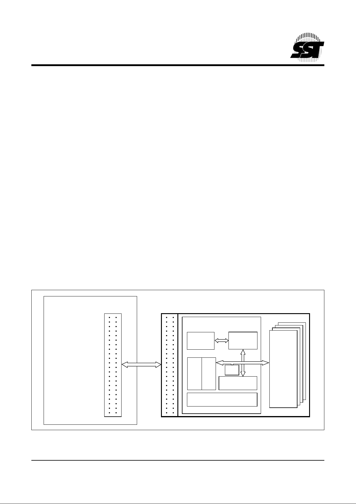
1.0 GENERAL DESCRIPTION
The SST’s ATA-Disk Module (ADM) contains a controller,
embedded firmware, and Flash Media with a 40-pin or 44pin female connector. Refer to Figure 1-1 for SST’s ADM
block diagram. The controller interfaces with th e host system allowing data to b e w ritten to and rea d f ro m the Fla s h
Media.
1.1 Perf ormance-optimized AT A Contr oller
The heart of the ADM is the A TA controller which translates
standard ATA signals into Flash Media d ata and contro ls.
SST’s ADM contains a p roprietary ATA controller sp ecifically designed to attain high d ata throughpu t from host t o
Flash. The following components contribute to the A T A controller’s performance.
1.1.1 Microcontroller Unit (MCU)
The MCU translates ATA co mmands in to data an d control
signals required for flash memory operation.
1.1.2 Internal Direct Memory Access (DMA)
The ATA controller inside ADM uses DMA allowing i nstan t
data transfer from buffer to memory. This implementation
eliminates microc ontroller overhead associated with traditional, firmware based, memory control, increasing data
transfer rate.
1.1.3 Power Management Unit (PMU)
Power Management Unit controls the power c onsumptio n
of the ADM. The PMU dramatically extends product battery
life by putting the part of the circuitry that is not in operation
into sleep mode.
1.1.4 SRAM Buffer
A key contributor to the ATA contro ller performance is an
SRAM buffer. The buffer optimizes the data writes to Flash.
1.1.5 Embedded Flash File System
Embedded Flash File System is an integral part of the
SST’s ATM controll er. It contains MCU Fir mware that performs the f ollow ing tasks:
1. Translates host side signals into Flash Media
Writes and Reads.
2. Provides Flash Media wear leveling to spread the
Flash writes across all the memory address space
to increase the longevity of Flash Media.
3. Keeps track of data file structures.
1.1.6 Error Correction
The ATA Controller contains ECC algorithm that corrects 3
bytes of error per 512 Byte sector.
FIGURE 1-1: SST ATA-D
ISK MODULE BLOCK DIAGRAM
519 ILL1-1.4
40 or 44-Pin
Male IDE Connector
40 or 44-Pin
Female IDE Connector
PC
Mother
Board
ATA Controller
Flash
Media
Embedded
Flash
File System
MCU
ECC
Internal
DMA
SRAM Buffer
PMU
ATA-Disk Module
Page 6
6
Advance Information
ATA-Disk Module
SST58SM008 / 016 / 024 / 032 / 048 / 064 / 096 / 128 / 192
SST58LM008 / 016 / 024 / 032 / 048 / 064 / 096 / 128 / 192
©2001 Silicon Storage Technology, Inc. S71193-01-000 9/01 519
1.2 SST’s ATA-Disk Module Product Offering
The SST58SM/LMxx x ATA-Disk Module produc t family is available in 8 to 192 MB yte den si tie s. The following table
shows the specific capacity, default number of cylinder heads, sectors and cylinders for each product line.
2.0 ELECTRICAL INTERFACE
2.0.1 Pin Assignment and Pin Type
The signal/pin assignme nts are listed in Tables 2- 1 and 2-2. Low active signals have a “#” suffix. Pin types are
Input, Output or Input/Output. Section 2.3 defines the DC characteristics for all input and output type structures.
2.1 Electrical Description
The ADM functions in ATA Mode, which is compatible with IDE hard disk drives.
Table 2-3 describe s the I/O si gnals. Signals whose sourc e is the h ost are desi gnated as i nputs while s ignals that
the ADM sources are outputs. All outputs from the ADM are totem pole except the data bus signals which are in the
bi-directional tri-state. Refer to Section 2.3.2 for definitions of Input and Output types.
Model Number Density T ota l Bytes Cylinders Heads Sectors
SST58SM/LM008 8 MB 8,028,160 245 2 32
SST58SM/LM016 16 MB 16,023,552 489 2 32
SST58SM/LM024 24 MB 24,051,712 367 4 32
SST58SM/LM032 32 MB 32,047,104 489 4 32
SST58SM/LM048 48 MB 48,037,888 733 4 32
SST58SM/LM064 64 MB 64,028,672 977 4 32
SST58SM/LM096 96 MB 96,075,776 733 8 32
SST58SM/LM128 128 MB 128,057 ,344 977 8 32
SST58SM/LM192 192 MB 192,151 ,552 733 16 32
Page 7
Advance Information
ATA-Disk Module
SST58SM008 / 016 / 024 / 032 / 048 / 064 / 096 / 128 / 192
SST58LM008 / 016 / 024 / 032 / 048 / 064 / 096 / 128 / 192
7
©2001 Silicon Storage Technology, Inc. S71193-01-000 9/01 519
TABLE 2-1: 44-PIN PIN ASSIGNMENT
Pin No. Signal Name Pin Type I/O Type
1
1 RESET# I I4U
2 GND Ground
3 D7 I/O I2D, O2
4 D8 I/O I2D, O2
5 D6 I/O I2D, O2
6 D9 I/O I2D, O2
7 D5 I/O I2D, O2
8 D10 I/O I2D, O2
9 D4 I/O I2D, O2
10 D11 I/O I2D, O2
11 D3 I/O I2D, O2
12 D12 I/O I2D, O2
13 D2 I/O I2D, O2
14 D13 I/O I2D, O2
15 D1 I/O I2D, O2
16 D14 I/O I2D, O2
17 D0 I/O I2D, O2
18 D15 I/O I2D, O2
19 GND Ground
20 NC
21 NC
22 GND Ground
23 IOWR# I I3U
24 GND Ground
25 IORD# I I3U
26 GND Ground
27 NC
28 NC
2
29 NC
30 NC/WP#
3
I2U
31 INTRQ O O1
32 IOCS16# O O2
33 A1 I I2D
34 PDIAG# I/O I2U, O1
35 A0 I I2D
36 A2 I I2D
37 CS1FX# I I3U
38 CS3FX# I I3U
39 DASP# I/O I2U, O1
40 GND Ground
41 V
DD
Power
42 V
DD
Power
43 GND Ground
44 NC
T2-1.6 519
1. Please refer to Sections 2.3.1 to 2.3.4 for detail
2. Pin 28 is CSEL in standard host 40- pin IDE int erf ace. Master /
Slave setting i s selected t hrough an on-bo ard jumper.
3. Pin 30 is jumper selectable as NC or WP#.
TABLE 2-2: 40-PIN PIN ASSIGNMENT
Pin No. Signal Name Pin Type I/O Type
1
1 RESET# I I4U
2 GND Ground
3 D7 I/O I2D, O2
4 D8 I/O I2D, O2
5 D6 I/O I2D, O2
6 D9 I/O I2D, O2
7 D5 I/O I2D, O2
8 D10 I/O I2D, O2
9 D4 I/O I2D, O2
10 D11 I/O I2D, O2
11 D3 I/O I2D, O2
12 D12 I/O I2D, O2
13 D2 I/O I2D, O2
14 D13 I/O I2D, O2
15 D1 I/O I2D, O2
16 D14 I/O I2D, O2
17 D0 I/O I2D, O2
18 D15 I/O I2D, O2
19 GND Ground
20 V
DD
2
Power
21 NC
22 GND Ground
23 IOWR# I I3U
24 GND Ground
25 IORD# I I3U
26 GND Ground
27 NC
28 NC
3
29 NC
30 NC/WP#
4
I2U
31 INTRQ O O1
32 IOCS16# O O2
33 A1 I I2D
34 PDIAG# I/O I2U, O1
35 A0 I I2D
36 A2 I I2D
37 CS1FX# I I3U
38 CS3FX# I I3U
39 DASP# I/O I2U, O1
40 GND Ground
T2-2.6 519
1. Please refer to Sections 2.3.1 to 2.3.4 for detail.
2. Optional, not av ai lab le in sta ndard host 40 -pin IDE interf a ce.
3. Pin 28 is CSEL in standard host 40- pin IDE int erf ace. Master /
Slave setting i s selected t hrough an on-bo ard jumper.
4. Pin 30 is jumper selectable as NC or WP#.
Page 8
8
Advance Information
ATA-Disk Module
SST58SM008 / 016 / 024 / 032 / 048 / 064 / 096 / 128 / 192
SST58LM008 / 016 / 024 / 032 / 048 / 064 / 096 / 128 / 192
©2001 Silicon Storage Technology, Inc. S71193-01-000 9/01 519
For the 40-pin ATA-Disk Module, power can be supplied either through the pin 20 (not presen t on standard 40- pin
IDE interface) or through the external power connector provided on the 40- pin ADM. Please see the drawings in
“Physical Dimensions” on page 36 for information.
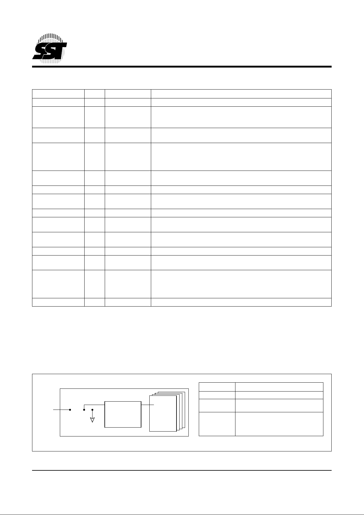
FIGURE 2-1: P
IN 30 CONFIGURATION
TABLE 2-3: SIGNAL DESCRIPTION
Symbol Type1Pin Name and Functions
A2 - A0 I 33,34,35 A[2:0] are used to select one of the Task File registers.
D15 - D0 I/O 18,16,14,12,10,
8,6,4,3,5,7,9,11,
13,15,17
Data bus
CS1FX#, CS3FX# I 37,38 CS1FX# is the chip select for the task file registers while CS3FX# is used to
select the Alternate Status Register and the Device Control Register.
CSEL - 28 CSEL signal is a NC to the motherboard. The Master/Slave selection is set by a
jumper. If the jumper is in a Master position, the ADM is addressed as a Master
drive, and if the jumper is in a Slave position, the ADM is addressed as a Slave
drive.
IORD# I 25 This is an I/O Read st robe gener ated b y the host. This signa l gates I/O data
onto the bus from the chip.
IOWR# I 23 The I/O Write strobe pulse is used to clock I/O data into the chip.
IOCS16# O 32 This output signal is asserted low when this dev ice is e xp ecting a w ord data
transfer cy cl e .
INTRQ O 31 Signal is the active high Interrupt Request to the host.
PDIAG# I/O 34 This input/output is the Pass Diagnostic signal in the Master/Slave hand-
shake protocol.
DASP# I/O 39 This inp ut/output is the Disk Activ e/Sla v e present sign al in the Maste r/Slav e
handshake prot oco l.
RESET# I 1 This input pin is the active low hardware reset from the host.
GND - 2,19,22,24,26,
30,40,43
2
Ground
WP#
3
I 30 Write protect pin is used to disable Write operation. The 3-position jumper can set
pin 30 as NC, write protected (by connecting to GND), or host selectable (by connecting to pin 30 of IDE connector). When the signal on this pin is low , data on the
chip will be write-protected. (See Figure 2-1)
V
DD
-204, 412, 42
2
Power
T2-3.6 519
1. Please refer to Sections 2.3.1 to 2.3.4 for detail
2. Only available with the 44-pin connector module
3. Pin 30 is jumper selectable as NC or WP#
4. Only available with the 40-pin connector module
519 ILL2-5.1
ATA Controller
Flash
Memory
231
Pin 30
WP# Jumper
ATA-Disk Module
WP# Jumper A TA-Disk Module
No Jumper NC, Module is NOT write protected.
Close 1, 2 Connect to Ground,
Module is write protected
Close 2, 3 Host Selectable,
Module is write protected if pin 30 is low.
Module is NOT write protected if pin 30
is high.
T2-3.0 519
Page 9

Advance Information
ATA-Disk Module
SST58SM008 / 016 / 024 / 032 / 048 / 064 / 096 / 128 / 192
SST58LM008 / 016 / 024 / 032 / 048 / 064 / 096 / 128 / 192
9
©2001 Silicon Storage Technology, Inc. S71193-01-000 9/01 519
2.2 Absolute Maximum Stress Ratings
Absolute Maximum Stress Ratings (Applied conditions greater than those listed under “Absolute Maximum
Stress Ratings” may cause pe r manent dama ge to the device. This i s a stress rating only an d funct ional operatio n
of the device at these conditions or conditions greater tha n those defined in the ope rational sections of this data
sheet is not implied. Exposure to absolute maximum stress rating conditions may affect device reliability.)
Temperature Under Bias . . . . . . . . . . . . . . . . . . . . . . . . . . . . . . . . . . . . . . . . . . . . . . . . . . . . . . . . . -55°C to +125°C
Storage Temperature . . . . . . . . . . . . . . . . . . . . . . . . . . . . . . . . . . . . . . . . . . . . . . . . . . . . . . . . . . . . -50°C to +100°C
D.C. Voltage on any Pin to Ground Potential . . . . . . . . . . . . . . . . . . . . . . . . . . . . . . . . . . . . . . . . .-0.5V to V
DD
+0.5V
Transient Voltage (<20 ns) on Any Pin to Ground Potential. . . . . . . . . . . . . . . . . . . . . . . . . . . . . .-1.0V to V
DD
+1.0V
Package Power Dissipation Capability (Ta = 25°C) . . . . . . . . . . . . . . . . . . . . . . . . . . . . . . . . . . . . . . . . . . . . . . 1.0W
Through Hole Lead Soldering Temperature (10 Seconds). . . . . . . . . . . . . . . . . . . . . . . . . . . . . . . . . . . . . . . . 300° C
Surface Mount Lead Soldering Temperature (3 Seconds). . . . . . . . . . . . . . . . . . . . . . . . . . . . . . . . . . . . . . . . 240° C
Output Short Circ uit Curr ent
1
. . . . . . . . . . . . . . . . . . . . . . . . . . . . . . . . . . . . . . . . . . . . . . . . . . . . . . . . . . . . . 50 mA
1. Outputs shorted for no more than one second. No more than one output shorted at a time.
OPERATING RANGE: SST58SMXXX
Range Ambient Temp V
DD
Commercia l 0°C to +70°C 4.5-5.5V
OPERATING RANGE: SST58LMXXX
Range Ambient Temp V
DD
Commercial 0°C to +70°C 3.135-3.465V
AC CONDITIONS OF TEST
Input Rise/Fall Time . . . . . . . . . . . . . . 10 ns
Output Load . . . . . . . . . . . . . . . . . . . . C
L
= 100 pF
See Figure 2-3
Note: All AC specifications are guaranteed by design.
TABLE 2-4: RECOMMENDED SYSTEM POWER-UP TIMINGS
Symbol Parameter Maximum Units
T
PU-READY
1
1. This parameter is measured only for initial qualification and after a design or process change that could affect this parameter.
Power-up to Ready Operation 500 ms
T
PU-WRITE
1
Power-up to Program/Erase Operation 500 ms
T2-4.0 519
Page 10
10
Advance Information
ATA-Disk Module
SST58SM008 / 016 / 024 / 032 / 048 / 064 / 096 / 128 / 192
SST58LM008 / 016 / 024 / 032 / 048 / 064 / 096 / 128 / 192
©2001 Silicon Storage Technology, Inc. S71193-01-000 9/01 519
2.3 Electrical Specification
The following tables define all D.C. Characteristics for the SST ATA-Disk Module product family.
2.3.1 Absolute Maximum Conditions
Unless otherwise stated, conditions are for Commercial Temperature:
Non-operating (storage) temperature range: -50°C to +100°C
V
DD
= 4.5-5.5V
V
DD
= 3.135-3.465V
Ta = 0°C to +70°C
ADM products shall operate correctly in both voltage ranges as shown in the tables above. To comply with th is
specification, current requirements must not exceed the maximum limit.
2.3.2 Input Leakage Current
In the table below, x refers to the characteristics descr ibed in Sectio n 2.3.2. For example, I1U indicates a pul l up
resistor with a type 1 input characteristic.
A
BSOLUTE MAXIMUM CONDITIONS
Parameter Symbol Conditions
Input Powe r V
DD
-0.3V min to 6.5V max
Voltage on any pin except V
DD
with respect to GND V -0.5V min to VDD + 0.5V max
INPUT POWER
Voltage
Maximum Average RMS
Active Current
Maximum Average RMS
Sleep Current Measurement Method
3.135-3.465V 75 mA 200 µA 3.3V at 25
°C
1
1. Current measurement is accomplished by connecting an amp meter (set to the 2 amp scale range) in series with the VDD supply to
the ADM. Current measurements are to be taken while looping on a data transfer command with a sector count of 128. Current consumption values for both Read and Write commands are not to exceed the Maximum Average RMS Current specified in the above
table.
4.5-5.5V 100 mA 300 µA 5.0V at 25°C
1
Type Parameter Symbol Conditions MIN TYP MAX Units
IxZ Input Leakage Current IL V
IH
= VDD / VIL = Gnd -1 1 µA
IxU Pull Up Resistor RPU1 VDD = 5.0V 50k 500k Ohm
IxD Pull Down Resistor RPD1 VDD = 5.0V 50k 500k Ohm
Page 11
Advance Information
ATA-Disk Module
SST58SM008 / 016 / 024 / 032 / 048 / 064 / 096 / 128 / 192
SST58LM008 / 016 / 024 / 032 / 048 / 064 / 096 / 128 / 192
11
©2001 Silicon Storage Technology, Inc. S71193-01-000 9/01 519
2.3.3 Input Characteristics
2.3.4 Output Drive Type
All output drive type are CMOS level.
2.3.5 Output Drive Characteristics
Type Parameter Symbol
Min Typ Max Min Typ Max
UnitsVDD = 3.3V VDD = 5.0V
1 Input Voltage V
IH
2.4 2.4 Volts
CMOS V
IL
0.6 0.8
2 Input Voltage V
IH
2.0 2.7 Volts
CMOS V
IL
0.8 0.8
3 Input Voltage V
TH
2.0 2.4 Volts
CMOS V
TL
0.5 0.8
Schmitt Trigger
4 Input Voltage V
TH
1.8 2.4 Volts
CMOS V
TL
0.9 0.8
Schmitt Trigger
Type Parameter Symbol Conditions MIN TYP MAX Units
O1 Output Voltage V
OH
IOH = -4 mA VDD-0.8V Volts
V
OL
IOL = 4 mA Gnd+0.4V
O2 Output Voltage V
OH
IOH = -8 mA VDD-0.8V Volts
V
OL
IOL = 8 mA Gnd+0.4V
Page 12
12
Advance Information
ATA-Disk Module
SST58SM008 / 016 / 024 / 032 / 048 / 064 / 096 / 128 / 192
SST58LM008 / 016 / 024 / 032 / 048 / 064 / 096 / 128 / 192
©2001 Silicon Storage Technology, Inc. S71193-01-000 9/01 519
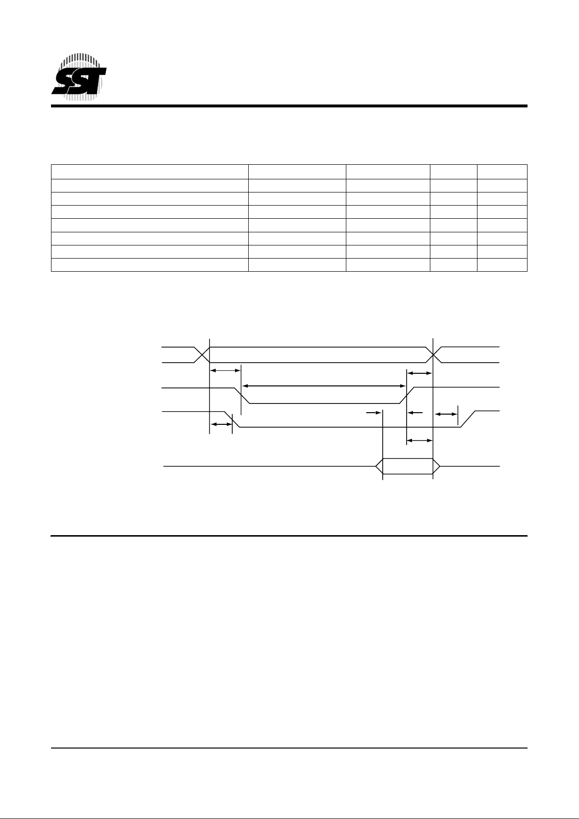
2.3.6 I/O Input (Read) Timing Specification
Note: All times are in nanoseconds. The maximum load on IOCS16# is 1 LSTTL with 50pF total load.
All AC specifications are guaranteed by design.
FIGURE 1: I/O READ TIMING DIAGRAM
TABLE 2-5: I/O READ TIMING
Item Symbol IEEE Symbol Min Max
Data Setup before IORD# tsu(IORD) tDVIRH 20 Data Hold following IORD# th(IORD) tlGHQX 5 IORD# Width Time tw(IORD) tlGLIGH 70 Valid Address Setup before IORD# tsuA(IORD) tAVIGL 25 Valid Address Hold following IORD# thA(IORD) tlGHAX 10 IOCS16# Delay Falling from Address tdfIOCS16(ADR) tAVISL - 20
IOCS16# Delay Rising from Address tdrIOCS16(ADR) tAVISH 20
T2-5.4 519
519 ILL2-7.3
tdrIOCS16(ADR)
tdfIOCS16(ADR)
thA(IORD)
th(IORD)
tsuA(IORD)
tsu (IORD)
tw(IORD)
Valid Address
1
IORD#
IOCS16#
D15-D0
Dout
1. Valid Address consists of signals CS1FX#, CS3FX#, and A2-A0.
Page 13

Advance Information
ATA-Disk Module
SST58SM008 / 016 / 024 / 032 / 048 / 064 / 096 / 128 / 192
SST58LM008 / 016 / 024 / 032 / 048 / 064 / 096 / 128 / 192
13
©2001 Silicon Storage Technology, Inc. S71193-01-000 9/01 519
2.3.7 I/O Output (Write) Timing Specification
Note: All times are in nanoseconds. The maximum load on IOCS16# is 1 LSTTL with 50pF total load.
All AC specifications are guaranteed by design.
FIGURE 2-2: I/O WRITE TIMING DIAGRAM
FIGURE 2-3: AC INPUT/OUTPUT REFERENCE WAVEFORMS
TABLE 2-6: I/O WRITE TIMING
Item Symbol IEEE Symbol Min Max
Data Setup before IOWR# tsu(IOWR) tDVIWH 20 Data Hold following IOWR# th(IOWR) tlWHDX 10 IOWR# Width Time tw(IOWR) tlWLIWH 70 Valid Address Setup before IOWR# tsuA(IOWR) tAVIWL 25 Valid Address Hold following IOWR# thA(IOWR) tlWHAX 10 IOCS16# Delay Falling from Address tdfIOCS16(ADR) tAVISL - 20
IOCS16# Delay Rising from Address tdrIOCS16(ADR) tAVISH 20
T2-6.4 519
519 ILL2-8.4
tdrIOCS16(ADR)
tdfIOCS16(ADR)
thA(IOWR)
th(IOWR)tsu(IOWR)
Din Valid
tsuA(IOWR)
tw(IOWR)
Valid Address
1
IORW#
IOCS16#
D15-D0
1. Valid Address consists of signals CS1FX#, CS3FX#, and A2-A0.
519 ILL F11.0
REFERENCE POINTS OUTPUTINPUT
V
HT
V
LT
V
HT
V
LT
V
IHT
V
ILT
AC test inputs are driven at V
IHT
(2.4V) for a logic “1” and V
IL T
(0.4V) for a logic “0”. Measu rement reference points for
inputs and outputs are V
HT
(2.0V) and VLT (0.8V). Input rise and fall times (10% ↔ 90%) are <10 ns.
Note: V
HT
- V
HIGH
Test
V
LT
- V
LOW
Test
V
IHT
- V
INPUT
HIGH Test
V
ILT
- V
INPUT
LOW Test
Page 14

14
Advance Information
ATA-Disk Module
SST58SM008 / 016 / 024 / 032 / 048 / 064 / 096 / 128 / 192
SST58LM008 / 016 / 024 / 032 / 048 / 064 / 096 / 128 / 192
©2001 Silicon Storage Technology, Inc. S71193-01-000 9/01 519
2.4 I/O Transfer Function
2.4.1 I/O Function
ADM permits 8-bit data access if the user issues a Set Feature Command to enable 8-bit Mode.
The following table defines the function of various operations.
TABLE 2-7: I/O F
UNCTION
Function Code CS3FX# CS1FX# A0-A2 IORD# IOWR# D15-D8 D7-D0
Invalid Mode V
IL
V
IL
X
1
1. X can be VIL or VIH, but no other value.
X X Undefined Undefined
Standby Mode V
IH
V
IH
X X X High Z High Z
Task File Write V
IH
V
IL
1-7H V
IH
V
IL
XData In
Task File Read V
IH
V
IL
1-7H V
IL
V
IH
High Z Data Out
Data Register Write V
IH
V
IL
0VIHV
IL
In
2
2. If 8-bit data transfer mode is enabled.
In 8-bit data transfer mode, High Byte is undefined for Data Out, can be V
IL
or VIH, but no other value, for Data In.
In
Data Register Read V
IH
V
IL
0VILV
IH
Out
2
Out
Control Register Write V
IL
V
IH
6H V
IH
V
IL
X Control In
Alt Status Read V
IL
V
IH
6H V
IL
V
IH
High Z Status Out
Drive Address V
IL
V
IH
7H V
IL
V
IH
High Z Data Out
T2-7.1 519
Page 15

Advance Information
ATA-Disk Module
SST58SM008 / 016 / 024 / 032 / 048 / 064 / 096 / 128 / 192
SST58LM008 / 016 / 024 / 032 / 048 / 064 / 096 / 128 / 192
15
©2001 Silicon Storage Technology, Inc. S71193-01-000 9/01 519
3.0 SOFTWARE INTERFACE
3.1 ATA-Disk Module Drive Register Set Definitions and Protocol
3.1.1 ATA-Disk Module Addressing
The I/O decoding for an ADM is as follows:
3.1.2 ATA-Disk Module Registers
The following section describes the hardware r eg ister s u sed by the h ost s oftware to is sue commands to the ADM .
These registers are often collectively referred to as the “Task File Registers.”
3.1.2.1 Data Register
This 16-bit register is used to transfer data blocks between the device data buffer and the host. It is also the register
through which sector infor mation is transferred on a Format Track command. Data transfer can be performed in
PIO mode.
3.1.2.2 Error Register (Read Only)
This register co ntains a dditional i nformatio n about th e sou rce of an error wh en an er ror is indicat ed in bit 0 of th e
Status register. The bits are defined as follows:
Bit 7 (BBK) This bit is set when a Bad Block is detected.
Bit 6 (UNC) This bit is set when an Uncorrectable Error is encountered.
Bit 5 This bit is 0.
Bit 4 (IDNF) The requested sector ID is in error or cannot be found.
Bit 3 This bit is 0.
Bit 2 (Abort) This bit is set if the command has been abor ted because of an ADM status condi tion:
(Not Ready, Write Fault, etc.) or when an invalid command has been issued.
Bit 1 This bit is 0.
Bit 0 (AMNF) This bit is set in case of a general error.
TABLE 3-1: T
ASK REGISTERS
CS3FX# CS1FX# A2 A1 A0 IORD# = 0 IOWR# = 0
1 0 0 0 0 RD Data WR Data
1 0 0 0 1 Error Register Features
1 0 0 1 0 Sector Count Sector Count
1 0 0 1 1 Sector No. Sector No.
1 0 1 0 0 Cylinder Low Cylinder Low
1 0 1 0 1 Cylinder High Cylinder High
1 0 1 1 0 Select Card/Head Select Card/Head
1 0 1 1 1 Status Command
0 1 1 1 0 Alt Status Device Control
0 1 1 1 1 Drive Address Reserved
T3-1.0 519
D7 D6 D5 D4 D3 D2 D1 D0
BBK UNC 0 IDNF 0 ABRT 0 AMNF
Page 16

16
Advance Information
ATA-Disk Module
SST58SM008 / 016 / 024 / 032 / 048 / 064 / 096 / 128 / 192
SST58LM008 / 016 / 024 / 032 / 048 / 064 / 096 / 128 / 192
©2001 Silicon Storage Technology, Inc. S71193-01-000 9/01 519
3.1.2.3 Fea tur e Regist er (Writ e Only)
This register provides information regarding features of the ADM that the host can utilize.
3.1.2.4 Sector Count Register
This register contain s the numbers of sectors of data requested to be transferred on a Read or Write operation
between the host and the ADM. If the value in this regis ter is zero, a count of 256 secto rs is specifi ed. If the command was successful, this register is zero at command completion. If not successfully completed, the register contains the number of sectors that need to be transferred in order to complete the request.
3.1.2.5 Sector Number (LBA 7-0) Register
This register contains the s tar ting sector number or bits 7-0 of the Logical Block Address (LBA ) for any ADM data
access for the subsequent command.
3.1.2.6 Cy lin der Low (LBA 15-8) Register
This register contains the low order 8 bits of the starting cylinder address or bits 15-8 of then Logical Block
Address.
3.1.2.7 Cylinder High (LBA 23-16) Register
This register contains the high order bits of the starting cylinder address or bits 23-16 of the Logical Block Address.
3.1.2.8 Drive/Head (LBA 27-24) Register
The Drive/Head register is used to sele ct the drive and h ead. It is also us ed to select LB A addressing in stead of
cylinder/head/sector addressing. The bits are defined as follows:
Bit 7 This bit is set to 1.
Bit 6 LBA is a flag to select either Cylinder/Head/Sector (CHS) or Logical Block Address
Mode (LBA). When LBA=0, Cylinder/Head/Sector mode is selected. When LBA=1,
Logical Block Address is selected. In L ogical Block Mode, the Logic al Block Address is
interpreted as follows:
LBA7-LBA0: Sector Number Register D7-D0.
LBA15-LBA8: Cylinder Low Register D7-D0.
LBA23-LBA16: Cylinder High Register D7-D0.
LBA27-LBA24: Drive/Head Register bits HS3-HS0.
Bit 5 This bit is set to 1.
Bit 4 (DRV) DRV is the drive number. When DRV=0 (Master), Master is selected.
When DRV=1(Slave), Slave is selected.
Bit 3 (HS3) When operating in the Cylinder, Head, Sector mode, this is bit 3 of the head number.
It is Bit 27 in the Logical Block Address mode.
Bit 2 (HS2) When operating in the Cylinder, Head, Sector mode, this is bit 2 of the head number.
It is Bit 26 in the Logical Block Address mode.
Bit 1 (HS1 When operating in the Cylinder, Head, Sector mode, this is bit 1 of the head number.
It is Bit 25 in the Logical Block Address mode.
Bit 0 (HS0) When operating in the Cylinder, Head, Sector mode, this is bit 0 of the head number.
It is Bit 24 in the Logical Block Address mode.
D7 D6 D5 D4 D3 D2 D1 D0
1LBA1
DRV HS3 HS2 HS1 HS0
Page 17

Advance Information
ATA-Disk Module
SST58SM008 / 016 / 024 / 032 / 048 / 064 / 096 / 128 / 192
SST58LM008 / 016 / 024 / 032 / 048 / 064 / 096 / 128 / 192
17
©2001 Silicon Storage Technology, Inc. S71193-01-000 9/01 519
3.1.2.9 Status & Alternate Status Registers (Read Only)
These register s return the ADM st atus when re ad b y the ho st. R eadi ng the St atus regist er does clea r a pend ing in terrupt while reading the Auxiliary Status register does not. The meaning of the status bits are described as follows:
Bit 7 (BUSY) The busy bit is set whe n the ADM has a ccess to the c ommand buffer and regist ers and
the host is locked out from accessing the command re gister and buffer. No other bits in
this register are valid when this bit is set to a 1.
Bit 6 (RDY) RDY indicates whether the device is capable of performing ADM op erations. This bit is
cleared at power up and remains cleared until the ADM is ready to accept a command.
Bit 5 (DWF) This bit, if set, indicates a write fault has occurred.
Bit 4 (DSC) This bit is set when the ADM is ready.
Bit 3 (DRQ) The Data Request is set when the ADM requires that information be transferred either to
or from the host through the Data register.
Bit 2 (CORR) This bit is se t when a Correctable data error has been e ncountered and the data has
been corrected. This condition does not terminate a multi-sector Read operation.
Bit 1 (IDX) This bit is always set to 0.
Bit 0 (ERR) This bit is set when the previous com mand has end ed in some type of er ror. The bits in
the Error register contai n additional information desc ribing the error. It is recommended
that media access commands (such as Read Sect ors and Write Sectors) tha t end with
an error condition should have the address of the first sect or in error in the command
block registers.
3.1.2.10 Device Control Register (Write Only)
This register is used to c ontrol the A DM inter rup t reque st and to i ssue a software Reset. This register can be written to even if the device is BUSY. The bits are defined as follows:
Bit 7 This bit is an X (don’t care).
Bit 6 This bit is an X (don’t care).
Bit 5 This bit is an X (don’t care).
Bit 4 This bit is an X (don’t care).
Bit 3 This bit is ignored by the ADM.
Bit 2 (SW Rst)This bi t is set to 1 in or der to force the ADM to perform a software R eset op eration. Th e
chip remains in Reset until this bit is reset to ‘0.’
Bit 1 (-IEn) The Interrupt Enable bit enables interrupts when the bit is 0. When the bit is 1, interrupts
from the ADM are disabled. This bit is Reset to 0 at power on and Reset.
Bit 0 This bit is ignored by the ADM.
D7 D6 D5 D4 D3 D2 D1 D0
BUSY RD Y DWF
DSC DRQ CORR 0 ERR
D7 D6 D5 D4 D3 D2 D1 D0
XXX
X1SW Rst-IEn0
Page 18

18
Advance Information
ATA-Disk Module
SST58SM008 / 016 / 024 / 032 / 048 / 064 / 096 / 128 / 192
SST58LM008 / 016 / 024 / 032 / 048 / 064 / 096 / 128 / 192
©2001 Silicon Storage Technology, Inc. S71193-01-000 9/01 519
3.1.2.11 Drive Address Register (Read Only)
This register con tains the i nverted dr ive select and h ead s elect addr esses o f th e curr ently select ed drive. The b its
in this register are as follows:
Bit 7 This bit is HiZ.
Bit 6 (-WTG) This bit is 0 when a Write operation is in progress, otherwise, it is 1.
Bit 5 (-HS3) This bit is the negation of bit 3 in the Drive/Head register.
Bit 4 (-HS2) This bit is the negation of bit 2 in the Drive/Head register.
Bit 3 (-HS1) This bit is the negation of bit 1 in the Drive/Head register.
Bit 2 (-HS0 This bit is the negation of bit 0 in the Drive/Head register.
Bit 1 (-DS1) This bit is 0 when drive 1 is active and selected.
Bit 0 (-DS0) This bit is 0 when drive 0 is active and selected.
3.1.2.12 Command Register (Write Only)
This register cont ains the command code b eing sent to the dr ive. Command execution begins immediately after
this register is wr itten. The executable commands, the command codes, an d the necessar y parameters for each
command are listed in Table 3-2.
D7 D6 D5 D4 D3 D2 D1 D0
HiZ -WTG -HS3 -HS2 -HS1 -HS0 -DS1 -DS0
Page 19

Advance Information
ATA-Disk Module
SST58SM008 / 016 / 024 / 032 / 048 / 064 / 096 / 128 / 192
SST58LM008 / 016 / 024 / 032 / 048 / 064 / 096 / 128 / 192
19
©2001 Silicon Storage Technology, Inc. S71193-01-000 9/01 519
3.2 ATA-Disk Module Command Description
This section defines the software requirements and the format of the commands the host sends to the ADM. Commands are issued to the ADM by loading the requir ed registers in the command block with the suppl ied parameters, and then writing the command code to the Command Register. The manner in which a command is accepted
varies. There are three clas ses (see Table 3-2) o f command acceptance, all depende nt on the host not issuing
commands unless the ADM is not busy (BSY=0).
3.2.1 ATA-Disk Module Command Set
Table 3-2 su mmar izes the A DM com mand s et with th e paragraphs tha t follow describ ing the i ndivid ual co mmands
and the task file for each.
TABLE 3-2: ATA-D
ISK MODULE COMMAND SET
Class Command Code FR
1
1. FR - Features Register
SC
2
2. SC - Sector Count Register
SN
3
3. SN - Sector Number Register
CY
4
4. CY - Cylinder Registers
DH
5
5. DH - Drive/Head Register
LBA
6
6. LBA - Logical Block Address Mode Supported (see command descriptions for use)
1 Check Power Mode E5H or 98H - - - - D
8
1 Execute Drive Diagnostic 90H - - - - D 2 Format Track 50H - Y
7
7. Y - The register contains a valid parameter for this command.
-YY
8
8. For the Drive/Head Register: Y means both the ADC and Head parameters are used;
D means only the ADC parameter is valid and not the Head parameter.
Y
1 Identify Drive ECH - - - - D 1 Idle E3H or 97H - Y - - D 1 Idle Immediate E1H or 95H - - - - D 1 Initialize Drive Parameters 91H - Y - - Y 1 Read Buffer E4H - - - - D 1 Read Long Sector 22H or 23H - - Y Y Y Y
1Read Multiple C4H -YYYY Y
1Read Sector(s) 20H or 21H -YYYY Y
1Read Verify Sector(s) 40H or 41H -YYYY Y
1 Recalibrate 1XH - - - - D 1Seek 7XH - -YYY Y
1 Set Features EFH Y - - - D 1 Set Multiple Mode C6H - Y - - D 1 Set Sleep Mode E6H or 99H - - - - D 1 Stand By E2H or 96H - - - - D 1 Stand By Immediate E0H or 94H - - - - D 2 Write Buffer E8H - - - - D 2 Write Long Sector 32H or 33H - - Y Y Y Y
3Write Multiple C5H -YYYY Y
2Write Sector(s) 30H or 31H -YYYY Y
3Write Verify 3CH -YYYY Y
T3-2.0 519
Page 20

20
Advance Information
ATA-Disk Module
SST58SM008 / 016 / 024 / 032 / 048 / 064 / 096 / 128 / 192
SST58LM008 / 016 / 024 / 032 / 048 / 064 / 096 / 128 / 192
©2001 Silicon Storage Technology, Inc. S71193-01-000 9/01 519
3.2.1.1 Ch eck Power Mode - 98H or E5H
This command checks the power mode.
Because SST ADM can recover from sleep in 200 ns, Idle Mode is never enabled.
ADM sets BSY, sets the Sector Count Register to 00H, clears BSY and generates an interrupt.
3.2.1.2 Execute Drive Diagnostic - 90H
This command performs the internal diagnostic tests implemented by the ADM.
If the Drive bit is ignored and the diagnosti c command is executed by both the Master and the Slave
with the Master responding wi th status for both devices.
The Diagnostic codes shown in Table 3-3 are returned in the Error Register at the end of the command.
Bit ->76543210
Command (7)
98H or E5H
C/D/H (6)
XDrive X
Cyl High (5)
X
Cyl Low (4)
X
Sec Num (3)
X
Sec Cnt (2)
X
Feature (1)
X
Bit ->76543210
Command (7)
90H
C/D/H (6)
XDrive X
Cyl High (5)
X
Cyl Low (4)
X
Sec Num (3)
X
Sec Cnt (2)
X
Feature (1)
X
TABLE 3-3: DIAGNOSTIC CODES
Code Error Type
01H No Error Detected
02H Formatter Device Error
03H Sector Buffer Error
04H ECC Circuitry Error
05H Controlling Microprocessor Error
8XH Slave Error
T3-3.0 519
Page 21

Advance Information
ATA-Disk Module
SST58SM008 / 016 / 024 / 032 / 048 / 064 / 096 / 128 / 192
SST58LM008 / 016 / 024 / 032 / 048 / 064 / 096 / 128 / 192
21
©2001 Silicon Storage Technology, Inc. S71193-01-000 9/01 519
3.2.1.3 Forma t Track - 50H
This command writ es the desired head and cylinder of the selected dr ive with a vendor unique data
pattern (typically FFH or 00H). To remain host backward compatible, the ADM expects a sector buffer of
data from the host to follow the command with th e same protocol as the Write Sector(s) command
although the information i n the buffer is not used by the ADM. If LBA=1 then the number of sect ors to
format is taken from the Sec Cnt register (0=256). The use of this command is not recommended.
3.2.1.4 Identify Drive - ECH
The Identify Drive command enables the host to receive parameter information from the ADM. This
command has the same pro tocol as the Read Se ctor(s) comman d. The parameter words in the buffer
have the arrangement and meanings defined in Table 3-4. All reserved bits or words are zero. Table 3-4
is the definition for each field in the Identify Drive Information.
Bit ->76543210
Command (7)
50H
C/D/H (6)
1 LBA 1 Drive Head (LBA 27-24)
Cyl High (5)
Cylinder High (LBA 23-16)
Cyl Low (4)
Cylinder Low (LBA 15-8)
Sec Num (3)
X (LBA 7-0)
Sec Cnt (2)
Count (LBA mode only)
Feature (1)
X
Bit ->76543210
Command (7)
ECH
C/D/H (6)
XXXDrive X
Cyl High (5)
X
Cyl Low (4)
X
Sec Num (3)
X
Sec Cnt (2)
X
Feature (1)
X
Page 22

22
Advance Information
ATA-Disk Module
SST58SM008 / 016 / 024 / 032 / 048 / 064 / 096 / 128 / 192
SST58LM008 / 016 / 024 / 032 / 048 / 064 / 096 / 128 / 192
©2001 Silicon Storage Technology, Inc. S71193-01-000 9/01 519
TABLE 3-4: IDENTIFY DRIVE INFORMATION
Word
Address
Default
Value
Total
Bytes Data Field Type Information
0 044AH 2 General configuration bit - si gni fic ant information
1 XXXXH 2 Default number of cylinders
2 0000H 2 Reserved
3 00XXH 2 Default number of heads
4 0000H 2 Reserved
5 0000H 2 Reserved
6 XXXXH 2 Default number of sectors per track
7-8 XXXXH 4 Number of sectors per card (Word 7 = MSW, Word 8 = LSW)
9 XXXXH 2 Vendor Unique
10-19 aaaa
1
20 Serial number in ASCII. Big Endian Byte Order in Word
20 0002H 2 Buffer type
21 XXXXH 2 Buffer size in 512 Byte increments
22 0004H 2 # of ECC bytes passed on Read/Write Long Commands
23-26 aaaa
1
8 Firmware revision in ASCII. Big Endian Byte Order in Word
27-46 aaaa
1
40 Model number in ASCII. B ig Endian Byte Order in Word
47 000XH 2 Maximum number of sectors on Read/Write Multiple command
48 0000H 2 Reserved
49 0200H 2 Capabilities
50 0000H 2 Reserved
51 0X00H 2 PIO data transfer cycle timing mode
52 0000H 2 Reserved
53 000XH 2 Transl ati on par am ete rs are valid
54 XXXXH 2 Current numbers of cylinders
55 XXXXH 2 Current numbers of heads
56 XXXXH 2 Current sectors per track
57-58 XXXXH 4 Current capacity in sectors (LBAs) (Word 57 = LSW, Word 58 = MSW)
59 010XH 2 Multiple sector setting
60-61 XXXXH 4 Total number of sectors addressable in LBA Mode
62-63 0000H 4 Reserved (DMA Data Transfer is not supported in ADM)
64 00XXH 2 Advanced PIO Transfer Mode Supported
65-66 0000H 4 Reserved
67 XXXXH 2 Minimum PIO transfer cycle time without flow control
68 XXXXH 2 Minimum PIO transfer cycle time with IORDY flow control
69-127 0000H 138 Reserved
128-159 0000H 64 Vendor unique bytes
160-255 0000H 192 Reserved
T3-4.2 519
1. aaaa - any SST specific number
Page 23

Advance Information
ATA-Disk Module
SST58SM008 / 016 / 024 / 032 / 048 / 064 / 096 / 128 / 192
SST58LM008 / 016 / 024 / 032 / 048 / 064 / 096 / 128 / 192
23
©2001 Silicon Storage Technology, Inc. S71193-01-000 9/01 519
3.2.1.4.1 General Configuration
This field informs th e host tha t this is a non-mag netic, hard se ctored, removable storage device with a
transfer rate greater than 10 MByte/sec and is not MFM encoded.
3.2.1.4.2 Default Number of Cylinders
This field contains th e number of tran slated cylind ers in the default translat ion mode. This value will be
the same as the number of cylinders.
3.2.1.4.3 Default Number of Heads
This field contains the number of translated heads in the default translation mode.
3.2.1.4.4 Default Number of Sectors per Track
This field contains the number of sectors per track in the default translation mode.
3.2.1.4.5 Number of Sectors
This field contains the number of sectors per ADM. This double word value is also the first invalid
address in LBA translation mode.
3.2.1.4.6 Memory Serial Number
The contents of this field are right justified and padded with spaces (20H).
3.2.1.4.7 Buffer Type
This field defines the buffer capability:
0002H: a dual ported multi-sector buffer capable of simultaneous data transfers to or from the host and
the ADM.
3.2.1.4.8 Buffer Size
This field defines the buffer capacity in 51 2 By te inc re men ts. SST’s ADM has up to 2 secto r d ata buffer
for host interface.
3.2.1.4.9 ECC Count
This field defines the number of ECC bytes used on each sector in the Read and Write Long
commands.
3.2.1.4.10 Firmware Revision
This field contains the revision of the firmware for this product.
3.2.1.4.11 Model Number
This field contains the model number for this product and is left justified and padded with spaces (20H).
3.2.1.4.12 Read/Write Multiple Sector Count
This field contains the max imum number of sectors that can be read or written per interr upt using the
Read Multiple or Write Multiple commands.
3.2.1.4.13 Capabilities
Bit 13: Standby Timer Set to 0, forces sleep mode when host is inactive.
Bit 11: IORDY Support Set to 0, indicates that this device may support IORDY operation.
Bit 9: LBA support Set to 1, SST’s ADMs support LBA mode addressing.
Bit 8: DMA Support This bit is set to 0. DMA mode is not supported.
3.2.1.4.14 PIO Data Transfer Cycle Timing Mode
This field defines the mode for PIO data transfer. ADM supports up to PIO Mode-4.
Page 24

24
Advance Information
ATA-Disk Module
SST58SM008 / 016 / 024 / 032 / 048 / 064 / 096 / 128 / 192
SST58LM008 / 016 / 024 / 032 / 048 / 064 / 096 / 128 / 192
©2001 Silicon Storage Technology, Inc. S71193-01-000 9/01 519
3.2.1.4.15 Translation Parameters Valid
If bit 0 is 1, it indicat es that words 54 to 58 are valid and r eflec t the cur rent num ber of cy linde rs, heads
and sectors. If bit 1 is 1, it indicates that words 64 to 70 are valid to support PIO Mode-3 and 4.
3.2.1.4.16 Current Number of Cylinders, Heads, Sectors/Track
These fields contain s the current numb er of user addres sable Cylinders, Heads, and Sec tors/Track in
the current translation mode.
3.2.1.4.17 Current Capacity
This field contains the product of the current cylinders times heads times sectors.
3.2.1.4.18 Multiple Sector Setting
This field contains a validity flag in the Odd Byte and the current number of sectors that can be
transferred per interrupt for R/W Multiple in the Even Byte. The Odd Byte is always 01H which indicates
that the Even Byte is always valid.
The Even Byte value depends on the value set by the Set Multiple comma nd. The Even Byte of this
word by default contains a 00H which indicates that R/W Multiple commands are not valid.
3.2.1.4.19 Total Sectors Addressable in LBA Mode
This field contains the number of sectors addressable for the ADM in LBA mode only.
3.2.1.4.20 Advanced PIO Data Transfer Mode
ADM supports up to PIO Mode-4.
3.2.1.4.21 Minimum PIO Transfer Cycle Time Without Flow Control
The ADM’s minimum cycle time is 120 ns.
3.2.1.4.22 Minimum PIO Transfer Cycle Time with IORDY
The ADM’s minimum cycle time is 120 ns, e.g., PIO Mode-4.
Page 25

Advance Information
ATA-Disk Module
SST58SM008 / 016 / 024 / 032 / 048 / 064 / 096 / 128 / 192
SST58LM008 / 016 / 024 / 032 / 048 / 064 / 096 / 128 / 192
25
©2001 Silicon Storage Technology, Inc. S71193-01-000 9/01 519
3.2.1.5 Idle - 97H or E3H
This command causes the ADM to set BSY, enter the Idle Mode, clear BSY and generate an interrupt. If the
sector count is non-zero, it is interpreted as a timer count with each count being 5 milliseconds and the
automatic power down mode is enabled. If the sector count is zero, the automatic power down mode is also
enabled, the timer count is set to 3, with each count being 5 ms. Note that this time base (5 msec) is different
from the ATA specification.
3.2.1.6 Idle Immediate - 95H or E1H
This command causes the ADM to set BSY, enter the Idle Mode, clear BSY and generate an interrupt.
3.2.1.7 Initialize Drive Parameters - 91H
This command enables the host to set the number of sectors per track and the number of head s per
cylinder. Only the Sector Count and the Drive/Head registers are used by this command.
Bit ->76543210
Command (7)
97H or E3H
C/D/H (6)
XDrive X
Cyl High (5)
X
Cyl Low (4)
X
Sec Num (3)
X
Sec Cnt (2)
Timer Count (5 msec increments)
Feature (1)
X
Bit ->76543210
Command (7)
95H or E1H
C/D/H (6)
XDrive X
Cyl High (5)
X
Cyl Low (4)
X
Sec Num (3)
X
Sec Cnt (2)
X
Feature (1)
X
Bit ->76543210
Command (7)
91H
C/D/H (6)
X 0 X Drive Max Head (no. of heads-1)
Cyl High (5)
X
Cyl Low (4)
X
Sec Num (3)
X
Sec Cnt (2)
Number of Sectors
Feature (1)
X
Page 26

26
Advance Information
ATA-Disk Module
SST58SM008 / 016 / 024 / 032 / 048 / 064 / 096 / 128 / 192
SST58LM008 / 016 / 024 / 032 / 048 / 064 / 096 / 128 / 192
©2001 Silicon Storage Technology, Inc. S71193-01-000 9/01 519
3.2.1.8 Read Buffer - E4H
The Read Buffer command enables t he host to read the curr ent contents of the ADM’s sector buffer.
This command has the same protocol as the Read Sector(s) command
3.2.1.9 Read Multiple - C4H
The Read Multiple command is similar to the Read Sector(s) command. Interrupts are not generated on
every sector, but on the transfer of a block which contains the number of sectors defin ed by a Set
Multiple command.
Command execution is identical to the Read Sectors operation except that the number of sectors
defined by a Set Multip le comma nd are transferred with out int ervening interr upts. DRQ qual ification o f
the transfer is required only at the start of the data block, not on each sector.
The block count of sectors to be transferred witho ut intervening interrup ts is programmed by the Set
Multiple Mode command, which must be executed prior to the Read Multiple command. When the Read
Multiple command is issued, the Sector Count Register contains the number of sectors (not the number
of blocks or the block count) requested. If the number of requested sectors is not evenly divisible by the
block count, as many full blocks as pos sible are transferred, followed by a final, par tial block transfer.
The partial block transfer is for n sectors, where
n = remainder (sector count/block count).
If the Read Multiple command is attempted before the Set Multiple Mode command has been executed
or when Read Multiple commands are disabled, the Read Multiple operation is rejected with an Aborted
Command error. Disk errors encounter ed during Read Multiple c om man ds are pos ted at the beg inning
of the block or partial block transfer, but DRQ is still set and the data transfer will take place as it
normally would, including transfer of corrupted data, if any.
Interrupts are ge nerated when DRQ is set at the beginning of each block or par tial block. The error
reporting is the same as that on a Read Sector(s) Command. This command reads from 1 to 256
sectors as specified in the Sector Count register. A sector count of 0 requests 256 sectors. The transfer
begins at the sector specified in the Sector Number Register.
Bit ->76543210
Command (7)
E4H
C/D/H (6)
XDrive X
Cyl High (5)
X
Cyl Low (4)
X
Sec Num (3)
X
Sec Cnt (2)
X
Feature (1)
X
Bit ->76543210
Command (7)
C4H
C/D/H (6)
1 LBA 1 Drive Head (LBA 27-24)
Cyl High (5)
Cylinder High (LBA 23-16)
Cyl Low (4)
Cylinder Low (LBA 15-8)
Sec Num (3)
Sector Number (LBA 7-0)
Sec Cnt (2)
Sector Count
Feature (1)
X
Page 27

Advance Information
ATA-Disk Module
SST58SM008 / 016 / 024 / 032 / 048 / 064 / 096 / 128 / 192
SST58LM008 / 016 / 024 / 032 / 048 / 064 / 096 / 128 / 192
27
©2001 Silicon Storage Technology, Inc. S71193-01-000 9/01 519
At command compl etion, the C ommand Blo ck Register s con tain t he c ylinder, head and sector number
of the last sector read.
If an error occurs, the r ead terminates at the s ector where the error occurred. The Command Block
Registers contain the cylind er, head and sector number of the sector where the error occurre d. The
flawed data is pending in the sector buffer.
Subsequent blocks or par tial blocks are transferred only if the error was a correctable data error. All
other errors cause the command to stop after transfer of the block which contained the error.
3.2.1.10 Read Long Sector - 22H or 23H
The Read Long command performs similarly to the Read Sector(s) command except that it returns 516
Bytes of data instead of 512 By tes. During a Rea d Long comma nd, the ADM d oes not check the ECC
bytes to determine if there has been a data error. Only single sector read long operations are
support ed. The transfer consists of 512 Bytes of da ta transferred in Word-Mode followed by 4 Bytes o f
ECC data transferred in Byte-Mode. This command has the same protocol as the Read Sector(s)
command. Use of this command is not recommended.
3.2.1.11 Read Sectors - 20H or 21H
This command reads fro m 1 to 256 s ectors as speci fied in th e Sect or Count regis ter. A sector count of
0 requests 256 secto rs. The transfer begins at the sector specified in the S ector Number Register.
When this command is is su ed an d after each sector of data (except the la st one) has been read by the
host, the ADM sets BSY, puts the sector of data in the buffer, sets DRQ, clears BSY, and generates an
interrupt. The host then reads the 512 Bytes of data from the buffer.
At command compl etion, the C ommand Blo ck Register s con tain t he c ylinder, head and sector number
of the last sector read. If an err or occurs, the read termina tes at the sector where the error oc curred.
The Command Block Regis ters con tain the cylinder, head, and sector number of th e secto r where th e
error occurred. The flawed data is pending in the sector buffer.
Bit ->76543210
Command (7)
22H or 23H
C/D/H (6)
1 LBA 1 Drive Head (LBA 27-24)
Cyl High (5)
Cylinder High (LBA 23-16)
Cyl Low (4)
Cylinder Low (LBA 15-8)
Sec Num (3)
Sector Number (LBA 7-0)
Sec Cnt (2)
X
Feature (1)
X
Bit ->76543210
Command (7)
20H or 21H
C/D/H (6)
1 LBA 1 Drive Head (LBA 27-24)
Cyl High (5)
Cylinder High (LBA 23-16)
Cyl Low (4)
Cylinder Low (LBA 15-8)
Sec Num (3)
Sector Number (LBA 7-0)
Sec Cnt (2)
Sector Count
Feature (1)
X
Page 28

28
Advance Information
ATA-Disk Module
SST58SM008 / 016 / 024 / 032 / 048 / 064 / 096 / 128 / 192
SST58LM008 / 016 / 024 / 032 / 048 / 064 / 096 / 128 / 192
©2001 Silicon Storage Technology, Inc. S71193-01-000 9/01 519
3.2.1.12 Read Verify Sector(s) - 40H or 41H
This command is identical to the Read Sectors command, except that DRQ is never set and no data is
transferred to the host. When the command is accepted, the ADM sets BSY.
When the requested sectors have been verified, the ADM clears BSY and generates an interrupt. Upon
command completion, the Command Block Registers contain the cylinder, head, and sector number of the last
sector verified.
If an error occur s, the verify ter minates at the se ctor where th e error occur s. The Command Blo ck Registers
contain the cylinder, head and sector number of the sector where the error occurred. The Sector Count Register
contains the number of sectors not yet verified.
3.2.1.13 R ecal ib rate - 1XH
This command is effectively a NOP command to the ADM and is provided for compatibility purposes.
3.2.1.14 Seek - 7XH
This command is effectively a NO P command to the A DM although it does perform a range check of
cylinder and head or LBA address and returns an error if the address is out of range.
Bit ->76543210
Command (7)
40H or 41H
C/D/H (6)
1 LBA 1 Drive Head (LBA 27-24)
Cyl High (5)
Cylinder High (LBA 23-16)
Cyl Low (4)
Cylinder Low (LBA 15-8)
Sec Num (3)
Sector Number (LBA 7-0)
Sec Cnt (2)
Sector Count
Feature (1)
X
Bit ->76543210
Command (7)
1XH
C/D/H (6)
1LBA1Drive X
Cyl High (5)
X
Cyl Low (4)
X
Sec Num (3)
X
Sec Cnt (2)
X
Feature (1)
X
Bit ->76543210
Command (7)
7XH
C/D/H (6)
1 LBA 1 Drive Head (LBA 27-24)
Cyl High (5)
Cylinder High (LBA 23-16)
Cyl Low (4)
Cylinder Low (LBA 15-8)
Sec Num (3)
X (LBA 7-0)
Sec Cnt (2)
X
Feature (1)
X
Page 29

Advance Information
ATA-Disk Module
SST58SM008 / 016 / 024 / 032 / 048 / 064 / 096 / 128 / 192
SST58LM008 / 016 / 024 / 032 / 048 / 064 / 096 / 128 / 192
29
©2001 Silicon Storage Technology, Inc. S71193-01-000 9/01 519
3.2.1.15 Set Features - EFH
This command is used by the ho st to establish or select certain features. Table 3-5 define s all features that are
supported.
Features 01H and 81H are used to enable and clear 8-bit data transfer mode. If the 01H feature
command is issued all data transfers will occur on the low order D7-D0 data bus and the IOCS16 #
signal will not be asserted for data register accesses.
Features 55H and BBH are the default features for the ADM; thus, the host does not h ave to issue this
command with these features unless it is necessary for compatibility reasons.
Features 66H and CCH can be used to enable and disable whether the Power On Reset (POR)
Defaults will be set when a software Reset occurs.
Bit ->76543210
Command (7)
EFH
C/D/H (6)
XDrive X
Cyl High (5)
X
Cyl Low (4)
X
Sec Num (3)
X
Sec Cnt (2)
Config
Feature (1)
Feature
TABLE 3-5: FEATURES SUPPORTED
Feature Operation
01H Enable 8-bit data transfers.
55H Disable Read Look Ahead.
66H Disable Power on Reset (POR) establishment of defaults at software Reset.
69H NOP - Accepted for backward compatibility.
81H Disable 8-bit data transfer.
96H NOP - Accepted for backward compatibility.
97H NOP - Accepted for backward compatibility.
9AH NOP - accepted for compatibility.
BBH 4 Bytes of data apply on Read/Write Long commands.
CCH Enable Power on Reset (POR) establishment of defaults at software Reset.
T3-5.1 519
Page 30

30
Advance Information
ATA-Disk Module
SST58SM008 / 016 / 024 / 032 / 048 / 064 / 096 / 128 / 192
SST58LM008 / 016 / 024 / 032 / 048 / 064 / 096 / 128 / 192
©2001 Silicon Storage Technology, Inc. S71193-01-000 9/01 519
3.2.1.16 Set Multiple Mode - C6H
This command enables the A DM to perform Read and Write Mu ltiple operations and establishes th e
block count for these commands. The Sector Count Registe r is loaded wit h the number of sectors per
block. Upon receipt of the command, the ADM sets BSY to 1 and checks the Sector Count Register.
If the Sector Count Register contains a valid value and the block count is supported, the value is loaded
for all subsequent Read Mu ltiple and Wri te Multiple command s and execution of those commands is
enabled. If a block count is not supported, an Aborted Command error is posted, and Read Multiple and
Write Multiple c ommands are d isabled. If the Sector Cou nt Register con tains 0 when th e command is
issued, Read and W rite Mul tiple com mands are di sabled. At power on, o r after a h ardware or (u nless
disabled by a Set Feature command) software reset, the default mode is Read and Write Multiple
disabled.
3.2.1.17 Set Sleep Mode - 99H or E6H
This command causes the ADM to set BSY, enter the Sleep mode, clear BSY and generate an
interrupt. Recover y from sleep mode is accomplished by simp ly issuing anoth er command (a re set is
permitted but not requi red). Sleep mode is also en tered when internal ti mers expire so the host does
not need to issue this command except when it wi shes to enter Sl eep mode immediate ly. The default
value for the timer is 15 milliseconds.
Bit ->76543210
Command (7)
C6H
C/D/H (6)
XDrive X
Cyl High (5)
X
Cyl Low (4)
X
Sec Num (3)
X
Sec Cnt (2)
Sector Count
Feature (1)
X
Bit ->76543210
Command (7)
99H or E6H
C/D/H (6)
XDrive X
Cyl High (5)
X
Cyl Low (4)
X
Sec Num (3)
X
Sec Cnt (2)
X
Feature (1)
X
Page 31

Advance Information
ATA-Disk Module
SST58SM008 / 016 / 024 / 032 / 048 / 064 / 096 / 128 / 192
SST58LM008 / 016 / 024 / 032 / 048 / 064 / 096 / 128 / 192
31
©2001 Silicon Storage Technology, Inc. S71193-01-000 9/01 519
3.2.1.18 Standby - 96H or E2H
This command causes the ADM to set BSY, enter the Sleep mode (which corresponds to the ATA
“Standby” Mode), clear BSY and return the interrupt immediately. Recovery from sleep mode is
accomplished by simply issuing another command (a reset is not required).
3.2.1.19 Standby Immediate - 94H or E0H
This command causes the ADM to set BSY, enter the Sleep mode (which corresponds to the ATA
“Standby” Mode), clear BSY and return the interrupt immediately. Recovery from sleep mode is
accomplished by simply issuing another command (a reset is not required).
3.2.1.20 Write Buffer - E8H
The Write Buffer command ena bles the host to overwrite contents of the ADM’s sector buffer with any
data pattern desired. This command has the same protocol as the Write Sector(s) command and
transfers 512 Bytes.
Bit ->76543210
Command (7)
96H or E2H
C/D/H (6)
XDrive X
Cyl High (5)
X
Cyl Low (4)
X
Sec Num (3)
X
Sec Cnt (2)
X
Feature (1)
X
Bit ->76543210
Command (7)
94H or E0H
C/D/H (6)
XDrive X
Cyl High (5)
X
Cyl Low (4)
X
Sec Num (3)
X
Sec Cnt (2)
X
Feature (1)
X
Bit ->76543210
Command (7)
E8H
C/D/H (6)
XDrive X
Cyl High (5)
X
Cyl Low (4)
X
Sec Num (3)
X
Sec Cnt (2)
X
Feature (1)
X
Page 32

32
Advance Information
ATA-Disk Module
SST58SM008 / 016 / 024 / 032 / 048 / 064 / 096 / 128 / 192
SST58LM008 / 016 / 024 / 032 / 048 / 064 / 096 / 128 / 192
©2001 Silicon Storage Technology, Inc. S71193-01-000 9/01 519
3.2.1.21 Write Long Sector - 32H or 33H
This command is simi lar to th e W r ite Sector(s) command except that it writes 516 Bytes inst ead of 51 2
Bytes. Only single sec tor Write Long operations are suppo rted. T he transfer consists of 512 Byte s of
data transferred in Word-Mode followed by 4 Bytes of ECC transferred in Byte- Mode. Because of the
unique nature of the s olid-state ADM , the 4 Bytes of ECC transferred by the host may be used by the
ADM. The ADM may discard these 4 Bytes and wr ite the sector with valid ECC data. This comman d
has the same protocol as the Write Sector(s) command. Use of this command is not recommended.
3.2.1.22 Write Multiple Command - C5H
Note: The current revision of the SST ADM can support up to a block count of 1 as indicated in the Identify Drive Command
information.
This command is similar to the Write Sectors command. The ADM sets BSY within 400 ns of accepting
the command. Interrupts are not presented on each sector but on the transfer of a block which contains
the number of sector s defined by Set Multiple. Command execution is identical to the Write Sectors
operation except that the number of sectors defined by the Set Multiple command is transferred without
intervening interrupts.
DRQ qualification of the transfer is required only at the start of the data block, not on each sector. The
block count of sectors to be transferred without intervening interrupts is programmed by the Set Multiple
Mode command, which must be executed prior to the Write Multiple command.
When the Write Multiple command is issued, the Sector Count Register contains the number of sectors
(not the number of blocks or the block count) requested. If the number of requested sectors is not
evenly divisible by the sector/block, as many full blocks as possible are transferred, followed by a final,
partial block transfer. The partial block transfer is for n sectors, where:
n = remainder (sector count/block count)
If the Write Multiple command is atte mpt ed before the Set Mult iple Mod e com ma nd has been executed
or when Write Multip le commands are disabled, the Write Mult iple operation will be rejected with an
aborted command error.
Bit ->76543210
Command (7)
32H or 33H
C/D/H (6)
1 LBA 1 Drive Head (LBA 27-24)
Cyl High (5)
Cylinder High (LBA 23-16)
Cyl Low (4)
Cylinder Low (LBA 15-8)
Sec Num (3)
Sector Number (LBA 7-0)
Sec Cnt (2)
X
Feature (1)
X
Bit ->76543210
Command (7)
C5H
C/D/H (6)
X LBA X Drive Head
Cyl High (5)
Cylinder High
Cyl Low (4)
Cylinder Low
Sec Num (3)
Sector Number
Sec Cnt (2)
Sector Count
Feature (1)
X
Page 33

Advance Information
ATA-Disk Module
SST58SM008 / 016 / 024 / 032 / 048 / 064 / 096 / 128 / 192
SST58LM008 / 016 / 024 / 032 / 048 / 064 / 096 / 128 / 192
33
©2001 Silicon Storage Technology, Inc. S71193-01-000 9/01 519
Errors encountered dur i ng Wr ite Mul tiple comma nds are p ost ed after the attempte d wr ites of th e block
or parti al block transferred. The Wr ite comma nd end s with the s ector in e rror, even if it is in the middl e
of a block. Subsequent blocks are not transferred in the event of an error. Interrupts are generated
when DRQ is set at the beginning of each block or partial block.
The Command Block Registers contain the cylin der, head and sector number of the sect or where the
error occurred and the Se ctor Count Regi ster contains th e residual number of sectors that ne ed to be
transferred for successful completio n of the command e.g. each block has 4 sec tors, a request for 8
sectors is issued and an error occurs on the third sector. The Sector Count Register contains 6 and the
address is that of the third sector.
3.2.1.23 Write Sector(s) - 30H or 31H
This command writes from 1 to 256 sectors as specified in the Sector Count Register. A sector count of
zero requests 256 sectors. The transfer begins at the se ctor specified in th e Sector Number Regis ter.
When this command is accepted, the ADM sets BSY, then sets DRQ and clears BSY, then waits for the
host to fill the sector buffer with the data to be wr itten. No interrupt is gen erated to start the first host
transfer operation. No data should be transferred by the host until BSY has been cleared by the host.
For multiple sectors, after the first sector of data is in the buffer, BSY will be set and DRQ will be
cleared. After the next buffer is ready for data, BSY is cleared, DRQ is set and an interrupt is generated.
When the final sector of data is transferred, BSY is set and DRQ is cleared. It wi ll remain in this state
until the command is completed at which time BSY is cleared and an interrupt is generated.
If an error occurs during a wr ite of more than one sector, writing termina tes at the sector where the
error occurs. The Command Block Registers contain the cylinder, head and sector number of the sector
where the error occurr ed. The host may then read the command block to deter mine what error has
occurred, and on which sector.
3.2.1.24 Write Verify - 3CH
This command is similar to the Write Sector(s) comm and, except each sector is verified immediately
after being written. This command has the same protocol as the Write Sector(s) command.
Bit ->76543210
Command (7)
30H or 31H
C/D/H (6)
1 LBA 1 Drive Head (LBA 27-24)
Cyl High (5)
Cylinder High (LBA 23-16)
Cyl Low (4)
Cylinder Low (LBA 15-8)
Sec Num (3)
Sector Number (LBA 7-0)
Sec Cnt (2)
Sector Count
Feature (1)
X
Bit ->76543210
Command (7)
3CH
C/D/H (6)
1 LBA 1 Drive Head (LBA 27-24)
Cyl High (5)
Cylinder High (LBA 23-16)
Cyl Low (4)
Cylinder Low (LBA 15-8)
Sec Num (3)
Sector Number (LBA 7-0)
Sec Cnt (2)
Sector Count
Feature (1)
X
Page 34

34
Advance Information
ATA-Disk Module
SST58SM008 / 016 / 024 / 032 / 048 / 064 / 096 / 128 / 192
SST58LM008 / 016 / 024 / 032 / 048 / 064 / 096 / 128 / 192
©2001 Silicon Storage Technology, Inc. S71193-01-000 9/01 519
3.2.2 Error Posting
The following table summarizes the valid status and error value for all the ADM Command set.
Note: V = valid on this command
TABLE 3-6: ERROR AND STATUS REGISTER
Command
Error Register Status Register
BBK UNC IDNF ABRT AMNF DRDY DWF DSC CORR ERR
Check Power Mode V V V V V
Execute Drive Diagnostic
1
1. See Ta ble 3-3
VVV
Format Track VVVVVV V
Identify Drive V V V V V
Idle V VVV V
Idle Immediate V V V V V
Initialize Drive Parameters V V V
Read Buffer V VVV V
Read Multiple VVVVVVVVVV
Read Long Sector V VVVVVV V
Read Sector(s) VVVVVVVVVV
Read Verify Sectors VVVVVVVVVV
Recalibrate V V V V V
Seek VV VVV V
Set Features V V V V V
Set Multiple Mode V V V V V
Set Sleep Mode V V V V V
Standby V V V V V
Standby Immediate V V V V V
Write Buffer V VVV V
Write Long Sector V VVVVVV V
Write Multiple V VVVVVV V
Write Sector(s) V VVVVVV V
Write Verify V VVVVVV V
Invalid Command Code V V V V V
T3-6.0 519
Page 35

Advance Information
ATA-Disk Module
SST58SM008 / 016 / 024 / 032 / 048 / 064 / 096 / 128 / 192
SST58LM008 / 016 / 024 / 032 / 048 / 064 / 096 / 128 / 192
35
©2001 Silicon Storage Technology, Inc. S71193-01-000 9/01 519
4.0 APPENDIX
4.1 Differences between ATA-Disk Module and ATA/ATAPI-5 Specifications
This section details differences between ADM vs. ATA.
4.1.1 Electrical Differences
4.1.1.1 TTL Compatibility
ADM is not TTL compatible, it is a purely CMOS interface. Refer to Section 2.3.2 of this specification.
4.1.1.2 Pull Up Resistor Input Leakage Current
The minimum pull up resistor input leakage current is 50K ohms rather than the 10K ohms stated in the
ATA specification.
4.1.2 Functional Differences
4.1.2.1 Idle Timer
The Idle timer uses an in cr em ent al value of 5 ms, rather tha n t he 5 s ec m ini mum inc r eme nt value specified in ATA
specifications.
4.1.2.2 Recovery from Sleep Mode
For ADM devices, recovery from sleep mode is accomplished by simply issuing another command to the device.
A hardware or software reset is not required.
Page 36

36
Advance Information
ATA-Disk Module
SST58SM008 / 016 / 024 / 032 / 048 / 064 / 096 / 128 / 192
SST58LM008 / 016 / 024 / 032 / 048 / 064 / 096 / 128 / 192
©2001 Silicon Storage Technology, Inc. S71193-01-000 9/01 519
5.0 PHYSICAL DIMENSIONS
40-PIN FEMALE RIGHT ANGLE CONNECTOR
SST PACKAGE CODE: FRI
40-
PIN FEMALE STRAIGHT CONNECTOR
SST PACKAGE CODE: FSI
4.5
5.34
1.0
6.0
7.52
51.0
25.5
∅3.2
26.0
3.5
40-fem-right-angle.2
Note: All units are in mm
Tolerance: ±0.2 mm unless otherwise specified
8.5
1.0
5.34
4.5
6.0
8.5
51.0
24.0
40-fem-straight-conn.2
Note: All units are in mm
Tolerance: ±0.2 mm unless otherwise specified
Page 37

Advance Information
ATA-Disk Module
SST58SM008 / 016 / 024 / 032 / 048 / 064 / 096 / 128 / 192
SST58LM008 / 016 / 024 / 032 / 048 / 064 / 096 / 128 / 192
37
©2001 Silicon Storage Technology, Inc. S71193-01-000 9/01 519
44-PIN FEMALE RIGHT ANGLE CONNECTOR
SST PACKAGE CODE: FRJ
44-
PIN FEMALE STRAIGHT CONNECTOR
SST PACKAGE CODE: FSJ
1.48
2.46
2.91
3.91
28.0
3.0
22.5
45.0
∅
3.2
5.3
4.0
4.6
4.0
1.0
44-fem-right-angle.3
Note: All units are in mm
Tolerance: ±0.2 mm unless otherwise specified
44.4
24.0
45.0
5.3
4.0
4.0
4.0
1.0
44-fem-straight-conn.3
Note: All units are in mm
Tolerance: ±0.2 mm unless otherwise specified
Page 38

38
Advance Information
ATA-Disk Module
SST58SM008 / 016 / 024 / 032 / 048 / 064 / 096 / 128 / 192
SST58LM008 / 016 / 024 / 032 / 048 / 064 / 096 / 128 / 192
©2001 Silicon Storage Technology, Inc. S71193-01-000 9/01 519
6.0 PRODUCT ORDERING INFORMATION
6.1 Valid Combinat ions
Valid combinations for SST58SM008
SST58SM008-70-C-FRI SST58SM008-70-C-FSI SST58SM008-70-C-FRJ SST58SM008-70-C-FSJ
Valid combinations for SST58LM008
SST58LM008-70-C-FRI SST58LM008-70-C-FSI SST58LM008-70-C-FRJ SST58LM008-70-C-FSJ
Valid combinations for SST58SM016
SST58SM016-70-C-FRI SST58SM016-70-C-FSI SST58SM016-70-C-FRJ SST58SM016-70-C-FSJ
Valid combinations for SST58LM016
SST58LM0016-70-C-FRI SST58LM0016-70-C-FSI SST58LM0016-70-C-FRJ SST58LM0016-70-C-FSJ
SST 58 SM 192 - 70 - C - FR J
XX
XX XXX XXX X -XXX
Package Modifier
I = 40-pin connector
J = 44-pin connector
Package Type
FR = Female Right Angle
FS = Female Straight
Operation Temperature
C = Commercial: 0°C to +70°C
Data Transfer Speed
70 = 70 ns, supports up to PIO Mode-4
Device Density
192 = 192 MByte
128 = 128 MByte
096 = 96 MByte
064 = 64 MByte
048 = 48 MByte
032 = 32 MByte
024 = 24 MByte
016 = 16 MByte
008 = 8 MByte
Module
Voltage
S = 5.0V
L = 3.3V
Device Family
Page 39

Advance Information
ATA-Disk Module
SST58SM008 / 016 / 024 / 032 / 048 / 064 / 096 / 128 / 192
SST58LM008 / 016 / 024 / 032 / 048 / 064 / 096 / 128 / 192
39
©2001 Silicon Storage Technology, Inc. S71193-01-000 9/01 519
Valid combinations for SST58SM024
SST58SM024-70-C-FRI SST58SM024-70-C-FSI SST58SM024-70-C-FRJ SST58SM024-70-C-FSJ
Valid combinations for SST58LM024
SST58LM024-70-C-FRI SST58LM024-70-C-FSI SST58LM024-70-C-FRJ SST58LM024-70-C-FSJ
Valid combinations for SST58SM032
SST58SM032-70-C-FRI SST58SM032-70-C-FSI SST58SM032-70-C-FRJ SST58SM032-70-C-FSJ
Valid combinations for SST58LM032
SST58LM032-70-C-FRI SST58LM032-70-C-FSI SST58LM032-70-C-FRJ SST58LM032-70-C-FSJ
Valid combinations for SST58SM048
SST58SM048-70-C-FRI SST58SM048-70-C-FSI SST58SM048-70-C-FRJ SST58SM048-70-C-FSJ
Valid combinations for SST58LM048
SST58LM048-70-C-FRI SST58LM048-70-C-FSI SST58LM048-70-C-FRJ SST58LM048-70-C-FSJ
Valid combinations for SST58SM064
SST58SM064-70-C-FRI SST58SM064-70-C-FSI SST58SM064-70-C-FRJ SST58SM064-70-C-FSJ
Valid combinations for SST58LM064
SST58LM064-70-C-FRI SST58LM064-70-C-FSI SST58LM064-70-C-FRJ SST58LM064-70-C-FSJ
Valid combinations for SST58SM096
SST58SM096-70-C-FRI SST58SM096-70-C-FSI SST58SM096-70-C-FRJ SST58SM096-70-C-FSJ
Valid combinations for SST58LM096
SST58LM096-70-C-FRI SST58LM096-70-C-FSI SST58LM096-70-C-FRJ SST58LM096-70-C-FSJ
Valid combinations for SST58SM128
SST58SM128-70-C-FRI SST58SM128-70-C-FSI SST58SM128-70-C-FRJ SST58SM128-70-C-FSJ
Valid combinations for SST58LM128
SST58LM128-70-C-FRI SST58LM128-70-C-FSI SST58LM128-70-C-FRJ SST58LM128-70-C-FSJ
Valid combinations for SST58SM192
SST58SM192-70-C-FRI SST58SM192-70-C-FSI SST58SM192-70-C-FRJ SST58SM192-70-C-FSJ
Valid combinations for SST58LM192
SST58LM192-70-C-FRI SST58LM192-70-C-FSI SST58LM192-70-C-FRJ SST58LM192-70-C-FSJ
Note: Valid combinations are those products in mass production or will be in mass production. Consult your SST sales
representative to confirm availability of valid combinations and to determine availability of new combinations.
Page 40

40
Advance Information
ATA-Disk Module
SST58SM008 / 016 / 024 / 032 / 048 / 064 / 096 / 128 / 192
SST58LM008 / 016 / 024 / 032 / 048 / 064 / 096 / 128 / 192
©2001 Silicon Storage Technology, Inc. S71193-01-000 9/01 519
7.0 LIMITED WARRANTY
SST warrants all products against non-conformances in
materials and workmanship for a period o f one year from
the delivery da te of subject pr oducts. SST’s liability is limited to replacing or repairing the product if it has been paid
for. SST’s warranties will not be affected by renderi ng of
technical advi ce in connection with t he order of products
furnished he reun der. Except as expressly provided ab ove,
SST makes no warranties, express or implied, including
without limitation any warranty of merchantability or fitness
for a particular purpose. In no event shall SST be liable for
any incidental or c onsequential damages w ith respect to
the products purchased hereunder. SST reserves the right
to discontinue production or change specifications or
change prices at any time and without notice.
The information in this publication is believed to be accurate in all respects a t th e time of pu blication, but is su bject
to change without notice. SST assumes no responsibility
for any errors or omissions, and disclaims responsibility for
any consequences resulting from the use of the information
provided herein. SST assumes no responsibility for the use
of any circuitry other than circuitr y embodied in an SST
product; no other circu its, patents, or licenses are implied.
SST assumes n o responsibility for the functioning of features or parameters not described herein.
7.1 Life Support Policy
SST’s products are not author ized for use as critic al component in life support devices or systems. Life support
devices or systems are devices or systems that, (a) are
intended for surgical implant into the body , or (b) support or
sustain life and whose failure to perform, when properly
used in accordanc e with instruct ions f or use pro vided in the
labeling, can be reaso nably expected t o result in a sign ificant injury to the user.
A critical component is any component of a life support
device or system whose failure to perform can be expected
to cause the failure of the life support device or system, or
the affect its saf ety or eff ectiv eness .
7.2 Patent Protection
SST products are protected by assigned U.S. and foreign
patents.
Silicon Storage Technology, Inc. • 1171 Sonora Court • Sunnyvale, CA 94086 • Telephone 408-735-9110 • Fax 408-735-9036
www.SuperFlash.com or www.ssti.com
 Loading...