

Datasheet SST48CF016-C1, SST48CF256-C1, SST48CF192-C1, SST48CF096-C1, SST48CF064-C1 Datasheet (Silicon Storage Technology)
...Page 1

SST48CF008 / 016 / 024 / 032 / 048 / 064 / 096 / 128 / 192 / 256
FEATURES:
CompactFlash Card
8MB / 16MB / 24MB / 32MB / 48MB / 64MB / 96MB / 128MB / 192MB / 256MB
SST48CFxxxATA/IDE Standard CompactFlash Card
Data Sheet
• CompactFlash Association specification
standard
• 8, 16, 24, 32, 48, 64, 96, 128, 192, and 256 MByte
capacities
• Small Form Factor: 36.4 mm x 42.8 mm x 3.3 mm
• Supports 5.0-Volt and 3.3-Volt Read and Write
– 4.5-5.5V, 3.135-3.465V for commercial
• PC Card ATA and True IDE interface
– 512 Bytes sector
– ATA command set compatible
• Low Power Consumption:
– Active mode: 35 mA/55 mA (3.3V/5.0V)(typical)
– Sleep mode: 100 µA/150 µA (3.3V/5.0V)(typical)
• Data Transfer Rate to/from Host
– 20 MB/s burst at 5.0V
– 6.6 MB/s burst at 3.3V
• High Performance
– Up to 1.4 MB/sec sustained write transfer rate
(host to flash)
• Controller Overhead Command to DRQ
– Less than 0.5 ms
• Zero Data Retention Power
– Batteries not required for data storage
•Start Up Time
– Sleep to Read: 200 ns
– Sleep to Write: 200 ns
– Reset to Ready: 50 ms typical, 400 ms Max.
• Support for Commercial Temperature Range
– 0°C to +70°C for operating commercial
– -25°C to +85°C non-operating (storage)
• Extremely Rugged and Reliable
– Built-in ECC support corrects 3 random Bytes
error per 512 Byte sector
– 2000 G operating and non-operating shock
• Intelligent ATA/IDE Controller
– Built-in microcontroller with intelligent firmware
– 256 Bytes of attribute memory for storing CIS
information
– Supports multiple-sector Read/Write operation
to enhance system performance
• Power Management Unit
– Immediate disabling of unused circuitry
PRODUCT DESCRIPTION
SST’s CompactFlash (CF) card is an ultra-small, low cost,
high performance, re movable flash memory data s torage
system. This te chnolo gy is well suited for soli d state mas s
storage por table applications offering new and expanded
functionality while enabling smaller and lighter designs.
CompactFlash technology is widely used in a variety of
consumer products such as portable computers, digital
cameras, handheld data collection scanners, Personal
Digital Assistants (PDAs), handy terminals, audio players,
monitoring devices and set-top bo xes .
SST’s CompactFlash products provide complete PCMCIAATA functionality and compatibility. This is achieved
because the 50- pin CF card can be e asily slipped into a
passive 68-pin Type II adapter ca rd that ful ly meets PCMCIA electrical and mechanical interface specifications.
SST’s CompactFlash products are also fully compliant with
©2001 Silicon Storage Technology, Inc.
S71125-03-000 9/01 375
1
SST is an authorized licensee of the CompactFlash™ and CF[logo]™ trademarks. Some data and tables are reproduced from the
CompactFlash Specification by permission of the CompactFlash Association. These specifications are subject to change without notice.
CFA standards. The SST CF card is read and written to
using a single power supply of 5.0V or 3.3V and is available
in 8 to 256 MByte densities.
SST’s CompactFlash cards contain additional attribute
memory of 256 Bytes for storing the Card Information
Structure (CIS) information. SST’s CompactFlash card has
built in microcontrolle r and file ma nagement fir mware that
communicates with ATA standard interfaces; there fore, the
SST’s CompactFlash cards do not requ ire additional software for the host, such as Flash File System (FFS) and
Memory Technology Driver (MTD).
The SST logo and SuperFlash are registered trademarks of Silicon Storage Technology, Inc.
Page 2

CompactFlash Card
SST48CF008 / 016 / 024 / 032 / 048 / 064 / 096 / 128 / 192 / 256
Data Sheet
TABLE OF CONTENTS
PRODUCT DESCRIPTION . . . . . . . . . . . . . . . . . . . . . . . . . . . . . . . . . . . . . . . . . . . . . . . . . . . . . . . . . . . . . . . . . . . 1
1.0 GENERAL DESCRIPTION . . . . . . . . . . . . . . . . . . . . . . . . . . . . . . . . . . . . . . . . . . . . . . . . . . . . . . . . . . . . . . . 5
1.1 Performance-optimized ATA Controller . . . . . . . . . . . . . . . . . . . . . . . . . . . . . . . . . . . . . . . . . . . . . . . . . . 5
1.1.1 Microcontroller Unit (MCU). . . . . . . . . . . . . . . . . . . . . . . . . . . . . . . . . . . . . . . . . . . . . . . . . . . . . . . 5
1.1.2 Internal Direct Memory Access (DMA) Control . . . . . . . . . . . . . . . . . . . . . . . . . . . . . . . . . . . . . . . 5
1.1.3 Power Management Unit (PMU) . . . . . . . . . . . . . . . . . . . . . . . . . . . . . . . . . . . . . . . . . . . . . . . . . . 5
1.1.4 SRAM Buffer . . . . . . . . . . . . . . . . . . . . . . . . . . . . . . . . . . . . . . . . . . . . . . . . . . . . . . . . . . . . . . . . . 5
1.1.5 Embedded Flash File System . . . . . . . . . . . . . . . . . . . . . . . . . . . . . . . . . . . . . . . . . . . . . . . . . . . . 5
1.1.6 Error Correction Code (ECC). . . . . . . . . . . . . . . . . . . . . . . . . . . . . . . . . . . . . . . . . . . . . . . . . . . . . 5
1.2 SST’s CompactFlash Card Product Offering . . . . . . . . . . . . . . . . . . . . . . . . . . . . . . . . . . . . . . . . . . . . . . 6
2.0 ELECTRICAL INTERFACE . . . . . . . . . . . . . . . . . . . . . . . . . . . . . . . . . . . . . . . . . . . . . . . . . . . . . . . . . . . . . . 6
2.0.1 Pin Assignment and Pin Type . . . . . . . . . . . . . . . . . . . . . . . . . . . . . . . . . . . . . . . . . . . . . . . . . . . . 6
2.1 Electrical Description . . . . . . . . . . . . . . . . . . . . . . . . . . . . . . . . . . . . . . . . . . . . . . . . . . . . . . . . . . . . . . . . 6
2.2 Card Pin Assignment . . . . . . . . . . . . . . . . . . . . . . . . . . . . . . . . . . . . . . . . . . . . . . . . . . . . . . . . . . . . . . . . 7
2.3 Electrical Specification . . . . . . . . . . . . . . . . . . . . . . . . . . . . . . . . . . . . . . . . . . . . . . . . . . . . . . . . . . . . . . 13
2.3.1 Input Leakage Current . . . . . . . . . . . . . . . . . . . . . . . . . . . . . . . . . . . . . . . . . . . . . . . . . . . . . . . . . 13
2.3.2 Input Characteristics. . . . . . . . . . . . . . . . . . . . . . . . . . . . . . . . . . . . . . . . . . . . . . . . . . . . . . . . . . . 14
2.3.3 Output Drive Type . . . . . . . . . . . . . . . . . . . . . . . . . . . . . . . . . . . . . . . . . . . . . . . . . . . . . . . . . . . . 14
2.3.4 Output Drive Characteristics . . . . . . . . . . . . . . . . . . . . . . . . . . . . . . . . . . . . . . . . . . . . . . . . . . . . 14
2.3.5 Interface/Bus Timing . . . . . . . . . . . . . . . . . . . . . . . . . . . . . . . . . . . . . . . . . . . . . . . . . . . . . . . . . . 14
2.3.6 Attribute Memory Read Timing Specification. . . . . . . . . . . . . . . . . . . . . . . . . . . . . . . . . . . . . . . . 15
2.3.7 Configuration Register (Attribute Memory) Write Timing specification. . . . . . . . . . . . . . . . . . . . . 16
2.3.8 Common Memory Read Timing Specification . . . . . . . . . . . . . . . . . . . . . . . . . . . . . . . . . . . . . . . 17
2.3.9 Common Memory Write Timing Specification . . . . . . . . . . . . . . . . . . . . . . . . . . . . . . . . . . . . . . . 18
2.3.10 I/O Input (Read) Timing Specification . . . . . . . . . . . . . . . . . . . . . . . . . . . . . . . . . . . . . . . . . . . . 19
2.3.11 I/O Output (Write) Timing Specification . . . . . . . . . . . . . . . . . . . . . . . . . . . . . . . . . . . . . . . . . . . 20
2.3.12 True IDE Mode I/O Input (Read) Timing Specification. . . . . . . . . . . . . . . . . . . . . . . . . . . . . . . . 21
2.3.13 True IDE Mode I/O Output (Write) Timing Specification . . . . . . . . . . . . . . . . . . . . . . . . . . . . . . 22
2.4 Card Configuration. . . . . . . . . . . . . . . . . . . . . . . . . . . . . . . . . . . . . . . . . . . . . . . . . . . . . . . . . . . . . . . . . 23
2.4.1 Attribute Memory Function. . . . . . . . . . . . . . . . . . . . . . . . . . . . . . . . . . . . . . . . . . . . . . . . . . . . . . 24
2.4.2 Configuration Option Register (Address 200H in Attribute Memory) . . . . . . . . . . . . . . . . . . . . . . 24
2.4.3 Card Configuration and Status Register (Address 202H in Attribute Memory) . . . . . . . . . . . . . . 25
2.4.4 Pin Replacement Register (Address 204H in Attribute Memory) . . . . . . . . . . . . . . . . . . . . . . . . . 26
2.4.5 Socket and Copy Register (Address 206H in Attribute Memory) . . . . . . . . . . . . . . . . . . . . . . . . . 26
2.5 I/O Transfer Function. . . . . . . . . . . . . . . . . . . . . . . . . . . . . . . . . . . . . . . . . . . . . . . . . . . . . . . . . . . . . . . 27
2.5.1 I/O Function . . . . . . . . . . . . . . . . . . . . . . . . . . . . . . . . . . . . . . . . . . . . . . . . . . . . . . . . . . . . . . . . . 27
2.6 Common Memory Transfer Function . . . . . . . . . . . . . . . . . . . . . . . . . . . . . . . . . . . . . . . . . . . . . . . . . . . 28
2.6.1 Common Memory Function . . . . . . . . . . . . . . . . . . . . . . . . . . . . . . . . . . . . . . . . . . . . . . . . . . . . . 28
2.7 True IDE Mode I/O Transfer Function . . . . . . . . . . . . . . . . . . . . . . . . . . . . . . . . . . . . . . . . . . . . . . . . . . 29
2.7.1 True IDE Mode I/O Function . . . . . . . . . . . . . . . . . . . . . . . . . . . . . . . . . . . . . . . . . . . . . . . . . . . . 29
©2001 Silicon Storage Technology, Inc. S71125-03-000 9/01 375
2
Page 3

CompactFlash Card
SST48CF008 / 016 / 024 / 032 / 048 / 064 / 096 / 128 / 192 / 256
Data Sheet
3.0 SOFTWARE INTERFACE . . . . . . . . . . . . . . . . . . . . . . . . . . . . . . . . . . . . . . . . . . . . . . . . . . . . . . . . . . . . . . 30
3.1 CF-ATA Drive Register Set Definition and Protocol. . . . . . . . . . . . . . . . . . . . . . . . . . . . . . . . . . . . . . . . 30
3.1.1 I/O Primary and Secondary Address Configurations . . . . . . . . . . . . . . . . . . . . . . . . . . . . . . . . . . 30
3.1.2 Contiguous I/O Mapped Addressing . . . . . . . . . . . . . . . . . . . . . . . . . . . . . . . . . . . . . . . . . . . . . . 31
3.1.3 Memory Mapped Addressing . . . . . . . . . . . . . . . . . . . . . . . . . . . . . . . . . . . . . . . . . . . . . . . . . . . . 32
3.1.4 True IDE Mode Addressing . . . . . . . . . . . . . . . . . . . . . . . . . . . . . . . . . . . . . . . . . . . . . . . . . . . . . 33
3.1.5 CF-ATA Registers . . . . . . . . . . . . . . . . . . . . . . . . . . . . . . . . . . . . . . . . . . . . . . . . . . . . . . . . . . . . 33
3.1.5.1 Data Register . . . . . . . . . . . . . . . . . . . . . . . . . . . . . . . . . . . . . . . . . . . . . . . . . . . . . . . . . 33
3.1.5.2 Error Register . . . . . . . . . . . . . . . . . . . . . . . . . . . . . . . . . . . . . . . . . . . . . . . . . . . . . . . . . 34
3.1.5.3 Feature Register . . . . . . . . . . . . . . . . . . . . . . . . . . . . . . . . . . . . . . . . . . . . . . . . . . . . . . . 34
3.1.5.4 Sector Count Register. . . . . . . . . . . . . . . . . . . . . . . . . . . . . . . . . . . . . . . . . . . . . . . . . . . 34
3.1.5.5 Sector Number (LBA 7-0) Register . . . . . . . . . . . . . . . . . . . . . . . . . . . . . . . . . . . . . . . . . 34
3.1.5.6 Cylinder Low (LBA 15-8) Register. . . . . . . . . . . . . . . . . . . . . . . . . . . . . . . . . . . . . . . . . . 34
3.1.5.7 Cylinder High (LBA 23-16) Register . . . . . . . . . . . . . . . . . . . . . . . . . . . . . . . . . . . . . . . . 34
3.1.5.8 Drive/Head (LBA 27-24) Register . . . . . . . . . . . . . . . . . . . . . . . . . . . . . . . . . . . . . . . . . . 35
3.1.5.9 Status & Alternate Status Registers . . . . . . . . . . . . . . . . . . . . . . . . . . . . . . . . . . . . . . . . 36
3.1.5.10 Device Control Register . . . . . . . . . . . . . . . . . . . . . . . . . . . . . . . . . . . . . . . . . . . . . . . . 36
3.1.5.11 Card (Drive) Address Register . . . . . . . . . . . . . . . . . . . . . . . . . . . . . . . . . . . . . . . . . . . 37
3.2 CF-ATA Command Description . . . . . . . . . . . . . . . . . . . . . . . . . . . . . . . . . . . . . . . . . . . . . . . . . . . . . . . 37
3.2.1 CF-ATA Command Set . . . . . . . . . . . . . . . . . . . . . . . . . . . . . . . . . . . . . . . . . . . . . . . . . . . . . . . . 37
3.2.1.1 Check Power Mode - 98H or E5H. . . . . . . . . . . . . . . . . . . . . . . . . . . . . . . . . . . . . . . . . . 39
3.2.1.2 Execute Drive Diagnostic - 90H . . . . . . . . . . . . . . . . . . . . . . . . . . . . . . . . . . . . . . . . . . . 39
3.2.1.3 Erase Sector(s) - C0H. . . . . . . . . . . . . . . . . . . . . . . . . . . . . . . . . . . . . . . . . . . . . . . . . . . 40
3.2.1.4 Format Track - 50H. . . . . . . . . . . . . . . . . . . . . . . . . . . . . . . . . . . . . . . . . . . . . . . . . . . . . 40
3.2.1.5 Identify Drive - ECH. . . . . . . . . . . . . . . . . . . . . . . . . . . . . . . . . . . . . . . . . . . . . . . . . . . . . 40
3.2.1.5.1 General Configuration. . . . . . . . . . . . . . . . . . . . . . . . . . . . . . . . . . . . . . . . . . . . 42
3.2.1.5.2 Default Number of Cylinders. . . . . . . . . . . . . . . . . . . . . . . . . . . . . . . . . . . . . . . 42
3.2.1.5.3 Default Number of Heads. . . . . . . . . . . . . . . . . . . . . . . . . . . . . . . . . . . . . . . . . 42
3.2.1.5.4 Number of Unformatted Bytes per Track . . . . . . . . . . . . . . . . . . . . . . . . . . . . . 42
3.2.1.5.5 Number of Unformatted Bytes per Sector. . . . . . . . . . . . . . . . . . . . . . . . . . . . . 42
3.2.1.5.6 Default Number of Sectors per Track . . . . . . . . . . . . . . . . . . . . . . . . . . . . . . . . 42
3.2.1.5.7 Number of Sectors per Card. . . . . . . . . . . . . . . . . . . . . . . . . . . . . . . . . . . . . . . 42
3.2.1.5.8 Memory Card Serial Number . . . . . . . . . . . . . . . . . . . . . . . . . . . . . . . . . . . . . . 42
3.2.1.5.9 Buffer Type. . . . . . . . . . . . . . . . . . . . . . . . . . . . . . . . . . . . . . . . . . . . . . . . . . . . 42
3.2.1.5.10 Buffer Size . . . . . . . . . . . . . . . . . . . . . . . . . . . . . . . . . . . . . . . . . . . . . . . . . . . 42
3.2.1.5.11 ECC Count . . . . . . . . . . . . . . . . . . . . . . . . . . . . . . . . . . . . . . . . . . . . . . . . . . . 42
3.2.1.5.12 Firmware Revision . . . . . . . . . . . . . . . . . . . . . . . . . . . . . . . . . . . . . . . . . . . . . 42
3.2.1.5.13 Model Number . . . . . . . . . . . . . . . . . . . . . . . . . . . . . . . . . . . . . . . . . . . . . . . . 42
3.2.1.5.14 Read/Write Multiple Sector Count . . . . . . . . . . . . . . . . . . . . . . . . . . . . . . . . . 42
3.2.1.5.15 Capabilities. . . . . . . . . . . . . . . . . . . . . . . . . . . . . . . . . . . . . . . . . . . . . . . . . . . 43
3.2.1.5.16 PIO Data Transfer Cycle Timing Mode. . . . . . . . . . . . . . . . . . . . . . . . . . . . . . 43
3.2.1.5.17 Translation Parameters Valid . . . . . . . . . . . . . . . . . . . . . . . . . . . . . . . . . . . . . 43
3.2.1.5.18 Current Number of Cylinders, Heads, Sectors/Track . . . . . . . . . . . . . . . . . . . 43
3.2.1.5.19 Current Capacity. . . . . . . . . . . . . . . . . . . . . . . . . . . . . . . . . . . . . . . . . . . . . . . 43
3.2.1.5.20 Multiple Sector Setting . . . . . . . . . . . . . . . . . . . . . . . . . . . . . . . . . . . . . . . . . . 43
3.2.1.5.21 Advanced PIO Data Transfer Mode . . . . . . . . . . . . . . . . . . . . . . . . . . . . . . . . 43
3.2.1.5.22 Minimum PIO Transfer Cycle Time Without Flow Control . . . . . . . . . . . . . . . 43
3.2.1.5.23 Minimum PIO Transfer Cycle Time With IORDY . . . . . . . . . . . . . . . . . . . . . . 43
3.2.1.5.24 Total Sectors Addressable in LBA Mode . . . . . . . . . . . . . . . . . . . . . . . . . . . . 43
3.2.1.6 Idle - 97H or E3H. . . . . . . . . . . . . . . . . . . . . . . . . . . . . . . . . . . . . . . . . . . . . . . . . . . . . . . 44
3.2.1.7 Idle Immediate - 95H or E1H. . . . . . . . . . . . . . . . . . . . . . . . . . . . . . . . . . . . . . . . . . . . . . 44
©2001 Silicon Storage Technology, Inc. S71125-03-000 9/01 375
3
Page 4

CompactFlash Card
SST48CF008 / 016 / 024 / 032 / 048 / 064 / 096 / 128 / 192 / 256
Data Sheet
3.2.1.8 Initialize Drive Parameters - 91H. . . . . . . . . . . . . . . . . . . . . . . . . . . . . . . . . . . . . . . . . . . 44
3.2.1.9 Read Buffer - E4H. . . . . . . . . . . . . . . . . . . . . . . . . . . . . . . . . . . . . . . . . . . . . . . . . . . . . . 45
3.2.1.10 Read Multiple - C4H . . . . . . . . . . . . . . . . . . . . . . . . . . . . . . . . . . . . . . . . . . . . . . . . . . . 45
3.2.1.11 Read Long Sector - 22H or 23H . . . . . . . . . . . . . . . . . . . . . . . . . . . . . . . . . . . . . . . . . . 46
3.2.1.12 Read Sector(s) - 20H or 21H. . . . . . . . . . . . . . . . . . . . . . . . . . . . . . . . . . . . . . . . . . . . . 46
3.2.1.13 Read Verify Sector(s) - 40H or 41H . . . . . . . . . . . . . . . . . . . . . . . . . . . . . . . . . . . . . . . 47
3.2.1.14 Recalibrate - 1XH . . . . . . . . . . . . . . . . . . . . . . . . . . . . . . . . . . . . . . . . . . . . . . . . . . . . . 47
3.2.1.15 Request Sense - 03H . . . . . . . . . . . . . . . . . . . . . . . . . . . . . . . . . . . . . . . . . . . . . . . . . . 47
3.2.1.16 Seek - 7XH . . . . . . . . . . . . . . . . . . . . . . . . . . . . . . . . . . . . . . . . . . . . . . . . . . . . . . . . . . 48
3.2.1.17 Set Features - EFH . . . . . . . . . . . . . . . . . . . . . . . . . . . . . . . . . . . . . . . . . . . . . . . . . . . . 48
3.2.1.18 Set Multiple Mode - C6H . . . . . . . . . . . . . . . . . . . . . . . . . . . . . . . . . . . . . . . . . . . . . . . . 49
3.2.1.19 Set Sleep Mode- 99H or E6H . . . . . . . . . . . . . . . . . . . . . . . . . . . . . . . . . . . . . . . . . . . . 50
3.2.1.20 Standby - 96H or E2H. . . . . . . . . . . . . . . . . . . . . . . . . . . . . . . . . . . . . . . . . . . . . . . . . . 50
3.2.1.21 Standby Immediate - 94H or E0H . . . . . . . . . . . . . . . . . . . . . . . . . . . . . . . . . . . . . . . . . 50
3.2.1.22 Translate Sector - 87H . . . . . . . . . . . . . . . . . . . . . . . . . . . . . . . . . . . . . . . . . . . . . . . . . 51
3.2.1.23 Wear Level - F5H . . . . . . . . . . . . . . . . . . . . . . . . . . . . . . . . . . . . . . . . . . . . . . . . . . . . . 51
3.2.1.24 Write Buffer - E8H. . . . . . . . . . . . . . . . . . . . . . . . . . . . . . . . . . . . . . . . . . . . . . . . . . . . . 52
3.2.1.25 Write Long Sector - 32H or 33H . . . . . . . . . . . . . . . . . . . . . . . . . . . . . . . . . . . . . . . . . . 52
3.2.1.26 Write Multiple Command - C5H. . . . . . . . . . . . . . . . . . . . . . . . . . . . . . . . . . . . . . . . . . . 53
3.2.1.27 Write Multiple without Erase - CDH. . . . . . . . . . . . . . . . . . . . . . . . . . . . . . . . . . . . . . . . 54
3.2.1.28 Write Sector(s) - 30H or 31H. . . . . . . . . . . . . . . . . . . . . . . . . . . . . . . . . . . . . . . . . . . . . 54
3.2.1.29 Write Sector(s) without Erase - 38H . . . . . . . . . . . . . . . . . . . . . . . . . . . . . . . . . . . . . . . 55
3.2.1.30 Write Verify - 3CH . . . . . . . . . . . . . . . . . . . . . . . . . . . . . . . . . . . . . . . . . . . . . . . . . . . . . 55
3.2.2 Error Posting . . . . . . . . . . . . . . . . . . . . . . . . . . . . . . . . . . . . . . . . . . . . . . . . . . . . . . . . . . . . . . . . 56
4.0 APPENDIX . . . . . . . . . . . . . . . . . . . . . . . . . . . . . . . . . . . . . . . . . . . . . . . . . . . . . . . . . . . . . . . . . . . . . . . . . . 57
4.1 Differences between CF-ATA and PC Card-ATA/True IDE. . . . . . . . . . . . . . . . . . . . . . . . . . . . . . . . . . 57
4.1.1 Electrical Differences . . . . . . . . . . . . . . . . . . . . . . . . . . . . . . . . . . . . . . . . . . . . . . . . . . . . . . . . . . 57
4.1.1.1 TTL Compatibility . . . . . . . . . . . . . . . . . . . . . . . . . . . . . . . . . . . . . . . . . . . . . . . . . . . . . . 57
4.1.1.2 Pull Up Resistor Input Leakage Current . . . . . . . . . . . . . . . . . . . . . . . . . . . . . . . . . . . . . 57
4.1.2 Functional Differences . . . . . . . . . . . . . . . . . . . . . . . . . . . . . . . . . . . . . . . . . . . . . . . . . . . . . . . . . 57
4.1.2.1 Additional Set Features Codes in CF-ATA . . . . . . . . . . . . . . . . . . . . . . . . . . . . . . . . . . . 57
4.1.2.2 Additional Commands in CF-ATA . . . . . . . . . . . . . . . . . . . . . . . . . . . . . . . . . . . . . . . . . . 57
4.1.2.3 Idle Timer . . . . . . . . . . . . . . . . . . . . . . . . . . . . . . . . . . . . . . . . . . . . . . . . . . . . . . . . . . . . 57
4.1.2.4 Recovery from Sleep Mode. . . . . . . . . . . . . . . . . . . . . . . . . . . . . . . . . . . . . . . . . . . . . . . 57
5.0 PHYSICAL DIMENSIONS . . . . . . . . . . . . . . . . . . . . . . . . . . . . . . . . . . . . . . . . . . . . . . . . . . . . . . . . . . . . . . 58
6.0 PRODUCT ORDERING INFORMATION . . . . . . . . . . . . . . . . . . . . . . . . . . . . . . . . . . . . . . . . . . . . . . . . . . . 59
6.1 Valid combinations. . . . . . . . . . . . . . . . . . . . . . . . . . . . . . . . . . . . . . . . . . . . . . . . . . . . . . . . . . . . . . . . . 59
7.0 LIMITED WARRANTY . . . . . . . . . . . . . . . . . . . . . . . . . . . . . . . . . . . . . . . . . . . . . . . . . . . . . . . . . . . . . . . . . 60
7.1 Life Support Policy. . . . . . . . . . . . . . . . . . . . . . . . . . . . . . . . . . . . . . . . . . . . . . . . . . . . . . . . . . . . . . . . . 60
8.0 PATENT PROTECTION. . . . . . . . . . . . . . . . . . . . . . . . . . . . . . . . . . . . . . . . . . . . . . . . . . . . . . . . . . . . . . . . 60
9.0 PCMCIA STANDARD. . . . . . . . . . . . . . . . . . . . . . . . . . . . . . . . . . . . . . . . . . . . . . . . . . . . . . . . . . . . . . . . . . 60
10.0 COMPACTFLASH SPECIFICATION . . . . . . . . . . . . . . . . . . . . . . . . . . . . . . . . . . . . . . . . . . . . . . . . . . . . . . 60
11.0 RELATED DOCUMENTS . . . . . . . . . . . . . . . . . . . . . . . . . . . . . . . . . . . . . . . . . . . . . . . . . . . . . . . . . . . . . . . 60
©2001 Silicon Storage Technology, Inc. S71125-03-000 9/01 375
4
Page 5
CompactFlash Card
SST48CF008 / 016 / 024 / 032 / 048 / 064 / 096 / 128 / 192 / 256
Data Sheet
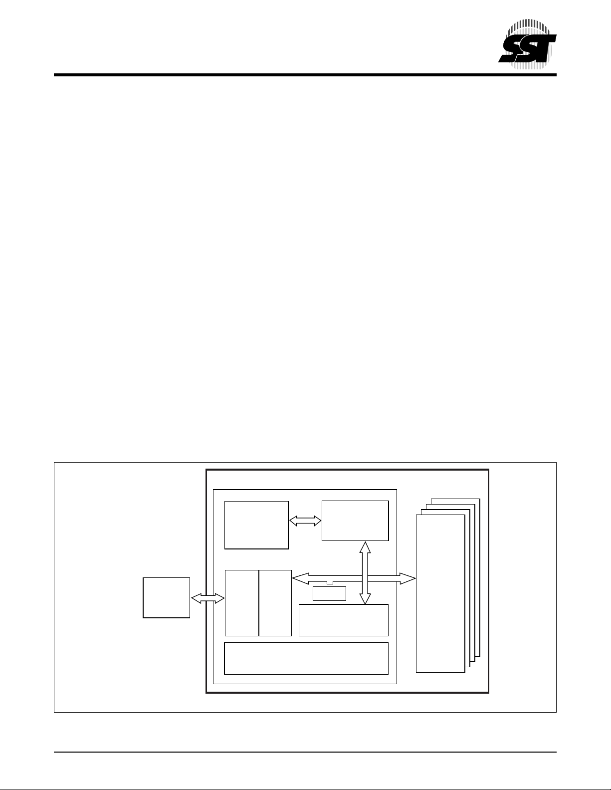
1.0 GENERAL DESCRIPTION
The SST’s CompactFlash card contains a controller,
embedded fir mware storage and flash media in a matchbook sized package with a 50-pin con nector consisti ng of
two rows of 25 female contacts each on 50 mil ( 1.27 m m)
centers. Refer to Figure 1 for SST’s CompactFlash card
block diagram. The controll er interfaces with th e host system allowing data to be wr itten to and rea d from the fla sh
media.
1.1 Performance-optimized ATA Controller
The heart of a CompactFlash card is the ATA controller
which translates standard IDE/ATA signals into flash media
data and controls. SST’s CompactFlash card contains a
proprietary ATA contro ller th at was spec ific ally de sign ed to
attain high data throughput from host to flash. The following
components contribute to the A TA controller’s performance.
1.1.1 Microcontroller Unit (MCU)
The MCU translates IDE/ATA commands into data and
control signals required for flash memory operation.
1.1.2 Internal Direct Memory Access (DMA) Control
The ATA controller inside SST’s CompactFlash card uses
DMA allowing instant data transfer to memory. This implementation eliminates controller overhead associated wit h
traditional, firmware based, memory control, increasing
data transfer rate.
1.1.3 Power Management Unit (PMU)
Power Management Unit control s the power c onsumptio n
of the CompactFlas h ca rd. T h e P MU dram ati cal ly extends
product battery life by putting the part of the circuitry that is
not in operation into sleep mode.
1.1.4 SRAM Buffer
A key contributor to the ATA controller performance is a
SRAM buffer. The buffer optimizes host’s data writes to
flash media.
1.1.5 Embedded Flash File System
Embedded Flash File System is an integral part of the
SST’s ATM contro ller. It contains MCU firmware that performs the f ollow ing tasks:
1. Translates host side signals into flash media
Writes and Reads.
2. Provides flash media wear leveling to spread the
flash writes across all the memory address space
to increase the longevity of flash media.
3. Keeps track of data file structures.
1.1.6 Error Correction Code (ECC)
The ATA Cont r ol l e r c o nt ai n s EC C al g o rithm that c o rr ec t s
3 bytes of error per 512 Byte sector.
ATA Controller
Embedded
Flash
File System
SRAM Buffer
To
Host
PMU
FIGURE 1: SST C
©2001 Silicon Storage Technology, Inc. S71125-03-000 9/01 375
OMPACTFLASH BLOCK DIAGRAM
5
MCU
Flash
Media
ECC
Internal
DMA
375 ILL1-1.4
Page 6
CompactFlash Card
SST48CF008 / 016 / 024 / 032 / 048 / 064 / 096 / 128 / 192 / 256
Data Sheet
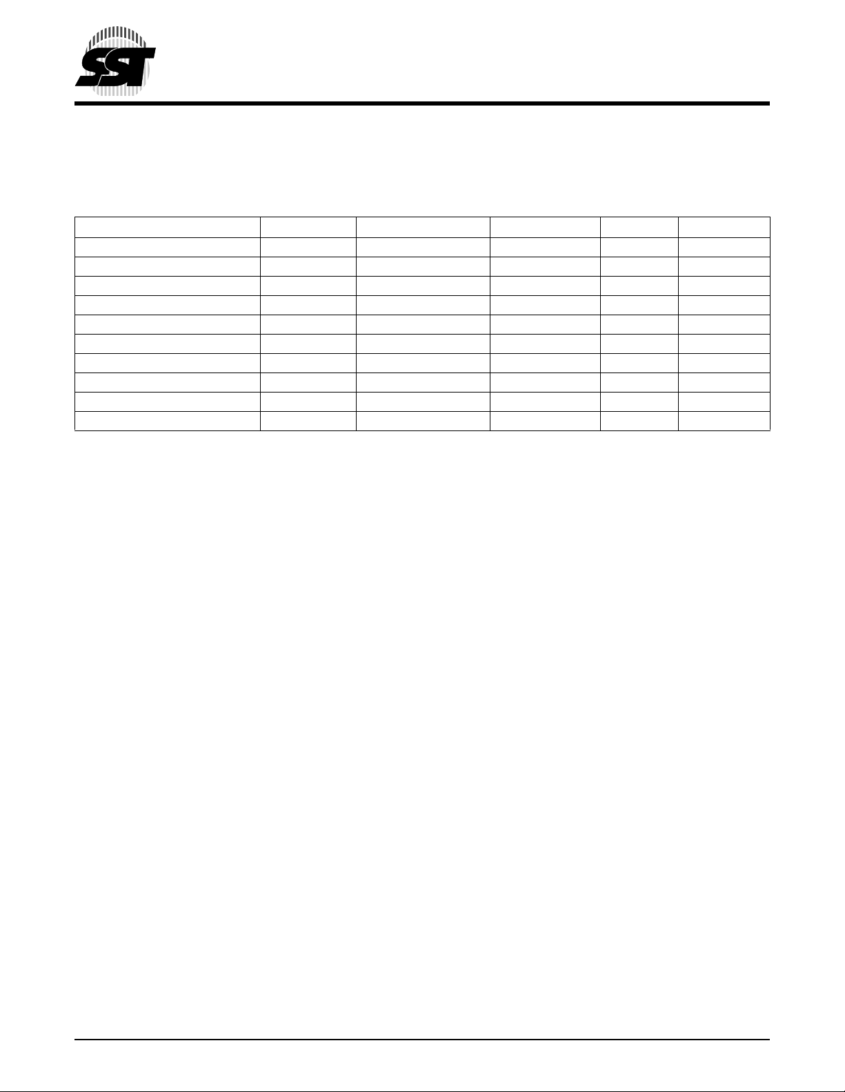
1.2 SST’s CompactFlash Card Product Offering
The SST48CFxxx High Co mpactFlash p roduct family is available in 8 to 256 MBy te densitie s. The following table
shows the specific capacity, default number of cylinder heads, sectors and cylinders for each product line.
.
Model Number Density T ota l Bytes Cylinders Heads Sectors
SST48CF008 8 MB 8,028,160 245 2 32
SST48CF016 16 MB 16,023,552 489 2 32
SST48CF024 24 MB 24,051,712 367 4 32
SST48CF032 32 MB 32,047,104 489 4 32
SST48CF048 48 MB 48,037,888 733 4 32
SST48CF064 64 MB 64,028,672 977 4 32
SST48CF096 96 MB 96,075,776 733 8 32
SST48CF128 128 MB 128,057 ,344 977 8 32
SST48CF192 192 MB 192,151 ,552 733 16 32
SST48CF256 256 MB 256,114 ,688 977 16 32
2.0 ELECTRICAL INTERFACE
2.0.1 Pin Assignment and Pin Type
The signal/pin assignments ar e listed in Table 2-1. Low active signals have a “-” p r ef ix. Pin types are Input, Output or Input/
Output. Section 2.3 defines the DC characteristics for all input and output type structures.
2.1 Electrical De scription
The CompactFlas h car d func tion s in thre e basic mode s: 1) PC Ca rd ATA using I/O Mode, 2) PC Ca rd ATA using Memor y
Mode and 3) True IDE Mode, which is compatible with most disk drives. The configuration of the CompactFlash card will be
controlled using the standard PCMCIA configuration registers starting at address 200H in the Attribute Memory space of the
storage card or for True IDE Mode, pin 9 being grounded.
Table 2-2 desc r i bes the I/O si gna ls. Si gn al s whos e s ourc e i s the hos t ar e desig nat ed as in pu ts whil e sig na ls tha t the Co mpactFlash card sources are outputs. The CompactFlash card logic levels conform to those specified in the PCMCIA Release
2.1 and CFA Specification Rev. 1.4. As shown in Table 2-2, each signal ha s three pos sible operating modes : 1) PC Card
Memory, 2) PC Card I/O and 3) True IDE. All outputs fro m the card ar e tot em po le e x cept th e dat a bu s sign als wh ic h are bi directional tri-state. Refer to Section 2.3 for definitions of Input and Output type.
©2001 Silicon Storage Technology, Inc. S71125-03-000 9/01 375
6
Page 7
CompactFlash Card
SST48CF008 / 016 / 024 / 032 / 048 / 064 / 096 / 128 / 192 / 256
Data Sheet
2.2 Card Pin Assignment
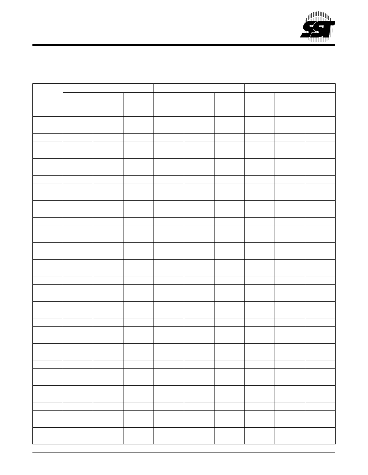
TABLE 2-1: CARD PIN ASSIGNMENT (1 OF 2)
Memory card mode I/O card mode True IDE mode
Signal
1
Name Pin Type I/O Type
Pin No.
Signal
Name Pin Type I/O Type
1 GND - GND GND - GND GND - GND
2D
3D
4D
5D
3
4
5
6
I/O I2D , O2 D
I/O I2D , O2 D
I/O I2D , O2 D
I/O I2D , O2 D
6D7I/O I2D , O2 D
3
4
5
6
7
I/O I2D , O2 D
I/O I2D , O2 D
I/O I2D , O2 D
I/O I2D , O2 D
I/O I2D , O2 D
7-CE1I I3U-CE1I I3U-CS0I I3U
8 A10 I I2D A10 I I2D A10 I I2D
9 -OE I I3U -OE I I3U -ATASEL I I3U
10 A
11 A
12 A
13 V
14 A
15 A
16 A
17 A
18 A
19 A
20 A
21 D
22 D
23 D
9
8
7
DD
6
5
4
3
2
1
0
0
1
2
II2DA9II2DA9II2D
II2DA8II2DA8II2D
II2DA7II2DA7II2D
-- VDD-- VDD-II2DA6II2DA6II2D
II2DA5II2DA5II2D
II2DA4II2DA4II2D
II2DA3II2DA3II2D
II2DA2II2DA2II2D
II2DA1II2DA1II2D
II2DA0II2DA0II2D
I/O I2D , O2 D
I/O I2D , O2 D
I/O I2D , O2 D
0
1
2
I/O I2D , O2 D
I/O I2D , O2 D
I/O I2D , O2 D
24 WP O O2 -IOIS16 O O2 -IOIS16 O O2
25 -CD2 O Ground -CD2 O Ground -CD2 O Ground
26 -CD1 O Ground -CD1 O Ground -CD1 O Ground
27 D
28 D
29 D
30 D
31 D
11
12
13
14
15
I/O I2D , O2 D
I/O I2D , O2 D
I/O I2D , O2 D
I/O I2D , O2 D
I/O I2D , O2 D
11
12
13
14
15
I/O I2D , O2 D
I/O I2D , O2 D
I/O I2D , O2 D
I/O I2D , O2 D
I/O I2D , O2 D
32 -CE2 I I3U -CE2 I I3U -CS1 I I3U
33 -VS1 O Ground -VS1 O Ground -VS1 O Ground
34 -IORD I I3U -IORD I I3U -IORD I I3U
35 -IOWR I I3U -IOWR I I3U -IOWR I I3U
36 -WE I I3U -WE I I3U -WE I I3U
37 RDY/-BSY O O1 -IREQ O O1 INTRQ O O1
38 V
DD
-- VDD-- VDD-39 -CSEL I I2U -CSEL I I2U -CSEL I I2U
40 -VS2 O open -VS2 O open -VS2 O open
Signal
1
Name Pin Type I/O Type
3
4
5
6
7
0
1
2
11
12
13
14
15
I/O I2D, O2
I/O I2D, O2
I/O I2D, O2
I/O I2D, O2
I/O I2D, O2
I/O I2D, O2
I/O I2D, O2
I/O I2D, O2
I/O I2D, O2
I/O I2D, O2
I/O I2D, O2
I/O I2D, O2
I/O I2D, O2
1
©2001 Silicon Storage Technology, Inc. S71125-03-000 9/01 375
7
Page 8
CompactFlash Card
SST48CF008 / 016 / 024 / 032 / 048 / 064 / 096 / 128 / 192 / 256
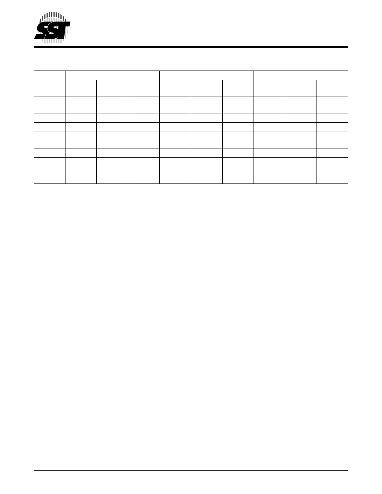
TABLE 2-1: CARD PIN ASSIGNMENT (CONTINUED) (2 OF 2)
Memory card mode I/O card mode True IDE mode
Signal
1
Name Pin Type I/O Type
Pin No.
Signal
Name Pin Type I/O Type
41 RESET I I4U RESET I I4U -RESET I I4U
42 -WAIT O O1 -WAIT O O1 IORDY O O1
43 -INPACK O O1 -INPACK O O1 -INPACK O O1
44 -REG I I3U -REG I I3U -REG I I3U
45 BVD2 O I2U, O1 -SPKR O I2U, O1 -DASP O I2U, O1
46 BVD1 O I2U, O1 -STSCHG O I2U, O1 -PDIAG O I2U, O1
47 D
48 D
49 D
8
9
10
I/O I2D , O2 D
I/O I2D , O2 D
I/O I2D , O2 D
8
9
10
I/O I2D , O2 D
I/O I2D , O2 D
I/O I2D , O2 D
50 GND - GND GND - GND GND - GND
1. Please refer to Sections 2.3.1 to 2.3.4 for detail.
Signal
1
Name Pin Type I/O Type
8
9
10
I/O I2D, O2
I/O I2D, O2
I/O I2D, O2
Data Sheet
1
T2-1.2 375
©2001 Silicon Storage Technology, Inc. S71125-03-000 9/01 375
8
Page 9
CompactFlash Card
SST48CF008 / 016 / 024 / 032 / 048 / 064 / 096 / 128 / 192 / 256
Data Sheet
TABLE 2-2: SIGNAL DESCRIPTION (1 OF 4)
Symbol Type
- A
A
10
0
(PC Card Memory Mode)
- A
A
10
0
(PC Card I/O Mode)
A
- A
2
0
(True IDE Mode
BVD1
(PC Card Memory Mode)
-STSCHG
(PC Card I/O Mode)
Status Changed -PDIAG
(True IDE Mode)
BVD2
(PC Card Memory Mode)
-SPKR
(PC Card I/O Mode)
-DASP
(True IDE Mode)
-CD1, -CD2
(PC Card Memory Mode)
-CD1, -CD2
(PC Card I/O Mode)
-CD1, -CD2
(True IDE Mode)
-CE1, -CE2
(PC Card Memory Mode)
Card Enable
-CE1, -CE2
(PC Card I/O Mode)
Card Enable
-CS0, -CS1
(True IDE Mode)
1
I 8,10,11,12,
Pin Name and Functions
These address lines along with the -REG signa l are used to selec t
14,15,16,17,
18,19,20
the following: The I/O port address registers within the CompactFlash card, the memory mapped port address registers within the
CompactFlash card, a byte in the card’s information s tructure and its
configuration control and status registers.
This signal is the same as the PC Card Memory Mode signal
I 18,19,20 In True IDE Mode only A[2:0] are used to select the one of e ight (True
IDE Mode) registers in the Task File, the remaining address lines
should be grounded by the host.
I/O 46 This s ignal i s asse rted high as the BVD1 sig nal sin ce a bat tery is not
used with this product.
This signal is asserted low to alert the host to changes in the RDY/-
BSY and Write Protect states, while the I/O interface is configured.
Its use is controlled by the Card Config and Status Register.
In the True IDE Mode, this input/output is the Pass Diagnostic signal
in the Master/Slave handshake proto co l.
I/O 45 This output line is always driven to a high state in Memory Mode
since a battery is not required for this product.
This output line is a lways driven to a high state in I /O Mode s ince this
product does not support the audio function.
In the True IDE Mode, this input/output is the Disk Active/Slave
Present signal in the Master/Slave handshake protocol.
O 26,25 These Card Detect pins are connected to ground on the Compact-
Flash card. They are used by the host to determine that the CompactFlash card is fully inserted into its socket.
This signal is the same for all modes.
This signal is the same for all modes.
I 7,32 These input signals are used both to select the card and to indicate
to the card whether a byte or a word operation is being performed. CE2 always accesses the Odd Byte of the word. -CE1 accesses the
Even Byte or the O dd Byte of the wo rd depe nding on A
multiplexing scheme based on A
access all data on D
0-D7
.
, -CE1, -CE2 allows 8 bit hosts to
0
See Tables 2-11, 2-13, 2-16, 2-17, and 2-18.
This signal is the same as the PC Card Memory Mode signal.
In the True IDE Mode CS0 is the chip select f or th e ta sk fil e reg is ters
while CS2 is used to select the Alternate Status Register and the
Device Control Register.
and -CE2. A
0
©2001 Silicon Storage Technology, Inc. S71125-03-000 9/01 375
9
Page 10
SST48CF008 / 016 / 024 / 032 / 048 / 064 / 096 / 128 / 192 / 256
TABLE 2-2: SIGNAL DESCRIPTION (CONTINUED) (2 OF 4)
Symbol Type
-CSEL
(PC Card Memory Mode)
-CSEL
(PC Card I/O Mode)
-CSEL
(True IDE Mode)
D15 - D00
(PC Card Memory Mode)
D15 - D00
(PC Card I/O Mode)
D15 - D00
(True IDE Mode)
GND
(PC Card Memory Mode)
GND
(PC Card I/O Mode)
GND
(True IDE Mode)
-INPACK
(PC Card Memory Mode)
-INPACK
(PC Card I/O Mode)
Input Acknowledge
-INPACK
(True IDE Mode)
-IORD
(PC Card Memory Mode)
-IORD
(PC Card I/O Mode)
-IORD
(True IDE Mode)
-IOWR
(PC Card Memory Mode)
-IOWR
(PC Card I/O Mode)
-IOWR
(True IDE Mode)
1
I 39 This signal is not used for this mode.
I/O 31,30,29,28,
- 1,50 Ground.
O 43 This signal is not used in this mode.
I 34 This signal is not used in this mode.
I 35 This signal is not used in this mode.
Pin Name and Functions
This signal is not used for this mode.
This internally pulled up signal is used to configure this device as a
Master or a Slave when configured in the True IDE Mode. When this
pin is grounded, this device is configured as a Master. When the pin
is open, this device is configured as a Slave.
These lines carry the Data, Commands and Status information
27,49,48,47,
6,5,4,3,2,
23, 22, 21
between the host and th e cont roller. D00 is the LSB of the Even Byte
of the Word. D08 is the LSB of the Odd Byte of the Word.
This signal is the same as the PC Card Memory Mode signal.
In True IDE Mode, all Task File operations occur i n Byte-M ode o n the
low order bus D00-D07 while all data transfers are 16 bit using D00D15.
This signal is the same for all modes.
This signal is the same for all modes.
The Input Acknowledge signal is asserted by the CompactFlash
Card when the card is selected and responding to an I/O read cycle
at the address that is on the address bus. This signal is used by the
host to control the enab le o f any input da ta b uff ers betw een th e CompactFlash card and the CPU.
In True IDE Mode this output signal is not used and should not be
connected at the host.
This is an I/O Read strobe generated by the host. This signal gates
I/O data onto the bus from the CompactFlash Card when the card is
configured to use the I/O interface.
In True IDE Mode, this signal has the same fun cti on as in PC Card
I/O Mode.
The I/O Write strobe pulse is used to clock I/O data on the Card Data
bus into the CompactFlash card controller registers when the CompactFlash card is configured to use the I/O interface.
The clocking will occur on the negative to positive edge of the signal
(trailing edge). In True IDE Mode, this signal has the same function
as in PC Card I/O Mode.
CompactFlash Card
Data Sheet
©2001 Silicon Storage Technology, Inc. S71125-03-000 9/01 375
10
Page 11
CompactFlash Card
SST48CF008 / 016 / 024 / 032 / 048 / 064 / 096 / 128 / 192 / 256
Data Sheet
TABLE 2-2: SIGNAL DESCRIPTION (CONTINUED) (3 OF 4)
Symbol Type
-OE
(PC Card Memory Mode)
-OE
(PC Card I/O Mode)
-ATA SEL
(True IDE Mode)
RDY/-BSY
PC Card Memor y Mode)
-IREQ
PC Card I/O Mode)
INTRQ
(True IDE Mode)
-REG
(PC Card Memory Mode)
-REG
PC Card I/O Mode)
-REG
(True IDE Mode)
RESET
(PC Card Memory Mode)
RESET
(PC Card I/O Mode)
-RESET
(True IDE Mode)
V
DD
(PC Card Memory Mode)
V
DD
(PC Card I/O Mode)
V
DD
(True IDE Mode)
1
Pin Name and Functions
I 9 This is an Output Enable strobe generated by the host interface. It is
used to read data from the Co mpac tFlash card i n Mem ory Mode and
to read the CIS and configuration registers.
In PC Card I/O Mode, this signal is used to read the CIS and configuration registers.
To enable True IDE Mode this input should be grounded by the host.
O 37 In Mem ory Mode this s ignal is s et high w hen the Co mpactFla sh Card
is ready to accept a new data transfer operation and held low when
the card is busy. The Host memory card socket must provide a pullup resistor.
At power up and at Reset, the RDY/-BSY signal is held low (busy)
until the CompactFlash card has completed its power up or reset
function. No access of any type should be made to the CompactFlash card during this time. The RDY/-BSY signal is held high (disabled from being busy) whenever the following condition is true: The
CompactFlash Card has been powered up with +RESET continuously disconnected or asserted.
I/O Operation - A fter the Compac tFlash c ard ha s been confi gured f or
I/O operation, this signal is used as -Interrupt Request. This line is
strobed low to gen erate a pulse mod e i nte rrupt or he ld low fo r a l evel
mode interrupt.
In True IDE Mode signal is the active high Interrupt Request to the
host.
I 44 This signal is used during Memory Cycles to distinguish between
Common Memory and Register (Attribute) M emory Attribute Memory
Select accesses. High for Common Memory, Low for Attribute Memory.
The signal must also be active (low) during I/O Cycles when the I/O
address is on the Bus.
In True IDE Mode this input signal is not used and should be connected to V
by the host.
DD
I 41 When the pin is high, t his signal Resets th e Comp actFlash Card. The
CompactFlash card i s R ese t o nl y at po wer up if this p in is l eft hi gh or
open from power-up . The Compa ctFlash card is also Res et when the
Soft Reset bit in the Card Configuration Option Register is set.
This signal is the same as the PC Card Memory Mode signal.
In the True IDE Mode this input pin is the active low hardware reset
from the host.
- 13,38 +5.0V, +3.3V power.
This signal is the same for all modes.
This signal is the same for all modes.
©2001 Silicon Storage Technology, Inc. S71125-03-000 9/01 375
11
Page 12
SST48CF008 / 016 / 024 / 032 / 048 / 064 / 096 / 128 / 192 / 256
TABLE 2-2: SIGNAL DESCRIPTION (CONTINUED) (4 OF 4)
Symbol Type
-VS1
-VS2
(PC Card Memory Mode)
-VS1
-VS2
(PC Card I/O Mode)
-VS1
-VS2
(True IDE Mode)
-WAIT
(PC Card Memory Mode)
-WAIT
(PC Card I/O Mode)
1
Pin Name and Functions
O3340Voltage Sense Signals. -VS1 is grounded so that the CompactFlash
card CIS can be read at 3.3V and -VS2 i s r ese rved by PCMCIA for a
secondary voltage.
This signal is the same for all modes.
This signal is the same for all modes.
O 42 The -WAIT signal is driven low by the CompactFlash
Card to signal the host to delay completion of a memory or I/O cycle
that is in progress.
This signal is the same as the PC Card Memory Mode signal.
CompactFlash Card
Data Sheet
IORDY
(True IDE Mode)
-WE
(PC Card Memory Mode)
-WE
(PC Card I/O Mode)
-WE
(True IDE Mode)
WP
(PC Card Memory Mode)
Write Protect
-IOIS16
(PC Card I/O Mode)
-IOIS16
(True IDE Mode)
1. I = Input
0 = Output
In True IDE Mode this output signal may be used as IORDY.
I 36 This is a signal driven by the host and used for strobing memory
write data to the registers of the CompactFlash card when the card is
configured in the memory interface mode. It is also used for writing
the configuration registers.
In PC Card I/O Mode, this signal is used for writing the configuration
registers.
In True IDE Mode this input signal is not used and should be connected to V
by the host.
DD
O 24 Memory Mode - The CompactFlash card does not have
a write protect switch. This signal is held low after the completion
of the reset initialization sequence.
I/O Operation - When the CompactFlash card is configured for I/O
Operation Pin 24 is u sed f or the -I/O Selec ted i s 16 Bit Port (-IOIS16)
function. A Low signal indicates that a 16 bit or Odd Byte only operation can be performed at the addressed port.
In True IDE Mode this output signal is asserted low when this device
is expecting a word data transfer cycle.
T2-2.0 375
©2001 Silicon Storage Technology, Inc. S71125-03-000 9/01 375
12
Page 13
CompactFlash Card
SST48CF008 / 016 / 024 / 032 / 048 / 064 / 096 / 128 / 192 / 256
Data Sheet
2.3 Electrical Specification
The following table defines all D.C. Characteristics for the SST CompactFlash card product family.
Unless otherwise stated, conditions are:
Non operating (storage) temperature range -25°C to +85°C
V
= 4.5-5.5V
DD
V
= 3.135-3.465V
DD
Ta = 0°C to +70°C
BSOLUTE MAXIMUM CONDITIONS
A
Parameter Symbol Conditions
Input Powe r V
Voltage on any pin except VDD with respect to GND V -0.5V min. to VDD + 0.5V Max
DD
INPUT POWER
Maximum Average RMS
Voltage
3.135-3.465V 75 mA 200 µA 3.3V at 25°C
4.5-5.5V 100 mA 300 µA 5.0V at 25°C
Active Current
Maximum Average RMS
Sleep Current Measurement Method
-0.3V min. to 6.5V Max
1
1
1. Current measurement is accomplished by connecting an amp meter (set to the 2 amp scale range) in series with the VDD supply to
the CompactFlash card. Current measurements are to be taken while looping on a data transfer command with a sector count of 128.
Current consumption values for both Read and Write commands are not to exceed the Maximum Average RMS Current specified in
this table
CompactFlash produc ts shal l opera te cor rec tl y in bot h voltage ranges as sh own in the table above. To compl y wit h
this specification, current requirements must not exceed the maximum limit.
2.3.1 Input Leakage Current
In the table below, x refers to the characteristics descr ibed in Sectio n 2.3.2. For example, I1U indicates a pul l up
resistor with a type 1 input characteristic.
Type Parameter Symbol Conditions Min Typ Max Units
V
IxZ Input Leakage Current IL
IxU Pull Up Resistor RPU1 VDD = 5.0V 50k 500k Ohm
IxD Pull Down Resistor RPD1 VDD = 5.0V 50k 500k Ohm
= VDD / VIL = GND -1 1 µA
IH
©2001 Silicon Storage Technology, Inc. S71125-03-000 9/01 375
13
Page 14
SST48CF008 / 016 / 024 / 032 / 048 / 064 / 096 / 128 / 192 / 256
2.3.2 Input Characteristics
Type Parameter Symbol
1 Input Voltage
CMOS
2 Input Voltage
CMOS
3 Input Voltage V
CMOS Schmitt Trigger
4 Input Voltage CMOS V
Schmitt Trigger V
2.3.3 Output Drive Type
All output drive type are CMOS level.
2.3.4 Output Drive Characteristics
CompactFlash Card
Data Sheet
Min Typ Max Min Typ Max Units
VDD = 3.3V VDD = 5.0V
V
2.4 2.4 Volts
IH
V
IL
V
2.0 2.7 Volts
IH
V
IL
TH
V
TL
TH
TL
2.0 2.4 Volts
0.5 0.8
1.8 2.4 Volts
0.9 0.8
0.6 0.8
0.8 0.8
Type Parameter Symbol Conditions Min Typ Max Units
O1 Output Voltage VOH I
V
OL
O2 Output Voltage V
I
OH
V
OL
= -4 mA V
OH
-0.8V Volts
DD
IOL = 4 mA GND +0.4V
= -8 mA V
OH
-0.8V Volts
DD
IOL = 8 mA GND +0.4V
2.3.5 Interface/Bus Timing
There are two types of bus cycles and timing sequences that occur in the PCMCIA type interface, a direct mapped
I/O transfer and a memory access. The two timing sequences are explained in detail in the PCMCIA PC Card Standard. SST’s CompactFlash card conforms to the timing in that reference document.
©2001 Silicon Storage Technology, Inc. S71125-03-000 9/01 375
14
Page 15
CompactFlash Card
SST48CF008 / 016 / 024 / 032 / 048 / 064 / 096 / 128 / 192 / 256
Data Sheet
2.3.6 Attribute Memory Read Timing Specification
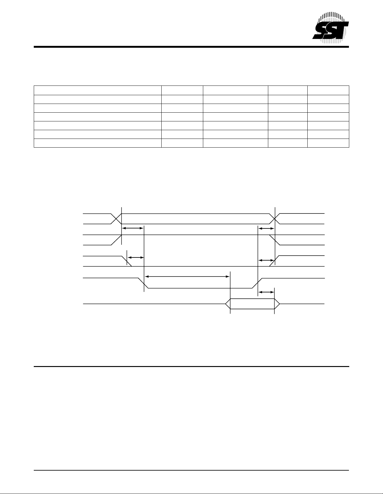
The Attribute Memory access time is defined as 100 ns. Detailed timing specifications are shown in Table 2-3.
TABLE 2-3: ATTRIBUTE MEMORY READ TIMING
Speed Version 100 ns
Item Symbol IEEE Symbol Min
Read Cycle Time tc(R) tAVAV 100
Address Access Time ta(A) tAVQV 100
Card Enable Access Time ta(CE) tELQV 100
Output Enable Access Time ta(OE) tGLQV 50
Output Disable Time from CE tdis(CE) tEHQZ 50
Output Disable Time from OE tdis(OE) tGHQZ 50
Address Setup Time tsu(A) tAVGL 10
Output Enable Time from CE ten(CE) tELQNZ 5
Output Enable Time from OE ten(OE) tGLQNZ 5
Data Valid from Address Change tv(A) tAXQX 0
1. All times are in nanoseconds. D
signal and the -WE signal must be de-asserted between consecutive cycle operations.
All AC specifications are guaranteed by design.
signifies data provided by the CompactFlash card to the system. The -CE signal or both the -OE
OUT
1
Max
T2-3.1 375
1
tc(R)
An
-REG
tsu(A)
ta(A)
ta(CE)
-CE
ten(CE)
ta(OE)
-OE
ten(OE)
Dout
FIGURE 2-1: ATTRIBUTE MEMORY READ TIM I N G DIAGRAM
tv(A)
tdis(CE)
tdis(OE)
Dout
375 ILL2-1.0
©2001 Silicon Storage Technology, Inc. S71125-03-000 9/01 375
15
Page 16
CompactFlash Card
SST48CF008 / 016 / 024 / 032 / 048 / 064 / 096 / 128 / 192 / 256
Data Sheet
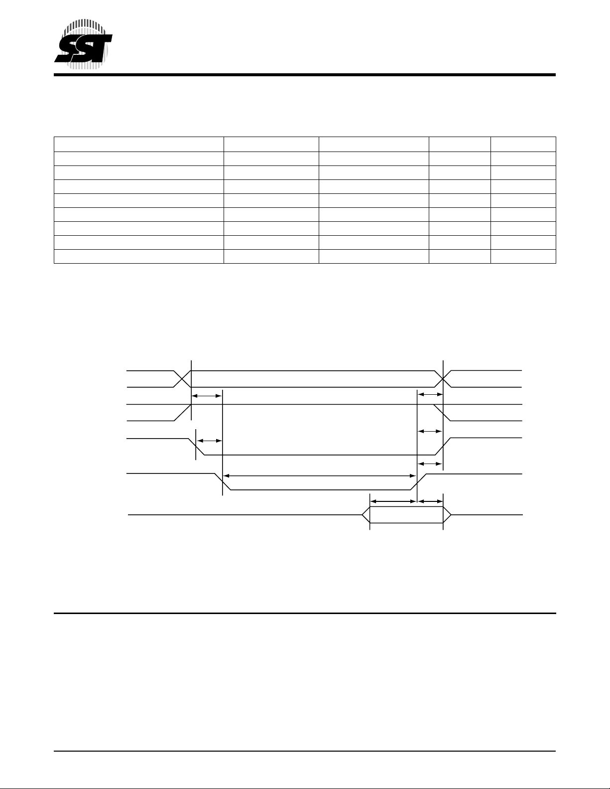
2.3.7 Configuration Register (Attribute Memory) Write Timing specification
The Card Configuration write access time is defined as 100 ns. Detailed timing specifications are shown in Table 2-4.
TABLE 2-4: CONFIGURATION REGISTER (ATTRIBUTE MEMORY) WRITE TIMING
Speed Version 100 ns
Item Symbol IEEE Symbol Min
Write Cycle Time tc(W) tAVAV 100
Write Pulse Width tw(WE) tWLWH 60
Address Setup Time tsu(A) tAVWL 10
Write Recovery Time trec(WE) tWMAX 15
Data Setup Time for WE tsu(D-WEH) tDVWH 40
Data Hold Time th(D) tWMDX 15
1. All times are in nanoseconds. DIN signifies data provided by the system to the CompactFlash card.
All AC specifications are guaranteed by design.
1
Max
T2-4.1 375
1
tc(W)
-Reg
An
tsu(A)
tw(WE)
trec(WE)
-WE
tsu(D-WEH)
-CE
-OE
Din
FIGURE 2-2: CONFIGURATION REGISTER (ATTRIBUTE MEMORY) WRITE TIMING DIAGRAM
Din Valid
375 ILL2-2.0
th(D)
©2001 Silicon Storage Technology, Inc. S71125-03-000 9/01 375
16
Page 17
CompactFlash Card
SST48CF008 / 016 / 024 / 032 / 048 / 064 / 096 / 128 / 192 / 256
Data Sheet
2.3.8 Common Memory Read Timing Specification
TABLE 2-5: COMMON MEMORY READ TIMING
Item Symbol IEEE Symbol Min1 ns
Output Enable Access Time ta(OE) tGLQV 50
Output Disable Time from OE tdis(OE) tGHQZ 50
Address Setup Time tsu(A) tAVGL 10
Address Hold Time th(A) tGHAX 15
CE Setup before OE ts u(CE ) tELGL 0
CE Hold following OE th(CE) tGHEH 15
1. All times are in nanoseconds.
All AC specifications are guaranteed by design.
Max1 ns
T2-5.1 375
An
tsu(A)
-REG
-CE
tsu(CE)
ta(OE)
-OE
Dout
FIGURE 2-3: CO MMON MEM ORY READ TIMING DIAGRAM
th(A)
th(CE)
tdis(OE)
Dout
375 ILL2-3.0
©2001 Silicon Storage Technology, Inc. S71125-03-000 9/01 375
17
Page 18
CompactFlash Card
SST48CF008 / 016 / 024 / 032 / 048 / 064 / 096 / 128 / 192 / 256
2.3.9 Common Memory Write Timing Specification
TABLE 2-6: COMMON MEMORY WRITE TIMING
Item Symbol IEEE Symbol Min1 ns
Data Setup before WE tsu(D-WEH) tDVWH 40
Data Hold following WE th(D) tWMDX 15
WE Pulse Width tw(WE) tWLWH 60
Address Setup Time tsu(A) tAVWL 10
CE Setup before WE tsu(CE) tELWL 0
Write Recovery Time trec(WE) tWMAX 15
Address Hold Time th(A) tGHAX 15
CE Hold following WE th(CE) tGHEH 15
1. All times are in nanoseconds.
All AC specifications are guaranteed by design.
Data Sheet
Max1 ns
T2-6.1 375
An
tsu(A)
-REG
-CE
tsu(CE)
tw(WE)
-WE
Din
tsu(D-WEH)
FIGURE 2-4: CO MMON MEM ORY WRITE TIMING DIAGRAM
th(A)
th(CE)
trec(WE)
th(D)
Din Valid
375 ILL2-4.0
©2001 Silicon Storage Technology, Inc. S71125-03-000 9/01 375
18
Page 19

CompactFlash Card
SST48CF008 / 016 / 024 / 032 / 048 / 064 / 096 / 128 / 192 / 256
Data Sheet
2.3.10 I/O Input (Read) Timing Specification
TABLE 2-7: I/O READ TIMING
Item Symbol IEEE Symbol Min
Data Delay after IORD td(IORD) tlGLQV 100
Data Hold following IORD th(IORD) tlGHQX 0
IORD Width Time tw(IORD) tlGLIGH 165
Address Setup before IORD tsuA(IORD) tAVIGL 70
Address Hold following IORD thA(IORD) tlGHAX 20
CE Setup before IORD tsuCE(IORD) tELIGL 5
CE Hold following IORD thCE(IORD) tlGHEH 20
REG Setup before IORD tsuREG(IORD) tRGLIGL 5
REG Hold following IORD thREG(IORD) tlGHRGH 0
INPACK Delay Falling from IORD tdfINPACK(IORD) tlGLIAL 0 45
INPACK Delay Rising from IORD tdrINPACK(IORD) tlGHIAH 45
IOIS16 Delay Falling from Address tdfIOIS16(ADR) tAVISL 35
IOIS16 Delay Rising from Address tdrIOIS16(ADR) tAVISH 35
1. All times are in nanoseconds.
Note: The maximum load on -INPACK and -IOIS16 is 1 LSTTL with 50pF total load.
All AC specifications are guaranteed by design.
1
Max
1
T2-7.1 375
An
tsuA(IORD)
-REG
-CE
tsuREG(IORD)
tsuCE(IORD)
-IORD
-INPACK
-IOIS16
tdfIOIS16(ADR)
Dout
FIGURE 2-5: I/O READ TIMING DIAGRAM
thA(IORD)
thREG(IORD)
thCE(IORD)
tw(IORD)
tdrINPACK(IORD)
tdfINPACK(IORD)
tdrIOIS16(ADR)
td(IORD)
th(IORD)
Dout
375 ILL2-5.0
©2001 Silicon Storage Technology, Inc. S71125-03-000 9/01 375
19
Page 20

CompactFlash Card
SST48CF008 / 016 / 024 / 032 / 048 / 064 / 096 / 128 / 192 / 256
Data Sheet
2.3.11 I/O Output (Write) Timing Specification
TABLE 2-8: I/O WRITE TIMING
Item Symbol IEEE Symbol Min
Data Setup before IOWR tsu(IOWR) tDVIWH 60
Data Hold following IOWR th(IOWR) tlWHDX 30
IOWR Width Time tw(IOWR) tlWLIWH 165
Address Setup before IOWR tsuA(IOWR) tAVIWL 70
Address Hold following IOWR thA(IOWR) tlWHAX 20
CE Setup before IO WR tsuCE(IOWR) tELIWL 5
CE Hold following IOWR thCE(IOWR) tlWHEH 20
REG Setup before IOWR tsuREG(IOWR) tRGLIWL 5
REG Hold following IOWR thREG(IOWR) tlWHRGH 0
IOIS16 Delay Falling from Address tdfIOIS16(ADR) tAVISL 35
IOIS16 Delay Rising from Address tdrIOIS16(ADR) tAVISH 35
1. All times are in nanoseconds.
Note: The maximum load on -INPACK, and -IOIS16 is 1 LSTTL with 50pF total load.
All AC specifications are guaranteed by design.
1
Max
T2-8.1 375
1
An
tsuA(IOWR)
-REG
tsuREG(IOWR)
tsuCE(IOWR)
-CE
-IOWR
-IOIS16
tdfIOIS16(ADR)
Din
FIGURE 2-6: I/O WRITE TIMING DIAGRAM
thA(IOWR)
thREG(IOWR)
thCE(IOWR)
tw(IOWR)
tdrIOIS16(ADR)
tsu(IOWR)
th(IOWR)
Din Valid
375 ILL2-6.0
©2001 Silicon Storage Technology, Inc. S71125-03-000 9/01 375
20
Page 21

CompactFlash Card
SST48CF008 / 016 / 024 / 032 / 048 / 064 / 096 / 128 / 192 / 256
Data Sheet
2.3.12 True IDE Mode I/O Input (Read) Timing Specification
TABLE 2-9: TRUE IDE MODE I/O REA D TIM I NG DIAGRAM
Item Symbol IEEE Symbol Min1
Data Delay after IORD td(IORD) tlGLQV 50
Data Hold following IORD th(IORD) tlGHQX 5
IORD Width Time tw(IORD) tlGLIGH 70
Address Setup before IORD tsuA(IORD) tAVIGL 25
Address Hold following IORD thA(IORD) tlGHAX 10
CE Setup before IORD tsu CE(IO RD ) tELIGL 10
CE Hold following IORD thCE(IORD) tlGHEH 5
IOIS16 Delay Falling from Address tdfIOIS16(ADR) tAVISL 20
IOIS16 Delay Rising from Address tdrIOIS16(ADR) tAVISH 20
1. All times are in nanoseconds.
Note: The maximum load on -IOIS16 is 1 LSTTL with 50pF total load.
All AC specifications are guaranteed by design.
1
Max
T2-9.2 375
An
tsuA(IORD)
-CE
tsuCE(IORD)
tw(IORD)
-IORD
-IOIS16
td(IORD)
tdfIOIS16(ADR)
Dout
FIGURE 2-7: TRUE IDE MODE I/O READ TIMING DIAGRAM
thA(IORD)
thCE(IORD)
tdrIOIS16(ADR)
th(IORD)
Dout
375 ILL2-7.0
©2001 Silicon Storage Technology, Inc. S71125-03-000 9/01 375
21
Page 22

SST48CF008 / 016 / 024 / 032 / 048 / 064 / 096 / 128 / 192 / 256
2.3.13 True IDE Mode I/O Output (Write) Timing Specification
CompactFlash Card
Data Sheet
TABLE 2-10: T
Item Symbol IEEE Symbol Min
Data Setup before IOWR tsu(IOWR) tDVIWH 20
Data Hold following IOWR th(IOWR) tlWHDX 10
IOWR Width Time tw(IOWR) tlWLIWH 70
Address Setup before IOWR tsuA(IOWR) tAVIWL 25
Address Hold following IOWR thA(IOWR) tlWHAX 10
CE Setup before IO WR tsuCE(IOWR) tELIWL 10
CE Hold following IOWR thCE(IOWR) tlWHEH 5
IOIS16 Delay Falling from Address tdfIOIS16(ADR) tAVISL 20
IOIS16 Delay Rising from Address tdrIOIS16(ADR) tAVISH 20
1. All times are in nanoseconds.
Note: The maximum load on -IOIS16 is 1 LSTTL with 50pF total load.
All AC specifications are guaranteed by design.
RUE IDE MODE I/O WRITE TIMING
1
Max
An
-CE
tsuA(IOWR)
tsuCE(IOWR)
tw(IOWR)
thA(IOWR)
thCE(IOWR)
1
T2-10.2 375
-IORD
tdrIOIS16(ADR)
-IOIS16
tdfIOIS16(ADR)
Din
Din Valid
FIGURE 2-8: True IDE Mode I/O Write Timing Diagram
©2001 Silicon Storage Technology, Inc. S71125-03-000 9/01 375
22
th(IOWR)tsu(IOWR)
375 ILL2-8.0
Page 23

CompactFlash Card
SST48CF008 / 016 / 024 / 032 / 048 / 064 / 096 / 128 / 192 / 256
Data Sheet
2.4 Card Configuration
The CompactFlash cards are identi fi ed by approp r iat e infor ma tio n in the Car d Information Structure (CIS) . The following configuration registers are used to coordinate the I/O spaces and the Interrupt level of cards that are located
in the system. In addition , these registers pr ovide a method for accessing status information about the Com pactFlash card that may be used to arbitrate between multiple interrupt sources on the same interrupt level or to
replace status information that appears on dedicated pins in memory cards that have alternate use in I/O cards.
TABLE 2-11: REGISTERS AND MEM OR Y S PACE DECOD IN G
-CE2 -CE1 -REG -OE -WE A10A9A8-A4A3A2A1A0Selected Space
1 1 X X XXXXXXXXXStandby
X 0 0 0 1 0 1 XX X X X 0 Configuration Registers Read
1 0 1 0 1 X X XX X X X X Common Memory Read (8 bit D
0 1 1 0 1 X X XX X X X X Common Memory Read (8 bit D15-D8)
0 0 1 0 1 X X XX X X X 0 Common Memory Read (16 bit D15-D0)
X 0 0 1 0 0 1 XX X X X 0 Configuration Registers Write
1 0 1 1 0 X X XX X X X X Common Mem ory Write (8 bit D
0 1 1 1 0 X X XX X X X X Common Mem ory Write (8 bit D15-D8)
0 0 1 1 0 X X XX X X X 0 Common Memory Write (16 bit D15-D0)
X 0 0 0 1 0 0 XX X X X 0 Card Information Structure Read
1 0 0 1 0 0 0 XX X X X 0 Invalid Access (CIS Writ e)
1 0 0 0 1 X X XX X X X 1 Invalid Access (Odd Att ribute Read)
1 0 0 1 0 X X XX X X X 1 Invalid Access (Odd Attribute Write)
0 1 0 0 1 X X XX X X X X Invalid Access (Odd Attribute Read)
0 1 0 1 0 X X XX X X X X Invalid Access (Odd Attribute Write)
)
7-D0
)
7-D0
T2-11.0 375
TABLE 2-12: CONFIGURATION REGISTERS DECODING
-CE2 -CE1 -REG -OE -WE A10A9A8-A4A3A2A1A0Selected Register
X 0 0 0 1 0 1 00 0 0 0 0 Configuration Option Reg Read
X 0 0 1 0 0 1 00 0 0 0 0 Configuration Option Reg Write
X 0 0 0 1 0 1 00 0 0 1 0 Card Status Register Read
X 0 0 1 0 0 1 00 0 0 1 0 Card Status Register Write
X 0 0 0 1 0 1 00 0 1 0 0 Pin Replacement Register Read
X 0 0 1 0 0 1 00 0 1 0 0 Pin Replacement Register Write
X 0 0 0 1 0 1 00 0 1 1 0 Socket and Copy Register Read
X 0 0 1 0 0 1 0 0 0 1 1 0 Socket and Copy Register Write
Note: The location of the card configuration registers should always be read from the CIS locations 0000H to 0198H. No writes should be per-
formed to the CompactFlash card attribute memory except to the card configuration register addresses. All other attribute memory locations are reserved.
T2-12.0 375
©2001 Silicon Storage Technology, Inc. S71125-03-000 9/01 375
23
Page 24

CompactFlash Card
SST48CF008 / 016 / 024 / 032 / 048 / 064 / 096 / 128 / 192 / 256
Data Sheet
2.4.1 Attribute Memory Function
Attribute memor y is a spa ce wher e Comp ac tF lash c ar d ide ntif icati on an d con fig urati on in form ation ar e st or ed, an d
is limited to 8-bit wide accesses only at even addresses. The card configuration registers are also located here.
For the Attribute Memor y Read function, s ignals -REG and -O E must be active and -WE i nacti ve during t he cycl e.
As in the Main Memor y Read fun ctions, the si gnals -CE1 an d -CE2 cont rol the Even Byte and O dd Byte addre ss,
but only the Even Byte data is valid during the Attribute Memory access. Refer to Tab le 2-13 below for signal states
and bus validity for the Attribute Memory function.
TABLE 2-13: A
Function Mode -REG -CE2 -CE1 A10A9A0-OE -WE D15-D
Standby Mode X V
Read Byte Access CIS ROM (8 bits) V
Write Byte Access CIS (8 bits) (Invalid) V
Read Byte Access Configuration (8 bits) V
Write Byte Access Configuration (8 bits) V
Read Word Access CIS (16 bits) V
Write Word Access CIS (16 bits) (Invalid) V
Read Word Access Configuration (16 bits) V
Write Word Access Configuration (16 bits) V
Note: The -CE signal or both the -OE signal and the -WE signal must be de-asserted between consecutive cycle operations.
TTRIBUTE MEMORY FUNCTION
8
V
IH
V
IL
V
IL
V
IL
V
IL
V
IL
V
IL
V
IL
V
IL
V
IH
V
IH
V
IH
V
IH
V
IL
V
IL
V
IL
V
IL
X X X X X High Z High Z
IH
VILVILVILVILV
IL
VILVILVILV
IL
VILVIHVILVILV
IL
VILVIHVILV
IL
VILVILXVILV
IL
VILVILXVIHVILDon’t Care Even Byte
IL
VILVIHXVILV
IL
VILVIHXVIHVILDon’t Care Even Byte
IL
IHVIL
IHVIL
High Z Even Byte
IH
Don’t Care Even Byte
High Z Even Byte
IH
Don’t Care Even Byte
Not Valid Even Byte
IH
Not Valid Even Byte
IH
D7-D
0
T2-13.0 375
2.4.2 Configuration Option Register (Address 200H in Attribute Memory)
The Configuration Option Regist er is used to confi gure the cards interface, address decodin g and interr upt and to
issue a soft reset to the CompactFlash card.
OperationD7D6D5D4D3D2D1D0
R/W SRESET LevlREQ Conf5 Conf4 Conf3 Conf2 Conf1 Conf0
SRESET Soft Reset - Setting this bit to one (1), waiting the minimum reset width time and
returning to zero (0) places th e Compa ctFlash c ard in the Reset s tate. Settin g this bit to
one (1) is equi valent to asser tion of the +RESE T signal except that th e SRESET bit is
not cleared. Retur n in g thi s b it to zero (0) l eaves the CompactF la sh ca rd in th e s ame unconfigured Reset sta te as following power-up and ha rdware reset. T his bit is set to zer o
(0) by power-up and hardware reset. Using the PCMCIA Soft Reset is considered a hard
Reset by the ATA Commands. Contrast with Soft Reset in the Device Control Register.
LevlREQ This bit is set to one (1) when Level Mode Interrupt is selected, and zero (0) when Pulse
Mode is selected. Set to zero (0) by Reset.
Conf5 Conf0 Configuratio n Index. Set to zero (0) by reset. It’s used to select operation mode of
the CompactFlash card as shown below.
Note: Conf5 and Conf4 are reserved and must be written as (0).
©2001 Silicon Storage Technology, Inc. S71125-03-000 9/01 375
24
Page 25

CompactFlash Card
SST48CF008 / 016 / 024 / 032 / 048 / 064 / 096 / 128 / 192 / 256
Data Sheet
TABLE 2-14: C
Conf5 Conf4 Conf3 Conf2 Conf1 Conf0 Disk Card Mode
000000Memory Mapped
000001I/O Mapped, any 16 Byte system
000010I/O Mapped, 1F0H-1F7H/3F6H-3F7H
000011I/O Mapped, 170H-177H/376H-377H
ARD CONFIGURATIONS
decoded boundary
T2-14.0 375
2.4.3 Card Configuration and Status Register (Address 202H in Attribute Memory)
The Card Configuration and Status Register contains information about the card’s condition.
CARD CONFIGURATION AND STATUS REGISTER O RGANIZATION
OperationD7D6D5D4D3D2D1D0
Read Changed SigChg IOis8 0 0 PwrDwn Int 0
Write 0 SigChg IOis8 0 0 PwrDwn 0 0
Changed Indicates that one or both of the Pin Replacement r egister CRdy or CWProt bits are se t
to one (1). When the Chan ged bit i s se t, Pin 4 6 (-STSCH G) is h eld low if th e SigCh g bit
is a One (1) and the CompactFlash card is configured for the I/O interface.
SigChg This b it is set and res et by the host to en able and disable a state-ch ange “signal” f rom
the Status Register, the Changed bit control pin 46 the Changed Status signal. If no state
change signal is d esired , this bit shou ld be s et to zer o (0) a nd pin 46 ( -STSCH G) si gnal
will be held high while the CompactFlash card is configured for I/O
IOis8 The host sets this bit to a one (1) if the CompactFlash card is to be configured in an 8-bit
I/O Mode. The CompactFlash card is always configured for both 8- and 16-bit I/O, so this
bit is ignored.
PwrDwn This bit indicates whether the host requests the CompactFlash card to be in the power
saving or active mode. When the bit is one ( 1), the CompactFla sh card enters a p ower
down mode. When zero (0), the host is reques ting the Compac tFlash card to enter the
active mode. The PCMCIA Rdy/-Bsy value becomes BUSY when t his bit is changed.
Rdy/-Bsy will not become Re ady unti l the power state requ ested has been en tered . The
CompactFlash card automatically powers down when it is idle and powers back up when
it receives a command.
Int This bit represents the internal state of the interrupt request. This value is available
whether or not I/O interface has been configured. This signal remains true until the
condition which caused the interrupt request has been serviced. If interrupts are
disabled by the -IEN bit in the Device Control Register, this bit is a zero (0).
©2001 Silicon Storage Technology, Inc. S71125-03-000 9/01 375
25
Page 26

CompactFlash Card
SST48CF008 / 016 / 024 / 032 / 048 / 064 / 096 / 128 / 192 / 256
Data Sheet
2.4.4 Pin Replacement Register (Address 204H in Attribute Memory)
OperationD7D6D5D4D3D2D1D0
Read 0 0 CRdy/-Bsy CWProt 1 1 Rdy/-Bsy 0
Write 0 0 CRdy/-Bsy CWProt 0 0 MRdy/-Bsy X
CRdy/-Bsy This bit is set to one (1) when the bit RRdy/-Bsy change s state. This bit can also be
written by the host.
CWProt This bit is set to one (1) when the RWprot changes state. This bit may also be written by
the host.
Rdy/-Bsy This bit is used to deter mine the inter nal state of the Rdy/ -Bsy signal. This bit m ay be
used to determi ne the s tate of the Ready/ -Busy as this pin ha s been realloc ated for use
as Interrupt Request on an I/O car d. When written, this bit acts as a ma sk for writi ng th e
corresponding bit CRdy/-Bsy.
MRdy/-Bsy This bit acts as a mask for writing the corresponding bit CRdy/-Bsy.
X This bit is ignored by the CompactFlash card.
TABLE 2-15: PIN REPLACEMENT CHANGED BIT/MASK BIT VALUES
Written by Host
Initial Value of (C) Status
0 X 0 0 Unchanged
1 X 0 1 Unchanged
X 0 1 0 Cleared by Host
X 1 1 1 Set by Host
Final “C” Bit Comments“C” Bit “M” Bit
T2-15.0 375
2.4.5 Socket and Copy Register (Address 206H in Attribute Memory)
This register contains additional configuration information. This register is always written by the system before writing the card’s Configuration Index Register.
SOCKET AND COPY REGISTER ORGANIZATION:
OperationD7D6D5D4D3D2D1D0
Read 0 0 CRdy/-Bsy CWProt 1 1 Rdy/-Bsy 0
Write 0 0 CRdy/-Bsy CWProt 0 0 MRdy/-Bsy X
Reserved This bit is reserved for future standardization. This bit must be set to zero (0) by the
software when the register is written.
Drive # This bit indicates the drive number of the card for twin card configuration. Twin card
configuration is currently not supported.
X The socket number is ignored by the CompactFlash card.
©2001 Silicon Storage Technology, Inc. S71125-03-000 9/01 375
26
Page 27

CompactFlash Card
SST48CF008 / 016 / 024 / 032 / 048 / 064 / 096 / 128 / 192 / 256
Data Sheet
2.5 I/O Transfer Function
2.5.1 I/O Function
The I/O transfer to or from the Comp actFlash card can be eithe r 8 or 16 bits. When a 16-bit access ible port is
addressed, the signal -IOIS16 is asserted by the CompactFlash card. Otherwise, the -IOIS16 signal is de-asserted.
When a 16 bit transfer is at temp ted, an d th e - IO IS 16 si gna l i s not as se rted by the Comp actF las h ca rd, the system
must generate a pair of 8-b it references to access the word’s Even Byte and Odd Byte. Th e CompactFlash card
permits both 8 and 16 bit accesses to all of its I/O addresses, so -IOIS16 is asserted for all addresses to which the
CompactFlash card responds.
TABLE 2-16: I/O F
UNCTION
Function Code -REG -CE2 -CE1 A0 -IORD -IOWR D15-D
Standby Mode X V
Byte Input Access
(8 bits)
Byte Output Access
(8 bits)
Word Input Access
V
IL
V
IL
V
IL
V
IL
V
IL
IH
V
IH
V
IH
V
IH
V
IH
V
VIL VIL VIL VIH Odd Byte Even Byte
IL
V
IH
V
IL
V
IL
V
IL
V
IL
XXXHigh Z High Z
V
IL
V
IH
V
IL
V
IH
V
IL
V
IL
V
IH
V
IH
V
IH
V
IH
V
IL
V
IL
High Z
High Z
Don’t Care
Don’t Care
(16 bits)
Word Output Access
V
VIL VIL VIL VIH VIL Odd Byte Even Byte
IL
(16 bits)
I/O Read Inhibit
I/O Write Inhibit
High Byte Input Only
V
X X X VIL V
IH
V
X X X VIH VIL High Z High Z
IH
V
VIL VIH X VIL V
IL
IH
IH
Don’t Care Don’t Care
Odd Byte High Z
(8 bits)
High Byte Output
V
VIL VIH X VIH V
IL
IL
Odd Byte Don’t Care
Only (8 bits)
8
D7-D
0
Even Byte
Odd Byte
Even Byte
Odd Byte
T2-16.0 375
©2001 Silicon Storage Technology, Inc. S71125-03-000 9/01 375
27
Page 28

CompactFlash Card
SST48CF008 / 016 / 024 / 032 / 048 / 064 / 096 / 128 / 192 / 256
2.6 Common Memory Transfer Function
2.6.1 Common Memory Function
The Common Memory Transfer to or from the CompactFlash card can be either 8 or 16 bits.
The CompactFlash card permits both 8 and 16 bit accesses to all of its Common Memory addresses.
Data Sheet
TABLE 2-17: C
OMMON MEMORY F UNCTION
Function Code -REG -CE2 -CE1 A0 -OE -WE D15-D
Standby Mode X V
Byte Read Access
(8 bits)
Byte-Write Access
(8 bits)
Word Read Access
V
IH
V
IH
V
IH
V
IH
V
IH
IH
V
IH
V
IH
V
IH
V
IH
V
IL
V
IH
V
IL
V
IL
V
IL
V
IL
V
IL
X X X High Z High Z
V
V
V
V
X V
V
IL
IH
IL
IH
IL
V
IL
V
IH
V
IH
IL
V
IH
V
IH
V
IL
V
IL
V
IH
High Z
High Z
Don’t Care
Don’t Care
Odd Byte Even Byte
(16 bits)
Word-Write Access
V
IH
V
IL
V
IL
X V
IH
V
IL
Odd Byte Even Byte
(16 bits)
Odd Byte Read Only
V
IH
V
IL
V
IH
X V
IL
V
IH
Odd Byte High Z
(8 bits)
Odd Byte-Write Only
V
IH
V
IL
V
IH
X V
IH
V
IL
Odd Byte D on’t Care
(8 bits)
8
D7-D
0
Even Byte
Odd Byte
Even Byte
Odd Byte
T2-17.0 375
©2001 Silicon Storage Technology, Inc. S71125-03-000 9/01 375
28
Page 29

CompactFlash Card
SST48CF008 / 016 / 024 / 032 / 048 / 064 / 096 / 128 / 192 / 256
Data Sheet
2.7 True IDE Mode I/O Transfer Function
2.7.1 True IDE Mode I/O Function
The CompactFlash card can be configured in a True IDE Mode of operation. The CompactFlash card is configured
in this mode only whe n the -OE inp ut sign al i s grounded by the host during th e power off to p ower on cycl e. In this
Tr ue IDE Mode th e PCMCIA pr otocol and con figuration are d isabled and only I/ O operations to the Task File and
Data Register are a llowed. In this mode no Memor y or Attribute Re gisters are accessible to the host. CompactFlash cards permit 8 bit data accesses if the user issues a Set Feature Command to put the device in 8 bit Mode.
Note: Removing and reinserting the CompactFlash card while the host computer’s power is on will reconfigure the
CompactFlash to PC Card ATA mode from the origin al True IDE Mode. To configur e the Compa ct Flas h c ard
in Tr ue IDE Mode, the 50-pin socket must be power cycled with the Comp actFlash card in serted and -OE
(output enable) asserted.
Table 2-18 defines the function of the operations for the True IDE Mode.
TABLE 2-18: T
RUE IDE MODE I/O FUNCTION
Function Code -CE2 -CE1 A0-A2 -IORD -IOWR D15-D
Invalid Mode V
Standby Mode V
Task File Wri te
Task File Read V
Data Register Write
Data Register Read
Control Register Write V
Alt Status Read
Drive Address
IL
IH
V
IH
IH
V
IH
V
IH
IL
V
IL
V
IL
V
IL
V
IH
V
IL
V
IL
V
IL
V
IL
V
IH
V
IH
V
IH
X X X High Z High Z
X X X High Z High Z
1-7H V
1-7H V
0 V
0 V
6H V
6H V
7H V
IH
IL
IH
IL
IH
IL
IL
V
IL
V
IH
V
IL
V
IH
V
IL
V
IH
V
IH
Don’t Care Data In
High Z Data Out
Odd Byte In Even Byte In
Odd Byte Out Even Byte Out
Don’t Care Control In
High Z Status Out
High Z Data Out
8
D7-D
0
T2-18.0 375
©2001 Silicon Storage Technology, Inc. S71125-03-000 9/01 375
29
Page 30

CompactFlash Card
SST48CF008 / 016 / 024 / 032 / 048 / 064 / 096 / 128 / 192 / 256
Data Sheet
3.0 SOFTWARE INTERFACE
3.1 CF-ATA Drive Register Set Definition and Protocol
The CompactFlash card can be configured as a high performance I/O device through:
1. Standard PC-AT disk I/O address spaces 1F0H-1F7H, 3F6H-3F7H (primary);
170H-177H, 376H-377H (secondary) with IRQ 14 (or other available IRQ).
2. Any system decoded 16 Byte I/O block using any available IRQ.
3. Memory space.
The communication to or from the CompactF lash card is don e using the Task File registers which provide all the
necessary registers for control and status information. The PCMCIA interface connects per ipherals to the host
using four register mapping methods. The following is a detailed description of these methods:
TABLE 3-1: I/O CONFIGURATIONS
Standard Configurations
Config Index I/O or Memory Address Description
0 Memory 0H-FH, 400H-7FFH Memory Mapped
1 I/O XX0H-XXFH I/O Mapped 16 Contiguous Registers
2 I/O 1F0H-1F7H, 3F6H-3F7H Primary I/O Mapped
3 I/O 170H-177H, 376H-377H Secondary I/O Mapped
T3-1.0 375
3.1.1 I/O Primary and Secondary Address Configurations
TABLE 3-2: PRIMARY AND SECONDARY I/O DECODING
-REG A9-A
0 1F(17)
4
H 0 0 0 0 Even RD Data Even WR Data
0 1F(17)H 0 0 0 1 Error Register Features
0 1F( 17)H 0 0 1 0 Sector Count Sector Count
0 1F(17)H 0 0 1 1 Sector No. Sector No.
0 1F(17)H 0 1 0 0 Cylinder Low Cylinder Low
0 1F(17)H 0 1 0 1 Cylinder High Cylinder High
0 1F(17)H 0 1 1 0 Select Card/Head Select Card/Head
0 1F(17)H 0 1 1 1 Status Command
0 3F(37)H 0 1 1 0 Alt Status Device Control
0 3F(37)H 0 1 1 1 Drive Address Reserved
1. Register 0 is accessed with -CE1 low and -CE2 low (and A0 = Don’t Care) as a word register on the combined Odd Data Bus and
Even Data Bus (D
Note that the address space of this word register overlaps the address space of the Error and Feature byte-wide registers which lie at
offset 1. When accessed twice as byte register with -CE1 low, the first byte to be accessed is the Even Byte of the word and the second byte accessed is the Odd Byte of the equivalent word access.
2. A byte access to register 0 with -CE1 high and -CE2 low accesses the error (read) or feature (write) register.
Note: Address lines which are not indicated are ignored by the CompactFlash card for accessing all the registers in this table.
15-D0
A
). This register may also be accessed by a pair of byte accesses to the offset 0 with -CE1 low and -CE2 high.
A
3
A
2
A0-IORD=0 -IOWR=0 Note
1
1,2
1,2
T3-2.1 375
©2001 Silicon Storage Technology, Inc. S71125-03-000 9/01 375
30
Page 31

CompactFlash Card
SST48CF008 / 016 / 024 / 032 / 048 / 064 / 096 / 128 / 192 / 256
Data Sheet
3.1.2 Contiguous I/O Mapped Addressing
When the system decodes a co ntiguous block of I/O registers to sele ct the CompactFlash ca rd, the registers ar e
accessed in the block of I/O space decoded by the system as follows:
TABLE 3-3: CONTIGUOUS I/O DECODING
-REG A
0 0000 0 Even RD Data Even WR Data
0 0001 1 Error Features
0 0010 2 Sector Count Sector Count
0 0011 3 Sector No. Sector No.
0 0100 4 Cylinder Low Cylinder Low
0 0101 5 Cylinder High Cylinder High
0 0110 6 Select Card/Head Select Card/Head
0 0111 7 Status Command
0 1000 8 Dup. Even RD Data Dup. Even WR Data
0 1001 9 Dup. Odd RD Data Dup. Odd WR Data
0 1101 DDup. Error Dup. Features
0 1110 EAlt Status Device Ctl
0 1111 FDrive Address Reserved
1. Register 0 is accessed with -CE1 low and -CE2 low (and A0 = Don’t Care) as a word register on the combined Odd Data Bus and
Even Data Bus (D15-D0). This register may also be accessed by a pair of byte accesses to the offset 0 with -CE1 low and -CE2 high.
Note that the address space of this word register overlaps the address space of the Error and Feature byte-wide registers that lie at
offset 1. When accessed twice as byte register with -CE1 low, the first byte to be accessed is the Even Byte of the word and the second byte accessed is the Odd Byte of the equivalent word access. A byte access to register 0 with -CE1 high and -CE2 low accesses
the error (read) or feature (write) register.
A
A
3
2
A
1
Offset -IORD=0 -IOWR=0 Notes
0
1
2
2
2
2
T3-3.0 375
2. Registers at offset 8, 9, and D are non-overlapping duplicates of the registers at offset 0 and 1.
Register 8 is equivalent to register 0, while register 9 accesses the Odd Byte. Therefore, if the registers are byte accessed in the
order 9 then 8 the data will be transferred Odd Byte then Even Byte.
Repeated byte accesses to register 8 or 0 will access consecutive (Even then Odd) Bytes from the data buffer. Repeated word
accesses to register 8, 9, or 0 will access consecutive words from the data buffer. Repeated byte accesses to register 9 are not supported. However, repeated alternating byte accesses to registers 8 then 9 will access consecutive (Even then Odd) Bytes from the
data buffer. Byte accesses to register 9 access only the Odd Byte of the data.
Note: Address lines which are not indicated are ignored by the CompactFlash card for accessing all the registers in this table.
©2001 Silicon Storage Technology, Inc. S71125-03-000 9/01 375
31
Page 32

CompactFlash Card
SST48CF008 / 016 / 024 / 032 / 048 / 064 / 096 / 128 / 192 / 256
Data Sheet
3.1.3 Memory Mapped Addressing
When the CompactFlas h c ard r egi st ers ar e acc es sed v ia mem ory references, the registers app ear i n the co mmo n
memory space window: 0-2 KByte as follows:
TABLE 3-4: M
-REG A
EMORY MAPPED DECO D ING
A9-A4A3A2A1A0Offset -OE=0 -WE=0 Notes
10
1 0 X 0 0 0 0 0 Even RD Data Even WR Data
1 0 X 0 0 0 1 1 Error Features
1 0 X 0 0 1 0 2 Sector Count Sector Count
1 0 X 0 0 1 1 3 Sector No. Sector No.
1 0 X 0 1 0 0 4 Cylinder Low Cylinder Low
1 0 X 0 1 0 1 5 Cylinder High Cylinder High
1 0 X 0 1 1 0 6 Select Card/Head Select Card/Head
1 0 X 0 1 1 1 7 Status Command
1 0 X 1 0 0 0 8 Dup. Even RD Data Dup. Even WR Data
1 0 X 1 0 0 1 9 Dup. Odd RD Data Dup. Odd WR Data
1 0 X 1 1 0 1 D Dup. Error Dup. Features
1 0 X 1 1 1 0 E Alt Status Device Ctl
1 0 X 1 1 1 1 F Drive Address Reserved
1 1 X X X X 0 8 Even RD Data Even WR Data
1 1 X X X X 1 9 Odd RD Data Odd WR Data
1. Register 0 is accessed with -CE1 low and -CE2 low as a word register on the combined Odd Data Bus and Ev en Data Bus (D15-D0).
This register may also be accessed by a pair of byte accesses to the offset 0 with -CE1 low and -CE2 high. Note that the address
space of this word register overlaps the address space of the Error and Feature byte-wide registers that lie at offset 1. When
accessed twice as byte register with -CE1 low, the first byte to be accessed is the Even Byte of the word and the second byte
accessed is the Odd Byte of the equivalent word access.
A byte access to address 0 with -CE1 high and -CE2 low accesses the error (read) or feature (write) register.
1,2
1,2
2
2
2
3
3
T3-4.0 375
2. Registers at offset 8, 9 and D are non-overlapping duplicates of the registers at offset 0 and 1.
Register 8 is equivalent to register 0, while register 9 accesses the Odd Byte. Therefore, if the registers are byte accessed in the
order 9 then 8 the data will be transferred Odd Byte then Even Byte.
Repeated byte accesses to register 8 or 0 will access consecutive (Even then Odd) Bytes from the data buffer. Repeated word
accesses to register 8, 9 or 0 will access consecutive words from the data buffer. Repeated byte accesses to register 9 are not supported. However, repeated alternating byte accesses to registers 8 then 9 will access consecutive (Even then Odd) Bytes from the
data buffer. Byte accesses to register 9 access only the Odd Byte of the data.
3. Accesses to even addresses between 400H and 7FFH access register 8. Accesses to odd addresses between 400H and 7FFH
access register 9. This 1 KByte memory window to the data register is provided so that hosts can perform memory to memory block
moves to the data register when the register lies in memory space.
Some hosts, such as the X86 processors, must increment both the source and destination addresses when executing the memory to
memory block move instruction. Some PCMCIA socket adapters also have auto incrementing address logic embedded within them.
This address window allows these hosts and adapters to function efficiently.
Note that this entire window accesses the Data Register FIFO and does not allow random access to the data buffer within the CompactFlash card.
A word access to address at offset 8 will provide even data on the low-order byte of the data bus, along with odd data at offset 9 on
the high-order byte of the data bus.
©2001 Silicon Storage Technology, Inc. S71125-03-000 9/01 375
32
Page 33

CompactFlash Card
SST48CF008 / 016 / 024 / 032 / 048 / 064 / 096 / 128 / 192 / 256
Data Sheet
3.1.4 True IDE Mode Addressing
When the CompactFlash Card is configured in the True IDE Mode, the I/O decoding is as follows:
TABLE 3-5: T
-CE2 -CE1 A
RUE IDE MODE I/O DECODING
2
A
1
A
-IORD=0 -IOWR=0
0
1 0 0 0 0 RD Data WR Data
1 0 0 0 1 Error Register Features
1 0 0 1 0 Sector Count Sector Count
1 0 0 1 1 Sector No. Sector No.
1 0 1 0 0 Cylinder Low Cylinder Low
1 0 1 0 1 Cylinder High Cylinder High
1 0 1 1 0 Select Card/Head Select Card/Head
1 0 1 1 1 Status Command
0 1 1 1 0 Alt Status Device Control
0 1 1 1 1 Drive Address Reserved
T3-5.0 375
3.1.5 CF-ATA Registers
The following section describe s the ha rdware regi sters us ed by the host s oftware to is sue co mmands to the CompactFlash device. These registers are often collectively referred to as the “task file.”
Note: In accorda nce with the PC MCIA spec ification: e ach of the reg isters bel ow which is locate d at an odd o ffset
address may be accessed at its nor ma l addre ss and also the correspon ding even address (n or mal add ress
-1) using data bus lines (D15 -D8) when -CE 1 is high and -CE2 is low unles s -IOIS16 is high (not asser t ed)
and an I/O cycle is being performed.
3.1.5.1 Data Register (Address - 1F0H[170H];Offset 0,8,9)
The Data Register is a 16 bit register, and it is used to transfer data blocks between the CompactFlash card dat a
buffer and the Host. This registe r overlaps the Error Reg ister. The table below descr ibes the c ombin ations of data
register access and is provided to assist in understanding the overlapped Data Register and Error/Feature Register
rather than to attempt to define g eneral PCMCIA word and byte ac cess modes and operations. See the PCMCIA
PC Card Standard Release 2.0 for definitions of the Card Accessing Modes for I/O and Memory cycles.
Note: Because of the overlapped registers, access to the 1F1H, 171H or offset 1 are not defined for word (-CE2=0
and -CE1=0) operations. T hese accesses are treate d as accesses to th e Word Data Register. The duplicated registers at offse ts 8, 9 and DH have no restricti ons on the operations th at can be performed by the
socket.
Data Register CE2- CE1- A
0
Word Data Register 0 0 X 0,8,9 D15-D
Even Data Register 1 0 0 0,8 D7-D
Odd Data Register 1 0 1 9 D7-D
Odd Data Register 0 1 X 8,9 D15-D
Error / Feature Register 1 0 1 1, DH D7-D
Error / Feature Register 0 1 X 1 D15-D
Error / Feature Register 0 0 X DH D15-D
Offset Data Bus
0
0
0
8
0
8
8
©2001 Silicon Storage Technology, Inc. S71125-03-000 9/01 375
33
Page 34

CompactFlash Card
SST48CF008 / 016 / 024 / 032 / 048 / 064 / 096 / 128 / 192 / 256
Data Sheet
3.1.5.2 Error Register (Address - 1F1H[171H]; Offset 1, 0DH Read Only)
This register co ntains a dditional informatio n abou t the sou rce of an error wh en an er ror is indicat ed in bi t 0 of th e
Status register. The bits are defined as follows:
D7 D6 D5 D4 D3 D2 D1 D0
BBK UNC 0 IDNF 0 ABRT 0 AMNF
This register is also accessed on data bits D15-D8 during a write operation to offset 0 with -CE2 low and -CE1 high.
Bit 7 (BBK) This bit is set when a Bad Block is detected.
Bit 6 (UNC) This bit is set when an Uncorrectable Error is encountered.
Bit 5 This bit is 0.
Bit 4 (IDNF) The requested sector ID is in error or cannot be found.
Bit 3 This bit is 0.
Bit 2 (Abort) This bit is set if the command has been aborted because of a CompactFlash card status
condition: (Not Ready, Write Fault, etc.) or when an invalid command has been issued.
Bit 1 This bit is 0.
Bit 0 (AMNF) This bit is set in case of a general error.
3.1.5.3 Feature Register (Address - 1F1H[171H]; Offset 1, 0DH Write Only)
This register provides information regarding features of the CompactFlash card that the host can utilize. This register
is also accessed on data bits D15-D8 during a write operation to Offset 0 with -CE2 low and -CE1 high.
3.1.5.4 Sector Count Register (Address - 1F2H[172H]; Offset 2)
This register contains the numbers of sectors of data requested to be transferred on a read or write operation
between the host and the Compac tFlash card. If the value in t his regis ter is zer o, a count of 256 s ectors i s specified. If the command was s uccessful, this register is zero at co mmand completi on. If not succes sfully comple ted,
the register contains the number of sectors that need to be transferred in order to complete the request.
3.1.5.5 Sector Number (LBA 7-0) Register (Address - 1F3H[173H]; Offset 3)
This register contains the starting sector number or bits 7-0 of the Logical Block Address (LBA) for any CompactFlash
card data access for the subsequent command.
3.1.5.6 Cylinder Low (LBA 15-8) Register (Address - 1F4H[174H]; Offset 4)
This register contains the low order 8 bits of the starting cylinder address or bits 15-8 of then Logical Block Address.
3.1.5.7 Cylinder High (LBA 23-16) Register (Address - 1F5H[175H]; Offset 5)
This register contains the high order bits of the starting cylinder address or bits 23-16 of the Logical Block Address.
This register is al so a cces s ed on dat a bit s D1 5-D 8 during a write ope r at ion t o of f set 0 wi th - CE2 lo w an d -C E1 hig h.
©2001 Silicon Storage Technology, Inc. S71125-03-000 9/01 375
34
Page 35

CompactFlash Card
SST48CF008 / 016 / 024 / 032 / 048 / 064 / 096 / 128 / 192 / 256
Data Sheet
3.1.5.8 Drive/Head (LBA 27-24) Register (Address 1F6H[176H]; Offset 6)
The Drive/Head register is used to se lect the drive and h ead. It is also used to select LB A addressing in stead of
cylinder/head/sector addressing. The bits are defined as follows:
D7 D6 D5 D4 D3 D2 D1 D0
1 LBA 1 DRV HS3 HS2 HS1 HS0
Bit 7 This bit is set to 1.
Bit 6 LBA is a flag to select either Cylinder/Head/Sector (CHS) or Logical Block Address
Mode (LBA). When LBA=0, Cylinder/Head/Sector mode is selected. When LBA=1,
Logical Block Address is selected. In Logical Block Mode, the Logic al Block Address is
interpre ted as follows:
LBA7-LBA0: Sector Number Register D7-D0.
LBA15-LBA8: Cylinder Low Register D7-D0.
LBA23-LBA16: Cylinder High Register D7-D0.
LBA27-LBA24: Drive/Head Register bits HS3-HS0.
Bit 5 This bit is set to 1.
Bit 4 (DRV) DRV is the drive number. When DRV=0, drive (card) 0 is selecte d. When DRV=1, drive
(card) 1 is selected. The CompactFlash card is set to be Card 0 or 1 using the copy field
(Drive #) of the PCMCIA Socket & Copy configuration register.
Bit 3 (HS3) When operating in the Cylinder, Head, Sector mode, this is bit 3 of the head number. It is
Bit 27 in the Logical Block Address mode.
Bit 2 (HS2) When operating in the Cylinder, Head, Sector mode, this is bit 2 of the head number. It is
Bit 26 in the Logical Block Address mode.
Bit 1 (HS1) When operating in the Cylinder, Head, Sector mode, this is bit 1 of the head number. It is
Bit 25 in the Logical Block Address mode.
Bit 0 (HS0) When operating in the Cylinder, Head, Sector mode, this is bit 0 of the head number. It is
Bit 24 in the Logical Block Address mode.
©2001 Silicon Storage Technology, Inc. S71125-03-000 9/01 375
35
Page 36

CompactFlash Card
SST48CF008 / 016 / 024 / 032 / 048 / 064 / 096 / 128 / 192 / 256
Data Sheet
3.1.5.9 Status & Alternate Status Registers (Address 1F7H[177H]&3F6H[376H]; Offsets 7 & E)
These registers retu rn the CompactFlash card status when read by the host. Reading the Status register does
clear a pending interr upt while reading the Auxiliar y Status register doe s not. The meaning of the statu s bits are
described as follows:
D7 D6 D5 D4 D3 D2 D1 D0
BUSY RDY DWF DSC DRQ CORR 0 ERR
Bit 7 (BUSY) The busy bit is set when the Comp actFlash card has acces s to th e comm and buffer and
registers and the host is locked out from accessing the command register and buffer. No
other bits in this register are valid when this bit is set to a 1.
Bit 6 (RDY) RDY indicates whether the device is capable of performing CompactFlash card
operations. This bit is clear ed at power up and remain s cleared unti l the CompactFl ash
card is ready to accept a command.
Bit 5 (DWF) This bit, if set, indicates a write fault has occurred.
Bit 4 (DSC) This bit is set when the CompactFlash card is ready.
Bit 3 (DRQ) The Data Request is set when the CompactFlash card requires that information be
transferred either to or from the host through the Data register.
Bit 2 (CORR) This bit is se t when a Correctable data error has been enc ountered and the data has
been corrected. This condition does not terminate a multi-sector read operation.
Bit 1 (IDX) This bit is always set to 0.
Bit 0 (ERR) This bit is set when the previous command has ended in som e type of error. The bits in
the Error register contai n additional information des cribing the error. It is recommended
that media access commands such as Read Sectors and Write Sectors) that end with an
error condition shoul d have the address of the first sec tor in error in the comman d block
registers.
3.1.5.10 Device Control Register (Address - 3F6H[376H]; Offset E)
This register is used to control the CompactFl as h c ard interrupt request a nd to issue an ATA soft re se t to th e ca rd .
This register can be written even if the device is BUSY. The bits are defined as follows:
D7 D6 D5 D4 D3 D2 D1 D0
XXXX1SW Rst-IEn0
Bit 7 This bit is an X (don’t care).
Bit 6 This bit is an X (don’t care).
Bit 5 This bit is an X (don’t care).
Bit 4 This bit is an X (don’t care).
Bit 3 This bit is ignored by the CompactFlash card.
Bit 2 (SW Rst) This bit is set to 1 in order to force the CompactFlash card to perform an AT Disk
controller Soft Reset operation. This does n ot change the PCMCIA Card Configuration
Registers (4.3.2 to 4.3 .5) as a hardware Reset does. The Card remains in Reset until
this bit is reset to ‘0.’
Bit1(-IEn) The Interrupt Enable bit enables interrupts when the bit is 0. When the bit is 1, interrupts
from the CompactFlash card are disabled. This bit also controls the Int bit in the
Configuration and Status Register. This bit is set to 0 at power on and Reset.
Bit0 This bit is ignored by the CompactFlash card.
©2001 Silicon Storage Technology, Inc. S71125-03-000 9/01 375
36
Page 37

CompactFlash Card
SST48CF008 / 016 / 024 / 032 / 048 / 064 / 096 / 128 / 192 / 256
Data Sheet
3.1.5.11 C ard (Drive) Address Regist er (Address 3F 7H[37 7H] ; Offse t F)
This register is provided for compatibility with the AT disk drive interface. It is recommended that this register not be
mapped into the host’s I/O space because of potential conflicts on Bit 7. The bits are defined as follows:
D7 D6 D5 D4 D3 D2 D1 D0
X -WTG -HS3 -HS2 -HS1 -HS0 -nDS1 -nDS0
Bit 7 This bit is don’t care.
Implementation Note:
Conflicts may occur on the host data bus when this bit is provided by a Floppy Disk
Controller operating at t he same addresses as the Com pactFlash card. Following are
some possible solutions to this problem for the PCMCIA implementation:
1. Locate the CompactFlash card at a non-conflicting address, i.e. Secondary address
(377) or in an independently decoded Address Space when a Floppy Disk Controller is
located at the Primary addresses.
2. Do not install a Floppy and a CompactFlash card in the system at the same time.
3. Implement a socket adapter which can be programmed to (conditionally) tri-state D7
of I/0 address 3F7H/377H when a CompactFlash card is installed and conversely to tri-
state D6- D0 of I/O address 3F7H/377H when a floppy controller is installed.
4. Do not use the CompactFlash Card’s Drive Address register. This may be accom-
plished by either a) If possible, program the host adapter to enable only I/O addresses
1F0H-1F7H, 3F6H (or 170H-177H, 176H) to the CompactFlash card or b) if provided use
an additional Primary/Secondary configuration in the CompactFlash card which does not
respond to accesses to I/O locations 3F7H and 377H. With either of these implementa-
tions, the host software m ust not at tempt to use inf ormation in the Drive Address Registe r .
Bit 6 (-WTG) This bit is 0 when a write operation is in progress, otherwise, it is 1.
Bit 5 (-HS3) This bit is the negation of bit 3 in the Drive/Head register.
Bit 4 (-HS2) This bit is the negation of bit 2 in the Drive/Head register.
Bit 3 (-HS1) This bit is the negation of bit 1 in the Drive/Head register.
Bit 2 (-HS0) This bit is the negation of bit 0 in the Drive/Head register.
Bit 1 (-nDS1) This bit is 0 when drive 1 is active and selected.
Bit 0 (-nDS0) This bit is 0 when the drive 0 is active and selected.
3.2 CF-ATA Command Description
This section defines the software requirement s and the format of the comm ands the host sends to the CompactFlash cards. Commands are issu ed to the CompactFlash card by loadi ng the required registers in the command
block with the supplied parameters, and then writing the command code to the Command Register. The manner in
which a command is accepted varies. There are three classes (see Table 3-6) of command acceptance, all dependent on the host not issuing commands unless the CompactFlash card is not busy (BSY=0).
3.2.1 CF-ATA Command Set
Table 3-6 su mmarizes the CF-ATA comman d set with the paragraphs that follow describ ing the individual commands and the task file for each.
©2001 Silicon Storage Technology, Inc. S71125-03-000 9/01 375
37
Page 38

CompactFlash Card
SST48CF008 / 016 / 024 / 032 / 048 / 064 / 096 / 128 / 192 / 256
Data Sheet
TABLE 3-6: CF-ATA COMMAND SET
Class Command Code FR
1
1 Check Power Mode E5H or 98H - - - - D 1 Execute Drive Diagnostic 90H - - - - D 1 Erase Sector(s) C0H - Y
2 Format Track 50H - Y - Y Y Y
1 Identify Drive ECH - - - - D 1 Idle E3H or 97H - Y - - D 1 Idle Immediate E1H or 95H - - - - D 1 Initialize Drive Parameters 91H - Y - - Y 1 Read Buffer E4H - - - - D 1 Read Long Sector 22H or 23H - - Y Y Y Y
1 Read Multiple C4H - Y Y Y Y Y
1 Read Sector(s) 20H or 21H - Y Y Y Y Y
1 Read Verify Sector(s) 40H or 41H - Y Y Y Y Y
1 Recalibrate 1XH - - - - D 1 Request Sense 03H - - - - D 1Seek 7XH - - YYY Y
1 Set Features EFH Y - - - D 1 Set Multiple Mode C6H - Y - - D 1 Set Sleep Mode E6H or 99H - - - - D 1 Stand By E2H or 96H - - - - D 1 Stand By Immediate E0H or 94H - - - - D 1 Translate Sector 87H - Y Y Y Y Y
1 Wear Level F5H - - - - Y 2 Write Buffer E8H - - - - D 2 Write Long Sector 32H or 33H - - Y Y Y Y
3 Write Multiple C5H - Y Y Y Y Y
3 Write Multiple w/o Erase CDH - Y Y Y Y Y
2 Wr ite Sector(s) 30H or 31H - Y Y Y Y Y
2 Write Sector(s) w/o Erase 38H - Y Y Y Y Y
3 Write Verify 3CH - Y Y Y Y Y
1. FR = Features Register
2. SC = Sector Count Register
3. SN = Sector Number Register
4. CY = Cylinder Registers
5. DH = Card/Drive/Head Register
6. LBA = Logical Block Address Mode Supported (see command descriptions for use).
7. Y = The register contains a valid parameter for this command.
8. For the Drive/Head Register: Y means both the CompactFlash card and head parameters are used;
D - only the CompactFlash card parameter is valid and not the head parameter.
SC
2
SN3CY
7
YYY8Y
4
DH
5
6
LBA
T3-6.0 375
©2001 Silicon Storage Technology, Inc. S71125-03-000 9/01 375
38
Page 39

CompactFlash Card
SST48CF008 / 016 / 024 / 032 / 048 / 064 / 096 / 128 / 192 / 256
Data Sheet
3.2.1.1 Ch eck Power Mode - 98H or E5H
Bit ->76543210
Command (7)
C/D/H (6)
Cyl High (5)
Cyl Low (4)
Sec Num (3)
Sec Cnt (2)
Feature (1)
This command checks the power mode.
Because SST CompactFlash card can recover from sleep in 200ms, idle mode is never enabled.
CompactFlash card sets BSY, sets the Sector Count Regist er to 00H, clears BS Y and generates an
interrupt.
3.2.1.2 Execute Drive Diagnostic - 90H
XDrive X
97H or E5H
X
X
X
X
X
Bit ->76543210
Command (7)
C/D/H (6)
Cyl High (5)
Cyl Low (4)
Sec Num (3)
Sec Cnt (2)
Feature (1)
XDrive X
90H
X
X
X
X
X
This command performs the internal diagnostic tests implemented by the CompactFlash card.
If in PCMCIA configurati on this comma nd runs only on the CompactF lash card whic h is addresse d by
the Drive/Head register when the diagnostic command is issued. This is because PCMCIA card
interface does not allows for direct inter-drive communication (such as the ATA PDIAG and DASP
signals). If in True IDE Mode the Drive bit is ignored and the diagnostic co mmand is executed by both
the Master and the Slave with the Master responding with status for both devices.
The Diagnostic codes shown in Table 3-7 are returned in the Error Register at the end of the command.
TABLE 3-7: DIAGNOSTIC CODES
Code Error Type
01H No Error Detected
02H Formatter Device Error
03H Sector Buffer Error
04H ECC Circuitry Error
05H Controlling Microprocessor Error
8XH Slave Error in True IDE Mode
T3-7.0 375
©2001 Silicon Storage Technology, Inc. S71125-03-000 9/01 375
39
Page 40

3.2.1.3 Erase Sector(s) - C0H
Bit ->76543210
Command (7)
C/D/H (6)
Cyl High (5)
Cyl Low (4)
Sec Num (3)
Sec Cnt (2)
Feature (1)
This command is use d to pre-erase and condi tion data s ectors i n advance of a Wr ite wi thout Erase or
Write Multiple with out Erase command. The re is no data transfer associated with this command but a
Write Fault error status can occur.
3.2.1.4 Fo rmat Track - 50H
Bit ->76543210
Command (7)
C/D/H (6)
Cyl High (5)
Cyl Low (4)
Sec Num (3)
Sec Cnt (2)
Feature (1)
CompactFlash Card
SST48CF008 / 016 / 024 / 032 / 048 / 064 / 096 / 128 / 192 / 256
Data Sheet
C0H
1 LBA 1 Drive Head (LBA 27-24)
Cylinder High (LBA 23-16)
Cylinder Low (LBA 15-8)
Sector Number (LBA 7-0)
Sector Count
X
50H
1 LBA 1 Drive Head (LBA 27-24)
Cylinder High (LBA 23-16)
Cylinder Low (LBA 15-8)
X (LBA 7-0)
Count (LBA mode only)
X
This command writ es the desired head and cylinder of the selected dr ive with a vendor unique data
pattern (typic ally F FH or 00H) . To remain host backward compatible, the CompactFlash card expects a
sector buffer of data from the host to follow the command with the same protocol as the Write Sector(s)
command although the informati on in the buffer is not used by the CompactFlash card. If LBA=1 then
the number of sectors to format is taken from the Sec Cnt register (0=256). The use of this command is
not recommended.
3.2.1.5 Identify Drive - ECH
Bit ->76543210
Command (7)
C/D/H (6)
Cyl High (5)
Cyl Low (4)
Sec Num (3)
Sec Cnt (2)
Feature (1)
The Identify Drive command enables the host to receive parameter information from the CompactFlash
card. This command has the same protoc ol as the Read Sect or(s) com mand. The paramet er words in
the buffer have the arrangement and meanings defined in T ab le 3-8. All reserved bits or words are zero.
Table 3-8 is the definition for each field in the Identify Drive Information.
ECH
XXXDrive X
X
X
X
X
X
©2001 Silicon Storage Technology, Inc. S71125-03-000 9/01 375
40
Page 41

CompactFlash Card
SST48CF008 / 016 / 024 / 032 / 048 / 064 / 096 / 128 / 192 / 256
Data Sheet
TABLE 3-8: IDENTIFY DRIVE INFORMATION
Word
Address
0 848AH 2 General configuration bit-significant information
1 XXXXH 2 Default number of cylinders
2 0000H 2 Reserved
3 00XXH 2 Default number of heads
4 XXXXH 2 Number of unformatted bytes per track
5 XXXXH 2 Number of unformatted bytes per sector
6 XXXXH 2 Default number of sectors per track
7-8 XXXXH 4 Number of sectors per card (Word 7 = MSW, Word 8 = LSW)
9 0000H 2 Vendor Unique
10-19 aaaa 20 Serial number in ASCII. Big Endian Byte Order in Word
20 0002H 2 Buffer type
21 XXXXH 2 Buffer size in 512 Byte increments
22 0004H 2 # of ECC bytes passed on Read/Write Long Commands
23-26 aaaa 8 Firmware revision in ASCII. Big Endian Byte Order in Word
27-46 aaaa 40 Model number in ASCII. Big Endian Byte Order in Word
47 000XH 2 Maximum number of sectors on Read/Write Multiple command
48 0000H 2 Reserved
49 0200H 2 Capabilities
50 0000H 2 Reserved
51 0X00H 2 PIO data transfer cycle timing mode
52 0000H 2 Reserved
53 000XH 2 Translation parameters are valid
54 XXXXH 2 Current numbers of cylinders
55 XXXXH 2 Current numbers of heads
56 XXXXH 2 Current sectors per track
57-58 XXXXH 4 Current capacity in sectors (LBAs)
59 010XH 2 Multiple sector setting
60-61 X XXXH 4 Total number of sectors addressable in LBA Mode
62-63 0000H 4 Reserved (DMA data transfe r is n ot su pported in CompactFlash)
64 00XXH 2 Advanced PIO Transfer Mode Supported
65-66 0000H 4 Reserved
67 XXXXH 2 Minimum PIO transfer cycle time without flow control
68 XXXXH 2 Minimum PIO transfer cycle time with IORDY flow control
69-127 0000H 138 Reserved
128-159 0000H 64 Vendor unique bytes
160-255 0000H 192 Reserved
Default
Value
Total
Bytes Data Field Type Information
(Word 57 = LSW, Word 58 = MSW)
T3-8.2 375
©2001 Silicon Storage Technology, Inc. S71125-03-000 9/01 375
41
Page 42

SST48CF008 / 016 / 024 / 032 / 048 / 064 / 096 / 128 / 192 / 256
3.2.1.5.1 General Configuration
This field informs th e host tha t this is a non-mag netic, hard se ctored, removable storage device with a
transfer rate greater than 10 MByte/sec and is not MFM encoded.
3.2.1.5.2 Default Number of Cylinders
This field contains th e number of tran slate d cylind ers in the default translat ion m ode. This value will be
the same as the number of cylinders.
3.2.1.5.3 Default Number of Heads
This field contains the number of translated heads in the default translation mode.
3.2.1.5.4 Number of Unformatted Bytes per Track
This field contains the number of unformatted bytes per translated track in the default translation mode.
3.2.1.5.5 Number of Unformatted Bytes per Sector
This field contains the number of unformatted bytes per sector in the default translation mode.
3.2.1.5.6 Default Number of Sectors per Track
This field contains the number of sectors per track in the default translation mode.
CompactFlash Card
Data Sheet
3.2.1.5.7 Number of Sectors per Card
This field contains the number of sectors per CompactFlash card . This double word value is also the
first invalid address in LBA translation mode.
3.2.1.5.8 Memory Card Serial Number
The contents of this field are right justified and padded with spaces (20H).
3.2.1.5.9 Buffer Type
This field defines the buffer capability:
0002H: a dual ported multi-sector buffer capable of simultaneous data transfers to or from the host and
the CompactFlash card.
3.2.1.5.10 Buffer Size
This field defines t he buffer capacity in 512 B yte increments. SST’s CompactFlash card has up to 8
sector data buffer for host interface.
3.2.1.5.11 ECC Count
This field defines the number of ECC bytes used on each sector in the Read and Write Long
commands.
3.2.1.5.12 Firmware Revision
This field contains the revision of the firmware for this product.
3.2.1.5.13 Model Number
This field contains the model number for this product and is left justified and padded with spaces (20H).
3.2.1.5.14 Read/Write Multiple Sector Count
This field contains the max imum number of sectors that can be read or written per interr upt using the
Read Multiple or Wr ite Mult iple comman ds. SST’s CompactFlash card can s uppor t up to 2 se ctors for
Read Multiple or Write Multiple Commands.
©2001 Silicon Storage Technology, Inc. S71125-03-000 9/01 375
42
Page 43

CompactFlash Card
SST48CF008 / 016 / 024 / 032 / 048 / 064 / 096 / 128 / 192 / 256
Data Sheet
3.2.1.5.15 Capabilities
Bit 13: Standby Timer Set to 0, forces sleep mode when host is inactive.
Bit 11: IORDY Support Set to 0, indicates that this device may support IORDY operation.
Bit 9: LBA support Set to 1, SST’s CompactFlash supports LBA mode addressing.
Bit 8: DMA Support This bit is set to 0. DMA mode is not supported.
3.2.1.5.16 PIO Data Transfer Cycle Timing Mode
This field defines the mode for PIO data transfer.
3.2.1.5.17 Translation Parameters Valid
If bit 0 is 1, it indicat es that words 54 to 58 are valid and r eflec t the c urrent num ber of cy linde rs, heads
and sectors. If bit 1 is 1, it indicates that words 64 to 70 are valid to support PIO Mode-4.
3.2.1.5.18 Current Number of Cylinders, Heads, Sectors/Track
These fields contain s the current numb er of user addres sable Cylinders, Heads, and Sec tors/Track in
the current translation mode.
3.2.1.5.19 Current Capacity
This field contains the product of the current cylinders times heads times sectors.
3.2.1.5.20 Multiple Sector Setting
This field contains a validity flag in the Odd Byte and the current number of sectors that can be
transferred per interrupt for R/W Multiple in the Even Byte. The Odd Byte is always 01H which indicates
that the Even Byte is always valid.
The Even Byte value depends on the value set by the Set Multiple comma nd. The Even Byte of this
word by default contains a 00H which indicates that R/W Multiple commands are not valid.
3.2.1.5.21 Advanced PIO Data Transfer Mode
CompactFlash supports up to PIO Mode-4.
3.2.1.5.22 Minimum PIO Transfer Cycle Time Without Flow Control
The CompactFlash minimum cycle time is 120 ns.
3.2.1.5.23 Minimum PIO Transfer Cycle Time With IORDY
The CompactFlash minimum cycle time is 120 ns, e.g., PIO Mode-4.
3.2.1.5.24 Total Sectors Addressable in LBA Mode
This field contains the number of sectors addressable for the CompactFlash card in LBA mode only.
©2001 Silicon Storage Technology, Inc. S71125-03-000 9/01 375
43
Page 44

SST48CF008 / 016 / 024 / 032 / 048 / 064 / 096 / 128 / 192 / 256
3.2.1.6 Idle - 97H or E3H
Bit ->76543210
Command (7)
C/D/H (6)
Cyl High (5)
Cyl Low (4)
Sec Num (3)
Sec Cnt (2)
Feature (1)
This command causes the CompactFlash card to set BSY, enter the Idle mode, clear BSY and generate
an interrupt. If the sec tor count is non-zero, it is interpr eted as a timer count with eac h count being 5
milliseconds and th e a uto mati c power d own mod e i s en abled. If th e s ector co unt is zero, the automa tic
power down mode is also enabled, the timer count is set to 3, with each count being 5 ms. Note that this
time base (5 msec) is different from the ATA specification.
3.2.1.7 Idle Immediate - 95H or E1H
CompactFlash Card
Data Sheet
97H or E3H
XDrive X
X
X
X
Timer Count (5 msec increments)
X
Bit ->76543210
Command (7)
C/D/H (6)
Cyl High (5)
Cyl Low (4)
Sec Num (3)
Sec Cnt (2)
Feature (1)
XDrive X
This command causes the CompactFlash card to set BSY, enter the Idle mode, clear BSY and generate
an interrupt.
3.2.1.8 Initialize Drive Parameters - 91H
Bit ->76543210
Command (7)
C/D/H (6)
Cyl High (5)
Cyl Low (4)
Sec Num (3)
Sec Cnt (2)
Feature (1)
X 0 X Drive Max Head (no. of heads-1)
95H or E1H
X
X
X
Timer Count (5 msec increments)
X
91H
X
X
X
Number of Sectors
X
This command enables the host to set the number of sectors per track and the number of head s per
cylinder. Only the Sector Count and the Card/Drive/Head registers are used by this command.
©2001 Silicon Storage Technology, Inc. S71125-03-000 9/01 375
44
Page 45

CompactFlash Card
SST48CF008 / 016 / 024 / 032 / 048 / 064 / 096 / 128 / 192 / 256
Data Sheet
3.2.1.9 Read Buffer - E4H
Bit ->76543210
Command (7)
C/D/H (6)
Cyl High (5)
Cyl Low (4)
Sec Num (3)
Sec Cnt (2)
Feature (1)
The Read Buffer command enables the hos t to read the curren t contents o f the CompactFla sh Card’s
sector buffer. This command has the same protocol as the Read Sector(s) command.
3.2.1.10 Read Multiple - C4H
Bit ->76543210
Command (7)
C/D/H (6)
Cyl High (5)
Cyl Low (4)
Sec Num (3)
Sec Cnt (2)
Feature (1)
Note: The current revision of the SST CompactFlash card can support up to a block count of 1 as indicated in the Identify Drive
Command information.
XDrive X
1 LBA 1 Drive Head (LBA 27-24)
Cylinder High (LBA 23-16)
Cylinder Low (LBA 15-8)
Sector Number (LBA 7-0)
E4H
X
X
X
X
X
C4H
Sector Count
X
The Read Multiple command performs similarly to the Read Sectors command. Interrupts are not
generated on every sector, but on the transfer of a block which contains the number of sector s define d
by a Set Multiple command.
Command execution is identical to the Read Sectors operation except that the number of sectors
defined by a Set Multip le comma nd are transferred with out int ervening interr upts. DRQ qual ification o f
the transfer is required only at the start of the data block, not on each sector.
The block count of sectors to be transferred witho ut intervening interr upts is programmed by the Set
Multiple Mode command, which must be executed prior to the Read Multiple command. When the Read
Multiple command is issued, the Sector Count Register contains the number of sectors (not the number
of blocks or the block count) requested. If the number of requested sectors is not evenly divisible by the
block count, as many full blocks as pos sible are transferred, followed by a final, par tial block transfer.
The partial block transfer is for n sectors, where
n = remainder(sector count/block count)
If the Read Multiple command is attempted before the Set Multiple Mode command has been executed
or when Read Multiple commands are disabled, the Read Multiple operation is rejected with an Aborted
Command error. Disk errors encounter ed during Read Multipl e com mands are posted at the beg in nin g
of the block or partial block transfer, but DRQ is still set and the data transfer will take place as it
normally would, including transfer of corrupted data, if any.
Interrupts are ge nerated when DRQ is set at the beginning of each block or par tial block. The error
reporting is the same as that on a Read Sector(s) Command. This command reads from 1 to 256
sectors as specified in the Sector Count register. A sector count of 0 requests 256 sectors. The transfer
begins at the sector specified in the Sector Number Register.
©2001 Silicon Storage Technology, Inc. S71125-03-000 9/01 375
45
Page 46

SST48CF008 / 016 / 024 / 032 / 048 / 064 / 096 / 128 / 192 / 256
At command compl etion, the C ommand Blo ck Register s con tain t he c ylinder, head and sector number
of the last sector read.
If an error occurs, the r ead terminates at the s ector where the error occurre d. The Command Block
Registers contain the cylind er, head and sector number of the sector where the error occur red. The
flawed data is pending in the sector buffer.
Subsequent blocks or par tial blocks are transferred only if the error was a correctable data error. All
other errors cause the command to stop after transfer of the block which contained the error.
3.2.1.11 Read Long Sector - 22H or 23H
Bit ->76543210
Command (7)
C/D/H (6)
Cyl High (5)
Cyl Low (4)
Sec Num (3)
Sec Cnt (2)
Feature (1)
1 LBA 1 Drive Head (LBA 27-24
CompactFlash Card
Data Sheet
22H or 23H
Cylinder High (LBA 23-16)
Cylinder Low (LBA 15-8)
Sector Number (LBA 7-0)
X
X
The Read Long command performs similarly to the Read Sector(s) command except that it returns 516
Bytes of data ins tead of 512 By tes. During a Re ad Long comma nd, the CompactFl ash card does not
check the ECC bytes to determine if there has been a data error. Only single sector read long
operations are supported. The transfer consists of 512 Bytes of data transferred in Word-Mode followed
by 4 Bytes of ECC data tran sferred in Byte-Mod e. This command has the sam e protocol as the Read
Sector(s) command. Use of this command is not recommended.
3.2.1.12 Read Sector(s) - 20H or 21H
Bit ->76543210
Command (7)
C/D/H (6)
Cyl High (5)
Cyl Low (4)
Sec Num (3)
Sec Cnt (2)
Feature (1)
1 LBA 1 Drive Head (LBA 27-24)
This command reads fro m 1 to 256 s ectors as speci fied in th e Sect or Count regis ter. A sector count of
0 requests 256 sectors. The transfer begins at the sector specified in the Sector Number Register.
When this command is issu ed and after each sector of data ( except the la st one) has bee n read by the
host, the CompactFlash card sets BSY, puts the sector of data in the buffer, sets DRQ, clears BSY, and
generates an interrupt. The host then reads the 512 Bytes of data from the buffer.
At command compl etion, the C ommand Blo ck Register s con tain t he c ylinder, head and sector number
of the last sector read. If an err or occurs, the read termina tes at the sector where the error oc curred.
The Command Block Re gisters con tain the cylind er, head, and sector number of the secto r where th e
error occurred. The flawed data is pending in the sector buffer.
20H or 21H
Cylinder High (LBA 23-16)
Cylinder Low (LBA 15-8)
Sector Number (LBA 7-0)
X
X
©2001 Silicon Storage Technology, Inc. S71125-03-000 9/01 375
46
Page 47

CompactFlash Card
SST48CF008 / 016 / 024 / 032 / 048 / 064 / 096 / 128 / 192 / 256
Data Sheet
3.2.1.13 Read Verify Sector(s) - 40H or 41H
Bit ->76543210
Command (7)
C/D/H (6)
Cyl High (5)
Cyl Low (4)
Sec Num (3)
Sec Cnt (2)
Feature (1)
1 LBA 1 Drive Head (LBA 27-24)
This command is i den tic al to th e R ead S ec tor s co mm and, except t hat DRQ i s never set and no d ata is
transferred to the host. When the command is accepted, the CompactFlash card sets BSY.
When the requested se cto rs have been verified, th e Compac tFlash car d clea rs BSY and generate s an
interrupt. Upon com mand completion, the Command Blo ck Registers contain the cylinder, head, and
sector number of the last sector verified.
If an error occurs, the verify terminates at the sector where the error occurs. The Command Block
Registers contain the cylind er, head and sector number of the sector where the error occur red. The
Sector Count Register contains the number of sectors not yet verified.
40H or 41H
Cylinder High (LBA 23-16)
Cylinder Low (LBA 15-8)
Sector Number (LBA 7-0)
Sector Count
X
3.2.1.14 R ecalibrate - 1XH
Bit ->76543210
Command (7)
C/D/H (6)
Cyl High (5)
Cyl Low (4)
Sec Num (3)
Sec Cnt (2)
Feature (1)
1LBA1Drive X
This command is effectively a NOP command to the CompactFlash card and is provided for
compatibility purposes.
3.2.1.15 Request Sense - 03H
Bit ->76543210
Command (7)
C/D/H (6)
Cyl High (5)
Cyl Low (4)
Sec Num (3)
Sec Cnt (2)
Feature (1)
1X1Drive X
1XH
X
X
X
X
X
03H
X
X
X
X
X
This command reques ts extended error information for the previous command. Ta ble 3-9 defines the
valid extended error codes for the CompactFlash card Series product. The extended error code is
returned to the host in the Error Register.
©2001 Silicon Storage Technology, Inc. S71125-03-000 9/01 375
47
Page 48

CompactFlash Card
SST48CF008 / 016 / 024 / 032 / 048 / 064 / 096 / 128 / 192 / 256
Data Sheet
TABLE 3-9: E
Extended Error Code Description
00H No Error Detected
01H Self Test OK (No Error)
09H Miscellaneous Error
20H Invalid Command
21H Invalid Address (Requested Head or Sector Invalid)
2FH Address Overflow (Address Too Large)
35H, 36H Supply or generated Voltage Out of Tolerance
11H Uncorrectable ECC Error
18H Corrected ECC Error
05H, 30-34H, 37H, 3EH Self Test or Diagnostic Failed
10H, 14H ID Not Found
3AH Spare Sectors Exhausted
1FH Data Transfer Error / Aborted Command
0CH, 38H, 3BH, 3CH, 3FH Corrupted Media Format
03H Write / Erase Failed
3.2.1.16 Seek - 7XH
Bit ->76543210
Command (7)
C/D/H (6)
Cyl High (5)
Cyl Low (4)
Sec Num (3)
Sec Cnt (2)
Feature (1)
XTENDED ERROR CODES
T3-9.0 375
7XH
1 LBA 1 Drive Head (LBA 27-24)
Cylinder High (LBA 23-16)
Cylinder Low (LBA 15-8)
X (LBA 7-0)
X
X
This command is effectively a NOP com mand to the CompactFlash card a lthough it does perform a
range check of cylinder and head or LBA address and returns an error if the address is out of range.
3.2.1.17 Set Features - EFH
Bit ->76543210
Command (7)
C/D/H (6)
Cyl High (5)
Cyl Low (4)
Sec Num (3)
Sec Cnt (2)
Feature (1)
XDrive X
EFH
X
X
X
Config
Feature
This command is used by the host to establish or select certain features. Table 3-10 defines all features
that are supported.
©2001 Silicon Storage Technology, Inc. S71125-03-000 9/01 375
48
Page 49

CompactFlash Card
SST48CF008 / 016 / 024 / 032 / 048 / 064 / 096 / 128 / 192 / 256
Data Sheet
TABLE 3-10: F
Feature Operation
01H Enable 8-bit data transfers.
55H Disable Read Look Ahead.
66H Disable Power on Reset (POR) establishment of defaults at Soft Reset.
69H NOP - Accepted for backward compatibility.
81H Disable 8-bit data transfer.
96H NOP - Accepted for backward compatibility.
97H Accepted for backward compatibility. Use of this Feature is not recommended.
9AH NOP- accepted for com pa tib ili ty.
BBH 4 Bytes of data apply on Read/Write Long commands.
CCH Enable Power on Reset (POR) establishment of defaults at Soft Reset.
EATURES SUPPORTED
T3-10.0 375
Features 01H and 81H are used to e nable and c lea r 8- bit dat a tran sfer modes i n True IDE Mode. If the
01H feature command is issued a ll data transfers will occur on the low orde r D7-D0 data bus and the
IOIS16 signal will not be asserted for data register accesses.
Features 55H and BBH are the default features for the CompactFlash c ard; thus, the host does not
have to issue this command with these features unless it is necessary for compatibility reasons.
Features 66H and CCH can be used to enable and disable whether the Power On Reset (POR)
Defaults will be set when a soft reset occurs. The default setting is to revert to the POR defaults when a
soft reset occurs.
3.2.1.18 Set Multiple Mode - C6H
Bit ->76543210
Command (7)
C/D/H (6)
Cyl High (5)
Cyl Low (4)
Sec Num (3)
Sec Cnt (2)
Feature (1)
This command enables the CompactFlash card to perform Read and Wr ite Multiple operations and
establishes the block count for these commands. The Sector Count Reg is ter is loa ded with the number
of sectors per block. Upon receipt of th e command, the Compac tFlash ca rd sets BSY to 1 and checks
the Sector Count Register .
If the Sector Count Register contains a valid value and the block count is supported, the value is loaded
for all subsequent Read Mu ltiple and Wri te Multiple command s and execution of those command s is
enabled. If a block count is not supported, an Aborted Command error is posted, and Read Multiple and
Write Multiple c ommands are d isabled. If the Sector Cou nt Register con tains 0 when th e command is
issued, Read and W rite Multiple com mands are di sabled. At power on, o r after a h ardware or (u nless
disabled by a Set Feature command) software reset, the default mode is Read and Write Multiple
disabled.
C6H
XDrive X
X
X
X
Sector Count
X
©2001 Silicon Storage Technology, Inc. S71125-03-000 9/01 375
49
Page 50

SST48CF008 / 016 / 024 / 032 / 048 / 064 / 096 / 128 / 192 / 256
3.2.1.19 Set Sleep Mode- 99H or E6H
Bit ->76543210
Command (7)
C/D/H (6)
Cyl High (5)
Cyl Low (4)
Sec Num (3)
Sec Cnt (2)
Feature (1)
This command causes the CompactFlash card to set BSY, enter the Sleep mode, clear BSY and
generate an interrupt. Recovery from sleep mode is accomplished by simply issuing another command
(a reset is perm itted but not required). S leep mode is a lso entered when inter nal tim ers expire so the
host does not need to issue this command except when it wishes to enter Sleep mode immediately. The
default value for the timer is 15 milliseconds.
3.2.1.20 Standby - 96H or E2H
CompactFlash Card
Data Sheet
99H or E6H
XDrive X
X
X
X
X
X
Bit ->76543210
Command (7)
C/D/H (6)
Cyl High (5)
Cyl Low (4)
Sec Num (3)
Sec Cnt (2)
Feature (1)
XDrive X
This command causes the CompactFlash card to set BSY , enter the Sleep mode (which corresponds to
the ATA “Standby” Mode), clear BSY and return the interrupt immediately . Recov ery from sleep mode is
accomplished by simply issuing another command (a reset is not required).
3.2.1.21 Standby Immediate - 94H or E0H
Bit ->76543210
Command (7)
C/D/H (6)
Cyl High (5)
Cyl Low (4)
Sec Num (3)
Sec Cnt (2)
Feature (1)
XDrive X
96H or E2H
X
X
X
X
X
94H or E0H
X
X
X
X
X
This command causes the CompactFlash card to set BSY , enter the Sleep mode (which corresponds to
the ATA “Standby” Mode), clear BSY and return the interrupt immediately . Recov ery from sleep mode is
accomplished by simply issuing another command (a reset is not required).
©2001 Silicon Storage Technology, Inc. S71125-03-000 9/01 375
50
Page 51

CompactFlash Card
SST48CF008 / 016 / 024 / 032 / 048 / 064 / 096 / 128 / 192 / 256
Data Sheet
3.2.1.22 Translate Sector - 87H
Bit ->76543210
Command (7)
C/D/H (6)
Cyl High (5)
Cyl Low (4)
Sec Num (3)
Sec Cnt (2)
Feature (1)
1 LBA 1 Drive Head (LBA 27-24)
Cylinder High (LBA 23-16
Cylinder Low (LBA 15-8)
Sector Number (LBA 7-0)
This command allows the hos t a method of determi ning the exact number of times a user sec tor has
been erased and programmed. The controller responds with a 512 Byte buffer of information containing
the desired cylinder, head and sect or, including its Lo gical Ad dress, and t he Hot Cou nt, if available, for
that sector. Table 3-11 represents the information in the buffer. Please note that this command is unique
to the CompactFlash card.
TABLE 3-11: TRANSLATE SECTOR INFORMATION
Address Information
00H-01H Cylinder MSB (00), Cylinder LSB (01)
02H Head
03H Sector
04H-06H LBA MSB (04) - LSB (06)
07H-12H Reserved
13H Erased Flag (FFH) = Erased; 00H = Not Erased
14H - 17H Reserved
18H-1AH Hot Count MSB (18) - LSB (1A)
1BH-1FFH Reserved
1. A value of 0 indicates Hot Count is not supported.
1
87H
X
X
T3-11.0 375
3.2.1.23 Wear Level - F5H
Bit ->76543210
Command (7)
C/D/H (6)
Cyl High (5)
Cyl Low (4)
Sec Num (3)
Sec Cnt (2)
Feature (1)
XXXDrive Flag
F5H
X
X
X
Completion Status
X
This command is effectively a NOP command and only imple mented for backward compatibility. The
Sector Count Register will always be returned with an 00H indicating Wear Level is not needed.
©2001 Silicon Storage Technology, Inc. S71125-03-000 9/01 375
51
Page 52

SST48CF008 / 016 / 024 / 032 / 048 / 064 / 096 / 128 / 192 / 256
3.2.1.24 Write Buffer - E8H
Bit ->76543210
Command (7)
C/D/H (6)
Cyl High (5)
Cyl Low (4)
Sec Num (3)
Sec Cnt (2)
Feature (1)
The Write Buffer command enables the ho st to overwrite contents of the Comp actFlash Card’s sector
buffer with any data pattern desired. This command has the same protocol as the Write Sector(s)
command and transfers 512 Bytes.
3.2.1.25 Write Long Sector - 32H or 33H
Bit ->76543210
Command (7)
C/D/H (6)
Cyl High (5)
Cyl Low (4)
Sec Num (3)
Sec Cnt (2)
Feature (1)
XXXDrive Flag
1 LBA 1 Drive Head (LBA 27-24)
CompactFlash Card
Data Sheet
E8H
X
X
X
Completion Status
X
32H or 33H
Cylinder High (LBA 23-16)
Cylinder Low (LBA 15-8)
Sector Number (LBA 7-0)
X
X
This command is simi lar to th e W rite Sector(s) command except that i t wr ites 516 Bytes instead of 51 2
Bytes. Only single sec tor Write Long operations are suppo rted. T he transfer consists of 512 By tes of
data transferred in Word-Mode followed by 4 Bytes of ECC transferred in Byte- Mode. Because of the
unique nature of the solid-state CompactFlash card, the 4 Bytes of ECC transferred by the host may be
used by the CompactFlash card. The CompactFlash card may discard these 4 Bytes and write the
sector with valid ECC data. This co mmand has the same protocol as the Write Sector(s) command.
Use of this command is not recommended.
©2001 Silicon Storage Technology, Inc. S71125-03-000 9/01 375
52
Page 53

CompactFlash Card
SST48CF008 / 016 / 024 / 032 / 048 / 064 / 096 / 128 / 192 / 256
Data Sheet
3.2.1.26 Write Multiple Command - C5H
Bit ->76543210
Command (7)
C/D/H (6)
Cyl High (5)
Cyl Low (4)
Sec Num (3)
Sec Cnt (2)
Feature (1)
Note: The current revision of the SST CompactFlash card can support up to a block count of 1 as indicated in the Identify Drive
Command information
X LBA X Drive Head
This command is sim ilar to the W rite Sectors c ommand. The CompactF lash card sets BSY wi thin 400
ns of accepting the command. Interrupts are not presented on each sector but on the transfer of a block
which contains the number of sectors def ined by Set Multiple. Co mmand execution is identical to th e
Write Sectors operation except that the number of sectors defined by the Set Multiple command is
transferred without intervening interrupts.
DRQ qualification of the transfer is required only at the start of the data block, not on each sector. The
block count of sectors to be transferred without intervening interrupts is programmed by the Set Multiple
Mode command, which must be executed prior to the Write Multiple command.
When the Write Multiple command is issued, the Sector Count Register contains the number of sectors
(not the number of blocks or the block count) requested. If the number of requested sectors is not
evenly divisible by the sector/block, as many full blocks as possible are transferred, followed by a final,
partial block transfer. The partial block transfer is for n sectors, where:
n = remainder(sector count/block count)
If the Write Multiple comm and is attempt ed before the Set Mul tiple Mode command has been executed
or when Write Multip le commands are disabled, the Write Mult iple operation will be rejected with an
aborted command error.
Errors encountered d uri ng Wr ite Mul tiple comma nds are p ost ed after the attempte d wr ites of the block
or parti al block transferred. The Wr ite comma nd end s with the s ector in e rror, even if it is in the middl e
of a block. Subsequent blocks are not transferred in the event of an error. Interrupts are generated
when DRQ is set at the beginning of each block or partial block.
The Command Block Register s contain the cyl inder, head and sector number of the sec tor where the
error occurred and the Se ctor Count Regi ster contains th e residual number of sectors th at need to be
transferred for successful completio n of the command e.g. each block has 4 sec tors, a request for 8
sectors is issued and an error occurs on the third sector. The Sector Count Register contains 6 and the
address is that of the third sector.
C5H
Cylinder High
Cylinder Low
Sector Number
Sector Count
X
©2001 Silicon Storage Technology, Inc. S71125-03-000 9/01 375
53
Page 54

SST48CF008 / 016 / 024 / 032 / 048 / 064 / 096 / 128 / 192 / 256
3.2.1.27 Write Multiple without Erase - CDH
Bit ->76543210
Command (7)
C/D/H (6)
Cyl High (5)
Cyl Low (4)
Sec Num (3)
Sec Cnt (2)
Feature (1)
This command is similar to the Write Multiple command with the exception that an implied erase before
write operation is not perform ed. The se ctor s shoul d be pre-erased with the Erase Sec tor(s) com mand
before this command is issued.
3.2.1.28 Write Sector(s) - 30H or 31H
Bit ->76543210
Command (7)
C/D/H (6)
Cyl High (5)
Cyl Low (4)
Sec Num (3)
Sec Cnt (2)
Feature (1)
X LBA X Drive Head
1 LBA 1 Drive Head (LBA 27-24)
CompactFlash Card
Data Sheet
CDH
Cylinder High
Cylinder Low
Sector Number
Sector Count
X
30H or 31H
Cylinder High (LBA 23-16)
Cylinder Low (LBA 15-8)
Sector Number (LBA 7-0)
X
X
This command writes from 1 to 256 sectors as specified in the Sector Count Register. A sector count of
zero requests 256 sectors. The transfer begins at the se ctor specified in th e Sector Number Regis ter.
When this command is ac cepted, the CompactFlash car d sets BSY, then sets DR Q and clears BSY,
then waits for the host to fill the sector buffer with the data to be wr itten. No interr upt is generated to
start the first host transfer operation. No data should be transferred by the host until BSY has been
cleared by the host.
For multiple sectors, after the first sector of data is in the buffer, BSY will be set and DRQ will be
cleared. After the next buffer is ready for data, BSY is cleared, DRQ is set and an interrupt is generated.
When the final sector of data is transferred, BSY is set and DRQ is cleared. It will remain in this state
until the command is completed at which time BSY is cleared and an interrupt is generated.
If an error occurs duri ng a write of more than one sector, writing termina tes at the sector where the
error occurs. The Command Block Registers contain the cylinder, head and sector number of the sector
where the error occurr ed. The host may then read the command block to deter mine what error has
occurred, and on which sector.
©2001 Silicon Storage Technology, Inc. S71125-03-000 9/01 375
54
Page 55

CompactFlash Card
SST48CF008 / 016 / 024 / 032 / 048 / 064 / 096 / 128 / 192 / 256
Data Sheet
3.2.1.29 Write Sector(s) without Erase - 38H
Bit ->76543210
Command (7)
C/D/H (6)
Cyl High (5)
Cyl Low (4)
Sec Num (3)
Sec Cnt (2)
Feature (1)
This command causes the CompactFlash card to set BSY, enter the Idle mode, clear BSY and generate
an interrupt. If the sec tor count is non-zero, it is interpr eted as a timer count with eac h count being 5
milliseconds and th e a uto mati c power d own mod e i s en abled. If th e s ector co unt is zero, the automa tic
power down mode is also enabled, the timer count is set to 3, with each count being 5 ms. Note that this
time base (5 msec) is different from the ATA specification.
3.2.1.30 Write Verify - 3CH
1 LBA 1 Drive Head (LBA 27-24)
Cylinder High (LBA 23-16)
Cylinder Low (LBA 15-8)
Sector Number (LBA 7-0)
38H
X
X
Bit ->76543210
Command (7)
C/D/H (6)
Cyl High (5)
Cyl Low (4)
Sec Num (3)
Sec Cnt (2)
Feature (1)
1 LBA 1 Drive Head (LBA 27-24)
Cylinder High (LBA 23-16)
Cylinder Low (LBA 15-8)
Sector Number (LBA 7-0)
38H
X
X
This command is simila r to the Write Sector(s) comm and, except each sector is verified immediately
after being written. This command has the same protocol as the Write Sector(s) command.
©2001 Silicon Storage Technology, Inc. S71125-03-000 9/01 375
55
Page 56

CompactFlash Card
SST48CF008 / 016 / 024 / 032 / 048 / 064 / 096 / 128 / 192 / 256
Data Sheet
3.2.2 Error Posting
The following table summarizes the valid status and error value for all the CF-ATA Command set.
TABLE 3-12: ERROR AND STATUS REGISTER
Error Register Status Register
Command BBK UNC IDNF ABRT AMNF DRDY DWF DSC CORR ERR
Check Power Mode V V V V V
Execute Drive Diagnostic
Erase Sector(s) V VVVVVV V
Format Track VVVVVV V
Identify Drive V V V V V
Idle V VVV V
Idle Immediate V V V V V
Initialize Drive Parameters V V V
Read Buffer V VVV V
Read Multiple VVVVVVVVVV
Read Long Sector V VVVVVV V
Read Sector(s) VVVVVVVVVV
Read Verify Sectors VVVVVVVVVV
Recalibrate V V V V V
Request Sense VVVV
Seek VV VVV V
Set Features V V V V V
Set Multiple Mode V V V V V
Set Sleep Mode V V V V V
Stand By V V V V V
Stand By Immediate V V V V V
Translate Sector V VVVVVV V
Wear Level VVVVVVVV V
Write Buffer V VVV V
Write Long Sector V VVVVVV V
Write Multiple V VVVVVV V
Write Multiple w/o EraseV VVVVVV V
Write Sector(s) V VVVVVV V
Write Sector(s) w/o EraseV VVVVVV V
Write Verify V VVVVVV V
Invalid Command Code V V V V V
1. See Table 3-7
Note: V = valid on this command
1
VVV
T3-12.0 375
©2001 Silicon Storage Technology, Inc. S71125-03-000 9/01 375
56
Page 57

CompactFlash Card
SST48CF008 / 016 / 024 / 032 / 048 / 064 / 096 / 128 / 192 / 256
Data Sheet
4.0 APPENDIX
4.1 Differences between CF-ATA and PC Card-ATA/True IDE
This section details differences between CF-A TA vs. PC Card A TA and the differences between CF-A TA vs. True IDE.
4.1.1 Electrical Differences
4.1.1.1 TTL Compatibility
CF is not TTL compatible, it is a purely CMOS interface. Refer to section 2.3.2 of this specification.
4.1.1.2 Pull Up Resistor Input Leakage Current
The minimum pull u p resisto r input leakage current is 50K oh ms rather t han the 10K oh ms state d in the PCMCIA
specification.
4.1.2 Functional Differences
4.1.2.1 Additional Set Features Codes in CF-ATA
The following Set Features codes are not PC Card ATA or True IDE, but provide additional functionality in CF-ATA .
• 69H, Accepted for backward compatibility
• 96H, Accepted for backward compatibility
• 97H, Accepted for backward compatibility
• 9AH, Set the host current source capability
4.1.2.2 Additional Commands in CF-ATA
The following commands are not standard PC Card ATA commands, but provide additional functionality in CF-AT A.
The command codes for the commands below are defined as vendor unique in PC Card ATA/True IDE.
• C0H, Erase Sectors
• 87H, Translate Sector
• F5H, Wear Level
The command codes for the commands below are defined as reserved in PC Card ATA/True IDE:
• 03H, Request Sense
• 38H, Write Without Erase
• CDH, Write Multiple Without Erase
4.1.2.3 Idle Timer
The Idle timer uses an increme ntal value of 5 ms, rather than the 5 se c minimum inc rement value specifie d in PC
Card ATA/True IDE.
4.1.2.4 Recovery from Sleep Mode
For CF devices, recovery from sleep mode is accompli shed by simply issuin g another command to the device. A
hardware or software reset is not required.
©2001 Silicon Storage Technology, Inc. S71125-03-000 9/01 375
57
Page 58

SST48CF008 / 016 / 024 / 032 / 048 / 064 / 096 / 128 / 192 / 256
5.0 PHYSICAL DIMENSIONS
TABLE 5-1: TYPE I COMPACTFLASH STORAGE CARD PHYSICAL SPECIFICATIONS
Length:
Width:
Thickness:
(Including Label Area)
36.4 ± 0.15 mm (1.433 ±.006 in.)
42.80 ± 0.10 mm (1.685 ±.004 in.)
3.3 mm ± 0.10 mm (.130 ± .004in.)
CompactFlash Card
Data Sheet
T5-1.0 375
1.60mm ±.05
(.063 in. ± .002)
3.30mm ± .10
(.130 in. ± .004)
2X 12.00mm ±.10
(2X .472 in. ± .004)
4X R 0.5mm ± .1
(4X R .020 in. ± .004)
26 50
1
1.01mm ±.07
(.039 in. ± .003)
2X 25.78mm ±.07
(2X .1.015 in. ± .003)
41.66mm ±.13 (1.640 in. ± .005)
Note: The optional notched configuration was shown in the CF Specification Rev. 1.0.
In specification Rev. 1.2, the notch was removed for ease of tooling. This optional configuration
can be used but it is not recommended.
TOP
42.80mm ±.10
(1.685 in. ± .004)
(.039 in. ± .003)
25
1.01mm ±.07
1.433±.006
.99mm ±.05
(.039 in. ± .002)
(36.40)
0.63mm ±.07
(.025 in. ± .003)
2X 3.00mm ±.07
(2X .118 in. ± .003)
0.76mm ±.07
(.030 in. ± .003)
Configuration
(See note.)
2.44mm ±.07
(.096 in. ± .003)
Optional
2.15mm ±.07
(.085 in. ± .003)
375 ILL5-1.0
FIGURE 5-1: TYPE 1 COMPACTFLASH CARD DIMENSIONS
©2001 Silicon Storage Technology, Inc. S71125-03-000 9/01 375
58
Page 59

CompactFlash Card
SST48CF008 / 016 / 024 / 032 / 048 / 064 / 096 / 128 / 192 / 256
Data Sheet
6.0 PRODUCT ORDERING INFORMATION
SST 48 CF 192 - C 1
XX XX
XXX X X
Card Thickness Code
1 = 3.3 mm
Operating Temperature
C = Commercial: 0°C to +70°C
Device Density
008 = 8 MByte
016 = 16 MByte
024 = 24 MByte
032 = 32 MByte
048 = 48 MByte
064 = 64 MByte
096 = 96 MByte
128 = 128 MByte
192 = 192 MByte
256 = 256 MByte
Device Family
ATA/IDE Standard CompactFlash Card
6.1 V alid combinations
SST48CF008-C1
SST48CF016-C1
SST48CF024-C1
SST48CF032-C1
SST48CF048-C1
SST48CF064-C1
SST48CF096-C1
SST48CF128-C1
SST48CF192-C1
SST48CF256-C1
Note: Valid combinations are those products in mass production
or will be in mass production. Consult your SST sales representative to confirm availability of valid combinations and to
determine availability of new combinations.
©2001 Silicon Storage Technology, Inc. S71125-03-000 9/01 375
59
Page 60

CompactFlash Card
SST48CF008 / 016 / 024 / 032 / 048 / 064 / 096 / 128 / 192 / 256
Data Sheet
7.0 LIMITED WARRANTY
SST warrants all products against non-conformances in
materials and workmansh ip for a period o f one year from
the delivery da te of subject pr oducts. SST’s liability is limited to replacing or repairing the product if it has been paid
for. SST’s warranties will not be affected by renderi ng of
technical advi ce in connection with t he order of products
furnished he reun der. Except as expressly provided ab ove,
SST makes no warranties, express or implied, including
without limitation any warranty of merchantability or fitness
for a particular purpose. In no event shall SST be liable for
any incidental or c onsequential damages w ith respect to
the products purchased hereunder. SST reserves the right
to discontinue production or change specifications or
change prices at any time and without notice.
The information in this publication is believed to be accurate in all respects at th e time of pu blicatio n, but is su bject
to change witho ut notice. SST assumes no responsibility
for any errors or omissions, and disclaims responsibility for
any consequences resulting from the use of the information
provided herein. SST assumes no responsibility for the use
of any circuitry other than circuitry embodied in an SST
product; no other circu its, patents, or license s are implied.
SST assumes n o responsibility for the functioning of features or parameters not described herein.
7.1 Life Support Policy
SST’s products are not author ized for use as critic al component in life support devices or systems. Life support
devices or systems are devices or systems that, (a) are
intended for surgical implant into the body , or (b) support or
sustain life and whose failure to perform, when properly
used in accordanc e with instruct ions f or use pro vided in t he
labeling, can be reaso nably expected t o result in a sign ificant injury to the user.
9.0 PCMCIA STANDARD
CompactFlash m emory cards ar e fully e lect rically co mpa tible with the PCMCIA specifications listed below. These
specifications may be obtained from:
PCMCIA
2635 North First St. Ste. 209
San Jose, CA 95131 USA
Phone: 408-433-2273
Fax: 408-433-9558
1. PCMCIA PC Card Standard, March 1997
2. PCMCIA PC Card ATA Specification, March 1997
10.0 COMPACTFLASH SPECIFICATION
CompactFlas h me mory Ca rds a re f ully comp atible with t he
CompactFlash Specification published by the CompactFlash Association. Contact the CompactFlash Association
for more inf ormation.
CompactFlash Association
P.O. Box 51537
Palo Alto, CA 94303 USA
Phone: 415-843-1220
Fax: 415-493-1871
www.compactflash.org
11.0 RELATED DOCUMENTS
American National Standard X3.221 AT Attachment for
Interface for Disk Drives Document
This document can be ordered from Global Engineering
Documents by calling: 1-800-854-7179
A critical component is any component of a life support
device or system whose failure to perform can be expected
to cause the failure of the life suppor t device or system, or
the affect its saf ety or eff ectiv eness .
8.0 PATENT PROTECTION
SST products are protected by assigned U.S. and foreign
patents.
Silicon Storage Technology, Inc. • 1171 Sonora Court • Sunnyvale, CA 94086 • Telephone 408-735-9110 • Fax 408-735-9036
www.SuperFlash.com or www.ssti.com
©2001 Silicon Storage Technology, Inc. S71125-03-000 9/01 375
60
 Loading...